WO2017064949A1 - 半導体装置および半導体装置の製造方法 - Google Patents
半導体装置および半導体装置の製造方法 Download PDFInfo
- Publication number
- WO2017064949A1 WO2017064949A1 PCT/JP2016/076419 JP2016076419W WO2017064949A1 WO 2017064949 A1 WO2017064949 A1 WO 2017064949A1 JP 2016076419 W JP2016076419 W JP 2016076419W WO 2017064949 A1 WO2017064949 A1 WO 2017064949A1
- Authority
- WO
- WIPO (PCT)
- Prior art keywords
- region
- semiconductor
- conductivity type
- band gap
- type
- Prior art date
- Legal status (The legal status is an assumption and is not a legal conclusion. Google has not performed a legal analysis and makes no representation as to the accuracy of the status listed.)
- Ceased
Links
Images






Classifications
-
- H—ELECTRICITY
- H10—SEMICONDUCTOR DEVICES; ELECTRIC SOLID-STATE DEVICES NOT OTHERWISE PROVIDED FOR
- H10D—INORGANIC ELECTRIC SEMICONDUCTOR DEVICES
- H10D30/00—Field-effect transistors [FET]
- H10D30/60—Insulated-gate field-effect transistors [IGFET]
- H10D30/64—Double-diffused metal-oxide semiconductor [DMOS] FETs
- H10D30/66—Vertical DMOS [VDMOS] FETs
- H10D30/668—Vertical DMOS [VDMOS] FETs having trench gate electrodes, e.g. UMOS transistors
-
- H—ELECTRICITY
- H10—SEMICONDUCTOR DEVICES; ELECTRIC SOLID-STATE DEVICES NOT OTHERWISE PROVIDED FOR
- H10D—INORGANIC ELECTRIC SEMICONDUCTOR DEVICES
- H10D12/00—Bipolar devices controlled by the field effect, e.g. insulated-gate bipolar transistors [IGBT]
- H10D12/01—Manufacture or treatment
- H10D12/031—Manufacture or treatment of IGBTs
-
- H—ELECTRICITY
- H10—SEMICONDUCTOR DEVICES; ELECTRIC SOLID-STATE DEVICES NOT OTHERWISE PROVIDED FOR
- H10D—INORGANIC ELECTRIC SEMICONDUCTOR DEVICES
- H10D30/00—Field-effect transistors [FET]
- H10D30/01—Manufacture or treatment
- H10D30/021—Manufacture or treatment of FETs having insulated gates [IGFET]
- H10D30/028—Manufacture or treatment of FETs having insulated gates [IGFET] of double-diffused metal oxide semiconductor [DMOS] FETs
- H10D30/0291—Manufacture or treatment of FETs having insulated gates [IGFET] of double-diffused metal oxide semiconductor [DMOS] FETs of vertical DMOS [VDMOS] FETs
- H10D30/0297—Manufacture or treatment of FETs having insulated gates [IGFET] of double-diffused metal oxide semiconductor [DMOS] FETs of vertical DMOS [VDMOS] FETs using recessing of the gate electrodes, e.g. to form trench gate electrodes
-
- H—ELECTRICITY
- H10—SEMICONDUCTOR DEVICES; ELECTRIC SOLID-STATE DEVICES NOT OTHERWISE PROVIDED FOR
- H10D—INORGANIC ELECTRIC SEMICONDUCTOR DEVICES
- H10D30/00—Field-effect transistors [FET]
- H10D30/60—Insulated-gate field-effect transistors [IGFET]
-
- H—ELECTRICITY
- H10—SEMICONDUCTOR DEVICES; ELECTRIC SOLID-STATE DEVICES NOT OTHERWISE PROVIDED FOR
- H10D—INORGANIC ELECTRIC SEMICONDUCTOR DEVICES
- H10D62/00—Semiconductor bodies, or regions thereof, of devices having potential barriers
- H10D62/10—Shapes, relative sizes or dispositions of the regions of the semiconductor bodies; Shapes of the semiconductor bodies
-
- H—ELECTRICITY
- H10—SEMICONDUCTOR DEVICES; ELECTRIC SOLID-STATE DEVICES NOT OTHERWISE PROVIDED FOR
- H10D—INORGANIC ELECTRIC SEMICONDUCTOR DEVICES
- H10D62/00—Semiconductor bodies, or regions thereof, of devices having potential barriers
- H10D62/10—Shapes, relative sizes or dispositions of the regions of the semiconductor bodies; Shapes of the semiconductor bodies
- H10D62/102—Constructional design considerations for preventing surface leakage or controlling electric field concentration
- H10D62/103—Constructional design considerations for preventing surface leakage or controlling electric field concentration for increasing or controlling the breakdown voltage of reverse-biased devices
- H10D62/105—Constructional design considerations for preventing surface leakage or controlling electric field concentration for increasing or controlling the breakdown voltage of reverse-biased devices by having particular doping profiles, shapes or arrangements of PN junctions; by having supplementary regions, e.g. junction termination extension [JTE]
- H10D62/106—Constructional design considerations for preventing surface leakage or controlling electric field concentration for increasing or controlling the breakdown voltage of reverse-biased devices by having particular doping profiles, shapes or arrangements of PN junctions; by having supplementary regions, e.g. junction termination extension [JTE] having supplementary regions doped oppositely to or in rectifying contact with regions of the semiconductor bodies, e.g. guard rings with PN or Schottky junctions
- H10D62/107—Buried supplementary regions, e.g. buried guard rings
-
- H—ELECTRICITY
- H10—SEMICONDUCTOR DEVICES; ELECTRIC SOLID-STATE DEVICES NOT OTHERWISE PROVIDED FOR
- H10D—INORGANIC ELECTRIC SEMICONDUCTOR DEVICES
- H10D62/00—Semiconductor bodies, or regions thereof, of devices having potential barriers
- H10D62/10—Shapes, relative sizes or dispositions of the regions of the semiconductor bodies; Shapes of the semiconductor bodies
- H10D62/124—Shapes, relative sizes or dispositions of the regions of semiconductor bodies or of junctions between the regions
- H10D62/126—Top-view geometrical layouts of the regions or the junctions
- H10D62/127—Top-view geometrical layouts of the regions or the junctions of cellular field-effect devices, e.g. multicellular DMOS transistors or IGBTs
-
- H—ELECTRICITY
- H10—SEMICONDUCTOR DEVICES; ELECTRIC SOLID-STATE DEVICES NOT OTHERWISE PROVIDED FOR
- H10D—INORGANIC ELECTRIC SEMICONDUCTOR DEVICES
- H10D62/00—Semiconductor bodies, or regions thereof, of devices having potential barriers
- H10D62/10—Shapes, relative sizes or dispositions of the regions of the semiconductor bodies; Shapes of the semiconductor bodies
- H10D62/13—Semiconductor regions connected to electrodes carrying current to be rectified, amplified or switched, e.g. source or drain regions
- H10D62/149—Source or drain regions of field-effect devices
- H10D62/151—Source or drain regions of field-effect devices of IGFETs
- H10D62/152—Source regions of DMOS transistors
- H10D62/153—Impurity concentrations or distributions
-
- H—ELECTRICITY
- H10—SEMICONDUCTOR DEVICES; ELECTRIC SOLID-STATE DEVICES NOT OTHERWISE PROVIDED FOR
- H10D—INORGANIC ELECTRIC SEMICONDUCTOR DEVICES
- H10D62/00—Semiconductor bodies, or regions thereof, of devices having potential barriers
- H10D62/10—Shapes, relative sizes or dispositions of the regions of the semiconductor bodies; Shapes of the semiconductor bodies
- H10D62/13—Semiconductor regions connected to electrodes carrying current to be rectified, amplified or switched, e.g. source or drain regions
- H10D62/149—Source or drain regions of field-effect devices
- H10D62/151—Source or drain regions of field-effect devices of IGFETs
- H10D62/156—Drain regions of DMOS transistors
- H10D62/157—Impurity concentrations or distributions
-
- H—ELECTRICITY
- H10—SEMICONDUCTOR DEVICES; ELECTRIC SOLID-STATE DEVICES NOT OTHERWISE PROVIDED FOR
- H10D—INORGANIC ELECTRIC SEMICONDUCTOR DEVICES
- H10D62/00—Semiconductor bodies, or regions thereof, of devices having potential barriers
- H10D62/10—Shapes, relative sizes or dispositions of the regions of the semiconductor bodies; Shapes of the semiconductor bodies
- H10D62/13—Semiconductor regions connected to electrodes carrying current to be rectified, amplified or switched, e.g. source or drain regions
- H10D62/149—Source or drain regions of field-effect devices
- H10D62/151—Source or drain regions of field-effect devices of IGFETs
- H10D62/156—Drain regions of DMOS transistors
- H10D62/158—Dispositions
-
- H—ELECTRICITY
- H10—SEMICONDUCTOR DEVICES; ELECTRIC SOLID-STATE DEVICES NOT OTHERWISE PROVIDED FOR
- H10D—INORGANIC ELECTRIC SEMICONDUCTOR DEVICES
- H10D62/00—Semiconductor bodies, or regions thereof, of devices having potential barriers
- H10D62/10—Shapes, relative sizes or dispositions of the regions of the semiconductor bodies; Shapes of the semiconductor bodies
- H10D62/17—Semiconductor regions connected to electrodes not carrying current to be rectified, amplified or switched, e.g. channel regions
- H10D62/393—Body regions of DMOS transistors or IGBTs
-
- H—ELECTRICITY
- H10—SEMICONDUCTOR DEVICES; ELECTRIC SOLID-STATE DEVICES NOT OTHERWISE PROVIDED FOR
- H10D—INORGANIC ELECTRIC SEMICONDUCTOR DEVICES
- H10D62/00—Semiconductor bodies, or regions thereof, of devices having potential barriers
- H10D62/60—Impurity distributions or concentrations
-
- H—ELECTRICITY
- H10—SEMICONDUCTOR DEVICES; ELECTRIC SOLID-STATE DEVICES NOT OTHERWISE PROVIDED FOR
- H10D—INORGANIC ELECTRIC SEMICONDUCTOR DEVICES
- H10D62/00—Semiconductor bodies, or regions thereof, of devices having potential barriers
- H10D62/80—Semiconductor bodies, or regions thereof, of devices having potential barriers characterised by the materials
- H10D62/81—Semiconductor bodies, or regions thereof, of devices having potential barriers characterised by the materials of structures exhibiting quantum-confinement effects, e.g. single quantum wells; of structures having periodic or quasi-periodic potential variation
-
- H—ELECTRICITY
- H10—SEMICONDUCTOR DEVICES; ELECTRIC SOLID-STATE DEVICES NOT OTHERWISE PROVIDED FOR
- H10D—INORGANIC ELECTRIC SEMICONDUCTOR DEVICES
- H10D62/00—Semiconductor bodies, or regions thereof, of devices having potential barriers
- H10D62/80—Semiconductor bodies, or regions thereof, of devices having potential barriers characterised by the materials
- H10D62/83—Semiconductor bodies, or regions thereof, of devices having potential barriers characterised by the materials being Group IV materials, e.g. B-doped Si or undoped Ge
- H10D62/832—Semiconductor bodies, or regions thereof, of devices having potential barriers characterised by the materials being Group IV materials, e.g. B-doped Si or undoped Ge being Group IV materials comprising two or more elements, e.g. SiGe
- H10D62/8325—Silicon carbide
-
- H—ELECTRICITY
- H10—SEMICONDUCTOR DEVICES; ELECTRIC SOLID-STATE DEVICES NOT OTHERWISE PROVIDED FOR
- H10D—INORGANIC ELECTRIC SEMICONDUCTOR DEVICES
- H10D64/00—Electrodes of devices having potential barriers
- H10D64/01—Manufacture or treatment
- H10D64/013—Manufacture or treatment of electrodes having a conductor capacitively coupled to a semiconductor by an insulator
- H10D64/01366—Manufacture or treatment of electrodes having a conductor capacitively coupled to a semiconductor by an insulator the semiconductor being silicon carbide
-
- H—ELECTRICITY
- H10—SEMICONDUCTOR DEVICES; ELECTRIC SOLID-STATE DEVICES NOT OTHERWISE PROVIDED FOR
- H10D—INORGANIC ELECTRIC SEMICONDUCTOR DEVICES
- H10D64/00—Electrodes of devices having potential barriers
- H10D64/20—Electrodes characterised by their shapes, relative sizes or dispositions
- H10D64/23—Electrodes carrying the current to be rectified, amplified, oscillated or switched, e.g. sources, drains, anodes or cathodes
- H10D64/251—Source or drain electrodes for field-effect devices
- H10D64/252—Source or drain electrodes for field-effect devices for vertical or pseudo-vertical devices
-
- H—ELECTRICITY
- H10—SEMICONDUCTOR DEVICES; ELECTRIC SOLID-STATE DEVICES NOT OTHERWISE PROVIDED FOR
- H10D—INORGANIC ELECTRIC SEMICONDUCTOR DEVICES
- H10D64/00—Electrodes of devices having potential barriers
- H10D64/20—Electrodes characterised by their shapes, relative sizes or dispositions
- H10D64/27—Electrodes not carrying the current to be rectified, amplified, oscillated or switched, e.g. gates
- H10D64/311—Gate electrodes for field-effect devices
- H10D64/411—Gate electrodes for field-effect devices for FETs
- H10D64/511—Gate electrodes for field-effect devices for FETs for IGFETs
- H10D64/512—Disposition of the gate electrodes, e.g. buried gates
- H10D64/513—Disposition of the gate electrodes, e.g. buried gates within recesses in the substrate, e.g. trench gates, groove gates or buried gates
-
- H—ELECTRICITY
- H10—SEMICONDUCTOR DEVICES; ELECTRIC SOLID-STATE DEVICES NOT OTHERWISE PROVIDED FOR
- H10P—GENERIC PROCESSES OR APPARATUS FOR THE MANUFACTURE OR TREATMENT OF DEVICES COVERED BY CLASS H10
- H10P14/00—Formation of materials, e.g. in the shape of layers or pillars
- H10P14/20—Formation of materials, e.g. in the shape of layers or pillars of semiconductor materials
- H10P14/34—Deposited materials, e.g. layers
- H10P14/3402—Deposited materials, e.g. layers characterised by the chemical composition
- H10P14/3404—Deposited materials, e.g. layers characterised by the chemical composition being Group IVA materials
- H10P14/3408—Silicon carbide
-
- H—ELECTRICITY
- H10—SEMICONDUCTOR DEVICES; ELECTRIC SOLID-STATE DEVICES NOT OTHERWISE PROVIDED FOR
- H10P—GENERIC PROCESSES OR APPARATUS FOR THE MANUFACTURE OR TREATMENT OF DEVICES COVERED BY CLASS H10
- H10P50/00—Etching of wafers, substrates or parts of devices
-
- H—ELECTRICITY
- H10—SEMICONDUCTOR DEVICES; ELECTRIC SOLID-STATE DEVICES NOT OTHERWISE PROVIDED FOR
- H10D—INORGANIC ELECTRIC SEMICONDUCTOR DEVICES
- H10D62/00—Semiconductor bodies, or regions thereof, of devices having potential barriers
- H10D62/80—Semiconductor bodies, or regions thereof, of devices having potential barriers characterised by the materials
- H10D62/83—Semiconductor bodies, or regions thereof, of devices having potential barriers characterised by the materials being Group IV materials, e.g. B-doped Si or undoped Ge
- H10D62/834—Semiconductor bodies, or regions thereof, of devices having potential barriers characterised by the materials being Group IV materials, e.g. B-doped Si or undoped Ge further characterised by the dopants
-
- H—ELECTRICITY
- H10—SEMICONDUCTOR DEVICES; ELECTRIC SOLID-STATE DEVICES NOT OTHERWISE PROVIDED FOR
- H10D—INORGANIC ELECTRIC SEMICONDUCTOR DEVICES
- H10D64/00—Electrodes of devices having potential barriers
- H10D64/01—Manufacture or treatment
- H10D64/011—Manufacture or treatment of electrodes ohmically coupled to a semiconductor
- H10D64/0111—Manufacture or treatment of electrodes ohmically coupled to a semiconductor to Group IV semiconductors
- H10D64/0115—Manufacture or treatment of electrodes ohmically coupled to a semiconductor to Group IV semiconductors to silicon carbide
-
- H—ELECTRICITY
- H10—SEMICONDUCTOR DEVICES; ELECTRIC SOLID-STATE DEVICES NOT OTHERWISE PROVIDED FOR
- H10D—INORGANIC ELECTRIC SEMICONDUCTOR DEVICES
- H10D64/00—Electrodes of devices having potential barriers
- H10D64/60—Electrodes characterised by their materials
- H10D64/62—Electrodes ohmically coupled to a semiconductor
-
- H—ELECTRICITY
- H10—SEMICONDUCTOR DEVICES; ELECTRIC SOLID-STATE DEVICES NOT OTHERWISE PROVIDED FOR
- H10P—GENERIC PROCESSES OR APPARATUS FOR THE MANUFACTURE OR TREATMENT OF DEVICES COVERED BY CLASS H10
- H10P14/00—Formation of materials, e.g. in the shape of layers or pillars
- H10P14/20—Formation of materials, e.g. in the shape of layers or pillars of semiconductor materials
-
- H—ELECTRICITY
- H10—SEMICONDUCTOR DEVICES; ELECTRIC SOLID-STATE DEVICES NOT OTHERWISE PROVIDED FOR
- H10P—GENERIC PROCESSES OR APPARATUS FOR THE MANUFACTURE OR TREATMENT OF DEVICES COVERED BY CLASS H10
- H10P14/00—Formation of materials, e.g. in the shape of layers or pillars
- H10P14/20—Formation of materials, e.g. in the shape of layers or pillars of semiconductor materials
- H10P14/29—Formation of materials, e.g. in the shape of layers or pillars of semiconductor materials characterised by the substrates
- H10P14/2901—Materials
- H10P14/2902—Materials being Group IVA materials
- H10P14/2904—Silicon carbide
-
- H—ELECTRICITY
- H10—SEMICONDUCTOR DEVICES; ELECTRIC SOLID-STATE DEVICES NOT OTHERWISE PROVIDED FOR
- H10P—GENERIC PROCESSES OR APPARATUS FOR THE MANUFACTURE OR TREATMENT OF DEVICES COVERED BY CLASS H10
- H10P30/00—Ion implantation into wafers, substrates or parts of devices
- H10P30/20—Ion implantation into wafers, substrates or parts of devices into semiconductor materials, e.g. for doping
- H10P30/22—Ion implantation into wafers, substrates or parts of devices into semiconductor materials, e.g. for doping using masks
-
- H—ELECTRICITY
- H10—SEMICONDUCTOR DEVICES; ELECTRIC SOLID-STATE DEVICES NOT OTHERWISE PROVIDED FOR
- H10P—GENERIC PROCESSES OR APPARATUS FOR THE MANUFACTURE OR TREATMENT OF DEVICES COVERED BY CLASS H10
- H10P76/00—Manufacture or treatment of masks on semiconductor bodies, e.g. by lithography or photolithography
- H10P76/20—Manufacture or treatment of masks on semiconductor bodies, e.g. by lithography or photolithography of masks comprising organic materials
- H10P76/204—Manufacture or treatment of masks on semiconductor bodies, e.g. by lithography or photolithography of masks comprising organic materials of organic photoresist masks
- H10P76/2041—Photolithographic processes
Definitions
- the present invention relates to a semiconductor device and a method for manufacturing the semiconductor device.
- a vertical MOSFET Metal Oxide Semiconductor Field Transistor: insulated gate field effect transistor
- the cell structure per unit area can be increased in the trench structure formed perpendicular to the substrate surface than in the planar structure in which the channel is formed parallel to the substrate surface. For this reason, the current density per unit area can be increased, which is advantageous in terms of cost.
- a p-type region that is in contact with the p-type base region and reaches a position deeper than the bottom of the trench is formed, and at a position deeper than the bottom of the trench.
- a structure for forming a pn junction has been proposed (for example, see Patent Document 1 below).
- a structure in which a p-type region is formed at the bottom of a trench has been proposed (see, for example, Patent Document 2 below).
- the present invention can be easily formed in order to solve the above-described problems caused by the prior art, relax the electric field strength of the gate insulating film at the bottom of the trench, and suppress the withstand voltage of the active portion, thereby reducing the withstand voltage structure portion.
- An object of the present invention is to provide a semiconductor device and a method for manufacturing the semiconductor device that facilitate the withstand voltage design.
- a semiconductor device has the following characteristics.
- a wide band gap semiconductor substrate of a first conductivity type made of a semiconductor having a wider band gap than silicon is provided.
- a first conductivity type wide band gap semiconductor layer made of a semiconductor having a wider band gap than silicon and having a lower impurity concentration than the wide band gap semiconductor substrate is formed.
- a first base region of a second conductivity type is selectively formed on a surface layer opposite to the wide band gap semiconductor substrate side of the first conductivity type wide band gap semiconductor layer.
- a second base region of a second conductivity type is selectively formed inside the first conductivity type wide band gap semiconductor layer.
- a second conductivity type wide band gap semiconductor layer made of a semiconductor having a wider band gap than silicon is formed on the surface of the first conductivity type wide band gap semiconductor layer opposite to the wide band gap semiconductor substrate. .
- a source region of the first conductivity type is selectively formed inside the second conductivity type wide band gap semiconductor layer.
- a gate electrode is formed inside the trench through a gate insulating film.
- a drain electrode is provided on the back surface of the wide band gap semiconductor substrate.
- the second base region is disposed at a position facing the trench in the depth direction, and a part of the first base region extends toward the trench and is connected to the second base region. Yes.
- the semiconductor device according to the present invention is characterized in that, in the above-described invention, a width of the second conductivity type second base region is wider than a width of the trench.
- the semiconductor device according to the present invention is characterized in that, in the above-described invention, the trench penetrates the first conductivity type region and reaches the second base region.
- the region of the first conductivity type extends.
- connection portion between a part of the first base region and the second base region is interposed between the first base region with the first conductivity type region interposed therebetween.
- a planar layout is provided in which the region and the second base region are periodically arranged in a direction orthogonal to the direction in which the region and the second base region are arranged.
- At least a part of the end portion on the drain electrode side of the first base region of the second conductivity type is on the drain electrode side of the second base region. It is characterized by being positioned closer to the drain electrode than the end.
- a planar layout is provided in which the first base region and the second base region are periodically arranged in a direction orthogonal to the direction in which the first base region and the second base region are arranged.
- the semiconductor having a wider band gap than silicon is silicon carbide in the above-described invention.
- a semiconductor device manufacturing method has the following characteristics. First, on the front surface of a first conductive type wide band gap semiconductor substrate made of a semiconductor having a wider band gap than silicon, a first first conductive type wide band gap having a lower impurity concentration than the wide band gap semiconductor substrate is provided. A first step of forming a semiconductor layer is performed. Next, a second step of selectively forming a first semiconductor region of the second conductivity type and a second semiconductor region of the second conductivity type on the surface layer of the first first conductivity type wide band gap semiconductor layer. Do.
- a second first-conductivity-type wide layer having a lower impurity concentration than the wide-bandgap semiconductor substrate is made of a semiconductor having a wider bandgap than silicon.
- a third step of forming a band gap semiconductor layer is performed.
- a fourth step of selectively forming a second conductive type third semiconductor region in contact with the first semiconductor region on the surface layer of the second first conductive type wide band gap semiconductor layer is performed.
- a fifth step of forming a second conductivity type wide band gap semiconductor layer made of a semiconductor having a wider band gap than silicon on the surface of the second first conductivity type wide band gap semiconductor layer is performed.
- a sixth step of selectively forming a source region of the first conductivity type in the second conductivity type wide band gap semiconductor layer is performed.
- a trench that reaches the first region of the first conductivity type through the source region and the second conductivity type wide band gap semiconductor layer is formed at a position facing the second semiconductor region in the depth direction.
- a seventh step is performed.
- an eighth step of forming a gate electrode inside the trench through a gate insulating film is performed.
- a ninth step of forming the second conductive type wide band gap semiconductor layer and the source electrode in contact with the source region is performed.
- a tenth step of forming a drain electrode on the back surface of the wide band gap semiconductor substrate is performed.
- a part of the first semiconductor region is formed so that the first first conductivity type wide bandgap semiconductor layer remains between the first semiconductor region and the second semiconductor region. The second semiconductor region is connected.
- the third semiconductor region in contact with a portion of the first base region other than a connection portion with the second base region. It is characterized by forming.
- the method for manufacturing a semiconductor device according to the present invention is the above-described invention, wherein the surface layer of the first first conductivity type wide band gap semiconductor layer is formed after the first step and before the third step.
- the method further includes the step of forming a first region of a first conductivity type between the first semiconductor region and the second semiconductor region.
- the surface layer of the second first conductivity type wide band gap semiconductor layer is formed.
- the method further includes the step of selectively forming a second region of the first conductivity type in contact with the first region.
- the first semiconductor region is formed at a position deeper than the first semiconductor region after the first step and before the third step.
- the method further includes the step of forming a fourth semiconductor region of the second conductivity type in contact therewith.
- the on-resistance can be lowered with a high withstand voltage.
- the electric field strength of the gate insulating film at the bottom of the trench can be relaxed, the withstand voltage of the active portion can be suppressed, and the withstand voltage design of the withstand voltage structure portion can be facilitated.
- the semiconductor device and the manufacturing method of the semiconductor device of the present invention it can be easily formed, and the electric field strength of the gate insulating film at the bottom of the trench is relaxed, and the withstand voltage of the active portion is suppressed, thereby reducing the withstand voltage structure portion. There is an effect that the withstand voltage design can be facilitated.
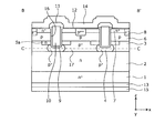
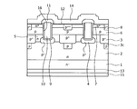
- FIG. 1A is a cross-sectional view showing a configuration of a silicon carbide semiconductor device according to Embodiment 1.
- FIG. 1B is a cross-sectional structure taken along the cutting line B-B ′ of FIG.
- FIG. 2 is a plan view showing an example of a planar layout of the silicon carbide semiconductor device according to the first embodiment.
- FIG. 3 is a cross-sectional view schematically showing a state in the process of manufacturing the silicon carbide semiconductor device according to the first embodiment (No. 1).
- FIG. 4 is a cross-sectional view schematically showing a state in the process of manufacturing the silicon carbide semiconductor device according to the first embodiment (No. 2).
- FIG. 1A is a cross-sectional view showing a configuration of a silicon carbide semiconductor device according to Embodiment 1.
- FIG. 1B is a cross-sectional structure taken along the cutting line B-B ′ of FIG.
- FIG. 2 is a plan view showing an example of a planar layout of the silicon carbide
- FIG. 5 is a cross-sectional view schematically showing a state in the process of manufacturing the silicon carbide semiconductor device according to the first embodiment (No. 3).
- FIG. 6 is a cross-sectional view schematically showing a state in the process of manufacturing the silicon carbide semiconductor device according to the first embodiment (No. 4).
- FIG. 7 is a cross-sectional view schematically showing a state in the process of manufacturing the silicon carbide semiconductor device according to the first embodiment (No. 5).
- FIG. 8 is a cross-sectional view schematically showing a state in the process of manufacturing the silicon carbide semiconductor device according to the first embodiment (No. 6).
- FIG. 9 is a cross sectional view showing an example of a state in which a lateral position between the trench and the second p + type base region is shifted in the example of the silicon carbide semiconductor device according to the first embodiment.
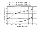
- FIG. 10 is a characteristic diagram showing a gate insulating film maximum electric field strength characteristic of an example of the silicon carbide semiconductor device according to the first embodiment.
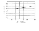
- FIG. 11 is a characteristic diagram showing on-resistance characteristics of an example of the silicon carbide semiconductor device according to the first embodiment.
- FIG. 12 is a cross-sectional view showing a configuration of the silicon carbide semiconductor device according to the second embodiment.
- FIG. 13 is a cross sectional view schematically showing a state in the process of manufacturing the silicon carbide semiconductor device according to the second embodiment.
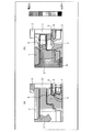
- FIG. 14 is a current distribution diagram at the time of avalanche breakdown in an example and a comparative example of the silicon carbide semiconductor device according to the second embodiment.
- the semiconductor device according to the present invention is configured using a wide band gap semiconductor.
- a silicon carbide semiconductor device manufactured using, for example, silicon carbide (SiC) as a wide band gap semiconductor will be described using MOSFET as an example.
- 1A is a cross-sectional view showing a configuration of a silicon carbide semiconductor device according to Embodiment 1.
- a silicon carbide semiconductor device includes a first main surface (front surface) of an n + -type silicon carbide substrate (first conductivity type wide bandgap semiconductor substrate) 1, for example, ( An n-type silicon carbide epitaxial layer (first conductivity type first wide band gap semiconductor layer) 2 is deposited on the (0001) plane (Si plane).
- n + type silicon carbide substrate 1 is a silicon carbide single crystal substrate doped with, for example, nitrogen (N).
- N-type silicon carbide epitaxial layer 2 is a low-concentration n-type drift layer doped with, for example, nitrogen at a lower impurity concentration than n + -type silicon carbide substrate 1.
- An n-type high concentration region (first conductivity type region) 5 is formed on the surface side of n-type silicon carbide epitaxial layer 2 opposite to the n + -type silicon carbide substrate 1 side.
- N type high concentration region 5 is a high concentration n type drift layer doped with, for example, nitrogen at an impurity concentration lower than that of n + type silicon carbide substrate 1 and higher than that of n type silicon carbide epitaxial layer 2.
- the n + -type silicon carbide substrate 1, the n-type silicon carbide epitaxial layer 2, and the p-type base layer (second conductivity type wide band gap semiconductor layer) 6 described later are combined to form a silicon carb
- a back surface electrode (drain electrode) 13 is provided on the second main surface (back surface, that is, the back surface of the silicon carbide semiconductor substrate) of n + type silicon carbide substrate 1.
- the back electrode 13 constitutes a drain electrode.
- a drain electrode pad 15 is provided on the surface of the back electrode 13.
- a trench structure is formed on the first main surface side (p-type base layer 6 side) of the silicon carbide semiconductor substrate. Specifically, trench 16 penetrates p-type base layer 6 from the surface opposite to the n + -type silicon carbide substrate 1 side of p-type base layer 6 (the first main surface side of the silicon carbide semiconductor substrate). As a result, the n-type high concentration region 5 is reached.
- a gate insulating film 9 is formed on the bottom and side walls of the trench 16 along the inner wall of the trench 16, and a gate electrode 10 is formed inside the gate insulating film 9 in the trench 16. Gate electrode 10 is insulated from n-type silicon carbide epitaxial layer 2 and p-type base layer 6 by gate insulating film 9. A part of the gate electrode 10 may protrude from the upper side of the trench 16 (source electrode pad 14 side) to the source electrode pad 14 side.
- the surface layer of the n-type silicon carbide epitaxial layer 2 opposite to the n + -type silicon carbide substrate 1 side has a first p + -type base region (second conductivity type).
- First base region) 3 and a second p + type base region (second conductivity type second base region) 4 are selectively provided.
- the first p + -type base region 3 reaches a position deeper on the drain side than the bottom of the trench 16.
- the lower end portion (drain side end portion) of the first p + -type base region 3 is located closer to the drain side than the bottom portion of the trench 16.
- the lower end portion of the second p + type base region 4 is located closer to the drain side than the bottom portion of the trench 16.
- the second p + -type base region 4 is formed at a position facing the bottom of the trench 16 in the depth direction z.
- the width of the second p + -type base region 4 is wider than the width of the trench 16.
- the bottom of the trench 16 may reach the second p + type base region 4, or may be located in the n type high concentration region 5 sandwiched between the p type base layer 6 and the second p + type base region 4, and It may not be in contact with the + type base region 4.
- the first p + type base region 3 and the second p + type base region 4 are doped with, for example, aluminum (Al).
- the 1p + -type base region 3 of a portion 17 is first 1p + -type base region 3 and the 2p + -type base region 4 and are aligned direction (hereinafter, referred to as a first direction) x
- a first direction A plane layout in which the n-type high concentration regions 5 are alternately and repeatedly arranged in a direction y (hereinafter referred to as a second direction) y may be provided.
- An example of a planar layout of the first and second p-type base regions 3 and 4 is shown in FIG. FIG.
- FIG. 2 is a plan view showing an example of a planar layout of the silicon carbide semiconductor device according to the first embodiment.
- FIG. 1A has a cross-sectional structure taken along section line AA ′ in FIG.
- FIG. 1B is a cross-sectional structure taken along the cutting line BB ′ in FIG.
- FIG. 2 is a plan layout along the section line CC in FIGS. 1A and 1B.
- the boundary between the first p + -type base region 3 and the second p + -type base region 4 is indicated by a vertical dotted line, and the first and second p-type base regions 3 and 4 are one part of the first p + -type base region 3.
- the state connected by the part 17 is shown (hatched part).
- the part 17 of the first p + -type base region 3 extends, for example, toward the trench 16 on both sides in the first direction x, and the second p + -type A part of the base region 4 is connected.
- a portion 5b on the drain side of the n-type high concentration region 5 is disposed between the portions 17 of the first p + -type base regions 3 adjacent to each other in the second direction y. That is, a portion 17 of the first p + -type base region 3 (a portion to which the first and second p-type base regions 3 and 4 are connected) sandwiches the drain-side portion 5b of the n-type high concentration region 5 in the second direction. periodically arranged at y.
- the n-type high concentration region 5 extends between a part 17 of the first p + -type base region 3 and the p-type base layer 6. That is, the portion 5a on the source side of the n-type high concentration region 5 is disposed between the p-type base layer 6 and the first and second p-type base regions 3 and 4 in the portion exposed at the sidewall of the trench 16. A part of the side surface of 16 is covered with an n-type region (FIG. 1B).
- FOG. 1B n-type region
- a p-type base layer (second conductivity type wide bandgap semiconductor layer) 6 is provided on the first main surface side of the base of the n-type silicon carbide epitaxial layer 2.
- the p-type base layer 6 is in contact with the first p + -type base region 3.
- the impurity concentration of the p-type base layer 6 may be lower than the impurity concentration of the first p + -type base region 3.
- an n + source region (first conductivity type source region) 7 and a p ++ contact region (second conductivity type contact region) 8 are selectively provided on the first main surface side of the substrate. Is provided. The n + source region 7 and the p ++ contact region 8 are in contact with each other. Further, a region sandwiched between the first p + -type base region 3 and the second p + -type base region 4 on the surface layer of the n-type silicon carbide epitaxial layer 2 on the first main surface side of the substrate, the p-type base layer 6 and the second p-type + n-type high-concentration region 5 is provided in an area sandwiched between the mold base region 4.
- FIG. 1A only two trench MOS structures are shown, but more trench structure MOS gate (insulated gates made of metal-oxide film-semiconductor) structures may be arranged in parallel.
- Interlayer insulating film 11 is provided on the entire first main surface side of the silicon carbide semiconductor substrate so as to cover gate electrode 10 embedded in the trench.
- Source electrode 12 is in contact with n + source region 7 and p ++ contact region 8 through a contact hole opened in interlayer insulating film 11.
- the source electrode 12 is electrically insulated from the gate electrode 10 by the interlayer insulating film 11.
- a source electrode pad 14 is provided on the source electrode 12.
- 3 to 8 are cross-sectional views schematically showing states during the manufacture of the silicon carbide semiconductor device according to the embodiment.
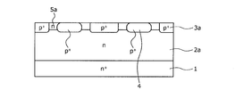
- an n + type silicon carbide substrate 1 made of n type silicon carbide is prepared.
- the wide band gap semiconductor layer 2a is epitaxially grown to a thickness of, for example, about 30 ⁇ m.
- This first n-type silicon carbide epitaxial layer 2 a becomes n-type silicon carbide epitaxial layer 2. The state up to here is shown in FIG.
- a mask (not shown) having a desired opening is formed on the surface of the first n-type silicon carbide epitaxial layer 2a by a photolithography technique, for example, using an oxide film. Then, using this oxide film as a mask, p-type impurities, for example, aluminum atoms are ion-implanted by ion implantation. Thereby, a first p-type region (second conductivity type first semiconductor region) 3a having a depth of, for example, about 0.5 ⁇ m and a second p + -type base region are formed in part of the surface region of the first n-type silicon carbide epitaxial layer 2a.
- (Second conductivity type second semiconductor region) 4 is formed, for example, such that the distance between adjacent first p-type region 3a and second p + -type base region 4 is about 1.5 ⁇ m.
- the dose amount during ion implantation for forming the first p-type region 3a and the second p + -type base region 4 may be set so that the impurity concentration is, for example, about 5 ⁇ 10 18 / cm 3 .
- n-type impurities such as nitrogen atoms are ion-implanted by ion implantation.
- a first n-type region having a depth of, for example, about 0.5 ⁇ m or less (the first n-type region) between the first p-type region 3a and the second p + -type base region 4 in the surface layer of the first n-type silicon carbide epitaxial layer 2a.
- Conductive type first region) 5a is formed.
- the dose amount at the time of ion implantation for forming the first n-type region 5a may be set so that, for example, the impurity concentration is about 1 ⁇ 10 17 / cm 3 . The state up to this point is shown in FIG.
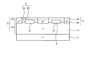
- a second n-type silicon carbide epitaxial layer (second first-conductivity-type wide bandgap semiconductor layer) 2b is doped on the surface of the first n-type silicon carbide epitaxial layer 2a while doping an n-type impurity such as a nitrogen atom. Is epitaxially grown to a thickness of, for example, about 0.5 ⁇ m.
- the second n-type silicon carbide epitaxial layer 2b and the first n-type silicon carbide epitaxial layer 2a are combined to form an n-type silicon carbide epitaxial layer 2.
- the epitaxial growth conditions for forming the second n-type silicon carbide epitaxial layer 2b may be set so that the impurity concentration of the second n-type silicon carbide epitaxial layer 2b is, for example, about 3 ⁇ 10 15 / cm 3 .
- a mask (not shown) having a desired opening is formed on the surface of the n-type silicon carbide epitaxial layer 2 by, for example, an oxide film by a photolithography technique. Then, using this oxide film as a mask, p-type impurities, for example, aluminum atoms are ion-implanted by ion implantation. As a result, a second p-type region (second conductive type third semiconductor region) 3b having a depth of, for example, about 0.5 ⁇ m is formed on a part of the surface region of the n-type silicon carbide epitaxial layer 2, for example, the first p-type region 3a. It is formed so as to overlap with the upper part.
- the second p-type region 3b and the first p-type region 3a are combined to form a first p + -type base region 3.
- the dose amount at the time of ion implantation for forming the second p-type region 3b may be set so that the impurity concentration is about 5 ⁇ 10 18 / cm 3 , for example.
- the mask used at the time of ion implantation for forming the second p-type region 3b is removed.
- n-type impurities such as nitrogen atoms are ion-implanted by ion implantation.
- a part of the surface layer of the second n-type silicon carbide epitaxial layer 2b is in contact with the first p-type region 3a, the second p + -type base region 4 and the first n-type region 5a, for example, with a depth of about 0.5 ⁇ m.
- the second n-type region (second region of the first conductivity type) 5b is formed.
- the dose amount at the time of ion implantation for providing the second n-type region 5b may be set so that, for example, the impurity concentration is about 1 ⁇ 10 17 / cm 3 .
- the second n-type region 5b and the first n-type region 5a are combined to form an n-type high concentration region 5. The state up to here is shown in FIG.
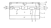
- a p-type base layer (doping with p-type impurities, for example, aluminum atoms)
- the wide band gap semiconductor layer (second conductivity type) 6 is epitaxially grown to a thickness of about 1.3 ⁇ m, for example.
- the epitaxial growth conditions for forming the p-type base layer 6 may be set such that the impurity concentration is about 4 ⁇ 10 17 / cm 3, which is lower than the impurity concentration of the first p + -type base region 3, for example.
- a mask (not shown) having a desired opening is formed on the surface of the p-type base layer 6 by, for example, an oxide film by photolithography.
- an n-type impurity such as phosphorus (P) is ion-implanted by ion implantation using this oxide film as a mask.
- an n + source region (first conductivity type source region) 7 is formed in a part of the surface layer of the p-type base layer 6.
- the dose at the time of ion implantation for forming the n + source region 7 may be set such that the impurity concentration is higher than that of the first p + type base region 3, for example.
- the mask used at the time of ion implantation for forming the n + source region 7 is removed.
- a mask (not shown) having a desired opening is formed by, for example, an oxide film on the surface of the p-type base layer 6 by photolithography, and the p-type is formed on the surface of the p-type base layer 6 using this oxide film as a mask.
- An impurity such as aluminum is ion-implanted.
- a p ++ contact region (second conductivity type contact region) 8 is formed in a part of the surface region of the p-type base layer 6.
- the dose amount at the time of ion implantation for forming the p ++ contact region 8 may be set such that the impurity concentration is higher than that of the second p + type base region 4, for example.
- the mask used at the time of ion implantation for forming the p ++ contact region 8 is removed.
- the order of ion implantation for forming n + source region 7 and ion implantation for forming p ++ contact region 8 may be interchanged. The state up to this point is shown in FIG.
- heat treatment is performed to activate, for example, the first p-type region 3a, the second p-type region 3b, the n + source region 7, and the p ++ contact region 8.
- the temperature of the heat treatment may be about 1700 ° C., for example.
- the heat treatment time may be, for example, about 2 minutes.
- the respective ion implantation regions may be activated collectively by one heat treatment, or may be activated by performing heat treatment every time ion implantation is performed.
- a mask (not shown) having a desired opening is formed by, for example, an oxide film by a photolithography technique.
- a trench 16 reaching the n-type high concentration region 5 through the n + source region 7 and the p-type base layer 6 is formed by dry etching or the like using this oxide film as a mask.
- the bottom of the trench 16 may reach the second p + type base region 4 or may be located in the n type high concentration region 5 sandwiched between the p type base layer 6 and the second p + type base region 4. Good.
- the mask used to form the trench 16 is removed. The state up to this point is shown in FIG.
- gate insulating film 9 is formed along the surfaces of n + source region 7 and p ++ contact region 8, and the bottom and side walls of trench 16.
- the gate insulating film 9 may be formed by thermal oxidation by heat treatment at a temperature of about 1000 ° C. in an oxygen atmosphere. Further, the gate insulating film 9 may be formed by a method of depositing by a chemical reaction such as high temperature oxidation (HTO).
- HTO high temperature oxidation
- a polycrystalline silicon layer doped with, for example, phosphorus atoms is formed on the gate insulating film 9.
- This polycrystalline silicon layer is formed so as to fill the trench 16.
- the gate electrode 10 is formed. A part of the gate electrode 10 may protrude from the upper side of the trench 16 (source electrode pad 14 side) to the source electrode pad 14 side.
- phosphor glass is formed to a thickness of about 1 ⁇ m so as to cover the gate insulating film 9 and the gate electrode 10 to form an interlayer insulating film 11.
- a contact hole is formed, and the n + source region 7 and the p ++ contact region 8 are exposed.
- heat treatment is performed to planarize the interlayer insulating film 11. The state up to this point is shown in FIG.
- a conductive film to be the source electrode 12 is formed in the contact hole and on the interlayer insulating film 11.
- the conductive film is selectively removed to leave the source electrode 12 only in the contact hole, for example.
- a drain electrode 13 made of, for example, a nickel (Ni) film is formed on the second main surface of the n + -type silicon carbide substrate 1. Thereafter, heat treatment is performed at a temperature of about 970 ° C., for example, to form ohmic contact between n + -type silicon carbide substrate 1 and drain electrode 13.
- an aluminum film is provided so as to cover the source electrode 12 and the interlayer insulating film 11 so as to cover the source electrode 12 and the interlayer insulating film 11, for example, by a sputtering method. Thereafter, the aluminum film is selectively removed and left so as to cover the active portion of the entire device, thereby forming the source electrode pad 14.
- the drain electrode pad 15 is formed on the surface of the drain electrode 13 by sequentially laminating, for example, titanium (Ti), nickel, and gold (Au). As described above, the semiconductor device shown in FIG. 1 is completed.
- FIG. 9 is a cross sectional view showing an example of a state in which a lateral position between the trench and the second p + type base region is shifted in the example of the silicon carbide semiconductor device according to the first embodiment.
- the horizontal direction is a direction in which the first and second p-type base regions 3 and 4 are arranged.
- the misalignment amount 101 is a lateral distance (unit: ⁇ m) between the center of the second p + -type base region 4 and the center of the trench 16, and the p-type base region width 102 is the second p + -type base.
- the trench width 103 is the width of the trench 16 (unit: ⁇ m).
- FIG. 10 is a characteristic diagram showing a maximum electric field strength characteristic of the gate insulating film of the example of the silicon carbide semiconductor device according to the first embodiment. 10, the misalignment of the 2p + -type base region 4 just below the trench 16, the variation of the gate insulating film 9 electric field strength when the center of the trench 16 is shifted laterally from the center of the 2p + -type base region 4 It is the result of having simulated.
- FIG. 10 also shows the relationship between the maximum electric field strength of the gate insulating film 9 and the misalignment of the comparative example.
- the p-type base region width 102 is 1 ⁇ m and the trench width 103 is 1 ⁇ m.
- the configuration other than the p-type base region width 102 of the comparative example is the same as that of the example.
- the p-type base region width 102 was 2 ⁇ m, and the trench width 103 was 1 ⁇ m.
- FIG. 10 is a result of simulating the maximum electric field strength applied to the gate insulating film 9 in the example and the comparative example. The amount of misalignment 101 when 4000 V is applied to the drain and the maximum electric field strength of the gate insulating film 9 are shown. It is a characteristic view which shows an example of a relationship. As shown in FIG.
- the example in which the p-type base region width 102 is wider than the trench width 103 is closer to the drain side than the comparative example in which the p-type base region width 102 is the same as the trench width 103. It was confirmed that the maximum electric field strength to the gate insulating film 9 when a voltage was applied was improved.
- FIG. 11 is a characteristic diagram showing on-resistance characteristics of an example of the silicon carbide semiconductor device according to the first embodiment.
- FIG. 11 also shows the on-resistance characteristics of the comparative example.
- FIG. 11 is a characteristic diagram showing an example of the on-resistance characteristics of the example and the comparative example of the semiconductor device according to the first embodiment, as a result of verifying the on-resistance characteristics of the example and the comparative example.
- the vertical axis represents on-resistance (unit: m ⁇ cm 2 )
- the horizontal axis represents p-type base region width 102 (unit: ⁇ m). As shown in FIG.
- the second n-type region 5b is formed by ion implantation.
- the second n-type silicon carbide epitaxial layer 2b may be formed as the second n-type region 5b. That is, a manufacturing method may be employed in which the impurity concentration of nitrogen is set to be the impurity concentration of the second n-type region 5b during the epitaxial growth of the second n-type silicon carbide epitaxial layer 2b, and ion implantation is omitted.
- n + type silicon carbide substrate 1 and the n type silicon carbide epitaxial layer 2 are combined to form a silicon carbide semiconductor substrate, and the p type base layer 6 is formed on the surface layer of the n type silicon carbide epitaxial layer 2 on the first main surface side of the substrate. It may be formed by ion implantation. Further, the n + -type silicon carbide substrate 1 alone is a silicon carbide semiconductor substrate, and all regions (n-type high-concentration regions 5) constituting the MOS gate structure on the surface layer on the first main surface side of the n + -type silicon carbide substrate 1 are used. And the first and second p-type base regions 3 and 4) may be formed by ion implantation.
- the first p + type base region in contact with the p type base layer, between the adjacent trenches, the position closer to the drain side than the bottom of the trench, A pn junction between the first p + type base region and the n type drift layer can be formed. Further, by providing a second p + -type base region inside the n-type drift layer so as to surround the trench bottom or to be deeper than the trench bottom and opposed to the trench in the depth direction, the bottom of the trench is formed. A pn junction between the second p + type base region and the n type drift layer can be formed at a close position.
- a portion of the 1p + -type base region extends to the trench side and it is connected to the 2p + -type base region, the 2p + -type base region and the n-type Holes generated when avalanche breakdown occurs at the junction of the silicon carbide epitaxial layer can be efficiently retracted to the source electrode. For this reason, the on-resistance can be lowered while the withstand voltage is high.
- a second p + -type base region is arranged so as to surround at least one corner of the trench bottom.
- FIG. 12 is a cross-sectional view showing a configuration of the silicon carbide semiconductor device according to the second embodiment of the present invention.
- the silicon carbide semiconductor device according to the second embodiment is in contact with the lower end portion (drain side end portion) of first p + -type base region 3 inside n-type silicon carbide epitaxial layer 2.
- the third p-type region 3c is provided.
- the third p-type region 3 c functions as a base region together with the p-type base layer 6 and the first p + -type base region 3.
- the thickness of the third p-type region 3c may be, for example, about 0.1 ⁇ m to 0.5 ⁇ m.
- the width of the third p-type region 3c is narrower than the width of the first p + -type base region 3, for example, the first p + type It may be narrower by 0.1 ⁇ m or more than the mold base region 3.
- the third p-type region 3c may be provided with the same thickness continuously along the side wall direction of the first p + -type base region 3 and the direction parallel to the surface of the n + silicon carbide substrate 1. When viewed from the + side of the silicon carbide substrate 1, it may be provided in a periodic dot shape.
- FIG. 13 is a cross sectional view schematically showing a state in the process of manufacturing the silicon carbide semiconductor device according to the second embodiment.
- the mask used at the time of ion implantation is removed.
- a mask (not shown) having a desired opening is formed on the surface of the first n-type silicon carbide epitaxial layer 2a by a photolithography technique, for example, with a resist.
- the third p-type region 3c having a thickness of about 0.25 ⁇ m, for example, is in contact with the first p-type region 3a at the lower part (drain side end) of the first p-type region 3a.
- the ion energy for forming the third p-type region 3c may be set to, for example, 700 keV, and the dose amount to, for example, about 1 ⁇ 10 14 / cm 2 .
- FIG. 14 is a current distribution diagram at the time of avalanche breakdown in an example and a comparative example of the silicon carbide semiconductor device according to the second embodiment.
- the avalanche breakdown occurred in the structure in which the third p-type region 3c was formed as an example (FIG. 14B) and in the structure in which the third p-type region 3c was not formed as a comparative example (FIG. 14A).
- the change in the in-plane distribution (cross-sectional view) of the current value was evaluated.
- FIG. 14A in the comparative example, it can be seen that avalanche breakdown occurs in the second p + type base region 4 immediately below the gate electrode 10, and a large amount of current flows directly below the gate electrode 10.
- the avalanche breakdown occurs in the third p-type region 3c, and the current path flows from the n + source region 7 through the third p-type region 3c to the drain side.
- I can confirm.
- a similar result occurs when the thickness of the third p-type region 3c is 0.1 ⁇ m or more and the width is 0.1 ⁇ m or more narrower than that of the first p + -type base region 3.
- the second embodiment As described above, according to the second embodiment, as in the first embodiment, even when a wide band gap semiconductor is used as a semiconductor material, there is an effect that a high withstand voltage can be achieved. Further, according to the second embodiment, by deeper than at least a portion of the lower end portion of the 1p + type base region (second 3p-type region) lower end portion of the 2p + -type base region, occurred avalanche breakdown Current flows from the source region through the third p-type region to the drain side. For this reason, the electric field strength of the gate insulating film at the bottom of the trench can be further relaxed.
- the case where the first main surface of the silicon carbide substrate made of silicon carbide is the (0001) plane and the MOS gate structure is formed on the (0001) plane has been described as an example.
- Various types of wide band gap semiconductors for example, gallium nitride (GaN)), surface orientation of the substrate main surface, and the like can be variously changed.
- the first conductivity type is n-type and the second conductivity type is p-type.
- the first conductivity type is p-type and the second conductivity type is n-type. The same holds true.
- the semiconductor device according to the present invention is useful for a high voltage semiconductor device used for a power conversion device, a power supply device such as various industrial machines, and the like.
Landscapes
- Electrodes Of Semiconductors (AREA)
Abstract
Description
本発明にかかる半導体装置は、ワイドバンドギャップ半導体を用いて構成される。実施の形態においては、ワイドバンドギャップ半導体として例えば炭化珪素(SiC)を用いて作製された炭化珪素半導体装置について、MOSFETを例に説明する。図1Aは、実施の形態1にかかる炭化珪素半導体装置の構成を示す断面図である。
次に、実施の形態にかかる炭化珪素半導体装置の製造方法について説明する。図3~図8は、実施の形態にかかる炭化珪素半導体装置の製造途中の状態を模式的に示す断面図である。
図9は、実施の形態1にかかる炭化珪素半導体装置の実施例においてトレンチと第2p+型ベース領域との横方向位置にズレが生じた状態の一例を示す断面図である。横方向とは、第1,2p型ベース領域3,4が並ぶ方向である。ここで、合わせズレ量101は、第2p+型ベース領域4の中心とトレンチ16の中心との横方向の距離(単位:μm)であり、p型ベース領域幅102は、第2p+型ベース領域4の幅(単位:μm)であり、トレンチ幅103は、トレンチ16の幅(単位:μm)である。
図12は、本発明の実施の形態2にかかる炭化珪素半導体装置の構成を示す断面図である。図12に示すように、実施の形態2にかかる炭化珪素半導体装置は、n型炭化珪素エピタキシャル層2の内部に、第1p+型ベース領域3の下端部(ドレイン側端部)に接するように第3p型領域3cを設けた構造である。第3p型領域3cは、p型ベース層6および第1p+型ベース領域3とともにベース領域として機能する。
図13は、実施の形態2にかかる炭化珪素半導体装置の製造途中の状態を模式的に示す断面図である。図13に示すように、第1p型領域3a、第2p+型ベース領域4、第1n型領域5aを形成した後、イオン注入時に用いたマスクを除去する。その後、第1n型炭化珪素エピタキシャル層2aの表面上に、フォトリソグラフィ技術によって所望の開口部を有する図示しないマスクを、例えばレジストで形成する。そして、このレジストをマスクとしてイオン注入法によってp型の不純物、例えばアルミニウム原子をイオン注入する。それによって、図13に示すように、第1p型領域3aの下部(ドレイン側端部)に、第1p型領域3aに接するように、例えば厚さ0.25μm程度の第3p型領域3cが、例えば幅1μm程度となるように、形成される。第3p型領域3cを形成する際のイオンのエネルギーを、例えば700keV、ドーズ量を、例えば1×10¹⁴/cm2程度となるように設定してもよい。
図14は、実施の形態2にかかる炭化珪素半導体装置の実施例と比較例におけるアバランシェ降伏時の電流分布図である。図14では、実施例として第3p型領域3cを形成した構造(図14(b))と、比較例として第3p型領域3cを形成しない構造(図14(a))によるアバランシェ降伏が起こったときの電流値の面内分布(断面図)の変化を評価した。図14(a)に示すように、比較例ではゲート電極10直下の第2p+型ベース領域4でアバランシェ降伏が起こり、ゲート電極10直下で電流が多く流れることが分かる。一方、図14(b)に示すように、実施例ではアバランシェ降伏が第3p型領域3cで発生し、電流経路がn+ソース領域7から第3p型領域3cを通過しドレイン側へ流れることが確認できる。同様の結果は、第3p型領域3cの厚さが0.1μm以上、幅が第1p+型ベース領域3よりも0.1μm以上狭ければ起こる。
2 n型炭化珪素エピタキシャル層
2a 第1n型炭化珪素エピタキシャル層
2b 第2n型炭化珪素エピタキシャル層
3 第1p+型ベース領域
3a 第1p型領域
3b 第2p型領域
3c 第3p型領域
4 第2p+型ベース領域
5 n型高濃度領域
5a 第1n型領域
5b 第2n型領域
6 p型ベース層
7 n+ソース領域
8 p++コンタクト領域
9 ゲート絶縁膜
10 ゲート電極
11 層間絶縁膜
12 ソース電極
13 ソース裏面電極
14 ソース電極パッド
15 ドレイン電極パッド
16 トレンチ
Claims (13)
- シリコンよりもバンドギャップが広い半導体からなる第1導電型のワイドバンドギャップ半導体基板と、
前記ワイドバンドギャップ半導体基板のおもて面に形成された、シリコンよりもバンドギャップが広い半導体からなる、前記ワイドバンドギャップ半導体基板より低不純物濃度の第1導電型ワイドバンドギャップ半導体層と、
前記第1導電型ワイドバンドギャップ半導体層の前記ワイドバンドギャップ半導体基板側に対して反対側の表面層に選択的に形成された第2導電型の第1ベース領域と、
前記第1導電型ワイドバンドギャップ半導体層の内部に選択的に形成された第2導電型の第2ベース領域と、
前記第1導電型ワイドバンドギャップ半導体層の前記ワイドバンドギャップ半導体基板側に対して反対側の表面層に選択的に形成された、前記第1導電型ワイドバンドギャップ半導体層より高不純物濃度の第1導電型の領域と、
前記第1導電型ワイドバンドギャップ半導体層の前記ワイドバンドギャップ半導体基板に対して反対側の表面に形成された、シリコンよりもバンドギャップが広い半導体からなる第2導電型ワイドバンドギャップ半導体層と、
前記第2導電型ワイドバンドギャップ半導体層の内部に選択的に形成された第1導電型のソース領域と、
前記第2導電型ワイドバンドギャップ半導体層および前記ソース領域を貫通して前記第1導電型の領域に達するトレンチと、
前記トレンチ内部にゲート絶縁膜を介して形成されたゲート電極と、
前記第2導電型ワイドバンドギャップ半導体層および前記ソース領域に接触するソース電極と、
前記ワイドバンドギャップ半導体基板の裏面に設けられたドレイン電極と、
を備え、
前記第2ベース領域は、前記トレンチと深さ方向に対向する位置に配置され、
前記第1ベース領域の一部は、前記トレンチ側に延在し、前記第2ベース領域に接続されていることを特徴とする半導体装置。 - 前記第2ベース領域の幅は、前記トレンチの幅よりも広いことを特徴とする請求項1に記載の半導体装置。
- 前記トレンチは、前記第1導電型の領域を貫通して前記第2ベース領域に達することを特徴とする請求項1に記載の半導体装置。
- 前記第1ベース領域の一部と前記第2ベース領域との接続部分と、前記第2導電型ワイドバンドギャップ半導体層との間に、前記第1導電型の領域が延在していることを特徴とする請求項1に記載の半導体装置。
- 前記第1導電型の領域を挟んで、前記第1ベース領域の一部と前記第2ベース領域との接続部分を、前記第1ベース領域と前記第2ベース領域とが並ぶ方向と直交する方向に周期的に配置した平面レイアウトを有することを特徴とする請求項1に記載の半導体装置。
- 前記第1ベース領域の前記ドレイン電極側の端部の少なくとも一部は、前記第2ベース領域の前記ドレイン電極側の端部のよりも前記ドレイン電極側に位置することを特徴とする請求項1に記載の半導体装置。
- 前記第1ベース領域の前記ドレイン電極側の端部の、前記第2ベース領域の前記ドレイン電極側の端部よりも深い部分を、前記第1ベース領域と前記第2ベース領域とが並ぶ方向と直交する方向に周期的に配置した平面レイアウトを有することを特徴とする請求項1に記載の半導体装置。
- シリコンよりもバンドギャップが広い半導体は、炭化珪素であることを特徴とする請求項1~7のいずれか一つに記載の半導体装置。
- シリコンよりもバンドギャップが広い半導体からなる第1導電型のワイドバンドギャップ半導体基板のおもて面に、前記ワイドバンドギャップ半導体基板より低不純物濃度の第1の第1導電型ワイドバンドギャップ半導体層を形成する第1工程と、
前記第1の第1導電型ワイドバンドギャップ半導体層の表面層に、第2導電型の第1半導体領域および第2導電型の第2半導体領域を選択的に形成する第2工程と、
前記第1の第1導電型ワイドバンドギャップ半導体層の表面に、シリコンよりもバンドギャップが広い半導体からなる、前記ワイドバンドギャップ半導体基板より低不純物濃度の第2の第1導電型ワイドバンドギャップ半導体層を形成する第3工程と、
前記第2の第1導電型ワイドバンドギャップ半導体層の表面層に、前記第1半導体領域に接する第2導電型の第3半導体領域を選択的に形成する第4工程と、
前記第2の第1導電型ワイドバンドギャップ半導体層の表面に、シリコンよりもバンドギャップが広い半導体からなる第2導電型ワイドバンドギャップ半導体層を形成する第5工程と、
前記第2導電型ワイドバンドギャップ半導体層の内部に第1導電型のソース領域を選択的に形成する第6工程と、
前記ソース領域および前記第2導電型ワイドバンドギャップ半導体層を貫通して前記第1導電型の第1領域に達するトレンチを、前記第2半導体領域と深さ方向に対向する位置に形成する第7工程と、
前記トレンチの内部にゲート絶縁膜を介してゲート電極を形成する第8工程と、
前記第2導電型ワイドバンドギャップ半導体層および前記ソース領域に接するソース電極を形成する第9工程と、
前記ワイドバンドギャップ半導体基板の裏面にドレイン電極を形成する第10工程と、
を含み、
前記第2工程では、前記第1半導体領域と前記第2半導体領域との間に前記第1の第1導電型ワイドバンドギャップ半導体層が残るように、前記第1半導体領域の一部と前記第2半導体領域とを接続させることを特徴とする半導体装置の製造方法。 - 前記第4工程では、前記第1ベース領域の、前記第2ベース領域との接続部分以外の部分に接する前記第3半導体領域を形成することを特徴とする請求項9に記載の半導体装置の製造方法。
- 前記第1工程の後、前記第3工程の前に、前記第1の第1導電型ワイドバンドギャップ半導体層の表面層の、前記第1半導体領域および前記第2半導体領域との間に第1導電型の第1領域を形成する工程をさらに含むことを特徴とする請求項9に記載の半導体装置の製造方法。
- 前記第3工程の後、前記第5工程の前に、前記第2の第1導電型ワイドバンドギャップ半導体層の表面層に、前記第1領域に接する第1導電型の第2領域を選択的に形成する工程をさらに含むことを特徴とする請求項11に記載の半導体装置の製造方法。
- 前記第1工程の後、前記第3工程の前に、前記第1半導体領域よりも深い位置に、前記第1半導体領域に接する第2導電型の第4半導体領域を形成する工程をさらに含むことを特徴とする請求項9~12のいずれか一つに記載の半導体装置の製造方法。
Priority Applications (5)
| Application Number | Priority Date | Filing Date | Title |
|---|---|---|---|
| JP2017545120A JP6778373B2 (ja) | 2015-10-16 | 2016-09-08 | 半導体装置および半導体装置の製造方法 |
| CN201680050777.6A CN108352402B (zh) | 2015-10-16 | 2016-09-08 | 半导体装置和半导体装置的制造方法 |
| DE112016003510.1T DE112016003510B4 (de) | 2015-10-16 | 2016-09-08 | HALBLEITERVORRlCHTUNG UND VERFAHREN ZUR HERSTELLUNG EINER HALBLEITERVORRICHTUNG |
| US15/909,971 US10199493B2 (en) | 2015-10-16 | 2018-03-01 | Semiconductor device and method of manufacturing semiconductor device |
| US16/263,643 US10403749B2 (en) | 2015-10-16 | 2019-01-31 | Method of manufacturing semiconductor device |
Applications Claiming Priority (2)
| Application Number | Priority Date | Filing Date | Title |
|---|---|---|---|
| JP2015204672 | 2015-10-16 | ||
| JP2015-204672 | 2015-10-16 |
Related Child Applications (1)
| Application Number | Title | Priority Date | Filing Date |
|---|---|---|---|
| US15/909,971 Continuation US10199493B2 (en) | 2015-10-16 | 2018-03-01 | Semiconductor device and method of manufacturing semiconductor device |
Publications (1)
| Publication Number | Publication Date |
|---|---|
| WO2017064949A1 true WO2017064949A1 (ja) | 2017-04-20 |
Family
ID=58518233
Family Applications (1)
| Application Number | Title | Priority Date | Filing Date |
|---|---|---|---|
| PCT/JP2016/076419 Ceased WO2017064949A1 (ja) | 2015-10-16 | 2016-09-08 | 半導体装置および半導体装置の製造方法 |
Country Status (5)
| Country | Link |
|---|---|
| US (2) | US10199493B2 (ja) |
| JP (2) | JP6778373B2 (ja) |
| CN (1) | CN108352402B (ja) |
| DE (1) | DE112016003510B4 (ja) |
| WO (1) | WO2017064949A1 (ja) |
Cited By (22)
| Publication number | Priority date | Publication date | Assignee | Title |
|---|---|---|---|---|
| CN107658260A (zh) * | 2017-08-08 | 2018-02-02 | 全球能源互联网研究院有限公司 | 在基板上形成绝缘沟槽的方法及半导体器件 |
| JP2018201013A (ja) * | 2017-05-26 | 2018-12-20 | 富士電機株式会社 | 炭化ケイ素半導体装置 |
| JP2018206923A (ja) * | 2017-06-02 | 2018-12-27 | 富士電機株式会社 | 絶縁ゲート型半導体装置及びその製造方法 |
| JP2019071312A (ja) * | 2017-10-05 | 2019-05-09 | 富士電機株式会社 | 半導体装置 |
| JP2019087647A (ja) * | 2017-11-07 | 2019-06-06 | 富士電機株式会社 | 絶縁ゲート型半導体装置及びその製造方法 |
| JP2019102555A (ja) * | 2017-11-29 | 2019-06-24 | 国立研究開発法人産業技術総合研究所 | 半導体装置 |
| JP2019114724A (ja) * | 2017-12-25 | 2019-07-11 | 富士電機株式会社 | 半導体装置および半導体装置の製造方法 |
| JP2019208074A (ja) * | 2015-10-16 | 2019-12-05 | 富士電機株式会社 | 半導体装置 |
| JP2020107646A (ja) * | 2018-12-26 | 2020-07-09 | 住重アテックス株式会社 | 半導体装置および半導体装置の製造方法 |
| JP2020191421A (ja) * | 2019-05-23 | 2020-11-26 | 富士電機株式会社 | 半導体装置 |
| US11205719B2 (en) | 2019-03-22 | 2021-12-21 | Fuji Electric Co., Ltd. | Insulated-gate semiconductor device |
| JP2021197384A (ja) * | 2020-06-09 | 2021-12-27 | 富士電機株式会社 | 半導体装置 |
| US11569376B2 (en) | 2019-09-06 | 2023-01-31 | Fuji Electric Co., Ltd. | Silicon carbide semiconductor device and method of manufacturing silicon carbide semiconductor device |
| JP2023031337A (ja) * | 2021-08-25 | 2023-03-09 | 富士電機株式会社 | 炭化珪素半導体装置、炭化珪素半導体装置の製造方法および半導体回路装置 |
| CN117558761A (zh) * | 2024-01-10 | 2024-02-13 | 湖北九峰山实验室 | 一种宽禁带半导体沟槽mosfet器件及其制造方法 |
| US12040361B2 (en) | 2021-01-22 | 2024-07-16 | Fuji Electric Co., Ltd. | Semiconductor device |
| US12068366B2 (en) | 2021-03-30 | 2024-08-20 | Fuji Electric Co., Ltd. | Semiconductor device |
| US12170312B2 (en) | 2021-03-08 | 2024-12-17 | Fuji Electric Co., Ltd. | Super junction silicon carbide semiconductor device and manufacturing method thereof |
| US12205990B2 (en) | 2021-06-07 | 2025-01-21 | Fuji Electric Co., Ltd. | Method of manufacturing silicon carbide semiconductor device and silicon carbide semiconductor device |
| US12408390B2 (en) | 2021-06-15 | 2025-09-02 | Fuji Electric Co., Ltd. | Semiconductor device |
| US12464783B2 (en) | 2021-03-08 | 2025-11-04 | Fuji Electric Co., Ltd. | Insulated gate semiconductor device |
| US12563792B2 (en) | 2020-12-24 | 2026-02-24 | Fuji Electric Co., Ltd. | Insulated gate semiconductor device |
Families Citing this family (18)
| Publication number | Priority date | Publication date | Assignee | Title |
|---|---|---|---|---|
| JP6115678B1 (ja) * | 2016-02-01 | 2017-04-19 | 富士電機株式会社 | 炭化珪素半導体装置および炭化珪素半導体装置の製造方法 |
| JP6658257B2 (ja) * | 2016-04-22 | 2020-03-04 | 住友電気工業株式会社 | 炭化珪素半導体装置 |
| JP6896672B2 (ja) * | 2018-03-21 | 2021-06-30 | 株式会社東芝 | 半導体装置及びその製造方法 |
| DE102018123210B3 (de) * | 2018-09-20 | 2020-02-27 | Infineon Technologies Ag | Siliziumkarbid-Bauelemente und Verfahren zum Bilden von Siliziumkarbid-Bauelementen |
| US11069770B2 (en) * | 2018-10-01 | 2021-07-20 | Ipower Semiconductor | Carrier injection control fast recovery diode structures |
| WO2020110514A1 (ja) * | 2018-11-29 | 2020-06-04 | 富士電機株式会社 | 超接合炭化珪素半導体装置および超接合炭化珪素半導体装置の製造方法 |
| JP7275573B2 (ja) * | 2018-12-27 | 2023-05-18 | 富士電機株式会社 | 炭化珪素半導体装置および炭化珪素半導体装置の製造方法 |
| DE102019212649A1 (de) * | 2019-08-23 | 2021-02-25 | Robert Bosch Gmbh | Halbleitervorrichtung und Verfahren zum Herstellen einer Halbleitervorrichtung |
| JP7327283B2 (ja) * | 2020-05-29 | 2023-08-16 | 豊田合成株式会社 | 半導体装置 |
| JP7721928B2 (ja) * | 2021-03-08 | 2025-08-13 | 富士電機株式会社 | 窒化物半導体装置 |
| JP7187620B1 (ja) * | 2021-07-13 | 2022-12-12 | 昭和電工株式会社 | SiCエピタキシャルウェハ及びSiCエピタキシャルウェハの製造方法 |
| CN113345965B (zh) * | 2021-08-05 | 2021-11-09 | 浙江大学杭州国际科创中心 | 一种具有电场屏蔽结构的沟槽栅mosfet器件 |
| CN113838910A (zh) * | 2021-08-24 | 2021-12-24 | 深圳深爱半导体股份有限公司 | 功率器件及制备方法 |
| JP7577635B2 (ja) * | 2021-09-22 | 2024-11-05 | 東芝デバイス&ストレージ株式会社 | 半導体装置及び半導体装置の製造方法 |
| JP7702911B2 (ja) * | 2022-03-18 | 2025-07-04 | 株式会社東芝 | 半導体装置およびその製造方法 |
| CN116504808B (zh) * | 2023-04-18 | 2025-09-26 | 湖北九峰山实验室 | 宽禁带半导体包角沟槽mosfet器件结构及其制作方法 |
| CN116598347B (zh) * | 2023-07-19 | 2023-09-29 | 北京昕感科技有限责任公司 | 具有曲面栅极沟槽的SiC MOSFET元胞结构、器件及制备方法 |
| CN118553793B (zh) * | 2024-07-25 | 2024-10-25 | 恒泰柯半导体(上海)有限公司 | 一种碳化硅功率器件及其制备方法 |
Citations (2)
| Publication number | Priority date | Publication date | Assignee | Title |
|---|---|---|---|---|
| JP2012169385A (ja) * | 2011-02-11 | 2012-09-06 | Denso Corp | 炭化珪素半導体装置 |
| JP2012169384A (ja) * | 2011-02-11 | 2012-09-06 | Denso Corp | 炭化珪素半導体装置およびその製造方法 |
Family Cites Families (19)
| Publication number | Priority date | Publication date | Assignee | Title |
|---|---|---|---|---|
| JPS5539931A (en) | 1978-09-13 | 1980-03-21 | Nissan Motor Co Ltd | Process control device |
| US6180958B1 (en) | 1997-02-07 | 2001-01-30 | James Albert Cooper, Jr. | Structure for increasing the maximum voltage of silicon carbide power transistors |
| JP4061711B2 (ja) * | 1998-06-18 | 2008-03-19 | 株式会社デンソー | Mosトランジスタ及びその製造方法 |
| JP4738562B2 (ja) * | 2000-03-15 | 2011-08-03 | 三菱電機株式会社 | 半導体装置の製造方法 |
| JP5721308B2 (ja) | 2008-03-26 | 2015-05-20 | ローム株式会社 | 半導体装置 |
| JP5531787B2 (ja) * | 2010-05-31 | 2014-06-25 | 株式会社デンソー | 炭化珪素半導体装置およびその製造方法 |
| US8525254B2 (en) | 2010-08-12 | 2013-09-03 | Infineon Technologies Austria Ag | Silicone carbide trench semiconductor device |
| WO2012165329A1 (ja) * | 2011-05-27 | 2012-12-06 | 新電元工業株式会社 | トレンチゲートパワー半導体装置及びその製造方法 |
| JP5745997B2 (ja) * | 2011-10-31 | 2015-07-08 | トヨタ自動車株式会社 | スイッチング素子とその製造方法 |
| US9337271B2 (en) * | 2012-12-28 | 2016-05-10 | Mitsubishi Electric Corporation | Silicon-carbide semiconductor device and manufacturing method therefor |
| US9142668B2 (en) | 2013-03-13 | 2015-09-22 | Cree, Inc. | Field effect transistor devices with buried well protection regions |
| JP2015072999A (ja) * | 2013-10-02 | 2015-04-16 | 株式会社デンソー | 炭化珪素半導体装置 |
| JP6341074B2 (ja) * | 2014-01-24 | 2018-06-13 | 株式会社デンソー | 半導体装置の製造方法 |
| JP6627757B2 (ja) | 2014-06-30 | 2020-01-08 | 住友電気工業株式会社 | 炭化珪素半導体装置およびその製造方法 |
| WO2016002766A1 (ja) * | 2014-06-30 | 2016-01-07 | 国立研究開発法人産業技術総合研究所 | 炭化珪素半導体装置およびその製造方法 |
| WO2017043607A1 (ja) | 2015-09-09 | 2017-03-16 | 住友電気工業株式会社 | 縦型炭化珪素半導体装置のトレンチのアニール処理装置、縦型炭化珪素半導体装置の製造方法および縦型炭化珪素半導体装置 |
| CN108352402B (zh) * | 2015-10-16 | 2020-12-18 | 富士电机株式会社 | 半导体装置和半导体装置的制造方法 |
| JP6801323B2 (ja) * | 2016-09-14 | 2020-12-16 | 富士電機株式会社 | 半導体装置および半導体装置の製造方法 |
| JP2019004010A (ja) * | 2017-06-14 | 2019-01-10 | 富士電機株式会社 | 半導体装置およびその製造方法 |
-
2016
- 2016-09-08 CN CN201680050777.6A patent/CN108352402B/zh active Active
- 2016-09-08 JP JP2017545120A patent/JP6778373B2/ja active Active
- 2016-09-08 DE DE112016003510.1T patent/DE112016003510B4/de active Active
- 2016-09-08 WO PCT/JP2016/076419 patent/WO2017064949A1/ja not_active Ceased
-
2018
- 2018-03-01 US US15/909,971 patent/US10199493B2/en active Active
-
2019
- 2019-01-31 US US16/263,643 patent/US10403749B2/en active Active
- 2019-08-09 JP JP2019148138A patent/JP6874797B2/ja active Active
Patent Citations (2)
| Publication number | Priority date | Publication date | Assignee | Title |
|---|---|---|---|---|
| JP2012169385A (ja) * | 2011-02-11 | 2012-09-06 | Denso Corp | 炭化珪素半導体装置 |
| JP2012169384A (ja) * | 2011-02-11 | 2012-09-06 | Denso Corp | 炭化珪素半導体装置およびその製造方法 |
Cited By (36)
| Publication number | Priority date | Publication date | Assignee | Title |
|---|---|---|---|---|
| JP2019208074A (ja) * | 2015-10-16 | 2019-12-05 | 富士電機株式会社 | 半導体装置 |
| JP2018201013A (ja) * | 2017-05-26 | 2018-12-20 | 富士電機株式会社 | 炭化ケイ素半導体装置 |
| JP7139678B2 (ja) | 2017-05-26 | 2022-09-21 | 富士電機株式会社 | 炭化ケイ素半導体装置 |
| JP2018206923A (ja) * | 2017-06-02 | 2018-12-27 | 富士電機株式会社 | 絶縁ゲート型半導体装置及びその製造方法 |
| JP7081087B2 (ja) | 2017-06-02 | 2022-06-07 | 富士電機株式会社 | 絶縁ゲート型半導体装置及びその製造方法 |
| CN107658260A (zh) * | 2017-08-08 | 2018-02-02 | 全球能源互联网研究院有限公司 | 在基板上形成绝缘沟槽的方法及半导体器件 |
| JP2019071312A (ja) * | 2017-10-05 | 2019-05-09 | 富士電機株式会社 | 半導体装置 |
| JP6992388B2 (ja) | 2017-10-05 | 2022-01-13 | 富士電機株式会社 | 半導体装置 |
| JP2019087647A (ja) * | 2017-11-07 | 2019-06-06 | 富士電機株式会社 | 絶縁ゲート型半導体装置及びその製造方法 |
| US11329151B2 (en) | 2017-11-07 | 2022-05-10 | Fuji Electric Co., Ltd. | Insulated-gate semiconductor device and method of manufacturing the same |
| JP7067021B2 (ja) | 2017-11-07 | 2022-05-16 | 富士電機株式会社 | 絶縁ゲート型半導体装置及びその製造方法 |
| JP2019102555A (ja) * | 2017-11-29 | 2019-06-24 | 国立研究開発法人産業技術総合研究所 | 半導体装置 |
| JP7057555B2 (ja) | 2017-11-29 | 2022-04-20 | 国立研究開発法人産業技術総合研究所 | 半導体装置 |
| US11437508B2 (en) | 2017-11-29 | 2022-09-06 | Fuji Electric Co., Ltd. | Semiconductor device |
| JP2019114724A (ja) * | 2017-12-25 | 2019-07-11 | 富士電機株式会社 | 半導体装置および半導体装置の製造方法 |
| JP7062946B2 (ja) | 2017-12-25 | 2022-05-09 | 富士電機株式会社 | 半導体装置および半導体装置の製造方法 |
| JP2020107646A (ja) * | 2018-12-26 | 2020-07-09 | 住重アテックス株式会社 | 半導体装置および半導体装置の製造方法 |
| JP7169872B2 (ja) | 2018-12-26 | 2022-11-11 | 住重アテックス株式会社 | 半導体装置および半導体装置の製造方法 |
| US11205719B2 (en) | 2019-03-22 | 2021-12-21 | Fuji Electric Co., Ltd. | Insulated-gate semiconductor device |
| JP2020191421A (ja) * | 2019-05-23 | 2020-11-26 | 富士電機株式会社 | 半導体装置 |
| JP7302286B2 (ja) | 2019-05-23 | 2023-07-04 | 富士電機株式会社 | 半導体装置 |
| US11133300B2 (en) | 2019-05-23 | 2021-09-28 | Fuji Electric Co., Ltd. | Semiconductor device |
| US11569376B2 (en) | 2019-09-06 | 2023-01-31 | Fuji Electric Co., Ltd. | Silicon carbide semiconductor device and method of manufacturing silicon carbide semiconductor device |
| JP7532921B2 (ja) | 2020-06-09 | 2024-08-14 | 富士電機株式会社 | 半導体装置 |
| JP2021197384A (ja) * | 2020-06-09 | 2021-12-27 | 富士電機株式会社 | 半導体装置 |
| US12563792B2 (en) | 2020-12-24 | 2026-02-24 | Fuji Electric Co., Ltd. | Insulated gate semiconductor device |
| US12040361B2 (en) | 2021-01-22 | 2024-07-16 | Fuji Electric Co., Ltd. | Semiconductor device |
| US12170312B2 (en) | 2021-03-08 | 2024-12-17 | Fuji Electric Co., Ltd. | Super junction silicon carbide semiconductor device and manufacturing method thereof |
| US12464783B2 (en) | 2021-03-08 | 2025-11-04 | Fuji Electric Co., Ltd. | Insulated gate semiconductor device |
| US12068366B2 (en) | 2021-03-30 | 2024-08-20 | Fuji Electric Co., Ltd. | Semiconductor device |
| US12205990B2 (en) | 2021-06-07 | 2025-01-21 | Fuji Electric Co., Ltd. | Method of manufacturing silicon carbide semiconductor device and silicon carbide semiconductor device |
| US12408390B2 (en) | 2021-06-15 | 2025-09-02 | Fuji Electric Co., Ltd. | Semiconductor device |
| JP2023031337A (ja) * | 2021-08-25 | 2023-03-09 | 富士電機株式会社 | 炭化珪素半導体装置、炭化珪素半導体装置の製造方法および半導体回路装置 |
| JP7711489B2 (ja) | 2021-08-25 | 2025-07-23 | 富士電機株式会社 | 炭化珪素半導体装置、炭化珪素半導体装置の製造方法および半導体回路装置 |
| CN117558761A (zh) * | 2024-01-10 | 2024-02-13 | 湖北九峰山实验室 | 一种宽禁带半导体沟槽mosfet器件及其制造方法 |
| CN117558761B (zh) * | 2024-01-10 | 2024-04-05 | 湖北九峰山实验室 | 一种宽禁带半导体沟槽mosfet器件及其制造方法 |
Also Published As
| Publication number | Publication date |
|---|---|
| US20180197983A1 (en) | 2018-07-12 |
| CN108352402A (zh) | 2018-07-31 |
| JP2019208074A (ja) | 2019-12-05 |
| CN108352402B (zh) | 2020-12-18 |
| DE112016003510T5 (de) | 2018-05-17 |
| JP6778373B2 (ja) | 2020-11-11 |
| US10403749B2 (en) | 2019-09-03 |
| JPWO2017064949A1 (ja) | 2018-06-14 |
| US20190165166A1 (en) | 2019-05-30 |
| US10199493B2 (en) | 2019-02-05 |
| JP6874797B2 (ja) | 2021-05-19 |
| DE112016003510B4 (de) | 2023-11-16 |
Similar Documents
| Publication | Publication Date | Title |
|---|---|---|
| JP6874797B2 (ja) | 半導体装置 | |
| JP6759563B2 (ja) | 半導体装置および半導体装置の製造方法 | |
| JP6572423B2 (ja) | 半導体装置および半導体装置の製造方法 | |
| JP5433352B2 (ja) | 半導体装置の製造方法 | |
| JP6848382B2 (ja) | 半導体装置および半導体装置の製造方法 | |
| JP6766512B2 (ja) | 半導体装置および半導体装置の製造方法 | |
| JP6848316B2 (ja) | 半導体装置および半導体装置の製造方法 | |
| US20110012132A1 (en) | Semiconductor Device | |
| JP2020136416A (ja) | 半導体装置および半導体装置の製造方法 | |
| JP2019004078A (ja) | 半導体装置および半導体装置の製造方法 | |
| JP2018046163A (ja) | 半導体装置および半導体装置の製造方法 | |
| JP7823679B2 (ja) | 炭化珪素半導体装置 | |
| JP6853977B2 (ja) | 半導体装置および半導体装置の製造方法 | |
| US20180366549A1 (en) | Semiconductor device and method of manufacturing a semiconductor device | |
| WO2018117061A1 (ja) | 半導体装置および半導体装置の製造方法 | |
| JP6844228B2 (ja) | 半導体装置および半導体装置の製造方法 | |
| JP2016058661A (ja) | 半導体装置 | |
| JP2018110163A (ja) | 炭化珪素半導体装置および炭化珪素半導体装置の製造方法 |
Legal Events
| Date | Code | Title | Description |
|---|---|---|---|
| 121 | Ep: the epo has been informed by wipo that ep was designated in this application |
Ref document number: 16855203 Country of ref document: EP Kind code of ref document: A1 |
|
| DPE1 | Request for preliminary examination filed after expiration of 19th month from priority date (pct application filed from 20040101) | ||
| ENP | Entry into the national phase |
Ref document number: 2017545120 Country of ref document: JP Kind code of ref document: A |
|
| WWE | Wipo information: entry into national phase |
Ref document number: 112016003510 Country of ref document: DE |
|
| 122 | Ep: pct application non-entry in european phase |
Ref document number: 16855203 Country of ref document: EP Kind code of ref document: A1 |