WO2016114030A1 - 熱硬化性樹脂組成物、層間絶縁用樹脂フィルム、複合フィルム、プリント配線板及びその製造方法 - Google Patents
熱硬化性樹脂組成物、層間絶縁用樹脂フィルム、複合フィルム、プリント配線板及びその製造方法 Download PDFInfo
- Publication number
- WO2016114030A1 WO2016114030A1 PCT/JP2015/084038 JP2015084038W WO2016114030A1 WO 2016114030 A1 WO2016114030 A1 WO 2016114030A1 JP 2015084038 W JP2015084038 W JP 2015084038W WO 2016114030 A1 WO2016114030 A1 WO 2016114030A1
- Authority
- WO
- WIPO (PCT)
- Prior art keywords
- resin composition
- thermosetting resin
- resin
- mass
- film
- Prior art date
- Legal status (The legal status is an assumption and is not a legal conclusion. Google has not performed a legal analysis and makes no representation as to the accuracy of the status listed.)
- Ceased
Links
Images


Classifications
-
- C—CHEMISTRY; METALLURGY
- C08—ORGANIC MACROMOLECULAR COMPOUNDS; THEIR PREPARATION OR CHEMICAL WORKING-UP; COMPOSITIONS BASED THEREON
- C08L—COMPOSITIONS OF MACROMOLECULAR COMPOUNDS
- C08L79/00—Compositions of macromolecular compounds obtained by reactions forming in the main chain of the macromolecule a linkage containing nitrogen with or without oxygen or carbon only, not provided for in groups C08L61/00 - C08L77/00
- C08L79/04—Polycondensates having nitrogen-containing heterocyclic rings in the main chain; Polyhydrazides; Polyamide acids or similar polyimide precursors
- C08L79/08—Polyimides; Polyester-imides; Polyamide-imides; Polyamide acids or similar polyimide precursors
-
- C—CHEMISTRY; METALLURGY
- C08—ORGANIC MACROMOLECULAR COMPOUNDS; THEIR PREPARATION OR CHEMICAL WORKING-UP; COMPOSITIONS BASED THEREON
- C08L—COMPOSITIONS OF MACROMOLECULAR COMPOUNDS
- C08L79/00—Compositions of macromolecular compounds obtained by reactions forming in the main chain of the macromolecule a linkage containing nitrogen with or without oxygen or carbon only, not provided for in groups C08L61/00 - C08L77/00
- C08L79/04—Polycondensates having nitrogen-containing heterocyclic rings in the main chain; Polyhydrazides; Polyamide acids or similar polyimide precursors
- C08L79/08—Polyimides; Polyester-imides; Polyamide-imides; Polyamide acids or similar polyimide precursors
- C08L79/085—Unsaturated polyimide precursors
-
- B—PERFORMING OPERATIONS; TRANSPORTING
- B32—LAYERED PRODUCTS
- B32B—LAYERED PRODUCTS, i.e. PRODUCTS BUILT-UP OF STRATA OF FLAT OR NON-FLAT, e.g. CELLULAR OR HONEYCOMB, FORM
- B32B27/00—Layered products comprising a layer of synthetic resin
- B32B27/06—Layered products comprising a layer of synthetic resin as the main or only constituent of a layer, which is next to another layer of the same or of a different material
- B32B27/08—Layered products comprising a layer of synthetic resin as the main or only constituent of a layer, which is next to another layer of the same or of a different material of synthetic resin
-
- C—CHEMISTRY; METALLURGY
- C08—ORGANIC MACROMOLECULAR COMPOUNDS; THEIR PREPARATION OR CHEMICAL WORKING-UP; COMPOSITIONS BASED THEREON
- C08F—MACROMOLECULAR COMPOUNDS OBTAINED BY REACTIONS ONLY INVOLVING CARBON-TO-CARBON UNSATURATED BONDS
- C08F36/00—Homopolymers and copolymers of compounds having one or more unsaturated aliphatic radicals, at least one having two or more carbon-to-carbon double bonds
- C08F36/02—Homopolymers and copolymers of compounds having one or more unsaturated aliphatic radicals, at least one having two or more carbon-to-carbon double bonds the radical having only two carbon-to-carbon double bonds
- C08F36/04—Homopolymers and copolymers of compounds having one or more unsaturated aliphatic radicals, at least one having two or more carbon-to-carbon double bonds the radical having only two carbon-to-carbon double bonds conjugated
- C08F36/06—Butadiene
-
- C—CHEMISTRY; METALLURGY
- C08—ORGANIC MACROMOLECULAR COMPOUNDS; THEIR PREPARATION OR CHEMICAL WORKING-UP; COMPOSITIONS BASED THEREON
- C08G—MACROMOLECULAR COMPOUNDS OBTAINED OTHERWISE THAN BY REACTIONS ONLY INVOLVING UNSATURATED CARBON-TO-CARBON BONDS
- C08G59/00—Polycondensates containing more than one epoxy group per molecule; Macromolecules obtained by polymerising compounds containing more than one epoxy group per molecule using curing agents or catalysts which react with the epoxy groups
- C08G59/18—Macromolecules obtained by polymerising compounds containing more than one epoxy group per molecule using curing agents or catalysts which react with the epoxy groups ; e.g. general methods of curing
- C08G59/40—Macromolecules obtained by polymerising compounds containing more than one epoxy group per molecule using curing agents or catalysts which react with the epoxy groups ; e.g. general methods of curing characterised by the curing agents used
- C08G59/42—Polycarboxylic acids; Anhydrides, halides or low molecular weight esters thereof
- C08G59/4246—Polycarboxylic acids; Anhydrides, halides or low molecular weight esters thereof polymers with carboxylic terminal groups
- C08G59/4269—Macromolecular compounds obtained by reactions other than those involving unsaturated carbon-to-carbon bindings
- C08G59/4276—Polyesters
-
- C—CHEMISTRY; METALLURGY
- C08—ORGANIC MACROMOLECULAR COMPOUNDS; THEIR PREPARATION OR CHEMICAL WORKING-UP; COMPOSITIONS BASED THEREON
- C08J—WORKING-UP; GENERAL PROCESSES OF COMPOUNDING; AFTER-TREATMENT NOT COVERED BY SUBCLASSES C08B, C08C, C08F, C08G or C08H
- C08J5/00—Manufacture of articles or shaped materials containing macromolecular substances
- C08J5/18—Manufacture of films or sheets
-
- C—CHEMISTRY; METALLURGY
- C08—ORGANIC MACROMOLECULAR COMPOUNDS; THEIR PREPARATION OR CHEMICAL WORKING-UP; COMPOSITIONS BASED THEREON
- C08K—Use of inorganic or non-macromolecular organic substances as compounding ingredients
- C08K3/00—Use of inorganic substances as compounding ingredients
- C08K3/32—Phosphorus-containing compounds
-
- C—CHEMISTRY; METALLURGY
- C08—ORGANIC MACROMOLECULAR COMPOUNDS; THEIR PREPARATION OR CHEMICAL WORKING-UP; COMPOSITIONS BASED THEREON
- C08K—Use of inorganic or non-macromolecular organic substances as compounding ingredients
- C08K3/00—Use of inorganic substances as compounding ingredients
- C08K3/34—Silicon-containing compounds
- C08K3/36—Silica
-
- C—CHEMISTRY; METALLURGY
- C08—ORGANIC MACROMOLECULAR COMPOUNDS; THEIR PREPARATION OR CHEMICAL WORKING-UP; COMPOSITIONS BASED THEREON
- C08L—COMPOSITIONS OF MACROMOLECULAR COMPOUNDS
- C08L15/00—Compositions of rubber derivatives
-
- C—CHEMISTRY; METALLURGY
- C08—ORGANIC MACROMOLECULAR COMPOUNDS; THEIR PREPARATION OR CHEMICAL WORKING-UP; COMPOSITIONS BASED THEREON
- C08L—COMPOSITIONS OF MACROMOLECULAR COMPOUNDS
- C08L63/00—Compositions of epoxy resins; Compositions of derivatives of epoxy resins
-
- H—ELECTRICITY
- H05—ELECTRIC TECHNIQUES NOT OTHERWISE PROVIDED FOR
- H05K—PRINTED CIRCUITS; CASINGS OR CONSTRUCTIONAL DETAILS OF ELECTRIC APPARATUS; MANUFACTURE OF ASSEMBLAGES OF ELECTRICAL COMPONENTS
- H05K1/00—Printed circuits
- H05K1/02—Details
- H05K1/03—Use of materials for the substrate
-
- H—ELECTRICITY
- H05—ELECTRIC TECHNIQUES NOT OTHERWISE PROVIDED FOR
- H05K—PRINTED CIRCUITS; CASINGS OR CONSTRUCTIONAL DETAILS OF ELECTRIC APPARATUS; MANUFACTURE OF ASSEMBLAGES OF ELECTRICAL COMPONENTS
- H05K1/00—Printed circuits
- H05K1/02—Details
- H05K1/03—Use of materials for the substrate
- H05K1/0313—Organic insulating material
- H05K1/0353—Organic insulating material consisting of two or more materials, e.g. two or more polymers, polymer + filler, + reinforcement
-
- H—ELECTRICITY
- H05—ELECTRIC TECHNIQUES NOT OTHERWISE PROVIDED FOR
- H05K—PRINTED CIRCUITS; CASINGS OR CONSTRUCTIONAL DETAILS OF ELECTRIC APPARATUS; MANUFACTURE OF ASSEMBLAGES OF ELECTRICAL COMPONENTS
- H05K3/00—Apparatus or processes for manufacturing printed circuits
- H05K3/46—Manufacturing multilayer circuits
-
- C—CHEMISTRY; METALLURGY
- C08—ORGANIC MACROMOLECULAR COMPOUNDS; THEIR PREPARATION OR CHEMICAL WORKING-UP; COMPOSITIONS BASED THEREON
- C08F—MACROMOLECULAR COMPOUNDS OBTAINED BY REACTIONS ONLY INVOLVING CARBON-TO-CARBON UNSATURATED BONDS
- C08F2500/00—Characteristics or properties of obtained polyolefins; Use thereof
- C08F2500/02—Low molecular weight, e.g. <100,000 Da.
-
- C—CHEMISTRY; METALLURGY
- C08—ORGANIC MACROMOLECULAR COMPOUNDS; THEIR PREPARATION OR CHEMICAL WORKING-UP; COMPOSITIONS BASED THEREON
- C08G—MACROMOLECULAR COMPOUNDS OBTAINED OTHERWISE THAN BY REACTIONS ONLY INVOLVING UNSATURATED CARBON-TO-CARBON BONDS
- C08G59/00—Polycondensates containing more than one epoxy group per molecule; Macromolecules obtained by polymerising compounds containing more than one epoxy group per molecule using curing agents or catalysts which react with the epoxy groups
- C08G59/18—Macromolecules obtained by polymerising compounds containing more than one epoxy group per molecule using curing agents or catalysts which react with the epoxy groups ; e.g. general methods of curing
- C08G59/40—Macromolecules obtained by polymerising compounds containing more than one epoxy group per molecule using curing agents or catalysts which react with the epoxy groups ; e.g. general methods of curing characterised by the curing agents used
- C08G59/42—Polycarboxylic acids; Anhydrides, halides or low molecular weight esters thereof
-
- C—CHEMISTRY; METALLURGY
- C08—ORGANIC MACROMOLECULAR COMPOUNDS; THEIR PREPARATION OR CHEMICAL WORKING-UP; COMPOSITIONS BASED THEREON
- C08K—Use of inorganic or non-macromolecular organic substances as compounding ingredients
- C08K3/00—Use of inorganic substances as compounding ingredients
- C08K3/01—Use of inorganic substances as compounding ingredients characterized by their specific function
- C08K3/016—Flame-proofing or flame-retarding additives
-
- C—CHEMISTRY; METALLURGY
- C08—ORGANIC MACROMOLECULAR COMPOUNDS; THEIR PREPARATION OR CHEMICAL WORKING-UP; COMPOSITIONS BASED THEREON
- C08L—COMPOSITIONS OF MACROMOLECULAR COMPOUNDS
- C08L2203/00—Applications
- C08L2203/16—Applications used for films
Definitions
- the present invention relates to a thermosetting resin composition, a resin film for interlayer insulation, a composite film, a printed wiring board, and a method for producing the same.
- the build-up layer is required to have low thermal expansion in order to improve the processing dimension stability and reduce the warpage after semiconductor mounting.
- One method for reducing the thermal expansion of the build-up layer is a method of highly filling the filler. For example, by using 40% by mass or more of the build-up layer as a silica filler, the build-up layer has a low thermal expansion (Patent Documents 1 to 3).
- Patent Document 4 discloses a resin composition containing a cyanate resin.
- thermosetting resin composition having a low dielectric loss tangent, excellent handleability when formed into a film, and less resin separation and gloss unevenness of the obtained interlayer insulating layer. It is an object to provide a product, an interlayer insulating resin film, a composite film, a printed wiring board, and a method for producing the same using the same.
- thermosetting resin composition contains a specific polyimide compound (A), a specific modified polybutadiene (B), and an inorganic filler (C).
- a specific polyimide compound (A) having a structural unit derived from maleimide compound (a1) having at least two N-substituted maleimide groups and a structural unit derived from diamine compound (a2), modified polybutadiene (B), and inorganic filling
- thermosetting resin composition according to any one of the above [1] to [5], wherein the inorganic filler (C) is silica.
- a resin film for interlayer insulation comprising the thermosetting resin composition according to any one of [1] to [6].
- a composite film comprising a first resin layer containing the thermosetting resin composition according to any one of [1] to [6] and a second resin layer.
- a second thermosetting resin composition in which the second resin layer contains a polyfunctional epoxy resin (D), an active ester curing agent (E), and a phenolic hydroxyl group-containing polybutadiene-modified polyamide resin (F).
- D polyfunctional epoxy resin
- E active ester curing agent
- F phenolic hydroxyl group-containing polybutadiene-modified polyamide resin
- the equivalent ratio (ester group / epoxy group) of the ester group of the active ester curing agent (E) to the epoxy group of the polycyclic epoxy resin (D) in the second thermosetting resin composition is 0.
- G phosphorus-based curing accelerator
- a printed wiring board comprising the interlayer insulating resin film according to [7] or the cured product of the composite film according to any of [8] to [12].
- a printed wiring comprising a step of laminating the interlayer insulating resin film according to [7] or the composite film according to any of [8] to [12] on one or both surfaces of a substrate.
- thermosetting resin composition having a low dielectric loss tangent, excellent handleability when formed into a film, and less resin separation and gloss unevenness of the obtained interlayer insulating layer, and an interlayer insulating resin film using the same A composite film, a printed wiring board, and a manufacturing method thereof can be provided.
- a numerical range that is greater than or equal to X and less than or equal to Y may be expressed as “X to Y”.
- X and Y are real numbers
- 0.1-2 indicates a numerical range that is 0.1 or more and 2 or less, and the numerical range includes 0.1, 0.34, 1.03, 2, and the like.
- the “resin composition” refers to a mixture of components described later, a product obtained by semi-curing the mixture (so-called B-stage shape), and a product obtained by curing (so-called C-stage shape). Including all.
- the “interlayer insulating layer” is a layer that is located between two conductor layers and insulates the conductor layer.
- Examples of the “interlayer insulating layer” in the present specification include a cured product of a resin film for interlayer insulation, a cured product of a composite film, and the like. Note that in this specification, the “layer” includes a part in which a part is missing and a part in which a via or a pattern is formed.
- thermosetting resin composition includes a structural unit derived from a maleimide compound (a1) having at least two N-substituted maleimide groups and a diamine compound ( a2) a polyimide compound (A) having a structural unit derived from (hereinafter also referred to as “polyimide compound (A)” or “component (A)”), modified polybutadiene (B) (hereinafter also referred to as “component (B)”) And an inorganic filler (C) (hereinafter also referred to as “component (C)”).
- the polyimide compound (A) has a structural unit derived from the maleimide compound (a1) having at least two N-substituted maleimide groups and a structural unit derived from the diamine compound (a2).
- the maleimide compound (a1) having at least two N-substituted maleimide groups (hereinafter also referred to as “component (a1)”) is not particularly limited as long as it is a maleimide compound having two or more N-substituted maleimide groups.
- component (a1) examples include bis (4-maleimidophenyl) methane, polyphenylmethanemaleimide, bis (4-maleimidophenyl) ether, bis (4-maleimidophenyl) sulfone, 3,3′-dimethyl-5, 5'-diethyl-4,4'-diphenylmethane bismaleimide, 4-methyl-1,3-phenylene bismaleimide, m-phenylene bismaleimide, 2,2-bis (4- (4-maleimidophenoxy) phenyl) propane, etc. Is mentioned. These may be used alone or in combination of two or more.
- Component (a1) is preferably bis (4-maleimidophenyl) methane from the viewpoint of being inexpensive, 3,3′-dimethyl-5,5′-diethyl--from the viewpoint of excellent dielectric properties and low water absorption.
- 4,4′-diphenylmethane bismaleimide is preferred, and 2,2-bis (4- (4-maleimidophenoxy) phenyl) propane is preferred from the viewpoint of excellent mechanical properties such as high adhesion to the conductor, elongation and breaking strength. .
- Examples of the structural unit derived from component (a1) include a group represented by the following general formula (1-1) and a group represented by the following general formula (1-2).
- a 1 represents the residue of component (a1), and * represents a bond.
- a 1 is not particularly limited, preferably the same residue as A 3, for example to be described later.
- a residue means the structure of the part remove
- the total content of structural units derived from the component (a1) in the polyimide compound (A) is preferably 60% by mass or more, more preferably 80% by mass or more, and further preferably 90% by mass or more.
- the upper limit of the preferable content is not particularly limited, and may be 100% by mass.
- the diamine compound (a2) (hereinafter also referred to as “component (a2)”) is not particularly limited as long as it is a compound having two amino groups.
- the component (a2) include 4,4′-diaminodiphenylmethane, 4,4′-diamino-3,3′-dimethyldiphenylmethane, 4,4′-diamino-3,3′-diethyldiphenylmethane, 4,4 '-Diaminodiphenyl ether, 4,4'-diaminodiphenyl sulfone, 3,3'-diaminodiphenyl sulfone, 4,4'-diaminodiphenyl ketone, 4,4'-diaminobiphenyl, 3,3'-dimethyl-4,4 '-Diaminobiphenyl, 2,2'-dimethyl-4,4'-diaminobiphenyl, 3,3'-dihydroxybenzidine, 2,2-bis (3
- Component (a2) is composed of 4,4′-diaminodiphenylmethane, 4,4′-diamino-3,3′-dimethyldiphenylmethane, from the viewpoint of excellent solubility in organic solvents, reactivity during synthesis, and heat resistance.
- Component (a2) is preferably 3,3′-dimethyl-5,5′-diethyl-4,4′-diaminodiphenylmethane from the viewpoint of excellent dielectric properties and low water absorption.
- Component (a2) is preferably 2,2-bis (4- (4-aminophenoxy) phenyl) propane from the viewpoint of excellent mechanical properties such as high adhesion to the conductor, elongation, and breaking strength. Furthermore, in addition to excellent solubility in the organic solvent, reactivity during synthesis, heat resistance, and high adhesion to the conductor, the component (a2 ) Is preferably 4,4 ′-[1,3-phenylenebis (1-methylethylidene)] bisaniline and 4,4 ′-[1,4-phenylenebis (1-methylethylidene)] bisaniline. These may be used alone or in combination of two or more according to the purpose and application.
- Examples of the structural unit derived from component (a2) include a group represented by the following general formula (2-1), a group represented by the following general formula (2-2), and the like.
- a 2 represents the residue of the component (a2), and * represents a bonding part.
- a 2 is not particularly limited, preferably the same residue as A 4 for example will be described later.
- the total content of structural units derived from the component (a2) is preferably 60% by mass or more, more preferably 80% by mass or more, and further preferably 90% by mass or more.
- the upper limit of the preferable content is not particularly limited, and may be 100% by mass.
- the content ratio of the structural unit derived from the component (a1) and the structural unit derived from the component (a2) in the polyimide compound (A) is derived from the —NH 2 group of the component (a2) in the polyimide compound (A).
- the equivalent ratio (Ta1 / Ta2) of the total equivalent (Ta2) of the group (including —NH 2 ) to the total equivalent (Ta1) of the group derived from the maleimide group (including the maleimide group) derived from the component (a1) is 1.0 to 10.0 is preferable, and 2.0 to 10.0 is more preferable.
- the polyimide compound (A) contains a polyaminobismaleimide compound represented by the following general formula (3) from the viewpoints of solubility in an organic solvent, high frequency characteristics, high adhesion to a conductor, moldability of a prepreg, and the like. It is preferable.
- a 3 is a residue represented by the following general formula (4), (5), (6), or (7), and A 4 is a residue represented by the following general formula (8). .
- each R 1 independently represents a hydrogen atom, an aliphatic hydrocarbon group having 1 to 5 carbon atoms, or a halogen atom.
- R 2 and R 3 each independently represent a hydrogen atom, an aliphatic hydrocarbon group having 1 to 5 carbon atoms, or a halogen atom
- a 5 represents an alkylene group or alkylidene group having 1 to 5 carbon atoms
- R 4 and R 5 each independently represents a hydrogen atom, an aliphatic hydrocarbon group having 1 to 5 carbon atoms, or a halogen atom, and A 6 represents an alkylene group or isopropylidene group having 1 to 5 carbon atoms
- i is an integer of 1 to 10.
- R 6 and R 7 each independently represents a hydrogen atom or an aliphatic hydrocarbon group having 1 to 5 carbon atoms, and j is an integer of 1 to 8)
- R 8 and R 9 each independently represents a hydrogen atom, an aliphatic hydrocarbon group having 1 to 5 carbon atoms, an alkoxy group having 1 to 5 carbon atoms, a hydroxyl group, or a halogen atom, and A 7 represents a carbon atom
- R 10 and R 11 each independently represent a hydrogen atom, an aliphatic hydrocarbon group having 1 to 5 carbon atoms, or a halogen atom, and A 8 represents an alkylene group or isopropylidene group having 1 to 5 carbon atoms
- each R 12 independently represents a hydrogen atom, an aliphatic hydrocarbon group having 1 to 5 carbon atoms, or a halogen atom
- a 9 and A 10 are an alkylene group or isopropylidene group having 1 to 5 carbon atoms. , Ether group, sulfide group, sulfonyl group, carbooxy group, ketone group, or single bond.
- a polyimide compound (A) can be manufactured by making a component (a1) and a component (a2) react in an organic solvent, for example.
- an organic solvent for example.
- a well-known solvent can be used.
- the organic solvent may be an organic solvent used in the production of a varnish for an interlayer insulating resin film described later.
- the amount of component (a1) and component (a2) used in the production of the polyimide compound (A) is as follows: —NH 2 group equivalent (Ta2 ′) of component (a2) and maleimide group equivalent (Ta1) of component (a1) It is preferable that the equivalent ratio (Ta1 '/ Ta2') to ') is preferably in the range of 1.0 to 10.0, and is preferably in the range of 2.0 to 10.0. More preferred. By blending the component (a1) and the component (a2) within the above range, better thermoelectric properties, heat resistance, flame retardancy, and glass transition temperature are obtained in the thermosetting resin composition of the present embodiment. It tends to be.
- a reaction catalyst can be used as necessary.
- a reaction catalyst For example, Acid catalysts, such as p-toluenesulfonic acid; Amines, such as a triethylamine, a pyridine, and a tributylamine; Imidazoles, such as methylimidazole and phenylimidazole; Is mentioned. You may use these individually or in mixture of 2 or more types.
- the amount of the reaction catalyst is not particularly limited, but for example, it may be used in the range of 0.01 to 5.0 parts by mass with respect to 100 parts by mass of the total amount of component (a1) and component (a2). it can.
- a predetermined amount of component (a1), component (a2) and, if necessary, other components are charged in a synthesis kettle, and a polyimide compound (A) is obtained by Michael addition reaction between component (a1) and component (a2).
- the reaction conditions in this step are not particularly limited.
- the reaction temperature is preferably 50 to 160 ° C.
- the reaction time is preferably 1 to 10 hours.
- the organic solvent can be added or concentrated to adjust the solid content concentration of the reaction raw material and the solution viscosity.
- the solid content concentration of the reaction raw material is not particularly limited, but is preferably 10 to 90% by mass, and more preferably 20 to 80% by mass.
- the reaction rate does not become too slow, which is advantageous in terms of production cost.
- the solid content concentration of the reaction raw material is 90% by mass or less, better solubility is obtained, the stirring efficiency is good, and gelation is less likely.
- the organic solvent used additionally the organic solvent exemplified in the production process of the polyimide compound (A) can be applied. These may be used alone or in combination of two or more.
- the organic solvent used is preferably methyl ethyl ketone, cyclohexanone, propylene glycol monomethyl ether, N, N-dimethylformamide, or N, N-dimethylacetamide from the viewpoint of solubility.
- the weight average molecular weight of the polyimide compound (A) is not particularly limited, but is preferably in the range of 800 to 1500, more preferably in the range of 800 to 1300, and still more preferably in the range of 800 to 1100.
- the weight average molecular weight of a polyimide compound (A) can be calculated
- content of the polyimide compound (A) in the thermosetting resin composition of this embodiment is not specifically limited, In total mass of all the resin components contained in the thermosetting resin composition of this embodiment, 50 Is preferably 95% by mass, more preferably 60% to 90% by mass, and still more preferably 70% to 85% by mass. By setting the content of the polyimide compound (A) within the above range, the dielectric loss tangent tends to be lower.
- the modified polybutadiene (B) is not particularly limited as long as it is a chemically modified polybutadiene.
- the modified polybutadiene (B) is used, separation of the inorganic filler (C) and the resin component, uneven gloss, and the like can be reduced in the obtained interlayer insulating layer.
- the chemically modified polybutadiene means that 1,2-vinyl group and / or one or both ends of the side chain in the molecule are acid anhydrided, epoxidized, glycolated, phenolized, maleated. Chemically modified such as chemical, (meth) acrylated, urethanized.
- the modified polybutadiene (B) preferably contains 1,2-butadiene units having 1,2-vinyl groups in the side chain in the molecule, and those containing 40% by mass or more of the 1,2-butadiene units. More preferred. From the viewpoint of obtaining a thermosetting resin composition having a lower dielectric loss tangent, the modified polybutadiene (B) is preferably a polybutadiene modified with an acid anhydride.
- an acid anhydride phthalic anhydride, maleic anhydride, trimellitic anhydride, pyromellitic anhydride, hexahydrophthalic anhydride, tetrahydrophthalic anhydride, methyl nadic anhydride, nadic anhydride, glutaric anhydride
- examples include dimethyl glutaric anhydride, diethyl glutaric anhydride, succinic anhydride, methyl hexahydrophthalic anhydride, methyl tetrahydrophthalic anhydride, phthalic anhydride, maleic anhydride, trimellitic anhydride, pyromellitic anhydride, hexahydro It is preferably either phthalic anhydride or tetrahydrophthalic anhydride, and more preferably maleic anhydride.
- the number of acid anhydride-derived groups (hereinafter also referred to as “acid anhydride groups”) contained in one molecule of the modified polybutadiene (B) is 1. To 10, preferably 1 to 6, more preferably 2 to 5.
- the number of acid anhydride groups is 1 or more in one molecule, separation of the inorganic filler (C) and the resin component when the interlayer insulating layer is formed tends to be further suppressed.
- the number of acid anhydride groups is 10 or less per molecule, the dielectric loss tangent of the resulting thermosetting resin composition tends to be lower.
- maleic anhydride group a group derived from maleic anhydride contained in one molecule of the modified polybutadiene (B) (hereinafter referred to as “maleic anhydride group”). ”) Is preferably 1 to 10, more preferably 1 to 6, and even more preferably 2 to 5.
- the weight average molecular weight of the modified polybutadiene (B) is preferably 500 to 25000, more preferably 1000 to 20000, still more preferably 2000 to 13000, and particularly preferably 3000 to 10,000. preferable.
- the weight average molecular weight of the modified polybutadiene (B) is 500 or more, the curability of the resulting thermosetting resin composition and the dielectric properties when it is used as a cured product tend to be better.
- the weight average molecular weight of the modified polybutadiene (B) is 25000 or less, in the obtained interlayer insulating layer, separation of the inorganic filler (C) and the resin component and gloss unevenness tend to be further suppressed.
- the measuring method of the weight average molecular weight of the polyimide compound (A) in the Example of this specification can be applied to the weight average molecular weight of the modified polybutadiene (B).
- modified polybutadiene (B) used in the present embodiment.
- modified polybutadiene (B) examples include Ricon130MA8, Ricon131MA5, Ricon184MA6 (trade name, manufactured by Clay Valley), POLYVEST MA75, POLYVEST EP MA120 (trade name, manufactured by Evonik).
- the content of the modified polybutadiene (B) in the thermosetting resin composition of the present embodiment is not particularly limited, but in the total mass of all the resin components contained in the thermosetting resin composition of the present embodiment, 1 to 50% by mass is preferable, 5 to 40% by mass is more preferable, and 10 to 30% by mass is further preferable. By setting the content of the modified polybutadiene (B) within the above range, resin separation and gloss unevenness tend to be further reduced.
- the total content of the polyimide compound (A) and the modified polybutadiene (B) in the thermosetting resin composition of the present embodiment is not particularly limited, but is all included in the thermosetting resin composition of the present embodiment. 80 mass% or more is preferable in the total mass of a resin component, 85 mass% or more is more preferable, and 90 mass% or more is further more preferable.
- the upper limit of the content is not particularly limited, and may be 100%.
- the total content of the polyimide compound (A) and the modified polybutadiene (B) in the thermosetting resin composition of the present embodiment is not particularly limited, but in the total mass of the thermosetting resin composition of the present embodiment, 20 to 90% by mass is preferable, 30 to 80% by mass is more preferable, and 35 to 70% by mass is further preferable.
- the inorganic filler (C) is not particularly limited.
- silica, alumina, barium sulfate, talc, clay, mica powder, aluminum hydroxide, magnesium hydroxide, calcium carbonate, magnesium carbonate, magnesium oxide, boron nitride examples thereof include aluminum borate, barium titanate, strontium titanate, calcium titanate, magnesium titanate, bismuth titanate, titanium oxide, barium zirconate, and calcium zirconate.
- Silica is preferable as the component (C) from the viewpoint of lowering the thermal expansion of the resulting interlayer insulating layer.
- the volume average particle diameter of the component (C) is not particularly limited, but is preferably 0.05 to 5 ⁇ m, more preferably 0.1 to 3 ⁇ m, and still more preferably 0.2 to 1 ⁇ m. If the volume average particle diameter of the component (C) is 5 ⁇ m or less, the fine pattern tends to be formed more stably when the circuit pattern is formed on the interlayer insulating layer. Moreover, if the volume average particle diameter of a component (C) is 0.1 micrometer or more, it exists in the tendency for heat resistance to become more favorable.
- the volume average particle diameter is a particle diameter at a point corresponding to a volume of 50% when the cumulative frequency distribution curve by the particle diameter is obtained with the total volume of the particles being 100%, and the laser diffraction scattering method is used. It can be measured with the used particle size distribution measuring device.
- a coupling agent together as needed for the purpose of improving the dispersibility of a component (C) and the adhesiveness of the component (C) and the organic component in a thermosetting resin composition.
- a coupling agent For example, various silane coupling agents, a titanate coupling agent, etc. can be used. These may be used alone or in combination of two or more.
- the amount used is not particularly limited, and for example, 0.1 to 5 parts by mass is preferable and 0.5 to 3 parts by mass is more preferable with respect to 100 parts by mass of the component (C) to be used. If it is this range, the characteristic by use of a component (C) can be exhibited more effectively.
- the addition method may be a so-called integral blend treatment method in which the coupling agent is added after the component (C) is blended in the thermosetting resin composition of the present embodiment.
- a method may be used in which the inorganic filler is subjected to a dry or wet surface treatment with a coupling agent in advance.
- the organic solvent used when slurrying a component (C) does not have a restriction
- the nonvolatile content concentration of the component (C) slurry is not particularly limited.
- the inorganic filler (C) it is preferably 50 to 80% by mass, and 60 to 80% by mass. Is more preferable.
- the content of the component (C) is, for example, preferably 40 to 300 parts by mass, more preferably 60 to 200 parts by mass, with respect to 100 parts by mass in terms of solid content of the resin component of the thermosetting resin composition. 150 parts by mass is more preferable.
- the thermosetting resin composition of this embodiment may contain a flame retardant, a hardening accelerator, etc. as needed.
- a flame retardant By adding a flame retardant to the thermosetting resin composition of the present embodiment, better flame retardancy can be imparted. It does not specifically limit as a flame retardant, For example, a chlorine flame retardant, a bromine flame retardant, a phosphorus flame retardant, a metal hydrate flame retardant, etc. are mentioned. From the viewpoint of environmental compatibility, a phosphorus flame retardant or a metal hydrate flame retardant is preferred.
- thermosetting resin composition of the present embodiment By including an appropriate curing accelerator in the thermosetting resin composition of the present embodiment, the curability of the thermosetting resin composition is improved, and the dielectric properties of the interlayer insulating layer, heat resistance, high elastic modulus, The glass transition temperature and the like can be further improved.
- the curing accelerator is not particularly limited, and examples thereof include various imidazole compounds and derivatives thereof; various tertiary amine compounds, various quaternary ammonium compounds, and various phosphorus compounds such as triphenylphosphine.
- the thermosetting resin composition of the present embodiment may contain additives such as an antioxidant and a flow modifier.
- the resin film for interlayer insulation of this embodiment contains a 1st thermosetting resin composition.
- the resin film for interlayer insulation of the present embodiment may be one in which a support is provided on any one surface thereof.
- the support include polyolefin films such as polyethylene, polypropylene and polyvinyl chloride; polyester films such as polyethylene terephthalate (hereinafter also referred to as “PET”) and polyethylene naphthalate; various plastics such as polycarbonate films and polyimide films.
- PET polyethylene terephthalate
- various plastics such as polycarbonate films and polyimide films.
- a film etc. are mentioned.
- the support and the protective film described later may be subjected to surface treatment such as mat treatment or corona treatment.
- the support and the protective film described later may be subjected to a release treatment with a silicone resin release agent, an alkyd resin release agent, a fluororesin release agent, or the like.
- the thickness of the support is not particularly limited, but is preferably 10 to 150 ⁇ m, more preferably 25 to 50 ⁇ m.
- the resin film for interlayer insulation of this embodiment can be manufactured as follows, for example. First, a resin varnish in which component (A), component (B), component (C) and other components used as necessary are dissolved or dispersed in an organic solvent (hereinafter referred to as “varnish for resin film for interlayer insulation”) It is preferable to be in the state).
- Examples of the organic solvent used to produce the varnish for resin films for interlayer insulation include ketones such as acetone, methyl ethyl ketone, methyl isobutyl ketone, and cyclohexanone; ethyl acetate, butyl acetate, cellosolve acetate, propylene glycol monomethyl ether, carbite Examples include acetates such as tol acetate; carbitols such as cellosolve and butyl carbitol; aromatic hydrocarbons such as toluene and xylene; amide solvents such as dimethylformamide, dimethylacetamide, and N-methylpyrrolidone. it can. These organic solvents may be used alone or in combination of two or more.
- the blending amount of the organic solvent is preferably 10 to 60 parts by mass, and more preferably 10 to 35 parts by mass with respect to 100 parts by mass of the total mass of the resin film varnish for interlayer insulation.
- the resin film for interlayer insulation is obtained by making it heat-dry.
- a coating apparatus such as a comma coater, a bar coater, a kiss coater, a roll coater, a gravure coater, a die coater or the like can be used. These coating apparatuses are preferably selected as appropriate depending on the film thickness.
- the drying conditions after coating are not particularly limited. For example, in the case of a varnish for an interlayer insulating resin film containing 30 to 60% by mass of an organic solvent, the interlayer is dried at 50 to 150 ° C. for about 3 to 10 minutes. An insulating resin film can be suitably formed. It is preferable to dry so that the content of volatile components (mainly organic solvents) in the interlayer insulating resin film after drying is 10% by mass or less, and more preferably 6% by mass or less. preferable.
- the thickness of the resin film for interlayer insulation of the present embodiment is preferably equal to or greater than the thickness of the conductor layer of the circuit board from the viewpoint of embedding the conductor layer of the circuit board when used on the conductor layer. Specifically, since the thickness of the conductor layer of the circuit board is usually in the range of 5 to 70 ⁇ m, the thickness of the resin film for interlayer insulation is preferably 5 to 100 ⁇ m.
- a protective film may be provided on the surface of the interlayer insulating resin film formed on the support opposite to the support.
- the thickness of the protective film is not particularly limited, but is, for example, 1 to 40 ⁇ m.
- the composite film of this embodiment is a composite film containing the 1st resin layer containing the thermosetting resin composition of this embodiment, and the 2nd resin layer. That is, it is preferable that the composite film of this embodiment contains a first thermosetting resin composition and a second thermosetting resin composition described later.
- FIG. 1 An example of the composite film of this embodiment is shown in FIG. 1 as a schematic cross-sectional view.
- the composite film according to the present embodiment includes a first resin layer 1 and a second resin layer 2, and a support 3 and / or a protective film 4 as necessary.
- there is no clear interface between the first resin layer and the second insulating layer for example, a part of the constituent components of the first resin layer and the constituent components of the second insulating layer. May be in a state of being compatible and / or mixed.
- the first resin layer contains the first thermosetting resin composition of the present embodiment.
- the first resin layer is provided between the circuit board and the adhesion auxiliary layer, and the conductor layer of the circuit board and the layer thereon Used to insulate Further, when there are through holes, via holes, etc. in the circuit board, the first resin layer also flows in these holes and fills the holes.
- the second resin layer is located between the cured product of the first resin layer containing the thermosetting resin composition of the present embodiment and the conductor layer. It is provided for the purpose of improving the adhesiveness with the layer. By providing the second resin layer, a smooth surface can be obtained, and better adhesive strength can be obtained with a conductor layer formed by plating. Therefore, it is preferable to provide the second resin layer from the viewpoint of forming fine wiring.
- the second resin layer is not particularly limited as long as it improves the adhesion with the conductor layer. For example, even if the surface roughness is small, the adhesion with the plated copper is excellent and the dielectric loss tangent is low.
- a polyfunctional epoxy resin (D) hereinafter also referred to as “component (D)”
- an active ester curing agent (E) hereinafter also referred to as “component (E)”
- phenol phenol
- a second thermosetting resin composition containing a functional hydroxyl group-containing polybutadiene-modified polyamide resin (F) hereinafter also referred to as “component (F)”.
- the polyfunctional epoxy resin (D) is not particularly limited as long as it is a resin having two or more epoxy groups.
- the polyfunctional epoxy resin (D) is not particularly limited as long as it is a resin having two or more epoxy groups.
- a biphenyl structure From the viewpoint of adhesiveness with plated copper, it is preferable to have a biphenyl structure, and a polyfunctional epoxy resin having a biphenyl structure or an aralkyl novolac type epoxy resin having a biphenyl structure is more preferable.
- polyfunctional epoxy resin (D) Commercially available products may be used as the polyfunctional epoxy resin (D).
- Commercially available polyfunctional epoxy resins (D) include “NC-3000H”, “NC-3000L”, “NC-3100” and “NC-3000” (aralkyl novolaks having a biphenyl structure) manufactured by Nippon Kayaku Co., Ltd. Type epoxy resin).
- the epoxy equivalent of the polyfunctional epoxy resin (D) is not particularly limited, but is preferably 150 to 450 g / mol, more preferably 200 to 400 g / mol, and further preferably 250 to 350 g / mol from the viewpoint of adhesiveness. .
- the polyfunctional epoxy resin (D) may be used alone or in combination of two or more.
- content of the polyfunctional epoxy resin (D) in a 2nd thermosetting resin composition is not specifically limited, It is 10 with respect to 100 mass parts of solid content contained in a 2nd thermosetting resin composition. Is preferably 90 parts by mass, more preferably 20-70 parts by mass, and still more preferably 30-60 parts by mass. If the content of the polyfunctional epoxy resin (D) is 10 parts by mass or more, better adhesive strength with the plated copper can be obtained, and if it is 90 parts by mass or less, a lower dielectric loss tangent tends to be obtained. is there.
- solid content contained in a resin composition means the residue which remove
- the active ester curing agent (E) has one or more ester groups in one molecule and has an epoxy resin curing action.
- curing agent (E) For example, the ester compound etc. which are obtained from an aliphatic or aromatic carboxylic acid and an aliphatic or aromatic hydroxy compound are mentioned. Among these, ester compounds obtained from aliphatic carboxylic acids, aliphatic hydroxy compounds, and the like tend to have high solubility in organic solvents and compatibility with epoxy resins by including aliphatic chains. Moreover, the ester compound obtained from aromatic carboxylic acid, an aromatic hydroxy compound, etc.
- the active ester curing agent (E) examples include phenol ester compounds, thiophenol ester compounds, N-hydroxyamine ester compounds, esterified compounds of heterocyclic hydroxy compounds, and the like. More specifically, for example, aromatic esters obtained by a condensation reaction of an aromatic carboxylic acid and a phenolic hydroxyl group can be mentioned, and aromatics such as benzene, naphthalene, biphenyl, diphenylpropane, diphenylmethane, diphenyl ether, diphenylsulfonic acid and the like can be mentioned.
- An aromatic carboxylic acid component selected from those in which 2 to 4 hydrogen atoms in the ring are substituted with carboxy groups; a monohydric phenol in which one of the hydrogen atoms in the aromatic ring is substituted with a hydroxyl group; and a hydrogen atom in the aromatic ring
- An aromatic ester obtained by a condensation reaction of an aromatic carboxylic acid and a phenolic hydroxyl group using a mixture of a polyhydric phenol in which 2 to 4 of these are substituted with a hydroxyl group as a raw material is preferable. That is, an aromatic ester having a structural unit derived from the aromatic carboxylic acid component, a structural unit derived from the monohydric phenol, and a structural unit derived from the polyhydric phenol is preferable.
- active ester curing agent (E) Commercially available products may be used as the active ester curing agent (E).
- Commercially available products of the active ester curing agent (E) include, for example, “EXB9451”, “EXB9460”, “EXB9460S”, “HPC-8000-65T” (DIC) as active ester compounds containing a dicyclopentadiene type diphenol structure.
- the ester equivalent of the active ester curing agent (E) is not particularly limited, but is preferably 150 to 400 g / mol, more preferably 170 to 300 g / mol, and further preferably 200 to 250 g / mol.
- the active ester curing agent (E) may be used alone or in combination of two or more.
- the content of the active ester curing agent (E) in the second thermosetting resin composition is not particularly limited, but is 10 to 10 parts by mass with respect to 100 parts by mass of the solid content contained in the second thermosetting resin composition. 90 parts by mass is preferable, 20 to 70 parts by mass is more preferable, and 30 to 60 parts by mass is even more preferable. If the active ester curing agent (E) is 10 parts by mass or more, the curability of the second thermosetting resin composition is further improved, and if it is 90 parts by mass or less, a lower dielectric loss tangent tends to be obtained. It is in.
- the content of the active ester curing agent (E) in the second thermosetting resin composition is equivalent ratio of the ester group of the active ester curing agent (E) to the epoxy group of the polyfunctional epoxy resin (D) (
- the amount of ester group / epoxy group) is preferably 0.3 to 1.5, more preferably 0.5 to 1.3, and even more preferably 0.8 to 1.2.
- the adhesive strength with the plated copper can be further increased, and a lower dielectric loss tangent and a smooth surface can be obtained. It is.
- the component (F) is not particularly limited as long as it is a polybutadiene-modified polyamide resin having a phenolic hydroxyl group, but a structural unit derived from a diamine, a structural unit derived from a dicarboxylic acid containing a phenolic hydroxyl group, and phenolic What has the structural unit derived from the dicarboxylic acid which does not contain a hydroxyl group, and the structural unit derived from the polybutadiene which has a carboxy group in the both terminal is preferable. Specifically, preferred are those having a structural unit represented by the following general formula (i), a structural unit represented by the following general formula (ii), and a structural unit represented by the following general formula (iii). It is done.
- R ′ each independently represents a divalent group derived from an aromatic diamine or an aliphatic diamine.
- R ′′ represents an aromatic dicarboxylic acid.
- a plurality of R ′ contained in the general formulas (i) to (iii) may be the same or different. When z is an integer of 2 or more, the plurality of R ′′ may be the same or different.
- R ′ is specifically a divalent group derived from an aromatic diamine or an aliphatic diamine, which will be described later, and R ′′ is an aromatic, which will be described later. It is preferably a divalent group derived from dicarboxylic acid, aliphatic dicarboxylic acid or an oligomer having a carboxy group at both ends.
- diamines include aromatic diamines and aliphatic diamines.
- aromatic diamine include diaminobenzene, diaminotoluene, diaminophenol, diaminodimethylbenzene, diaminomesitylene, diaminonitrobenzene, diaminodiazobenzene, diaminonaphthalene, diaminobiphenyl, diaminodimethoxybiphenyl, diaminodiphenyl ether, diaminodimethyldiphenyl ether, methylene Diamine, methylenebis (dimethylaniline), methylenebis (methoxyaniline), methylenebis (dimethoxyaniline), methylenebis (ethylaniline), methylenebis (diethylaniline), methylenebis (ethoxyaniline), methylenebis (diethoxyaniline), isopropylidenedianiline, Diaminobenzophenone, diaminodimethylbenz
- aliphatic diamine examples include ethylenediamine, propanediamine, hydroxypropanediamine, butanediamine, heptanediamine, hexanediamine, cyclopentanediamine, cyclohexanediamine, azapentanediamine, and triazaundecadiamine.
- dicarboxylic acid containing a phenolic hydroxyl group examples include hydroxyisophthalic acid, hydroxyphthalic acid, hydroxyterephthalic acid, dihydroxyisophthalic acid, and dihydroxyterephthalic acid.
- dicarboxylic acid not containing a phenolic hydroxyl group examples include aromatic dicarboxylic acids, aliphatic dicarboxylic acids, and oligomers having carboxy groups at both ends.
- aromatic dicarboxylic acid examples include phthalic acid, isophthalic acid, terephthalic acid, biphenyl dicarboxylic acid, methylene dibenzoic acid, thiodibenzoic acid, carbonyl dibenzoic acid, sulfonylbenzoic acid, and naphthalenedicarboxylic acid.
- aliphatic dicarboxylic acid examples include oxalic acid, malonic acid, methylmalonic acid, succinic acid, glutaric acid, adipic acid, maleic acid, fumaric acid, malic acid, tartaric acid, (meth) acryloyloxysuccinic acid, di (meta) ) Acryloyloxysuccinic acid, (meth) acryloyloxymalic acid, (meth) acrylamide succinic acid, (meth) acrylamide malic acid and the like.
- the weight average molecular weight of component (F) is not particularly limited, but is preferably 60,000 to 250,000, and more preferably 80,000 to 200,000, for example.
- the weight average molecular weight of a component (F) can be calculated
- the active hydroxyl group equivalent of component (F) is not particularly limited, but is preferably 1500 to 7000 g / mol, more preferably 2000 to 6000 g / mol, and still more preferably 3000 to 5000 g / mol.
- Component (F) includes, for example, diamine, dicarboxylic acid containing a phenolic hydroxyl group, dicarboxylic acid not containing a phenolic hydroxyl group, and polybutadiene having carboxy groups at both ends, and dimethylacetamide (hereinafter referred to as “DMAc”).
- DMAc dimethylacetamide
- organic solvent such as a phosphite ester and a pyridine derivative as a catalyst and polycondensation of a carboxy group and an amino group. Examples of the compounds that can be used for the production include those described above.
- the polybutadiene having a carboxy group at both ends used for the production of the component (F) is preferably, for example, an oligomer having a number average molecular weight of 200 to 10,000, and more preferably an oligomer having a number average molecular weight of 500 to 5,000. .
- component (F) a commercially available product can be used, and examples of the commercially available component (F) include BPAM-155 manufactured by Nippon Kayaku Co., Ltd.
- the content of the component (F) in the second thermosetting resin composition is not particularly limited, but is 1 to 20 masses with respect to 100 mass parts of the solid content contained in the second thermosetting resin composition. Part is preferable, 2 to 15 parts by weight is more preferable, and 3 to 10 parts by weight is further preferable.
- the content of the component (F) is 1 part by mass or more, the toughness of the resin composition can be increased, a dense roughened shape can be obtained, and the adhesive strength with the plated copper can be increased. .
- it is 10 mass parts or less there will be no heat resistant fall and the fall with respect to the chemical
- the second thermosetting resin composition preferably further contains a phosphorus-based curing accelerator (G).
- a phosphorus hardening accelerator (G) if it is a hardening accelerator which contains a phosphorus atom and accelerates
- the second thermosetting resin composition can further promote the curing reaction by containing the phosphorus-based curing accelerator (G). The reason for this is that by using the phosphorus-based curing accelerator (G), the electron withdrawing property of the carbonyl group in the active ester curing agent (E) can be increased.
- the second thermosetting resin composition contains the phosphorus-based curing accelerator (G), so that the polyfunctional epoxy resin (D) and the active ester are cured compared to the case of using another curing accelerator. Since the curing reaction with the agent (E) proceeds more sufficiently, it is considered that a low dielectric loss tangent can be obtained when combined with the first resin layer.
- Examples of the phosphorus curing accelerator (G) include triphenylphosphine, diphenyl (alkylphenyl) phosphine, tris (alkylphenyl) phosphine, tris (alkoxyphenyl) phosphine, tris (alkylalkoxyphenyl) phosphine, and tris (dialkylphenyl).
- Phosphine tris (trialkylphenyl) phosphine, tris (tetraalkylphenyl) phosphine, tris (dialkoxyphenyl) phosphine, tris (trialkoxyphenyl) phosphine, tris (tetraalkoxyphenyl) phosphine, trialkylphosphine, dialkylarylphosphine
- Organic phosphines such as alkyldiarylphosphine; complexes of organic phosphines and organic borons; and tertiary phosphines and quinones Such as the addition thereof.
- the third phosphine is not particularly limited, and examples thereof include tri-normal butyl phosphine, dibutyl phenyl phosphine, butyl diphenyl phosphine, ethyl diphenyl phosphine, triphenyl phosphine, tris (4-methylphenyl) phosphine, and tris (4-methoxyphenyl).
- a phosphine etc. are mentioned.
- quinones examples include o-benzoquinone, p-benzoquinone, diphenoquinone, 1,4-naphthoquinone, anthraquinone and the like. From the standpoint of adhesion to plated copper, heat resistance, and a smooth surface, for example, an adduct of trinormalbutylphosphine and p-benzoquinone is more preferable.
- a method for producing an adduct of a tertiary phosphine and a quinone for example, a method in which both are stirred and mixed in a solvent in which the tertiary phosphine and the quinone as raw materials are dissolved, followed by addition reaction, and then isolated Etc.
- a solvent such as ketones such as methyl isobutyl ketone, methyl ethyl ketone, and acetone at a temperature of 20 to 80 ° C. for 1 to 12 hours. It is preferable to carry out addition reaction.
- the phosphorus curing accelerator (G) may be used alone or in combination of two or more. Moreover, you may use together 1 or more types of hardening accelerators other than a phosphorus hardening accelerator (G).
- content of the phosphorus hardening accelerator (G) in a 2nd thermosetting resin composition is not specifically limited, With respect to 100 mass parts of solid content contained in a 2nd thermosetting resin composition, 0.1 to 10 parts by mass is preferable, 0.2 to 5 parts by mass is more preferable, and 0.4 to 2 parts by mass is even more preferable. If the content of the phosphorus curing accelerator (G) is 0.1 parts by mass or more, the curing reaction can be sufficiently advanced, and if it is 10 parts by mass or less, the homogeneity of the cured product can be maintained. .
- the second thermosetting resin composition may contain a filler (H).
- the filler (H) include inorganic fillers and organic fillers. By containing the filler (H), scattering of the resin can be further reduced when laser processing the second insulating layer.
- the particle diameter of the inorganic filler is preferably 20 m 2 / g or more, and more preferably 50 m 2 / g or more.
- the specific surface area can be determined by a BET method by low-temperature low-humidity physical adsorption of an inert gas.
- molecules having a known adsorption occupation area are adsorbed on the surface of the powder particles at a liquid nitrogen temperature, and the specific surface area of the powder particles can be determined from the amount of adsorption.
- a commercially available product may be used as the inorganic filler having a specific surface area of 20 m 2 / g or more.
- commercially available products include AEROSIL R972 (trade name, specific surface area 110 ⁇ 20 m 2 / g, manufactured by Nippon Aerosil Co., Ltd.), which is fumed silica, and AEROSIL R202 (trade name, specific surface area 100, manufactured by Nippon Aerosil Co., Ltd.).
- colloidal silica PL-1 manufactured by Fuso Chemical Industries, trade name, specific surface area 181 m 2 / g
- PL-7 manufactured by Fuso Chemical Industries, trade name, specific surface area 36 m) 2 / g.
- an inorganic filler surface-treated with a surface treatment agent such as a silane coupling agent is preferable.
- the content of the inorganic filler in the second thermosetting resin composition is preferably 1 to 30 parts by mass with respect to 100 parts by mass in terms of solid content of the resin component in the second thermosetting resin composition. It is more preferably 2 to 25 parts by mass, further preferably 3 to 20 parts by mass, and particularly preferably 5 to 20 parts by mass. If the content of the inorganic filler is 1 part by mass or more, better laser processability tends to be obtained, and if it is 30 parts by mass or less, the second resin layer and the conductor layer are further improved. There is a tendency.
- the organic filler is not particularly limited.
- a copolymer of acrylonitrile butadiene a crosslinked NBR particle obtained by copolymerizing acrylonitrile and butadiene, or a copolymer of acrylonitrile, butadiene and carboxylic acid such as acrylic acid.
- So-called core-shell rubber particles having polybutadiene, NBR, silicone rubber as the core and acrylic acid derivative as the shell can be used.
- the second thermosetting resin composition may contain a cyanate resin (J).
- the cyanate resin (J) is not particularly limited, and examples thereof include bisphenol A type, bisphenol F type, bisphenol S type and other bisphenol type cyanate resins, phenol novolak type, alkylphenol novolak type and other novolak type cyanate resins, and dicyclopentadiene type. Examples include cyanate resins and prepolymers in which these are partially triazine. These cyanate resins (J) may be used alone or in combination of two or more.
- the weight average molecular weight of the cyanate resin (J) is not particularly limited, but is preferably 500 to 4500, and more preferably 600 to 3000. When the weight average molecular weight is 500 or more, crystallization of the cyanate resin (J) is suppressed and the solubility in an organic solvent tends to be better. Moreover, if a weight average molecular weight is 4500 or less, the increase in a viscosity will be suppressed and it exists in the tendency which is excellent by workability
- the weight average molecular weight of cyanate resin (J) can be calculated
- the content of the cyanate resin (J) in the second thermosetting resin composition is not particularly limited, but is 20 to 60 with respect to 100 parts by mass of the solid content contained in the second thermosetting resin composition. Mass parts are preferred, 30 to 50 parts by mass are more preferred, and 35 to 45 parts by mass are even more preferred. If the content of the cyanate resin (J) is 20 parts by mass or more with respect to 100 parts by mass of the solid content contained in the second thermosetting resin composition, better dielectric properties, heat resistance, and low heat There exists a tendency for expansion
- the second thermosetting resin composition has other thermosetting resins, thermoplastic resins, and flame retardants and antioxidants as long as the effects of the present invention are not impaired. Further, additives such as a flow regulator and a curing accelerator can be contained.
- a support may be further provided on the surface of the second resin layer opposite to the first resin layer.
- the support include those similar to the support that can be used for the interlayer insulating resin film of the present embodiment.
- the resin composition used for the second resin layer is not limited to the second thermosetting resin composition.
- a resin composition containing a polyfunctional epoxy resin (D), a filler (H), and a cyanate resin (J) may be used.
- the preferable form in that case is the same as that described in the second thermosetting resin composition.
- the composite film of this embodiment can be manufactured by the method of forming a 2nd resin layer on the said support body and forming a 1st resin layer on it, for example.
- the first thermosetting resin composition or the varnish for resin film for interlayer insulation (herein also referred to as “first varnish for resin layer”) can be used.
- first varnish for resin layer the first thermosetting resin composition or the varnish for resin film for interlayer insulation
- second resin layer varnish the second thermosetting resin composition or a resin varnish obtained by dissolving or dispersing the second thermosetting resin composition in an organic solvent. It is preferable to use “also”.
- the manufacturing method of the 2nd varnish for resin layers, and the organic solvent used for manufacture of the 2nd varnish for resin layers are the same as the said varnish for resin films for interlayer insulation.
- the compounding amount of the organic solvent is preferably 70 to 95 parts by mass, more preferably 80 to 90 parts by mass with respect to 100 parts by mass of the total mass of the second resin layer varnish.
- “varnish” is synonymous in composition with “resin composition containing an organic solvent”.
- the second resin layer varnish After the second resin layer varnish is applied to the support, it is dried by heating, and after the first resin layer varnish is further coated thereon, it is dried by heating to form a composite film. Can do.
- the second resin layer varnish, or the first resin layer varnish coating method, and the drying conditions after coating these, the coating method in the method for producing an interlayer insulating resin film of the present embodiment, The drying conditions are the same.
- the thickness of the first resin layer formed in the composite film of this embodiment is preferably equal to or greater than the thickness of the conductor layer of the circuit board when the conductor layer of the circuit board is embedded. Specifically, since the thickness of the conductor layer included in the circuit board is usually in the range of 5 to 70 ⁇ m, the thickness of the first resin layer is preferably 10 to 100 ⁇ m. From the viewpoint of high frequency characteristics and fine wiring formation, the thickness of the second resin layer is preferably 1 to 15 ⁇ m.
- the ratio of the thickness of the first resin layer and the second resin layer in the composite film of this embodiment is preferably 1000: 1 to 1:10, and 100: 1 to 1:10. Is more preferable, and 50: 1 to 1: 5 is more preferable.
- a protective film may be provided on the surface of the first resin layer where the second resin layer is not provided.
- the thickness of the protective film is not particularly limited, but may be 1 to 40 ⁇ m, for example.
- the 5 GHz dielectric loss tangent of the cured product is preferably 0.005 or less, more preferably 0.004 or less, and further preferably 0.003 or less.
- cured material of the composite film of this embodiment can be calculated
- the cured product of the composite film of the present embodiment preferably has a peel strength of 0.5 kgf / cm or more, more preferably 0.6 kgf / cm or more, from the viewpoint of adhesion to the conductor layer. More preferably, it is 7 kgf / cm or more.
- the upper limit of the peel strength is not particularly limited, but can be, for example, 15 kgf / cm.
- the peel strength is a value measured by the method described in the examples.
- the cured product of the composite film of this embodiment preferably has a surface roughness Ra of 250 nm or less, more preferably 200 nm or less, and even more preferably 180 nm or less from the viewpoint of fine wiring formation.
- the lower limit of the surface roughness is not particularly limited, but is preferably 1 nm or more from the viewpoint of further increasing the peel strength.
- the surface roughness is a value measured by the method described in the examples.
- the printed wiring board of the present embodiment includes a cured product of the interlayer insulating resin film of the present embodiment or a cured product of the composite film of the present embodiment.
- the printed wiring board of the present embodiment has an interlayer insulating layer, and at least one layer of the interlayer insulating layer includes the thermosetting resin composition of the present embodiment.
- the method for manufacturing a printed wiring board according to the present embodiment includes the following step (1), and further includes steps (2) to (5) as necessary. You may peel or remove a support body after a process (1), a process (2), or a process (3).
- Step (1) Step of laminating the interlayer insulating resin film or composite film of this embodiment on one or both sides of the substrate
- Step (1) is a step of laminating the interlayer insulating resin film or composite film of this embodiment on one or both sides of the substrate.
- Examples of an apparatus for laminating a resin film for interlayer insulation or a composite film include a vacuum laminator.
- Commercially available products can be used as the vacuum laminator.
- Examples of the commercially available vacuum laminator include a vacuum applicator manufactured by Nichigo-Morton Co., Ltd., a vacuum pressure laminator manufactured by Meiki Seisakusho Co., Ltd., and manufactured by Hitachi Industries, Ltd. And a roll laminator manufactured by Hitachi AIC Co., Ltd.
- the base material is not particularly limited, and circuit boards, insulating base materials, and other wiring board materials can be used.
- the circuit board is not particularly limited as long as it is an insulating board provided with a circuit on at least one main surface, and may be a circuit board formed on only one side, and can be obtained using a double-sided copper-clad laminate. Alternatively, a circuit may be formed on both sides of the insulating substrate.
- this circuit board a known laminated board (glass cloth-epoxy resin, paper-phenol resin, paper-epoxy resin, glass paper-epoxy resin, etc.) used in ordinary wiring boards can be used. Further, it may be a multilayer board in which three or more circuits are formed.
- the circuit of the circuit board may be formed by any known method, and a subtractive method for etching away unnecessary portions of the copper foil in the copper clad laminate in which the copper foil and the insulating base material are bonded together,
- a known method for manufacturing a wiring board such as an additive method for forming a circuit by electroless plating at a required portion of an insulating substrate, can be used.
- the insulating substrate is not particularly limited as long as it is an insulator, and a known wiring board material such as a prepreg or a resin film can be used.
- a known wiring board material such as a prepreg or a resin film
- Commercially available prepregs include, for example, “GWA-900G”, “GWA-910G”, “GHA-679G”, “GHA-679G (S)”, “GZA-71G” (all products) manufactured by Hitachi Chemical Co., Ltd. Name) etc. can be used.
- the interlayer insulating resin film or composite film has a protective film
- the interlayer insulating resin film or composite film is applied to the substrate while being pressurized and / or heated. Crimp.
- the lamination conditions are as follows.
- the interlayer insulating resin film or composite film and the substrate are preheated as necessary, the pressure bonding temperature (laminating temperature) is 60 to 140 ° C., and the pressure bonding pressure is 0.1 to 1.1 mPa (9.
- the laminating method may be a batch method or a continuous method using a roll.
- Step (2) is a step of thermosetting the interlayer insulating resin film or composite film to form an interlayer insulating layer.
- the conditions for heat curing are not particularly limited, but can be selected, for example, at 170 to 220 ° C. for 20 to 80 minutes.
- the support may be peeled off after the interlayer insulating resin film or the composite film is thermally cured.
- Step (3) you may perform the process of drilling in the base material in which the interlayer insulation layer was formed.
- drilling is performed on the interlayer insulating layer and the base material by a method such as drilling, laser, plasma, or a combination thereof to form via holes, through holes, and the like.
- a method such as drilling, laser, plasma, or a combination thereof to form via holes, through holes, and the like.
- the laser a carbon dioxide laser, a YAG laser, a UV laser, an excimer laser or the like is generally used.
- Step (4) is a step of roughening the surface of the interlayer insulating layer.
- the surface of the interlayer insulating layer formed in step (2) is roughened with an oxidizing agent, and at the same time, if via holes, through holes, etc. are formed, they are generated when these are formed. “Smear” removal can also be performed.
- an oxidizing agent For example, permanganate (potassium permanganate, sodium permanganate), dichromate, ozone, hydrogen peroxide, sulfuric acid, nitric acid, etc. are mentioned.
- an alkaline permanganate solution for example, potassium permanganate, sodium permanganate solution
- an oxidant widely used for roughening an interlayer insulating layer in the production of a printed wiring board by a build-up method is used. Roughening and smear removal may be performed.
- the surface roughness of the interlayer insulating layer after the roughening treatment is preferably 250 nm or less, more preferably 200 nm or less, and further preferably 180 nm or less, from the viewpoint of fine wiring formation.
- the lower limit of the surface roughness is not particularly limited, but is preferably 1 nm or more from the viewpoint of further increasing the peel strength.
- Step (5) is a step of forming a conductor layer on the surface of the roughened interlayer insulating layer.
- a circuit can be formed by plating using a subtractive method, a semi-additive method, or the like.
- the semi-additive method is a method in which a power feeding layer is formed on the surface of an interlayer insulating layer by electroless plating, a plating resist having a pattern opposite to that of the conductive layer is formed, and a conductive layer (circuit) is formed by electrolytic plating.
- an annealing treatment is performed at 150 to 200 ° C. for 20 to 90 minutes, whereby the adhesive strength between the interlayer insulating layer and the conductor layer can be improved and stabilized.
- the printed wiring board of this embodiment can be manufactured by the above process.
- a multilayer printed wiring board can also be obtained by repeating said process as needed.
- a multilayer means having three or more conductor layers.
- it may further include a step of roughening the surface of the conductor layer.
- the roughening of the surface of the conductor layer has the effect of improving the adhesion with the resin that is next in contact with the conductor layer.
- the treatment agent for roughening the conductor layer is not particularly limited.
- MEC etch bond CZ-8100, MEC etch bond CZ-8101, and MEC etch bond CZ-5480 which are organic acid microetching agents
- thermosetting resin composition such as printed wiring boards, adhesive films, and prepregs
- insulating resins such as printed wiring boards, adhesive films, and prepregs
- an interlayer insulating layer such as a sheet, a circuit board, a solder resist, an underfill material, a die bonding material, a semiconductor sealing material, a hole filling resin, and a component filling resin is required.
- it can use suitably in order to form an interlayer insulation layer in manufacture of a printed wiring board.
- thermosetting resin composition, the second thermosetting resin composition, the interlayer insulating resin film, and the composite film of the present embodiment can be suitably used for manufacturing, for example, a wiring board on which fine wiring is formed. . Specifically, it can be suitably used for forming a wiring having a line and space (L / S) of 10 ⁇ m / 10 ⁇ m or less, and particularly for forming a wiring of 5 ⁇ m / 5 ⁇ m or less, and further 3 ⁇ m / 3 ⁇ m or less. Can be suitably used.
- L / S line and space
- thermosetting resin composition, the second thermosetting resin composition, the interlayer insulating resin film, the composite film, and the printed wiring board of the present embodiment are particularly preferably used for electronic devices that handle high-frequency signals of 1 GHz or higher.
- it can be suitably used for electronic devices that handle high-frequency signals of 5 GHz or higher, high-frequency signals of 10 GHz or higher, or high-frequency signals of 30 GHz or higher.
- the weight average molecular weight of the obtained polyimide compound (A) was converted from a calibration curve using standard polystyrene by GPC.
- the calibration curve is standard polystyrene: TSK standard POLYSTYRENE (Type; A-2500, A-5000, F-1, F-2, F-4, F-10, F-20, F-40) [manufactured by Tosoh Corporation, The product name] was used to approximate the cubic equation.
- TSK standard POLYSTYRENE Type; A-2500, A-5000, F-1, F-2, F-4, F-10, F-20, F-40 [manufactured by Tosoh Corporation, The product name] was used to approximate the cubic equation.
- the GPC conditions are shown below.
- Example 1 Silica treated with an aminosilane coupling agent as an inorganic filler (C) (manufactured by Admatechs Co., Ltd., trade name: SC-2050-KNK, methyl isobutyl ketone dispersion with a solid content of 70% by mass) and modified polybutadiene ( B) modified polybutadiene (made by Clay Valley, trade name: Ricon130MA8), the content of the inorganic filler (C) is 54% by mass in the total mass of the interlayer insulating resin film not containing an organic solvent, The modified polybutadiene (B) was mixed at a blending ratio of 20% by mass in the total resin components contained in the interlayer insulating resin film.
- C silicadiene
- the polyimide compound (A) produced in Production Example 1 was mixed therewith at a ratio that the content of the polyimide compound (A) was 80% by mass in the total resin components contained in the interlayer insulating resin film, and a high-speed rotating mixer At room temperature. After visually confirming that the polyimide compound (A) is dissolved, an isocyanate mask imidazole (Daiichi Kogyo Seiyaku Co., Ltd., trade name: G8009L) is converted from the charged amount of the polyimide compound (A) as a curing accelerator. 0.3 phr was mixed with the raw material component (a1).
- this varnish 1 was applied on a PET film (thickness 38 ⁇ m) as a support using a comma coater so that the thickness of the interlayer insulating resin film after drying was 37 ⁇ m, and then 85 ° C. For 2 minutes. In addition, the quantity of the volatile component in the resin film for interlayer insulation after drying was 6 mass%. Next, a 15 ⁇ m-thick polypropylene film was wound as a protective film on the surface of the interlayer insulating resin film and wound into a roll to obtain an interlayer insulating resin film 1 having a support and a protective film.
- Examples 2 to 3 Comparative Examples 1 to 3 Varnishes 2 to 6 for producing a resin film for interlayer insulation were obtained in the same manner as in Example 1 except that each component and its blending amount were changed to the blending shown in Table 1. Next, using these varnishes 2 to 6, in the same manner as in Example 1, resin films for interlayer insulation 2 to 6 having a support and a protective film were obtained.
- Example 4 Synthesis of prepolymer of bisphenol A dicyanate> In a separable flask with a volume of 1 liter, 269.6 g of toluene, 620.4 g of 2,2-bis (4-cyanatophenyl) propane (manufactured by Lonza Japan Co., Ltd., trade name: PrimasetBADCY), p- ( ⁇ -cumyl) phenol 9.5 g (manufactured by Tokyo Chemical Industry Co., Ltd.) was added.
- Second resin layer varnish 1 Pre-polymer of bisphenol A dicyanate obtained above 32.2 parts by mass (solid content), naphthalene cresol novolac type epoxy resin (manufactured by Nippon Kayaku Co., Ltd., trade name: NC-7000L, epoxy equivalent 231 g / mol) 8 parts by mass, inorganic filler (made by Nippon Aerosil Co., Ltd., trade name: Aerosil R972, specific surface area 110 m 2 / g) 8.8 parts by mass, dimethylacetamide as a solvent, 100 parts by mass (including organic solvent) 86.5 parts by mass with respect to the mixture, and stirred at room temperature until dissolution of the resin component was confirmed visually. Then, it disperse
- the varnish 1 for producing the resin film for interlayer insulation was produced by the method similar to Example 1, and it was set as the 1st varnish 1 for resin layers.
- the second resin layer varnish 1 was applied onto a PET film (thickness 38 ⁇ m) as a support using a comma coater so that the thickness of the second resin layer after drying was 3 ⁇ m, and 140 ° C. And dried for 3 minutes to form a second resin layer on the PET film.
- the first resin layer varnish 1 is applied on the second resin layer obtained above using a comma coater so that the thickness of the first resin layer after drying is 40 ⁇ m, Dry at 85 ° C. for 2 minutes.
- the composite film 1 having a support and a protective film was obtained by winding up a 15 ⁇ m-thick polypropylene film as a protective film on a surface of the composite film on which the second resin layer was not provided, while laminating it. .
- the resin plate used for the measurement of dielectric loss tangent was produced by the following procedure.
- the protective film was peeled from the interlayer insulating resin film having the support and protective film obtained in Examples 1 to 3 and Comparative Examples 1 to 3, and then dried at 110 ° C. for 3 minutes.
- the resin film for interlayer insulation having the dried support is applied to a copper foil (electrolytic copper foil) using a vacuum pressure laminator (trade name: MVLP-500 / 600-II manufactured by Meiki Seisakusho Co., Ltd.).
- an interlayer insulating resin film having a laminate (Q) from which the support obtained in (III) has been peeled and a dried support obtained by the same method as in (II) above are laminated under the same conditions as in the above (I) so that the interlayer insulating resin films are in contact with each other, and a layer of copper foil, three interlayer insulating resin films, and a support are laminated in this order.
- a laminate (R) was obtained.
- a laminate (Q) was produced by the same method as in the above (I) to (III).
- the surface gloss unevenness of the interlayer insulating layer was evaluated visually.
- the protective film of the resin film for interlayer insulation having the support and protective film obtained in Examples 1 to 3 and Comparative Examples 1 to 3 was peeled off, and a printed wiring board subjected to CZ treatment (as a laminated board, Hitachi Chemical Co., Ltd.). (Inc., product name: MCL-E-700GR was used) was laminated so that the interlayer insulating resin film and the printed wiring board were in contact with each other. Lamination was performed by depressurizing for 30 seconds to a pressure of 0.5 MPa, and then pressing at 130 ° C. for 30 seconds at a pressure of 0.5 MPa.
- a surface roughness measuring substrate was prepared by the following procedure.
- the composite film having the support and protective film obtained in Example 4 was cut into a size of 250 mm ⁇ 250 mm, and then the protective film was peeled off.
- the composite film having the obtained support is placed on a printed wiring board (product name: MCL-E-700GR, manufactured by Hitachi Chemical Co., Ltd. as a laminated board) subjected to CZ treatment, and the first resin.
- Lamination was performed so that the layer and the printed wiring board were in contact.
- Lamination was performed by depressurizing for 30 seconds to a pressure of 0.5 MPa, and then pressing at 130 ° C. for 30 seconds at a pressure of 0.5 MPa.
- the support body was peeled, and the printed wiring board which distribute
- the printed wiring board provided with the composite film was cured in an explosion-proof dryer at 190 ° C. for 60 minutes to obtain a printed wiring board on which an interlayer insulating layer was formed. What cut out this printed wiring board into 30 mm x 40 mm was used as the test piece.
- the test piece obtained above was immersed in a swelling liquid heated to 60 ° C. (Rohm and Haas Electronic Materials Co., Ltd., trade name: CIRCUPOSITMLLB CONDITIONER 211) for 10 minutes.
- the surface roughness of the substrate for measuring surface roughness obtained above was measured using a specific contact type surface roughness meter (Bruker AXS Co., Ltd., trade name: wykoNT9100), 1x internal lens, 50x external lens. was used to obtain arithmetic average roughness (Ra).
- the evaluation results are shown in Table 2.
- a substrate for measuring the adhesive strength with the plated copper was prepared by the following procedure. First, the surface roughness measurement substrate was cut into a size of 30 mm ⁇ 40 mm to obtain a test piece. The test piece was treated with an alkali cleaner (manufactured by Atotech Japan Co., Ltd., trade name: Cleaner Securigant 902) for 5 minutes, and degreased and washed. After washing, it was treated with a 23 ° C. pre-dip solution (manufactured by Atotech Japan Co., Ltd., trade name: Pre-dip Neo Gant B) for 2 minutes.
- an alkali cleaner manufactured by Atotech Japan Co., Ltd., trade name: Cleaner Securigant 902
- the substrate for bonding strength measurement with plated copper has a 10 mm wide copper layer as an adhesive strength measurement part.
- the adhesive strength between the interlayer insulating layer and the copper layer was measured by the following method.
- One end of the copper layer of the adhesive strength measurement part is peeled off at the interface between the copper layer and the interlayer insulating layer and is gripped with a gripping tool, and vertically using a small desktop testing machine (manufactured by Shimadzu Corporation, trade name: EZTTest)
- the load at the time of peeling at room temperature was measured at a pulling speed of 50 mm / min.
- the evaluation results are shown in Table 2.
- the interlayer insulating resin films of Examples 1 to 3 using the thermosetting resin composition of the present embodiment have a low dielectric loss tangent, excellent film handleability, and the obtained interlayer. Neither resin separation nor uneven gloss was confirmed in the insulating layer.
- the interlayer insulating resin films of Comparative Examples 1 to 3 are inferior to the Examples in any of the characteristics. That is, the interlayer insulating resin film of the present embodiment obtained using the thermosetting resin composition of the present embodiment is excellent in the handleability of the film, and is obtained from the interlayer insulating resin film of the present embodiment. It can be seen that the obtained interlayer insulating layer has little resin separation and gloss unevenness and low dielectric loss tangent.
- Example 4 using the composite film of the present embodiment an interlayer insulating layer having a small surface roughness and excellent adhesive strength with plated copper is obtained, and the composite film of the present embodiment is a fine wiring. It turns out that it is suitable for formation of.
- Example 5 Manufacture of first resin layer varnish 2> Silica filler treated with aminosilane coupling agent as inorganic filler (C) (manufactured by Admatechs Co., Ltd., trade name: SC-2050-KNK, methyl isobutyl ketone dispersion with a solid content concentration of 70 mass%) 68.3 mass Parts, and modified polybutadiene (B), modified polybutadiene (manufactured by Clay Valley, trade name: Ricon130MA8, weight average molecular weight: 5,400, number of maleic anhydride groups in one molecular chain 2) 6.0 parts by mass Were mixed.
- C silicad by Admatechs Co., Ltd., trade name: SC-2050-KNK, methyl isobutyl ketone dispersion with a solid content concentration of 70 mass%) 68.3 mass Parts
- modified polybutadiene (B), modified polybutadiene manufactured by Clay Valley, trade name: Ricon130MA8, weight average molecular
- a phenolic hydroxyl group-containing polybutadiene-modified polyamide resin manufactured by Nippon Kayaku Co., Ltd., trade name: BPAM-155
- DMAc a phenolic hydroxyl group-containing polybutadiene-modified polyamide resin
- the protective film was peeled from the composite film 2 having the support and protective film obtained above.
- the composite film having the obtained support is placed on a printed wiring board (product name: MCL-E-700GR, manufactured by Hitachi Chemical Co., Ltd. as a laminated board) subjected to CZ treatment, and the first resin.
- Lamination was performed so that the layer and the printed wiring board were in contact.
- Lamination was performed by vacuuming at 100 ° C. for 30 seconds, pressurizing at 0.5 MPa for 30 seconds, and then pressing at 100 ° C. for 60 seconds with a pressing pressure of 0.5 MPa. After cooling to room temperature, the support was peeled off to obtain a printed wiring board provided with a composite film.
- the printed wiring board was cured in an explosion-proof dryer at 190 ° C. for 60 minutes to obtain a printed wiring board 5A on which an interlayer insulating layer was formed.
- an aqueous solution containing 200 ml / L of diethylene glycol monobutyl ether and 5 g / L of NaOH was prepared as a swelling liquid, and the aqueous solution was heated to 60 ° C.
- the printed wiring board 5A was dipped for 5 minutes.
- an aqueous solution containing 60 g / L of KMnO 4 and 40 g / L of NaOH was prepared as a roughening solution, and the printed wiring board after being treated with the swelling solution in the aqueous solution heated to 80 ° C. for 5 minutes. Immersion treatment. Subsequently, an aqueous solution containing 30 g / L of SnCl 2 and 300 ml / L of HCl was prepared as a neutralizing solution, and the printed wiring board after the treatment with the roughening solution was added to the aqueous solution heated to 40 ° C. for 5 minutes. Immersion treatment was performed, and KMnO 4 was reduced to obtain a chemically roughened printed wiring board 5B.
- the chemically roughened printed wiring board 5B is placed in an activator neogant 834 (trade name, manufactured by Atotech Japan Co., Ltd.) that is an electroless plating catalyst containing PdCl 2 at 35 ° C. For 5 minutes. Subsequently, it was immersed in a plating solution print Gantt MSK-DK (trade name, manufactured by Atotech Japan Co., Ltd.) for electroless copper plating at 30 ° C. for 20 minutes, and further subjected to copper sulfate electrolytic plating. Thereafter, an annealing treatment was performed at 190 ° C. for 120 minutes to obtain a printed wiring board 5C having a circuit layer having a thickness of 20 ⁇ m.
- an activator neogant 834 (trade name, manufactured by Atotech Japan Co., Ltd.) that is an electroless plating catalyst containing PdCl 2 at 35 ° C. For 5 minutes.
- a plating solution print Gantt MSK-DK
- Example 6 ⁇ Manufacture of Varnish 3 for Second Resin Layer>
- the phosphorus curing accelerator used in the preparation of the second resin layer varnish was changed to an adduct of tris (4-methylphenyl) phosphine and p-benzoquinone.
- the 2nd varnish 3 for resin layers was obtained.
- a composite film 3 and printed wiring boards 6A, 6B and 6C were obtained in the same manner as in Example 5 using the first resin layer varnish 2 and the second resin layer varnish 3.
- the printed wiring boards of Examples 5 and 6 using the thermosetting resin composition of the present embodiment are excellent in heat resistance, have a small dielectric loss tangent, and have a smooth surface (low surface roughness (Ra)). However, it has an interlayer insulating layer excellent in adhesive strength with plated copper, and is suitable for forming fine wiring.
- the interlayer insulating layers of Examples 5 and 6 obtained using the thermosetting resin composition of the present embodiment have a dense and uniform roughened shape.
- the interlayer insulating resin film and composite film of the present invention are excellent in film handling. Further, by using the thermosetting resin composition, the interlayer insulating resin film and the composite film of the present invention, an interlayer insulating layer having a low dielectric loss tangent and less resin separation and uneven gloss can be obtained. Accordingly, the thermosetting resin composition, the interlayer insulating resin film, the composite film, and the printed wiring board of the present invention are computers, mobile phones, digital cameras, televisions and other electrical products, motorcycles, automobiles, trains, ships, Useful for vehicles such as aircraft.
Landscapes
- Chemical & Material Sciences (AREA)
- Health & Medical Sciences (AREA)
- Chemical Kinetics & Catalysis (AREA)
- Medicinal Chemistry (AREA)
- Polymers & Plastics (AREA)
- Organic Chemistry (AREA)
- Engineering & Computer Science (AREA)
- Microelectronics & Electronic Packaging (AREA)
- Manufacturing & Machinery (AREA)
- Materials Engineering (AREA)
- Compositions Of Macromolecular Compounds (AREA)
- Laminated Bodies (AREA)
- Production Of Multi-Layered Print Wiring Board (AREA)
Abstract
Description
これに対し様々な取り組みがなされてきた。例えば、特許文献4には、シアネート樹脂を含有する樹脂組成物が開示されている。
本発明は、このような状況に鑑みなされたものであり、誘電正接が低く、フィルムにした際の取り扱い性に優れ、且つ得られる層間絶縁層の樹脂分離及び光沢ムラの少ない熱硬化性樹脂組成物、これを用いた層間絶縁用樹脂フィルム、複合フィルム、プリント配線板及びその製造方法を提供することを目的とする。
すなわち、本発明は、次の[1]~[14]を提供する。
[1]N-置換マレイミド基を少なくとも2個有するマレイミド化合物(a1)由来の構造単位とジアミン化合物(a2)由来の構造単位とを有するポリイミド化合物(A)、変性ポリブタジエン(B)、及び無機充填材(C)を含有する、熱硬化性樹脂組成物。
[2]変性ポリブタジエン(B)の重量平均分子量が、500~25000である、上記[1]に記載の熱硬化性樹脂組成物。
[3]変性ポリブタジエン(B)が無水マレイン酸で変性されたポリブタジエンである、上記[1]又は[2]に記載の熱硬化性樹脂組成物。
[4]変性ポリブタジエン(B)に含まれる無水マレイン酸由来の基の数が1分子中1~10である、上記[3]に記載の熱硬化性樹脂組成物。
[5]ポリイミド化合物(A)の重量平均分子量が800~1500である、上記[1]~[4]のいずれかに記載の熱硬化性樹脂組成物。
[6]無機充填材(C)がシリカである、上記[1]~[5]のいずれかに記載の熱硬化性樹脂組成物。
[7]上記[1]~[6]のいずれかに記載の熱硬化性樹脂組成物を含む、層間絶縁用樹脂フィルム。
[8]上記[1]~[6]のいずれかに記載の熱硬化性樹脂組成物を含む第一の樹脂層と、第二の樹脂層とを含む、複合フィルム。
[9]前記第二の樹脂層が、多官能エポキシ樹脂(D)、活性エステル硬化剤(E)、及びフェノール性水酸基含有ポリブタジエン変性ポリアミド樹脂(F)を含有する第二の熱硬化性樹脂組成物を含む、上記[8]に記載の複合フィルム。
[10]前記第二の熱硬化性樹脂組成物中の多環能エポキシ樹脂(D)のエポキシ基に対する、活性エステル硬化剤(E)のエステル基の当量比(エステル基/エポキシ基)が0.3~1.5となる、上記[9]に記載の複合フィルム。
[11]前記第二の熱硬化性樹脂組成物が、更にリン系硬化促進剤(G)を含有する、上記[9]又は[10]に記載の複合フィルム。
[12]硬化物の5GHzの誘電正接が0.005以下である、上記[8]~[11]のいずれかに記載の複合フィルム。
[13]上記[7]に記載の層間絶縁用樹脂フィルム、又は上記[8]~[12]のいずれかに記載の複合フィルムの硬化物を含む、プリント配線板。
[14]上記[7]に記載の層間絶縁用樹脂フィルム、又は上記[8]~[12]のいずれかに記載の複合フィルムを、基材の片面又は両面にラミネートする工程を備える、プリント配線板の製造方法。
本実施形態の熱硬化性樹脂組成物(以下、第一の熱硬化性樹脂組成物ともいう)は、N-置換マレイミド基を少なくとも2個有するマレイミド化合物(a1)由来の構造単位とジアミン化合物(a2)由来の構造単位とを有するポリイミド化合物(A)(以下、「ポリイミド化合物(A)」又は「成分(A)」ともいう)、変性ポリブタジエン(B)(以下、「成分(B)」ともいう)、及び無機充填材(C)(以下、「成分(C)」ともいう)を含有するものである。
ポリイミド化合物(A)は、N-置換マレイミド基を少なくとも2個有するマレイミド化合物(a1)由来の構造単位とジアミン化合物(a2)由来の構造単位とを有するものである。
成分(a1)としては、例えば、ビス(4-マレイミドフェニル)メタン、ポリフェニルメタンマレイミド、ビス(4-マレイミドフェニル)エーテル、ビス(4-マレイミドフェニル)スルホン、3,3’-ジメチル-5,5’-ジエチル-4,4’-ジフェニルメタンビスマレイミド、4-メチル-1,3-フェニレンビスマレイミド、m-フェニレンビスマレイミド、2,2-ビス(4-(4-マレイミドフェノキシ)フェニル)プロパン等が挙げられる。これらは1種類を単独で用いても、2種類以上を併用してもよい。
成分(a1)は、安価である点から、ビス(4-マレイミドフェニル)メタンが好ましく、誘電特性に優れ、低吸水性である点から、3,3’-ジメチル-5,5’-ジエチル-4,4’-ジフェニルメタンビスマレイミドが好ましく、導体との高接着性、伸び、破断強度等の機械特性に優れる点から、2,2-ビス(4-(4-マレイミドフェノキシ)フェニル)プロパンが好ましい。

なお、残基とは、原料成分から結合に供された官能基(成分(a1)においてはマレイミド基)を除いた部分の構造をいう。
成分(a2)としては、例えば、4,4’-ジアミノジフェニルメタン、4,4’-ジアミノ-3,3’-ジメチルジフェニルメタン、4,4’-ジアミノ-3,3’-ジエチルジフェニルメタン、4,4’-ジアミノジフェニルエーテル、4,4’-ジアミノジフェニルスルホン、3,3’-ジアミノジフェニルスルホン、4,4’-ジアミノジフェニルケトン、4,4’-ジアミノビフェニル、3,3’-ジメチル-4,4’-ジアミノビフェニル、2,2’-ジメチル-4,4’-ジアミノビフェニル、3,3’-ジヒドロキシベンジジン、2,2-ビス(3-アミノ-4-ヒドロキシフェニル)プロパン、3,3’-ジメチル-5,5’-ジエチル-4,4’-ジアミノジフェニルメタン、2,2-ビス(4-アミノフェニル)プロパン、2,2-ビス(4-(4-アミノフェノキシ)フェニル)プロパン、1,3-ビス(3-アミノフェノキシ)ベンゼン、1,3-ビス(4-アミノフェノキシ)ベンゼン、1,4-ビス(4-アミノフェノキシ)ベンゼン、4,4’-ビス(4-アミノフェノキシ)ビフェニル、1,3-ビス(1-(4-(4-アミノフェノキシ)フェニル)-1-メチルエチル)ベンゼン、1,4-ビス(1-(4-(4-アミノフェノキシ)フェニル)-1-メチルエチル)ベンゼン、4,4’-[1,3-フェニレンビス(1-メチルエチリデン)]ビスアニリン、4,4’-[1,4-フェニレンビス(1-メチルエチリデン)]ビスアニリン、3,3’-[1,3-フェニレンビス(1-メチルエチリデン)]ビスアニリン、ビス(4-(4-アミノフェノキシ)フェニル)スルホン、ビス(4-(3-アミノフェノキシ)フェニル)スルホン、9,9-ビス(4-アミノフェニル)フルオレン等が挙げられる。これらは1種類を単独で用いても、2種類以上を併用してもよい。
成分(a2)は、有機溶媒への溶解性、合成時の反応性、及び耐熱性に優れる点から、4,4’-ジアミノジフェニルメタン、4,4’-ジアミノ-3,3’-ジメチルジフェニルメタン、4,4’-ジアミノ-3,3’-ジエチルジフェニルメタン、2,2-ビス(4-(4-アミノフェノキシ)フェニル)プロパン、4,4’-[1,3-フェニレンビス(1-メチルエチリデン)]ビスアニリン、及び4,4’-[1,4-フェニレンビス(1-メチルエチリデン)]ビスアニリンが好ましい。また、成分(a2)は、誘電特性及び低吸水性に優れる観点から、3,3’-ジメチル-5,5’-ジエチル-4,4’-ジアミノジフェニルメタンが好ましい。また、成分(a2)は、導体との高接着性、伸び、破断強度等の機械特性に優れる観点から、2,2-ビス(4-(4-アミノフェノキシ)フェニル)プロパンが好ましい。更に、上記の有機溶媒への溶解性、合成時の反応性、耐熱性、導体との高接着性に優れるのに加えて、優れた高周波特性と低吸湿性を発現できる観点から、成分(a2)は、4,4’-[1,3-フェニレンビス(1-メチルエチリデン)]ビスアニリン、4,4’-[1,4-フェニレンビス(1-メチルエチリデン)]ビスアニリンが好ましい。これらは目的、用途等に合わせて、1種類を単独で用いても、2種類以上を併用してもよい。


(式中、A3は下記一般式(4)、(5)、(6)、又は(7)で表される残基であり、A4は下記一般式(8)で表される残基である。)
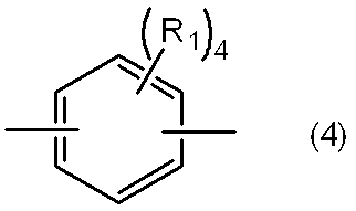
(式中、R1は各々独立に、水素原子、炭素数1~5の脂肪族炭化水素基、又はハロゲン原子を示す。)
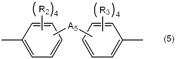
(式中、R2及びR3は各々独立に、水素原子、炭素数1~5の脂肪族炭化水素基、又はハロゲン原子を示し、A5は炭素数1~5のアルキレン基若しくはアルキリデン基、エーテル基、スルフィド基、スルフォニル基、カルボオキシ基、ケトン基、単結合、又は下記一般式(5-1)で表される残基である。)
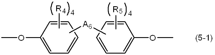
(式中、R4及びR5は各々独立に、水素原子、炭素数1~5の脂肪族炭化水素基、又はハロゲン原子を示し、A6は炭素数1~5のアルキレン基、イソプロピリデン基、エーテル基、スルフィド基、スルフォニル基、カルボオキシ基、ケトン基、又は単結合である。)

(式中、iは1~10の整数である。)
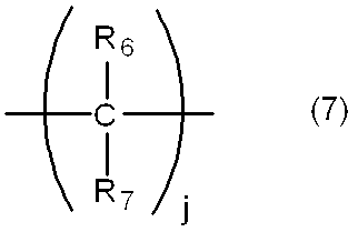
(式中、R6及びR7は各々独立に、水素原子又は炭素数1~5の脂肪族炭化水素基を示し、jは1~8の整数である。)
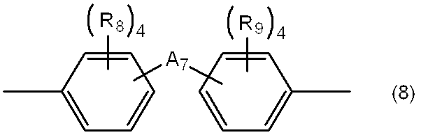
(式中、R8及びR9は各々独立に、水素原子、炭素数1~5の脂肪族炭化水素基、炭素数1~5のアルコキシ基、水酸基、又はハロゲン原子を示し、A7は炭素数1~5のアルキレン基若しくはアルキリデン基、エーテル基、スルフィド基、スルフォニル基、カルボオキシ基、ケトン基、フルオレニレン基、単結合、下記一般式(8-1)、又は下記一般式(8-2)で表される残基である。)

(式中、R10及びR11は各々独立に、水素原子、炭素数1~5の脂肪族炭化水素基、又はハロゲン原子を示し、A8は炭素数1~5のアルキレン基、イソプロピリデン基、m-又はp-フェニレンジイソプロピリデン基、エーテル基、スルフィド基、スルフォニル基、カルボオキシ基、ケトン基、又は単結合である。)

(式中、R12は各々独立に、水素原子、炭素数1~5の脂肪族炭化水素基、又はハロゲン原子を示し、A9及びA10は炭素数1~5のアルキレン基、イソプロピリデン基、エーテル基、スルフィド基、スルフォニル基、カルボオキシ基、ケトン基、又は単結合である。)
ポリイミド化合物(A)を製造する際に使用される有機溶媒は特に制限はなく、公知の溶媒を使用できる。有機溶媒は、後述する層間絶縁用樹脂フィルム用ワニスの製造に用いられる有機溶媒であってもよい。
また、この工程では前述の有機溶媒を追加又は濃縮して反応原料の固形分濃度、溶液粘度を調整することができる。反応原料の固形分濃度は、特に制限はないが、例えば、10~90質量%が好ましく、20~80質量%がより好ましい。反応原料の固形分濃度が10質量%以上の場合、反応速度が遅くなりすぎず、製造コストの面で有利である。また、反応原料の固形分濃度が90質量%以下の場合、より良好な溶解性が得られ、攪拌効率が良く、またゲル化することも少ない。
なお、ポリイミド化合物(A)の製造後に、目的に合わせて有機溶媒の一部又は全部を除去して濃縮してもよく、有機溶媒を追加して希釈してもよい。追加で使用される有機溶媒としては、ポリイミド化合物(A)の製造工程で例示した有機溶媒が適用できる。これらは1種類を単独で用いてもよく、2種類以上を混合して用いてもよい。また、使用する有機溶媒は、溶解性の観点から、メチルエチルケトン、シクロヘキサノン、プロピレングリコールモノメチルエーテル、N,N-ジメチルホルムアミド、N,N-ジメチルアセトアミドが好ましい。
本実施形態において、変性ポリブタジエン(B)は、化学変性されているポリブタジエンであれば、特に限定されない。変性ポリブタジエン(B)を用いると、得られる層間絶縁層において、無機充填材(C)と樹脂成分との分離、光沢ムラ等を低減できる。本明細書において、化学変性されているポリブタジエンとは、分子中の側鎖の1,2-ビニル基及び/又は末端の両方若しくは片方が、酸無水物化、エポキシ化、グリコール化、フェノール化、マレイン化、(メタ)アクリル化、ウレタン化等の化学変性されたものを指す。
変性ポリブタジエン(B)は、側鎖に1,2-ビニル基を有する1,2-ブタジエン単位を分子中に含有するものが好ましく、前記1,2-ブタジエン単位を40質量%以上含有するものがより好ましい。
より誘電正接が低い熱硬化性樹脂組成物を得る観点から、変性ポリブタジエン(B)は酸無水物で変性されているポリブタジエンが好ましい。酸無水物としては限定されないが、無水フタル酸、無水マレイン酸、無水トリメリット酸、無水ピロメリット酸、ヘキサヒドロ無水フタル酸、テトラヒドロ無水フタル酸、無水メチルナジック酸、無水ナジック酸、無水グルタル酸、無水ジメチルグルタル酸、無水ジエチルグルタル酸、無水コハク酸、メチルヘキサヒドロ無水フタル酸、メチルテトラヒドロ無水フタル酸等が挙げられ、無水フタル酸、無水マレイン酸、無水トリメリット酸、無水ピロメリット酸、ヘキサヒドロ無水フタル酸、テトラヒドロ無水フタル酸のいずれかであることが好ましく、無水マレイン酸がより好ましい。
変性ポリブタジエン(B)が酸無水物で変性されている場合、変性ポリブタジエン(B)1分子中に含まれる酸無水物由来の基(以下、「酸無水物基」ともいう)の数は、1~10が好ましく、1~6がより好ましく、2~5がさらに好ましい。酸無水物基の数が1分子中に1以上であると、層間絶縁層を形成した際の無機充填材(C)と樹脂成分との分離がより抑制される傾向にある。また、酸無水物基の数が1分子中に10以下であると、得られる熱硬化性樹脂組成物の誘電正接がより低くなる傾向にある。
すなわち、変性ポリブタジエン(B)が無水マレイン酸で変性されている場合、上記と同様の観点から、変性ポリブタジエン(B)1分子中に含まれる無水マレイン酸由来の基(以下、「無水マレイン酸基」ともいう)の数は、1~10が好ましく、1~6がより好ましく、2~5がさらに好ましい。
無機充填材(C)としては、特に限定されず、例えば、シリカ、アルミナ、硫酸バリウム、タルク、クレー、雲母粉、水酸化アルミニウム、水酸化マグネシウム、炭酸カルシウム、炭酸マグネシウム、酸化マグネシウム、窒化ホウ素、ホウ酸アルミニウム、チタン酸バリウム、チタン酸ストロンチウム、チタン酸カルシウム、チタン酸マグネシウム、チタン酸ビスマス、酸化チタン、ジルコン酸バリウム、ジルコン酸カルシウム等が挙げられる。得られる層間絶縁層をより低熱膨張化できる観点から、成分(C)は、シリカが好ましい。
成分(C)の体積平均粒径は、特に限定されないが、例えば、0.05~5μmが好ましく、0.1~3μmがより好ましく、0.2~1μmがさらに好ましい。成分(C)の体積平均粒径が5μm以下であれば、層間絶縁層上に回路パターンを形成する際にファインパターンの形成をより安定的に行える傾向にある。また、成分(C)の体積平均粒径が0.1μm以上であれば、耐熱性がより良好となる傾向にある。なお、体積平均粒径とは、粒子の全体積を100%として、粒子径による累積度数分布曲線を求めたときの体積50%に相当する点の粒径のことであり、レーザー回折散乱法を用いた粒度分布測定装置等で測定できる。
カップリング剤を用いる場合、その添加方式は、本実施形態の熱硬化性樹脂組成物中に成分(C)を配合した後、カップリング剤を添加する、いわゆるインテグラルブレンド処理方式であってもよいが、より効果的に成分(C)の特長を発現させる観点から、予め無機充填材にカップリング剤を乾式又は湿式で表面処理した無機充填材を使用する方式であってもよい。
また、成分(C)のスラリーの不揮発分濃度は特に制限はないが、例えば、無機充填材(C)の沈降性及び分散性の観点から、50~80質量%が好ましく、60~80質量%がより好ましい。
成分(C)の含有量は、例えば、熱硬化性樹脂組成物の樹脂成分の固形分換算100質量部に対して、40~300質量部が好ましく、60~200質量部がより好ましく、80~150質量部がさらに好ましい。
本実施形態の熱硬化性樹脂組成物に難燃剤を含有させることで、より良好な難燃性を付与することができる。難燃剤としては特に限定されず、例えば、塩素系難燃剤、臭素系難燃剤、リン系難燃剤、金属水和物系難燃剤等が挙げられる。環境への適合性からは、リン系難燃剤又は金属水和物系難燃剤が好ましい。
本実施形態の熱硬化性樹脂組成物に適切な硬化促進剤を含有させることで、熱硬化性樹脂組成物の硬化性を向上させ、層間絶縁層の誘電特性、耐熱性、高弾性率性、ガラス転移温度等をより向上させることができる。硬化促進剤としては、特に限定されず、例えば、各種イミダゾール化合物及びその誘導体;各種第3級アミン化合物、各種第4級アンモニウム化合物、トリフェニルホスフィン等の各種リン系化合物などが挙げられる。
本実施形態の熱硬化性樹脂組成物には、その他にも酸化防止剤、流動調整剤等の添加剤を含有させてもよい。
本実施形態の層間絶縁用樹脂フィルムは、第一の熱硬化性樹脂組成物を含むものである。
本実施形態の層間絶縁用樹脂フィルムは、そのいずれか一方の面に支持体が設けられたものであってもよい。
支持体としては、例えば、ポリエチレン、ポリプロピレン、ポリ塩化ビニル等のポリオレフィンのフィルム;ポリエチレンテレフタレート(以下、「PET」ともいう)、ポリエチレンナフタレート等のポリエステルのフィルム;ポリカーボネートフィルム、ポリイミドフィルム等の各種プラスチックフィルムなどが挙げられる。また、銅箔、アルミニウム箔等の金属箔、離型紙などを使用してもよい。支持体及び後述する保護フィルムには、マット処理、コロナ処理等の表面処理が施してあってもよい。また、支持体及び後述する保護フィルムには、シリコーン樹脂系離型剤、アルキッド樹脂系離型剤、フッ素樹脂系離型剤等による離型処理が施してあってもよい。
支持体の厚さは特に限定されないが、10~150μmが好ましく、25~50μmがより好ましい。
本実施形態の層間絶縁用樹脂フィルムは、例えば、次のようにして製造することができる。
まず、成分(A)、成分(B)、成分(C)及び必要に応じて使用されるその他の成分を有機溶媒に溶解又は分散した樹脂ワニス(以下、「層間絶縁用樹脂フィルム用ワニス」ともいう)の状態にすることが好ましい。
有機溶媒の配合量は、層間絶縁用樹脂フィルム用ワニスの全質量100質量部に対して、10~60質量部が好ましく、10~35質量部がより好ましい。
支持体に層間絶縁用樹脂フィルム用ワニスを塗工する方法としては、例えば、コンマコーター、バーコーター、キスコーター、ロールコーター、グラビアコーター、ダイコーター等の塗工装置を用いることができる。これらの塗工装置は、膜厚によって、適宜選択することが好ましい。
塗工後の乾燥条件は特に限定されないが、例えば、30~60質量%の有機溶媒を含む層間絶縁用樹脂フィルム用ワニスの場合、50~150℃で3~10分程度乾燥させることにより、層間絶縁用樹脂フィルムを好適に形成することができる。乾燥後の層間絶縁用樹脂フィルム中の揮発成分(主に有機溶媒)の含有量が、10質量%以下となるように乾燥させることが好ましく、6質量%以下となるように乾燥させることがより好ましい。
本実施形態の複合フィルムは、本実施形態の熱硬化性樹脂組成物を含む第一の樹脂層と、第二の樹脂層とを含む複合フィルムである。すなわち、本実施形態の複合フィルムは、第一の熱硬化性樹脂組成物及び後述の第二の熱硬化性樹脂組成物を含有することが好ましい。
なお、第一の樹脂層と第二の絶縁層との間には、明確な界面が存在せず、例えば、第一の樹脂層の構成成分の一部と、第二の絶縁層の構成成分の一部とが、相溶及び/又は混合した状態であってもよい。
第一の樹脂層は、本実施形態の第一の熱硬化性樹脂組成物を含むものである。第一の樹脂層は、例えば、本実施形態の複合フィルムを用いてプリント配線板を製造する場合において、回路基板と接着補助層との間に設けられ、回路基板の導体層とその上の層とを絶縁するために用いられる。また、第一の樹脂層は、回路基板にスルーホール、ビアホール等が存在する場合、それらの中に流動し、該ホール内を充填する役割も果たす。
第二の樹脂層は、後述する本実施形態のプリント配線板において、本実施形態の熱硬化性樹脂組成物を含む第一の樹脂層の硬化物と、導体層との間に位置し、導体層との接着性を向上させることを目的として設けられるものである。第二の樹脂層を設けることにより、平滑な表面が得られ、且つ、めっきにて形成される導体層ともより良好な接着強度が得られる。したがって、微細配線を形成する観点から、第二の樹脂層を設けることが好ましい。
多官能エポキシ樹脂(D)は、エポキシ基を2個以上有する樹脂であれば、特に限定されないが、例えば、ビスフェノールA型エポキシ樹脂、ビスフェノールF型エポキシ樹脂、ビスフェノールS型エポキシ樹脂、クレゾールノボラック型エポキシ樹脂、フェノールノボラック型エポキシ樹脂、ビフェニル型エポキシ樹脂、ナフトール型エポキシ樹脂、アントラセン型エポキシ樹脂、ジシクロペンタジエン型エポキシ樹脂、ナフタレン型エポキシ樹脂、アラルキルノボラック型エポキシ樹脂、フルオレン型エポキシ樹脂、キサンテン型エポキシ樹脂等が挙げられる。めっき銅との接着性の観点から、ビフェニル構造を有することが好ましく、ビフェニル構造を有する多官能エポキシ樹脂又はビフェニル構造を有するアラルキルノボラック型エポキシ樹脂がより好ましい。
なお、本明細書において、樹脂組成物に含まれる固形分とは、樹脂組成物を構成する成分から揮発性の成分を除外した残分を意味する。
活性エステル硬化剤(E)は、エステル基を1分子中に1個以上有し、エポキシ樹脂の硬化作用を有するものをいう。
活性エステル硬化剤(E)としては、特に制限はないが、例えば、脂肪族又は芳香族カルボン酸と脂肪族又は芳香族ヒドロキシ化合物とから得られるエステル化合物等が挙げられる。
これらの中でも、脂肪族カルボン酸、脂肪族ヒドロキシ化合物等から得られるエステル化合物は、脂肪族鎖を含むことにより有機溶媒への可溶性及びエポキシ樹脂との相溶性を高くできる傾向にある。
また、芳香族カルボン酸、芳香族ヒドロキシ化合物等から得られるエステル化合物は、芳香族環を有することで耐熱性を高められる傾向にある。
活性エステル硬化剤(E)としては、例えば、フェノールエステル化合物、チオフェノールエステル化合物、N-ヒドロキシアミンエステル化合物、複素環ヒドロキシ化合物のエステル化化合物等が挙げられる。
より具体的には、例えば、芳香族カルボン酸とフェノール性水酸基との縮合反応にて得られる芳香族エステルが挙げられ、ベンゼン、ナフタレン、ビフェニル、ジフェニルプロパン、ジフェニルメタン、ジフェニルエーテル、ジフェニルスルホン酸等の芳香環の水素原子の2~4個をカルボキシ基で置換したものから選ばれる芳香族カルボン酸成分と、前記した芳香環の水素原子の1個を水酸基で置換した1価フェノールと芳香環の水素原子の2~4個を水酸基で置換した多価フェノールとの混合物を原材料として、芳香族カルボン酸とフェノール性水酸基との縮合反応にて得られる芳香族エステル等が好ましい。すなわち、上記芳香族カルボン酸成分由来の構造単位と上記1価フェノール由来の構造単位と上記多価フェノール由来の構造単位とを有する芳香族エステルが好ましい。
成分(F)は、フェノール性水酸基を有するポリブタジエン変性されたポリアミド樹脂であれば、特に制限はないが、ジアミン由来の構造単位と、フェノール性水酸基を含有するジカルボン酸由来の構造単位と、フェノール性水酸基を含有しないジカルボン酸由来の構造単位と、両末端にカルボキシ基を有するポリブタジエン由来の構造単位とを有するものが好ましい。具体的には、下記一般式(i)で表される構造単位、下記一般式(ii)で表される構造単位、及び下記一般式(iii)で表される構造単位を有するものが好ましく挙げられる。

一般式(i)~(iii)中、R’はそれぞれ独立に、芳香族ジアミン又は脂肪族ジアミンに由来する2価の基を示し、一般式(iii)中、R’’は芳香族ジカルボン酸、脂肪族ジカルボン酸又は両末端にカルボキシ基を有するオリゴマーに由来する2価の基を示す。
一般式(i)~(iii)中に含まれる複数のR’同士は同一であっても異なっていてもよい。また、zが2以上の整数のとき、複数のR’’同士は同一であっても異なっていてもよい。
なお、一般式(i)~(iii)中、R’は、具体的には、後述する芳香族ジアミン又は脂肪族ジアミンに由来する2価の基であり、R’’は、後述する芳香族ジカルボン酸、脂肪族ジカルボン酸又は両末端にカルボキシ基を有するオリゴマーに由来する2価の基であることが好ましい。
前記芳香族ジアミンとしては、例えば、ジアミノベンゼン、ジアミノトルエン、ジアミノフェノール、ジアミノジメチルベンゼン、ジアミノメシチレン、ジアミノニトロベンゼン、ジアミノジアゾベンゼン、ジアミノナフタレン、ジアミノビフェニル、ジアミノジメトキシビフェニル、ジアミノジフェニルエーテル、ジアミノジメチルジフェニルエーテル、メチレンジアミン、メチレンビス(ジメチルアニリン)、メチレンビス(メトキシアニリン)、メチレンビス(ジメトキシアニリン)、メチレンビス(エチルアニリン)、メチレンビス(ジエチルアニリン)、メチレンビス(エトキシアニリン)、メチレンビス(ジエトキシアニリン)、イソプロピリデンジアニリン、ジアミノベンゾフェノン、ジアミノジメチルベンゾフェノン、ジアミノアントラキノン、ジアミノジフェニルチオエーテル、ジアミノジメチルジフェニルチオエーテル、ジアミノジフェニルスルホン、ジアミノジフェニルスルホキシド、ジアミノフルオレン等が挙げられる。
前記脂肪族ジアミンとしては、例えば、エチレンジアミン、プロパンジアミン、ヒドロキシプロパンジアミン、ブタンジアミン、へプタンジアミン、ヘキサンジアミン、シクロペンタンジアミン、シクロヘキサンジアミン、アザペンタンジアミン、トリアザウンデカジアミン等が挙げられる。
フェノール性水酸基を含有しないジカルボン酸としては、例えば、芳香族ジカルボン酸、脂肪族ジカルボン酸、両末端にカルボキシ基を有するオリゴマー等が挙げられる。
芳香族ジカルボン酸としては、例えば、フタル酸、イソフタル酸、テレフタル酸、ビフェニルジカルボン酸、メチレン二安息香酸、チオ二安息香酸、カルボニル二安息香酸、スルホニル安息香酸、ナフタレンジカルボン酸等が挙げられる。
脂肪族ジカルボン酸としては、例えば、シュウ酸、マロン酸、メチルマロン酸、コハク酸、グルタル酸、アジピン酸、マレイン酸、フマル酸、りんご酸、酒石酸、(メタ)アクリロイルオキシコハク酸、ジ(メタ)アクリロイルオキシコハク酸、(メタ)アクリロイルオキシりんご酸、(メタ)アクリルアミドコハク酸、(メタ)アクリルアミドりんご酸等が挙げられる。
第二の熱硬化性樹脂組成物は、更にリン系硬化促進剤(G)を含有することが好ましい。
リン系硬化促進剤(G)としては、リン原子を含有し、多官能エポキシ樹脂(D)と活性エステル硬化剤(E)との反応を促進させる硬化促進剤であれば特に制限なく使用することができる。
第二の熱硬化性樹脂組成物は、リン系硬化促進剤(G)を含有することによって、硬化反応をより一層十分に進めることができる。この理由は、リン系硬化促進剤(G)を用いることによって、活性エステル硬化剤(E)中のカルボニル基の電子求引性を高めることができ、これにより活性エステル硬化剤(E)と多官能エポキシ樹脂(D)との反応が促進されるためと推察される。
このように第二の熱硬化性樹脂組成物は、リン系硬化促進剤(G)を含有することにより、他の硬化促進剤を用いた場合より、多官能エポキシ樹脂(D)と活性エステル硬化剤(E)との硬化反応がより一層十分に進行するため、第一の樹脂層と組み合わせた際に、低い誘電正接が得られると考えられる。
第三ホスフィンとしては、特に限定されないが、例えば、トリノルマルブチルホスフィン、ジブチルフェニルホスフィン、ブチルジフェニルホスフィン、エチルジフェニルホスフィン、トリフェニルホスフィン、トリス(4-メチルフェニル)ホスフィン、トリス(4-メトキシフェニル)ホスフィン等が挙げられる。また、キノン類としては、例えば、o-ベンゾキノン、p-ベンゾキノン、ジフェノキノン、1,4-ナフトキノン、アントラキノン等が挙げられる。めっき銅との接着性、耐熱性、及び平滑な表面が得られる点から、例えば、トリノルマルブチルホスフィンとp-ベンゾキノンとの付加物がより好ましい。
第二の熱硬化性樹脂組成物は、充填材(H)を含有していてもよい。充填材(H)としては、無機充填材、有機充填材等が挙げられる。
充填材(H)を含有することで、第二の絶縁層をレーザー加工する際に樹脂の飛散をより低減できる。
無機充填材の粒子径は、第二の樹脂層上に微細配線を形成する観点から、比表面積が、20m2/g以上が好ましく、50m2/g以上がより好ましい。比表面積の上限に特に制限はないが、入手容易性の観点からは、500m2/g以下が好ましく、200m2/g以下がより好ましい。
比表面積は、不活性気体の低温低湿物理吸着によるBET法で求めることができる。具体的には、粉体粒子表面に、吸着占有面積が既知の分子を液体窒素温度で吸着させ、その吸着量から粉体粒子の比表面積を求めることができる。
比表面積が20m2/g以上の無機充填材としては、市販品を用いてもよい。市販品としては、例えば、ヒュームドシリカであるAEROSIL R972(日本アエロジル株式会社製、商品名、比表面積110±20m2/g)、及びAEROSIL R202(日本アエロジル株式会社製、商品名、比表面積100±20m2/g)、コロイダルシリカであるPL-1(扶桑化学工業株式会社製、商品名、比表面積181m2/g)、PL-7(扶桑化学工業株式会社製、商品名、比表面積36m2/g)等が挙げられる。また、耐湿性を向上させる観点からは、シランカップリング剤等の表面処理剤で表面処理された無機充填材であることが好ましい。
第二の熱硬化性樹脂組成物は、シアネート樹脂(J)を含有していてもよい。シアネート樹脂(J)は、特に限定されず、例えば、ビスフェノールA型、ビスフェノールF型、ビスフェノールS型等のビスフェノール型シアネート樹脂、フェノールノボラック型、アルキルフェノールノボラック型等のノボラック型シアネート樹脂、ジシクロペンタジエン型シアネート樹脂、及びこれらが一部トリアジン化したプレポリマーなどが挙げられる。これらのシアネート樹脂(J)は単独で又は2種以上を組み合わせて使用してもよい。
第二の熱硬化性樹脂組成物は、上記各成分の他に、本発明の効果を阻害しない範囲で、必要に応じて他の熱硬化性樹脂、熱可塑性樹脂、並びに難燃剤、酸化防止剤、流動調整剤、硬化促進剤等の添加剤などを含有することができる。
支持体としては、前記本実施形態の層間絶縁用樹脂フィルムに用いることができる支持体と同様のものが挙げられる。
本実施形態の複合フィルムは、例えば、前記支持体の上に第二の樹脂層を形成し、その上に第一の樹脂層を形成する方法により製造することができる。
第一の樹脂層の形成には、前述の第一の熱硬化性樹脂組成物又は層間絶縁用樹脂フィルム用ワニス(ここでは、「第一の樹脂層用ワニス」ともいう)を用いることができる。
第二の樹脂層の形成には、第二の熱硬化性樹脂組成物又は第二の熱硬化性樹脂組成物を有機溶媒に溶解又は分散した樹脂ワニス(以下、「第二の樹脂層用ワニス」ともいう)を用いることが好ましい。
第二の樹脂層用ワニスの製造方法、第二の樹脂層用ワニスの製造に用いる有機溶媒は、前記層間絶縁用樹脂フィルム用ワニスと同様である。
有機溶媒の配合量は、第二の樹脂層用ワニスの全質量100質量部に対して、70~95質量部が好ましく、80~90質量部がさらに好ましい。
なお、 本明細書において「ワニス」とは「有機溶媒を含有する樹脂組成物」と組成的に同義である。
第二の樹脂層用ワニス、又は第一の樹脂層用ワニスの塗工方法、及びこれらを塗工した後の乾燥条件は、本実施形態の層間絶縁用樹脂フィルムの製造方法における塗工方法、及び乾燥条件と同様である。
本実施形態のプリント配線板は、本実施形態の層間絶縁用樹脂フィルムの硬化物、又は本実施形態の複合フィルムの硬化物を含む。言い換えれば、本実施形態のプリント配線板は、層間絶縁層を有し、当該層間絶縁層のうち少なくとも一層が本実施形態の熱硬化性樹脂組成物を含む。
以下では、本実施形態の層間絶縁用樹脂フィルム又は複合フィルムを基材にラミネートし、プリント配線板を製造する方法について説明する。
工程(1):本実施形態の層間絶縁用樹脂フィルム又は複合フィルムを、基材の片面又は両面にラミネートする工程
工程(2):層間絶縁用樹脂フィルム又は複合フィルムを熱硬化し、層間絶縁層を形成する工程
工程(3):層間絶縁層を形成した基材に穴あけする工程
工程(4):層間絶縁層の表面を粗化処理する工程
工程(5):粗化された層間絶縁層の表面に導体層を形成する工程
工程(1)は、本実施形態の層間絶縁用樹脂フィルム又は複合フィルムを、基材の片面又は両面にラミネートする工程である。層間絶縁用樹脂フィルム又は複合フィルムをラミネートする装置としては、例えば、真空ラミネーターが挙げられる。真空ラミネーターとしては市販品を用いることができ、市販品の真空ラミネーターとしては、例えば、ニチゴー・モートン株式会社製のバキュームアップリケーター、株式会社名機製作所製の真空加圧式ラミネーター、日立インダストリーズ株式会社製のロール式ドライコーター、日立エーアイシー株式会社製の真空ラミネーター等が挙げられる。
複合フィルムを用いる場合、第一の樹脂層が、基材に対向するように配置する。
ラミネートの条件は、層間絶縁用樹脂フィルム又は複合フィルム、及び基材を必要に応じてプレヒートし、圧着温度(ラミネート温度)を60~140℃、圧着圧力を0.1~1.1mPa(9.8×10⁴~107.9×10⁴N/m2)、空気圧20mmHg(26.7hPa)以下の減圧下でラミネートしてもよい。また、ラミネートの方法は、バッチ式であっても、ロールでの連続式であってもよい。
工程(2)は、層間絶縁用樹脂フィルム又は複合フィルムを熱硬化し、層間絶縁層を形成する工程である。加熱硬化の条件は特に限定されないが、例えば、170~220℃で20~80分の範囲で選択することができる。層間絶縁用樹脂フィルム又は複合フィルムを熱硬化させた後に、支持体を剥離してもよい。
工程(3)として、層間絶縁層を形成した基材に穴あけする工程を行ってもよい。本工程では、層間絶縁層及び基材にドリル、レーザー、プラズマ、又はこれらの組み合わせ等の方法により、穴あけを行い、ビアホール、スルーホール等を形成する。レーザーとしては、炭酸ガスレーザー、YAGレーザー、UVレーザー、エキシマレーザー等が一般的に用いられる。
工程(4)は、層間絶縁層の表面を粗化処理する工程である。本工程では、工程(2)で形成した層間絶縁層の表面を酸化剤により粗化処理を行うと同時に、ビアホール、スルーホール等が形成されている場合には、これらを形成する際に発生する「スミア」の除去を行うこともできる。
酸化剤としては、特に限定されないが、例えば、過マンガン酸塩(過マンガン酸カリウム、過マンガン酸ナトリウム)、重クロム酸塩、オゾン、過酸化水素、硫酸、硝酸等が挙げられる。これらの中でも、ビルドアップ工法によるプリント配線板の製造における層間絶縁層の粗化に汎用されている酸化剤であるアルカリ性過マンガン酸溶液(例えば、過マンガン酸カリウム、過マンガン酸ナトリウム溶液)を用いて粗化、及びスミアの除去を行ってもよい。
工程(5)は、粗化された層間絶縁層の表面に導体層を形成する工程である。本工程では、例えば、サブトラクティブ法、セミアディティブ法等を用いてめっきにより回路を形成することができる。セミアディティブ法は、層間絶縁層の表面に無電解めっきにて給電層を形成し、次いで導体層とは逆パターンのめっきレジストを形成し、電解めっきにより導体層(回路)を形成する方法である。なお、導体層形成後、例えば、150~200℃で20~90分間アニール処理を施すことにより、層間絶縁層と導体層との接着強度を向上及び安定化させることができる。
<ポリイミド化合物(A)の製造>
温度計、還流冷却管、撹拌装置を備えた加熱及び冷却可能な容積1リットルのガラス製フラスコ容器に、3,3’-ジメチル-5,5’-ジエチル-4,4’-ジフェニルメタンビスマレイミド(大和化成工業株式会社製、商品名:BMI-5100)(成分(a1))114.8g、2,2-ビス(4-(4-マレイミドフェノキシ)フェニル)プロパン(大和化成工業株式会社製、商品名:BMI-4000)(成分(a1))345.5g、4,4’-[1,3-フェニレンビス(1-メチルエチリデン)]ビスアニリン(三井化学ファイン株式会社製、商品名:ビスアニリンM)(成分(a2))59.6g及びプロピレングリコールモノメチルエーテル280gを投入し、液温を120℃に保ったまま、撹拌しながら3時間反応させた。その後、ゲルパーミエーションクロマトグラフィー(GPC)により、反応物の重量平均分子量が900であることを確認し、冷却及び200メッシュ濾過してポリイミド化合物(A)(固形分濃度65質量%)を製造した。
得られたポリイミド化合物(A)の重量平均分子量は、GPCにより、標準ポリスチレンを用いた検量線から換算した。検量線は、標準ポリスチレン:TSKstandard POLYSTYRENE(Type;A-2500、A-5000、F-1、F-2、F-4、F-10、F-20、F-40)[東ソー株式会社製、商品名]を用いて3次式で近似した。GPCの条件は、以下に示す。
装置:(ポンプ:L-6200型[株式会社日立ハイテクノロジーズ製])
(検出器:L-3300型RI[株式会社日立ハイテクノロジーズ製])
(カラムオーブン:L-655A-52[株式会社日立ハイテクノロジーズ製])
カラム:ガードカラム;TSK Guardcolumn HHR-L + カラム;TSK gel-G4000HHR+TSK gel-G2000HHR(すべて東ソー株式会社製、商品名)
カラムサイズ:6.0×40mm(ガードカラム)、7.8×300mm(カラム)
溶離液:テトラヒドロフラン
試料濃度:30mg/5mL
注入量:20μL
流量:1.00mL/分
測定温度:40℃
実施例1
無機充填材(C)としてアミノシランカップリング剤処理を施したシリカ(株式会社アドマテックス製、商品名:SC-2050-KNK、固形分濃度70質量%のメチルイソブチルケトン分散液)と、変性ポリブタジエン(B)として変性ポリブタジエン(クレイバレー社製、商品名:Ricon130MA8)とを、無機充填材(C)の含有量が、有機溶媒を含まない層間絶縁用樹脂フィルムの全質量中、54質量%となり、変性ポリブタジエン(B)の含有量が、層間絶縁用樹脂フィルムに含まれる全樹脂成分中20質量%となる配合比率で、混合した。
そこに製造例1で製造したポリイミド化合物(A)を、ポリイミド化合物(A)の含有量が、層間絶縁用樹脂フィルムに含まれる全樹脂成分中80質量%となる比率で混合し、高速回転ミキサーにより室温で溶解させた。
ポリイミド化合物(A)が溶解したことを目視で確認した後、硬化促進剤として、イソシアネートマスクイミダゾール(第一工業製薬株式会社製、商品名:G8009L)を、ポリイミド化合物(A)の仕込み量から換算される原料の成分(a1)に対して0.3phr混合した。次いで、ナノマイザー処理によって分散し、層間絶縁用樹脂フィルムを作製するためのワニス1を得た。
次に、このワニス1を、支持体であるPETフィルム(厚さ38μm)上に、乾燥後の層間絶縁用樹脂フィルムの厚さが37μmとなるようにコンマコーターを用いて塗布した後、85℃で2分間乾燥した。なお、乾燥後の層間絶縁用樹脂フィルム中の揮発成分の量は6質量%であった。次いで、層間絶縁用樹脂フィルムの表面に保護フィルムとして厚さ15μmのポリプロピレンフィルムを貼り合わせながらロール状に巻き取り、支持体及び保護フィルムを有する層間絶縁用樹脂フィルム1を得た。
各成分及びその配合量を表1に示す配合に変更した以外は実施例1と同様にして、層間絶縁用樹脂フィルムを作製するためのワニス2~6を得た。次に、このワニス2~6を使用して、実施例1と同様にして、支持体及び保護フィルムを有する層間絶縁用樹脂フィルム2~6を得た。
実施例4
<ビスフェノールAジシアネートのプレポリマーの合成>
容積1リットルのセパラブルフラスコにトルエン269.6g、2,2-ビス(4-シアナトフェニル)プロパン(ロンザジャパン株式会社製、商品名:PrimasetBADCY)620.4g、p-(α-クミル)フェノール(東京化成工業株式会社製)9.5gを投入した。2,2-ビス(4-シアナトフェニル)プロパンとp-(α-クミル)フェノールとがトルエンに溶解したことを目視にて確認した後、液温を100℃に保ち、反応促進剤として反応溶媒(本検討ではトルエン)に対して10質量%に希釈したナフテン酸亜鉛(和光純薬工業株式会社製)0.46gを配合し、窒素雰囲気下において100℃で3時間反応させて、ビスフェノールAジシアネートのプレポリマー溶液(固形分濃度70質量%)を製造した。上記の反応は、E型粘度計を用いて測定した25℃での反応溶液の粘度が70~90mPa・sの範囲となったときを終点とした。
上記で得られたビスフェノールAジシアネートのプレポリマー32.2質量部(固形分)、ナフタレンクレゾールノボラック型エポキシ樹脂(日本化薬株式会社製、商品名:NC-7000L、エポキシ当量231g/mol)42.8質量部、無機充填材(日本アエロジル株式会社製、商品名:アエロジルR972、比表面積110m2/g)8.8質量部、溶剤として、ジメチルアセトアミドを全質量(有機溶媒を含む)100質量部に対して86.5質量部配合し、目視にて樹脂成分の溶解が確認されるまで、室温で撹拌した。その後、ナノマイザー処理によって分散し、第二の樹脂層用ワニス1を得た。
実施例1と同様の方法により、層間絶縁用樹脂フィルムを作製するためのワニス1を作製し、第一の樹脂層用ワニス1とした。
第二の樹脂層用ワニス1を支持体であるPETフィルム(厚さ38μm)上に、乾燥後の第二の樹脂層の厚さが3μmとなるようにコンマコーターを用いて塗布し、140℃で3分間乾燥してPETフィルム上に第二の樹脂層を形成した。次いで、上記で得られた第二の樹脂層の上に第一の樹脂層用ワニス1を、乾燥後の第一の樹脂層の厚さが40μmとなるようにコンマコーターを用いて塗布し、85℃で2分間乾燥した。次いで、複合フィルムの第二の樹脂層が設けられていない面に、保護フィルムとして厚さ15μmのポリプロピレンフィルムを貼り合わせながらロール状に巻き取り、支持体及び保護フィルムを有する複合フィルム1を得た。
誘電正接の測定に用いた樹脂板は、以下の手順により作製した。
(I)実施例1~3、及び比較例1~3で得られた支持体及び保護フィルムを有する層間絶縁用樹脂フィルムから保護フィルムを剥離した後、110℃で3分間乾燥した。
次に、乾燥後の支持体を有する層間絶縁用樹脂フィルムを、真空加圧式ラミネーター(株式会社名機製作所製、商品名:MVLP-500/600-II)を用いて、銅箔(電界銅箔、厚さ35μm)の光沢面上に、層間絶縁用樹脂フィルムと銅箔とが当接するようにラミネートして、銅箔、層間絶縁用樹脂フィルム、支持体がこの順に積層された積層体(P)を得た。前記ラミネートは、30秒間減圧して圧力を0.5MPaとした後、130℃、30秒間、圧着圧力0.5MPaでプレスする方法により行った。その後、積層体(P)から支持体を剥離した。
(II)次に、支持体としてのPETフィルム及び保護フィルムとしてのポリプロピレンフィルムを有する層間絶縁用樹脂フィルムを準備し、保護フィルムを剥離した後、110℃で3分間の乾燥を行った。
(III)次に、上記(I)で得られた支持体を剥離した積層体(P)と、上記(II)で得られた乾燥後の支持体を有する層間絶縁用樹脂フィルムとを、層間絶縁用樹脂フィルム同士が当接するように、前記(I)と同様の条件でラミネートして、銅箔、層間絶縁用樹脂フィルム2層からなる層、支持体がこの順に積層された積層体(Q)を得た。その後、積層体(Q)から支持体を剥離した。
(IV)次に、上記(III)で得られた支持体を剥離した積層体(Q)と、上記(II)と同様の方法により得られた乾燥後の支持体を有する層間絶縁用樹脂フィルムとを、層間絶縁用樹脂フィルム同士が当接するように、前記(I)と同様の条件でラミネートして、銅箔、層間絶縁用樹脂フィルム3層からなる層、支持体がこの順に積層された積層体(R)を得た。
(V)前記(I)~(III)と同様の方法により、積層体(Q)を作製した。
(VI)上記(V)で得られた積層体(Q)と、上記(I)~(IV)で得られた積層体(R)の支持体をそれぞれ剥離し、積層体(Q)と積層体(R)の層間絶縁用樹脂フィルム同士を貼り合わせ、圧着圧力3.0MPaで190℃、60分間、真空プレスを用いてプレス成型を行った。得られた両面銅箔付き樹脂板を、190℃で2時間硬化させた後、過硫酸アンモニウムで銅箔をエッチングすることで、樹脂板を得た。
上記で作製された樹脂板を幅2mm、長さ70mmの試験片に切り出し、ネットワークアナライザー(アジレント・テクノロジー株式会社製、商品名:E8364B)と5GHz対応空洞共振器(株式会社関東電子応用開発製)を用いて、誘電正接を測定した。測定温度は25℃とした。評価結果を表1に示す。誘電正接が低いほど、誘電特性に優れることを示す。
実施例1~3、比較例1~3で得られた支持体及び保護フィルムを有する層間絶縁用樹脂フィルムの取り扱い性は、以下に示す方法で評価した。
(1)カッターでの切断による評価
上記で作製した支持体及び保護フィルムを有する層間絶縁用樹脂フィルムをカッターで切断した際の粉落ちの有無を評価した。粉落ちの有無は、目視で確認し、粉落ちしないものを取り扱い性良好とした。
(2)折り曲げによる評価
上記で作製した支持体及び保護フィルムを有する層間絶縁用樹脂フィルムの保護フィルムを剥離し、支持体から樹脂塗工面に向かって180°折り曲げたときの、フィルムの割れの有無を評価した。フィルムの割れの有無は、目視で確認し、割れが発生しないものを取り扱い性良好とした。
上記(1)及び(2)の評価において、どちらも取り扱い性良好となったものを「A」、それ以外を「B」とした。評価結果を表1に示す。
樹脂分離の有無はプリント配線板上に形成した層間絶縁層の断面を走査型電子顕微鏡(SEM)により観察することで確認した。実施例1~3、比較例1~3で得られた支持体及び保護フィルムを有する層間絶縁用樹脂フィルムの保護フィルムを剥離し、CZ処理が施されたプリント配線板(積層板として、日立化成株式会社製、商品名:MCL-E-700GRを使用した)上に、層間絶縁用樹脂フィルムとプリント配線板とが当接するようにラミネートした。ラミネートは、30秒間減圧して圧力を0.5MPaとし、その後、130℃、30秒間、圧着圧力0.5MPaでプレスする方法により行った。その後、室温に冷却し、支持体を剥離除去し、層間絶縁用樹脂フィルムを配したプリント配線板を得た。次に、該プリント配線板を190℃で60分間、防爆乾燥機中で加熱し、層間絶縁層が形成されたプリント配線板を得た。得られたプリント配線板の層間絶縁層の断面を電界放出型走査型電子顕微鏡(株式会社日立製作所製、商品名:S-4700)にて観察し、樹脂分離の有無を確認した。なお、電界放出型走査型電子顕微鏡の観察は、加速電圧10V、エミッション電流10μAで行った。実施例1~3及び比較例1~3で得られた層間絶縁層の断面SEM写真を図2に示す。層間絶縁層の断面SEM写真において、樹脂分離が確認されたものを「あり」、樹脂分離が確認されなかったものを「なし」とした。この評価においては、「なし」であることが好ましい。評価結果を表1に示す。
層間絶縁層の表面光沢ムラの評価は目視により評価した。実施例1~3、比較例1~3で得られた支持体及び保護フィルムを有する層間絶縁用樹脂フィルムの保護フィルムを剥離し、CZ処理が施されたプリント配線板(積層板として、日立化成株式会社製、商品名:MCL-E-700GRを使用した)上に、層間絶縁用樹脂フィルムとプリント配線板とが当接するようにラミネートした。ラミネートは、30秒間減圧して圧力を0.5MPaとし、その後、130℃、30秒間、圧着圧力0.5MPaでプレスする方法により行った。その後、室温に冷却し、支持体を剥離し、層間絶縁用樹脂フィルムを配したプリント配線板を得た。次に、該プリント配線板を190℃で60分間、防爆乾燥機中で硬化を行い、層間絶縁層が形成されたプリント配線板を得た。光沢ムラは、得られたプリント配線板の層間絶縁層表面を目視により観察し、層間絶縁層表面に樹脂の分離等がなく、均一な外観のものを「なし」、分離等があり、不均一な外観のものを「あり」とした。この光沢ムラの評価においては、「なし」であることが好ましい。評価結果を表1に示す。
表面粗さを測定するにあたり、以下の手順により表面粗さ測定用基板を作製した。
実施例4で得られた支持体及び保護フィルムを有する複合フィルムを、250mm×250mmのサイズに切断した後、保護フィルムを剥離した。
得られた支持体を有する複合フィルムを、CZ処理が施されたプリント配線板(積層板として、日立化成株式会社製、商品名:MCL-E-700GRを使用した)上に、第一の樹脂層とプリント配線板とが当接するようにラミネートした。ラミネートは、30秒間減圧して圧力を0.5MPaとし、その後、130℃、30秒間、圧着圧力0.5MPaでプレスする方法により行った。
その後、室温に冷却し、支持体を剥離し、複合フィルムを配したプリント配線板を得た。次に、複合フィルムを配したプリント配線板を190℃で60分間、防爆乾燥機中で硬化を行い、層間絶縁層が形成されたプリント配線板を得た。該プリント配線板を30mm×40mmに切り出したものを試験片とした。
上記で得られた試験片を、60℃に加温した膨潤液(ローム・アンド・ハース電子材料株式会社製、商品名:CIRCUPOSITMLB CONDITIONER211)に10分間浸漬処理した。次に、80℃に加温した粗化液(ローム・アンド・ハース電子材料株式会社製、商品名:CIRCUPOSITMLB PROMOTER213)に10分間浸漬処理した。引き続き、45℃に加温した中和液(ローム・アンド・ハース電子材料株式会社製、商品名:CIRCUPOSITMLB NEUTRALIZER MLB216)に5分間浸漬処理して中和した。このようにして、前記試験片の層間絶縁層の表面を粗化処理したものを、表面粗さ測定用基板として用いた。
めっき銅との接着強度を測定するにあたり、以下の手順によりめっき銅との接着強度測定用基板を作製した。
まず、前記表面粗さ測定用基板を30mm×40mmに切り出し、試験片とした。
該試験片を、60℃のアルカリクリーナー(アトテックジャパン株式会社製、商品名:クリーナーセキュリガント902)で5分間処理し、脱脂洗浄した。洗浄後、23℃のプリディップ液(アトテックジャパン株式会社製、商品名:プリディップネオガントB)で2分間処理した。その後、40℃のアクチベーター液(アトテックジャパン株式会社製、商品名:アクチベーターネオガント834)で5分間処理を施し、パラジウム触媒を付着させた。次に、30℃の還元液(アトテックジャパン株式会社製、商品名:リデューサーネオガントWA)で5分間処理した。
上記の処理を行った試験片を、化学銅液(アトテックジャパン株式会社製、商品名:ベーシックプリントガントMSK-DK)に入れ、層間絶縁層上のめっき厚さが0.5μmになるまで、無電解めっきを行った。無電解めっき後に、めっき皮膜中に残存している応力を緩和し、残留している水素ガスを除去するために、120℃で15分間ベーク処理を施した。
次に、無電解めっき処理された試験片に対して、さらに層間絶縁層上のめっき厚さが30μmになるまで、電解めっきを行い、導体層として銅層を形成した。電解めっき後、190℃で120分間加熱、硬化させて接着強度測定部作製前の測定基板を得た。
得られた測定基板の銅層に10mm幅のレジストを形成し、過硫酸アンモニウムで銅層をエッチングすることにより、接着強度測定部として10mm幅の銅層を有する、めっき銅との接着強度測定用基板を得た。
接着強度測定部の銅層の一端を、銅層と層間絶縁層との界面で剥がしてつかみ具でつかみ、小型卓上試験機(株式会社島津製作所製、商品名:EZTTest)を用いて、垂直方向に引っ張り速度50mm/分、室温中で引き剥がしたときの荷重を測定した。評価結果を表2に示す。
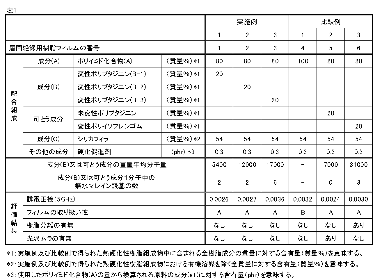
[変性ポリブタジエン(B)]
(B-1)Ricon130MA8(クレイバレー社製、商品名):重量平均分子量5400、1分子中の無水マレイン酸基の数2
(B-2)Ricon131MA5(クレイバレー社製、商品名):重量平均分子量12000、1分子中の無水マレイン酸基の数2
(B-3)Ricon184MA6(クレイバレー社製、商品名):重量平均分子量17000、1分子中の無水マレイン酸基の数6
[未変性ポリブタジエン]
Ricon181(クレイバレー社製、商品名):重量平均分子量7000、1分子中の無水マレイン酸基の数0
[変性ポリイソプレンゴム]
ポリイソプレンゴム(株式会社クラレ製、商品名:LIR-403):重量平均分子量31000、1分子中の無水マレイン酸基の数3
一方で、比較例1~3の層間絶縁用樹脂フィルムは、いずれかの特性で実施例に劣ることがわかる。
すなわち、本実施形態の熱硬化性樹脂組成物を用いて得られた本実施形態の層間絶縁用樹脂フィルムは、フィルムの取り扱い性に優れるものであり、本実施形態の層間絶縁用樹脂フィルムから得られる層間絶縁層は、樹脂分離及び光沢ムラが少なく、誘電正接が低いことがわかる。

<第一の樹脂層用ワニス2の製造>
無機充填材(C)としてアミノシランカップリング剤処理を施したシリカフィラー(株式会社アドマテックス製、商品名:SC-2050-KNK、固形分濃度70質量%のメチルイソブチルケトン分散液)68.3質量部と、変性ポリブタジエン(B)として、変性ポリブタジエン(クレイバレー社製、商品名:Ricon130MA8、重量平均分子量:5,400、1分子鎖中の無水マレイン酸基の数2)6.0質量部とを混合した。
そこに製造例1で製造したポリイミド化合物(A)を24.1質量部混合し、高速回転ミキサーにより室温で溶解させた。
その後、難燃剤(大八化学工業株式会社製、商品名:PX-200)を1.4質量部、イミダゾール系硬化促進剤(第一工業製薬株式会社製、商品名:G-8009L)を、ポリイミド化合物(A)の仕込み量から換算される原料の成分(a1)及び成分(a2)の合計量に対して0.5phr混合した後、ナノマイザー処理によって分散し、第一の樹脂層用ワニス2を得た。
成分(D)としてアラルキルノボラック型エポキシ樹脂(日本化薬株式会社製、商品名:NC-3000H、エポキシ当量289g/mol)42.0質量部、成分(H)として無機充填材(日本アエロジル株式会社製、商品名:アエロジルR972、比表面積110±20m2/g)8.8質量部、酸化防止剤(株式会社エーピーアイコーポレーション製、商品名:ヨシノックスBB)0.3質量部、溶剤として、DMAc(株式会社ゴードー製)を固形分濃度が40質量%になるように配合し、目視にて樹脂成分の溶解が確認されるまで、室温で攪拌した。その後、成分(F)として、あらかじめDMAcに固形分濃度が7質量%になるように溶解させたフェノール性水酸基含有ポリブタジエン変性ポリアミド樹脂(日本化薬株式会社製、商品名:BPAM-155)を固形分換算で6.4質量部、フェノキシ樹脂(三菱化学株式会社製、商品名:YX7200、メチルエチルケトン希釈品(35質量%))を固形分換算で9.1質量部、成分(E)として活性エステル硬化剤(DIC株式会社製、商品名:HPC-8000-65T(トルエン希釈品(65質量%)))を固形分換算で32.4質量部、レベリング剤(ビックケミージャパン社製、商品名:BYK-310(トルエン希釈品(25質量%)))を固形分換算で0.1質量部、成分(G)としてリン系硬化促進剤(トリノルマルブチルホスフィンとp-ベンゾキノンとの付加物)を0.8質量部配合し、固形分濃度が20質量%になるようDMAcで希釈した。その後、ナノマイザー処理によって分散し、第二の樹脂層用ワニス2を得た。
上記で得た第二の樹脂層用ワニス2を、離型処理された支持体(PETフィルム、東レフィルム加工株式会社製、商品名:セラピールSY(RX)(厚さ38μm))に、乾燥後の接着補助フィルムの厚さが3μmとなるようにコンマコーターを用いて塗布し、140℃で3分間乾燥して、支持体上に第二の樹脂層を形成した。次いで、該第二の樹脂層の上に、第一の樹脂層用ワニス2を、乾燥後の第一の樹脂層の厚さが40μmとなるようにコンマコーターを用いて塗布し、90℃で2分間乾燥した。次いで、第一の樹脂層の表面に、保護フィルムとして厚さ15μmのポリプロピレンフィルムを貼り合わせながらロール状に巻き取り、支持体及び保護フィルムを有する複合フィルム2を得た。
上記で得た支持体及び保護フィルムを有する複合フィルム2から保護フィルムを剥離した。得られた支持体を有する複合フィルムを、CZ処理が施されたプリント配線板(積層板として、日立化成株式会社製、商品名:MCL-E-700GRを使用した)上に、第一の樹脂層とプリント配線板とが当接するようにラミネートした。ラミネートは、100℃で30秒間真空引きした後、0.5MPaで30秒間加圧し、その後、100℃で60秒間、圧着圧力0.5MPaでプレスする方法により行った。室温に冷却した後、支持体を剥離し、複合フィルムを配したプリント配線板を得た。次に、該プリント配線板を190℃で60分間、防爆乾燥機中で硬化を行い、層間絶縁層が形成されたプリント配線板5Aを得た。
次に、プリント配線板5Aの表面を化学粗化するために、膨潤液として、ジエチレングリコールモノブチルエーテルを200ml/L及びNaOHを5g/L含む水溶液を作製し、60℃に加温した該水溶液中に、プリント配線板5Aを5分間浸漬処理した。次に、粗化液として、KMnO4を60g/L及びNaOHを40g/L含む水溶液を作製し、80℃に加温した該水溶液中に、膨潤液で処理した後のプリント配線板を5分間浸漬処理した。引き続き、中和液として、SnCl2を30g/L、HClを300ml/L含む水溶液を作製し、40℃に加温した該水溶液中に、粗化液で処理した後のプリント配線板を5分間浸漬処理し、KMnO4を還元して、化学粗化したプリント配線板5Bを得た。
次に、回路層を形成するために、化学粗化したプリント配線板5Bを、PdCl2を含む無電解めっき用触媒であるアクチベーターネオガント834(アトテックジャパン株式会社製、商品名)に35℃で5分間浸漬処理した。次いで、無電解銅めっき用であるめっき液プリントガントMSK-DK(アトテックジャパン株式会社製、商品名)に30℃で20分間浸漬し、さらに硫酸銅電解めっきを行った。その後、190℃で120分間アニール処理を行い、厚さ20μmの回路層を有するプリント配線板5Cを得た。
<第二の樹脂層用ワニス3の製造>
実施例5において、第二の樹脂層用ワニスの調製で用いたリン系硬化促進剤を、トリス(4-メチルフェニル)ホスフィンとp-ベンゾキノンとの付加物に変えた以外は、実施例5と同様にして第二の樹脂層用ワニス3を得た。
<複合フィルム及びプリント配線板の製造>
第一の樹脂層用ワニス2と、第二の樹脂層用ワニス3を用いて、実施例5と同様にして、複合フィルム3及びプリント配線板6A、6B及び6Cを得た。
実施例5及び6で作製した複合フィルムを用いて、実施例1~3と同様にして樹脂板を作製し、実施例1~3と同様の測定条件で誘電正接を測定した。結果を表3に示す。
実施例5及び6で作製したプリント配線板5B及び6Bの層間絶縁層の表面粗さを、実施例4と同様の測定条件で測定した。結果を表3に示す。
実施例5及び6で作製したプリント配線板5C及び6Cの導体層に、実施例4と同様の方法により、1cm幅の回路層を形成し、実施例4と同様の測定条件でめっき銅との接着強度(めっきピール強度)を測定した。結果を表3に示す。
実施例5及び6で作製したプリント配線板5C及び6Cを2cm×2cmに切断し、288℃の溶融はんだに浮かべた。その後、目視により膨れが確認されるまでの時間を測定した。結果を表3に示す。
実施例5及び6で作製したプリント配線板5B及び6Bの表面粗化形状を走査型電子顕微鏡(株式会社日立製作所製、商品名:S-4700)を使用して観察した。サンプルは前処理として白金蒸着処理を施し、加速電圧10kV、傾斜角度30°、二次電子像モードの条件で行った。得られた表面SEM写真を図3に示す。

2 第二の樹脂層
3 支持体
4 保護フィルム
Claims (14)
- N-置換マレイミド基を少なくとも2個有するマレイミド化合物(a1)由来の構造単位とジアミン化合物(a2)由来の構造単位とを有するポリイミド化合物(A)、変性ポリブタジエン(B)、及び無機充填材(C)を含有する、熱硬化性樹脂組成物。
- 変性ポリブタジエン(B)の重量平均分子量が、500~25000である、請求項1に記載の熱硬化性樹脂組成物。
- 変性ポリブタジエン(B)が無水マレイン酸で変性されたポリブタジエンである、請求項1又は2に記載の熱硬化性樹脂組成物。
- 変性ポリブタジエン(B)に含まれる無水マレイン酸由来の基の数が1分子中1~10である、請求項3に記載の熱硬化性樹脂組成物。
- ポリイミド化合物(A)の重量平均分子量が800~1500である、請求項1~4のいずれか1項に記載の熱硬化性樹脂組成物。
- 無機充填材(C)がシリカである、請求項1~5のいずれか1項に記載の熱硬化性樹脂組成物。
- 請求項1~6のいずれか1項に記載の熱硬化性樹脂組成物を含む、層間絶縁用樹脂フィルム。
- 請求項1~6のいずれか1項に記載の熱硬化性樹脂組成物を含む第一の樹脂層と、第二の樹脂層とを含む、複合フィルム。
- 前記第二の樹脂層が、多官能エポキシ樹脂(D)、活性エステル硬化剤(E)、及びフェノール性水酸基含有ポリブタジエン変性ポリアミド樹脂(F)を含有する第二の熱硬化性樹脂組成物を含む、請求項8に記載の複合フィルム。
- 前記第二の熱硬化性樹脂組成物中の多環能エポキシ樹脂(D)のエポキシ基に対する、活性エステル硬化剤(E)のエステル基の当量比(エステル基/エポキシ基)が0.3~1.5となる、請求項9に記載の複合フィルム。
- 前記第二の熱硬化性樹脂組成物が、更にリン系硬化促進剤(G)を含有する、請求項9又は10に記載の複合フィルム。
- 硬化物の5GHzの誘電正接が0.005以下である、請求項8~11のいずれか1項に記載の複合フィルム。
- 請求項7に記載の層間絶縁用樹脂フィルム、又は請求項8~12のいずれか1項に記載の複合フィルムの硬化物を含む、プリント配線板。
- 請求項7に記載の層間絶縁用樹脂フィルム、又は請求項8~12のいずれか1項に記載の複合フィルムを、基材の片面又は両面にラミネートする工程を備える、プリント配線板の製造方法。
Priority Applications (4)
| Application Number | Priority Date | Filing Date | Title |
|---|---|---|---|
| US15/543,508 US10544305B2 (en) | 2015-01-16 | 2015-12-03 | Thermosetting resin composition, resin film for interlayer insulation, composite film, printed wiring board, and method for producing same |
| KR1020177019155A KR102375044B1 (ko) | 2015-01-16 | 2015-12-03 | 열경화성 수지 조성물, 층간 절연용 수지 필름, 복합 필름, 프린트 배선판 및 그의 제조 방법 |
| JP2016569255A JP6903915B2 (ja) | 2015-01-16 | 2015-12-03 | 熱硬化性樹脂組成物、層間絶縁用樹脂フィルム、複合フィルム、プリント配線板及びその製造方法 |
| CN201580073082.5A CN107109055B (zh) | 2015-01-16 | 2015-12-03 | 热固性树脂组合物、层间绝缘用树脂膜、复合膜、印刷布线板及其制造方法 |
Applications Claiming Priority (2)
| Application Number | Priority Date | Filing Date | Title |
|---|---|---|---|
| JP2015-006333 | 2015-01-16 | ||
| JP2015006333 | 2015-01-16 |
Publications (1)
| Publication Number | Publication Date |
|---|---|
| WO2016114030A1 true WO2016114030A1 (ja) | 2016-07-21 |
Family
ID=56405586
Family Applications (1)
| Application Number | Title | Priority Date | Filing Date |
|---|---|---|---|
| PCT/JP2015/084038 Ceased WO2016114030A1 (ja) | 2015-01-16 | 2015-12-03 | 熱硬化性樹脂組成物、層間絶縁用樹脂フィルム、複合フィルム、プリント配線板及びその製造方法 |
Country Status (6)
| Country | Link |
|---|---|
| US (1) | US10544305B2 (ja) |
| JP (2) | JP6903915B2 (ja) |
| KR (1) | KR102375044B1 (ja) |
| CN (1) | CN107109055B (ja) |
| TW (1) | TWI696661B (ja) |
| WO (1) | WO2016114030A1 (ja) |
Cited By (6)
| Publication number | Priority date | Publication date | Assignee | Title |
|---|---|---|---|---|
| JP2018012748A (ja) * | 2016-07-19 | 2018-01-25 | 日立化成株式会社 | 半導体再配線層形成用樹脂フィルム、半導体再配線層形成用複合フィルム、それらを用いた半導体装置及び半導体装置の製造方法 |
| TWI631194B (zh) * | 2016-12-07 | 2018-08-01 | 日立化成股份有限公司 | 樹脂清漆、預浸體、積層板及印刷線路板 |
| WO2018168718A1 (ja) * | 2017-03-14 | 2018-09-20 | 三井金属鉱業株式会社 | 樹脂組成物、樹脂付銅箔、誘電体層、銅張積層板、キャパシタ素子及びキャパシタ内蔵プリント配線板 |
| JP2019014799A (ja) * | 2017-07-05 | 2019-01-31 | 日立化成株式会社 | 樹脂組成物、樹脂付キャリアフィルム、絶縁樹脂付キャリアフィルム、めっきプロセス用プライマー層、めっきプロセス用プライマー層付キャリアフィルム、配線板及び配線板の製造方法 |
| CN110785399A (zh) * | 2017-06-28 | 2020-02-11 | Dic株式会社 | 活性酯组合物和半导体密封材料 |
| US20220276558A1 (en) * | 2019-08-14 | 2022-09-01 | Showa Denko Materials Co., Ltd. | Photosensitive resin composition, photosensitive resin film, multilayer printed wiring board, semiconductor package, and production method for multilayer printed wiring board |
Families Citing this family (20)
| Publication number | Priority date | Publication date | Assignee | Title |
|---|---|---|---|---|
| CN109476124B (zh) * | 2016-08-09 | 2021-06-22 | 东洋纺株式会社 | 含有低介电粘合剂层的层叠体 |
| TWI899456B (zh) * | 2016-09-26 | 2025-10-01 | 日商力森諾科股份有限公司 | 樹脂組成物、半導體用配線層積層體及半導體裝置 |
| JP6553311B2 (ja) | 2017-01-10 | 2019-07-31 | 住友精化株式会社 | エポキシ樹脂組成物 |
| JP7069561B2 (ja) * | 2017-04-10 | 2022-05-18 | 昭和電工マテリアルズ株式会社 | 積層板の製造方法、プリント配線板の製造方法、及び半導体パッケージの製造方法 |
| JP7081127B2 (ja) * | 2017-12-05 | 2022-06-07 | 昭和電工マテリアルズ株式会社 | 熱硬化性樹脂組成物、プリプレグ、積層板、プリント配線板及び高速通信対応モジュール |
| JP7176186B2 (ja) * | 2017-12-05 | 2022-11-22 | 昭和電工マテリアルズ株式会社 | 熱硬化性樹脂組成物、プリプレグ、積層板、プリント配線板及び高速通信対応モジュール |
| TWI706995B (zh) * | 2017-12-05 | 2020-10-11 | 財團法人工業技術研究院 | 樹脂組成物 |
| JP2019099710A (ja) * | 2017-12-05 | 2019-06-24 | 日立化成株式会社 | 熱硬化性樹脂組成物、プリプレグ、積層板、プリント配線板及び高速通信対応モジュール |
| CN111480227B (zh) * | 2017-12-14 | 2024-04-16 | 长濑化成株式会社 | 安装结构体的制造方法及其中所使用的片材 |
| JP7238798B2 (ja) * | 2018-01-29 | 2023-03-14 | 株式会社レゾナック | 熱硬化性樹脂組成物、層間絶縁用樹脂フィルム、複合フィルム、プリント配線板及び半導体パッケージ |
| CN113316597A (zh) * | 2019-01-24 | 2021-08-27 | 昭和电工株式会社 | 热固性树脂组合物 |
| CN110218415B (zh) * | 2019-05-31 | 2021-07-06 | 广东生益科技股份有限公司 | 树脂组合物、预浸料、层压板、覆金属箔层压板以及印刷线路板 |
| JP7484909B2 (ja) * | 2019-06-25 | 2024-05-16 | 株式会社レゾナック | マレイミド樹脂組成物、プリプレグ、積層板、樹脂フィルム、多層プリント配線板及び半導体パッケージ |
| JP7529392B2 (ja) * | 2019-10-29 | 2024-08-06 | 日鉄ケミカル&マテリアル株式会社 | シリカ粒子、樹脂組成物、樹脂フィルム及び金属張積層板 |
| FR3105078B1 (fr) * | 2019-12-20 | 2024-04-05 | Commissariat Energie Atomique | Procédé de traitement d'un matériau choisi parmi un polyamide, un polyester et un poly(méth)acrylate |
| JPWO2021145241A1 (ja) | 2020-01-16 | 2021-07-22 | ||
| CN115461378B (zh) * | 2020-05-14 | 2025-04-08 | 株式会社可乐丽 | 改性液体二烯系橡胶、橡胶组合物和密封材料 |
| TWI749632B (zh) * | 2020-07-10 | 2021-12-11 | 台郡科技股份有限公司 | 具有壓合治具盒之疊板壓合系統及方法 |
| JP2024164557A (ja) | 2023-05-15 | 2024-11-27 | 株式会社Subaru | 航空機 |
| TWI833660B (zh) * | 2023-06-12 | 2024-02-21 | 台光電子材料股份有限公司 | 樹脂組合物及其製品 |
Citations (4)
| Publication number | Priority date | Publication date | Assignee | Title |
|---|---|---|---|---|
| JPS5573749A (en) * | 1978-11-28 | 1980-06-03 | Fujitsu Ltd | Heat-resistant resin composition |
| JP2011052184A (ja) * | 2009-09-04 | 2011-03-17 | Hitachi Chem Co Ltd | 熱硬化性絶縁樹脂組成物、並びにこれを用いた支持体付絶縁フィルム、プリプレグ、積層板及びプリント配線板 |
| JP2014024926A (ja) * | 2012-07-25 | 2014-02-06 | Hitachi Chemical Co Ltd | 熱硬化性樹脂組成物、これを用いたプリプレグ、積層板及び多層プリント配線板 |
| JP2014523953A (ja) * | 2011-07-28 | 2014-09-18 | プロタヴィック コリア カンパニー リミテッド | フレキシブルなビスマレイミド、ベンズオキサジン、エポキシ−無水物付加生成物複合接着剤 |
Family Cites Families (20)
| Publication number | Priority date | Publication date | Assignee | Title |
|---|---|---|---|---|
| JPS5698244A (en) | 1980-01-09 | 1981-08-07 | Mitsubishi Gas Chem Co Inc | Curable resin composition |
| JP2511480B2 (ja) | 1987-11-13 | 1996-06-26 | 三井石油化学工業株式会社 | ポリアミノビスイミド系樹脂組成物 |
| JPH0314836A (ja) * | 1989-03-31 | 1991-01-23 | Mitsui Petrochem Ind Ltd | イミド系プレポリマーとその製法、硬化物、これを用いた封止材料および積層板の製法 |
| CA2013018A1 (en) | 1989-03-31 | 1990-09-30 | Isao Kaneko | Imide prepolymers, cured products, method for making, laminate preparation, and encapsulating compositions |
| JP3633274B2 (ja) * | 1997-04-07 | 2005-03-30 | 日立化成工業株式会社 | 樹脂組成物及び接着フィルム |
| JPH11124488A (ja) * | 1997-10-23 | 1999-05-11 | Mitsubishi Gas Chem Co Inc | 硬化性樹脂組成物 |
| JP4273259B2 (ja) | 2003-06-27 | 2009-06-03 | 味の素株式会社 | 回路基板用フィルム |
| JP4400337B2 (ja) | 2003-06-27 | 2010-01-20 | 味の素株式会社 | 多層プリント配線板用樹脂組成物および接着フィルム |
| JP5090635B2 (ja) | 2005-09-20 | 2012-12-05 | 住友ベークライト株式会社 | 樹脂組成物、基材付き絶縁シート、及び、多層プリント配線板 |
| WO2009035958A2 (en) * | 2007-09-13 | 2009-03-19 | 3M Innovative Properties Company | Low temperature bonding electronic adhesives |
| JP5359026B2 (ja) | 2008-05-26 | 2013-12-04 | 住友ベークライト株式会社 | スラリー組成物、スラリー組成物の製造方法、樹脂ワニスの製造方法 |
| WO2010009381A1 (en) * | 2008-07-18 | 2010-01-21 | World Properties, Inc. | Circuit materials, circuits laminates, and method of manufacture thereof |
| JP5149917B2 (ja) * | 2009-03-27 | 2013-02-20 | 日立化成工業株式会社 | 熱硬化性樹脂組成物、並びにこれを用いたプリプレグ、積層板及び多層プリント配線板 |
| US20120077401A1 (en) * | 2009-03-27 | 2012-03-29 | Tomohiko Kotake | Resin composition for production of clad layer, resin film for production of clad layer utilizing the resin composition, and optical waveguide and optical module each utilizing the resin composition or the resin film |
| JP5212578B1 (ja) * | 2011-05-31 | 2013-06-19 | 日立化成株式会社 | めっきプロセス用プライマー層、配線板用積層板及びその製造方法、多層配線板及びその製造方法 |
| JP2013077590A (ja) * | 2011-09-29 | 2013-04-25 | Tamura Seisakusho Co Ltd | 層間絶縁用の樹脂フィルムおよびビルドアップ配線基板 |
| JP6011106B2 (ja) | 2012-07-26 | 2016-10-19 | 日本ゼオン株式会社 | 繊維状無機充填剤含有樹脂組成物 |
| JP2014080493A (ja) * | 2012-10-16 | 2014-05-08 | Sumitomo Bakelite Co Ltd | 樹脂組成物、プリプレグ、積層板、樹脂シート、プリント配線板及び半導体装置 |
| CN103819870B (zh) | 2012-11-16 | 2016-06-15 | 株式会社田村制作所 | 热固性树脂组合物、b阶化的树脂膜、金属箔、覆铜板及多层积层基板 |
| JP6028587B2 (ja) | 2013-01-18 | 2016-11-16 | 味の素株式会社 | 樹脂組成物 |
-
2015
- 2015-12-03 CN CN201580073082.5A patent/CN107109055B/zh active Active
- 2015-12-03 KR KR1020177019155A patent/KR102375044B1/ko active Active
- 2015-12-03 JP JP2016569255A patent/JP6903915B2/ja active Active
- 2015-12-03 WO PCT/JP2015/084038 patent/WO2016114030A1/ja not_active Ceased
- 2015-12-03 US US15/543,508 patent/US10544305B2/en active Active
- 2015-12-04 TW TW104140792A patent/TWI696661B/zh active
-
2016
- 2016-01-14 JP JP2016005158A patent/JP6769032B2/ja active Active
Patent Citations (4)
| Publication number | Priority date | Publication date | Assignee | Title |
|---|---|---|---|---|
| JPS5573749A (en) * | 1978-11-28 | 1980-06-03 | Fujitsu Ltd | Heat-resistant resin composition |
| JP2011052184A (ja) * | 2009-09-04 | 2011-03-17 | Hitachi Chem Co Ltd | 熱硬化性絶縁樹脂組成物、並びにこれを用いた支持体付絶縁フィルム、プリプレグ、積層板及びプリント配線板 |
| JP2014523953A (ja) * | 2011-07-28 | 2014-09-18 | プロタヴィック コリア カンパニー リミテッド | フレキシブルなビスマレイミド、ベンズオキサジン、エポキシ−無水物付加生成物複合接着剤 |
| JP2014024926A (ja) * | 2012-07-25 | 2014-02-06 | Hitachi Chemical Co Ltd | 熱硬化性樹脂組成物、これを用いたプリプレグ、積層板及び多層プリント配線板 |
Cited By (10)
| Publication number | Priority date | Publication date | Assignee | Title |
|---|---|---|---|---|
| JP2018012748A (ja) * | 2016-07-19 | 2018-01-25 | 日立化成株式会社 | 半導体再配線層形成用樹脂フィルム、半導体再配線層形成用複合フィルム、それらを用いた半導体装置及び半導体装置の製造方法 |
| TWI631194B (zh) * | 2016-12-07 | 2018-08-01 | 日立化成股份有限公司 | 樹脂清漆、預浸體、積層板及印刷線路板 |
| US10940674B2 (en) | 2016-12-07 | 2021-03-09 | Showa Denko Materials Co., Ltd. | Resin varnish, prepreg, laminate, and printed wiring board |
| WO2018168718A1 (ja) * | 2017-03-14 | 2018-09-20 | 三井金属鉱業株式会社 | 樹脂組成物、樹脂付銅箔、誘電体層、銅張積層板、キャパシタ素子及びキャパシタ内蔵プリント配線板 |
| JPWO2018168718A1 (ja) * | 2017-03-14 | 2020-01-16 | 三井金属鉱業株式会社 | 樹脂組成物、樹脂付銅箔、誘電体層、銅張積層板、キャパシタ素子及びキャパシタ内蔵プリント配線板 |
| JP7013444B2 (ja) | 2017-03-14 | 2022-01-31 | 三井金属鉱業株式会社 | 樹脂組成物、樹脂付銅箔、誘電体層、銅張積層板、キャパシタ素子及びキャパシタ内蔵プリント配線板 |
| US11310910B2 (en) | 2017-03-14 | 2022-04-19 | Mitsui Mining & Smelting Co., Ltd. | Resin composition, copper foil with resin, dielectric layer, copper clad laminate sheet, capacitor element and printed wiring board with built-in capacitor |
| CN110785399A (zh) * | 2017-06-28 | 2020-02-11 | Dic株式会社 | 活性酯组合物和半导体密封材料 |
| JP2019014799A (ja) * | 2017-07-05 | 2019-01-31 | 日立化成株式会社 | 樹脂組成物、樹脂付キャリアフィルム、絶縁樹脂付キャリアフィルム、めっきプロセス用プライマー層、めっきプロセス用プライマー層付キャリアフィルム、配線板及び配線板の製造方法 |
| US20220276558A1 (en) * | 2019-08-14 | 2022-09-01 | Showa Denko Materials Co., Ltd. | Photosensitive resin composition, photosensitive resin film, multilayer printed wiring board, semiconductor package, and production method for multilayer printed wiring board |
Also Published As
| Publication number | Publication date |
|---|---|
| US10544305B2 (en) | 2020-01-28 |
| KR20170104470A (ko) | 2017-09-15 |
| JP6769032B2 (ja) | 2020-10-14 |
| CN107109055A (zh) | 2017-08-29 |
| TWI696661B (zh) | 2020-06-21 |
| TW201639921A (zh) | 2016-11-16 |
| KR102375044B1 (ko) | 2022-03-15 |
| JP2016135859A (ja) | 2016-07-28 |
| US20180327593A1 (en) | 2018-11-15 |
| CN107109055B (zh) | 2020-11-24 |
| JPWO2016114030A1 (ja) | 2017-10-26 |
| JP6903915B2 (ja) | 2021-07-14 |
Similar Documents
| Publication | Publication Date | Title |
|---|---|---|
| JP6903915B2 (ja) | 熱硬化性樹脂組成物、層間絶縁用樹脂フィルム、複合フィルム、プリント配線板及びその製造方法 | |
| TWI749032B (zh) | 熱硬化性樹脂組成物、層間絕緣用樹脂薄膜、複合薄膜、印刷線路板及其製造方法 | |
| JP2018012747A (ja) | 熱硬化性樹脂組成物、層間絶縁用樹脂フィルム、複合フィルム、プリント配線板及びその製造方法 | |
| JP5942876B2 (ja) | めっきプロセス用プライマー層、配線板用積層板及びその製造方法、多層配線板及びその製造方法 | |
| JP2019157027A (ja) | 熱硬化性樹脂組成物、層間絶縁用樹脂フィルム、複合フィルム、プリント配線板及びその製造方法 | |
| JP6809014B2 (ja) | 熱硬化性樹脂組成物、層間絶縁用樹脂フィルム、複合フィルム、プリント配線板及びその製造方法 | |
| WO2018016534A1 (ja) | 高周波帯域の信号を使用する電子機器用複合フィルム、プリント配線板及びその製造方法 | |
| JP2021175795A (ja) | 熱硬化性樹脂組成物、層間絶縁用樹脂フィルム、複合フィルム、プリント配線板及びその製造方法 | |
| JP2018014388A (ja) | 熱硬化性樹脂組成物、層間絶縁用樹脂フィルム、プリント配線板及びその製造方法 | |
| WO2016129655A1 (ja) | 層間絶縁用樹脂フィルム、接着補助層付き層間絶縁用樹脂フィルム、及びプリント配線板 | |
| WO2018105662A1 (ja) | 半導体装置の製造方法 | |
| WO2015087885A1 (ja) | 接着層付き離型ポリイミドフィルム、接着層付き離型ポリイミドフィルム付き積層板、積層板、接着層付き離型ポリイミドフィルム付き単層又は多層配線板、及び多層配線板の製造方法 | |
| JP6801279B2 (ja) | 熱硬化性樹脂組成物、層間絶縁用樹脂フィルム、複合フィルム、プリント配線板及びその製造方法 | |
| JP6801280B2 (ja) | 熱硬化性樹脂組成物、層間絶縁用樹脂フィルム、複合フィルム、プリント配線板及びその製造方法 | |
| JP6880585B2 (ja) | 高周波帯域の信号を使用する電子機器用複合フィルム、プリント配線板及びその製造方法 | |
| JP6885000B2 (ja) | 半導体再配線層形成用樹脂フィルム、半導体再配線層形成用複合フィルム、それらを用いた半導体装置及び半導体装置の製造方法 | |
| JP6819062B2 (ja) | 熱硬化性樹脂組成物、これを用いたプリプレグ、樹脂付フィルム、積層板、プリント配線板及び半導体パッケージ、並びにイミド樹脂及びその製造方法 | |
| JP2018012777A (ja) | 絶縁樹脂材料、層間絶縁用樹脂フィルム及びその製造方法、複合フィルム及びその製造方法、並びにプリント配線板及びその製造方法 | |
| JP5803404B2 (ja) | めっきプロセス用プライマー層、めっきプロセス用プライマー層付き積層板及びその製造方法、めっきプロセス用プライマー層付き多層配線板及びその製造方法 |
Legal Events
| Date | Code | Title | Description |
|---|---|---|---|
| 121 | Ep: the epo has been informed by wipo that ep was designated in this application |
Ref document number: 15877981 Country of ref document: EP Kind code of ref document: A1 |
|
| ENP | Entry into the national phase |
Ref document number: 2016569255 Country of ref document: JP Kind code of ref document: A |
|
| ENP | Entry into the national phase |
Ref document number: 20177019155 Country of ref document: KR Kind code of ref document: A |
|
| WWE | Wipo information: entry into national phase |
Ref document number: 15543508 Country of ref document: US |
|
| NENP | Non-entry into the national phase |
Ref country code: DE |
|
| 122 | Ep: pct application non-entry in european phase |
Ref document number: 15877981 Country of ref document: EP Kind code of ref document: A1 |