WO2016113945A1 - 電子制御装置 - Google Patents
電子制御装置 Download PDFInfo
- Publication number
- WO2016113945A1 WO2016113945A1 PCT/JP2015/075538 JP2015075538W WO2016113945A1 WO 2016113945 A1 WO2016113945 A1 WO 2016113945A1 JP 2015075538 W JP2015075538 W JP 2015075538W WO 2016113945 A1 WO2016113945 A1 WO 2016113945A1
- Authority
- WO
- WIPO (PCT)
- Prior art keywords
- wiring
- stress relaxation
- control device
- stress
- electronic control
- Prior art date
- Legal status (The legal status is an assumption and is not a legal conclusion. Google has not performed a legal analysis and makes no representation as to the accuracy of the status listed.)
- Ceased
Links
Images
Classifications
-
- H—ELECTRICITY
- H05—ELECTRIC TECHNIQUES NOT OTHERWISE PROVIDED FOR
- H05K—PRINTED CIRCUITS; CASINGS OR CONSTRUCTIONAL DETAILS OF ELECTRIC APPARATUS; MANUFACTURE OF ASSEMBLAGES OF ELECTRICAL COMPONENTS
- H05K1/00—Printed circuits
- H05K1/02—Details
- H05K1/11—Printed elements for providing electric connections to or between printed circuits
- H05K1/115—Via connections; Lands around holes or via connections
- H05K1/116—Lands, clearance holes or other lay-out details concerning the surrounding of a via
-
- H—ELECTRICITY
- H05—ELECTRIC TECHNIQUES NOT OTHERWISE PROVIDED FOR
- H05K—PRINTED CIRCUITS; CASINGS OR CONSTRUCTIONAL DETAILS OF ELECTRIC APPARATUS; MANUFACTURE OF ASSEMBLAGES OF ELECTRICAL COMPONENTS
- H05K1/00—Printed circuits
- H05K1/02—Details
- H05K1/0271—Arrangements for reducing stress or warp in rigid printed circuit boards, e.g. caused by loads, vibrations or differences in thermal expansion
-
- H—ELECTRICITY
- H05—ELECTRIC TECHNIQUES NOT OTHERWISE PROVIDED FOR
- H05K—PRINTED CIRCUITS; CASINGS OR CONSTRUCTIONAL DETAILS OF ELECTRIC APPARATUS; MANUFACTURE OF ASSEMBLAGES OF ELECTRICAL COMPONENTS
- H05K1/00—Printed circuits
- H05K1/02—Details
- H05K1/03—Use of materials for the substrate
- H05K1/05—Insulated conductive substrates, e.g. insulated metal substrate
-
- H—ELECTRICITY
- H05—ELECTRIC TECHNIQUES NOT OTHERWISE PROVIDED FOR
- H05K—PRINTED CIRCUITS; CASINGS OR CONSTRUCTIONAL DETAILS OF ELECTRIC APPARATUS; MANUFACTURE OF ASSEMBLAGES OF ELECTRICAL COMPONENTS
- H05K1/00—Printed circuits
- H05K1/02—Details
- H05K1/14—Structural association of two or more printed circuits
- H05K1/147—Structural association of two or more printed circuits at least one of the printed circuits being bent or folded, e.g. by using a flexible printed circuit
-
- H—ELECTRICITY
- H05—ELECTRIC TECHNIQUES NOT OTHERWISE PROVIDED FOR
- H05K—PRINTED CIRCUITS; CASINGS OR CONSTRUCTIONAL DETAILS OF ELECTRIC APPARATUS; MANUFACTURE OF ASSEMBLAGES OF ELECTRICAL COMPONENTS
- H05K2201/00—Indexing scheme relating to printed circuits covered by H05K1/00
- H05K2201/06—Thermal details
- H05K2201/068—Thermal details wherein the coefficient of thermal expansion is important
-
- H—ELECTRICITY
- H05—ELECTRIC TECHNIQUES NOT OTHERWISE PROVIDED FOR
- H05K—PRINTED CIRCUITS; CASINGS OR CONSTRUCTIONAL DETAILS OF ELECTRIC APPARATUS; MANUFACTURE OF ASSEMBLAGES OF ELECTRICAL COMPONENTS
- H05K2201/00—Indexing scheme relating to printed circuits covered by H05K1/00
- H05K2201/09—Shape and layout
- H05K2201/09209—Shape and layout details of conductors
- H05K2201/09654—Shape and layout details of conductors covering at least two types of conductors provided for in H05K2201/09218 - H05K2201/095
- H05K2201/0969—Apertured conductors
-
- H—ELECTRICITY
- H05—ELECTRIC TECHNIQUES NOT OTHERWISE PROVIDED FOR
- H05K—PRINTED CIRCUITS; CASINGS OR CONSTRUCTIONAL DETAILS OF ELECTRIC APPARATUS; MANUFACTURE OF ASSEMBLAGES OF ELECTRICAL COMPONENTS
- H05K2201/00—Indexing scheme relating to printed circuits covered by H05K1/00
- H05K2201/10—Details of components or other objects attached to or integrated in a printed circuit board
- H05K2201/10007—Types of components
- H05K2201/10015—Non-printed capacitor
-
- H—ELECTRICITY
- H05—ELECTRIC TECHNIQUES NOT OTHERWISE PROVIDED FOR
- H05K—PRINTED CIRCUITS; CASINGS OR CONSTRUCTIONAL DETAILS OF ELECTRIC APPARATUS; MANUFACTURE OF ASSEMBLAGES OF ELECTRICAL COMPONENTS
- H05K2201/00—Indexing scheme relating to printed circuits covered by H05K1/00
- H05K2201/10—Details of components or other objects attached to or integrated in a printed circuit board
- H05K2201/10613—Details of electrical connections of non-printed components, e.g. special leads
- H05K2201/10621—Components characterised by their electrical contacts
- H05K2201/10636—Leadless chip, e.g. chip capacitor or resistor
-
- H—ELECTRICITY
- H05—ELECTRIC TECHNIQUES NOT OTHERWISE PROVIDED FOR
- H05K—PRINTED CIRCUITS; CASINGS OR CONSTRUCTIONAL DETAILS OF ELECTRIC APPARATUS; MANUFACTURE OF ASSEMBLAGES OF ELECTRICAL COMPONENTS
- H05K3/00—Apparatus or processes for manufacturing printed circuits
- H05K3/30—Assembling printed circuits with electric components, e.g. with resistors
- H05K3/32—Assembling printed circuits with electric components, e.g. with resistors electrically connecting electric components or wires to printed circuits
- H05K3/34—Assembling printed circuits with electric components, e.g. with resistors electrically connecting electric components or wires to printed circuits by soldering
- H05K3/341—Surface mounted components
- H05K3/3431—Leadless components
- H05K3/3442—Leadless components having edge contacts, e.g. leadless chip capacitors, chip carriers
-
- Y—GENERAL TAGGING OF NEW TECHNOLOGICAL DEVELOPMENTS; GENERAL TAGGING OF CROSS-SECTIONAL TECHNOLOGIES SPANNING OVER SEVERAL SECTIONS OF THE IPC; TECHNICAL SUBJECTS COVERED BY FORMER USPC CROSS-REFERENCE ART COLLECTIONS [XRACs] AND DIGESTS
- Y02—TECHNOLOGIES OR APPLICATIONS FOR MITIGATION OR ADAPTATION AGAINST CLIMATE CHANGE
- Y02P—CLIMATE CHANGE MITIGATION TECHNOLOGIES IN THE PRODUCTION OR PROCESSING OF GOODS
- Y02P70/00—Climate change mitigation technologies in the production process for final industrial or consumer products
- Y02P70/50—Manufacturing or production processes characterised by the final manufactured product
Definitions
- the present invention relates to an electronic control device, and more particularly to an electronic control device in which electronic components are surface-mounted on a metal substrate.
- chip resistors, chip capacitors, etc. are mounted across a plurality of wires. For this reason, it is important to improve the mounting reliability by improving the durability of a conductive bonding material such as solder or conductive resin used for bonding each wiring to a chip capacitor or chip resistor. In particular, when mounting a chip capacitor or chip resistor on a metal substrate having a high coefficient of thermal expansion, it is important to improve the mounting reliability.
- circuit boards are used to realize surface mounting that enables miniaturization and labor saving during mounting, and electronic circuits having various surface mount electronic components mounted on these circuit boards. It is used.
- a circuit board for mounting a highly heat-generating electronic component a metal board having an insulating layer coated with an insulating material such as an epoxy resin on a metal board and a copper foil circuit pattern provided on the insulating layer is used. ing.
- Various electronic components are bonded to the circuit on the metal substrate through conductive bonding materials such as solder and conductive resin.
- conductive bonding materials such as solder and conductive resin.
- the conductive bonding material itself such as solder or conductive resin fixing the electronic component, or conductive Often, cracks occur at the joint between the conductive bonding agent and the wiring. As a result, there arises a problem that the electrical connection between the chip capacitor or the chip resistance electrode and the substrate wiring is lost, or the heat conduction path generated from the component is interrupted.
- an aluminum plate is often used as a metal substrate for heat dissipation and economical reasons.
- a copper plate or the like may be used.
- the difference in thermal expansion coefficient between these metal substrates and electronic components, particularly ceramic components such as chip resistors and chip capacitors, is large, the above-described problem is particularly likely to occur.
- Patent Document 1 JP-A-2008- In Japanese Patent No. 72065 (Patent Document 1), a surface mounting electronic component having electrodes at both ends in the longitudinal direction, a land connected to the electrode through solder, a land connected to the land, Proposed a surface-mount structure that has a wiring with a width shorter than the length in the short-side direction and a solid pattern whose width on the side to which the wiring is connected is longer than the length in the short-side direction of electronic components for surface-mounting is doing.
- the wiring is thinned so as not to generate cracks due to thermal stress in the solder.
- the wiring may not be thinned in some cases.
- an electronic component such as a chip capacitor is often disposed so as to straddle between a power supply wiring and a ground wiring, and it is necessary to increase the width of the wiring. For this reason, it cannot respond by thinning like patent document 1.
- FIG. For this reason, there is a strong demand for reducing the stress caused by heat even in a thick wiring and suppressing the occurrence of cracks in the conductive bonding material itself or the bonding portion between the conductive bonding agent and the wiring.
- An object of the present invention is to provide an electronic device having a novel wiring structure in which, when an electronic component is bonded to a thick wiring by a conductive bonding agent, cracks are not easily generated even if stress due to heat from the wiring acts on the conductive bonding agent. It is to provide a control device.
- the feature of the present invention resides in that a stress relaxation region having a predetermined number of stress relaxation holes penetrating the wiring is formed in the vicinity of the joint portion where the electronic component is bonded to the wiring by the conductive bonding agent.
- the stress acting on the conductive bonding agent is reduced by deformation of the stress relaxation hole, and cracks and the like are generated in the conductive bonding agent of the electronic component. Can be suppressed.
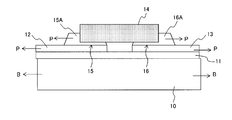
- FIG. 1 shows a mounted state in which chip capacitors are mounted on a metal substrate and connected so as to straddle between wirings.
- a chip capacitor it is often arranged so as to straddle between the power supply wiring and the ground wiring, and the wiring is widened and drawn.
- a metal substrate 10 is made of aluminum, and an insulating coating layer 11 is formed thereon.
- a wiring pattern made of copper foil is formed on the insulating coating layer 11.
- a first wiring 12 (power supply side) and a second wiring 13 (ground side) are formed.
- the first wiring 12 and the second wiring 13 are electrically connected by a chip capacitor 14, and the first wiring 12 and the electrode of the chip capacitor 14 are joined by solder 15 A at the first land portion 15, and the second wiring 13
- the electrode of the chip capacitor 14 is joined to the second land portion 16 by solder 16A.
- a current flows from the first wiring 12 to the chip capacitor 14 via the first land portion 15, and a current flows from the chip capacitor 14 to the second wiring 13 via the second land portion 16.
- This type of configuration is well known and will not be described further.
- the first land portion 15 and the second land portion 16 are respectively formed at the center portion of the end surface E1 of the first wire 12 and the center portion of the end surface E2 of the second wire 13. Is formed.
- the chip capacitor 14 is joined to the first land portion 15 and the second land portion 16 so as to straddle between the first wiring 12 and the second wiring 13.
- Each of the wirings 12 and 13 is a solid wiring made of copper foil.
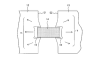
- the metal substrate 10 expands in the direction of arrow B as the temperature rises.
- the wirings 12, 13 and the solder 15A of the land portion 15 mounted thereon and the solder 16A of the land portion 16 are also displaced in the direction of the arrow P.
- the chip capacitor 14 is a ceramic component, the degree of expansion is less than that of the metal substrate 10. Therefore, as shown in FIG. 8, the wirings 12 and 13 generate a stress T (tensile force) that attracts the chip capacitor 14 as a boundary.
- the metal substrate 10 contracts to the side opposite to the direction of arrow B.
- the wirings 12 and 13 and the solder 15A of the land portion 15 mounted thereon and the solder 16A of the land portion 16 are also displaced in the direction opposite to the direction of the arrow P.
- the chip capacitor 14 is a ceramic component, it contracts less than the metal substrate 10. For this reason, the wirings 12 and 13 generate stress (compressive force) that presses against the chip capacitor 14 as a boundary.
- a stress relaxation region having a predetermined number of stress relaxation holes is formed in a wiring region adjacent to a joint portion where the electronic component is joined to the wiring by the conductive bonding agent. is there. According to this, even if stress is generated in the wiring due to heat, the stress acting on the conductive bonding agent is reduced by deformation of the stress relaxation hole, and cracks and the like are suppressed in the conductive bonding agent of the electronic component. Is something that can be done.
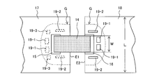
- FIG. 2 is a top view showing the wiring structure according to the first embodiment of the present invention, which is characterized in that a stress relaxation region having a predetermined number of stress relaxation holes is formed around the land portion.
- a wiring pattern made of a copper foil is formed on the insulating coating layer 11 of the metal substrate 10.
- a first wiring 17 (power supply side) and a second wiring 18 (ground side) are formed. Is formed.
- the first wiring 17 and the second wiring 18 are electrically connected by the chip capacitor 14, and the first wiring 17 and the electrode of the chip capacitor 14 are joined by the solder 15 ⁇ / b> A at the first land portion 15, and the second wiring 13.
- the electrode of the chip capacitor 14 is joined to the second land portion 16 by solder 16A.
- the widths of the wirings 17 and 18 are larger than the width W of the chip capacitor 14 and have a width L that is approximately twice or more.
- 15 and the second land portion 16 are formed. Solders 15A and 16A are disposed on these land portions 15 and 16, respectively.
- a predetermined number of stress relaxation holes 19-1 and 19-2 are formed in the stress relaxation region G adjacent to the second land portion 16 of the second wiring 18.
- a total of four elongated stress relaxation holes 19-1 having a rectangular shape and two rectangular stress relaxation holes 19-2 close to a square are formed. It is arranged so as to surround the land portion 16.
- the second land portion 16 is disposed close to (almost flush with) the end surface E2 of the second wiring 18.
- the stress relaxation hole 19-1 is positioned so that at least one stress relaxation hole 19-1 is located within the range of the width W in the stress relaxation region G of the line in which the width W of the chip capacitor 14 is extended. The size of is determined. As a result, the stress acting on the solder 16A of the second land portion 16 at the portion corresponding to the width W of the chip capacitor 14 can be efficiently reduced. In this embodiment, two stress relaxation holes 19-1 are provided.
- the end E2 side of the wiring 18 in the second land portion 16 where the end of the chip capacitor 14 is mounted is thin on the solder 16A, and the end E2 side of the wiring 18
- the corner portion of the solder 16A is likely to be a starting point of cracks.
- elongated stress relaxation holes 19-2 are formed on the side surfaces of the chip capacitor 14, respectively.
- the stress acting on the side surface of the chip capacitor 14 can be reduced, and the amount of cracks generated in the solder 16A can be reduced.
- the stress tends to concentrate on the end face corner of the chip capacitor 14 and the end face corner of the fillet of the solder 16A opposite to the end E2 of the wiring 18.
- the stress relaxation holes 19-2 are arranged in the vicinity of the corners.
- the stress relaxation region G needs to be formed close to the second land portion 16. This is because if the distance from the second land portion 16 is set, the stress generated in the wiring between the second land portion 16 and the stress relaxation region G acts on the solder 16A of the second land portion 16 without being reduced. Therefore, in this embodiment, the distance from the end face of the second land portion 16 to the center of each of the stress relaxation holes 19-1 and 19-2 is set within the stress relaxation region G of the line in which the width W of the chip capacitor 14 is extended. If the width W is smaller than the width W, a sufficient stress relaxation effect can be obtained. In short, it is only necessary that the stress relaxation holes 19-1 and 19-2 are arranged at positions where the stress acting on the solder 16A can be allowed in design.
- the stress relaxation region G is formed in the second wiring 18 on the second land portion 16 side.
- the stress relaxation is applied to the first wiring 17 on the first land portion 15 side.
- the region G can also be formed.
- the position of the stress relaxation hole is different.
- the land portion is located behind the end surface E1 of the first wiring 17 as in the first land portion 15 of FIG. 2, there is a distance between the first land portion 15 and the end surface E1 of the first wiring 17. There is an end surface corner on the end surface E1 side of the first land portion 15 at this portion. For this reason, stress concentrates on this part.
- the stress relaxation hole 19-2 arranged on the side surface side of the chip capacitor 14 is brought close to the end surface E 1 side of the first wiring 17. If the stress relaxation hole 19-2 is lengthened, it can be brought close to the end face corner portion of the first land portion 15. However, if the stress relaxation hole 19-2 is made longer than necessary, the area through which the current of the first wiring 17 flows becomes smaller and the resistance and inductance increase. There's a problem. For this reason, the shape of the stress relaxation hole 19-2 is made close to the end surface corner on the end surface E1 side of the first land portion 15 without changing the shape.
- the stress relaxation hole 19-2 when the stress relaxation hole 19-2 is brought close to the end face corner of the first land portion 15 on the end face E1 side, the end face corner portion of the chip capacitor 14 opposite to the end face E1 side or the solder 15A of the first land portion 15 is provided. Since there is no stress relaxation hole corresponding to the end face corner of the fillet, a new stress relaxation hole 19-3 is formed.
- the stress relaxation holes 19-3 are arranged at positions corresponding to the end face corners of the chip capacitor 14 and the end face corners on the opposite side to the end face E1 side of the fillet of the solder 15A of the first land portion 15.
- the stress relaxation region provided with the predetermined number of stress relaxation holes penetrating the wiring is formed in the vicinity of the joint portion where the chip capacitor is bonded to the wiring by the solder. According to this, even if stress is generated in the wiring due to heat, the stress acting on the conductive bonding agent is reduced by deformation of the stress relaxation hole, and cracks and the like are suppressed in the conductive bonding agent of the electronic component. can do.
- the stress concentration holes 19-1 to 19-3 can be provided with appropriate arcs or chamfers at the time of manufacturing the substrate to reduce the stress concentration, which may cause cracks and the like. Further, the reliability can be improved with respect to the heat cycle of the substrate.
- the second embodiment is the same as the first embodiment in that a predetermined number of stress relaxation holes are formed around the land portion.
- the stress relaxation hole of Example 1 is rectangular, whereas the present example is different in that the whole is a stress relaxation hole formed by an arc, and this is a feature of this example.
- the same reference numerals as those in the first embodiment indicate the same components.
- Example 1 a predetermined number of stress relaxation holes are formed around the land portion, and the shape thereof is rectangular. Therefore, many corners are formed in the wiring by the stress relaxation holes penetrating the wiring. For this reason, a large concentration of current flowing through the wiring occurs, and since the wiring is also a part of the circuit, the inductance is increased and the effect of the original wiring width is reduced. In particular, when a chip capacitor is used, the purpose is to reduce the impedance between wirings, and it is necessary to reduce the effect of increasing the inductance.
- the wiring repeats expansion and contraction corresponding to the expansion and contraction of the metal substrate. For this reason, stress is concentrated at the corners of the rectangular stress relaxation holes, and when a long-term heat cycle is applied, cracks occur from the corners, increasing the resistance due to the decrease in the current passage area. A phenomenon that the wiring is disconnected occurs.
- the stress relaxation hole described below is formed in the wiring in order to solve the above-described problem.
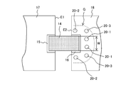
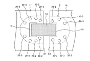
- FIG. 3 is a top view showing a wiring structure according to the second embodiment of the present invention, which is characterized in that a stress relaxation hole having a predetermined number of inner circumferences formed in an arc shape is formed around the land portion. It is.
- a circular stress relaxation hole is proposed as the arc-shaped stress relaxation hole, but a stress relaxation hole such as an ellipse may be used. In short, it is only necessary that the effects of current concentration and stress concentration be improved from the rectangular stress relaxation holes.
- wiring made of copper foil is formed on the insulating coating layer 11 of the metal substrate 10, and here, a first wiring 17 (power supply side) and a second wiring 18 (ground side) are formed. Yes.
- the first wiring 17 and the second wiring 18 are electrically connected by the chip capacitor 14, and the first wiring 17 and the electrode of the chip capacitor 14 are joined by the solder 15 ⁇ / b> A at the first land portion 15, and the second wiring 13.
- the electrode of the chip capacitor 14 is joined to the second land portion 16 by solder 16A.
- a predetermined number of stress relaxation holes 20-1, 20-2, and 20-3 are formed in the stress relaxation region G adjacent to the second land portion 16 of the second wiring 18.
- two circular stress relaxation holes 20-1 provided in the range of the width W in the stress relaxation region G of the line extending the width W of the chip capacitor 14 and the side surfaces of the chip capacitor 14 are provided.
- the two circular stress relaxation holes 20-2 and the two circular stress relaxation holes 20- provided corresponding to the end corners of the chip capacitor 14 and the end corners of the fillets of the solder 16A.
- a total of six are formed, and are arranged so as to surround the second land portion 16 within the range of the stress relaxation region G.
- the first land 15 and the second land portion 16 are disposed close to (almost flush with) the end surface E1 of the first wiring 17 and the end surface E2 of the second wiring 18.
- the shape of the stress relaxation holes 20-1, 20-2, 20-3 is circular, the concentration of current flowing through the wiring is reduced, and an increase in inductance can be suppressed. As a result, when a chip capacitor is used, an increase in inductance is suppressed, so that adverse effects on the chip capacitor 14 can be reduced. Furthermore, since stress can be prevented from concentrating in the stress relaxation holes, the risk of cracking can be reduced even if a long-term heat cycle is applied, and the resistance increases due to the decrease in the current passage area. The phenomenon of disconnection can be avoided.
- At least one stress relaxation hole 20-1 is positioned within the range of the width W in the stress relaxation region G of the line in which the width W of the chip capacitor 14 is extended.
- the size of the stress relaxation hole 20-1 is determined.
- the end E2 side of the wiring 18 in the second land portion 16 where the end of the chip capacitor 14 is mounted is thin on the solder 16A, and the end E2 side of the wiring 18
- the corner portion of the solder 16A is likely to be a starting point of cracks. Therefore, stress relaxation holes 20-2 are formed on the side surfaces of the chip capacitor 14, respectively. As a result, the stress acting on the side surface of the chip capacitor 14 can be reduced, and the amount of cracks generated in the solder 16A can be reduced.
- the stress tends to concentrate on the end face corner of the chip capacitor 14 and the end face corner of the fillet of the solder 16A opposite to the end E2 of the wiring 18.
- the stress relaxation holes 20-3 are arranged near the corners.
- the four stress relaxation holes 20-1 and 20-3 are arranged in a straight line. However, in order to distribute the stress more evenly, the stress relaxation holes 20-3 are arranged at the end face of the fillet of the solder 16A. It is also effective to place it in a circular arc shape closer to the corner. In this case, the distance between the six stress relaxation holes 20-1, 20-2, 20-3 is set to be substantially the same. Thereby, the stress acting on the second land portion 15 can be made substantially uniform.
- the stress relaxation region G needs to be formed close to the second land portion 16. This is because if the distance from the second land portion 16 is set, the stress generated in the wiring between the second land portion 16 and the stress relaxation region G acts on the solder 16A of the second land portion 16 without being reduced. Therefore, in the present embodiment, the distance from the end face of the second land portion 16 to the center of each of the stress relaxation holes 20-1, 20-2, 20-3 is defined as the stress of the line in which the width W of the chip capacitor 14 is extended. When the width is smaller than the width W in the relaxation region G, a sufficient stress relaxation effect can be obtained. In short, it is sufficient that the stress relaxation holes 20-1 to 20-3 are arranged at positions where the stress acting on the solder 16A can be allowed in design.
- the stress relaxation region G is formed in the second wiring 18 on the second land portion 16 side.
- stress is applied to the first wiring 17 on the first land portion 15 side.
- the relaxation region G can be formed.
- the concentration of current flowing through the wiring can be reduced, and the increase in inductance can be suppressed.
- the stress concentration can be suppressed, the occurrence of cracks due to the heat cycle can be reduced, and phenomena such as an increase in resistance due to a decrease in the current passage area and disconnection of the wiring can be avoided.
- the third embodiment is the same as the second embodiment in that a predetermined number of circular stress relaxation holes are formed around the land portion.
- This embodiment is different in that the number of stress relaxation holes is further increased, and this is a feature of this embodiment.
- the same reference numerals as those in the second embodiment denote the same components.
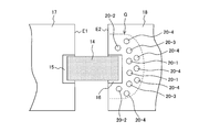
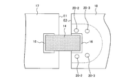
- four stress relaxation holes 20-4 are newly added outside the stress relaxation holes 20-1, 20-2 and 20-3 to form a stress relaxation hole having a double array structure. Moreover, the added stress relaxation hole 20-4 is formed on the side away from the end face E2 of the second wiring 18.
- the stress relaxation hole 20-4 is formed on the side away from the end surface E2 of the second wiring 18, so that the stress generated in the wiring is stress relaxation hole 20-4. Is effectively reduced. Since other operations and effects are the same as those of the second embodiment, a description thereof will be omitted.
- the stress relaxation region G is formed in the second wiring 18 on the second land portion 16 side.
- stress is applied to the first wiring 17 on the first land portion 15 side.
- the relaxation region G can be formed.
- the fourth embodiment is the same as the second embodiment in that a predetermined number of circular stress relaxation holes are formed around the land portion.
- This embodiment is different in that stress relaxation holes are arranged in a portion where stress is concentrated and a portion where cracks are likely to occur. This is a feature of this embodiment.
- the same reference numerals as those in the second and third embodiments indicate the same components.
- the end E2 side of the wiring 18 in the second land portion 16 where the end of the chip capacitor 14 is placed has a thin solder 16A, and the solder 16A on the end E2 side of the wiring 18 is thin. Corners tend to be the starting point for cracks. Therefore, stress relaxation holes 20-2 are formed on the side surfaces of the chip capacitor 14, respectively. As a result, the stress acting on the side surface of the chip capacitor 14 can be reduced, and the amount of cracks generated in the solder 16A can be reduced.
- the stress tends to concentrate on the end face corner of the chip capacitor 14 and the end face corner of the fillet of the solder 16A opposite to the end E2 of the wiring 18.
- the stress relaxation hole 20-3 is provided in the vicinity of the corner portion, and another stress relaxation hole 20-5 is provided in the vicinity thereof. Since the stress relaxation hole 20-3 and the stress relaxation hole 20-5 are formed at positions sandwiching the end face corner of the chip capacitor 14 and the end face corner of the fillet of the solder 16A, the end face corner of the chip capacitor 14 and the solder The stress concentrated on the end face corner of the 16A fillet can be effectively reduced.
- the stress relaxation holes are provided only in the portion where stress is concentrated and the portion where cracks are likely to occur, the strength of the wiring is not so much impaired.
- the stress relaxation holes are not provided more than necessary, a sufficient current passage area can be obtained and increase in inductance and electrical resistance can be suppressed. Since other operations and effects are the same as those of the second embodiment, a description thereof will be omitted.
- the stress relaxation region G is formed in the second wiring 18 on the second land portion 16 side.
- stress is applied to the first wiring 17 on the first land portion 15 side.
- the relaxation region G can be formed.
- the arrangement position of the stress relaxation holes is different.
- the land portion is located behind the end surface E1 of the first wiring 17 as in the first land portion 15
- the corner of the end face of the first land portion 15 is located in the portion. For this reason, stress concentrates on this part.
- one stress relaxation hole 20-2 which has been arranged on the side surface side of the chip capacitor 14, is added and provided close to the end surface E1 side of the first wiring 17.
- the two stress relaxation holes 20-2 are arranged so as to sandwich the end face corner portion of the first land portion 15 on the end face E1 side of the first wiring 17.
- the fifth embodiment is the same as the second embodiment in that a predetermined number of circular stress relaxation holes are formed around the land portion.
- the difference is that a minimum stress relaxation hole is disposed in a portion where stress is concentrated and a portion where cracks are likely to occur, and two stress relaxation holes are reduced compared to the fourth embodiment.
- the same reference numerals as those in the fourth embodiment denote the same components.
- the end E2 side of the wiring 18 in the second land portion 16 where the end of the chip capacitor 14 is placed has a thin solder 16A, and the solder 16A on the end E2 side of the wiring 18 is thin. Corners tend to be the starting point for cracks. For this reason, 20-2 are formed on the side surfaces of the chip capacitor 14, respectively. As a result, the stress acting on the side surface of the chip capacitor 14 can be reduced, and the amount of cracks generated in the solder 16A can be reduced.
- stress relaxation holes 20-3 are provided in the vicinity of the corners. Since the stress relaxation hole 20-3 is formed close to the end face corner of the chip capacitor 14 and the end face corner of the solder 16A, the end face corner of the chip capacitor 14 and the end face corner of the fillet of the solder 16A. It is possible to effectively reduce the stress concentrated on the.
- the stress relaxation holes are provided only in the portion where the stress is concentrated and the portion where the crack is likely to occur, the strength of the wiring is not so much deteriorated. Further, since the stress relaxation holes are not provided more than necessary, a sufficient current passage area can be secured to prevent an increase in electrical resistance. Since other operations and effects are the same as those of the second embodiment, a description thereof will be omitted.
- the stress relaxation region G is formed in the second wiring 18 on the second land portion 16 side.
- stress is applied to the first wiring 17 on the first land portion 15 side.
- the relaxation region G can be formed.
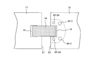
- the chip capacitor 14 is formed on the side surface side with respect to the area of the stress relaxation hole 20-3 formed in the vicinity of the end surface corner of the chip capacitor 14 and the end surface corner of the fillet of the solder 16A. 6 is different from the embodiment of FIG. 6 in that the area of the stress relaxation hole 20-2A is reduced.
- stress relaxation holes 20-2A having a diameter smaller than the stress relaxation holes 20-3 are formed on the side surfaces of the chip capacitor 14, respectively.
- the stress acting on the side surface of the chip capacitor 14 is reduced, and the risk of cracks occurring in the thin solder 16A is reduced.
- the reason why the diameter of the stress relaxation hole 20-2A is reduced is as follows.
- the purpose of the circuit element of the chip capacitor 14 is to reduce the impedance between the wiring 17 and the wiring 18, but the main current flowing through the wiring 18 flows along the central axis in the width direction of the chip capacitor 14.
- the side surface of the chip capacitor 14 is such that the area ratio between the wiring area and the stress relaxation hole is relatively close to the central axis side. As a result, the stress relaxation hole smaller than the stress relaxation hole 20-3. 20-2A is arranged.
- the diameter of the stress relaxation hole 20-2A is reduced according to the wiring width on the side located on the side surface of the chip capacitor 14, the effect of reducing the stress is ensured, and the diameter is reduced according to the wiring width. Therefore, the occupation ratio in the wiring of the stress relaxation hole 20-2A occupying between the side surface side of the chip capacitor 14 and the side end surface of the second wiring 18 is reduced, and a sufficient current passage area can be maintained. it can.
- the stress relaxation hole 20-3 on the side in the longitudinal direction of the chip capacitor 14 is increased in diameter to increase the stress reduction rate, and even if the diameter is increased, the stress relaxation hole 20- in the longitudinal direction of the wiring is increased. Since the occupation ratio in the wiring of 2A does not become so large, a sufficient current passage area can be maintained.
- the chip capacitor is exemplified as the electronic component to be mounted on the surface.
- a chip resistor or an FET which is a semiconductor element may be mounted in addition to this.
- a configuration is provided in which a stress relaxation region is formed in which a predetermined number of stress relaxation holes that penetrate the wiring are provided in the vicinity of the joint portion where the electronic component is bonded to the wiring by the conductive bonding agent. did.
- the stress acting on the conductive bonding agent is reduced by deformation of the stress relaxation hole, and the occurrence of cracks or the like in the conductive bonding agent of the electronic component is suppressed. Can do.
- this invention is not limited to the above-mentioned Example, Various modifications are included.
- the above-described embodiments have been described in detail for easy understanding of the present invention, and are not necessarily limited to those having all the configurations described.
- a part of the configuration of one embodiment can be replaced with the configuration of another embodiment, and the configuration of another embodiment can be added to the configuration of one embodiment.
Landscapes
- Engineering & Computer Science (AREA)
- Microelectronics & Electronic Packaging (AREA)
- Structures For Mounting Electric Components On Printed Circuit Boards (AREA)
- Structure Of Printed Boards (AREA)
- Insulated Metal Substrates For Printed Circuits (AREA)
- Wire Bonding (AREA)
- Electric Connection Of Electric Components To Printed Circuits (AREA)
- Connections Effected By Soldering, Adhesion, Or Permanent Deformation (AREA)
Abstract
Description
このため、本実施例では、第2ランド部16の端面から各応力緩和孔19-1、19-2の中心までの距離を、チップコンデンサ14の幅Wを延長した線の応力緩和領域G内の幅Wより小さくすると充分な応力緩和効果を得ることができる。要は、ハンダ16Aに作用する応力を設計的に許容できる位置に応力緩和孔19-1、19-2が配置されていれば良いものである。
ただ、ランド部を形成する位置が第2ランド部16のような位置にない場合は応力緩和孔の配置位置が異なってくる。図2の第1ランド部15のように、第1配線17の端面E1より奥側にランド部が位置する場合では、第1ランド部15と第1配線17の端面E1との間に距離があり、この部分に第1ランド部15の端面E1側の端面角部が位置することになる。このため、この部分に応力が集中することになる。
これによれば、熱によって配線に応力が発生しても、応力緩和孔が変形することによって導電接合剤に作用する応力が小さくなり、電子部品の導電接合剤にクラック等が発生するのを抑制することができる。
Claims (11)
- 少なくとも、金属基板と、前記金属基板上に形成された配線と、前記配線の一部と導電性接合剤によって接合された電子部品とを備えた電子制御装置において、
前記電子部品を前記配線に接合する接合部分に近接した配線部分に、前記配線を貫通する所定数の応力緩和孔を設けた応力緩和領域を形成したことを特徴とする電子制御装置。 - 請求項1に記載の電子制御装置において、
前記配線の幅は前記電子部品の接合される幅の2倍以上であり、前記配線の端面上に前記導電性接合剤が配置されるランド部が形成されており、更に前記ランド部の周囲に前記所定数の応力緩和孔が配置されていることを特徴とする電子制御装置。 - 請求項2に記載の電子制御装置において、
前記応力緩和孔は、少なくとも、前記電子部品の側面付近と、前記電子部品の角部付近、或いは前記導電性接合剤のフィレットの角部付近に、少なくとも1個以上設けられていることを特徴とする電子制御装置。 - 請求項3に記載の電子制御装置において、
前記応力緩和孔は、更に前記電子部品の接合される幅を延長した線の前記応力緩和領域G内の前記幅の範囲内に、少なくとも1個以上設けられていることを特徴とする電子制御装置。 - 請求項1乃至請求項4のいずれかに記載の電子制御装置において、
前記応力緩和孔の形状は矩形である、或いは円弧状であることを特徴とする電子制御装置。 - 請求項5に記載の電子制御装置において、
前記円弧状の応力緩和孔は、円形の応力緩和孔であることを特徴とする電子制御装置。 - 請求項2に記載の電子制御装置において、
前記応力緩和孔の中心と前記ランド部の端面との間の距離は、前記電子部品の幅を延長した線の前記応力緩和領域G内の幅より小さいことを特徴とする電子制御装置。 - 少なくとも、金属基板と、前記金属基板上に形成された配線と、前記配線の一部と導電性接合剤によって接合されたチップコンデンサとを備えた電子制御装置において、
前記配線の幅は前記電子部品の接合される幅の2倍以上であり、前記配線の端面上に前記導電性接合剤が配置されるランド部が形成されており、前記更に前記ランド部の周囲に所定数の円形の応力緩和孔が配置されていることを特徴とする電子制御装置。 - 請求項8に記載の電子制御装置において、
前記チップコンデンサが接続される前記配線は電源配線とグランド配線であり、前記両配線の一方、或いは両方の前記ランド部の周囲に所定数の応力緩和孔が配置されていることを特徴とする電子制御装置。 - 請求項9に記載の電子制御装置において、
前記応力緩和孔は、少なくとも、前記電子部品の側面付近と、前記電子部品の角部付近、或いは前記導電性接合剤のフィレットの角部付近に、少なくとも1個以上設けられていることを特徴とする電子制御装置。 - 請求項10に記載の電子制御装置において、
前記電子部品の角部付近、或いは前記導電性接合剤のフィレットの角部付近の応力緩和孔が、前記電子部品の側面付近の応力緩和孔の面積より大きいことを特徴とする電子制御装置。
Priority Applications (4)
| Application Number | Priority Date | Filing Date | Title |
|---|---|---|---|
| KR1020177015466A KR102076893B1 (ko) | 2015-01-13 | 2015-09-09 | 전자 제어 장치 |
| CN201580069266.4A CN107113962B (zh) | 2015-01-13 | 2015-09-09 | 电子控制装置 |
| DE112015005933.4T DE112015005933T5 (de) | 2015-01-13 | 2015-09-09 | Elektronische Steuervorrichtung |
| US15/542,916 US10251271B2 (en) | 2015-01-13 | 2015-09-09 | Electronic control device |
Applications Claiming Priority (2)
| Application Number | Priority Date | Filing Date | Title |
|---|---|---|---|
| JP2015003764A JP6497942B2 (ja) | 2015-01-13 | 2015-01-13 | 電子制御装置 |
| JP2015-003764 | 2015-01-13 |
Publications (1)
| Publication Number | Publication Date |
|---|---|
| WO2016113945A1 true WO2016113945A1 (ja) | 2016-07-21 |
Family
ID=56405503
Family Applications (1)
| Application Number | Title | Priority Date | Filing Date |
|---|---|---|---|
| PCT/JP2015/075538 Ceased WO2016113945A1 (ja) | 2015-01-13 | 2015-09-09 | 電子制御装置 |
Country Status (6)
| Country | Link |
|---|---|
| US (1) | US10251271B2 (ja) |
| JP (1) | JP6497942B2 (ja) |
| KR (1) | KR102076893B1 (ja) |
| CN (1) | CN107113962B (ja) |
| DE (1) | DE112015005933T5 (ja) |
| WO (1) | WO2016113945A1 (ja) |
Families Citing this family (6)
| Publication number | Priority date | Publication date | Assignee | Title |
|---|---|---|---|---|
| KR102837100B1 (ko) * | 2020-01-14 | 2025-07-22 | 주식회사 엘지에너지솔루션 | Bmu 부품 손상 방지 구조를 포함하는 배터리 팩 |
| CN112616244B (zh) * | 2020-12-22 | 2022-03-22 | 浙江清华柔性电子技术研究院 | 柔性电路板及柔性电路板制备方法 |
| JP7703855B2 (ja) * | 2021-01-14 | 2025-07-08 | 住友電気工業株式会社 | 半導体装置 |
| KR102914808B1 (ko) * | 2021-02-09 | 2026-01-19 | 현대모비스 주식회사 | 회로기판 조립체 |
| WO2025173452A1 (ja) * | 2024-02-16 | 2025-08-21 | 三菱電機株式会社 | プリント回路装置及び電力変換装置 |
| DE102025101846A1 (de) * | 2025-01-20 | 2026-07-23 | HELLA GmbH & Co. KGaA | Substratträger und Kraftfahrzeug |
Citations (2)
| Publication number | Priority date | Publication date | Assignee | Title |
|---|---|---|---|---|
| JP2008072065A (ja) * | 2006-09-15 | 2008-03-27 | Toyota Industries Corp | 表面実装用電子部品の表面実装構造 |
| JP2011151368A (ja) * | 2009-12-24 | 2011-08-04 | Furukawa Electric Co Ltd:The | 射出成形基板と実装部品との取付構造 |
Family Cites Families (20)
| Publication number | Priority date | Publication date | Assignee | Title |
|---|---|---|---|---|
| JPS6052660U (ja) * | 1983-09-14 | 1985-04-13 | アルプス電気株式会社 | プリント基板 |
| US4641222A (en) * | 1984-05-29 | 1987-02-03 | Motorola, Inc. | Mounting system for stress relief in surface mounted components |
| JPS62217695A (ja) * | 1986-03-19 | 1987-09-25 | 古河電気工業株式会社 | プリント回路板 |
| US4777564A (en) * | 1986-10-16 | 1988-10-11 | Motorola, Inc. | Leadform for use with surface mounted components |
| JPS63241979A (ja) * | 1987-03-30 | 1988-10-07 | 沖電気工業株式会社 | 印刷配線板 |
| JPH01289186A (ja) * | 1988-05-16 | 1989-11-21 | Toyo Commun Equip Co Ltd | プリント基板 |
| JP2844085B2 (ja) * | 1989-07-20 | 1999-01-06 | セイコーインスツルメンツ株式会社 | 回路基板及び半導体素子の実装方法 |
| JPH04159792A (ja) * | 1990-10-23 | 1992-06-02 | Tamura Seisakusho Co Ltd | 金属コア基板 |
| JPH04338599A (ja) * | 1991-05-15 | 1992-11-25 | Hitachi Ltd | 実装基板およびその実装構造 |
| JP2553102Y2 (ja) * | 1991-08-23 | 1997-11-05 | 日本電気株式会社 | チップ部品搭載配線基板 |
| JPH07142821A (ja) * | 1993-11-15 | 1995-06-02 | Matsushita Electric Ind Co Ltd | プリント配線板 |
| JPH098444A (ja) * | 1995-04-20 | 1997-01-10 | Sony Corp | 電子回路装置 |
| JPH11154781A (ja) * | 1997-11-20 | 1999-06-08 | Matsushita Electric Ind Co Ltd | リードレス部品を搭載した回路モジュール |
| JP3456145B2 (ja) * | 1998-05-27 | 2003-10-14 | 松下電器産業株式会社 | 実装基板 |
| JP2007180240A (ja) * | 2005-12-27 | 2007-07-12 | Sharp Corp | 多層配線基板と、それを備えた電子モジュールおよび電子機器 |
| JP2007250815A (ja) * | 2006-03-16 | 2007-09-27 | Fujikura Ltd | フレキシブルプリント基板及びそれを用いた電子部品実装回路 |
| CN102668726B (zh) | 2009-12-24 | 2015-07-01 | 古河电气工业株式会社 | 注塑成型基板与实装零件的安装结构 |
| US9082707B2 (en) * | 2010-11-25 | 2015-07-14 | Mitsubshi Electric Corporation | Semiconductor device and method for manufacturing semiconductor device |
| JP2013197138A (ja) * | 2012-03-16 | 2013-09-30 | Panasonic Corp | プリント基板 |
| JP2013239470A (ja) * | 2012-05-11 | 2013-11-28 | Fuji Electric Fa Components & Systems Co Ltd | 表面実装基板 |
-
2015
- 2015-01-13 JP JP2015003764A patent/JP6497942B2/ja active Active
- 2015-09-09 KR KR1020177015466A patent/KR102076893B1/ko not_active Expired - Fee Related
- 2015-09-09 US US15/542,916 patent/US10251271B2/en active Active
- 2015-09-09 WO PCT/JP2015/075538 patent/WO2016113945A1/ja not_active Ceased
- 2015-09-09 DE DE112015005933.4T patent/DE112015005933T5/de active Pending
- 2015-09-09 CN CN201580069266.4A patent/CN107113962B/zh active Active
Patent Citations (2)
| Publication number | Priority date | Publication date | Assignee | Title |
|---|---|---|---|---|
| JP2008072065A (ja) * | 2006-09-15 | 2008-03-27 | Toyota Industries Corp | 表面実装用電子部品の表面実装構造 |
| JP2011151368A (ja) * | 2009-12-24 | 2011-08-04 | Furukawa Electric Co Ltd:The | 射出成形基板と実装部品との取付構造 |
Also Published As
| Publication number | Publication date |
|---|---|
| JP6497942B2 (ja) | 2019-04-10 |
| CN107113962A (zh) | 2017-08-29 |
| US10251271B2 (en) | 2019-04-02 |
| JP2016131164A (ja) | 2016-07-21 |
| DE112015005933T5 (de) | 2017-10-19 |
| KR102076893B1 (ko) | 2020-05-18 |
| US20180007787A1 (en) | 2018-01-04 |
| CN107113962B (zh) | 2019-06-07 |
| KR20170081242A (ko) | 2017-07-11 |
Similar Documents
| Publication | Publication Date | Title |
|---|---|---|
| JP6497942B2 (ja) | 電子制御装置 | |
| KR101529900B1 (ko) | 전자부품 | |
| JP5459444B2 (ja) | 電子部品 | |
| JP5459445B2 (ja) | 電子部品 | |
| JP5465281B2 (ja) | チップ部品の実装構造 | |
| JP2016213308A (ja) | プリント回路板及びプリント配線板 | |
| JP7124795B2 (ja) | 電子部品モジュール、電子部品ユニット、および、電子部品モジュールの製造方法 | |
| CN105144855B (zh) | 电子控制装置 | |
| JP5459368B2 (ja) | チップ部品構造体 | |
| WO2020235583A1 (ja) | 抵抗器 | |
| JP6289063B2 (ja) | 電子部品実装装置及びそれを備える半導体装置 | |
| WO2016031440A1 (ja) | チップ抵抗器およびその実装構造 | |
| JP2018200918A (ja) | パワーモジュール | |
| JP6565167B2 (ja) | 実装構造体 | |
| JP2016015449A (ja) | チップ抵抗器 | |
| JPWO2015151810A1 (ja) | チップ型電子部品 | |
| JP2006294932A (ja) | 回路実装基板のランドおよび表面実装部品が搭載された回路実装基板 | |
| JP2018113316A (ja) | 複合電子部品 | |
| JP6004579B2 (ja) | 半導体装置 | |
| JP2023161397A (ja) | 回路基板 | |
| JPH0951059A (ja) | チップ状電子部品 | |
| JP2007150201A (ja) | チップ抵抗器 | |
| JP2007116039A (ja) | 回路基板 | |
| JP2020072096A (ja) | 実装基板 | |
| JP2008311345A (ja) | チップ電子部品及びチップ電子部品の実装構造 |
Legal Events
| Date | Code | Title | Description |
|---|---|---|---|
| 121 | Ep: the epo has been informed by wipo that ep was designated in this application |
Ref document number: 15877897 Country of ref document: EP Kind code of ref document: A1 |
|
| ENP | Entry into the national phase |
Ref document number: 20177015466 Country of ref document: KR Kind code of ref document: A |
|
| WWE | Wipo information: entry into national phase |
Ref document number: 15542916 Country of ref document: US |
|
| WWE | Wipo information: entry into national phase |
Ref document number: 112015005933 Country of ref document: DE |
|
| 122 | Ep: pct application non-entry in european phase |
Ref document number: 15877897 Country of ref document: EP Kind code of ref document: A1 |