WO2015186560A1 - ムライト焼結体、その製法及び複合基板 - Google Patents
ムライト焼結体、その製法及び複合基板 Download PDFInfo
- Publication number
- WO2015186560A1 WO2015186560A1 PCT/JP2015/065006 JP2015065006W WO2015186560A1 WO 2015186560 A1 WO2015186560 A1 WO 2015186560A1 JP 2015065006 W JP2015065006 W JP 2015065006W WO 2015186560 A1 WO2015186560 A1 WO 2015186560A1
- Authority
- WO
- WIPO (PCT)
- Prior art keywords
- mullite
- sintered body
- substrate
- mullite sintered
- less
- Prior art date
- Legal status (The legal status is an assumption and is not a legal conclusion. Google has not performed a legal analysis and makes no representation as to the accuracy of the status listed.)
- Ceased
Links
Images


Classifications
-
- C—CHEMISTRY; METALLURGY
- C04—CEMENTS; CONCRETE; ARTIFICIAL STONE; CERAMICS; REFRACTORIES
- C04B—LIME, MAGNESIA; SLAG; CEMENTS; COMPOSITIONS THEREOF, e.g. MORTARS, CONCRETE OR LIKE BUILDING MATERIALS; ARTIFICIAL STONE; CERAMICS; REFRACTORIES; TREATMENT OF NATURAL STONE
- C04B35/00—Shaped ceramic products characterised by their composition; Ceramics compositions; Processing powders of inorganic compounds preparatory to the manufacturing of ceramic products
- C04B35/01—Shaped ceramic products characterised by their composition; Ceramics compositions; Processing powders of inorganic compounds preparatory to the manufacturing of ceramic products based on oxide ceramics
- C04B35/16—Shaped ceramic products characterised by their composition; Ceramics compositions; Processing powders of inorganic compounds preparatory to the manufacturing of ceramic products based on oxide ceramics based on silicates other than clay
- C04B35/18—Shaped ceramic products characterised by their composition; Ceramics compositions; Processing powders of inorganic compounds preparatory to the manufacturing of ceramic products based on oxide ceramics based on silicates other than clay rich in aluminium oxide
- C04B35/185—Mullite 3Al2O3-2SiO2
-
- C—CHEMISTRY; METALLURGY
- C04—CEMENTS; CONCRETE; ARTIFICIAL STONE; CERAMICS; REFRACTORIES
- C04B—LIME, MAGNESIA; SLAG; CEMENTS; COMPOSITIONS THEREOF, e.g. MORTARS, CONCRETE OR LIKE BUILDING MATERIALS; ARTIFICIAL STONE; CERAMICS; REFRACTORIES; TREATMENT OF NATURAL STONE
- C04B35/00—Shaped ceramic products characterised by their composition; Ceramics compositions; Processing powders of inorganic compounds preparatory to the manufacturing of ceramic products
- C04B35/622—Forming processes; Processing powders of inorganic compounds preparatory to the manufacturing of ceramic products
- C04B35/64—Burning or sintering processes
- C04B35/645—Pressure sintering
-
- C—CHEMISTRY; METALLURGY
- C04—CEMENTS; CONCRETE; ARTIFICIAL STONE; CERAMICS; REFRACTORIES
- C04B—LIME, MAGNESIA; SLAG; CEMENTS; COMPOSITIONS THEREOF, e.g. MORTARS, CONCRETE OR LIKE BUILDING MATERIALS; ARTIFICIAL STONE; CERAMICS; REFRACTORIES; TREATMENT OF NATURAL STONE
- C04B37/00—Joining burned ceramic articles with other burned ceramic articles or other articles by heating
- C04B37/001—Joining burned ceramic articles with other burned ceramic articles or other articles by heating directly with other burned ceramic articles
-
- C—CHEMISTRY; METALLURGY
- C04—CEMENTS; CONCRETE; ARTIFICIAL STONE; CERAMICS; REFRACTORIES
- C04B—LIME, MAGNESIA; SLAG; CEMENTS; COMPOSITIONS THEREOF, e.g. MORTARS, CONCRETE OR LIKE BUILDING MATERIALS; ARTIFICIAL STONE; CERAMICS; REFRACTORIES; TREATMENT OF NATURAL STONE
- C04B37/00—Joining burned ceramic articles with other burned ceramic articles or other articles by heating
- C04B37/008—Joining burned ceramic articles with other burned ceramic articles or other articles by heating by means of an interlayer consisting of an organic adhesive, e.g. phenol resin or pitch
-
- C—CHEMISTRY; METALLURGY
- C04—CEMENTS; CONCRETE; ARTIFICIAL STONE; CERAMICS; REFRACTORIES
- C04B—LIME, MAGNESIA; SLAG; CEMENTS; COMPOSITIONS THEREOF, e.g. MORTARS, CONCRETE OR LIKE BUILDING MATERIALS; ARTIFICIAL STONE; CERAMICS; REFRACTORIES; TREATMENT OF NATURAL STONE
- C04B37/00—Joining burned ceramic articles with other burned ceramic articles or other articles by heating
- C04B37/02—Joining burned ceramic articles with other burned ceramic articles or other articles by heating with metallic articles
-
- C—CHEMISTRY; METALLURGY
- C04—CEMENTS; CONCRETE; ARTIFICIAL STONE; CERAMICS; REFRACTORIES
- C04B—LIME, MAGNESIA; SLAG; CEMENTS; COMPOSITIONS THEREOF, e.g. MORTARS, CONCRETE OR LIKE BUILDING MATERIALS; ARTIFICIAL STONE; CERAMICS; REFRACTORIES; TREATMENT OF NATURAL STONE
- C04B2235/00—Aspects relating to ceramic starting mixtures or sintered ceramic products
- C04B2235/02—Composition of constituents of the starting material or of secondary phases of the final product
- C04B2235/50—Constituents or additives of the starting mixture chosen for their shape or used because of their shape or their physical appearance
- C04B2235/54—Particle size related information
- C04B2235/5418—Particle size related information expressed by the size of the particles or aggregates thereof
- C04B2235/5436—Particle size related information expressed by the size of the particles or aggregates thereof micrometer sized, i.e. from 1 to 100 micron
-
- C—CHEMISTRY; METALLURGY
- C04—CEMENTS; CONCRETE; ARTIFICIAL STONE; CERAMICS; REFRACTORIES
- C04B—LIME, MAGNESIA; SLAG; CEMENTS; COMPOSITIONS THEREOF, e.g. MORTARS, CONCRETE OR LIKE BUILDING MATERIALS; ARTIFICIAL STONE; CERAMICS; REFRACTORIES; TREATMENT OF NATURAL STONE
- C04B2235/00—Aspects relating to ceramic starting mixtures or sintered ceramic products
- C04B2235/02—Composition of constituents of the starting material or of secondary phases of the final product
- C04B2235/50—Constituents or additives of the starting mixture chosen for their shape or used because of their shape or their physical appearance
- C04B2235/54—Particle size related information
- C04B2235/5418—Particle size related information expressed by the size of the particles or aggregates thereof
- C04B2235/5445—Particle size related information expressed by the size of the particles or aggregates thereof submicron sized, i.e. from 0,1 to 1 micron
-
- C—CHEMISTRY; METALLURGY
- C04—CEMENTS; CONCRETE; ARTIFICIAL STONE; CERAMICS; REFRACTORIES
- C04B—LIME, MAGNESIA; SLAG; CEMENTS; COMPOSITIONS THEREOF, e.g. MORTARS, CONCRETE OR LIKE BUILDING MATERIALS; ARTIFICIAL STONE; CERAMICS; REFRACTORIES; TREATMENT OF NATURAL STONE
- C04B2235/00—Aspects relating to ceramic starting mixtures or sintered ceramic products
- C04B2235/65—Aspects relating to heat treatments of ceramic bodies such as green ceramics or pre-sintered ceramics, e.g. burning, sintering or melting processes
- C04B2235/656—Aspects relating to heat treatments of ceramic bodies such as green ceramics or pre-sintered ceramics, e.g. burning, sintering or melting processes characterised by specific heating conditions during heat treatment
- C04B2235/6562—Heating rate
-
- C—CHEMISTRY; METALLURGY
- C04—CEMENTS; CONCRETE; ARTIFICIAL STONE; CERAMICS; REFRACTORIES
- C04B—LIME, MAGNESIA; SLAG; CEMENTS; COMPOSITIONS THEREOF, e.g. MORTARS, CONCRETE OR LIKE BUILDING MATERIALS; ARTIFICIAL STONE; CERAMICS; REFRACTORIES; TREATMENT OF NATURAL STONE
- C04B2235/00—Aspects relating to ceramic starting mixtures or sintered ceramic products
- C04B2235/65—Aspects relating to heat treatments of ceramic bodies such as green ceramics or pre-sintered ceramics, e.g. burning, sintering or melting processes
- C04B2235/656—Aspects relating to heat treatments of ceramic bodies such as green ceramics or pre-sintered ceramics, e.g. burning, sintering or melting processes characterised by specific heating conditions during heat treatment
- C04B2235/6565—Cooling rate
-
- C—CHEMISTRY; METALLURGY
- C04—CEMENTS; CONCRETE; ARTIFICIAL STONE; CERAMICS; REFRACTORIES
- C04B—LIME, MAGNESIA; SLAG; CEMENTS; COMPOSITIONS THEREOF, e.g. MORTARS, CONCRETE OR LIKE BUILDING MATERIALS; ARTIFICIAL STONE; CERAMICS; REFRACTORIES; TREATMENT OF NATURAL STONE
- C04B2235/00—Aspects relating to ceramic starting mixtures or sintered ceramic products
- C04B2235/65—Aspects relating to heat treatments of ceramic bodies such as green ceramics or pre-sintered ceramics, e.g. burning, sintering or melting processes
- C04B2235/658—Atmosphere during thermal treatment
- C04B2235/6586—Processes characterised by the flow of gas
-
- C—CHEMISTRY; METALLURGY
- C04—CEMENTS; CONCRETE; ARTIFICIAL STONE; CERAMICS; REFRACTORIES
- C04B—LIME, MAGNESIA; SLAG; CEMENTS; COMPOSITIONS THEREOF, e.g. MORTARS, CONCRETE OR LIKE BUILDING MATERIALS; ARTIFICIAL STONE; CERAMICS; REFRACTORIES; TREATMENT OF NATURAL STONE
- C04B2235/00—Aspects relating to ceramic starting mixtures or sintered ceramic products
- C04B2235/70—Aspects relating to sintered or melt-casted ceramic products
- C04B2235/74—Physical characteristics
- C04B2235/77—Density
-
- C—CHEMISTRY; METALLURGY
- C04—CEMENTS; CONCRETE; ARTIFICIAL STONE; CERAMICS; REFRACTORIES
- C04B—LIME, MAGNESIA; SLAG; CEMENTS; COMPOSITIONS THEREOF, e.g. MORTARS, CONCRETE OR LIKE BUILDING MATERIALS; ARTIFICIAL STONE; CERAMICS; REFRACTORIES; TREATMENT OF NATURAL STONE
- C04B2235/00—Aspects relating to ceramic starting mixtures or sintered ceramic products
- C04B2235/70—Aspects relating to sintered or melt-casted ceramic products
- C04B2235/74—Physical characteristics
- C04B2235/78—Grain sizes and shapes, product microstructures, e.g. acicular grains, equiaxed grains, platelet-structures
- C04B2235/785—Submicron sized grains, i.e. from 0,1 to 1 micron
-
- C—CHEMISTRY; METALLURGY
- C04—CEMENTS; CONCRETE; ARTIFICIAL STONE; CERAMICS; REFRACTORIES
- C04B—LIME, MAGNESIA; SLAG; CEMENTS; COMPOSITIONS THEREOF, e.g. MORTARS, CONCRETE OR LIKE BUILDING MATERIALS; ARTIFICIAL STONE; CERAMICS; REFRACTORIES; TREATMENT OF NATURAL STONE
- C04B2235/00—Aspects relating to ceramic starting mixtures or sintered ceramic products
- C04B2235/70—Aspects relating to sintered or melt-casted ceramic products
- C04B2235/96—Properties of ceramic products, e.g. mechanical properties such as strength, toughness, wear resistance
- C04B2235/963—Surface properties, e.g. surface roughness
-
- C—CHEMISTRY; METALLURGY
- C04—CEMENTS; CONCRETE; ARTIFICIAL STONE; CERAMICS; REFRACTORIES
- C04B—LIME, MAGNESIA; SLAG; CEMENTS; COMPOSITIONS THEREOF, e.g. MORTARS, CONCRETE OR LIKE BUILDING MATERIALS; ARTIFICIAL STONE; CERAMICS; REFRACTORIES; TREATMENT OF NATURAL STONE
- C04B2235/00—Aspects relating to ceramic starting mixtures or sintered ceramic products
- C04B2235/70—Aspects relating to sintered or melt-casted ceramic products
- C04B2235/96—Properties of ceramic products, e.g. mechanical properties such as strength, toughness, wear resistance
- C04B2235/9646—Optical properties
- C04B2235/9653—Translucent or transparent ceramics other than alumina
-
- C—CHEMISTRY; METALLURGY
- C04—CEMENTS; CONCRETE; ARTIFICIAL STONE; CERAMICS; REFRACTORIES
- C04B—LIME, MAGNESIA; SLAG; CEMENTS; COMPOSITIONS THEREOF, e.g. MORTARS, CONCRETE OR LIKE BUILDING MATERIALS; ARTIFICIAL STONE; CERAMICS; REFRACTORIES; TREATMENT OF NATURAL STONE
- C04B2237/00—Aspects relating to ceramic laminates or to joining of ceramic articles with other articles by heating
- C04B2237/30—Composition of layers of ceramic laminates or of ceramic or metallic articles to be joined by heating, e.g. Si substrates
- C04B2237/32—Ceramic
- C04B2237/34—Oxidic
-
- C—CHEMISTRY; METALLURGY
- C04—CEMENTS; CONCRETE; ARTIFICIAL STONE; CERAMICS; REFRACTORIES
- C04B—LIME, MAGNESIA; SLAG; CEMENTS; COMPOSITIONS THEREOF, e.g. MORTARS, CONCRETE OR LIKE BUILDING MATERIALS; ARTIFICIAL STONE; CERAMICS; REFRACTORIES; TREATMENT OF NATURAL STONE
- C04B2237/00—Aspects relating to ceramic laminates or to joining of ceramic articles with other articles by heating
- C04B2237/50—Processing aspects relating to ceramic laminates or to the joining of ceramic articles with other articles by heating
- C04B2237/55—Pre-treatments of a coated or not coated substrate other than oxidation treatment in order to form an active joining layer
-
- C—CHEMISTRY; METALLURGY
- C04—CEMENTS; CONCRETE; ARTIFICIAL STONE; CERAMICS; REFRACTORIES
- C04B—LIME, MAGNESIA; SLAG; CEMENTS; COMPOSITIONS THEREOF, e.g. MORTARS, CONCRETE OR LIKE BUILDING MATERIALS; ARTIFICIAL STONE; CERAMICS; REFRACTORIES; TREATMENT OF NATURAL STONE
- C04B2237/00—Aspects relating to ceramic laminates or to joining of ceramic articles with other articles by heating
- C04B2237/50—Processing aspects relating to ceramic laminates or to the joining of ceramic articles with other articles by heating
- C04B2237/72—Forming laminates or joined articles comprising at least two interlayers directly next to each other
Definitions
- the present invention relates to a mullite sintered body, a manufacturing method thereof, and a composite substrate.
- the mullite sintered body is generally a material having excellent thermal shock resistance obtained by sintering aluminum oxide (Al 2 O 3 ) and silicon oxide (SiO 2 ) in a ratio of 3 to 2, and 3Al 2 O 3 .2SiO 2. It is represented by As such a mullite sintered body, for example, as disclosed in Patent Document 1, a powder obtained by mixing 30% by mass of yttria-stabilized zirconia (YSZ) powder with mullite powder was molded, and the molded body was sintered. Things are known. In Patent Document 1, a mullite substrate is cut out from a mullite sintered body, and the main surface of the mullite substrate is polished to be a base substrate used for bonding to a GaN substrate.
- YSZ yttria-stabilized zirconia
- the thermal expansion coefficient of GaN is 6.0 ppm / K in the range from room temperature to 1000 ° C., and the thermal expansion coefficient of mullite is 5.2 ppm / K. Therefore, in consideration of using the two together, it is preferable to increase the coefficient of thermal expansion of mullite to approach the coefficient of thermal expansion of the GaN substrate. Therefore, mullite powder is mixed with YSZ powder and sintered. .
- Patent Document 1 a mullite sintered body in which a thermal expansion coefficient is increased by adding a considerable amount of other components to mullite is described in Patent Document 1, a mullite sintered body having a high mullite purity (high-purity mullite sintered). The body) is not mentioned, and moreover, such a high-purity mullite sintered body having a high surface flatness on the polished surface is not known.
- the present invention has been made to solve such problems, and has as its main object to provide a material having high surface flatness when polished with a high-purity mullite sintered body.
- the mullite sintered body of the present invention is a mullite sintered body having an impurity element content of 1% by mass or less, the average particle size of the mullite sintered grains is 8 ⁇ m or less, and pores existing on the polished surface.
- the average of the maximum part length is 0.4 ⁇ m or less. According to this mullite sintered body, the surface flatness of the polished surface becomes high.
- the method for producing a mullite sintered body according to the present invention comprises forming a mullite raw material powder having a purity of 99.0% by mass or more (however, a component scattered by heating is not regarded as an impurity) into a predetermined shape, and then pressing a pressure of 20 to A mullite sintered body is obtained by performing hot press firing at 300 kgf / cm 2 and a firing temperature of 1525 to 1700 ° C. According to this manufacturing method, the above-described mullite sintered body can be easily manufactured.
- the composite substrate of the present invention uses the above-described mullite substrate made of a mullite sintered body as a support substrate, and one type selected from the group consisting of lithium tantalate, lithium niobate, gallium nitride, and silicon as a functional substrate, A support substrate and the functional substrate are bonded. According to this composite substrate, since the ratio of the actual bonded area (bonded area ratio) in the bonded interface is large, good bondability is exhibited.
- FIG. 1 is a perspective view of a composite substrate 10.
- FIG. 1 is a perspective view of a composite substrate 10.
- the mullite sintered body of the present invention is a mullite sintered body having an impurity element content of 1% by mass or less, and the average particle size of the mullite sintered grains is 8 ⁇ m or less (preferably 5 ⁇ m or less), and polished.
- the average of the maximum length of pores existing on the surface is 0.4 ⁇ m or less (preferably 0.3 ⁇ m or less).
- the impurity element is an element other than Al, Si, and O, and the content thereof is determined by high frequency inductively coupled plasma emission spectroscopy.
- the average grain size of the mullite sintered grains is obtained by chemically etching the mirror-finished surface with phosphoric acid, measuring the grain size of 200 or more mullite sintered grains with an SEM, and calculating the average of the average as a line segment. Calculated by using the method.
- the average of the maximum length of the pores is obtained by observing the similarly finished surface with AFM, calculating the average length of the maximum portion of the pores, and converting it per unit area (area of 1 ⁇ m square) Asked. If the average particle size of the mullite sintered grains exceeds 8 ⁇ m, it is not preferable because a difference in the degree of polishing is easily caused by the difference in the degree of polishing and difficulty of each sintered grain.
- the surface flatness when the surface is polished into a mirror surface is high.
- the surface flatness can be evaluated by, for example, the centrality average roughness Ra, the maximum peak height Rp, and the number of pores existing on the surface polished to a mirror surface.
- the ease of polishing differs between the mullite and the different phase components, and particularly the different phase components are difficult to be polished and remain in a convex shape, so that the surface flatness is not sufficiently high.
- the center line average roughness Ra of the mullite sintered body of the present invention is preferably 3 nm or less, and more preferably 2.5 ⁇ m or less. Further, the maximum peak height Rp is preferably 30 nm or less, and more preferably 25 nm or less. Further, the number of pores present on the surface is preferably 10 or less, more preferably 7 or less per 4 ⁇ m ⁇ 4 ⁇ m area.
- the centerline average roughness Ra and the maximum peak height Rp are values obtained by measuring a mirror-finished surface using a three-dimensional optical profiler, and the measurement range is 100 ⁇ m ⁇ 140 ⁇ m.
- the centerline average roughness Ra and the maximum peak height Rp in the present specification correspond to the arithmetic average roughness Ra and the maximum peak height Rp of the roughness curve, respectively, defined in JISJB 0601: 2013.
- the mullite sintered body of the present invention preferably has a four-point bending strength of 280 MPa or more, and more preferably 300 MPa or more. Since such a mullite sintered body has a sufficiently high strength, it does not easily deform in the scene where it is used.
- the four-point bending strength is a value measured according to JIS R1601.
- the content of the impurity element is preferably 0.5% by mass or less, and more preferably 0.1% by mass or less.
- Such a mullite sintered body is further improved in surface flatness since it contains less heterogeneous components that are hard to be polished and tend to remain convex.
- the mullite sintered body of the present invention preferably has a total light transmittance of 20% or more with respect to light having a wavelength of 550 nm when the mullite sintered body is a plate-like body having a thickness of 0.1 mm.
- the total light transmittance is obtained by measuring the total light transmittance with respect to light having a wavelength of 200 to 3000 nm on a test piece of mullite sintered body having a predetermined thickness, and obtaining the total light transmittance with respect to a wavelength of 550 nm. The value was converted to 0.1 mm.
- Such a mullite sintered body is easily inspected by visual observation or microscopic observation from the mullite substrate side when, for example, it is processed into a mullite substrate and then bonded to a non-light-transmitting substrate such as Si. be able to.
- the method for producing a mullite sintered body according to the present invention comprises forming a mullite raw material powder having a purity of 99.0% by mass or more (however, a component scattered by heating is not regarded as an impurity) into a predetermined shape, and then pressing a pressure of 20 to A mullite sintered body is obtained by performing hot press firing at 300 kgf / cm 2 and a firing temperature (maximum temperature during firing) of 1525 to 1700 ° C.
- a commercially available powder can be used as the mullite raw material powder, but a powder having a high purity and a small average particle diameter is preferred.
- the purity is preferably 99.0% or more, more preferably 99.5% or more, and further preferably 99.8% or more.
- the unit of purity is mass%.
- the average particle size (D50) is preferably 3 ⁇ m or less, more preferably 2 ⁇ m or less, and even more preferably 1 ⁇ m or less.
- the measuring method of the average particle diameter (D50) is a laser diffraction method.
- mullite By using such high-purity and fine raw materials, mullite can be densified at low temperatures by hot press firing, and generation of heterogeneous and abnormally grown particles due to impurities can be suppressed. A fine and homogeneous sintered body can be produced.
- a mullite coarse product may be prepared by firing a mixed powder containing a high-purity Al 2 O 3 component or SiO 2 component in a predetermined ratio, and the coarse product may be pulverized to obtain a mullite raw material powder.
- the Al 2 O 3 component and the SiO 2 component have high purity.
- various media made of alumina (balls and containers) Etc.) is desirable. Although media made of zirconia having high wear resistance can be used, care must be taken in this case to shorten the pulverization time and to reduce the amount of contaminating zirconia components.
- metal media is not preferred because the amount of impurities mixed in due to wear increases.
- components scattered by heating for example CO 2, H 2 O or the like and becomes component need not be included in the impurity of the raw material powder.
- the mixed powder for producing a mullite composition may be used a so-called precursor substance which produces Al 2 O 3 component and SiO 2 components by heating.
- a dense mullite sintered body is produced by hot pressing.
- existing techniques such as press forming using a mold, cold isostatic pressing (CIP), or making and extruding a clay, casting a slurry or forming a tape may be used.
- CIP cold isostatic pressing
- the mullite raw material powder compact thus produced can be heated and fired to form a dense mullite sintered body. At this time, it is important to discharge the pores during sintering while maintaining the sintered particles fine, in order to produce a mullite substrate having high surface flatness.
- a method of firing by hot pressing is effective. is there. In this hot press, the compact is stored in a graphite mold and then fired while pressing the compact with the upper and lower punch bars and dies, so that the mullite particles are finer at a lower temperature than in normal pressure sintering. The densification is advanced as it is. By this method, it is possible to suppress coarse pores and coarsening due to growth of mullite particles, which are often seen in atmospheric pressure sintering.
- the firing temperature of this hot press is preferably 1525 to 1700 ° C., more preferably 1550 to 1650 ° C.
- the pressing pressure during hot pressing is preferably 20 to 300 kgf / cm 2 .
- the holding time at the firing temperature can be appropriately selected in consideration of the shape and size of the molded body, the characteristics of the heating furnace, etc., but the preferred holding time is, for example, 1 to 12 hours, more preferably 2 ⁇ 8 hours.
- the atmosphere during hot press firing may be an inert atmosphere such as nitrogen or argon, or a vacuum atmosphere.
- a mullite substrate is produced from the mullite sintered body produced as described above. At this time, the outer periphery of the sintered body is first processed into a predetermined shape, and then sliced into a thin disk shape to cut out the mullite substrate. Next, both surfaces of the cut mullite substrate are flattened by diamond wrap polishing, CMP polishing, or the like. After that, the mullite substrate is cleaned using a commonly used amine solution, SPM (sulfuric acid) solution, RCA cleaning solution, etc., and contaminants such as metal and organic matter and particles on the substrate surface are removed. A mullite substrate having a clean surface necessary for production is obtained.
- SPM sulfuric acid
- the composite substrate of the present invention is a composite substrate obtained by bonding a support substrate and a functional substrate, and the support substrate is a mullite substrate made of any of the above-described mullite sintered bodies.
- the functional substrate include a piezoelectric substrate such as a lithium tantalate (LT) substrate and a lithium niobate (LN) substrate, and a semiconductor substrate such as a gallium nitride (GaN) substrate and a silicon (Si) substrate. It is not limited to.
- the bonding method may be direct bonding or bonding via an adhesive layer, but direct bonding is preferable.
- FIG. 2 shows an example of the composite substrate.
- the composite substrate 10 is obtained by bonding a piezoelectric substrate 12 which is a functional substrate and a support substrate 14 by direct bonding.
- the support substrate is made of the above-described mullite substrate, the surface flatness of the support substrate is high, and the ratio of the actually bonded area (bonding area ratio) in the bonding interface is high. (For example, 80% or more). Since the composite substrate produced in this manner exhibits good bondability, the functional substrate surface and the mullite support substrate surface can be polished and thinned as necessary.
- the composite substrate of the present invention uses a mullite substrate with excellent mechanical properties as a support substrate, it meets the demand for a smaller and lower-profile electronic device.
- electronic devices include acoustic wave devices (such as surface acoustic wave devices, Lamb wave elements, and thin film resonators (FBARs)), LED devices, optical waveguide devices, switch devices, and semiconductor devices.
- acoustic wave devices such as surface acoustic wave devices, Lamb wave elements, and thin film resonators (FBARs)
- LED devices such as surface acoustic wave devices, Lamb wave elements, and thin film resonators (FBARs)
- LED devices such as surface acoustic wave devices, Lamb wave elements, and thin film resonators (FBARs)
- LED devices such as surface acoustic wave devices, Lamb wave elements, and thin film resonators (FBARs)
- LED devices such as surface acoustic wave devices, Lamb wave elements, and thin film resonators (FBARs
- FIG. 3 shows an example of an electronic device 30 manufactured using the composite substrate 10.
- the electronic device 30 is a 1-port SAW resonator, that is, a surface acoustic wave device.
- a pattern of a large number of electronic devices 30 is formed on the piezoelectric substrate 12 of the composite substrate 10 using a general photolithography technique, and then cut into individual electronic devices 30 by dicing.
- the electronic device 30 is obtained by forming IDT (Interdigital Transducer) electrodes 32 and 34 and a reflective electrode 36 on the surface of the piezoelectric substrate 12 by a photolithography technique.
- IDT Interdigital Transducer
- the mullite substrate when the mullite substrate is compared with the silicon substrate, the mullite has the same thermal expansion coefficient and has the advantages of being hard to warp and hard to crack because of its high strength and high Young's modulus. Furthermore, since the electrical insulation is much higher than that of silicon or high-resistance silicon, it can be used as a support substrate having insulation. Similarly, when a GaN support substrate is used, it can be said that it is highly reliable because it has excellent mechanical characteristics and can be manufactured at a lower cost. Since these composite substrates using mullite as a supporting substrate have the same thermal expansion coefficient as that of silicon or GaN, they can be easily applied to existing silicon or GaN manufacturing processes.
- mullite raw material powder A a commercially available mullite powder having a purity of 99.9% or more and an average particle size of 0.7 ⁇ m was used.
- the mullite raw material powder B was obtained by using a commercially available high-purity alumina and silica powder having an average particle diameter of 1 ⁇ m or less and a purity of 99.9% or more as starting materials, and these were wet-mixed using alumina media and dried.
- the mixed raw material was heated to synthesize mullite, wet pulverized using alumina media, and then dried.
- the raw material powder C one having a purity of 99.0% and an average particle size of 2.2 ⁇ m was used.
- the raw material powder D one having a purity of 98.5% and an average particle diameter of 3.6 ⁇ m was used.
- Major impurities contained in the raw material powders C and D were Fe, Ti, Ca, Na, and the like.
- the said purity represents content of Si, Al, and O element which is a mullite constituent element in the mass%, and elements other than these three elements were made into the impurity element.
- the maximum temperature during firing was 1500 to 1750 ° C.
- the holding time at the firing temperature was 5 hours
- both the rate of temperature increase and the rate of temperature decrease were 200 ° C./hr.
- the press load was 900 kgf / cm 2 at 900 ° C. or higher during the temperature increase
- the atmosphere in the furnace was evacuated to 900 ° C.
- Ar was introduced after reaching 900 ° C.
- the temperature was lowered to 1200 ° C.
- the control of the press load and the furnace atmosphere was stopped, and the product was naturally cooled to room temperature.
- Each unit area was expressed as ⁇ 4 ⁇ m (4 ⁇ m square area).
- (4) Surface flatness The centrality average roughness Ra and the maximum peak height Rp were measured using the three-dimensional optical profiler Zygo on the surface finished in a mirror shape as described above to obtain the surface flatness. The measurement range was 100 ⁇ m ⁇ 140 ⁇ m.
- Bending strength Four-point bending strength was measured at room temperature by a method according to JIS R1601.
- Composition analysis (impurity amount) The raw material powder and the sinter of the sintered body were measured for the amounts of Al 2 O 3 , SiO 2 and impurity components by high-frequency inductively coupled plasma optical emission spectrometry.
- Optical characteristics For a test piece with a thickness of 0.3 to 0.5 mm, measure the total light transmittance for light with a wavelength of 200 to 3000 nm, and use the total light transmittance for a wavelength of 550 nm as a representative value and convert it to a thickness of 0.1 mm. Showed the value.
- a spectrophotometer was used for the measurement, and light transmitted through the sample was measured by injecting a nearly parallel light bundle from the normal direction of the sample surface.
- the standard sample was an air layer when no sample was inserted into the optical path, the spectral transmittance was set to 1, and the total light transmittance was calculated by receiving the transmitted light of the sample with an integrating sphere.
- Crystal phase The crystal phase was identified using the XRD apparatus with respect to the ground material of a sintered compact.
- Example 1-6 In Experimental Examples 1 to 6, as shown in Table 1, a raw material powder A was used, a mullite sintered body was produced at a firing temperature of 1500 to 1750 ° C., and a substrate was produced from the mullite sintered body. Table 1 shows the characteristics of the mullite sintered body and the substrate.
- the firing temperature was 1500 ° C.
- the bulk density of the sintered body was as low as 2.84 g / cm 3
- the open porosity was as high as 8.7%
- the densification was insufficient. Due to the fracture surface of the sintered body, a large number of holes having a size of 1 to 2 ⁇ m were observed, and it was in a state where it could not be used for bonding as a support substrate ( ⁇ 100 ⁇ m with 100 or more holes).
- a very small amount of heterogeneous phase considered to be cristballast and corundum was observed.
- the firing temperature was 1550 ° C.
- the bulk density of the sintered body was 3.15 g / cm 3
- the open porosity was 0.1% or less
- the polished surface was mirror-like. From the observation of the polished surface, it was found that the residual pores were very small, the number was small, and it was possible to sufficiently densify, and the mullite sintered particle size was also very small at 2 ⁇ m. From XRD, no crystal phase that was considered to be a different phase other than mullite was observed. The number of pores observed by AFM observation on the polished surface was as small as 7 / ⁇ 4 ⁇ m, Ra was 1.5 nm, Rp was 19 nm, and a flat mullite substrate could be produced. When this board
- the firing temperature was 1600, 1650, and 1700 ° C. In both cases, the bulk density was high, the open porosity was low, and it could be sufficiently densified as in Experimental Example 2.
- the number of pores, Ra, and Rp on the polished surface were all good, but the number of pores further decreased as the firing temperature increased, while Ra and Rp tended to increase. This is because the higher the firing temperature, the more the mullite grains grow and the more pores are discharged along with the grain growth. On the other hand, the mullite sintered grains become larger and the mullite sintering when the substrate surface is polished. It is thought that unevenness for each grain tends to occur.
- the firing temperature is preferably up to 1700 ° C.
- Experiment 6 has a firing temperature of 1750 ° C. Since the firing temperature was higher than in Example 5, the mullite grain growth further progressed, the sintered grain size became 10 ⁇ m, and the pores increased. As a result, Ra of the polished surface was 5.6 nm and Rp was 46 nm, and the flatness of the surface was deteriorated. Although direct bonding was attempted using the mullite substrate of Experimental Example 6 in the same manner as in Experimental Example 2, the bonding area ratio did not reach 40%, and a composite substrate could not be obtained.
- the bending strength of the mullite sintered bodies of Experimental Examples 1 to 6 was as low as 130 MPa in Experimental Example 1, which was insufficiently densified, but in Experimental Examples 2 to 6 in which sufficient densification was achieved, a strength of 250 MPa or more was obtained.
- Experimental Examples 2 to 5 have a high strength exceeding 280 MPa, are mechanically strong when used as a support substrate of a composite substrate, and have high stability against repeated loads such as heat, and are reliable. Excellent in properties. From this viewpoint, it can be said that the mullite substrates of Experimental Examples 2 to 4 having a strength of 300 MPa or more are more preferable.
- Example 7 A mullite sintered body was produced by performing hot press firing in the same manner as in Experimental Example 3 using the raw material powder B.
- the sintered body had a high bulk density of 3.15 g / cm 3 and an open porosity of less than 0.03%, which was sufficiently dense.
- the sintered grain size, pore length, number of pores, Ra, and Rp on the polished surface were small and good as in Experimental Example 3.
- the crystalline phase was not detected except for mullite.
- Three mullite substrates were cut out from this mullite sintered body.
- the first mullite substrate was directly bonded to the LT substrate (Experimental Example 7), the second mullite substrate was directly bonded to the LN substrate (Experimental Example 8), and the third mullite substrate was directly bonded to the Si substrate. In such cases, the bonding area ratio was almost 100%, and the bonding was very good.
- Ra and Rp on the polished surface are large, grain growth has progressed, and a small peak that cannot be attributed to mullite has been seen from the crystal phase analysis. It is possible that These were judged to be unsuitable for the support substrate of the composite substrate.
- the mullite sintered bodies of Experimental Examples 2 to 9 are highly purified, densely and uniformly densified, the total transmittance is a high value exceeding 20%. Thereby, even when bonded to a non-light-transmitting substrate such as Si, a defective bonding portion such as a bubble portion can be grasped by visual observation from the mullite substrate side or observation using a microscope.
- the experimental examples 1 to 11 correspond to examples of the present invention, and the experimental examples 1, 6, 10, and 11 correspond to comparative examples.
- the mullite sintered body of the present invention can be used for an electronic device such as a surface acoustic wave device.
Landscapes
- Chemical & Material Sciences (AREA)
- Engineering & Computer Science (AREA)
- Ceramic Engineering (AREA)
- Materials Engineering (AREA)
- Structural Engineering (AREA)
- Organic Chemistry (AREA)
- Manufacturing & Machinery (AREA)
- Inorganic Chemistry (AREA)
- Compositions Of Oxide Ceramics (AREA)
- Ceramic Products (AREA)
- Microelectronics & Electronic Packaging (AREA)
Abstract
Description
ムライト原料粉末には、市販のものを使うことができるが、純度が高く、平均粒径が小さいものが好ましい。例えば、純度は99.0%以上が好ましく、99.5%以上がより好ましく、99.8%以上が更に好ましい。純度の単位は、質量%である。また、平均粒径(D50)は3μm以下が好ましく、2μm以下がより好ましく、1μm以下が更に好ましい。平均粒径(D50)の測定方法は、レーザ回折法である。このような高純度で微粒な原料を使用することで、ホットプレス焼成によって低温でムライトを緻密化できるとともに、不純物による異相や異常成長した粒子の生成を抑制することができ、ムライト焼結粒が微細で均質な焼結体が作製できる。
次に、上記のようなムライト原料粉末を所定形状に成形したのち、ホットプレスによって緻密なムライト焼結体を作製する。成形には、金型を使ったプレス成形や冷間静水圧プレス(CIP)、或いは杯土を作製して押出し成形したり、スラリーのキャスティング成形やテープ成形等、既存の技術を利用すればよい。この際、成形の補助成分として原料粉末、杯土やスラリー等に加えたバインダー等の有機成分は、焼成前に加熱除去しておくことが望ましい。こうすることでムライト基板に含有される不純物炭素成分の含有量を少なくすることができる。
上記のように作製したムライト焼結体から、ムライト基板を作製する。この際、まず焼結体の外周を所定の形状に加工し、その後に薄い円板状にスライスしてムライト基板を切り出す。次に、切り出したムライト基板の両表面をダイヤラップ研磨及びCMP研磨などにより平坦にする。その後、一般的に用いられるアミン溶液やSPM(硫酸加水)溶液、RCA洗浄液等を用いてムライト基板を洗浄し、基板表面の金属、有機物等の汚染物やパーティクル等の除去を行い、複合基板の作製に必要な清浄な表面を有したムライト基板を得る。
ムライト原料粉末Aとして、市販の純度99.9%以上、平均粒径0.7μmのムライト粉末を用いた。ムライト原料粉末Bとして、市販の平均粒径1μm以下、純度99.9%以上の高純度なアルミナ、シリカ粉末を出発原料とし、これらをアルミナメディアを用いて湿式混合の後、乾燥して得た混合原料を加熱することによってムライトを合成し、更にアルミナメディアを用いて湿式粉砕した後に乾燥したものを用いた。なお、ムライト原料粉末Bの純度は99.9%以上、平均粒径はD50=0.9μmであった。原料粉末Cとして、純度99.0%、平均粒径2.2μmのものを用いた。原料粉末Dとして、純度98.5%、平均粒径3.6μmのものを用いた。原料粉末C及びDに含まれる主要な不純物は、Fe、Ti、Ca、Naなどであった。なお、上記純度はムライト構成元素であるSi、Al、O元素の含有量を質量%で表したものであり、これら三元素以外の元素を不純物元素とした。
上記のムライト原料粉末を、直径約125mmの金型に入れ、厚さ10~15mm程度の円盤状に200kgf/cm2の圧力で成形し、ムライト成形体を得た。次いで、内径約125mmのホットプレス用の黒鉛型にムライト成形体を収納し、ホットプレス炉にて直径約125mmで厚さ5~8mm程度のムライト焼結体を作製した。なお、焼成時の最高温度(焼成温度)を1500~1750℃、焼成温度での保持時間を5hrとし、昇温速度、降温速度ともに200℃/hrとした。プレス荷重は昇温中の900℃以上で200kgf/cm2とし、炉内雰囲気は900℃までは真空とし、900℃到達後にArを導入しAr下で焼結を進めた。焼成温度で所定時間保持した後は1200℃まで降温し、プレス荷重と炉内雰囲気の制御を止めて、室温まで自然冷却した。
得られた焼結体から4×3×40mmサイズの抗折棒などを切り出し、各種特性を評価した。また、焼結体表面の性状は、4×3×10mm程度の試験片の一面を研磨によって鏡面状に仕上げて評価した。研磨は3μmのダイヤモンド砥粒、0.5μmのダイヤモンド砥粒の順に進め、最終仕上げにはコロイダルシリカスラリー(pH=11、粒径80nm)と不織布パッドを用いたバフ研磨を行った。
(1)嵩密度、開気孔率
蒸留水を用いたアルキメデス法により測定した。
(2)ムライト焼結粒の平均粒径
上記のように鏡面状に仕上げた面をリン酸にてケミカルエッチングをし、SEMにてムライト焼結粒の大きさを200ヶ以上測定し、線分法を用いて平均粒径を算出した。線分法の計数は1.5とし、SEMにて実測された長さに1.5を乗じたものを各焼結粒の粒径とした。
(3)気孔数、気孔最大長さ平均
上記のように鏡面状に仕上げた面をAFM観察し、最大長さが0.1μm以上の気孔の計数値と、気孔の最大部の長さの平均値を、それぞれ気孔数、気孔最大長さ平均とした。なお、それぞれの単位面積を□4μm(4μm四方の面積)として表記した。
(4)表面平坦性
上記のように鏡面状に仕上げた面に対し、3次元光学プロファイラーZygoを用いて中心性平均粗さRaと、最大山高さRpを測定し、表面平坦性とした。測定範囲は、100μm×140μmとした。
(5)曲げ強度
室温にてJIS R1601に準じた方法により、四点曲げ強度を測定した。
(6)組成分析(不純物量)
高周波誘導結合プラズマ発光分光分析法により、原料粉末、焼結体粉砕物のAl2O3、SiO2、不純物成分量を測定した。
(7)光学特性(全透光率)
厚さ0.3~0.5mmの試験片に対し、波長200~3000nmの光に対する全透光率を測定し、550nmの波長に対する全透光率を代表値とし、厚さ0.1mmに換算した値を示した。測定には分光光度計を用い、試料面の法線方向から平行に近い光線束を入射させて試料の透過光を測定した。標準試料は、光路中に試料を挿入しない場合の空気層とし、その分光透過率を1として、試料の透過光を積分球で受けることで全透光率を算出した。
(8)結晶相
焼結体の粉砕物に対し、XRD装置を用いて結晶相を同定した。XRD装置には、理学電機製回転対陰極型RINTを用い、CuKα、50kV、300mA、2θ=5-70°を測定条件とした。
得られたムライト焼結体を加工し、直径100mm、厚さ600μm程度の円盤状基板を切り出した。この基板の両面をCMP仕上げした後に、洗浄をして基板表面のパーティクルや汚染物質等を取り除き、ムライト基板を作製した。次に、このムライト基板を支持基板とし、機能性基板となるLT基板、LN基板、Si基板との直接接合を実施した。この接合は、まず機能性基板とムライト支持基板のそれぞれの接合面をアルゴンのイオンビームによって活性化をし、その後に両接合面を向かい合わせて10tonfで押圧し、接合をした。
実験例1~6では、表1に示すように、原料粉末Aを用い、焼成温度を1500~1750℃としてムライト焼結体を作製し、そのムライト焼結体から基板を作製した。表1にムライト焼結体及び基板の特性を示す。
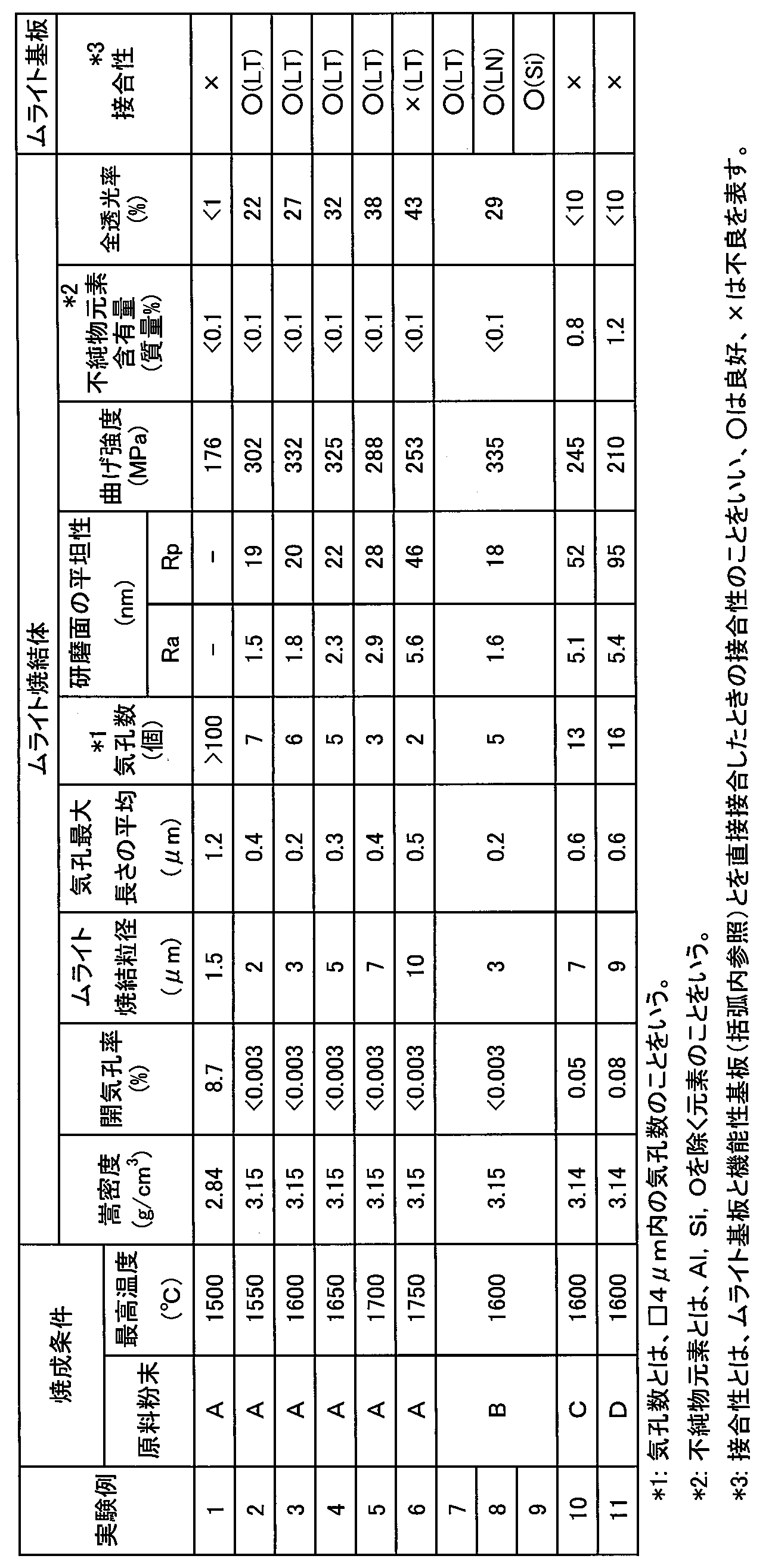
原料粉末Bを用い、実験例3と同様な方法でホットプレス焼成を行うことによりムライト焼結体を作製した。焼結体の嵩密度は3.15g/cm3で高く、開気孔率は0.03%未満で低く、十分緻密化していた。研磨面による焼結粒径、気孔長さ、気孔数、Ra、Rpとも実験例3と同様に小さく、良好であった。結晶相もムライト以外は検出されなかった。このムライト焼結体から3枚のムライト基板を切り出した。1つめのムライト基板はLT基板と直接接合し(実験例7)、2つめのムライト基板はLN基板と直接接合し(実験例8)、3つめのムライト基板はSi基板と直接接合した。そうしたところ、いずれも接合面積割合がほぼ100%であり、非常に良好に接合していた。
実験例10,11では、それぞれ原料粉末C、Dを用い、実験例3と同様な方法でホットプレス焼成をし、ムライト焼結体を作製した。いずれのムライト焼結体も、嵩密度は高く緻密化は進んでいるが、開気孔率がやや高くなっていることから焼結体内部に気孔が閉じ込められた状態であることがわかる。ムライト焼結粒の平均粒径も実験例3に比べ大きくなっており、原料に含有された不純物元素が焼結過程での粒成長を促進した可能性が考えられる。研磨仕上げ面のRa、Rpは共に大きく、粒成長が進んだこと、結晶相解析よりムライトに帰属できない小さなピークが見られたことから、不純物元素が異相部となって研磨面で凸状に存在していることが考えられる。これらは複合基板の支持基板には不適であると判断した。
Claims (9)
- 不純物元素の含有量が1質量%以下のムライト焼結体であって、
ムライト焼結粒の平均粒径が8μm以下であり、研磨仕上げした表面に存在する気孔の最大部長さの平均が0.4μm以下である、ムライト焼結体。 - 前記表面の中心線平均粗さ(Ra)が3nm以下である、請求項1に記載のムライト焼結体。
- 前記表面の最大高さ(Rp)が30nm以下である、請求項1又は2に記載のムライト焼結体。
- 前記表面に存在する気孔数が、4μm×4μmの面積当たり、10個以下である、請求項1~3のいずれか1項に記載のムライト焼結体。
- 四点曲げ強度が280MPa以上である、請求項1~4のいずれか1項記載のムライト焼結体。
- 不純物元素の含有量が0.5質量%以下である、請求項1~5のいずれか1項に記載のムライト焼結体。
- 前記ムライト焼結体を厚さ0.1mmの板状体としたときの波長550nmの光に対する全透光率が20%以上である、請求項1~6のいずれか1項に記載のムライト焼結体。
- 純度が99.0質量%以上(但し、加熱により飛散する成分は不純物とみなさない)のムライト原料粉末を所定形状に成形したのち、プレス圧力を20~300kgf/cm2、焼成温度を1525~1700℃に設定してホットプレス焼成を行うことによりムライト焼結体を得る、
ムライト焼結体の製法。 - 支持基板と機能性基板とが接合された複合基板であって、
前記支持基板は、請求項1~7のいずれか1項に記載のムライト焼結体からなるムライト基板である、複合基板。
Priority Applications (5)
| Application Number | Priority Date | Filing Date | Title |
|---|---|---|---|
| CN201580002212.6A CN105636920B (zh) | 2014-06-06 | 2015-05-26 | 莫来石烧结体、其制法以及复合基板 |
| JP2015547179A JP5861016B1 (ja) | 2014-06-06 | 2015-05-26 | ムライト焼結体、その製法及び複合基板 |
| KR1020167006367A KR101677415B1 (ko) | 2014-06-06 | 2015-05-26 | 멀라이트 소결체, 그 제법 및 복합 기판 |
| DE112015000148.4T DE112015000148B4 (de) | 2014-06-06 | 2015-05-26 | Verbundsubstrat und Verfahren zu dessen Herstellung |
| US15/064,968 US9776924B2 (en) | 2014-06-06 | 2016-03-09 | Mullite sintered body, method for producing the same, and composite substrate |
Applications Claiming Priority (4)
| Application Number | Priority Date | Filing Date | Title |
|---|---|---|---|
| JP2014-117926 | 2014-06-06 | ||
| JP2014117926 | 2014-06-06 | ||
| JP2015-053190 | 2015-03-17 | ||
| JP2015053190 | 2015-03-17 |
Related Child Applications (1)
| Application Number | Title | Priority Date | Filing Date |
|---|---|---|---|
| US15/064,968 Continuation US9776924B2 (en) | 2014-06-06 | 2016-03-09 | Mullite sintered body, method for producing the same, and composite substrate |
Publications (1)
| Publication Number | Publication Date |
|---|---|
| WO2015186560A1 true WO2015186560A1 (ja) | 2015-12-10 |
Family
ID=54766634
Family Applications (1)
| Application Number | Title | Priority Date | Filing Date |
|---|---|---|---|
| PCT/JP2015/065006 Ceased WO2015186560A1 (ja) | 2014-06-06 | 2015-05-26 | ムライト焼結体、その製法及び複合基板 |
Country Status (7)
| Country | Link |
|---|---|
| US (1) | US9776924B2 (ja) |
| JP (1) | JP5861016B1 (ja) |
| KR (1) | KR101677415B1 (ja) |
| CN (1) | CN105636920B (ja) |
| DE (1) | DE112015000148B4 (ja) |
| TW (1) | TWI570091B (ja) |
| WO (1) | WO2015186560A1 (ja) |
Cited By (7)
| Publication number | Priority date | Publication date | Assignee | Title |
|---|---|---|---|---|
| WO2016159393A1 (ja) * | 2016-03-22 | 2016-10-06 | 住友電気工業株式会社 | セラミック基板、積層体およびsawデバイス |
| KR20170104894A (ko) * | 2016-03-08 | 2017-09-18 | 국민대학교산학협력단 | 내환경 코팅재가 코팅된 구조체 및 상기 내환경 코팅재를 코팅하는 방법. |
| CN107226690A (zh) * | 2016-03-23 | 2017-10-03 | 日本碍子株式会社 | 含有多铝红柱石的烧结体、其制法及复合基板 |
| JP2018201017A (ja) * | 2017-05-29 | 2018-12-20 | 京セラ株式会社 | セラミック配線基板、プローブ基板およびプローブカード |
| JP2019140697A (ja) * | 2017-08-25 | 2019-08-22 | 日本碍子株式会社 | 接合体および弾性波素子 |
| US10931256B2 (en) | 2017-08-25 | 2021-02-23 | Ngk Insulators, Ltd. | Joined body and elastic wave element |
| JP6989722B1 (ja) * | 2021-03-31 | 2022-01-05 | 株式会社ニッカトー | 耐熱性及び耐久性にすぐれたムライト焼結体及びその製造方法 |
Families Citing this family (2)
| Publication number | Priority date | Publication date | Assignee | Title |
|---|---|---|---|---|
| US9905459B1 (en) | 2016-09-01 | 2018-02-27 | International Business Machines Corporation | Neutral atom beam nitridation for copper interconnect |
| CN112624774B (zh) * | 2020-12-21 | 2022-12-13 | 马鞍山利尔开元新材料有限公司 | 一种金属陶瓷转炉挡渣滑板砖材料及制备方法 |
Citations (10)
| Publication number | Priority date | Publication date | Assignee | Title |
|---|---|---|---|---|
| JPS60161371A (ja) * | 1984-02-01 | 1985-08-23 | 工業技術院長 | 高強度セラミツクス焼結体の製造法 |
| JPS6246955A (ja) * | 1985-08-26 | 1987-02-28 | ハリマセラミック株式会社 | ムライト焼結体の製造方法 |
| JPS6256356A (ja) * | 1985-09-04 | 1987-03-12 | 株式会社ノリタケカンパニーリミテド | ムライト焼結体の製造方法 |
| JPS6291464A (ja) * | 1985-10-15 | 1987-04-25 | 工業技術院長 | 透光性アルミナ・シリカ系セラミツクス焼結体の製造方法 |
| JPH03247557A (ja) * | 1985-05-30 | 1991-11-05 | Agency Of Ind Science & Technol | 高温強度が優れたアルミナ・シリカ系セラミックス焼結体の製造方法 |
| JPH04175264A (ja) * | 1990-08-17 | 1992-06-23 | Chichibu Cement Co Ltd | ムライト質焼結体の原料粉末及びムライト質焼結体の製造方法 |
| JPH06100358A (ja) * | 1992-09-18 | 1994-04-12 | Toyota Central Res & Dev Lab Inc | ムライト質焼結体の製造方法 |
| JPH06227859A (ja) * | 1993-02-03 | 1994-08-16 | Nitsukatoo:Kk | 耐熱性ムライト焼結体 |
| JP2001127362A (ja) * | 1999-10-29 | 2001-05-11 | Mitsui Kozan Material Kk | 固体レーザ発振器用反射筒 |
| JP2013155075A (ja) * | 2012-01-30 | 2013-08-15 | Sumitomo Electric Ind Ltd | 複合酸化物焼結体の製造方法 |
Family Cites Families (8)
| Publication number | Priority date | Publication date | Assignee | Title |
|---|---|---|---|---|
| JPH0611667B2 (ja) | 1985-05-30 | 1994-02-16 | 工業技術院長 | 高温強度が優れたアルミナ・シリカ系セラミックス焼結体の製造方法 |
| JPS6389455A (ja) * | 1986-10-01 | 1988-04-20 | 東レ株式会社 | ムライト焼結体 |
| WO2005039263A1 (ja) | 2003-10-17 | 2005-04-28 | Hitachi Metals, Ltd. | 多層セラミック基板及びその製造方法並びにこれを用いた電子機器 |
| BRPI0515824B1 (pt) * | 2004-11-03 | 2015-12-15 | Velocys Inc | ebulição parcial em mini e microcanais |
| CN1699271A (zh) * | 2005-05-23 | 2005-11-23 | 盐城工学院 | 用机械力化学法低温制备高纯莫来石的方法 |
| CN102320616A (zh) * | 2011-06-18 | 2012-01-18 | 福建师范大学 | 一种莫来石材料的原料配方及其制备方法 |
| JP5585570B2 (ja) | 2011-12-01 | 2014-09-10 | 住友電気工業株式会社 | ムライトを主成分とする焼結体 |
| US9136337B2 (en) * | 2012-10-12 | 2015-09-15 | Sumitomo Electric Industries, Ltd. | Group III nitride composite substrate and method for manufacturing the same, laminated group III nitride composite substrate, and group III nitride semiconductor device and method for manufacturing the same |
-
2015
- 2015-05-26 KR KR1020167006367A patent/KR101677415B1/ko active Active
- 2015-05-26 WO PCT/JP2015/065006 patent/WO2015186560A1/ja not_active Ceased
- 2015-05-26 CN CN201580002212.6A patent/CN105636920B/zh active Active
- 2015-05-26 DE DE112015000148.4T patent/DE112015000148B4/de active Active
- 2015-05-26 JP JP2015547179A patent/JP5861016B1/ja active Active
- 2015-05-28 TW TW104117122A patent/TWI570091B/zh active
-
2016
- 2016-03-09 US US15/064,968 patent/US9776924B2/en active Active
Patent Citations (10)
| Publication number | Priority date | Publication date | Assignee | Title |
|---|---|---|---|---|
| JPS60161371A (ja) * | 1984-02-01 | 1985-08-23 | 工業技術院長 | 高強度セラミツクス焼結体の製造法 |
| JPH03247557A (ja) * | 1985-05-30 | 1991-11-05 | Agency Of Ind Science & Technol | 高温強度が優れたアルミナ・シリカ系セラミックス焼結体の製造方法 |
| JPS6246955A (ja) * | 1985-08-26 | 1987-02-28 | ハリマセラミック株式会社 | ムライト焼結体の製造方法 |
| JPS6256356A (ja) * | 1985-09-04 | 1987-03-12 | 株式会社ノリタケカンパニーリミテド | ムライト焼結体の製造方法 |
| JPS6291464A (ja) * | 1985-10-15 | 1987-04-25 | 工業技術院長 | 透光性アルミナ・シリカ系セラミツクス焼結体の製造方法 |
| JPH04175264A (ja) * | 1990-08-17 | 1992-06-23 | Chichibu Cement Co Ltd | ムライト質焼結体の原料粉末及びムライト質焼結体の製造方法 |
| JPH06100358A (ja) * | 1992-09-18 | 1994-04-12 | Toyota Central Res & Dev Lab Inc | ムライト質焼結体の製造方法 |
| JPH06227859A (ja) * | 1993-02-03 | 1994-08-16 | Nitsukatoo:Kk | 耐熱性ムライト焼結体 |
| JP2001127362A (ja) * | 1999-10-29 | 2001-05-11 | Mitsui Kozan Material Kk | 固体レーザ発振器用反射筒 |
| JP2013155075A (ja) * | 2012-01-30 | 2013-08-15 | Sumitomo Electric Ind Ltd | 複合酸化物焼結体の製造方法 |
Cited By (19)
| Publication number | Priority date | Publication date | Assignee | Title |
|---|---|---|---|---|
| KR102054373B1 (ko) * | 2016-03-08 | 2019-12-10 | 국민대학교산학협력단 | 내환경 코팅재가 코팅된 구조체 및 상기 내환경 코팅재를 코팅하는 방법. |
| KR20170104894A (ko) * | 2016-03-08 | 2017-09-18 | 국민대학교산학협력단 | 내환경 코팅재가 코팅된 구조체 및 상기 내환경 코팅재를 코팅하는 방법. |
| CN107406335A (zh) * | 2016-03-22 | 2017-11-28 | 住友电气工业株式会社 | 陶瓷基板、层叠体和saw器件 |
| JP7095785B2 (ja) | 2016-03-22 | 2022-07-05 | 住友電気工業株式会社 | セラミック基板、積層体およびsawデバイス |
| WO2016159393A1 (ja) * | 2016-03-22 | 2016-10-06 | 住友電気工業株式会社 | セラミック基板、積層体およびsawデバイス |
| JP2021170782A (ja) * | 2016-03-22 | 2021-10-28 | 住友電気工業株式会社 | セラミック基板、積層体およびsawデバイス |
| US10340886B2 (en) | 2016-03-22 | 2019-07-02 | Sumitomo Electric Industries, Ltd. | Ceramic substrate, layered body, and saw device |
| CN107226690A (zh) * | 2016-03-23 | 2017-10-03 | 日本碍子株式会社 | 含有多铝红柱石的烧结体、其制法及复合基板 |
| CN107226690B (zh) * | 2016-03-23 | 2021-06-29 | 日本碍子株式会社 | 含有多铝红柱石的烧结体、其制法及复合基板 |
| KR102377657B1 (ko) * | 2016-03-23 | 2022-03-24 | 엔지케이 인슐레이터 엘티디 | 멀라이트 함유 소결체, 그 제법 및 복합 기판 |
| KR20170110526A (ko) * | 2016-03-23 | 2017-10-11 | 엔지케이 인슐레이터 엘티디 | 멀라이트 함유 소결체, 그 제법 및 복합 기판 |
| DE102017002808B4 (de) | 2016-03-23 | 2026-05-28 | Ngk Insulators, Ltd. | Mullit-enthaltender Sinterkörper, Verfahren zur Herstellung desselben und Verwendung des Mullit-enthaltenden Sinterkörpers als ein Trägersubstrat in einem Verbundwerkstoffsubstrat |
| JP2018201017A (ja) * | 2017-05-29 | 2018-12-20 | 京セラ株式会社 | セラミック配線基板、プローブ基板およびプローブカード |
| JP7093227B2 (ja) | 2017-05-29 | 2022-06-29 | 京セラ株式会社 | セラミック配線基板、プローブ基板およびプローブカード |
| JP2019140697A (ja) * | 2017-08-25 | 2019-08-22 | 日本碍子株式会社 | 接合体および弾性波素子 |
| US10931256B2 (en) | 2017-08-25 | 2021-02-23 | Ngk Insulators, Ltd. | Joined body and elastic wave element |
| US11637541B2 (en) | 2017-08-25 | 2023-04-25 | Ngk Insulators, Ltd. | Joined body and elastic wave element |
| JP6989722B1 (ja) * | 2021-03-31 | 2022-01-05 | 株式会社ニッカトー | 耐熱性及び耐久性にすぐれたムライト焼結体及びその製造方法 |
| JP2022156925A (ja) * | 2021-03-31 | 2022-10-14 | 株式会社ニッカトー | 耐熱性及び耐久性にすぐれたムライト焼結体及びその製造方法 |
Also Published As
| Publication number | Publication date |
|---|---|
| TW201609600A (zh) | 2016-03-16 |
| DE112015000148T5 (de) | 2016-05-19 |
| DE112015000148B4 (de) | 2023-11-02 |
| KR20160032270A (ko) | 2016-03-23 |
| KR101677415B1 (ko) | 2016-11-17 |
| CN105636920A (zh) | 2016-06-01 |
| TWI570091B (zh) | 2017-02-11 |
| JP5861016B1 (ja) | 2016-02-16 |
| JPWO2015186560A1 (ja) | 2017-04-20 |
| US9776924B2 (en) | 2017-10-03 |
| US20160185668A1 (en) | 2016-06-30 |
| CN105636920B (zh) | 2017-11-14 |
Similar Documents
| Publication | Publication Date | Title |
|---|---|---|
| JP5861016B1 (ja) | ムライト焼結体、その製法及び複合基板 | |
| JP5890945B1 (ja) | コージェライト焼結体、その製法、複合基板及び電子デバイス | |
| JP6681461B2 (ja) | 複合基板,その製法及び電子デバイス | |
| US11198648B2 (en) | Cordierite-based sintered body, method for producing the same, and composite substrate | |
| TWI762509B (zh) | 矽鋁氮氧化物燒結體、其製法、複合基板及電子元件 | |
| JP6940959B2 (ja) | コージェライト質焼結体、その製法及び複合基板 | |
| TWI718275B (zh) | 含富鋁紅柱石燒結體、其製法及複合基板 | |
| JP7018267B2 (ja) | サイアロン焼結体、その製法、複合基板及び電子デバイス |
Legal Events
| Date | Code | Title | Description |
|---|---|---|---|
| ENP | Entry into the national phase |
Ref document number: 2015547179 Country of ref document: JP Kind code of ref document: A |
|
| 121 | Ep: the epo has been informed by wipo that ep was designated in this application |
Ref document number: 15804009 Country of ref document: EP Kind code of ref document: A1 |
|
| ENP | Entry into the national phase |
Ref document number: 20167006367 Country of ref document: KR Kind code of ref document: A |
|
| WWE | Wipo information: entry into national phase |
Ref document number: 1120150001484 Country of ref document: DE Ref document number: 112015000148 Country of ref document: DE |
|
| 122 | Ep: pct application non-entry in european phase |
Ref document number: 15804009 Country of ref document: EP Kind code of ref document: A1 |