WO2015163379A1 - ネガ型感光性樹脂組成物、隔壁および光学素子 - Google Patents
ネガ型感光性樹脂組成物、隔壁および光学素子 Download PDFInfo
- Publication number
- WO2015163379A1 WO2015163379A1 PCT/JP2015/062288 JP2015062288W WO2015163379A1 WO 2015163379 A1 WO2015163379 A1 WO 2015163379A1 JP 2015062288 W JP2015062288 W JP 2015062288W WO 2015163379 A1 WO2015163379 A1 WO 2015163379A1
- Authority
- WO
- WIPO (PCT)
- Prior art keywords
- resin composition
- photosensitive resin
- group
- ink
- partition
- Prior art date
- Legal status (The legal status is an assumption and is not a legal conclusion. Google has not performed a legal analysis and makes no representation as to the accuracy of the status listed.)
- Ceased
Links
Images


Classifications
-
- G—PHYSICS
- G03—PHOTOGRAPHY; CINEMATOGRAPHY; ANALOGOUS TECHNIQUES USING WAVES OTHER THAN OPTICAL WAVES; ELECTROGRAPHY; HOLOGRAPHY
- G03F—PHOTOMECHANICAL PRODUCTION OF TEXTURED OR PATTERNED SURFACES, e.g. FOR PRINTING, FOR PROCESSING OF SEMICONDUCTOR DEVICES; MATERIALS THEREFOR; ORIGINALS THEREFOR; APPARATUS SPECIALLY ADAPTED THEREFOR
- G03F7/00—Photomechanical, e.g. photolithographic, production of textured or patterned surfaces, e.g. printing surfaces; Materials therefor, e.g. comprising photoresists; Apparatus specially adapted therefor
- G03F7/004—Photosensitive materials
- G03F7/038—Macromolecular compounds which are rendered insoluble or differentially wettable
- G03F7/0382—Macromolecular compounds which are rendered insoluble or differentially wettable the macromolecular compound being present in a chemically amplified negative photoresist composition
-
- G—PHYSICS
- G02—OPTICS
- G02B—OPTICAL ELEMENTS, SYSTEMS OR APPARATUS
- G02B5/00—Optical elements other than lenses
- G02B5/20—Filters
-
- G—PHYSICS
- G02—OPTICS
- G02F—OPTICAL DEVICES OR ARRANGEMENTS FOR THE CONTROL OF LIGHT BY MODIFICATION OF THE OPTICAL PROPERTIES OF THE MEDIA OF THE ELEMENTS INVOLVED THEREIN; NON-LINEAR OPTICS; FREQUENCY-CHANGING OF LIGHT; OPTICAL LOGIC ELEMENTS; OPTICAL ANALOGUE/DIGITAL CONVERTERS
- G02F1/00—Devices or arrangements for the control of the intensity, colour, phase, polarisation or direction of light arriving from an independent light source, e.g. switching, gating or modulating; Non-linear optics
- G02F1/01—Devices or arrangements for the control of the intensity, colour, phase, polarisation or direction of light arriving from an independent light source, e.g. switching, gating or modulating; Non-linear optics for the control of the intensity, phase, polarisation or colour
- G02F1/13—Devices or arrangements for the control of the intensity, colour, phase, polarisation or direction of light arriving from an independent light source, e.g. switching, gating or modulating; Non-linear optics for the control of the intensity, phase, polarisation or colour based on liquid crystals, e.g. single liquid crystal display cells
- G02F1/133—Constructional arrangements; Operation of liquid crystal cells; Circuit arrangements
- G02F1/1333—Constructional arrangements; Manufacturing methods
- G02F1/1335—Structural association of cells with optical devices, e.g. polarisers or reflectors
-
- G—PHYSICS
- G03—PHOTOGRAPHY; CINEMATOGRAPHY; ANALOGOUS TECHNIQUES USING WAVES OTHER THAN OPTICAL WAVES; ELECTROGRAPHY; HOLOGRAPHY
- G03F—PHOTOMECHANICAL PRODUCTION OF TEXTURED OR PATTERNED SURFACES, e.g. FOR PRINTING, FOR PROCESSING OF SEMICONDUCTOR DEVICES; MATERIALS THEREFOR; ORIGINALS THEREFOR; APPARATUS SPECIALLY ADAPTED THEREFOR
- G03F7/00—Photomechanical, e.g. photolithographic, production of textured or patterned surfaces, e.g. printing surfaces; Materials therefor, e.g. comprising photoresists; Apparatus specially adapted therefor
- G03F7/004—Photosensitive materials
-
- G—PHYSICS
- G03—PHOTOGRAPHY; CINEMATOGRAPHY; ANALOGOUS TECHNIQUES USING WAVES OTHER THAN OPTICAL WAVES; ELECTROGRAPHY; HOLOGRAPHY
- G03F—PHOTOMECHANICAL PRODUCTION OF TEXTURED OR PATTERNED SURFACES, e.g. FOR PRINTING, FOR PROCESSING OF SEMICONDUCTOR DEVICES; MATERIALS THEREFOR; ORIGINALS THEREFOR; APPARATUS SPECIALLY ADAPTED THEREFOR
- G03F7/00—Photomechanical, e.g. photolithographic, production of textured or patterned surfaces, e.g. printing surfaces; Materials therefor, e.g. comprising photoresists; Apparatus specially adapted therefor
- G03F7/004—Photosensitive materials
- G03F7/038—Macromolecular compounds which are rendered insoluble or differentially wettable
-
- G—PHYSICS
- G03—PHOTOGRAPHY; CINEMATOGRAPHY; ANALOGOUS TECHNIQUES USING WAVES OTHER THAN OPTICAL WAVES; ELECTROGRAPHY; HOLOGRAPHY
- G03F—PHOTOMECHANICAL PRODUCTION OF TEXTURED OR PATTERNED SURFACES, e.g. FOR PRINTING, FOR PROCESSING OF SEMICONDUCTOR DEVICES; MATERIALS THEREFOR; ORIGINALS THEREFOR; APPARATUS SPECIALLY ADAPTED THEREFOR
- G03F7/00—Photomechanical, e.g. photolithographic, production of textured or patterned surfaces, e.g. printing surfaces; Materials therefor, e.g. comprising photoresists; Apparatus specially adapted therefor
- G03F7/004—Photosensitive materials
- G03F7/075—Silicon-containing compounds
-
- H—ELECTRICITY
- H05—ELECTRIC TECHNIQUES NOT OTHERWISE PROVIDED FOR
- H05B—ELECTRIC HEATING; ELECTRIC LIGHT SOURCES NOT OTHERWISE PROVIDED FOR; CIRCUIT ARRANGEMENTS FOR ELECTRIC LIGHT SOURCES, IN GENERAL
- H05B33/00—Electroluminescent light sources
- H05B33/12—Light sources with substantially two-dimensional [2D] radiating surfaces
-
- H—ELECTRICITY
- H05—ELECTRIC TECHNIQUES NOT OTHERWISE PROVIDED FOR
- H05B—ELECTRIC HEATING; ELECTRIC LIGHT SOURCES NOT OTHERWISE PROVIDED FOR; CIRCUIT ARRANGEMENTS FOR ELECTRIC LIGHT SOURCES, IN GENERAL
- H05B33/00—Electroluminescent light sources
- H05B33/12—Light sources with substantially two-dimensional [2D] radiating surfaces
- H05B33/22—Light sources with substantially two-dimensional [2D] radiating surfaces characterised by the chemical or physical composition or the arrangement of auxiliary dielectric or reflective layers
-
- H—ELECTRICITY
- H10—SEMICONDUCTOR DEVICES; ELECTRIC SOLID-STATE DEVICES NOT OTHERWISE PROVIDED FOR
- H10F—INORGANIC SEMICONDUCTOR DEVICES SENSITIVE TO INFRARED RADIATION, LIGHT, ELECTROMAGNETIC RADIATION OF SHORTER WAVELENGTH OR CORPUSCULAR RADIATION
- H10F19/00—Integrated devices, or assemblies of multiple devices, comprising at least one photovoltaic cell covered by group H10F10/00, e.g. photovoltaic modules
- H10F19/30—Integrated devices, or assemblies of multiple devices, comprising at least one photovoltaic cell covered by group H10F10/00, e.g. photovoltaic modules comprising thin-film photovoltaic cells
-
- H—ELECTRICITY
- H10—SEMICONDUCTOR DEVICES; ELECTRIC SOLID-STATE DEVICES NOT OTHERWISE PROVIDED FOR
- H10K—ORGANIC ELECTRIC SOLID-STATE DEVICES
- H10K50/00—Organic light-emitting devices
-
- H—ELECTRICITY
- H10—SEMICONDUCTOR DEVICES; ELECTRIC SOLID-STATE DEVICES NOT OTHERWISE PROVIDED FOR
- H10K—ORGANIC ELECTRIC SOLID-STATE DEVICES
- H10K50/00—Organic light-emitting devices
- H10K50/10—OLEDs or polymer light-emitting diodes [PLED]
- H10K50/11—OLEDs or polymer light-emitting diodes [PLED] characterised by the electroluminescent [EL] layers
- H10K50/115—OLEDs or polymer light-emitting diodes [PLED] characterised by the electroluminescent [EL] layers comprising active inorganic nanostructures, e.g. luminescent quantum dots
-
- Y—GENERAL TAGGING OF NEW TECHNOLOGICAL DEVELOPMENTS; GENERAL TAGGING OF CROSS-SECTIONAL TECHNOLOGIES SPANNING OVER SEVERAL SECTIONS OF THE IPC; TECHNICAL SUBJECTS COVERED BY FORMER USPC CROSS-REFERENCE ART COLLECTIONS [XRACs] AND DIGESTS
- Y02—TECHNOLOGIES OR APPLICATIONS FOR MITIGATION OR ADAPTATION AGAINST CLIMATE CHANGE
- Y02E—REDUCTION OF GREENHOUSE GAS [GHG] EMISSIONS, RELATED TO ENERGY GENERATION, TRANSMISSION OR DISTRIBUTION
- Y02E10/00—Energy generation through renewable energy sources
- Y02E10/50—Photovoltaic [PV] energy
Definitions
- the present invention relates to a negative photosensitive resin composition, a partition, and an optical element.
- an organic layer such as a light emitting layer is used as a dot by an inkjet (IJ) method.
- IJ inkjet
- a pattern printing method may be used. In such a method, a partition is provided along the outline of the dot to be formed, and an ink containing the material of the organic layer is injected into a partition (hereinafter also referred to as “opening”) surrounded by the partition. This is dried and / or heated to form dots having a desired pattern.
- the upper surface of the partition wall has ink repellency to prevent mixing of ink between adjacent dots and the uniform application of ink in the formation of dots, while for dot formation surrounded by the partition wall including the partition wall side surface.
- the opening needs to have ink affinity.
- a method of forming a partition corresponding to a dot pattern by a photolithography method using a photosensitive resin composition containing an ink repellent agent is known.
- the photosensitive resin is roughly classified into radical polymerization type photosensitive resins and cationic polymerization type photosensitive resins.
- the radical polymerization type photosensitive resin composition it is known that curing of the outermost surface is inhibited by oxygen. Therefore, in order to develop sufficient ink repellency on the outermost surface using a photosensitive resin composition containing an ink repellent agent, a large amount of exposure is required. As a result, sensitivity, patterning shape The residue may be affected.
- Patent Document 1 includes a structural unit derived from an unsaturated compound having a fluoroalkyl group having 4 to 6 carbon atoms. A composition is described in which a liquid repellent composed of an addition polymer and a cationic polymerization type photosensitive resin are combined.
- the liquid repellent described in Patent Document 1 is fixed to the surface of the partition wall with a small exposure amount at the time of forming the partition wall, but is performed for the purpose of removing impurities remaining on the dots after the partition wall formation, for example, a cleaning process using an alkaline aqueous solution Insufficient resistance to ink-philic treatment such as ultraviolet cleaning treatment, ultraviolet / ozone cleaning treatment, excimer cleaning treatment, corona discharge treatment and oxygen plasma treatment.
- the present invention has been made from the above viewpoint, and it is possible to form an ink-repellent layer having sufficient ink repellency at a low exposure amount on the upper surface of the partition wall, and the ink-repellent layer has undergone an ink affinity treatment.
- Another object of the present invention is to provide a negative photosensitive resin composition that can be used for the production of a partition wall that can maintain excellent ink repellency.
- the present invention is a partition wall having an ink repellent layer having sufficient ink repellency on the upper surface and capable of forming a fine and highly accurate pattern, and maintains excellent ink repellency even after being subjected to a lyophilic process.
- An object of the present invention is to provide a partition wall for an optical element.
- the present invention provides an optical element having dots formed by applying ink uniformly to the openings partitioned by the partition walls, specifically, an organic EL element, a quantum dot display, a TFT array, or a thin film solar. The purpose is to provide batteries.
- the present invention provides a negative photosensitive resin composition, partition walls, and optical elements having the following configurations [1] to [15].
- a negative photosensitive resin composition comprising an ink repellent agent (D) containing s1) as a monomer and / or a partially hydrolyzed (co) condensate.
- D ink repellent agent
- the ink repellent agent (D) contains a hydrolyzable silane compound (s2) in which four hydrolyzable groups are bonded to a silicon atom as a monomer and / or a partially hydrolyzed (co) condensate.
- the negative photosensitive resin composition as described in [1] or [2] above.
- the ink repellent agent (D) contains a hydrolyzable silane compound (s3) having only a hydrocarbon group and a hydrolyzable group as a monomer and / or a partially hydrolyzed (co) condensate.
- the negative photosensitive resin composition according to any one of [1] to [3].
- the ink repellent agent (D) comprises a hydrolyzable silane compound (s4) having a cationic polymerizable group and a hydrolyzable group and containing no fluorine atom as a monomer and / or partially hydrolyzed (co-polymerized).
- the negative photosensitive resin composition according to any one of the above [1] to [4], which is contained as a condensate.
- the content of the alkali-soluble resin (A) is 10 to 90% by mass in the total solid content in the negative photosensitive resin composition.
- the negative photosensitive resin composition as described.
- the content of the crosslinking agent (B) and the photoacid generator is 2 to 50 parts by mass and 0.1 to 20 parts by mass, respectively, with respect to 100 parts by mass of the alkali-soluble resin (A).
- the negative photosensitive resin composition according to any one of the above [1] to [6]. [8] Any one of the above [1] to [7], wherein the content of the ink repellent agent (D) is 0.01 to 20 parts by mass with respect to 100 parts by mass of the alkali-soluble resin (A). Negative photosensitive resin composition as described in the item.
- the optical element is an organic EL element, a quantum dot display, a TFT array, or a thin film solar cell.
- the negative photosensitive resin composition of the present invention By using the negative photosensitive resin composition of the present invention, it is possible to form an ink repellent layer having sufficient ink repellency at a low exposure amount on the upper surface of the partition wall, and the ink repellent layer is subjected to an ink affinity treatment. Even after passing, it is possible to produce partition walls that can maintain excellent ink repellency.
- the partition wall of the present invention has an ink repellent layer having sufficient ink repellency on the upper surface, can form a fine and highly accurate pattern, and the ink is evenly distributed in the openings partitioned by the partition wall.
- An organic EL element, a quantum dot display, a TFT array, or a thin-film solar cell using an optical element having dots that are coated on and accurately formed can be provided.
- (Meth) acryloyl group is a general term for “methacryloyl group” and “acryloyl group”.
- the (meth) acryloyloxy group, (meth) acrylic acid, (meth) acrylate, (meth) acrylamide, and (meth) acrylic resin also conform to this.
- the group represented by the formula (x) may be simply referred to as a group (x).
- the compound represented by the formula (y) may be simply referred to as the compound (y).
- the expressions (x) and (y) indicate arbitrary expressions.
- the “side chain” is a group other than a hydrogen atom or a halogen atom bonded to a carbon atom constituting the main chain in a polymer in which a repeating unit composed of carbon atoms constitutes the main chain.
- “Unit” such as a fluorine atom-containing unit indicates a polymerized unit.
- the “total solid content of the photosensitive resin composition” refers to a component that forms a cured film, which will be described later, among the components contained in the photosensitive resin composition.
- the photosensitive resin composition is heated at 140 ° C. for 24 hours. Determine from the residue after removing the solvent. The total solid content can also be calculated from the charged amount.
- a film made of a cured product of a composition containing resin as a main component is referred to as a “resin cured film”.
- a film coated with the photosensitive resin composition is referred to as a “coating film”, and a film obtained by drying the film is referred to as a “dry film”.
- a film obtained by curing the “dry film” is a “resin cured film”. Further, the “resin cured film” may be simply referred to as “cured film”.
- the “partition wall” is a form of a cured resin film formed in a shape that partitions a predetermined region into a plurality of sections. For example, the following “ink” is injected into the partitions partitioned by the partition walls, that is, the openings surrounded by the partition walls to form “dots”.
- “Ink” is a generic term for liquids that have optical and / or electrical functions after drying, curing, and the like.
- an optical element such as an organic EL element, a color filter of a liquid crystal element, and a TFT (Thin Film Transistor) array
- dots as various components are pattern-printed by using an ink for forming the dots by an inkjet (IJ) method.
- IJ inkjet
- “Ink” includes ink used in such applications.
- “Ink repellency” is a property of repelling the above ink and has both water repellency and oil repellency.
- the ink repellency can be evaluated by, for example, a contact angle when ink is dropped.
- “Ink affinity” is a property opposite to ink repellency, and can be evaluated by the contact angle when ink is dropped as in the case of ink repellency.
- the ink affinity can be evaluated by evaluating the degree of ink wetting and spreading (ink wetting and spreading property) when ink is dropped on a predetermined standard.
- Dot indicates the minimum area where optical modulation is possible in the optical element.
- the negative photosensitive resin composition of the present invention comprises an alkali-soluble resin (A), a crosslinking agent (B), a photoacid generator (C), a fluoroalkylene group and / or a fluoroalkyl group, and a hydrolyzable group. And an ink repellent agent (D) containing a hydrolyzable silane compound (s1) having a monomer and / or a partially hydrolyzed (co) condensate.
- the negative photosensitive resin composition of the present invention further contains a solvent (E) and other optional components as necessary.
- Alkali-soluble resin (A) As alkali-soluble resin (A) in the negative photosensitive resin composition of this invention, it couple
- Any cationic polymerization type alkali-soluble resin (A) that is crosslinked and insoluble in alkali can be used without particular limitation.
- alkali-soluble resin (A) examples include phenols and aldehydes, and if necessary, unmodified or modified novolak-type phenol resins and vinylphenol resins (hereinafter referred to as “polyphenols”) produced by polycondensation with various modifiers. , “Polyvinylphenol”), N- (4-hydroxyphenyl) methacrylamide copolymers, hydroquinone monomethacrylate copolymers, and the like.
- various alkali-soluble polymer compounds such as sulfonylimide polymers, carboxyl group-containing polymers, acrylic resins containing phenolic hydroxyl groups, acrylic resins having sulfonamide groups, and urethane resins may be used. it can.
- alkali-soluble resin (A) a novolac type phenol resin or a vinyl phenol resin is preferable.
- phenols and aldehydes used for producing the novolak-type phenol resin include those described in International Publication No. 2013/133392, for example, in paragraphs [0021] and [0022].
- novolak type phenol resins using cresols, xylenols and the like are preferable as phenols from the viewpoints of easy availability and few metal impurities, and novolak type using cresols.
- Phenol resin (hereinafter also referred to as “cresol novolac resin”) is particularly preferable.
- polyvinylphenol examples include vinylphenol homopolymers, copolymers of vinylphenol and monomers copolymerizable therewith.
- Polyvinylphenol is a vinylphenol such as 4-vinylphenol, 3-vinylphenol, 2-vinylphenol, 2-methyl-4-vinylphenol, 2,6-dimethyl-4-vinylphenol, or a combination of two or more. Then, it can be obtained by radical polymerization using a polymerization initiator such as azobisisobutyronitrile or benzoyl peroxide.
- Examples of the monomer copolymerizable with vinylphenol include isopropenylphenol, acrylic acid, methacrylic acid, styrene, maleic anhydride, maleic imide, and vinyl acetate.
- a vinylphenol homopolymer is preferable, and a 4-vinylphenol homopolymer is particularly preferable.
- the mass average molecular weight (Mw) of the alkali-soluble resin (A) is preferably 500 to 20,000, particularly preferably 2,000 to 15,000. If the mass average molecular weight (Mw) of the alkali-soluble resin (A) is too low, the molecular weight does not increase sufficiently even if a cross-linking reaction occurs in the exposed region, so that it is easily dissolved in an alkali developer. If the mass average molecular weight (Mw) of the alkali-soluble resin (A) is too large, the difference in solubility in the alkali developer between the exposed area and the unexposed area becomes small, and it becomes difficult to obtain a good resist pattern.
- a mass average molecular weight (Mw) means the mass average molecular weight converted on the basis of standard polystyrene, which is measured by gel permeation chromatography (GPC) using tetrahydrofuran as a mobile phase.
- the number average molecular weight (Mn) means the number average molecular weight measured by the same GPC.
- alkali-soluble resin A
- cresol novolak resin examples include EP4020G (Mw: 9,000 to 14,000), EPR5010G (Mw: 7,000 to 12,000). 500) (above, trade name, manufactured by Asahi Organic Materials Co., Ltd.), and commercial products of polyvinylphenol include Marcalinker M (trade name, manufactured by Maruzen Petrochemical Co., Ltd.) and the like.
- Alkali-soluble resin (A) may be used individually by 1 type, or may use 2 or more types together.
- the content of the alkali-soluble resin (A) in the total solid content in the negative photosensitive resin composition is preferably 10 to 90% by mass, more preferably 30 to 85% by mass, and particularly preferably 40 to 80% by mass. When the content is in the above range, the developability of the negative photosensitive resin composition is improved.
- Crosslinking agent (B) The crosslinking agent (B) binds to the alkali-soluble resin (A) by the action of the acid generated by the photoacid generator (C) upon irradiation (exposure) with actinic rays, thereby converting the alkali-soluble resin (A). It is a compound (acid-sensitive substance) that can be rendered insoluble in alkali by crosslinking.
- crosslinking agent (B) examples include low molecular crosslinking agents such as melamine-based, benzoguanamine-based, urea-based and isocyanate-based compounds, polyfunctional epoxide group-containing compounds, oxetane-based compounds, alkoxyalkylated melamine resins or alkoxyalkylated ureas.
- Polymer crosslinking agents such as alkoxyalkylated amino resins such as resins are preferred.
- Examples of the melamine compounds include melamine, methoxymethylated melamine, ethoxymethylated melamine, propoxymethylated melamine, butoxymethylated melamine, hexamethylol melamine and the like.
- Examples of the benzoguanamine compound include benzoguanamine and methylated benzoguanamine.
- Examples of the urea compound include urea, monomethylol urea, dimethylol urea, alkoxymethylene urea, N-alkoxymethylene urea, ethylene urea, ethylene urea carboxylic acid, tetrakis (methoxymethyl) glycoluril and the like.
- isocyanate compound examples include hexamethylene diisocyanate, 1,4-cyclohexyl diisocyanate, toluene diisocyanate, bisisocyanate methylcyclohexane, bisisocyanate methylbenzene, and ethylene diisocyanate.
- the polyfunctional epoxide group-containing compound one containing one or more benzene rings or heterocyclic rings and two or more epoxy groups in one molecule is preferable.
- oxetane compound one containing two or more oxetanyl groups in one molecule is preferable.
- alkoxyalkylated melamine resin or alkoxyalkylated urea resin examples include methoxymethylated melamine resin, ethoxymethylated melamine resin, propoxymethylated melamine resin, butoxymethylated melamine resin, methoxymethylated urea resin, ethoxymethylated urea resin, Examples thereof include propoxymethylated urea resins and butoxymethylated urea resins.
- cross-linking agent (B) a commercially available product may be used.
- a commercially available product of alkoxymethylated amino resin PL-1170, PL-1174, UFR65, CYMEL300, CYMEL303 (manufactured by Mitsui Cytec) BX-4000, Nicalac MW-30, MX290, MW-100LM (manufactured by Sanwa Chemical Co., Ltd.) and the like.
- the crosslinking agent (B) can be used alone or in combination of two or more.
- the blending amount is preferably 2 to 50 parts by mass, more preferably 5 to 30 parts by mass, and further preferably 10 to 25 parts by mass with respect to 100 parts by mass of the alkali-soluble resin (A). If the amount of the crosslinking agent (B) used is too small, it is difficult for the crosslinking reaction to proceed sufficiently, and the residual film ratio of the resist pattern after development using an alkali developer decreases, Deformation such as meandering is likely to occur. When there is too much usage-amount of a crosslinking agent (B), there exists a possibility that the resolution may fall.
- the photoacid generator (C) is not particularly limited as long as it is a compound that decomposes to generate an acid upon irradiation with an actinic ray.
- an arbitrary compound can be selected from compounds generally used as a photoacid generator.
- the acid generated from the photoacid generator (C) is related to the bond between the alkali-soluble resin (A) and the crosslinking agent (B), and the ink repellent. It functions as a catalyst for the hydrolysis reaction of the fluorine-containing hydrolyzable silane compound (s1) contained in the agent (D).
- an acid catalyst is blended together with a composition containing a hydrolyzable silane compound. As a result, the reaction proceeds gradually and storage stability may become a problem.
- the photoacid generator (C) is decomposed by irradiation with actinic rays to generate an acid.
- the actinic rays include high energy rays such as ultraviolet light, X-rays, and electron beams.
- i line (365 nm), h line (405 nm), and g line (436 nm) are used preferably for exposure.
- the photoacid generator (C) it is preferable to select a photoacid generator having a large absorbance at the wavelength of light used for exposure.
- the photoacid generator examples include onium salt photoacid generators and nonionic photoacid generators.
- Examples of the onium salt photoacid generator include onium salts and iodonium salt compounds of a compound having a triphenylsulfonium skeleton represented by the following formula (C1) or (C2).
- C1 and C2 compounds in which the hydrogen atom of the phenyl group of the triphenylsulfonium skeleton is substituted can also be used as the photoacid generator.
- Xa - and Xb - represent anions.
- Specific examples include phosphorus anions such as PF 6 ⁇ , (R f1 ) n PF 6-n ⁇ (R f1 is a fluoroalkyl group, n is 1 to 3), and the like.
- Anions such as R a SO 3 — (R a is an alkyl group having 1 to 12 carbon atoms or an aryl group having 6 to 18 carbon atoms, part or all of which may be substituted with a fluorine atom). It is done.
- R a SO 3 - The a R a, for example, -CF 3, -C 4 F 9 , perfluoroalkyl groups such as -C 8 F 17, -C 6 F 5 , etc. perfluoroalkyl aryl group, -Ph-CH 3 (However, Ph represents a phenyl group.) And the like.
- the cation moiety absorbs the irradiated light, and the anion moiety becomes a source of acid generation.
- triphenylsulfonium / nonafluorobutanesulfonate represented by the following formula (C1-1)
- the triarylsulfonium / PF 6 salt and triarylsulfonium / special phosphorus salt represented by the following formulas (C2-1) and (C2-2) have large absorbance at a wavelength of 365 nm and are easily available. This is preferable.
- R f1 is a fluoroalkyl group, and n is 1 to 3.
- iodonium salt-based compounds examples include diphenyliodonium trifluoromethanesulfonate, trifluoromethanesulfonate (p-tert-butoxyphenyl) phenyliodonium, p-toluenesulfonate diphenyliodonium, p-toluenesulfonate (p-tert-butoxyphenyl). Examples thereof include phenyliodonium.
- TPSP-PFBS compound (C1-1), trade name, manufactured by Toyo Gosei Co., Ltd.
- CPI-100P compound (C2-1), trade name, manufactured by San Apro
- CPI-210S compound (C2- 2), trade name, manufactured by San Apro Co., Ltd.
- nonionic photoacid generator examples include a naphthalimide skeleton, a nitrobenzene skeleton, a diazomethane skeleton, a phenylacetophenone skeleton, a thiochitosan skeleton, a triazine skeleton, and a structure in which a chlorine atom, an alkanesulfonic acid, an arylsulfonic acid, or the like is bonded.
- a naphthalimide skeleton examples include a naphthalimide skeleton, a nitrobenzene skeleton, a diazomethane skeleton, a phenylacetophenone skeleton, a thiochitosan skeleton, a triazine skeleton, and a structure in which a chlorine atom, an alkanesulfonic acid, an arylsulfonic acid, or the like is bonded.
- the compound which has is mentioned.
- a naphthalimide skeleton represented by the following formula (C3), the following formula (C4), the following formula (C5), the following formula (C6), and the following formula (C7) respectively.
- a compound having a triazine skeleton and a chlorine atom represented by the following formula (C8) can be given.
- a sulfonyl compound of dialkylglyoxime represented by the following formula (C9) a sulfonyloxyiminoacetonitrile represented by the following formula (C10), and the like can be mentioned.
- a compound in which a hydrogen atom of a benzene ring forming the skeleton of each compound is substituted also has a function as a photoacid generator.
- R b1 to R b5 , R b7 and R b9 in formulas (C3) to (C7), (C9), and (C10) each independently may be partially or entirely substituted with a fluorine atom.
- It is a linear, branched or cyclic (including those having a partial cyclic structure) alkyl group having 1 to 12 carbon atoms or aryl group having 6 to 18 carbon atoms.
- Specific examples include perfluoroalkyl groups such as —CF 3 , —C 4 F 9 , —C 8 F 17 , perfluoroaryl groups such as —C 6 F 5 , aryl groups such as —Ph—CH 3, and the like. .
- R b6 , R b8 and R b10 in the formulas (C8), (C9) and (C10) are each independently an organic group having 1 to 18 carbon atoms which may have a substituent.
- a portion where a chlorine atom, alkane sulfonic acid, aryl sulfonic acid, or the like is bonded serves as an acid generation source.
- nonionic photoacid generator examples include N-trifluoromethanesulfonic acid-1,8 represented by the following formula (C3-1) as a compound used for performing exposure with i-line (365 nm).
- NHNI-TF compound (C3-1), trade name, manufactured by Toyo Gosei Co., Ltd.
- C3-1 compound (C3-1), trade name, manufactured by Toyo Gosei Co., Ltd.
- Acids generated by the action of light from these onium salt photoacid generators and nonionic photoacid generators are hydrochloric acid, alkane sulfonic acids, aryl sulfonic acids, and partially or fully fluorinated aryls. Examples thereof include sulfonic acid and alkane sulfonic acid.
- the photoacid generator (C) one type of the above compounds may be used alone, or two or more types may be used in combination.
- the content of the photoacid generator (C) is preferably 0.1 to 20 parts by weight, more preferably 0.5 to 10 parts by weight, based on 100 parts by weight of the alkali-soluble resin (A). Part is particularly preferred.
- the ink repellent agent (D) in the present invention contains a hydrolyzable silane compound (s1) having a fluoroalkylene group and / or a fluoroalkyl group and a hydrolyzable group.
- the ink repellent agent (D) may be a hydrolyzable silane compound (s1) or a hydrolyzable silane compound (s1) and any other hydrolyzable silane compound (s1) as an optional component to be described later. It is good also as a mixture with a silane compound.
- the ink repellent agent (D) is preferably composed only of a hydrolyzable silane compound containing the hydrolyzable silane compound (s1).
- the ink repellent agent (D) contains the hydrolyzable silane compound (s1) as a monomer and / or a partially hydrolyzed (co) condensate. That is, the ink repellent agent (D) may contain the hydrolyzable silane compound (s1) as a monomer or a partially hydrolyzed condensate thereof. Further, when the ink repellent agent (D) contains a hydrolyzable silane compound other than the hydrolyzable silane compound (s1), a portion of the hydrolyzable silane compound (s1) and the other hydrolyzable silane compound. You may contain as a hydrolysis (co) condensate.
- hydrolyzable silane compound (s1) is a mixture of two or more selected from monomers, partially hydrolyzed condensates thereof, and partially hydrolyzed (co) condensates with other hydrolyzable silane compounds. It may be contained in the ink repellent agent (D).
- the ink repellent agent (D) containing a specific hydrolyzable silane compound means containing the hydrolyzable silane compound as a monomer and / or a partially hydrolyzed (co) condensate.
- the “monomer and / or partially hydrolyzed (co) condensate” is the same as the range defined above.
- the ink repellent agent (D) forms a cured film using a negative photosensitive resin composition containing this. It has a property of shifting to the upper surface in the process (upper surface shifting property) and ink repellency.
- the ink repellent agent (D) By using the ink repellent agent (D), the upper layer portion including the upper surface of the obtained partition wall is a layer in which the ink repellent agent (D) is present densely (hereinafter also referred to as “ink repellent layer”). Ink repellency is imparted to the upper surface of the partition wall.
- Such an ink repellent layer is mainly formed from a cured product of a hydrolyzable silane compound containing a hydrolyzable silane compound (s1), and therefore, even after an ink-philic treatment such as an ultraviolet ray / ozone cleaning treatment. It is advantageous in that excellent ink repellency can be maintained.
- the content of fluorine atoms in the ink repellent agent (D) is preferably 1 to 40% by mass, more preferably 5 to 35% by mass, and particularly preferably 10 to 30% by mass, from the viewpoints of upper surface migration and ink repellency. preferable.
- the fluorine atom content of the ink repellent agent (D) is not less than the lower limit of the above range, good ink repellency can be imparted to the upper surface of the cured film, and when it is not more than the upper limit, the negative photosensitive resin composition Good compatibility with other components in the product.
- the ink repellent agent (D) is preferably a mixture (hereinafter also referred to as “mixture (M)”) consisting essentially of a hydrolyzable silane compound containing the hydrolyzable silane compound (s1). Or a partially hydrolyzed (co) condensate of the mixture (M).
- the mixture (M) contains a hydrolyzable silane compound (s1) having a fluoroalkylene group and / or a fluoroalkyl group and a hydrolyzable group as an essential component, and optionally other than the hydrolyzable silane compound (s1). Contains hydrolyzable silane compounds.
- hydrolyzable silane compound is substantially a monomer does not mean that the entire amount of the hydrolyzable silane compound is a monomer, but a low level of about 2 to 10 mer. It means that even if it contains a partial hydrolysis condensate having a molecular weight, it may consist only of the partial hydrolysis condensate.
- hydrolyzable silane compound optionally contained in the mixture (M) examples include the following hydrolyzable silane compounds (s2) to (s4). Furthermore, other hydrolyzable silane compounds may be included. As the hydrolyzable silane compound optionally contained in the mixture (M), a hydrolyzable silane compound (s2) is particularly preferable. In addition, when ink repellent agent (D) contains a hydrolysable silane compound (s4), it is preferable that ink repellent agent (D) consists of a mixture (M). When the hydrolyzable silane compound (s4) is not included, the ink repellent agent (D) may consist of the mixture (M) or a partially hydrolyzed (co) condensate thereof.
- Hydrolyzable silane compound (s2) a hydrolyzable silane compound in which four hydrolyzable groups are bonded to a silicon atom.
- Hydrolyzable silane compound (s3) a hydrolyzable silane compound having only a hydrocarbon group and a hydrolyzable group as a group bonded to a silicon atom.
- Hydrolyzable silane compound (s4) a hydrolyzable silane compound having a cationically polymerizable group and a hydrolyzable group and containing no fluorine atom.
- the hydrolyzable silane compounds (s1) to (s4) and other hydrolyzable silane compounds will be described below.
- the ink repellent agent (D) has a fluorine atom in the form of a fluoroalkylene group and / or a fluoroalkyl group, and has excellent top surface migration and ink repellency.
- the hydrolyzable silane compound (s1) is selected from the group consisting of a fluoroalkyl group, a perfluoroalkylene group and a perfluoroalkyl group. It is more preferable to have at least one, and it is particularly preferable to have a perfluoroalkyl group.
- a perfluoroalkyl group containing an etheric oxygen atom is also preferred. That is, the most preferable compound as the hydrolyzable silane compound (s1) is a compound having a perfluoroalkyl group and / or a perfluoroalkyl group containing an etheric oxygen atom.
- hydrolyzable group examples include an alkoxy group, a halogen atom, an acyl group, an isocyanate group, an amino group, a group in which at least one hydrogen of the amino group is substituted with an alkyl group, and the like.
- An alkoxy group having 1 to 4 carbon atoms or a halogen atom is easily converted into a hydroxyl group (silanol group) by a hydrolysis reaction, and further a condensation reaction between molecules to form a Si—O—Si bond.
- a methoxy group, an ethoxy group or a chlorine atom is more preferred, and a methoxy group or an ethoxy group is particularly preferred.
- a hydrolysable silane compound (s1) may be used individually by 1 type, or may use 2 or more types together.
- R F11 is a divalent organic group having 1 to 16 carbon atoms, which may contain an etheric oxygen atom, including at least one fluoroalkylene group.
- R H11 is a hydrocarbon group having 1 to 6 carbon atoms. a is 1 or 2, b is 0 or 1, and a + b is 1 or 2.
- A is a fluorine atom or a group represented by the following formula (Ia).
- R H12 is a hydrocarbon group having 1 to 6 carbon atoms. c is 0 or 1; X 11 and X 12 are each independently a hydrolyzable group. If X 11 there are a plurality, they may be the same or different from each other. If X 12 there are a plurality, they may be the same or different from each other. When a plurality of AR F11 are present, these may be different from each other or the same.
- the compound (dx-1) is a fluorine-containing hydrolyzable silane compound having one or two bi- or trifunctional hydrolyzable silyl groups.
- R H11 and R H12 are each independently preferably a hydrocarbon group having 1 to 3 carbon atoms, and particularly preferably a methyl group.
- a is 1 and b is 0 or 1.
- Specific examples and preferred embodiments of X 11 and X 12 are as described above.
- R F12 is a perfluoroalkylene group which may contain an etheric oxygen atom having 2 to 15 carbon atoms.
- T is a fluorine atom or a group represented by the following formula (Ib).
- X 11 and X 12 are each independently a hydrolyzable group.
- the three X 11 may be different from each other or the same.
- the three X 12 may be different from each other or the same.
- Q 11 and Q 12 each independently represent a divalent organic group containing no fluorine atom having 1 to 10 carbon atoms.
- R F12 is preferably a perfluoroalkylene group having 4 to 8 carbon atoms or a perfluoroalkylene group containing an etheric oxygen atom having 4 to 10 carbon atoms.
- a perfluoroalkylene group having 4 to 8 carbon atoms is more preferred, and a perfluoroalkylene group having 6 carbon atoms is particularly preferred.
- R F12 represents a perfluoroalkylene group having 3 to 15 carbon atoms or a perfluoroalkyl group containing an etheric oxygen atom having 3 to 15 carbon atoms.
- An alkylene group is preferred, and a perfluoroalkylene group having 4 to 6 carbon atoms is particularly preferred.
- the ink repellent agent (D) has good ink repellency, and the compound (dx-1a) is excellent in solubility in a solvent.
- R F12 examples include a linear structure, a branched structure, a ring structure, a structure having a partial ring, and the like, and a linear structure is preferable.
- R F12 include those described in paragraph [0043] of International Publication No. 2014/046209.
- Q 11 and Q 12 indicate that Si is bonded to the right bond and R F12 is bonded to the left bond, specifically, — (CH 2 ) i1 — (i1 is 1 to 5) Integer)), —CH 2 O (CH 2 ) i2 — (i2 is an integer of 1 to 4), —SO 2 NR 1 — (CH 2 ) i3 — (R 1 is a hydrogen atom, a methyl group, or an ethyl group) I3 is an integer of 1 to 4, and the total number of carbon atoms of R 1 and (CH 2 ) i3 is an integer of 4 or less), or — (C ⁇ O) —NR 1 — ( CH 2 ) i4 — (R 1 is the same as above, i4 is an integer of 1 to 4, and the total number of carbon atoms of R 1 and (CH 2 ) i4 is an integer of 4 or less).
- the group represented is preferred.
- Q 11 and Q 12 — —
- Q 11 and Q 12 are preferably groups represented by — (CH 2 ) i1 —. i1 is more preferably an integer of 2 to 4, and 2 is particularly preferable.
- Q 11 and Q 12 include — (CH 2 ) i1 —, —CH 2 O (CH 2 ) i2 —, —SO 2 NR 1 — ( A group represented by CH 2 ) i3 — or — (C ⁇ O) —NR 1 — (CH 2 ) i4 — is preferred.
- Q 11 and Q 12 — (CH 2 ) i1 — is more preferable. i1 is more preferably an integer of 2 to 4, and i1 is particularly preferably 2.
- T is a fluorine atom
- specific examples of the compound (dx-1a) include those described in paragraph [0046] of International Publication No. 2014/046209.
- T is a group (Ib)
- specific examples of the compound (dx-1a) include those described in paragraph [0047] of International Publication No. 2014/046209.
- the compound (dx-1a) includes, among others, F (CF 2 ) 6 CH 2 CH 2 Si (OCH 3 ) 3 or F (CF 2 ) 3 OCF (CF 3 ) CF 2 O (CF 2 ) 2 CH 2 CH 2 Si (OCH 3 ) 3 is particularly preferred.
- the content of the hydrolyzable silane compound (s1) in the mixture (M) is such that the fluorine atom content in the mixture or a partially hydrolyzed (co) condensate obtained from the mixture is 1 to 40% by mass. Preferably there is.
- the content of the fluorine atom is more preferably 5 to 35% by mass, and particularly preferably 10 to 30% by mass.
- the content ratio of the hydrolyzable silane compound (s1) is not less than the lower limit of the above range, good ink repellency can be imparted to the upper surface of the cured film. Compatibility with other components in the decomposable silane compound and the negative photosensitive resin composition is improved.
- Hydrolyzable silane compound (s2) By including the hydrolyzable silane compound (s2) in which four hydrolyzable groups are bonded to silicon atoms in the mixture (M), the negative photosensitive resin composition containing the ink repellent (D) is cured. In the cured film, the film-forming property after the ink repellent agent (D) moves to the upper surface can be improved. That is, since the number of hydrolyzable groups in the hydrolyzable silane compound (s2) is large, the ink-repellent agent (D) is well condensed after the upper surface transition, and a thin film is formed on the entire upper surface. It is considered to be an ink repellent layer.
- hydrolyzable silane compound (s2) when included in the mixture (M), the ink repellent agent (D) is easily dissolved in a hydrocarbon-based solvent when a partially hydrolyzed condensate is obtained.
- a hydrolysable silane compound (s2) may be used individually by 1 type, or may use 2 or more types together.
- hydrolyzable group those similar to the hydrolyzable group of the hydrolyzable silane compound (s1) can be used.
- the hydrolyzable silane compound (s2) can be represented by the following formula (dx-2). SiX 2 4 (dx-2) In formula (dx-2), X 2 represents a hydrolyzable group, and four X 2 may be different from each other or the same. As X 2 , the same groups as those for X 11 and X 12 are used.
- the compound (dx-2) include the following compounds.
- a partial hydrolysis condensate obtained by partial hydrolysis condensation of a plurality of, for example, 2 to 10 compounds in advance may be used as necessary.
- the content of the hydrolyzable silane compound (s2) in the mixture (M) is preferably 1 to 20 mol, particularly preferably 3 to 18 mol, relative to 1 mol of the hydrolyzable silane compound (s1).
- the content ratio is at least the lower limit of the above range, the film forming property of the ink repellent agent (D) is good, and when it is at most the upper limit value, the ink repellent property of the ink repellent agent (D) is good.
- the above bulge does not particularly hinder the partition walls or the like.
- the present inventor used a part of the hydrolyzable silane compound (s2) as a hydrolyzable silane compound (s3) having a small number of hydrolyzable groups. It has been found that the occurrence of the above swell can be suppressed by replacing with.
- the film-forming property of the ink repellent agent (D) is increased by the reaction between silanol groups generated by the hydrolyzable silane compound (s2) having a large number of hydrolyzable groups, but due to its high reactivity, It is thought that the above climax occurs.
- hydrolyzable silane compound (s3) may be used individually by 1 type, or may use 2 or more types together.
- hydrolyzable group those similar to the hydrolyzable group of the hydrolyzable silane compound (s1) can be used.
- R H5 is a hydrocarbon group having 1 to 20 carbon atoms.
- X 5 is a hydrolyzable group.
- j is an integer of 1 to 3, preferably 2 or 3.
- R H5 examples include an aliphatic hydrocarbon group having 1 to 20 carbon atoms or an aromatic hydrocarbon group having 6 to 10 carbon atoms when j is 1, and an alkyl group having 1 to 10 carbon atoms. Group, phenyl group and the like are preferable. When j is 2 or 3, R H5 is preferably a hydrocarbon group having 1 to 6 carbon atoms, more preferably a hydrocarbon group having 1 to 3 carbon atoms.
- X 5 the same groups as those described above for X 11 and X 12 are used.
- the content of the hydrolyzable silane compound (s3) in the mixture (M) is preferably 1 to 10 mol, particularly preferably 3 to 8 mol, relative to 1 mol of the hydrolyzable silane compound (s1).
- the content ratio is equal to or higher than the lower limit of the above range, it is possible to suppress the bulge of the end of the partition upper surface.
- the amount is not more than the upper limit, the ink repellency of the ink repellent agent (D) is good.
- the mixture (M) optionally contains a hydrolyzable silane compound (s4) which has a cationically polymerizable group and a hydrolyzable group and does not contain a fluorine atom.
- the ink repellent layer reacts with, for example, the crosslinking agent (B) contained in the photosensitive resin composition via the cationic polymerizable group. The effect of improving the fixability of the ink repellent agent (D) is obtained.
- hydrolyzable silane compound (s4) a compound represented by the following formula (dx-4) is preferable.
- E is a cationically polymerizable group such as an oxetanyl group, an epoxy group, a glycidoxy group, or a 3,4-epoxycyclohexyl group.
- Q 6 is a divalent organic group containing no fluorine atom having 1 to 10 carbon atoms.
- R H6 is a hydrocarbon group having 1 to 6 carbon atoms.
- X 6 is a hydrolyzable group.
- s is 1 or 2
- t is 0 or 1
- s + t is 1 or 2.
- a plurality of EQ 6 may be different from each other or the same. If X 6 is present a plurality, they may be the same or different from each other.
- X 6 the same group as X 11 and X 12 is used.
- Q 6 is preferably an alkylene group having 1 to 10 carbon atoms, more preferably an alkylene group having 1 to 5 carbon atoms, and particularly preferably an alkylene group having 1 to 3 carbon atoms.
- R H6 the same groups as those described above for R H11 and R H12 are used.
- the compound (dx-4) include E— (CH 2 ) 2 —Si (OCH 3 ) 3 , E— (CH 2 ) 3 —Si (OCH 3 ) 3 , E— (CH 2 ) 3 —. Si (OCH 2 CH 3) 3 , E- (CH 2) 3 -Si (CH 3) (OCH 2 CH 3) 2 and the like.
- 2- (3,4-epoxycyclohexyl) ethyltrimethoxysilane, 3-glycidoxypropyltrimethoxysilane, 3-glycidoxypropyltriethoxysilane, 3-glycidoxypropylmethyldiethoxysilane Etc. are preferred.
- the content of the hydrolyzable silane compound (s4) in the mixture (M) is preferably 0 to 99 mol%, more preferably 15 to 80 mol%, and more preferably 15 to 50 mol% with respect to the total amount of the mixture (M). Particularly preferred.
- a hydrolysable silane compound (s4) may be used individually by 1 type, or may use 2 or more types together.
- the mixture (M) further comprises one or more hydrolyzable silane compounds other than the hydrolyzable silane compounds (s1) to (s4), and the effect of the present invention. It can be included as long as it is not impaired.
- the total content of other hydrolyzable silane compounds in the mixture (M) is preferably 40 mol% or less, more preferably 10 mol% or less, based on the total amount of the mixture (M).
- hydrolyzable silane compounds include a group having an ethylenic double bond and a hydrolyzable group, a hydrolyzable silane compound not containing a fluorine atom, a mercapto group and a hydrolyzable group.
- a hydrolyzable silane compound containing no fluorine atom, an oxyalkylene group and a hydrolyzable group, a hydrolyzable silane compound containing no fluorine atom, an amino group or an isocyanate group and a hydrolyzable group examples include hydrolyzable silane compounds that do not contain fluorine atoms.
- hydrolyzable silane compound having a group having an ethylenic double bond and a hydrolyzable group and not containing a fluorine atom are described in, for example, paragraph [0057] of International Publication No. 2014/046209. And the like.
- hydrolyzable silane compounds having a mercapto group and a hydrolyzable group and not containing a fluorine atom include HS- (CH 2 ) 3 —Si (OCH 3 ) 3 , HS— (CH 2 ) 3 -Si (CH 3 ) (OCH 3 ) 2 and the like.
- hydrolyzable silane compounds having an oxyalkylene group and a hydrolyzable group and not containing a fluorine atom include CH 3 O (C 2 H 4 O) k Si (OCH 3 ) 3 (polyoxyethylene group) Containing trimethoxysilane) (for example, k is about 10).
- hydrolyzable silane compound having an amino group and a hydrolyzable group and not containing a fluorine atom examples include C 6 H 5 NH (CH 2 ) 3 Si (OCH 3 ) 3 (phenylaminopropyltrimethoxysilane). ) And the like.
- hydrolyzable silane compound having an isocyanate group and a hydrolyzable group and not containing a fluorine atom examples include NCO (CH 2 ) 3 Si (OC 2 H 5 ) 3 (isocyanatopropyltriethoxysilane). Can be mentioned.
- the ink repellent agent (D) is a mixture (M) or a partially hydrolyzed (co) condensate thereof.
- the compound (dx-1a) is contained as an essential component
- the compound (dx-2) and the compound (dx-4) are contained as optional components
- the mixture (M) whose T is a fluorine atom is mentioned.
- the content of each compound is preferably as described above.
- the step of partially hydrolyzing and condensing the ink repellent agent (D) in advance can be omitted. It is advantageous in terms of sex. Furthermore, it is preferable in terms of storage stability of the negative photosensitive resin composition.
- the compound (dx-1a) is contained as an essential component, the compound (dx-2) and the compound (dx-3) are contained as optional components, and the compound (dx-1a)
- the average composition formula of the ink repellent agent (D1) which is a partial hydrolysis-condensation product of the mixture (M) in which the group T is a fluorine atom, is shown in the following formula (II).
- Use of a partially hydrolyzed condensate as the ink repellent agent (D) is advantageous in that the residue in the development removal portion (opening portion) of the negative photosensitive resin composition can be reduced.
- the ink repellent agent (D1) is actually a product (partially hydrolyzed condensate) in which a hydrolyzable group or silanol group remains, so that it is difficult to express this product by a chemical formula.
- the average composition formula represented by the formula (II) is a chemical formula assuming that all of the hydrolyzable groups or silanol groups are siloxane bonds in the ink repellent agent (D1).
- the units derived from the compounds (dx-1a), (dx-2), and (dx-3) are assumed to be randomly arranged.
- n1: n2: n3 is the same as the charged composition of the compounds (dx-1a), (dx-2), and (dx-3) in the mixture (M) To do.
- the molar ratio of each component is preferably designed from the balance of the effects of each component.
- n1 is preferably 0.02 to 0.4, particularly preferably 0.02 to 0.3, in such an amount that the fluorine atom content in the ink repellent agent (D1) is within the above-mentioned preferable range.
- n3 is preferably 0 to 0.5.
- the preferred molar ratio of each component is the same when T in the compound (dx-1a) is a group (Ib).
- a mixture (M) contains a hydrolysable silane compound (s1), and optionally contains a hydrolysable silane compound (s2) and a hydrolysable silane compound (s3).
- the preferable amounts of the hydrolyzable silane compounds (s1) to (s3) in the mixture (M) for obtaining the ink repellent agent (D) correspond to the preferable ranges of n1 to n3, respectively.
- the number average molecular weight (Mn) when the ink repellent agent (D) is a partially hydrolyzed condensate of the mixture (M) is preferably 500 or more, preferably less than 1,000,000, particularly preferably less than 10,000. .
- the number average molecular weight (Mn) is not less than the above lower limit, the ink repellent agent (D) is likely to shift to the upper surface when forming the partition using the photosensitive resin composition. If it is less than the above upper limit, the solubility of the ink repellent agent (D) in the solvent will be good.
- the number average molecular weight (Mn) of the ink repellent agent (D) can be adjusted by the production conditions.
- the ink repellent agent (D) can be produced by subjecting the mixture (M) described above to hydrolysis and condensation reaction by a known method.
- a commonly used inorganic acid such as hydrochloric acid, sulfuric acid, nitric acid and phosphoric acid, or an organic acid such as acetic acid, oxalic acid and maleic acid
- alkali catalysts such as sodium hydroxide and tetramethylammonium hydroxide (TMAH), as needed.
- a known solvent can be used for the above reaction. You may mix
- the content of the ink repellent agent (D) is preferably 0.01 to 20 parts by weight, more preferably 0.1 to 10 parts by weight, and more preferably 0.2 to 3 parts by weight with respect to 100 parts by weight of the alkali-soluble resin (A). Part by mass is particularly preferred.
- solvent (E) When the negative photosensitive resin composition of the present invention contains the solvent (E), the viscosity is reduced, and the negative photosensitive resin composition can be easily applied to the substrate surface. As a result, a coating film of a negative photosensitive resin composition having a uniform film thickness can be formed.
- a known solvent is used as the solvent (E).
- a solvent (E) may be used individually by 1 type, or may use 2 or more types together.
- Examples of the solvent (E) include alkylene glycol alkyl ethers, alkylene glycol alkyl ether acetates, alcohols, and solvent naphtha. Among these, at least one solvent selected from the group consisting of alkylene glycol alkyl ethers, alkylene glycol alkyl ether acetates, and alcohols is preferable. Propylene glycol monomethyl ether acetate, propylene glycol monomethyl ether, diethylene glycol ethyl methyl ether, diethylene glycol More preferred is at least one solvent selected from the group consisting of monoethyl ether acetate and 2-propanol.
- the content ratio of the solvent (E) in the negative photosensitive resin composition is preferably 50 to 99% by mass, more preferably 60 to 95% by mass, and particularly preferably 65 to 90% by mass with respect to the total amount of the composition.
- the negative photosensitive resin composition in the present invention may further include a colorant, a thermal crosslinking agent, a polymer dispersant, a dispersion aid, a silane coupling agent, fine particles, a curing accelerator, a thickener, if necessary.
- You may contain 1 type (s) or 2 or more types of other additives, such as a plasticizer, an antifoamer, a leveling agent, and a repellency inhibitor.
- the negative photosensitive resin composition of the present invention is obtained by mixing a predetermined amount of each of the above components.
- the negative photosensitive resin composition of the present invention has good storage stability. Moreover, when the negative photosensitive resin composition of the present invention is used, it is possible to produce a partition wall having an ink repellent layer having a good ink repellency on the upper surface with a low exposure amount. Furthermore, even if the ink repellent layer is subjected to an ink affinity treatment such as an ultraviolet / ozone cleaning treatment, it is possible to produce a partition that can maintain excellent ink repellency.
- the partition wall manufactured according to the present invention has an ink repellent layer having sufficient ink repellency on the upper surface, and can form a fine and highly accurate pattern.
- an optical element having dots that are uniformly formed by applying ink uniformly to an opening partitioned by a partition specifically, an organic EL element, a quantum dot display, a TFT array, and a thin film solar A battery or the like can be provided.
- the partition of this invention consists of hardened
- the partition wall is formed by applying the negative photosensitive resin composition of the present invention on the surface of a base material such as a substrate, and if necessary, drying to remove the solvent and the like. This portion can be obtained by masking and exposing, and then heating and developing as necessary.
- the manufacturing method of the partition wall is not limited to the following.
- the following manufacturing methods are demonstrated as a negative photosensitive resin composition containing a solvent (E).
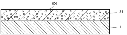
- a negative photosensitive resin composition is applied to one entire main surface of the substrate 1 to form a coating film 21.
- the ink repellent agent (D) is totally dissolved and uniformly dispersed in the coating film 21.
- the ink repellent agent (D) may be a hydrolyzable silane compound mixture (M) containing the hydrolyzable silane compound (s1) or a partially hydrolyzed (co) condensate thereof.
- the ink repellent agent (D) is schematically shown, and does not actually exist in such a particle shape.
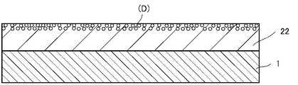
- the coating film 21 is dried to form a dry film 22.
- the drying method include heat drying, reduced pressure drying, and reduced pressure heat drying.
- the heating temperature is preferably 50 to 120 ° C, more preferably 90 to 115 ° C.
- the ink repellent agent (D) moves to the upper layer of the dry film.
- the upper surface transfer of an ink repellent agent (D) is similarly achieved within a coating film.
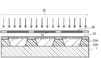
- the dry film 22 is irradiated with actinic rays and exposed through a photomask 30 having a masking portion 31 having a shape corresponding to the opening surrounded by the partition walls.
- the film after the dry film 22 is exposed is referred to as an exposure film 23.
- the exposed portion 23 ⁇ / b> A is photocured, and the non-exposed portion 23 ⁇ / b> B is in the same state as the dry film 22.
- the exposure is performed when the dry film 22 absorbs actinic rays and the photoacid generator (C) is decomposed to generate an acid. Due to the generated acid, a reaction in which the alkali-soluble resin (A) and the crosslinking agent (B) are combined proceeds, and a curing reaction by hydrolysis condensation of the ink repellent agent (D) proceeds.
- excimer laser such as visible light; ultraviolet light; far ultraviolet light; KrF excimer laser light, ArF excimer laser light, F 2 excimer laser light, Kr 2 excimer laser light, KrAr excimer laser light, and Ar 2 excimer laser light.
- Examples include light; X-ray; electron beam.
- the light to be irradiated is preferably light having a wavelength of 100 to 600 nm, more preferably light having a wavelength of 300 to 500 nm, and particularly preferably light containing i-line (365 nm), h-line (405 nm), or g-line (436 nm). Moreover, you may cut light below 330 nm as needed.
- the exposure method includes full-surface batch exposure, scan exposure, and the like. You may expose in multiple times with respect to the same location. At this time, the multiple exposure conditions may or may not be the same.
- Exposure amount In any of the above exposure method, for example, preferably 5 ⁇ 1,000mJ / cm 2, more preferably 5 ⁇ 500mJ / cm 2, more preferably 5 ⁇ 300mJ / cm 2, 5 ⁇ 200mJ / cm 2 is particularly preferable, and 5 to 50 mJ / cm 2 is most preferable.
- the exposure amount is appropriately optimized depending on the wavelength of light to be irradiated, the composition of the negative photosensitive resin composition, the thickness of the coating film, and the like.
- the negative photosensitive resin composition of the present invention can be sufficiently cured with such a low exposure amount.
- the exposure time per unit area is not particularly limited, and is designed from the exposure power of the exposure apparatus to be used, the required exposure amount, and the like. In the case of scan exposure, the exposure time is determined from the light scanning speed.
- the exposure time per unit area is usually about 1 to 60 seconds, preferably 1 to 30 seconds.
- heating may be performed for the purpose of diffusing the acid generated by the decomposition of the photoacid generator (C) into the dry film 22 and performing the reaction uniformly in the film.
- the heating conditions are 70 to 120 ° C., preferably 90 to 115 ° C., about 1 to 5 minutes, preferably 1 to 3 minutes.
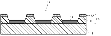
- FIG. 1D shows a state after the non-exposed portion 23B is removed by development.
- the non-exposed portion 23B is dissolved by an alkali developer in a state where the ink repellent agent (D) moves to the upper layer portion and the ink repellent agent (D) is hardly present in the lower layer. Therefore, the ink repellent agent (D) hardly remains in the opening 5.
- the uppermost layer including the upper surface is the ink repellent layer 4A.
- the ink repellent agent (D) present at a high concentration in the uppermost layer is cured using the acid generated by the photoacid generator (C) as a catalyst to form an ink repellent layer.
- the alkali-soluble resin (A) and the crosslinking agent (B) present around the ink repellent agent (D) and other photo-curing components are also strongly photocured, and the ink repellent agent (D ) And the ink repellent layer.
- the ink repellent agent (D) contains the hydrolyzable silane compound (s4)
- the ink repellent agent (D) is bonded to each other, and at the same time, the alkali-soluble resin (A) and the crosslinking agent (B), and the others
- the ink repellent layer 4A in which the ink repellent agent (D) is firmly bonded is formed by photocuring with the photocuring component.
- the alkali-soluble resin (A), the crosslinking agent (B), and other photo-curing components are photocured mainly on the lower side of the ink-repellent layer 4A.
- a layer 4B containing almost no is formed.
- the ink repellent agent (D) is sufficiently fixed to the partition including the ink repellent layer 4A and the lower layer 4B, and therefore hardly migrates to the opening during development.
- the partition 4 may be further heated.
- the heating temperature is preferably 130 to 250 ° C., more preferably 150 to 230 ° C., and the heating time is about 20 to 60 minutes, preferably 30 to 60 minutes.
- the partition 4 is hardened and the ink repellent agent (D) is more firmly fixed in the ink repellent layer 4A.
- the thus obtained cured resin film and partition 4 of the present invention have good ink repellency on the upper surface even when exposure is performed at a low exposure amount.
- the ink repellent (D) hardly exists in the opening 5 after development, and the uniform coating property of the ink in the opening 5 can be sufficiently ensured.
- the partition wall is used to remove a development residue or the like of the negative photosensitive resin composition that may be present in the opening 5 after heating.
- the substrate 1 with 4 may be subjected to ultraviolet / ozone treatment.
- the ink repellent layer above the partition obtained using the negative photosensitive resin composition of the present invention has sufficient resistance to ultraviolet / ozone treatment.
- the partition formed from the negative photosensitive resin composition of the present invention preferably has a width of, for example, 100 ⁇ m or less, and particularly preferably 20 ⁇ m or less. Usually, the width is preferably 5 ⁇ m or more.
- the distance between adjacent partition walls is preferably 300 ⁇ m or less, and particularly preferably 100 ⁇ m or less. Usually, the distance between adjacent barrier ribs (pattern width) is preferably 10 ⁇ m or more.
- the height of the partition wall is preferably 0.05 to 50 ⁇ m, particularly preferably 0.2 to 10 ⁇ m.
- the barrier ribs of the present invention are particularly excellent as barrier ribs for organic EL elements because the edge portions when formed in the above width have few irregularities and are excellent in linearity, and such highly accurate pattern formation is possible. Useful.
- the partition of the present invention can be used as a partition having the opening as an ink injection region when pattern printing is performed by the IJ method (inkjet method).
- IJ method inkjet method
- the partition wall of the present invention is formed and used so that the opening thereof coincides with a desired ink injection region, the partition top surface has good ink repellency. It is possible to suppress ink from being injected into an undesired opening, that is, an ink injection region, beyond the partition wall.
- the opening surrounded by the partition wall has good ink wetting and spreading properties, it is possible to print the ink uniformly in a desired region without causing white spots or the like.
- the partition wall of the present invention has an optical element, particularly an organic EL element, a quantum dot display, a TFT array, etc., having a partition wall positioned between dots adjacent to a plurality of dots on the substrate surface on which dots are formed by the IJ method. It is useful as a partition wall.
- an organic EL element As an optical element of the embodiment of the present invention, an organic EL element, a quantum dot display, a TFT array, or a thin film solar cell having a plurality of dots and a partition wall of the present invention located between adjacent dots on the substrate surface can be mentioned.
- the dots are preferably formed by the IJ method.
- the organic EL element has a structure in which a light emitting layer of an organic thin film is sandwiched between an anode and a cathode, and the partition of the present invention is used for a partition that separates the organic light emitting layer, a partition that separates the organic TFT layer, and a coating type oxide semiconductor. It can be used for separating partition applications.
- the organic TFT array element is a semiconductor layer including a plurality of dots arranged in a matrix in plan view, each pixel having a pixel electrode and a TFT as a switching element for driving it, and including a TFT channel layer.
- the organic TFT array element is provided as a TFT array substrate in, for example, an organic EL element or a liquid crystal element.
- an organic EL element which is an optical element according to an embodiment of the present invention will be described below by using an IJ method to form dots in the opening using the partition obtained above.
- the formation method of the dot in the organic EL element etc. which are the optical elements of embodiment of this invention is not limited to the following.
- 2A and 2B schematically show a method for manufacturing an organic EL element using the partition walls 4 formed on the substrate 1 shown in FIG. 1D.
- the partition 4 on the substrate 1 is formed such that the opening 5 matches the dot pattern of the organic EL element to be manufactured.
- ink 10 is dropped from the inkjet head 9 into the opening 5 surrounded by the partition wall 4 and a predetermined amount of ink 10 is injected into the opening 5.
- known inks for organic EL elements are appropriately selected and used in accordance with the function of dots.
- an organic EL element, a quantum dot display, a TFT array, or a thin-film solar cell which is an optical element according to an embodiment of the present invention, is formed in the opening partitioned by the partition in the manufacturing process by using the partition of the present invention.
- Ink can be spread evenly and uniformly without unevenness, which makes it possible to have dots formed accurately.
- the organic EL element can be manufactured, for example, as follows, but is not limited thereto.
- a light-transmitting electrode such as tin-doped indium oxide (ITO) is formed on a light-transmitting substrate such as glass by a sputtering method or the like.
- the translucent electrode is patterned as necessary.
- partition walls are formed in a lattice shape in plan view along the outline of each dot by photolithography including coating, exposure and development.
- the materials of the hole injection layer, the hole transport layer, the light emitting layer, the hole blocking layer, and the electron injection layer are respectively applied and dried in the dots by the IJ method, and these layers are sequentially stacked. To do.
- the kind and number of organic layers formed in the dots are appropriately designed.
- a reflective electrode such as aluminum is formed by vapor deposition or the like.
- the quantum dot display can be manufactured in the same manner except that the light emitting layer is a quantum dot layer, but is not limited thereto.
- optical element of the embodiment of the present invention can be applied to, for example, a blue light conversion type quantum dot display manufactured as follows.
- a negative photosensitive resin composition of the present invention is used for a light-transmitting substrate such as glass, and partition walls are formed in a lattice shape in plan view along the outline of each dot.
- a nanoparticle solution that converts blue light into green light by the IJ method, a nanoparticle solution that converts blue light into red light, and a blue color ink as necessary are applied to the dots and dried.
- a liquid crystal display having excellent color reproducibility can be obtained by using a light source that emits blue as a backlight and using the module as a color filter alternative.
- the TFT array can be manufactured, for example, as follows, but is not limited thereto.
- a gate electrode such as aluminum or an alloy thereof is formed on a light-transmitting substrate such as glass by a sputtering method or the like. This gate electrode is patterned as necessary.
- a gate insulating film such as silicon nitride is formed by a plasma CVD method or the like.
- a source electrode and a drain electrode may be formed over the gate insulating film.
- the source electrode and the drain electrode can be manufactured by forming a metal thin film such as aluminum, gold, silver, copper, or an alloy thereof by, for example, vacuum deposition or sputtering.
- a resist is applied, exposed and developed, and the resist is left in a portion where the electrode is to be formed, and then phosphoric acid or aqua regia is used. There is a technique of removing the exposed metal and finally removing the resist.
- the source electrode and the drain electrode may be formed using a metal nanocolloid such as silver or copper by a method such as an inkjet method.
- partition walls are formed in a lattice pattern in plan view along the outline of each dot by photolithography including coating, exposure and development.
- a semiconductor solution is applied in the dots by the IJ method, and the solution is dried to form a semiconductor layer.
- an organic semiconductor solution, an inorganic coating type oxide semiconductor solution, or the like can also be used.
- the source electrode and the drain electrode may be formed using a method such as an ink jet method after the semiconductor layer is formed.
- a transparent electrode such as ITO is formed by sputtering or the like, and a protective film such as silicon nitride is formed.
- Examples 1, 2, and 3 are examples, and example 4 is a comparative example.
- the sample was diluted to 1.0% by mass with tetrahydrofuran and passed through a 0.5 ⁇ m filter, and then the GPC of the sample was measured using the GPC measurement apparatus.
- the number average molecular weight (Mn) of the sample was determined by computer analysis of the GPC spectrum of the sample using the calibration curve.
- PGMEA a liquid which is a PGMEA solution containing 10% by mass of an ink repellent agent (Dcf).
- the obtained fluorine-containing content (mass% of fluorine atoms) of the composition excluding the solvent of the (Dcf-1) solution is 27.4 mass%.
- the composition excluding the solvent in the (Dcf-1) solution had a number average molecular weight (Mn) of 49,325.
- the fluorine atom content and the number average molecular weight (Mn) of the ink repellent agent (D) are the same as the charged amount composition (mol%) of the ink repellent agent (D). In addition, it is shown in Table 1 together.
- Example 1 (Preparation of negative photosensitive resin composition) 0.967 g of liquid (D1-1) (solid content is 0.097 g, the rest is PGME (solvent)), 19.34 g of EP4020G, 4.84 g of MW-100LM, 0.73 g of CPI-210S, and PGMEA was put in a stirring vessel of 500 cm 3 and stirred for 30 minutes to prepare a negative photosensitive resin composition 1.
- a drying treatment is performed on a hot plate at a temperature of 100 ° C. for 2 minutes to obtain a film thickness of 2.5 ⁇ m.
- a dry film was formed.
- a gap of 50 ⁇ m is formed on the surface of the obtained dry film from the film side through a photomask having a hole pattern (2.5 cm ⁇ 5 cm) (a photomask that is irradiated with light other than the pattern area). Open and irradiated with ultraviolet light from a high pressure mercury lamp at 25 mW / cm 2 for 1 second, 2 seconds, 5 seconds or 10 seconds.
- the exposed glass substrate was developed by immersing it in a 2.38 mass% tetramethylammonium hydroxide aqueous solution for 40 seconds, and the dry film of the unexposed part was washed away with water and dried. Next, by heating this on a hot plate at 230 ° C. for 50 minutes, four types of glass in which a cured film (partition) of the negative photosensitive resin composition 1 was formed in a region excluding the hole pattern portion. A substrate (1) was obtained.
- the entire surface on which the cured film was formed was irradiated with ultraviolet rays / ozone for 1 minute.
- the contact angle to PGMEA on the surface of the cured film (partition) after irradiation for 1 minute and the contact angle to water on the glass substrate surface were measured.
- the measurement method is the same as described above.
- ⁇ Storage stability> The negative photosensitive resin composition was stored in a glass screw bottle at 23 ° C. (room temperature) for one month. After storage for one month, a negative photosensitive resin composition is applied to the surface of a 10 cm ⁇ 10 cm glass substrate that has been cleaned in the same manner as in the production of the above cured film (partition wall) using a spinner to form a coating film did. Furthermore, it was dried on a hot plate at 100 ° C. for 2 minutes to form a dry film having a thickness of 2 ⁇ m. The appearance of the dried film was visually observed and evaluated according to the following criteria.
- Negative photosensitive resin composition 2 and a cured film of negative photosensitive resin composition 2 were formed in the same manner as in Example 1 except that (D2-1) liquid was used instead of (D1-1) liquid.
- a glass substrate (2) was prepared and evaluated in the same manner as in Example 1.
- Example 3 The negative photosensitive resin composition 3 and a cured film of the negative photosensitive resin composition 3 were formed in the same manner as in Example 1 except that the (D3-1) liquid was used instead of the (D1-1) liquid.
- a glass substrate (3) was prepared and evaluated in the same manner as in Example 1.
- Example 4 The negative photosensitive resin composition 4 and the cured film of the negative photosensitive resin composition 4 were formed in the same manner as in Example 1 except that the (Dcf-1) liquid was used instead of the (D1-1) liquid.
- a glass substrate (4) was prepared and evaluated in the same manner as in Example 1. The evaluation results of Examples 2 to 4 are shown in Table 2 together with the composition of the negative photosensitive resin composition.
- Example 2 From Table 2, the cured films obtained in Examples 1, 2 and 3 used the ink repellent agent of the present invention, and therefore showed good ink repellency even after low exposure, and after UV / ozone irradiation. It can be seen that high ink repellency is maintained and the glass substrate surface has good hydrophilicity. Moreover, it turns out that storage stability is also high. On the other hand, in Example 4, since the ink repellent agent not according to the present invention was used, it was found that high ink repellency could not be maintained after ultraviolet / ozone irradiation.
- the partition formed using the negative photosensitive resin composition of the present invention has good ink repellency and can retain ink repellency even after ultraviolet / ozone irradiation, and the openings partitioned by the partition It is useful for optical elements having dots that are uniformly coated with ink and formed with high precision.
- the negative photosensitive resin composition of the present invention can be used for various optical elements, particularly organic layers such as a light emitting layer of organic EL elements, quantum dot layers and hole transport layers of quantum dot displays, and conductors of TFT arrays Composition for forming barrier ribs for pattern printing by the IJ method in patterns, semiconductor patterns, organic semiconductor layers forming TFT channel layers, gate electrodes, source electrodes, drain electrodes, gate wirings and source wirings, thin film solar cells, etc. It can be suitably used as a product.
- organic layers such as a light emitting layer of organic EL elements, quantum dot layers and hole transport layers of quantum dot displays, and conductors of TFT arrays Composition for forming barrier ribs for pattern printing by the IJ method in patterns, semiconductor patterns, organic semiconductor layers forming TFT channel layers, gate electrodes, source electrodes, drain electrodes, gate wirings and source wirings, thin film solar cells, etc. It can be suitably used as a product.
Landscapes
- Physics & Mathematics (AREA)
- General Physics & Mathematics (AREA)
- Optics & Photonics (AREA)
- Nonlinear Science (AREA)
- Spectroscopy & Molecular Physics (AREA)
- Crystallography & Structural Chemistry (AREA)
- Chemical & Material Sciences (AREA)
- Mathematical Physics (AREA)
- Materials For Photolithography (AREA)
- Electroluminescent Light Sources (AREA)
- Life Sciences & Earth Sciences (AREA)
- Engineering & Computer Science (AREA)
- Sustainable Development (AREA)
- Sustainable Energy (AREA)
- Photovoltaic Devices (AREA)
Abstract
Description
本発明は、上記観点からなされたものであって、隔壁上面に低露光量で充分な撥インク性を有する撥インク層の形成が可能であり、かつ該撥インク層が親インク化処理を経ても、優れた撥インク性を持続できる隔壁の製造に使用可能なネガ型感光性樹脂組成物を提供することを課題とする。
本発明は、上面に充分な撥インク性を有する撥インク層を有し、微細で精度の高いパターンの形成が可能な隔壁であり、親インク化処理を経ても、優れた撥インク性を持続できる光学素子の隔壁を提供することを課題とする。
また、本発明は、隔壁で仕切られた開口部にインクが均一に塗布され、精度よく形成されたドットを有する光学素子、具体的には、有機EL素子、量子ドットディスプレイ、TFTアレイまたは薄膜太陽電池の提供を目的とする。
[1]アルカリ可溶性樹脂(A)と、架橋剤(B)と、光酸発生剤(C)と、フルオロアルキレン基および/またはフルオロアルキル基と加水分解性基とを有する加水分解性シラン化合物(s1)を単量体および/または部分加水分解(共)縮合物として含む撥インク剤(D)と、を含むネガ型感光性樹脂組成物。
[2]前記撥インク剤(D)中のフッ素原子の含有率が1~40質量%である、上記[1]に記載のネガ型感光性樹脂組成物。
[3]前記撥インク剤(D)は、ケイ素原子に4個の加水分解性基が結合した加水分解性シラン化合物(s2)を単量体および/または部分加水分解(共)縮合物として含む、上記[1]または[2]に記載のネガ型感光性樹脂組成物。
[4]前記撥インク剤(D)は、炭化水素基と加水分解性基のみを有する加水分解性シラン化合物(s3)を単量体および/または部分加水分解(共)縮合物として含む、上記[1]~[3]のいずれかに記載のネガ型感光性樹脂組成物。
[5]前記撥インク剤(D)は、カチオン重合性基と加水分解性基とを有しフッ素原子を含まない加水分解性シラン化合物(s4)を単量体および/または部分加水分解(共)縮合物として含む、上記[1]~[4]のいずれかに記載のネガ型感光性樹脂組成物。
[6]前記アルカリ可溶性樹脂(A)の含有量が、ネガ型感光性樹脂組成物における全固形分中、10~90質量%である、上記[1]~[5]のいずれか1項に記載のネガ型感光性樹脂組成物。
[7]前記架橋剤(B)、および光酸発生剤の含有量が、アルカリ可溶性樹脂(A)の100質量部に対して、それぞれ2~50質量部、および0.1~20質量部である、上記[1]~[6]のいずれか1項に記載のネガ型感光性樹脂組成物。
[8]前記撥インク剤(D)の含有量が、アルカリ可溶性樹脂(A)の100質量部に対して0.01~20質量部である、上記[1]~[7]のいずれか1項に記載のネガ型感光性樹脂組成物。
[9]さらに、プロピレングリコールモノメチルエーテルアセテート、プロピレングリコールモノメチルエーテル、ジエチレングリコールエチルメチルエーテル、ジエチレングリコールモノエチルエーテルアセテートおよび2-プロパノールからなる群から選ばれる少なくとも1種の溶媒(E)を含む、上記[1]~[8]のいずれか1項に記載のネガ型感光性樹脂組成物。
[11]基板表面をドット形成用の複数の区画に仕切る形に形成された隔壁であって、上記[1]~[10]のいずれかに記載のネガ型感光性樹脂組成物の硬化膜からなる隔壁。
[12]幅が100μm以下であり、隔壁間の距離(パターンの幅)が300μm以下であり、高さが0.05~50μmである、上記[11]に記載の隔壁。
[13]基板表面に複数のドットと、隣接するドット間に位置する隔壁とを有する光学素子であって、前記隔壁が上記[11]または[12]に記載の隔壁で形成されていることを特徴とする光学素子。
[14]前記ドットがインクジェット法で形成されている、上記[13]に記載の光学素子。
[15]前記光学素子が、有機EL素子、量子ドットディスプレイ、TFTアレイまたは薄膜太陽電池である、上記[13]または[14]に記載の光学素子。
また、本発明の隔壁は、上面に充分な撥インク性を有する撥インク層を有し、微細で精度の高いパターンの形成が可能であり、当該隔壁で仕切られた、開口部にインクが均一に塗布され、精度よく形成されたドットを有する光学素子を用いてなる、有機EL素子、量子ドットディスプレイ、TFTアレイまたは薄膜太陽電池が提供できる。
「(メタ)アクリロイル基」は、「メタクリロイル基」と「アクリロイル基」の総称である。(メタ)アクリロイルオキシ基、(メタ)アクリル酸、(メタ)アクリレート、(メタ)アクリルアミド、および(メタ)アクリル樹脂もこれに準じる。
式(y)で表される化合物を、単に化合物(y)と記載することがある。
ここで、式(x)および式(y)は、任意の式を示している。
感光性樹脂組成物を塗布した膜を「塗膜」、それを乾燥させた膜を「乾燥膜」という。該「乾燥膜」を硬化させて得られる膜は「樹脂硬化膜」である。また、「樹脂硬化膜」を単に「硬化膜」ということもある。
有機EL素子、液晶素子のカラーフィルタおよびTFT(Thin Film Transistor)アレイ等の光学素子においては、各種構成要素としてのドットを、該ドット形成用のインクを用いてインクジェット(IJ)法によりパターン印刷することがある。「インク」には、かかる用途に用いられるインクが含まれる。
本発明のネガ型感光性樹脂組成物は、アルカリ可溶性樹脂(A)と、架橋剤(B)と、光酸発生剤(C)と、フルオロアルキレン基および/またはフルオロアルキル基と加水分解性基とを有する加水分解性シラン化合物(s1)を単量体および/または部分加水分解(共)縮合物として含む撥インク剤(D)と、を含有する。
本発明のネガ型感光性樹脂組成物は、さらに必要に応じて、溶媒(E)、その他の任意成分を含有する。
本発明のネガ型感光性樹脂組成物におけるアルカリ可溶性樹脂(A)としては、活性光線の照射(露光)により光酸発生剤(C)が発生する酸の作用によって、架橋剤(B)と結合し、架橋されてアルカリ不溶となるカチオン重合型のアルカリ可溶性樹脂(A)であれば、特に制限なく、使用可能である。
ポリビニルフェノールは、4-ビニルフェノール、3-ビニルフェノール、2-ビニルフェノール、2-メチル-4-ビニルフェノール、2,6-ジメチル-4-ビニルフェノール等のビニルフェノールを単独または、2種以上組み合わせて、アゾビスイソブチロニトリル、ベンゾイルパーオキサイド等の重合開始剤を用いて、ラジカル重合させることによって得ることができる。
ネガ型感光性樹脂組成物における全固形分中のアルカリ可溶性樹脂(A)の含有量は、10~90質量%が好ましく、30~85質量%がより好ましく、40~80質量%が特に好ましい。含有量が上記範囲であると、ネガ型感光性樹脂組成物の現像性が良好になる。
架橋剤(B)は、活性光線の照射(露光)により、光酸発生剤(C)が発生する酸の作用によって、上記アルカリ可溶性樹脂(A)と結合して、アルカリ可溶性樹脂(A)を架橋させることでアルカリ不溶としうる化合物(感酸物質)である。
ベンゾグアナミン系化合物としては、例えば、ベンゾグアナミン、メチル化ベンゾグアナミンなどが挙げられる。
尿素系化合物としては、例えば、尿素、モノメチロール尿素、ジメチロール尿素、アルコキシメチレン尿素、N-アルコキシメチレン尿素、エチレン尿素、エチレン尿素カルボン酸、テトラキス(メトキシメチル)グリコールウリルなどが挙げられる。 イソシアネート系化合物としては、例えば、ヘキサメチレンジイソシアネート、1,4-シクロヘキシルジイソシアネート、トルエンジイソシアネート、ビスイソシアネートメチルシクロヘキサン、ビスイソシアネートメチルベンゼン、エチレンジイソシアネートなどが挙げられる。
光酸発生剤(C)は、活性光線を照射することで、分解して酸を発生する化合物であれば、特に制限されない。カチオン重合型のアルカリ可溶性樹脂(A)を用いた感光性樹脂組成物において、一般に光酸発生剤として用いられる化合物の中から、任意の化合物を選択して使用することができる。

なお、これらのオニウム塩においては、カチオン部が照射された光を吸収し、アニオン部が酸の発生源となる。
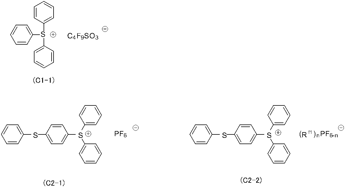
なお、化合物(C3)、(C4)、(C6)、および(C7)においては、各化合物の骨格を形成するベンゼン環の水素原子が置換された化合物も光酸発生剤としての機能を有する。
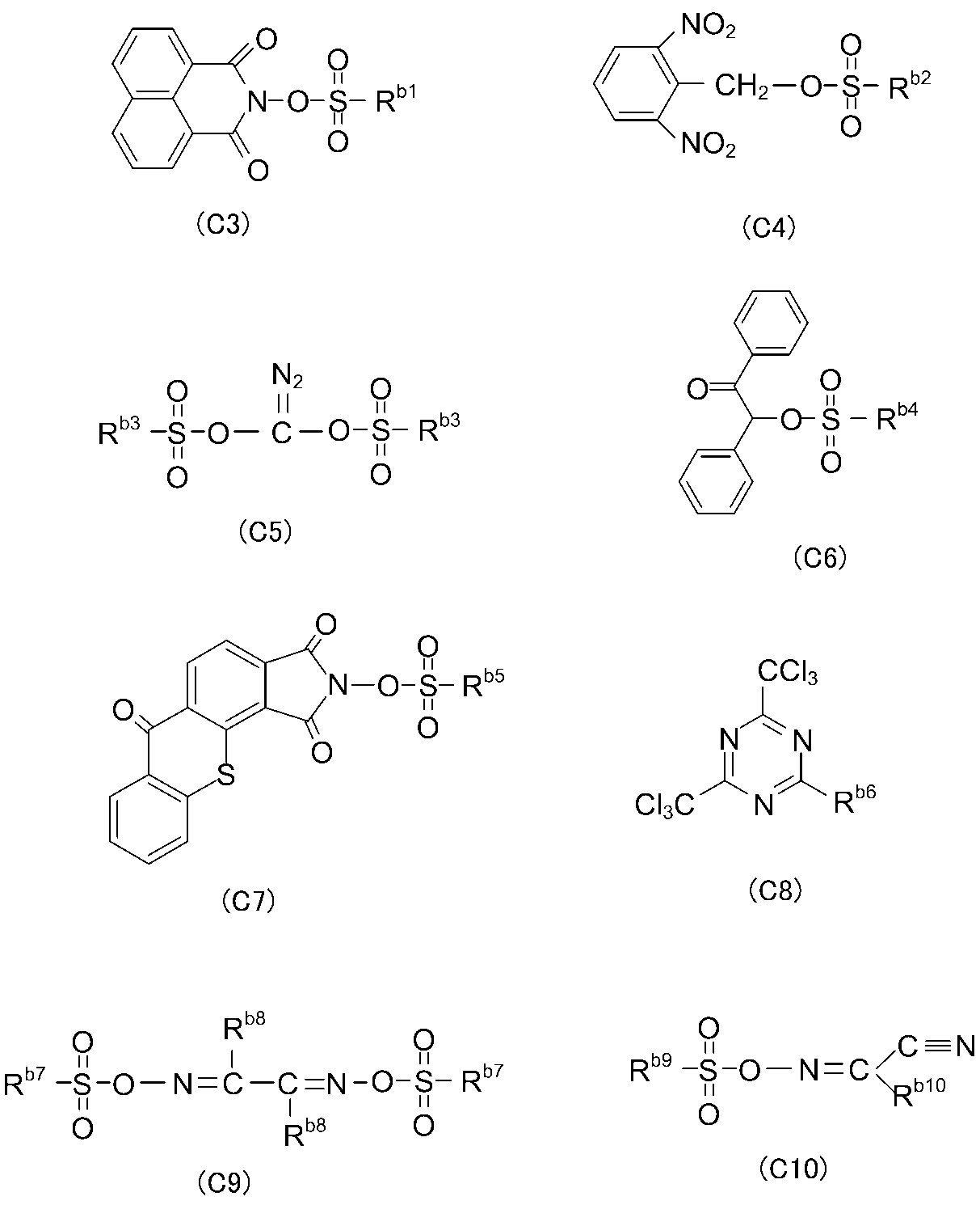
なお、これらの非イオン系光酸発生剤においては、塩素原子、アルカンスルホン酸、アリールスルホン酸等が結合した部分が酸の発生源となる。
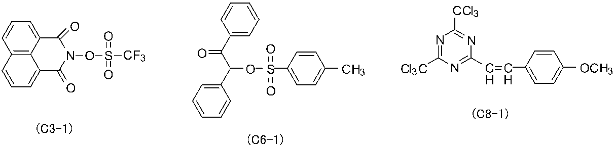
光酸発生剤(C)の含有量は、アルカリ可溶性樹脂(A)の100質量部に対して0.1~20質量部が好ましく、0.5~10質量部がより好ましく、1~8質量部が特に好ましい。光酸発生剤(C)の含有量を上記範囲とすることで、上面に充分な撥インク性を有する、微細で精度の高いパターンの形成が可能な隔壁が得られる。
本発明における撥インク剤(D)は、フルオロアルキレン基および/またはフルオロアルキル基と加水分解性基とを有する加水分解性シラン化合物(s1)を含有する。撥インク剤(D)は、加水分解性シラン化合物(s1)を単独でも、加水分解性シラン化合物(s1)と、後述する任意成分としての、加水分解性シラン化合物(s1)以外の加水分解性シラン化合物との混合物としてもよい。撥インク剤(D)は、加水分解性シラン化合物(s1)を含む加水分解性シラン化合物のみで構成されることが好ましい。
加水分解性シラン化合物(s3);ケイ素原子に結合する基として、炭化水素基と加水分解性基のみを有する加水分解性シラン化合物。
加水分解性シラン化合物(s4);カチオン重合性基と加水分解性基とを有し、フッ素原子を含まない加水分解性シラン化合物。
以下、加水分解性シラン化合物(s1)~(s4)、およびその他の加水分解性シラン化合物について説明する。
加水分解性シラン化合物(s1)を用いることで、撥インク剤(D)はフッ素原子をフルオロアルキレン基および/またはフルオロアルキル基の形で有し、優れた上面移行性と撥インク性を有する。加水分解性シラン化合物(s1)が有するこれらの性質をより高いレベルとするためには、加水分解性シラン化合物(s1)は、フルオロアルキル基、ペルフルオロアルキレン基およびペルフルオロアルキル基からなる群から選ばれる少なくとも1種を有することがより好ましく、ペルフルオロアルキル基を有することが特に好ましい。また、エーテル性酸素原子を含むペルフルオロアルキル基も好ましい。すなわち、加水分解性シラン化合物(s1)として最も好ましい化合物は、ペルフルオロアルキル基および/またはエーテル性酸素原子を含むペルフルオロアルキル基を有する化合物である。
加水分解性シラン化合物(s1)は、1種を単独で用いても、2種以上を併用してもよい。
(A-RF11)a-Si(RH11)bX11 (4-a-b) …(dx-1)
式(dx-1)中、RF11は、少なくとも1つのフルオロアルキレン基を含む、エーテル性酸素原子を含んでいてもよい炭素原子数1~16の2価の有機基である。
RH11は炭素原子数1~6の炭化水素基である。
aは1または2、bは0または1、a+bは1または2である。
Aはフッ素原子または下式(Ia)で表される基である。
-Si(RH12)cX12 (3-c) …(Ia)
RH12は炭素原子数1~6の炭化水素基である。
cは0または1である。
X11およびX12は、それぞれ独立に、加水分解性基である。
X11が複数個存在する場合、これらは互いに異なっていても同一であってもよい。
X12が複数個存在する場合、これらは互いに異なっていても同一であってもよい。
A-RF11が複数個存在する場合、これらは互いに異なっていても同一であってもよい。
式(dx-1)中、aが1であり、bが0または1であることが特に好ましい。
X11およびX12の具体例および好ましい様態は上記のとおりである。
T-RF12-Q11-SiX11 3 …(dx-1a)
式(dx-1a)中、RF12は炭素原子数2~15のエーテル性酸素原子を含んでいてもよいペルフルオロアルキレン基である。
Tはフッ素原子または下式(Ib)で表される基である。
-Q12-SiX12 3 …(Ib)
X11およびX12は、それぞれ独立に、加水分解性基である。
3個のX11は互いに異なっていても同一であってもよい。
3個のX12は互いに異なっていても同一であってもよい。
Q11およびQ12は、それぞれ独立に、炭素原子数1~10のフッ素原子を含まない2価の有機基を示す。
また、式(dx-1a)において、Tが基(Ib)である場合、RF12は、炭素原子数3~15のペルフルオロアルキレン基、または炭素原子数3~15のエーテル性酸素原子を含むペルフルオロアルキレン基が好ましく、炭素原子数4~6のペルフルオロアルキレン基が特に好ましい。
RF12がエーテル性酸素原子を含むペルフルオロアルキル基である場合、Q11およびQ12としては、-(CH2)i1-、-CH2O(CH2)i2-、-SO2NR1-(CH2)i3-、または-(C=O)-NR1-(CH2)i4-で表される基が好ましい。この場合においても、Q11およびQ12としては、-(CH2)i1-がより好ましい。i1は2~4の整数がさらに好ましく、i1は2が特に好ましい。
ケイ素原子に4個の加水分解性基が結合した加水分解性シラン化合物(s2)を混合物(M)に含ませることで、撥インク剤(D)を含むネガ型感光性樹脂組成物を硬化してなる硬化膜において、撥インク剤(D)が上面移行した後の造膜性を高められる。すなわち、加水分解性シラン化合物(s2)中の加水分解性基の数が多いことから、上面移行した後に、撥インク剤(D)同士が良好に縮合し、上面全体に薄い膜を形成して撥インク層となると考えられる。
また、混合物(M)に加水分解性シラン化合物(s2)を含ませることで、部分加水分解縮合物とした場合には、撥インク剤(D)は炭化水素系の溶媒に溶解しやすくなる。
加水分解性シラン化合物(s2)は、1種を単独で用いても、2種以上を併用してもよい。
SiX2 4 …(dx-2)
式(dx-2)中、X2は加水分解性基を示し、4個のX2は互いに異なっていても同一であってもよい。X2としては、前記X11およびX12と同様の基が用いられる。
Si(OCH3)4、Si(OC2H5)4、Si(OCH3)4の部分加水分解縮合物、またはSi(OC2H5)4の部分加水分解縮合物。
上記混合物(M)において、加水分解性シラン化合物(s2)を用いる場合、例えば、感光性樹脂組成物を硬化してなる隔壁において、その上面の端部に盛り上がりが形成される場合がある。この盛り上がりは、走査型電子顕微鏡(SEM)等によって観察されるレベルの微小なものであるが、他の部分よりもFおよび/またはSiの含有量が多いことが確認された。
加水分解性基の数の多い加水分解性シラン化合物(s2)によって生成されるシラノール基同士の反応により、撥インク剤(D)の造膜性は増加するが、その高い反応性のために、上記盛り上がりが起こると考えられる。そこで、加水分解性シラン化合物(s2)の一部を、加水分解性基の数の少ない加水分解性シラン化合物(s3)に置き換えることで、シラノール基同士の反応が抑えられ、上記盛り上がりの発生が抑えられると考えられる。
加水分解性シラン化合物(s3)は、1種を単独で用いても、2種以上を併用してもよい。
加水分解性基としては、加水分解性シラン化合物(s1)の加水分解性基と同様のものを用いることができる。
(RH5)j-SiX5 (4-j) …(dx-3)
式(dx-3)中、RH5は炭素原子数1~20の炭化水素基である。
X5は加水分解性基である。
jは1~3の整数であり、好ましくは2または3である。
RH5が複数個存在する場合、これらは互いに異なっていても同一であってもよい。
X5が複数個存在する場合、これらは互いに異なっていても同一であってもよい。
X5としては、前記X11およびX12と同様の基が用いられる。
混合物(M)は、任意に、カチオン重合性基と加水分解性基とを有し、フッ素原子を含有しない加水分解性シラン化合物(s4)を含有することが好ましい。混合物(M)に加水分解性シラン化合物(s4)を含ませることで、カチオン重合性基を介して、例えば、感光性樹脂組成物が含有する架橋剤(B)と反応して、撥インク層における撥インク剤(D)の定着性を高める効果が得られる。
(E-Q6)s-Si(RH6)tX6 (4-s-t) …(dx-4)
式(dx-4)中、Eはカチオン重合性基、例えば、オキセタニル基、エポキシ基、グリシドキシ基または3,4-エポキシシクロヘキシル基である。
Q6は炭素原子数1~10のフッ素原子を含まない2価の有機基である。
RH6は炭素原子数1~6の炭化水素基である。
X6は加水分解性基である。
sは1または2、tは0または1、s+tは1または2である。
E-Q6が複数個存在する場合、これらは互いに異なっていても同一であってもよい。
X6が複数個存在する場合、これらは互いに異なっていても同一であってもよい。
Q6としては、炭素原子数1~10のアルキレン基が好ましく、炭素原子数1~5のアルキレン基がより好ましく、炭素原子数1~3のアルキレン基が特に好ましい。
RH6としては、前記RH11およびRH12と同様の基が用いられる。
混合物(M)は、さらに加水分解性シラン化合物(s1)~(s4)以外の加水分解性シラン化合物の1種または2種以上を、本発明の効果を損なわない範囲で含むことができる。混合物(M)におけるその他の加水分解性シラン化合物の含有量は、混合物(M)の全量に対して合計で40モル%以下が好ましく、10モル%以下がより好ましい。
イソシアネート基と加水分解性基とを有し、フッ素原子を含まない加水分解性シラン化合物としては、例えば、NCO(CH2)3Si(OC2H5)3(イソシアネートプロピルトリエトキシシラン)等が挙げられる。
撥インク剤(D)は、混合物(M)またはその部分加水分解(共)縮合物である。
撥インク剤(D)の一例として、化合物(dx-1a)を必須成分として含み、化合物(dx-2)および化合物(dx-4)を任意成分として含み、化合物(dx-1a)中の基Tがフッ素原子である混合物(M)が挙げられる。各化合物の含有量は上記のとおりが好ましい。
式(II)中、n1~n3は構成単位の合計モル量に対する各構成単位のモル分率を示す。n1>0、n2≧0、n3≧0、n1+n2+n3=1である。その他の各符号は、上述のとおりである。ただし、Tはフッ素原子である。
式(II)で表される平均組成式は、撥インク剤(D1)において、加水分解性基またはシラノール基の全てがシロキサン結合となったと仮定した場合の化学式である。
また、式(II)において、化合物(dx-1a)、(dx-2)、および(dx-3)にそれぞれ由来する単位は、ランダムに配列していると推測される。
各成分のモル比は、各成分の効果のバランスから設計されることが好ましい。
n1は、撥インク剤(D1)におけるフッ素原子の含有率が、上記好ましい範囲となる量において、0.02~0.4が好ましく、0.02~0.3が特に好ましい。
n2は、n3=0の場合は0~0.98が好ましく、n3>0の場合は0.05~0.6が好ましい。
n3は、0~0.5が好ましい。
なお、上記各成分の好ましいモル比は、化合物(dx-1a)中のTが基(Ib)である場合も同様である。
数平均分子量(Mn)が上記下限値以上であると、感光性樹脂組成物を用いて隔壁を形成する際に、撥インク剤(D)が上面移行しやすい。上記上限値未満であると、撥インク剤(D)の溶媒への溶解性が良好になる。
撥インク剤(D)の数平均分子量(Mn)は、製造条件により調節できる。
上記反応には、通常用いられる塩酸、硫酸、硝酸、リン酸等の無機酸、あるいは、酢酸、シュウ酸、マレイン酸等の有機酸を触媒として用いることが好ましい。また、必要に応じて、水酸化ナトリウム、水酸化テトラメチルアンモニウム(TMAH)等のアルカリ触媒を用いてもよい。
上記反応には公知の溶媒を用いることができる。
上記反応で得られる撥インク剤(D)は、溶媒とともに、溶液の性状で感光性樹脂組成物に配合してもよい。
撥インク剤(D)の含有量は、アルカリ可溶性樹脂(A)の100質量部に対して0.01~20質量部が好ましく、0.1~10質量部がより好ましく、0.2~3質量部が特に好ましい。撥インク剤(D)の含有量を上記範囲とすることで、上面に充分な撥インク性を有する隔壁が得られる。
本発明のネガ型感光性樹脂組成物は、溶媒(E)を含有することで粘度が低減され、ネガ型感光性樹脂組成物の基材表面への塗布がしやすくなる。その結果、均一な膜厚のネガ型感光性樹脂組成物の塗膜が形成できる。
溶媒(E)としては公知の溶媒が用いられる。溶媒(E)は、1種を単独で用いても、2種以上を併用してもよい。
本発明におけるネガ型感光性樹脂組成物は、さらに、必要に応じて、着色剤、熱架橋剤、高分子分散剤、分散助剤、シランカップリング剤、微粒子、硬化促進剤、増粘剤、可塑剤、消泡剤、レベリング剤、ハジキ防止剤等の他の添加剤を1種または2種以上含有してもよい。
また、本発明のネガ型感光性樹脂組成物を用いれば、低露光量で、上面に良好な撥インク性を有する撥インク層を有する隔壁の製造が可能である。さらに、該撥インク層が、紫外線/オゾン洗浄処理等の親インク化処理を経ても、優れた撥インク性を持続できる隔壁の製造が可能である。
本発明により製造できる隔壁は、上面に充分な撥インク性を有する撥インク層を有し、微細で精度の高いパターンの形成が可能である。
本発明によれば、隔壁で仕切られた開口部に、インクが均一に塗布され精度よく形成されたドットを有する光学素子、具体的には、有機EL素子、量子ドットディスプレイ、TFTアレイ、薄膜太陽電池等が提供できる。
本発明の隔壁は、基板表面をドット形成用の複数の区画に仕切る形に形成された、上記のネガ型感光性樹脂組成物の硬化物からなる。該隔壁は、例えば、基板等の基材の表面に、本発明のネガ型感光性樹脂組成物を塗布し、必要に応じて、乾燥して溶媒等を除去した後、ドット形成用の区画となる部分にマスキングを施し、露光した後、必要に応じて、加熱し、現像することで得られる。
この乾燥過程において、撥インク剤(D)は乾燥膜の上層部に移行する。なお、ネガ型感光性樹脂組成物が、溶媒(E)を含有しない場合であっても、塗膜内で撥インク剤(D)の上面移行は同様に達成される。
照射する光としては、波長100~600nmの光が好ましく、300~500nmの光がより好ましく、i線(365nm)、h線(405nm)またはg線(436nm)を含む光が特に好ましい。また、必要に応じて330nm以下の光をカットしてもよい。
単位面積当たりの露光時間は、通常1~60秒間程度、好ましくは1~30秒である。
このようにして、撥インク剤(D)は、撥インク層4Aおよび下部層4Bを含む隔壁に充分に定着しているため、現像時に開口部にマイグレートすることがほとんどない。
加熱により、隔壁4の硬化はより強固なものとなり、撥インク剤(D)は、撥インク層4A内により強固に定着する。
隔壁の高さは0.05~50μmであることが好ましく、0.2~10μmであることが特に好ましい。
本発明の実施形態の光学素子としては、基板表面に複数のドットと隣接するドット間に位置する本発明の隔壁とを有する、有機EL素子、量子ドットディスプレイ、TFTアレイまたは薄膜太陽電池が挙げられる。上記の有機EL素子、量子ドットディスプレイ、TFTアレイ、または薄膜太陽電池において、ドットはIJ法により形成されることが好ましい。
なお、本発明の実施形態の光学素子である有機EL素子等におけるドットの形成方法は、以下に限定されない。
図2Aおよび図2Bは、図1Dに示す基板1上に形成された隔壁4を用いて有機EL素子を製造する方法を模式的に示すものである。ここで、基板1上の隔壁4は、開口部5が、製造しようとする有機EL素子のドットのパターンに一致するように形成されたものである。
ガラス等の透光性基板にスズドープ酸化インジウム(ITO)等の透光性電極をスパッタ法等によって成膜する。この透光性電極は、必要に応じてパターニングされる。
次に、本発明のネガ型感光性樹脂組成物を用い、塗布、露光および現像を含むフォトリソグラフィ法により、各ドットの輪郭に沿って、平面視格子状に隔壁を形成する。
次に、ドット内に、IJ法により、正孔注入層、正孔輸送層、発光層、正孔阻止層および電子注入層の材料を、それぞれ塗布し、乾燥して、これらの層を順次積層する。ドット内に形成される有機層の種類および数は適宜設計される。
最後に、アルミニウム等の反射電極を蒸着法等によって形成する。
ガラス等の透光性基板に、本発明のネガ型感光性樹脂組成物を用い、各ドットの輪郭に沿って、平面視格子状に隔壁を形成する。
ガラス等の透光性基板に、アルミニウムやその合金等のゲート電極をスパッタ法等によって成膜する。このゲート電極は必要に応じてパターニングされる。
次にドット内に半導体溶液をIJ法によって塗布し、溶液を乾燥させることによって半導体層を形成する。この半導体溶液としては、有機半導体溶液、無機の塗布型酸化物半導体溶液等も用いることができる。ソース電極およびドレイン電極は、この半導体層を形成した後に、インクジェット法などの手法を用いて形成されてもよい。
最後に、ITO等の透光性電極をスパッタ法等によって成膜し、窒化ケイ素等の保護膜を成膜することで形成する。
[数平均分子量(Mn)]
分子量測定用の標準試料として市販されている、重合度の異なる数種の単分散ポリスチレン重合体のゲルパーミエーションクロマトグラフィー(GPC)を、市販のGPC測定装置(東ソー社製、装置名:HLC-8320GPC)を用いて測定し、ポリスチレンの分子量と保持時間(リテンションタイム)との関係をもとに検量線を作成した。
前記検量線を用いて、試料のGPCスペクトルをコンピュータ解析することにより、該試料の数平均分子量(Mn)を求めた。
静滴法により、JIS R3257「基板ガラス表面のぬれ性試験方法」に準拠して、基材上の測定表面の3ヶ所に水滴を載せ、各水滴について測定した。液滴は2μL/滴であり、測定は20℃で行った。接触角は、3測定値の平均値(n=3)で示す。
静滴法により、JIS R3257「基板ガラス表面のぬれ性試験方法」に準拠して、基材上の測定表面の3ヶ所にPGMEA滴を載せ、各PGMEA滴について測定した。液滴は2μL/滴であり、測定は20℃で行った。接触角は、3測定値の平均値(n=3)で示す。
(アルカリ可溶性樹脂(A))
EP4020G(商品名、旭有機材工業社製、クレゾールノボラック樹脂、(質量平均分子量(Mw):11,600、溶解速度:164(オングストローム/秒))。
(架橋剤(B))
MW-100LM;ニカラックMW-100LM(商品名、三和ケミカル社製、ヘキサメトキシメチルメラミンを基本骨格とするメチル化メラミン樹脂)
(光酸発生剤(C)
CPI-210S;商品名、サンアプロ社製、上記式(C2-2)に示す化合物。
加水分解性シラン化合物(dx-1a)に相当する、化合物(d-11):CF3(CF2)5CH2CH2Si(OCH3)3
加水分解性シラン化合物(dx-2)に相当する、化合物(d-21):Si(OC2H5)4。
加水分解性シラン化合物(dx-3)に相当する、化合物(d-31):CH3Si(OCH3)3。
加水分解性シラン化合物(dx-3)に相当する、化合物(d-32):C6H5Si(OCH3)3。
C6FMA:CH2=C(CH3)COOCH2CH2(CF2)6F
MAA:メタクリル酸
GMA:グリシジルメタクリレート
MMA:メチルメタクリレート
MEK:メチルエチルケトン(溶媒)
V-65:(商品名、和光化学工業社製(2,2’-アゾビス(2.4ジメチルバレロニトリル)(重合開始剤))
PGMEA:プロピレングリコールモノメチルエーテルアセテート。
PGME:プロピレングリコールモノメチルエーテル。
撹拌機を備えた50cm3の三口フラスコに、上記化合物(d-11)の0.38g、および上記化合物(d-21)の2.35gを入れて、撥インク剤(D1)の原料混合物を得た。次いで、該原料混合物にPGMEの5.56gを入れて、溶液(原料溶液)とした。
撹拌機を備えた50cm3の三口フラスコに、上記化合物(d-11)の0.38g、上記化合物(d-21)の1.11g、および上記化合物(d-31)の0.72gを入れて、撥インク剤(D2)の原料混合物を得た。次いで、該原料混合物にPGMEの6.36gを入れて、溶液(原料溶液)とした。
撹拌機を備えた50cm3の三口フラスコに、上記化合物(d-11)の0.38g、上記化合物(d-21)の0.74g、および上記化合物(d-32)の0.71gを入れて、撥インク剤(D1)の原料混合物を得た。次いで、該原料混合物にPGMEの7.18gを入れて、溶液(原料溶液)とした。
撹拌機を備えた内容積1Lのオートクレーブに、MEKの420.0g、C6FMAの86.4g、MAAの18.0g、GMAの21.6g、MMAの54.0gおよびV-65の0.8gを仕込み、窒素雰囲気下で撹拌しながら、50℃で24時間重合させ、粗共重合体を合成した。得られた粗共重合体の溶液に、ヘキサンを加えて再沈精製した後、真空乾燥した。得られた固形物に、PGMEAの14643gを加えて撹拌し、撥インク剤(Dcf)を10質量%で含有するPGMEA溶液である(Dcf-1)液を得た。得られた(Dcf-1)液の溶媒を除いた組成物の含フッ素含有率(フッ素原子の質量%)は、27.4質量%である。また、(Dcf-1)液の溶媒を除いた組成物は、数平均分子量(Mn)が49,325であった。
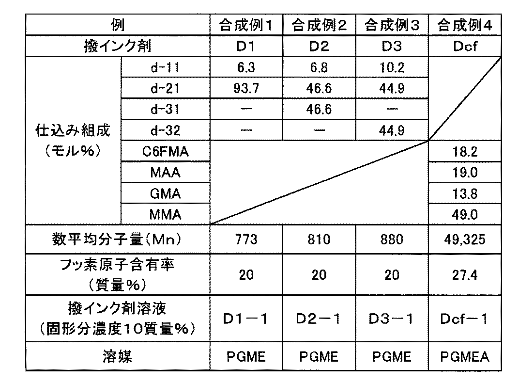
(ネガ型感光性樹脂組成物の調製)
(D1-1)液の0.967g(固形分は0.097g、残りはPGME(溶媒))、EP4020Gの19.34g、MW-100LMの4.84g、CPI-210Sの0.73g、およびPGMEAの74.1gを500cm3の撹拌用容器に入れ、30分間撹拌して、ネガ型感光性樹脂組成物1を調製した。
10cm四方のガラス基板を、エタノールで30秒間超音波洗浄し、次いで、5分間の紫外線/オゾン洗浄を行った。紫外線/オゾン洗浄には、紫外線/オゾン発生装置として、PL7-200(センエジニアリング社製)を使用した。なお、以下の全ての紫外線/オゾン処理についても、紫外線/オゾン発生装置として本装置を使用した。
上記で得られたネガ型感光性樹脂組成物1および硬化膜(隔壁)が形成されたガラス基板(1)について、以下の評価を行った。評価結果をネガ型感光性樹脂組成物の組成とともに表2に示す。
<撥インク性(隔壁)・親インク性(ドット)・現像残渣>
得られたガラス基板(1)の硬化膜、すなわち隔壁表面(露光部分)のPGMEAに対する接触角と、現像により乾燥膜(未露光部分)が除去された部分、すなわちドット部分(ガラス基板表面)の水に対する接触角を測定した。この時、ドット部分の水に対する接触角により現像残渣についての評価も行った。評価は以下の基準で行った。
○(良好):水の接触角が30度未満
×(不良):水の接触角が30度以上
ネガ型感光性樹脂組成物をガラス製スクリュー瓶にて、23℃(室温)で一カ月保存した。一カ月保存後、上記の硬化膜(隔壁)の製造と同様の方法で洗浄した10cm×10cmのガラス基板表面に、スピンナーを用いて、ネガ型感光性樹脂組成物を塗布し、塗膜を形成した。さらに、100℃で2分間、ホットプレート上で乾燥させ、膜厚2μmの乾燥膜を形成した。乾燥膜の外観を目視にて観察し、以下の基準により評価した。
○(良好):乾燥膜上の異物が5個以下である。
×(不良):乾燥膜上の異物が6個以上で、かつガラス基板の中心部から放射状の筋模様が観察された。
(D1-1)液に代えて(D2-1)液を用いた以外は、例1と同様にして、ネガ型感光性樹脂組成物2およびネガ型感光性樹脂組成物2の硬化膜が形成されたガラス基板(2)を作製し、例1と同様にして評価した。
(D1-1)液に代えて(D3-1)液を用いた以外は、例1と同様にして、ネガ型感光性樹脂組成物3およびネガ型感光性樹脂組成物3の硬化膜が形成されたガラス基板(3)を作製し、例1と同様にして評価した。
(D1-1)液に代えて(Dcf-1)液を用いた以外は、例1と同様にして、ネガ型感光性樹脂組成物4およびネガ型感光性樹脂組成物4の硬化膜が形成されたガラス基板(4)を作製し、例1と同様にして評価した。
例2~4の評価結果を、ネガ型感光性樹脂組成物の組成とともに表2に示す。
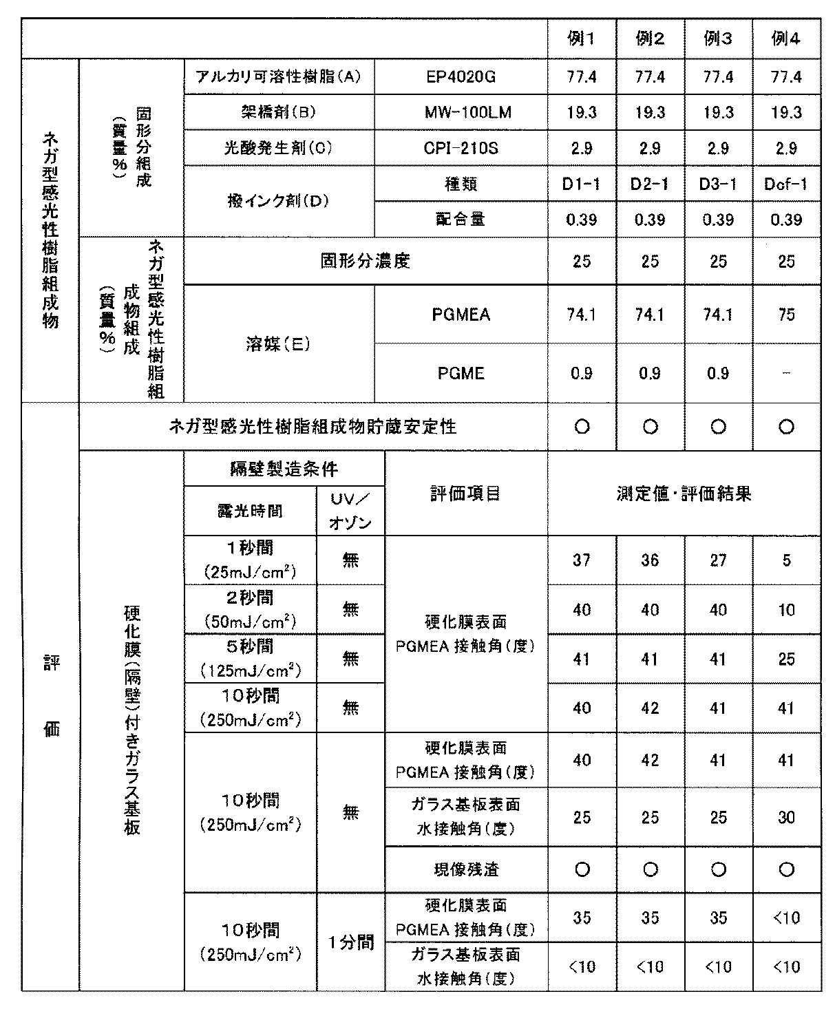
Claims (15)
- アルカリ可溶性樹脂(A)と、架橋剤(B)と、光酸発生剤(C)と、フルオロアルキレン基および/またはフルオロアルキル基と加水分解性基とを有する加水分解性シラン化合物(s1)を単量体および/または部分加水分解(共)縮合物として含む撥インク剤(D)と、を含むネガ型感光性樹脂組成物。
- 前記撥インク剤(D)中のフッ素原子の含有率が1~40質量%である、請求項1に記載のネガ型感光性樹脂組成物。
- 前記撥インク剤(D)は、ケイ素原子に4個の加水分解性基が結合した加水分解性シラン化合物(s2)を単量体および/または部分加水分解(共)縮合物として含む、請求項1または2に記載のネガ型感光性樹脂組成物。
- 前記撥インク剤(D)は、炭化水素基と加水分解性基のみを有する加水分解性シラン化合物(s3)を単量体および/または部分加水分解(共)縮合物として含む、請求項1~3のいずれか1項に記載のネガ型感光性樹脂組成物。
- 前記撥インク剤(D)は、カチオン重合性基と加水分解性基とを有し、フッ素原子を含まない加水分解性シラン化合物(s4)を単量体および/または部分加水分解(共)縮合物として含む、請求項1~4のいずれか1項に記載のネガ型感光性樹脂組成物。
- 前記アルカリ可溶性樹脂(A)の含有量が、ネガ型感光性樹脂組成物における全固形分中、10~90質量%である、請求項1~5のいずれか1項に記載のネガ型感光性樹脂組成物。
- 前記架橋剤(B)、および光酸発生剤の含有量が、アルカリ可溶性樹脂(A)の100質量部に対して、それぞれ2~50質量部、および0.1~20質量部である、請求項1~6のいずれか1項に記載のネガ型感光性樹脂組成物。
- 前記撥インク剤(D)の含有量が、アルカリ可溶性樹脂(A)の100質量部に対して0.01~20質量部である、請求項1~7のいずれか1項に記載のネガ型感光性樹脂組成物。
- さらに、プロピレングリコールモノメチルエーテルアセテート、プロピレングリコールモノメチルエーテル、ジエチレングリコールエチルメチルエーテル、ジエチレングリコールモノエチルエーテルアセテートおよび2-プロパノールからなる群から選
ばれる少なくとも1種の溶媒(E)を含む、請求項1~8のいずれか1項に記載のネガ型感光性樹脂組成物。 - 前記溶媒(E)の含有量が、ネガ型感光性樹脂組成物全量に対して50~99質量%である、請求項1~9のいずれか1項に記載のネガ型感光性樹脂組成物。
- 基板表面をドット形成用の複数の区画に仕切る形に形成された隔壁であって、請求項1~10のいずれか1項に記載のネガ型感光性樹脂組成物の硬化膜からなる隔壁。
- 幅が100μm以下であり、隔壁間の距離(パターンの幅)が300μm以下であり、高さが0.05~50μmである、請求項11に記載の隔壁。
- 基板表面に複数のドットと、隣接するドット間に位置する隔壁とを有する光学素子であって、前記隔壁が請求項11または12に記載の隔壁で形成されていることを特徴とする光学素子。
- 前記ドットがインクジェット法で形成されている、請求項13に記載の光学素子。
- 前記光学素子が、有機EL素子、量子ドットディスプレイ、TFTアレイまたは薄膜太陽電池である、請求項13または14に記載の光学素子。
Priority Applications (3)
| Application Number | Priority Date | Filing Date | Title |
|---|---|---|---|
| KR1020167029324A KR102378162B1 (ko) | 2014-04-25 | 2015-04-22 | 네거티브형 감광성 수지 조성물, 격벽 및 광학 소자 |
| CN201580022166.6A CN106462069B (zh) | 2014-04-25 | 2015-04-22 | 负型感光性树脂组合物、分隔壁及光学元件 |
| JP2016515187A JP6565904B2 (ja) | 2014-04-25 | 2015-04-22 | ネガ型感光性樹脂組成物、隔壁、光学素子および光学素子の製造方法 |
Applications Claiming Priority (2)
| Application Number | Priority Date | Filing Date | Title |
|---|---|---|---|
| JP2014-092092 | 2014-04-25 | ||
| JP2014092092 | 2014-04-25 |
Publications (1)
| Publication Number | Publication Date |
|---|---|
| WO2015163379A1 true WO2015163379A1 (ja) | 2015-10-29 |
Family
ID=54332542
Family Applications (1)
| Application Number | Title | Priority Date | Filing Date |
|---|---|---|---|
| PCT/JP2015/062288 Ceased WO2015163379A1 (ja) | 2014-04-25 | 2015-04-22 | ネガ型感光性樹脂組成物、隔壁および光学素子 |
Country Status (5)
| Country | Link |
|---|---|
| JP (1) | JP6565904B2 (ja) |
| KR (1) | KR102378162B1 (ja) |
| CN (1) | CN106462069B (ja) |
| TW (1) | TWI655501B (ja) |
| WO (1) | WO2015163379A1 (ja) |
Cited By (4)
| Publication number | Priority date | Publication date | Assignee | Title |
|---|---|---|---|---|
| WO2017082307A1 (ja) * | 2015-11-10 | 2017-05-18 | 旭硝子株式会社 | 蛍光分析バイオチップ用感光性組成物、蛍光分析バイオチップの製造方法および蛍光分析バイオチップ |
| WO2019156000A1 (ja) * | 2018-02-08 | 2019-08-15 | 日産化学株式会社 | 感光性樹脂組成物 |
| WO2021053793A1 (ja) * | 2019-09-19 | 2021-03-25 | シャープ株式会社 | 発光デバイスおよび発光デバイスの製造方法 |
| JP2022167815A (ja) * | 2021-04-23 | 2022-11-04 | 住友ベークライト株式会社 | 光導波路形成用感光性樹脂組成物、光導波路、および光導波路の製造方法 |
Families Citing this family (2)
| Publication number | Priority date | Publication date | Assignee | Title |
|---|---|---|---|---|
| WO2018116914A1 (ja) * | 2016-12-22 | 2018-06-28 | 旭硝子株式会社 | ネガ型感光性樹脂組成物 |
| CN110412829A (zh) * | 2018-04-26 | 2019-11-05 | 东友精细化工有限公司 | 负型感光性树脂组合物、光固化图案及图像显示装置 |
Citations (15)
| Publication number | Priority date | Publication date | Assignee | Title |
|---|---|---|---|---|
| JP2004277494A (ja) * | 2003-03-13 | 2004-10-07 | Asahi Glass Co Ltd | 含フッ素樹脂および感光性樹脂組成物 |
| JP2005148391A (ja) * | 2003-11-14 | 2005-06-09 | Tokyo Ohka Kogyo Co Ltd | 隔壁形成用レジスト組成物、el表示素子の隔壁、およびel表示素子 |
| WO2010013816A1 (ja) * | 2008-08-01 | 2010-02-04 | 旭硝子株式会社 | ネガ型感光性組成物、それを用いた光学素子用隔壁および該隔壁を有する光学素子 |
| WO2012074076A1 (ja) * | 2010-12-01 | 2012-06-07 | 日産化学工業株式会社 | 含フッ素高分岐ポリマー及びそれを含む感光性組成物 |
| WO2012077770A1 (ja) * | 2010-12-10 | 2012-06-14 | 旭硝子株式会社 | ネガ型感光性樹脂組成物、光学素子用隔壁およびその製造方法、該隔壁を有する光学素子の製造方法、ならびに、撥インク剤溶液 |
| WO2012132755A1 (ja) * | 2011-03-31 | 2012-10-04 | 旭硝子株式会社 | ネガ型感光性樹脂組成物および塗膜 |
| WO2012147626A1 (ja) * | 2011-04-28 | 2012-11-01 | 旭硝子株式会社 | ネガ型感光性樹脂組成物、硬化膜、隔壁およびブラックマトリックスとその製造方法、カラーフィルタならびに有機el素子 |
| WO2012176816A1 (ja) * | 2011-06-21 | 2012-12-27 | 旭硝子株式会社 | ネガ型感光性樹脂組成物、隔壁、ブラックマトリックス、カラーフィルタおよび液晶表示素子 |
| JP2013043864A (ja) * | 2011-08-25 | 2013-03-04 | San Apro Kk | スルホニウム塩、光酸発生剤、硬化性組成物およびレジスト組成物 |
| WO2013058386A1 (ja) * | 2011-10-21 | 2013-04-25 | 旭硝子株式会社 | 撥インク剤の製造方法、ネガ型感光性樹脂組成物、隔壁および光学素子 |
| WO2013069789A1 (ja) * | 2011-11-11 | 2013-05-16 | 旭硝子株式会社 | ネガ型感光性樹脂組成物、隔壁、ブラックマトリックス及び光学素子 |
| WO2013133392A1 (ja) * | 2012-03-09 | 2013-09-12 | 旭硝子株式会社 | ポジ型感光性樹脂組成物、隔壁及び光学素子 |
| WO2013161829A1 (ja) * | 2012-04-27 | 2013-10-31 | 旭硝子株式会社 | 部分加水分解縮合物、撥インク剤、ネガ型感光性樹脂組成物、硬化膜、隔壁および光学素子 |
| WO2014046210A1 (ja) * | 2012-09-24 | 2014-03-27 | 旭硝子株式会社 | 部分加水分解縮合物およびこれを用いた撥インク剤 |
| WO2014046209A1 (ja) * | 2012-09-24 | 2014-03-27 | 旭硝子株式会社 | 撥インク性組成物、ネガ型感光性樹脂組成物、硬化膜、隔壁、及び光学素子 |
Family Cites Families (10)
| Publication number | Priority date | Publication date | Assignee | Title |
|---|---|---|---|---|
| JP2002131908A (ja) * | 2000-10-20 | 2002-05-09 | Fuji Photo Film Co Ltd | 電子線又はx線用ネガ型レジスト組成物 |
| JP4217441B2 (ja) * | 2001-08-21 | 2009-02-04 | 富士フイルム株式会社 | 感刺激性組成物及び化合物 |
| JP2003082042A (ja) * | 2001-09-07 | 2003-03-19 | Jsr Corp | 隔壁形成用感放射線性樹脂組成物、隔壁、および表示素子。 |
| JP2003330174A (ja) * | 2002-05-14 | 2003-11-19 | Sumitomo Chem Co Ltd | 着色感光性樹脂組成物 |
| JP4337631B2 (ja) * | 2003-05-20 | 2009-09-30 | 日油株式会社 | 含フッ素カルボン酸誘導体、硬化性樹脂組成物およびその用途 |
| JP2005345897A (ja) * | 2004-06-04 | 2005-12-15 | Asahi Glass Co Ltd | 撥水性組成物、撥水性薄膜および撥水性親水性パターンを有する薄膜 |
| JP5126222B2 (ja) * | 2007-04-25 | 2013-01-23 | 旭硝子株式会社 | 感光性組成物、隔壁、ブラックマトリックス、カラーフィルタの製造方法 |
| JP2009244779A (ja) * | 2008-03-31 | 2009-10-22 | Fujifilm Corp | ネガ型レジスト組成物及びパターン形成方法 |
| JP5422402B2 (ja) * | 2010-01-08 | 2014-02-19 | 富士フイルム株式会社 | パターン形成方法、化学増幅型レジスト組成物及びレジスト膜 |
| CN103189797A (zh) * | 2010-10-29 | 2013-07-03 | 住友化学株式会社 | 感光性树脂组合物、图案构造物、显示装置及隔壁 |
-
2015
- 2015-04-22 CN CN201580022166.6A patent/CN106462069B/zh not_active Expired - Fee Related
- 2015-04-22 KR KR1020167029324A patent/KR102378162B1/ko not_active Expired - Fee Related
- 2015-04-22 JP JP2016515187A patent/JP6565904B2/ja active Active
- 2015-04-22 WO PCT/JP2015/062288 patent/WO2015163379A1/ja not_active Ceased
- 2015-04-23 TW TW104113066A patent/TWI655501B/zh not_active IP Right Cessation
Patent Citations (15)
| Publication number | Priority date | Publication date | Assignee | Title |
|---|---|---|---|---|
| JP2004277494A (ja) * | 2003-03-13 | 2004-10-07 | Asahi Glass Co Ltd | 含フッ素樹脂および感光性樹脂組成物 |
| JP2005148391A (ja) * | 2003-11-14 | 2005-06-09 | Tokyo Ohka Kogyo Co Ltd | 隔壁形成用レジスト組成物、el表示素子の隔壁、およびel表示素子 |
| WO2010013816A1 (ja) * | 2008-08-01 | 2010-02-04 | 旭硝子株式会社 | ネガ型感光性組成物、それを用いた光学素子用隔壁および該隔壁を有する光学素子 |
| WO2012074076A1 (ja) * | 2010-12-01 | 2012-06-07 | 日産化学工業株式会社 | 含フッ素高分岐ポリマー及びそれを含む感光性組成物 |
| WO2012077770A1 (ja) * | 2010-12-10 | 2012-06-14 | 旭硝子株式会社 | ネガ型感光性樹脂組成物、光学素子用隔壁およびその製造方法、該隔壁を有する光学素子の製造方法、ならびに、撥インク剤溶液 |
| WO2012132755A1 (ja) * | 2011-03-31 | 2012-10-04 | 旭硝子株式会社 | ネガ型感光性樹脂組成物および塗膜 |
| WO2012147626A1 (ja) * | 2011-04-28 | 2012-11-01 | 旭硝子株式会社 | ネガ型感光性樹脂組成物、硬化膜、隔壁およびブラックマトリックスとその製造方法、カラーフィルタならびに有機el素子 |
| WO2012176816A1 (ja) * | 2011-06-21 | 2012-12-27 | 旭硝子株式会社 | ネガ型感光性樹脂組成物、隔壁、ブラックマトリックス、カラーフィルタおよび液晶表示素子 |
| JP2013043864A (ja) * | 2011-08-25 | 2013-03-04 | San Apro Kk | スルホニウム塩、光酸発生剤、硬化性組成物およびレジスト組成物 |
| WO2013058386A1 (ja) * | 2011-10-21 | 2013-04-25 | 旭硝子株式会社 | 撥インク剤の製造方法、ネガ型感光性樹脂組成物、隔壁および光学素子 |
| WO2013069789A1 (ja) * | 2011-11-11 | 2013-05-16 | 旭硝子株式会社 | ネガ型感光性樹脂組成物、隔壁、ブラックマトリックス及び光学素子 |
| WO2013133392A1 (ja) * | 2012-03-09 | 2013-09-12 | 旭硝子株式会社 | ポジ型感光性樹脂組成物、隔壁及び光学素子 |
| WO2013161829A1 (ja) * | 2012-04-27 | 2013-10-31 | 旭硝子株式会社 | 部分加水分解縮合物、撥インク剤、ネガ型感光性樹脂組成物、硬化膜、隔壁および光学素子 |
| WO2014046210A1 (ja) * | 2012-09-24 | 2014-03-27 | 旭硝子株式会社 | 部分加水分解縮合物およびこれを用いた撥インク剤 |
| WO2014046209A1 (ja) * | 2012-09-24 | 2014-03-27 | 旭硝子株式会社 | 撥インク性組成物、ネガ型感光性樹脂組成物、硬化膜、隔壁、及び光学素子 |
Cited By (5)
| Publication number | Priority date | Publication date | Assignee | Title |
|---|---|---|---|---|
| WO2017082307A1 (ja) * | 2015-11-10 | 2017-05-18 | 旭硝子株式会社 | 蛍光分析バイオチップ用感光性組成物、蛍光分析バイオチップの製造方法および蛍光分析バイオチップ |
| WO2019156000A1 (ja) * | 2018-02-08 | 2019-08-15 | 日産化学株式会社 | 感光性樹脂組成物 |
| WO2021053793A1 (ja) * | 2019-09-19 | 2021-03-25 | シャープ株式会社 | 発光デバイスおよび発光デバイスの製造方法 |
| US12356788B2 (en) | 2019-09-19 | 2025-07-08 | Sharp Kabushiki Kaisha | Light emitting device and method for manufacturing light emitting device |
| JP2022167815A (ja) * | 2021-04-23 | 2022-11-04 | 住友ベークライト株式会社 | 光導波路形成用感光性樹脂組成物、光導波路、および光導波路の製造方法 |
Also Published As
| Publication number | Publication date |
|---|---|
| KR102378162B1 (ko) | 2022-03-23 |
| TW201546546A (zh) | 2015-12-16 |
| CN106462069A (zh) | 2017-02-22 |
| CN106462069B (zh) | 2019-10-18 |
| JP6565904B2 (ja) | 2019-08-28 |
| KR20160146719A (ko) | 2016-12-21 |
| TWI655501B (zh) | 2019-04-01 |
| JPWO2015163379A1 (ja) | 2017-04-20 |
Similar Documents
| Publication | Publication Date | Title |
|---|---|---|
| KR101817378B1 (ko) | 감광성 수지 조성물, 격벽, 컬러 필터 및 유기 el 소자 | |
| JP6536578B2 (ja) | ネガ型感光性樹脂組成物、樹脂硬化膜、隔壁、光学素子および光学素子の製造方法 | |
| JP6350287B2 (ja) | ネガ型感光性樹脂組成物、樹脂硬化膜、隔壁及び光学素子 | |
| KR101810402B1 (ko) | 감광성 수지 조성물 및 디스플레이 장치 | |
| JP6565904B2 (ja) | ネガ型感光性樹脂組成物、隔壁、光学素子および光学素子の製造方法 | |
| JP5803938B2 (ja) | ネガ型感光性樹脂組成物、光学素子用隔壁およびその製造方法、ならびに、該隔壁を有する光学素子の製造方法 | |
| TWI734756B (zh) | 感光性矽氧烷組成物及硬化膜的形成方法 | |
| CN103765314B (zh) | 负型感光性树脂组合物、分隔壁以及光学元件 | |
| CN102112923A (zh) | 负型感光性组合物、使用该组合物的光学元件用间隔壁及具有该间隔壁的光学元件 | |
| TWI629566B (zh) | 負型感光性樹脂組成物、樹脂硬化膜、隔壁及光學元件 | |
| WO2015093415A1 (ja) | ネガ型感光性樹脂組成物、樹脂硬化膜、隔壁および光学素子 | |
| TW201321898A (zh) | 撥墨劑之製造方法、負型感光性樹脂組成物、隔壁及光學元件 | |
| US20210208503A1 (en) | Negative type photosensitive composition curable at low temperature | |
| JP5346787B2 (ja) | 硬化性樹脂組成物及びその硬化物 | |
| JP7010240B2 (ja) | ネガ型感光性樹脂組成物 | |
| TW201421163A (zh) | 部分水解縮合物及使用其之撥墨劑 | |
| JP2017040869A (ja) | ネガ型感光性樹脂組成物、樹脂硬化膜、隔壁ならびに光学素子およびその製造方法 | |
| WO2017033835A1 (ja) | ネガ型感光性樹脂組成物、樹脂硬化膜、隔壁ならびに光学素子およびその製造方法 | |
| WO2017033834A1 (ja) | ネガ型感光性樹脂組成物、樹脂硬化膜、隔壁ならびに光学素子およびその製造方法 | |
| WO2024038814A1 (ja) | ポジ型感光性樹脂組成物、隔壁および光学素子 | |
| JP2005250203A (ja) | ポジ型スペーサー用樹脂組成物および接着性スペーサーの製造方法 |
Legal Events
| Date | Code | Title | Description |
|---|---|---|---|
| 121 | Ep: the epo has been informed by wipo that ep was designated in this application |
Ref document number: 15782229 Country of ref document: EP Kind code of ref document: A1 |
|
| ENP | Entry into the national phase |
Ref document number: 2016515187 Country of ref document: JP Kind code of ref document: A |
|
| ENP | Entry into the national phase |
Ref document number: 20167029324 Country of ref document: KR Kind code of ref document: A |
|
| NENP | Non-entry into the national phase |
Ref country code: DE |
|
| 122 | Ep: pct application non-entry in european phase |
Ref document number: 15782229 Country of ref document: EP Kind code of ref document: A1 |