WO2015072260A1 - Détecteur de rayonnement, et méthode de production de détecteur de rayonnement - Google Patents
Détecteur de rayonnement, et méthode de production de détecteur de rayonnement Download PDFInfo
- Publication number
- WO2015072260A1 WO2015072260A1 PCT/JP2014/077252 JP2014077252W WO2015072260A1 WO 2015072260 A1 WO2015072260 A1 WO 2015072260A1 JP 2014077252 W JP2014077252 W JP 2014077252W WO 2015072260 A1 WO2015072260 A1 WO 2015072260A1
- Authority
- WO
- WIPO (PCT)
- Prior art keywords
- resin frame
- scintillator layer
- photoelectric conversion
- protective film
- outer edge
- Prior art date
Links
- 230000005855 radiation Effects 0.000 title claims abstract description 75
- 238000004519 manufacturing process Methods 0.000 title claims description 26
- 239000011347 resin Substances 0.000 claims abstract description 164
- 229920005989 resin Polymers 0.000 claims abstract description 164
- 230000001681 protective effect Effects 0.000 claims abstract description 87
- 238000006243 chemical reaction Methods 0.000 claims abstract description 69
- 239000011248 coating agent Substances 0.000 claims description 19
- 238000000576 coating method Methods 0.000 claims description 19
- 238000000034 method Methods 0.000 claims description 13
- 230000002093 peripheral effect Effects 0.000 claims description 10
- 229910052751 metal Inorganic materials 0.000 claims description 7
- 239000002184 metal Substances 0.000 claims description 7
- 238000010030 laminating Methods 0.000 claims description 6
- 230000007423 decrease Effects 0.000 claims description 4
- 230000001678 irradiating effect Effects 0.000 claims description 4
- 239000010408 film Substances 0.000 description 131
- 230000002411 adverse Effects 0.000 description 14
- 230000000694 effects Effects 0.000 description 12
- 239000000758 substrate Substances 0.000 description 10
- CURLTUGMZLYLDI-UHFFFAOYSA-N Carbon dioxide Chemical compound O=C=O CURLTUGMZLYLDI-UHFFFAOYSA-N 0.000 description 8
- 230000015572 biosynthetic process Effects 0.000 description 7
- 238000005520 cutting process Methods 0.000 description 7
- 238000001514 detection method Methods 0.000 description 7
- 238000002161 passivation Methods 0.000 description 5
- -1 polyparaxylylene Polymers 0.000 description 5
- XQPRBTXUXXVTKB-UHFFFAOYSA-M caesium iodide Chemical compound [I-].[Cs+] XQPRBTXUXXVTKB-UHFFFAOYSA-M 0.000 description 4
- 229910002092 carbon dioxide Inorganic materials 0.000 description 4
- 239000001569 carbon dioxide Substances 0.000 description 4
- 229920000052 poly(p-xylylene) Polymers 0.000 description 4
- 230000007797 corrosion Effects 0.000 description 3
- 238000005260 corrosion Methods 0.000 description 3
- 239000000463 material Substances 0.000 description 3
- XUIMIQQOPSSXEZ-UHFFFAOYSA-N Silicon Chemical compound [Si] XUIMIQQOPSSXEZ-UHFFFAOYSA-N 0.000 description 2
- 239000003522 acrylic cement Substances 0.000 description 2
- 238000005229 chemical vapour deposition Methods 0.000 description 2
- 239000011651 chromium Substances 0.000 description 2
- 239000013078 crystal Substances 0.000 description 2
- 230000006866 deterioration Effects 0.000 description 2
- 230000035945 sensitivity Effects 0.000 description 2
- 229910052710 silicon Inorganic materials 0.000 description 2
- 239000010703 silicon Substances 0.000 description 2
- 239000010936 titanium Substances 0.000 description 2
- 238000007740 vapor deposition Methods 0.000 description 2
- XLYOFNOQVPJJNP-UHFFFAOYSA-N water Chemical compound O XLYOFNOQVPJJNP-UHFFFAOYSA-N 0.000 description 2
- 239000004925 Acrylic resin Substances 0.000 description 1
- 229920000178 Acrylic resin Polymers 0.000 description 1
- VYZAMTAEIAYCRO-UHFFFAOYSA-N Chromium Chemical compound [Cr] VYZAMTAEIAYCRO-UHFFFAOYSA-N 0.000 description 1
- 229910052581 Si3N4 Inorganic materials 0.000 description 1
- VYPSYNLAJGMNEJ-UHFFFAOYSA-N Silicium dioxide Chemical compound O=[Si]=O VYPSYNLAJGMNEJ-UHFFFAOYSA-N 0.000 description 1
- BQCADISMDOOEFD-UHFFFAOYSA-N Silver Chemical compound [Ag] BQCADISMDOOEFD-UHFFFAOYSA-N 0.000 description 1
- RTAQQCXQSZGOHL-UHFFFAOYSA-N Titanium Chemical compound [Ti] RTAQQCXQSZGOHL-UHFFFAOYSA-N 0.000 description 1
- 238000010521 absorption reaction Methods 0.000 description 1
- 229910052782 aluminium Inorganic materials 0.000 description 1
- XAGFODPZIPBFFR-UHFFFAOYSA-N aluminium Chemical compound [Al] XAGFODPZIPBFFR-UHFFFAOYSA-N 0.000 description 1
- 229910021417 amorphous silicon Inorganic materials 0.000 description 1
- 230000000903 blocking effect Effects 0.000 description 1
- 229910052804 chromium Inorganic materials 0.000 description 1
- 239000011521 glass Substances 0.000 description 1
- PCHJSUWPFVWCPO-UHFFFAOYSA-N gold Chemical compound [Au] PCHJSUWPFVWCPO-UHFFFAOYSA-N 0.000 description 1
- 239000010931 gold Substances 0.000 description 1
- 229910052737 gold Inorganic materials 0.000 description 1
- 238000003672 processing method Methods 0.000 description 1
- 239000004065 semiconductor Substances 0.000 description 1
- HQVNEWCFYHHQES-UHFFFAOYSA-N silicon nitride Chemical compound N12[Si]34N5[Si]62N3[Si]51N64 HQVNEWCFYHHQES-UHFFFAOYSA-N 0.000 description 1
- 229910052814 silicon oxide Inorganic materials 0.000 description 1
- 229910052709 silver Inorganic materials 0.000 description 1
- 239000004332 silver Substances 0.000 description 1
- 229910052716 thallium Inorganic materials 0.000 description 1
- BKVIYDNLLOSFOA-UHFFFAOYSA-N thallium Chemical compound [Tl] BKVIYDNLLOSFOA-UHFFFAOYSA-N 0.000 description 1
- 230000003685 thermal hair damage Effects 0.000 description 1
- 239000010409 thin film Substances 0.000 description 1
- 229910052719 titanium Inorganic materials 0.000 description 1
Images


Classifications
-
- G—PHYSICS
- G01—MEASURING; TESTING
- G01T—MEASUREMENT OF NUCLEAR OR X-RADIATION
- G01T1/00—Measuring X-radiation, gamma radiation, corpuscular radiation, or cosmic radiation
- G01T1/16—Measuring radiation intensity
- G01T1/20—Measuring radiation intensity with scintillation detectors
- G01T1/2002—Optical details, e.g. reflecting or diffusing layers
-
- G—PHYSICS
- G01—MEASURING; TESTING
- G01T—MEASUREMENT OF NUCLEAR OR X-RADIATION
- G01T1/00—Measuring X-radiation, gamma radiation, corpuscular radiation, or cosmic radiation
- G01T1/16—Measuring radiation intensity
- G01T1/20—Measuring radiation intensity with scintillation detectors
- G01T1/2018—Scintillation-photodiode combinations
- G01T1/20188—Auxiliary details, e.g. casings or cooling
- G01T1/20189—Damping or insulation against damage, e.g. caused by heat or pressure
-
- G—PHYSICS
- G01—MEASURING; TESTING
- G01T—MEASUREMENT OF NUCLEAR OR X-RADIATION
- G01T1/00—Measuring X-radiation, gamma radiation, corpuscular radiation, or cosmic radiation
- G01T1/16—Measuring radiation intensity
- G01T1/20—Measuring radiation intensity with scintillation detectors
- G01T1/2018—Scintillation-photodiode combinations
- G01T1/20187—Position of the scintillator with respect to the photodiode, e.g. photodiode surrounding the crystal, the crystal surrounding the photodiode, shape or size of the scintillator
-
- G—PHYSICS
- G01—MEASURING; TESTING
- G01T—MEASUREMENT OF NUCLEAR OR X-RADIATION
- G01T1/00—Measuring X-radiation, gamma radiation, corpuscular radiation, or cosmic radiation
- G01T1/16—Measuring radiation intensity
- G01T1/20—Measuring radiation intensity with scintillation detectors
- G01T1/2018—Scintillation-photodiode combinations
- G01T1/20188—Auxiliary details, e.g. casings or cooling
-
- H—ELECTRICITY
- H01—ELECTRIC ELEMENTS
- H01L—SEMICONDUCTOR DEVICES NOT COVERED BY CLASS H10
- H01L27/00—Devices consisting of a plurality of semiconductor or other solid-state components formed in or on a common substrate
- H01L27/14—Devices consisting of a plurality of semiconductor or other solid-state components formed in or on a common substrate including semiconductor components sensitive to infrared radiation, light, electromagnetic radiation of shorter wavelength or corpuscular radiation and specially adapted either for the conversion of the energy of such radiation into electrical energy or for the control of electrical energy by such radiation
- H01L27/144—Devices controlled by radiation
- H01L27/146—Imager structures
- H01L27/14601—Structural or functional details thereof
- H01L27/14618—Containers
-
- H—ELECTRICITY
- H01—ELECTRIC ELEMENTS
- H01L—SEMICONDUCTOR DEVICES NOT COVERED BY CLASS H10
- H01L27/00—Devices consisting of a plurality of semiconductor or other solid-state components formed in or on a common substrate
- H01L27/14—Devices consisting of a plurality of semiconductor or other solid-state components formed in or on a common substrate including semiconductor components sensitive to infrared radiation, light, electromagnetic radiation of shorter wavelength or corpuscular radiation and specially adapted either for the conversion of the energy of such radiation into electrical energy or for the control of electrical energy by such radiation
- H01L27/144—Devices controlled by radiation
- H01L27/146—Imager structures
- H01L27/14601—Structural or functional details thereof
- H01L27/1462—Coatings
-
- H—ELECTRICITY
- H01—ELECTRIC ELEMENTS
- H01L—SEMICONDUCTOR DEVICES NOT COVERED BY CLASS H10
- H01L27/00—Devices consisting of a plurality of semiconductor or other solid-state components formed in or on a common substrate
- H01L27/14—Devices consisting of a plurality of semiconductor or other solid-state components formed in or on a common substrate including semiconductor components sensitive to infrared radiation, light, electromagnetic radiation of shorter wavelength or corpuscular radiation and specially adapted either for the conversion of the energy of such radiation into electrical energy or for the control of electrical energy by such radiation
- H01L27/144—Devices controlled by radiation
- H01L27/146—Imager structures
- H01L27/14601—Structural or functional details thereof
- H01L27/14625—Optical elements or arrangements associated with the device
- H01L27/14629—Reflectors
-
- H—ELECTRICITY
- H01—ELECTRIC ELEMENTS
- H01L—SEMICONDUCTOR DEVICES NOT COVERED BY CLASS H10
- H01L27/00—Devices consisting of a plurality of semiconductor or other solid-state components formed in or on a common substrate
- H01L27/14—Devices consisting of a plurality of semiconductor or other solid-state components formed in or on a common substrate including semiconductor components sensitive to infrared radiation, light, electromagnetic radiation of shorter wavelength or corpuscular radiation and specially adapted either for the conversion of the energy of such radiation into electrical energy or for the control of electrical energy by such radiation
- H01L27/144—Devices controlled by radiation
- H01L27/146—Imager structures
- H01L27/14601—Structural or functional details thereof
- H01L27/14636—Interconnect structures
-
- H—ELECTRICITY
- H01—ELECTRIC ELEMENTS
- H01L—SEMICONDUCTOR DEVICES NOT COVERED BY CLASS H10
- H01L27/00—Devices consisting of a plurality of semiconductor or other solid-state components formed in or on a common substrate
- H01L27/14—Devices consisting of a plurality of semiconductor or other solid-state components formed in or on a common substrate including semiconductor components sensitive to infrared radiation, light, electromagnetic radiation of shorter wavelength or corpuscular radiation and specially adapted either for the conversion of the energy of such radiation into electrical energy or for the control of electrical energy by such radiation
- H01L27/144—Devices controlled by radiation
- H01L27/146—Imager structures
- H01L27/14643—Photodiode arrays; MOS imagers
- H01L27/14658—X-ray, gamma-ray or corpuscular radiation imagers
- H01L27/14663—Indirect radiation imagers, e.g. using luminescent members
-
- H—ELECTRICITY
- H01—ELECTRIC ELEMENTS
- H01L—SEMICONDUCTOR DEVICES NOT COVERED BY CLASS H10
- H01L27/00—Devices consisting of a plurality of semiconductor or other solid-state components formed in or on a common substrate
- H01L27/14—Devices consisting of a plurality of semiconductor or other solid-state components formed in or on a common substrate including semiconductor components sensitive to infrared radiation, light, electromagnetic radiation of shorter wavelength or corpuscular radiation and specially adapted either for the conversion of the energy of such radiation into electrical energy or for the control of electrical energy by such radiation
- H01L27/144—Devices controlled by radiation
- H01L27/146—Imager structures
- H01L27/14683—Processes or apparatus peculiar to the manufacture or treatment of these devices or parts thereof
- H01L27/14685—Process for coatings or optical elements
Definitions
- the present invention relates to a radiation detector and a method for manufacturing the radiation detector.
- a radiation detector (radiation detection element) in which a scintillator layer having a columnar crystal structure is formed on a sensor panel (light receiving portion) is known.
- a plurality of bonding pads that are electrically connected to the light receiving element are disposed outside the light receiving portion.
- a resin frame is formed so as to pass between the scintillator layer and the bonding pad and surround the scintillator layer when viewed from the stacking direction of the scintillator layer.
- the scintillator layer is covered with a moisture-resistant protective film, and the outer edge of the moisture-resistant protective film reaches the resin frame.
- the resin frame is made as small as possible, and the distance between the resin frame and the outer edge of the scintillator layer is made as short as possible, so that the area (effective area) of the scintillator layer in the inner region of the resin frame Is preferably as large as possible.
- the moisture-resistant protective film formed on the resin frame is cut by a cutter along the resin frame.
- the work of cutting the moisture-resistant protective film with a cutter in a state where the resin frame is downsized and the distance between the resin frame and the outer edge of the scintillator layer is shortened requires considerable skill. There is room for improvement from the point of view.
- an object of the present invention is to provide a radiation detector that can reduce the size of the apparatus and increase the effective area of the scintillator layer and improve the productivity, and a method for manufacturing the same.
- a radiation detector includes a light receiving unit including a plurality of photoelectric conversion elements arranged one-dimensionally or two-dimensionally, and is electrically connected to the photoelectric conversion elements and disposed outside the light receiving unit.
- a photoelectric conversion element array having a plurality of bonding pads, a scintillator layer that is stacked on the photoelectric conversion element array so as to cover the light receiving portion, and converts radiation into light, and a scintillator layer when viewed from the stacking direction of the scintillator layers
- a resin frame formed on the photoelectric conversion element array so as to pass through the space between the scintillator layer and the bonding pad and surround the scintillator layer, and to cover the scintillator layer and to be positioned on the resin frame
- a first distance between the inner edge of the resin frame and the outer edge of the scintillator layer is defined by: Corresponding region corresponding to the outer edge of the protective film is shorter than the second distance, the outer edge of the protective film,
- the protective film on the resin frame is processed by laser light. Since processing with laser light does not require skilled techniques compared to cutting with a cutter, productivity can be improved. Further, according to the laser beam, the protective film can be cut with high accuracy, so that the resin frame can be reduced in size. In addition, since the resin frame is formed apart from the scintillator layer and the bonding pad, it is possible to suppress an adverse effect on the scintillator layer and the bonding pad due to the laser light during manufacturing. On the other hand, the effective area of the scintillator layer is increased by arranging the resin frame close to the scintillator layer. Therefore, according to the radiation detector according to one aspect of the present invention, it is possible to reduce the size of the apparatus and increase the effective area of the scintillator layer, and to improve the productivity.
- the outer edge and the corresponding region of the protective film may have a fine wave shape when viewed from the stacking direction.
- the contact area between the outer edge of the protective film and the corresponding region and the coating resin increases, so that the outer edge of the protective film and the corresponding region and the coating resin are bonded. It can be made stronger.
- the height of the corresponding region may be 1/3 or less of the height of the resin frame.
- the ratio of the second distance to the first distance may be 5 or more. By setting such a ratio, it is possible to more effectively suppress the adverse effect of the laser beam on the bonding pad during manufacturing, secure the effective area of the scintillator layer, and reduce the size of the device.
- the resin frame is formed so that the center part is higher than both edge parts, and the height of the resin frame may be lower than the height of the scintillator layer.
- the width between the inner edge of the resin frame and the outer edge of the resin frame may be 900 ⁇ m or less, and the height of the resin frame may be 450 ⁇ m or less.
- the outer edge and the corresponding region of the protective film processed by the laser beam may be formed in a substantially rectangular shape having arc-shaped corner portions protruding outward when viewed from the stacking direction.
- the protective film is peeled off from the resin frame at the corners by forming the corners (the corners of the four corners) of the protective film into an arc shape protruding outward (so-called R shape). Can be suppressed.
- the radiation detector may further include a coating resin layer disposed along the resin frame so as to cover the outer edge of the protective film.
- a coating resin layer disposed along the resin frame so as to cover the outer edge of the protective film.
- the peripheral edge of the scintillator layer may have a tapered shape whose height gradually decreases toward the outside of the scintillator layer. In this way, by setting the height of the peripheral edge of the scintillator layer to be lower toward the outer side, it is possible to limit a region where the adverse effect of the laser beam reaches the scintillator layer during manufacturing.
- the protective film may include a metal film that reflects light. Thereby, it is possible to prevent the light generated in the scintillator layer from leaking outside, and to improve the detection sensitivity of the radiation detector.
- a method of manufacturing a radiation detector includes a light receiving unit including a plurality of photoelectric conversion elements arranged one-dimensionally or two-dimensionally, and electrically connected to the photoelectric conversion elements and outside the light receiving unit.
- the first step between the inner edge of the resin frame and the outer edge of the scintillator layer is performed.
- the resin frame is formed so that the distance is shorter than the second distance between the outer edge of the resin frame and the outer edge of the photoelectric conversion element array.
- the protective film on the resin frame is cut by the laser beam, skill is not required compared with cutting by a cutter, and productivity is increased. Can be improved. Further, since the protective film can be cut with high precision by laser light, the resin frame can be reduced in size. In addition, by forming the resin frame away from the scintillator layer and the bonding pad, it is possible to suppress an adverse effect on the scintillator layer and the bonding pad due to the laser light when the protective film is cut. On the other hand, the effective area of the scintillator layer can be increased by forming the resin frame close to the scintillator layer.
- the present invention it is possible to provide a radiation detector that can reduce the size of the apparatus and increase the effective area of the scintillator layer and improve the productivity, and a method for manufacturing the same.
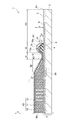
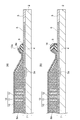
- FIG. 2 is a cross-sectional view taken along line II-II in FIG.
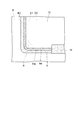
- FIG. 2 is an enlarged plan view near the corner of the radiation detector in FIG. 1.
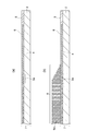
- It is sectional drawing which shows the state before (a) scintillator layer formation in the manufacturing process of the radiation detector of FIG. 1, and the state after (b) scintillator layer formation.
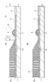
- It is sectional drawing which shows the state after (a) resin frame formation in the manufacturing process of the radiation detector of FIG. 1, and (b) the state after 1st organic film formation.
- the radiation detector 1 includes a photoelectric conversion element array 7, a scintillator layer 8, a resin frame 9, a protective film 13, and a coating resin layer 14.
- the photoelectric conversion element array 7 includes a substrate 2, a light receiving unit 3, a signal line 4, a bonding pad 5, and a passivation film 6.
- the protective film 13 includes a first organic film 10, an inorganic film (metal film) 11, and a second organic film 12.
- the light receiving unit 3 includes a plurality of photoelectric conversion elements 3a arranged two-dimensionally in a rectangular region at the center of an insulating substrate 2 (for example, a glass substrate).
- the photoelectric conversion element 3a is configured by an amorphous silicon photodiode (PD), a thin film transistor (TFT), or the like.
- PD amorphous silicon photodiode
- TFT thin film transistor
- Each of the photoelectric conversion elements 3a in each row or each column in the light receiving unit 3 is electrically connected to a bonding pad 5 for taking out a signal to an external circuit (not shown) by a signal readout signal line 4.
- a plurality of bonding pads 5 are arranged at predetermined intervals along two adjacent sides (the upper side and the right side in FIG. 1) of the outer edges of the substrate 2, and a plurality of corresponding photoelectric conversion elements 3 a via the signal lines 4. Is electrically connected.
- An insulating passivation film 6 is formed on the photoelectric conversion element 3 a and the signal line 4.
- silicon nitride or silicon oxide can be used for the passivation film 6.
- the bonding pad 5 is exposed for connection with an external circuit.
- a columnar scintillator 8 a that converts X-rays (radiation) into light is stacked on the photoelectric conversion element array 7 so as to cover the light receiving unit 3.
- the scintillator layer 8 is formed by laminating a plurality of scintillators 8a in a substantially rectangular region including the light receiving portion 3 in the photoelectric conversion element array 7 (region surrounded by a broken line in FIG. 1).
- Various materials can be used for the scintillator 8a. For example, thallium (Tl) -doped cesium iodide (CsI) having high luminous efficiency can be used.
- the peripheral edge 8b of the scintillator layer 8 has a tapered shape in which the height gradually decreases toward the outside of the scintillator layer 8. That is, the height of the scintillator 8a formed on the outer side of the scintillator layer 8 is lower at the peripheral edge 8b.
- the peripheral edge 8b is an area where the light receiving part 3 is not formed below (an area outside the effective screen), or an area having a small influence on X-ray image generation. Therefore, by providing such a tapered peripheral portion 8b, it is possible to limit the region on the scintillator layer 8 that is adversely affected by laser light during manufacturing.
- the inclination angle of the peripheral edge 8b that is, the angle ⁇ formed by the straight line connecting the scintillator 8a height position formed on the peripheral edge 8b from the inside to the outside of the scintillator layer 8 with respect to the upper surface of the substrate 2 is , Included in the range of 20 to 80 degrees.
- the resin frame 9 is formed on the photoelectric conversion element array 7 so as to pass between the scintillator layer 8 and the bonding pad 5 and surround the scintillator layer 8 when viewed from the stacking direction A of the scintillator layer 8. Yes.
- the shape of the corner of the resin frame 9 is an outwardly convex arc shape (so-called R shape).
- the resin frame 9 is, for example, a silicon resin.
- the resin frame 9 is formed so that the center portion is higher than both edge portions, and the height d1 of the resin frame 9 is lower than the height d of the scintillator layer 8. Thereby, while miniaturizing the resin frame 9, the bad influence to the scintillator layer 8 by the laser beam at the time of manufacture can be suppressed.
- the height d1 of the resin frame 9 is a distance between the upper surface position of the photoelectric conversion element array 7 and the apex position of the resin frame 9, and the height d of the scintillator layer 8 is included in the scintillator layer 8. This is the maximum height of the scintillator 8a.
- the resin frame 9 is preferably made as small as possible from the viewpoint of downsizing the radiation detector 1. More specifically, the height d1 of the resin frame 9 is preferably 450 ⁇ m or less, and the width d2 of the resin frame 9 is preferably 900 ⁇ m or less.
- the width d2 of the resin frame 9 is a width between the inner edge E1 (the edge on the scintillator layer 8 side) of the resin frame 9 and the outer edge E2 (the edge on the bonding pad 5 side) of the resin frame 9.
- the distance (first distance) D1 between the inner edge E1 of the resin frame 9 and the outer edge E3 of the scintillator layer 8 is the distance (first distance) between the outer edge E2 of the resin frame 9 and the outer edge E4 of the photoelectric conversion element array 7. 2 distance) shorter than D2.
- the ratio of the second distance D2 to the first distance D1 is 5 or more from the viewpoint of suppressing the adverse effect of the laser beam on the bonding pad 5 during manufacturing and securing the effective area of the scintillator layer 8. Is preferred. More specifically, the first distance D1 is preferably 1 mm or less, and the second distance D2 is preferably 5 mm or more. This is due to the following reason.
- the first distance D1 is preferably secured within a range of 1 mm or less.
- the second distance D2 is set to be 5 mm or more, it is possible to secure a sufficient distance between the resin frame 9 and the bonding pad 5 in consideration of an adverse effect on the bonding pad 5 due to laser light at the time of manufacture.
- the scintillator layer 8 is covered with a protective film 13.
- the protective film 13 is formed by laminating the first organic film 10, the inorganic film 11, and the second organic film 12 in this order from the scintillator layer 8 side.
- Each of the first organic film 10, the inorganic film 11, and the second organic film 12 has a property of transmitting X-rays (radiation) and blocking water vapor.
- polyparaxylylene resin, polyparachloroxylylene, or the like can be used for the first organic film 10 and the second organic film 12.
- the inorganic film 11 may be transparent, opaque, or reflective with respect to light. Examples of the inorganic film 11 include silicon (Si), titanium (Ti), and chromium (Cr).
- a metal film such as an oxide film, gold, silver, or aluminum (Al) can be used.
- a metal film that reflects light as the inorganic film 11
- Al aluminum
- Al an example using Al that can be easily formed as the inorganic film 11 will be described. Al itself is easily corroded in the air, but since the inorganic film 11 is sandwiched between the first organic film 10 and the second organic film 12, it is protected from corrosion.
- the protective film 13 is formed by, for example, a CVD method. For this reason, in the state immediately after forming the protective film 13, the protective film 13 is formed so that the whole surface of the photoelectric conversion element array 7 may be covered. Therefore, in order to expose the bonding pad 5, the protective film 13 is cut at a position inside the bonding pad 5 of the photoelectric conversion element array 7, and the outer protective film 13 is removed. As will be described later, the protective film 13 is cut (processed) by laser light near the center of the resin frame 9, and the outer edge 13 a of the protective film 13 is fixed by the resin frame 9. Thereby, it can prevent that the protective film 13 peels from the outer edge 13a.
- a carbon dioxide laser CO 2 laser
- an ultrashort pulse nanosecond or picosecond
- the protective film 13 can be cut in one scan (short time), and productivity is improved.
- the adverse effect on the photoelectric conversion element array 7, the bonding pad 5, the scintillator layer 8, and the like is thermal damage when using, for example, a carbon dioxide laser or an ultrashort pulse laser.
- the outer edge 13 a of the protective film 13 is located on the resin frame 9 and is coated together with the resin frame 9 by a coating resin layer 14 disposed along the resin frame 9.
- a resin having good adhesion to the protective film 13 and the resin frame 9, such as an acrylic adhesive, can be used.
- the same resin as that of the resin frame 9 may be used for the covering resin layer 14.
- the same acrylic adhesive as that of the coating resin layer 14 may be used for the resin frame 9.
- the corners (corner portions) of the resin frame 9 and the protective film 13 will be described with reference to FIG.
- the coating resin layer 14 is partially omitted for easy understanding of the state of the corners of the resin frame 9 and the protective film 13.
- a portion of the protective film 13 irradiated with the laser light is cut and removed by irradiating the protective film 13 on the resin frame 9 with the laser light in the manufacturing process of the radiation detector 1. .
- the protective film 13 is very thin, a part of the resin frame 9 is also cut and removed by the laser beam of the carbon dioxide laser.
- a groove (corresponding region) 9 a is formed near the center of the resin frame 9.
- the outer edge 13a of the protective film 13 and the groove 9a corresponding to the outer edge 13a of the protective film 13 in the resin frame 9 are processed by laser light.
- the depth (height) d3 of the groove portion 9a is set to 1/3 or less of the height d1 of the resin frame 9.
- the outer edge 13 a and the groove 9 a of the protective film 13 processed by the laser light are arcuate corners (see FIG. 3) that protrude outward when viewed from the stacking direction A of the scintillator layer 8. It is formed in a substantially rectangular annular shape having a region B shown). Further, the outer edge 13a and the groove 9a of the protective film 13 have a fine wave shape when viewed from the stacking direction A. That is, the outer edge 13a of the protective film 13 and the surface of the groove 9a have a fine uneven shape, unlike a flat cut surface by a cutter such as a cutter. This increases the contact area between the outer edge 13a and the groove 9a of the protective film 13 and the coating resin layer 14, so that the adhesion between the outer edge 13a and the groove 9a of the protective film 13 and the coating resin layer 14 can be further strengthened. .
- a method for manufacturing the radiation detector 1 according to the present embodiment will be described with reference to FIGS.
- a photoelectric conversion element array 7 is prepared.
- a columnar crystal of CsI doped with Tl is grown to a thickness of about 600 ⁇ m, for example, by vapor deposition in a region on the photoelectric conversion element array 7 covering the light receiving unit 3.
- the scintillator layer 8 is formed (laminated).
- the resin frame 9 is formed on the photoelectric conversion element array 7. Specifically, the resin frame 9 is formed so as to pass between the scintillator layer 8 and the bonding pad 5 and surround the scintillator layer 8 when viewed from the stacking direction A of the scintillator layer 8. More specifically, the resin frame 9 is formed at a position where the first distance D1 is 1 mm or less and the second distance D2 is 5 mm or more.
- an automatic XY coating apparatus can be used for forming the resin frame 9, for example.
- the scintillator layer 8 and the resin frame 9 formed on the photoelectric conversion element array 7 are simply referred to as “substrate”.
- CsI forming the scintillator layer 8 has high hygroscopicity, and if left exposed, absorbs water vapor in the air and dissolves it. Therefore, the entire surface of the substrate is covered with polyparaxylylene having a thickness of 5 to 25 ⁇ m by, for example, CVD. As a result, as shown in FIG. 5B, the first organic film 10 is formed.
- 0 is formed on the surface of the first organic film 10 on the incident surface (surface on which the scintillator layer 8 of the radiation detector 1 is formed) on which the radiation is incident.
- An inorganic film (metal film) 11 is formed by laminating an Al film having a thickness of 2 ⁇ m by vapor deposition.
- the entire surface of the substrate on which the inorganic film 11 is formed is covered with polyparaxylylene having a thickness of 5 to 25 ⁇ m by the CVD method again.
- the second organic film 12 is formed.
- the second organic film 12 has a role of preventing deterioration of the inorganic film 11 due to corrosion.
- the protective film 13 is formed. A portion outside the substantially central portion of the resin frame 9 of the protective film 13 (a portion covering the bonding pad 5) is removed by a subsequent process. Therefore, the first organic film 10 and the second organic film 12 are formed on the side surface of the photoelectric conversion element array 7 and the surface of the photoelectric conversion element array 7 opposite to the side where the scintillator layer 8 is laminated. Not necessary.
- the protective film 13 is cut by irradiating the laser beam L along the resin frame 9.
- a laser beam head (not shown) that irradiates the laser beam L is moved with respect to a stage (not shown) on which the entire substrate having the protective film 13 formed on the surface is placed, whereby the laser beam L Is scanned along the resin frame 9 in the manner of a single stroke. More specifically, the laser beam L is scanned along the substantially central portion (the thickest portion) of the resin frame 9. Thereby, the bad influence by the laser beam with respect to the photoelectric conversion element array 7 under the resin frame 9 can be suppressed.
- the laser beam L is scanned so that the outer edge 13a and the groove 9a of the protective film 13 have an outwardly convex arc shape (so-called R shape) at the corners.
- the corner portion can be processed without reducing the decrease in the scanning speed of the laser beam L at the corner portion or reducing the scanning speed of the laser beam L. Thereby, the bad influence by the laser beam with respect to the photoelectric conversion element array 7 below the resin frame 9 can be suppressed near the corner of the resin frame 9.
- the laser irradiation position and irradiation intensity of the laser beam L so that the depth d3 of the groove 9a generated by one irradiation of the laser beam L is 1/3 or less of the height d1 of the resin frame 9. Etc. are controlled. Thereby, even if laser irradiation is performed twice at the same position, the depth of the groove 9a is not so large, and it can be prevented that the photoelectric conversion element array 7 below the resin frame 9 is seriously adversely affected. .
- the bonding pad 5 is exposed by removing the outer portion (including the portion opposite to the incident surface) from the cut portion of the protective film 13 by the laser light L.
- a coating resin such as an ultraviolet curable acrylic resin is coated along the resin frame 9 so as to cover the outer edge 13 a of the protective film 13 and the resin frame 9.
- the coating resin layer 14 is formed by curing the coating resin by ultraviolet irradiation.
- the protective film 13 is in close contact with the photoelectric conversion element array 7 through the resin frame 9.
- the covering resin layer 14 the protective film 13 including the first organic film 10 is sandwiched and fixed between the resin frame 9 and the covering resin layer 14, and the protective film on the photoelectric conversion element array 7.
- the adhesiveness of 13 is further improved. Accordingly, since the scintillator 8a is sealed by the protective film 13, it is possible to reliably prevent moisture from entering the scintillator 8a, and to prevent a reduction in element resolution due to moisture absorption deterioration of the scintillator 8a.
- X-rays (radiation) incident from the incident surface side pass through the protective film 13 and reach the scintillator 8a.
- the X-rays are absorbed by the scintillator 8a, and light proportional to the amount of X-rays is emitted by the scintillator 8a.
- the light traveling backward in the X-ray incident direction is reflected by the inorganic film 11. For this reason, almost all of the light generated in the scintillator 8 a is incident on the photoelectric conversion element 3 a through the passivation film 6.
- Each photoelectric conversion element 3a generates an electrical signal corresponding to the amount of incident light by photoelectric conversion and accumulates it for a certain period of time.
- the amount of this light corresponds to the amount of incident X-rays. That is, the electrical signal accumulated in each photoelectric conversion element 3a corresponds to the amount of incident X-ray light. Therefore, an image signal corresponding to the X-ray image is obtained by this electrical signal.
- the image signals accumulated in the photoelectric conversion element 3a are sequentially read from the bonding pad 5 through the signal line 4 and transferred to the outside.
- the transferred image signal is processed by a predetermined processing circuit to display an X-ray image.
- the protective film 13 on the resin frame 9 is cut (processed) by laser light. Since processing with laser light does not require skilled techniques compared to cutting with a cutter, productivity can be improved. Further, the laser beam can cut the protective film 13 with higher accuracy than in the case of manual work, so the resin frame 9 can be downsized. Further, since the resin frame 9 is formed apart from the scintillator layer 8 and the bonding pad 5, it is possible to suppress adverse effects on the scintillator layer 8 and the bonding pad 5 due to laser light during manufacturing. On the other hand, the effective area of the scintillator layer 8 is increased by arranging the resin frame 9 as close as possible to the scintillator layer 8. Therefore, according to the radiation detector 1, it is possible to simultaneously reduce the size of the device (radiation detection device including the radiation detector 1) and increase the effective area of the scintillator layer 8, and improve productivity.
- the protective film 13 on the resin frame 9 is cut by the laser beam, so that skillful techniques are not required as compared with cutting by a cutter, Productivity can be improved. Further, since the protective film 13 can be cut with high accuracy by laser light, the resin frame 9 can be reduced in size. Further, by forming the resin frame 9 apart from the scintillator layer 8 and the bonding pad 5, it is possible to suppress an adverse effect on the scintillator layer 8 and the bonding pad 5 due to the laser light when the protective film 13 is cut. On the other hand, by forming the resin frame 9 close to the scintillator layer 8, the effective area of the scintillator layer 8 can be increased.
- the present invention has been described in detail above based on the embodiments. However, the present invention is not limited to the above embodiment. The present invention can be variously modified without departing from the gist thereof.
- the protective film 13 has a structure in which the inorganic film 11 is sandwiched between the organic films 10 and 12 made of polyparaxylylene, but the first organic film 10 and the second organic film 10 have been described.
- the material of the film 12 may be different.
- the second organic film 12 itself may not be provided.
- the light-receiving part 3 may be the thing in which the some photoelectric conversion element 3a was arranged in one dimension.
- the bonding pad 5 may be formed on three sides instead of the two sides of the rectangular radiation detector 1.
- the laser processing method is described by moving the laser beam head. However, even if the resin frame 9 and the protective film 13 are laser processed by moving the stage on which the radiation detector 1 is mounted. Good.
Landscapes
- Physics & Mathematics (AREA)
- Engineering & Computer Science (AREA)
- Power Engineering (AREA)
- General Physics & Mathematics (AREA)
- Electromagnetism (AREA)
- Condensed Matter Physics & Semiconductors (AREA)
- Computer Hardware Design (AREA)
- Microelectronics & Electronic Packaging (AREA)
- Health & Medical Sciences (AREA)
- Life Sciences & Earth Sciences (AREA)
- High Energy & Nuclear Physics (AREA)
- Molecular Biology (AREA)
- Spectroscopy & Molecular Physics (AREA)
- Toxicology (AREA)
- Chemical & Material Sciences (AREA)
- Crystallography & Structural Chemistry (AREA)
- Measurement Of Radiation (AREA)
Abstract
Priority Applications (8)
| Application Number | Priority Date | Filing Date | Title |
|---|---|---|---|
| EP14861967.9A EP3070499B1 (fr) | 2013-11-15 | 2014-10-10 | Détecteur de rayonnement, et méthode de production de détecteur de rayonnement |
| KR1020207037144A KR20210000738A (ko) | 2013-11-15 | 2014-10-10 | 방사선 검출기, 및 방사선 검출기의 제조 방법 |
| KR1020167015409A KR20160085840A (ko) | 2013-11-15 | 2014-10-10 | 방사선 검출기, 및 방사선 검출기의 제조 방법 |
| CN201480061928.9A CN105723244B (zh) | 2013-11-15 | 2014-10-10 | 放射线检测器、以及放射线检测器的制造方法 |
| US15/030,412 US10061035B2 (en) | 2013-11-15 | 2014-10-10 | Radiation detector, and method for producing radiation detector |
| US15/982,771 US10571581B2 (en) | 2013-11-15 | 2018-05-17 | Radiation detector, and method for producing radiation detector |
| US15/982,705 US10514470B2 (en) | 2013-11-15 | 2018-05-17 | Radiation detector, and method for producing radiation detector |
| US16/729,726 US11506799B2 (en) | 2013-11-15 | 2019-12-30 | Radiation detector, and method for producing radiation detector |
Applications Claiming Priority (2)
| Application Number | Priority Date | Filing Date | Title |
|---|---|---|---|
| JP2013236693A JP2015096823A (ja) | 2013-11-15 | 2013-11-15 | 放射線検出器、及び放射線検出器の製造方法 |
| JP2013-236693 | 2013-11-15 |
Related Child Applications (3)
| Application Number | Title | Priority Date | Filing Date |
|---|---|---|---|
| US15/030,412 A-371-Of-International US10061035B2 (en) | 2013-11-15 | 2014-10-10 | Radiation detector, and method for producing radiation detector |
| US15/982,771 Continuation US10571581B2 (en) | 2013-11-15 | 2018-05-17 | Radiation detector, and method for producing radiation detector |
| US15/982,705 Continuation US10514470B2 (en) | 2013-11-15 | 2018-05-17 | Radiation detector, and method for producing radiation detector |
Publications (1)
| Publication Number | Publication Date |
|---|---|
| WO2015072260A1 true WO2015072260A1 (fr) | 2015-05-21 |
Family
ID=53057202
Family Applications (1)
| Application Number | Title | Priority Date | Filing Date |
|---|---|---|---|
| PCT/JP2014/077252 WO2015072260A1 (fr) | 2013-11-15 | 2014-10-10 | Détecteur de rayonnement, et méthode de production de détecteur de rayonnement |
Country Status (6)
| Country | Link |
|---|---|
| US (4) | US10061035B2 (fr) |
| EP (1) | EP3070499B1 (fr) |
| JP (1) | JP2015096823A (fr) |
| KR (2) | KR20160085840A (fr) |
| CN (2) | CN105723244B (fr) |
| WO (1) | WO2015072260A1 (fr) |
Families Citing this family (15)
| Publication number | Priority date | Publication date | Assignee | Title |
|---|---|---|---|---|
| JP2015096823A (ja) * | 2013-11-15 | 2015-05-21 | 浜松ホトニクス株式会社 | 放射線検出器、及び放射線検出器の製造方法 |
| JP6487263B2 (ja) * | 2015-04-20 | 2019-03-20 | 浜松ホトニクス株式会社 | 放射線検出器及びその製造方法 |
| JP6523803B2 (ja) * | 2015-06-10 | 2019-06-05 | キヤノン電子管デバイス株式会社 | アレイ基板、および放射線検出器 |
| WO2017171387A1 (fr) * | 2016-03-31 | 2017-10-05 | 주식회사 아비즈알 | Panneau de scintillateur et son procédé de fabrication |
| JP6729965B2 (ja) * | 2016-04-04 | 2020-07-29 | キヤノン電子管デバイス株式会社 | 放射線検出器及びその製造方法 |
| JP6749038B2 (ja) * | 2016-04-07 | 2020-09-02 | キヤノン電子管デバイス株式会社 | 放射線検出器、及びその製造方法 |
| JP6717126B2 (ja) * | 2016-09-01 | 2020-07-01 | コニカミノルタ株式会社 | 放射線画像検出器 |
| CN109964118A (zh) * | 2016-11-10 | 2019-07-02 | 皇家飞利浦有限公司 | 基于光栅的相位对比成像 |
| JP6948815B2 (ja) * | 2017-04-03 | 2021-10-13 | キヤノン電子管デバイス株式会社 | 放射線検出器 |
| US10921467B2 (en) * | 2017-09-15 | 2021-02-16 | Analogic Corporation | Detector array for imaging modality |
| JP6433561B1 (ja) * | 2017-09-27 | 2018-12-05 | 浜松ホトニクス株式会社 | シンチレータパネル及び放射線検出器 |
| CN109659385A (zh) * | 2017-10-10 | 2019-04-19 | 群创光电股份有限公司 | 感测装置 |
| CN110081904B (zh) * | 2019-05-15 | 2021-01-29 | 合肥工业大学 | 双平面光电传感器阵列顶管机姿态测量装置及测量方法 |
| JP7345385B2 (ja) * | 2019-12-25 | 2023-09-15 | 浜松ホトニクス株式会社 | 放射線検出器及び放射線検出器の製造方法 |
| JP2021103122A (ja) | 2019-12-25 | 2021-07-15 | 浜松ホトニクス株式会社 | 放射線検出器及び放射線検出器の製造方法 |
Citations (8)
| Publication number | Priority date | Publication date | Assignee | Title |
|---|---|---|---|---|
| JPH0377941B2 (fr) | 1984-01-17 | 1991-12-12 | Meidensha Electric Mfg Co Ltd | |
| JP3077941B2 (ja) * | 1997-02-14 | 2000-08-21 | 浜松ホトニクス株式会社 | 放射線検出素子及びその製造方法 |
| JP2004264239A (ja) * | 2003-03-04 | 2004-09-24 | Canon Inc | 放射線撮像装置 |
| JP2004317167A (ja) * | 2003-04-11 | 2004-11-11 | Canon Inc | 放射線検出装置 |
| JP2006052985A (ja) * | 2004-08-10 | 2006-02-23 | Canon Inc | 放射線検出装置の製造方法と放射線検出システム |
| JP2006052981A (ja) * | 2004-08-10 | 2006-02-23 | Canon Inc | 放射線検出装置、その製造方法、及び放射線検出システム |
| JP2012185123A (ja) * | 2011-03-08 | 2012-09-27 | Sony Corp | 放射線撮像装置および放射線撮像装置の製造方法 |
| US20120288688A1 (en) * | 2011-05-09 | 2012-11-15 | Yun Bong Kug | Scintillator panel and method of manufacturing the scintillator panel |
Family Cites Families (35)
| Publication number | Priority date | Publication date | Assignee | Title |
|---|---|---|---|---|
| US61035A (en) * | 1867-01-08 | Louis knell | ||
| JPS6247167A (ja) | 1985-08-27 | 1987-02-28 | Matsushita Electric Ind Co Ltd | 多チヤンネル型半導体放射線検出器 |
| JP2883360B2 (ja) | 1989-08-21 | 1999-04-19 | 富士写真フイルム株式会社 | 感光材料の処理方法 |
| US5229613A (en) * | 1991-09-06 | 1993-07-20 | Horiba Instruments, Incorporated | Extended lifetime scintillation camera plate assembly |
| CN101285889B (zh) * | 1997-02-14 | 2012-10-03 | 浜松光子学株式会社 | 放射线检测元件及其制造方法 |
| JP3405706B2 (ja) * | 1997-02-14 | 2003-05-12 | 浜松ホトニクス株式会社 | 放射線検出素子 |
| JP3029873B2 (ja) | 1997-02-14 | 2000-04-10 | 浜松ホトニクス株式会社 | 放射線検出素子及びその製造方法 |
| EP1684095B1 (fr) * | 1998-06-18 | 2013-09-04 | Hamamatsu Photonics K.K. | Panneau de scintillateur et détecteur d'images à radiation |
| JP4317154B2 (ja) * | 1998-06-18 | 2009-08-19 | 浜松ホトニクス株式会社 | シンチレータパネルおよび放射線イメージセンサ |
| TW419867B (en) * | 1998-08-26 | 2001-01-21 | Samsung Electronics Co Ltd | Laser cutting apparatus and method |
| DE60138090D1 (de) | 2000-01-13 | 2009-05-07 | Hamamatsu Photonics Kk | Strahlungsbildsensor und szintillatorplatte |
| JP3833872B2 (ja) * | 2000-04-26 | 2006-10-18 | 日本電産サンキョー株式会社 | 光ピックアップ装置 |
| JP3077941U (ja) | 2000-11-27 | 2001-06-12 | 株式会社大廣 | 炭化物を利用した液体可燃物のガス化装置 |
| JP2003066150A (ja) | 2001-08-30 | 2003-03-05 | Canon Inc | 蛍光板、放射線検出装置および放射線検出システム |
| US7193218B2 (en) * | 2003-10-29 | 2007-03-20 | Canon Kabushiki Kaisha | Radiation detection device, method of producing the same, and radiation image pick-up system |
| JP2005144973A (ja) | 2003-11-19 | 2005-06-09 | Process Lab Micron:Kk | 孔版印刷用のマスク |
| JP4335025B2 (ja) | 2004-01-29 | 2009-09-30 | 浜松ホトニクス株式会社 | 放射線イメージセンサおよびその製造方法 |
| JP4266898B2 (ja) | 2004-08-10 | 2009-05-20 | キヤノン株式会社 | 放射線検出装置とその製造方法および放射線撮像システム |
| US7828926B1 (en) | 2006-04-04 | 2010-11-09 | Radiation Monitoring Devices, Inc. | Selective removal of resin coatings and related methods |
| JP4764407B2 (ja) * | 2007-11-20 | 2011-09-07 | 東芝電子管デバイス株式会社 | 放射線検出器及びその製造方法 |
| JP2009260017A (ja) * | 2008-04-16 | 2009-11-05 | Nec Tokin Corp | 固体電解コンデンサの製造方法 |
| WO2010010725A1 (fr) | 2008-07-25 | 2010-01-28 | コニカミノルタエムジー株式会社 | Panneau scintillateur et détecteur d’image radiographique doté de celui-ci |
| JP5152660B2 (ja) * | 2008-08-21 | 2013-02-27 | 住友電工ハードメタル株式会社 | 切削工具およびその製造方法 |
| JP2010118602A (ja) | 2008-11-14 | 2010-05-27 | Hamamatsu Photonics Kk | 放射線検出器の製造方法 |
| JP2010204072A (ja) | 2009-03-06 | 2010-09-16 | Konica Minolta Medical & Graphic Inc | 放射線画像検出パネル及び放射線画像検出装置 |
| JP2011174830A (ja) * | 2010-02-25 | 2011-09-08 | Konica Minolta Medical & Graphic Inc | 放射線検出パネルおよび放射線画像検出器 |
| KR20110113482A (ko) * | 2010-04-09 | 2011-10-17 | (주)비엠알테크놀러지 | 직접 증착 방식에 의한 방사선 이미지 센서의 제조방법 |
| JP2012023335A (ja) * | 2010-06-17 | 2012-02-02 | Sony Chemical & Information Device Corp | 熱伝導性シート及びその製造方法 |
| JP2012004394A (ja) | 2010-06-18 | 2012-01-05 | Konica Minolta Medical & Graphic Inc | 放射線画像撮影装置 |
| JP5498982B2 (ja) | 2011-03-11 | 2014-05-21 | 富士フイルム株式会社 | 放射線撮影装置 |
| GB2492972B (en) * | 2011-07-15 | 2013-09-11 | M Solv Ltd | Method and apparatus for dividing a thin film device into separate cells |
| KR101925895B1 (ko) * | 2011-12-29 | 2018-12-07 | 삼성디스플레이 주식회사 | 엑스선 검출용 패널 및 이의 제조방법 |
| JP6071283B2 (ja) * | 2012-07-04 | 2017-02-01 | キヤノン株式会社 | 放射線検出装置及びその製造方法 |
| JP6100045B2 (ja) * | 2013-03-19 | 2017-03-22 | キヤノン株式会社 | 放射線検出装置、放射線検出システム及び放射線検出装置の製造方法 |
| JP2015096823A (ja) * | 2013-11-15 | 2015-05-21 | 浜松ホトニクス株式会社 | 放射線検出器、及び放射線検出器の製造方法 |
-
2013
- 2013-11-15 JP JP2013236693A patent/JP2015096823A/ja active Pending
-
2014
- 2014-10-10 CN CN201480061928.9A patent/CN105723244B/zh active Active
- 2014-10-10 KR KR1020167015409A patent/KR20160085840A/ko not_active Application Discontinuation
- 2014-10-10 US US15/030,412 patent/US10061035B2/en active Active
- 2014-10-10 EP EP14861967.9A patent/EP3070499B1/fr active Active
- 2014-10-10 KR KR1020207037144A patent/KR20210000738A/ko not_active Application Discontinuation
- 2014-10-10 WO PCT/JP2014/077252 patent/WO2015072260A1/fr active Application Filing
- 2014-10-10 CN CN201910655336.4A patent/CN110361771A/zh active Pending
-
2018
- 2018-05-17 US US15/982,771 patent/US10571581B2/en active Active
- 2018-05-17 US US15/982,705 patent/US10514470B2/en active Active
-
2019
- 2019-12-30 US US16/729,726 patent/US11506799B2/en active Active
Patent Citations (8)
| Publication number | Priority date | Publication date | Assignee | Title |
|---|---|---|---|---|
| JPH0377941B2 (fr) | 1984-01-17 | 1991-12-12 | Meidensha Electric Mfg Co Ltd | |
| JP3077941B2 (ja) * | 1997-02-14 | 2000-08-21 | 浜松ホトニクス株式会社 | 放射線検出素子及びその製造方法 |
| JP2004264239A (ja) * | 2003-03-04 | 2004-09-24 | Canon Inc | 放射線撮像装置 |
| JP2004317167A (ja) * | 2003-04-11 | 2004-11-11 | Canon Inc | 放射線検出装置 |
| JP2006052985A (ja) * | 2004-08-10 | 2006-02-23 | Canon Inc | 放射線検出装置の製造方法と放射線検出システム |
| JP2006052981A (ja) * | 2004-08-10 | 2006-02-23 | Canon Inc | 放射線検出装置、その製造方法、及び放射線検出システム |
| JP2012185123A (ja) * | 2011-03-08 | 2012-09-27 | Sony Corp | 放射線撮像装置および放射線撮像装置の製造方法 |
| US20120288688A1 (en) * | 2011-05-09 | 2012-11-15 | Yun Bong Kug | Scintillator panel and method of manufacturing the scintillator panel |
Also Published As
| Publication number | Publication date |
|---|---|
| US11506799B2 (en) | 2022-11-22 |
| EP3070499A4 (fr) | 2017-07-12 |
| JP2015096823A (ja) | 2015-05-21 |
| US10514470B2 (en) | 2019-12-24 |
| US20160245931A1 (en) | 2016-08-25 |
| US20180267179A1 (en) | 2018-09-20 |
| EP3070499B1 (fr) | 2019-05-22 |
| US20200142082A1 (en) | 2020-05-07 |
| KR20160085840A (ko) | 2016-07-18 |
| CN105723244A (zh) | 2016-06-29 |
| US20180267178A1 (en) | 2018-09-20 |
| CN105723244B (zh) | 2019-08-20 |
| KR20210000738A (ko) | 2021-01-05 |
| EP3070499A1 (fr) | 2016-09-21 |
| US10061035B2 (en) | 2018-08-28 |
| US10571581B2 (en) | 2020-02-25 |
| CN110361771A (zh) | 2019-10-22 |
Similar Documents
| Publication | Publication Date | Title |
|---|---|---|
| WO2015072260A1 (fr) | Détecteur de rayonnement, et méthode de production de détecteur de rayonnement | |
| US9054012B2 (en) | Radiation detection apparatus and method of manufacturing the same | |
| JP6487263B2 (ja) | 放射線検出器及びその製造方法 | |
| JP2019164163A (ja) | 放射線検出器 | |
| JP6535769B2 (ja) | 放射線検出器の製造方法 | |
| JP2012037454A (ja) | 放射線検出器及びその製造方法 | |
| JP2020177033A (ja) | 放射線検出器 | |
| JP7345385B2 (ja) | 放射線検出器及び放射線検出器の製造方法 | |
| WO2021131239A1 (fr) | Détecteur de rayonnement et procédé de fabrication de détecteur de rayonnement | |
| JP2011027469A (ja) | X線検出器 |
Legal Events
| Date | Code | Title | Description |
|---|---|---|---|
| 121 | Ep: the epo has been informed by wipo that ep was designated in this application |
Ref document number: 14861967 Country of ref document: EP Kind code of ref document: A1 |
|
| WWE | Wipo information: entry into national phase |
Ref document number: 15030412 Country of ref document: US |
|
| NENP | Non-entry into the national phase |
Ref country code: DE |
|
| REEP | Request for entry into the european phase |
Ref document number: 2014861967 Country of ref document: EP |
|
| WWE | Wipo information: entry into national phase |
Ref document number: 2014861967 Country of ref document: EP |
|
| ENP | Entry into the national phase |
Ref document number: 20167015409 Country of ref document: KR Kind code of ref document: A |