WO2015053140A1 - 電力変換装置 - Google Patents
電力変換装置 Download PDFInfo
- Publication number
- WO2015053140A1 WO2015053140A1 PCT/JP2014/076239 JP2014076239W WO2015053140A1 WO 2015053140 A1 WO2015053140 A1 WO 2015053140A1 JP 2014076239 W JP2014076239 W JP 2014076239W WO 2015053140 A1 WO2015053140 A1 WO 2015053140A1
- Authority
- WO
- WIPO (PCT)
- Prior art keywords
- case
- fin
- flow path
- power semiconductor
- semiconductor module
- Prior art date
- Legal status (The legal status is an assumption and is not a legal conclusion. Google has not performed a legal analysis and makes no representation as to the accuracy of the status listed.)
- Ceased
Links
Images







Classifications
-
- H—ELECTRICITY
- H05—ELECTRIC TECHNIQUES NOT OTHERWISE PROVIDED FOR
- H05K—PRINTED CIRCUITS; CASINGS OR CONSTRUCTIONAL DETAILS OF ELECTRIC APPARATUS; MANUFACTURE OF ASSEMBLAGES OF ELECTRICAL COMPONENTS
- H05K7/00—Constructional details common to different types of electric apparatus
- H05K7/20—Modifications to facilitate cooling, ventilating, or heating
- H05K7/2089—Modifications to facilitate cooling, ventilating, or heating for power electronics, e.g. for inverters for controlling motor
- H05K7/20927—Liquid coolant without phase change
-
- H—ELECTRICITY
- H02—GENERATION; CONVERSION OR DISTRIBUTION OF ELECTRIC POWER
- H02M—APPARATUS FOR CONVERSION BETWEEN AC AND AC, BETWEEN AC AND DC, OR BETWEEN DC AND DC, AND FOR USE WITH MAINS OR SIMILAR POWER SUPPLY SYSTEMS; CONVERSION OF DC OR AC INPUT POWER INTO SURGE OUTPUT POWER; CONTROL OR REGULATION THEREOF
- H02M7/00—Conversion of AC power input into DC power output; Conversion of DC power input into AC power output
- H02M7/003—Constructional details, e.g. physical layout, assembly, wiring or busbar connections
-
- H—ELECTRICITY
- H10—SEMICONDUCTOR DEVICES; ELECTRIC SOLID-STATE DEVICES NOT OTHERWISE PROVIDED FOR
- H10W—GENERIC PACKAGES, INTERCONNECTIONS, CONNECTORS OR OTHER CONSTRUCTIONAL DETAILS OF DEVICES COVERED BY CLASS H10
- H10W40/00—Arrangements for thermal protection or thermal control
- H10W40/20—Arrangements for cooling
- H10W40/22—Arrangements for cooling characterised by their shape, e.g. having conical or cylindrical projections
- H10W40/226—Arrangements for cooling characterised by their shape, e.g. having conical or cylindrical projections characterised by projecting parts, e.g. fins to increase surface area
- H10W40/228—Arrangements for cooling characterised by their shape, e.g. having conical or cylindrical projections characterised by projecting parts, e.g. fins to increase surface area the projecting parts being wire-shaped or pin-shaped
-
- H—ELECTRICITY
- H10—SEMICONDUCTOR DEVICES; ELECTRIC SOLID-STATE DEVICES NOT OTHERWISE PROVIDED FOR
- H10W—GENERIC PACKAGES, INTERCONNECTIONS, CONNECTORS OR OTHER CONSTRUCTIONAL DETAILS OF DEVICES COVERED BY CLASS H10
- H10W40/00—Arrangements for thermal protection or thermal control
- H10W40/40—Arrangements for thermal protection or thermal control involving heat exchange by flowing fluids
- H10W40/47—Arrangements for thermal protection or thermal control involving heat exchange by flowing fluids by flowing liquids, e.g. forced water cooling
-
- H—ELECTRICITY
- H10—SEMICONDUCTOR DEVICES; ELECTRIC SOLID-STATE DEVICES NOT OTHERWISE PROVIDED FOR
- H10W—GENERIC PACKAGES, INTERCONNECTIONS, CONNECTORS OR OTHER CONSTRUCTIONAL DETAILS OF DEVICES COVERED BY CLASS H10
- H10W40/00—Arrangements for thermal protection or thermal control
- H10W40/70—Fillings or auxiliary members in containers or in encapsulations for thermal protection or control
- H10W40/77—Auxiliary members characterised by their shape
- H10W40/778—Auxiliary members characterised by their shape in encapsulations
-
- H—ELECTRICITY
- H10—SEMICONDUCTOR DEVICES; ELECTRIC SOLID-STATE DEVICES NOT OTHERWISE PROVIDED FOR
- H10W—GENERIC PACKAGES, INTERCONNECTIONS, CONNECTORS OR OTHER CONSTRUCTIONAL DETAILS OF DEVICES COVERED BY CLASS H10
- H10W90/00—Package configurations
-
- H—ELECTRICITY
- H10—SEMICONDUCTOR DEVICES; ELECTRIC SOLID-STATE DEVICES NOT OTHERWISE PROVIDED FOR
- H10W—GENERIC PACKAGES, INTERCONNECTIONS, CONNECTORS OR OTHER CONSTRUCTIONAL DETAILS OF DEVICES COVERED BY CLASS H10
- H10W74/00—Encapsulations, e.g. protective coatings
- H10W74/10—Encapsulations, e.g. protective coatings characterised by their shape or disposition
- H10W74/111—Encapsulations, e.g. protective coatings characterised by their shape or disposition the semiconductor body being completely enclosed
-
- H—ELECTRICITY
- H10—SEMICONDUCTOR DEVICES; ELECTRIC SOLID-STATE DEVICES NOT OTHERWISE PROVIDED FOR
- H10W—GENERIC PACKAGES, INTERCONNECTIONS, CONNECTORS OR OTHER CONSTRUCTIONAL DETAILS OF DEVICES COVERED BY CLASS H10
- H10W90/00—Package configurations
- H10W90/701—Package configurations characterised by the relative positions of pads or connectors relative to package parts
- H10W90/751—Package configurations characterised by the relative positions of pads or connectors relative to package parts of bond wires
- H10W90/756—Package configurations characterised by the relative positions of pads or connectors relative to package parts of bond wires between a chip and a stacked lead frame, conducting package substrate or heat sink
Definitions
- the present invention relates to a power converter, and more particularly to a power converter for driving a vehicle.
- Hybrid vehicles and electric vehicles are equipped with a power conversion device including a plurality of inverters that drive a motor.
- the inverter converts the DC power supplied from the battery into AC power to drive the motor, and conversely converts the AC power regenerated by the motor into DC power and stores it in the power storage device.
- Each inverter includes a semiconductor module having a power semiconductor element, and drives the motor by controlling the on / off operation of the power semiconductor element.
- the semiconductor module Since the amount of heat generated from the power semiconductor element with the on / off operation is very large, the semiconductor module is required to have a structure with a high cooling capacity.
- the semiconductor module disclosed in Patent Document 1 discloses a method of dissipating heat generated by an on / off operation of a semiconductor element from both sides of the semiconductor module to improve the cooling capacity.
- the semiconductor module has a flange portion to be fixed to the flow path forming body or the like, but the space for connecting the flow path forming body and the flange portion may hinder downsizing of the power converter.
- an object of the present invention is to reduce the size of the power conversion device. Moreover, it is improving the cooling performance of a power converter device as the additional subject of this invention.
- the power conversion device includes a first power semiconductor module, a second power semiconductor module, and a fixing member that fixes the first power semiconductor module, and the first power semiconductor module includes a first power semiconductor module.
- the second power semiconductor module includes: a second power semiconductor element; A second case for housing the second power semiconductor element, wherein the second case is provided with a first flow path space for allowing the second case to flow a refrigerant between the second case and the second case.
- the first flange portion is fixed to the fixing member while supporting the first case and the second power semiconductor module.
- the power converter can be reduced in size.
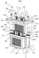
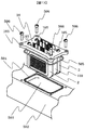
- FIG. 1 is an external perspective view of an assembly 10 in which a plurality of power semiconductor modules of this embodiment are assembled.
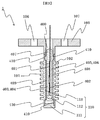
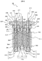
- FIG. 3 is an exploded perspective view of the assembly 10 disassembled. It is sectional drawing of the 1st power semiconductor module 1 seen from the arrow direction of the plane A of FIG. It is sectional drawing of the 2nd power semiconductor module 2 seen from the arrow direction of the plane B of FIG. It is sectional drawing of the assembly 10 seen from the arrow direction of the plane C of FIG.
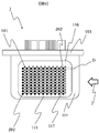
- FIG. 4 is a side view of the first power semiconductor module 1 with only the fins 202 of the second power semiconductor module 2 left.
- FIG. 3 is a side view of the first power semiconductor module 1 with only the fins 202 of the second power semiconductor module 2 left when the second power semiconductor module 2 is assembled.
- FIG. 4 is an external perspective view of the other surface side of the semiconductor cooling unit 400.
- FIG. FIG. 6 is an external perspective view of the semiconductor cooling unit 400 with the sealing resin 407 removed.
- FIG. 11 is an external perspective view in which a conductor portion 404 and a conductor portion 403 in FIG. 10 are removed.
- It is a circuit diagram which shows an example of the circuit structure incorporated in the semiconductor unit 400 of this embodiment.
- 5 is an external perspective view showing a process of assembling the assembly 10 to the flow path forming body 502.
- FIG. 2 is a cross-sectional view of the assembly 10 incorporated in a flow path forming body 502.
- FIG. 1 is an external perspective view of an assembly 10 in which a plurality of power semiconductor modules according to this embodiment are assembled.
- FIG. 2 is an exploded perspective view in which the assembly 10 is disassembled.
- the first power semiconductor module 1 has a first case 110 that houses a semiconductor unit 400 described later.
- the first case 110 forms an opening (not shown) through which a terminal extending from the semiconductor unit 30 passes.
- the first flange portion 103 is formed so as to surround the opening of the first case 110.
- the second power semiconductor module 2 has a second case 210 that houses the semiconductor unit 30.
- the second case 210 forms an opening 221 that allows a terminal extending from the semiconductor unit 400 to pass therethrough.
- the second flange portion 203 is formed so as to surround the opening 221.
- the third power semiconductor module 3 includes a third case 310 that houses the semiconductor unit 30.
- the third case 310 forms an opening 321 through which a terminal extending from the semiconductor unit 400 passes.
- the third flange portion 303 is formed so as to surround the opening 321.
- the through hole 106 is the first flange portion 103 and is formed in a region facing the opening 221 of the second power semiconductor module 2.
- the through hole 107 is the first flange portion 103 and is formed in a region facing the opening 321 of the third power semiconductor module 3.
- the through hole 104 a is formed on the side of one side of the through hole 106 in the short side direction
- the through hole 104 b is formed on the side of the other side of the through hole 106 in the short side direction.
- the through hole 108 a is formed on the side of one side of the through hole 107 in the short side direction, and the through hole 108 b is formed on the side of the other side of the through hole 107 in the short side direction.
- the second case 210 is formed with a connection portion 204a and a connection portion 204b connected to the fixture 105 such as a screw.
- the connecting portion 204a is formed on the side of one side of the opening 221 in the short side direction
- the connecting portion 204b is formed on the side of the other side of the opening 221 in the short side direction.
- the groove 205 When viewed from the direction perpendicular to the opening surface of the opening 221, the groove 205 is formed so as to surround the opening 221, the connecting portion 204 a, and the connecting portion 204 b.
- the seal member 206 is fitted into the groove portion 205.
- the third case 310 has a connection portion 304a (not shown) and a connection portion 304b connected to the fixture 105.
- the connecting portion 304a is formed on the side of one side of the opening 321 in the short side direction
- the connecting portion 304b is formed on the side of the other side of the opening 321 in the short side direction.
- the groove part 305 When viewed from the direction perpendicular to the opening surface of the opening part 321, the groove part 305 is formed so as to surround the opening part 321, the connection part 304a, and the connection part 304b.
- the seal member 306 is fitted into the groove portion 305.
- the second case 210 is connected to the first flange portion 103 by connecting the fixture 105 to the connection portion 204a and the connection portion 204b.
- the third case 310 is connected to the first flange portion 103 by connecting the fixture 105 to the connection portion 304a and the connection portion 304b.
- the third case 310 is disposed at a position facing the second case 210 with the first case 110 interposed therebetween.
- the first case 110 has the fins 101 on the surface formed toward the second case 210 and the fins 102 (see FIG. 3) on the surface formed toward the third case 310.
- the second case 210 has fins 202 (see FIG. 4) on the surface formed toward the first case 110, and the fins 201 on the surface opposite to the surface on which the first case 110 is disposed.
- the third case 310 has the fin 301 on the surface formed toward the first case 110, and the fin 302 (FIG. 5) on the surface opposite to the surface on which the first case 110 is disposed. See).
- FIG. 3 is a cross-sectional view of the first power semiconductor module 1 as seen from the direction of the arrow on the plane A in FIG.
- the semiconductor unit 400 includes a semiconductor element such as an IGBT 401 or a diode 402, conductor portions 403 to 406 connected to the IGBT 401 or the diode 402 via a solder material, and a sealing resin 407 for sealing the semiconductor element or the conductor portion.
- the first case 110 includes a frame body 111, a fin base portion 112, and a fin base portion 113.
- the frame body 111 forms two openings facing each other.
- the fin base 112 closes one opening of the frame 111.
- the fin base 113 closes the other opening of the frame 111.
- the semiconductor unit 400 is disposed in a space between the fin base portion 112 and the fin base portion 113.
- one surface of the semiconductor unit 400 is thermally connected to the fin base portion 112 via the insulating member 408.
- the other surface of the semiconductor unit 400 is thermally connected to the fin base portion 113 via the insulating member 409.
- the insulating members 408 and 409 are high heat conductive insulating layers, and use an insulating sheet or a sprayed film.
- the fin base portion 112 is formed integrally with the fin 102 and the fin base portion 113 is formed integrally with the fin 101 in order to improve the heat transfer coefficient.
- the fin base part 112 and the fin base part 113 are comprised, for example with aluminum, such as A1050 with favorable thermal conductivity.
- the fin base portion 112 and the fin base portion 113 are configured by a fin forming portion where the fin 101 and the fin 102 are formed, and an outer peripheral portion 410 surrounding the fin forming portion. And this outer peripheral part 410 is formed thinner than a fin formation part.
- the thin outer peripheral portion 410 adjusts the position of the fin forming portion to fix the semiconductor unit 400.
- the frame body 111 is formed of aluminum or the like having higher rigidity than the fin base portion 112 and the fin base portion 113 in order to improve the strength.
- the first flange portion 103 is formed in a direction perpendicular to the fin forming surface of the fin base portion 112. 4 is a cross-sectional view of the second power semiconductor module 2 as seen from the direction of the arrow on the plane B in FIG.
- the semiconductor unit 400 has the same structure and function as the semiconductor unit illustrated in FIG.
- the second case 210 includes a frame body 211, a fin base portion 212, and a fin base portion 213.
- the frame body 211 forms two openings facing each other.
- the fin base 212 closes one opening of the frame 211.
- the fin base portion 213 closes the other opening of the frame body 211.
- the semiconductor unit 400 is disposed in a space between the fin base portion 212 and the fin base portion 213. Furthermore, one surface of the semiconductor unit 400 is thermally connected to the fin base portion 212 via the insulating member 408. The other surface of the semiconductor unit 400 is thermally connected to the fin base portion 213 through the insulating member 409.
- the fin base portion 212 is formed integrally with the fins 202 and the fin base portion 213 is formed integrally with the fins 201 in order to improve the heat transfer coefficient.
- the fin base part 212 and the fin base part 213 are comprised with aluminum, such as A1050 with favorable heat conductivity, for example.
- the fin base portion 212 and the fin base portion 213 are configured by a fin forming portion where the fin 201 and the fin 202 are formed, and an outer peripheral portion 410 surrounding the fin forming portion. And this outer peripheral part 410 is formed thinner than a fin formation part. The thin outer peripheral portion 410 adjusts the position of the fin forming portion to fix the semiconductor unit 400.
- the frame body 211 is formed of aluminum or the like having higher rigidity than the fin base portion 212 and the fin base portion 213 in order to improve the strength.
- the second flange portion 203 is formed in a direction perpendicular to the fin forming surface of the fin base portion 212.
- the third case 310 is the same in structure and function as the second case 210, and thus the description thereof is omitted.
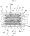
- 5 is a cross-sectional view of the assembly 10 as viewed from the direction of the arrow on the plane C in FIG.
- the second case 210 is connected to the first flange 103 so that the second case 210 forms a flow path space 500 for allowing the coolant to flow between the second case 210 and the first case 110.
- the flow rate of the refrigerant flowing through the flow path space 500 varies depending on the size of the vertical cross-sectional area of the flow path space 500 with respect to the flow direction of the refrigerant (the vertical direction of the paper surface of FIG. 5). As a result, the cooling performance of the first case 110 and the second case 210 changes. On the other hand, when it is attempted to improve the cooling performance by increasing the flow rate of the refrigerant by reducing the vertical sectional area of the flow path space 500, the second flange portion 103 of the first case 110 and the second flange portion 210 of the second case 210. The flange portion 203 interferes, and it may be difficult to adjust the flow rate of the refrigerant.
- first case 110 and the second case 210 are individually fixed to a fixing member (not shown in FIG. 5), the seal structure portion between the first case 110 and the fixing member, and the second case 210. And the sealing structure between the fixing member and the fixing member are provided in the upper part of the flow path space 500.
- the second case 210 is formed to be fixed to the first flange portion 103 of the first case 110 as in the present embodiment, and the first flange portion 103 supports the first case 110 and the second case 210. In this state, it is fixed to the fixing member.
- the number of seal structures in the upper part of the channel space 500 is reduced, and the cooling performance can be easily improved by adjusting the vertical sectional area of the channel space 500.
- it contributes to size reduction of the whole power converter device by miniaturizing the assembly 10 itself.
- the third case 310 is connected to the first flange 103 so that the third case 310 forms a flow path space 501 for allowing the coolant to flow between the third case 310 and the first case 110.
- the third case 310 is disposed opposite to the second case 210 with the first case 110 interposed therebetween, so that the first case 110 has a surface on the second case 210 side and a surface on the third case 310 side. Both sides can be efficiently cooled, and further downsizing of the entire power conversion device is promoted.
- the first case 110, the second case 210, and the third case 310 are used.
- the first case 110 and the second case 210 have the same effects.
- the seal members 206 and 306 made of an elastic member are used and the first case is crushed.
- the flange portion 103 is made watertight.
- the second case 210 and the third case 310 may be joined to the first flange portion 103 by welding or the like without using the seal members 206 and 306 formed of an elastic member.
- the insulating resin material 411 is filled in each case in a state where the semiconductor unit 400 is inserted into the first case 110, the second case 210, and the third case 310, respectively. Further, the insulating resin material 411 is also disposed in the through hole 106 and the through hole 107 of the first flange 103. That is, the insulating resin material 411 is disposed between the inner wall of the through hole 106 or the through hole 107 and the terminal. Thereby, it is possible to prevent the terminals extending from the second case 210 and the terminals extending from the third case 310 from coming into contact with the first flange 103, thereby improving insulation reliability and preventing breakage during assembly.
- the first case 110 is formed of a member different from the insulating resin material 411 and the sealing resin 407, but these may be integrated with the resin material or the like as the first case 110.
- the frame body 111 and the insulating resin material 411 may be an integral resin material
- the fin base portion 112 and the fin base portion 113 may be metal.
- the fin 101 is formed in the flow path space 500 such that the tip portion 114 of the fin 101 is closer to the fin base portion 212 than the connection portion 115 between the fin 101 and the fin base portion 113.
- FIG. 6 is a side view of the first power semiconductor module 1 with only the fins 202 of the second power semiconductor module 2 left. Fins 101 indicated by hatching are fins of the first power semiconductor module 1, and the fins 202 that are filled are fins of the second power semiconductor module 2.
- FIG. 6 is a side view of the first power semiconductor module 1 with only the fins 202 of the second power semiconductor module 2 left. Fins 101 indicated by hatching are fins of the first power semiconductor module 1, and the fins 202 that are filled are fins of the second power semiconductor module 2.
- FIG. 7 is a side view of the first power semiconductor module 1 in which only the fins 202 of the second power semiconductor module 2 are left when the second power semiconductor module 2 is assembled.
- Arrow F indicates the flow direction of the refrigerant.
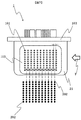
- the fin 101 includes a first row fin group 116 arranged in a direction crossing the refrigerant flow direction F.
- the fin 202 is formed so that the width of the fin 202 facing the refrigerant flow direction F is larger than the distance D between adjacent fins constituting the first row fin group 116. Further, when projected from the refrigerant flow direction F, the fins 202 are arranged such that the projected portions of the fins 202 overlap between adjacent fins constituting the first row fin group 116 (see FIG. 5).
- the fin 101 includes a second row fin group 117 arranged in a direction crossing the refrigerant flow direction F.
- the distance L between the second row fin group 117 and the first row fin group 116 in the refrigerant flow direction F is greater than the width of the fin 202 along the refrigerant flow direction F. Is also arranged to be larger.
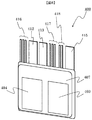
- FIG. 8 is an external perspective view of one surface side of the semiconductor cooling unit 400 of the present embodiment.
- FIG. 9 is an external perspective view of the other surface side of the semiconductor cooling unit 400.
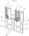
- FIG. 10 is an external perspective view of the semiconductor cooling unit 400 with the sealing resin 407 removed.
- FIG. 11 is an external perspective view in which the conductor portion 404 and the conductor portion 403 of FIG. 10 are further removed.
- the conductor portion 403 and the conductor portion 404 are arranged so that their main surfaces overlap each other on the virtual same plane.
- the conductor portion 405 and the conductor portion 406 are arranged so that their main surfaces overlap on a virtual same plane.
- a part of each main surface of the conductor part 403 and the conductor part 404 is exposed from the sealing resin 407 to form a heat dissipation surface.
- a part of each main surface of the conductor portion 405 and the conductor portion 406 is exposed from the sealing resin 407 to form a heat dissipation surface.
- the DC positive terminal 412 is connected to the conductor portion 406 and protrudes from the sealing resin 407.
- the DC negative terminal 413 is connected to the conductor portion 403 and protrudes from the sealing resin 407.
- the AC terminal 415 is connected to the conductor portion 405 and protrudes from the sealing resin 407.
- the upper arm side gate terminal 416 is connected to the gate electrode of the IGBT 401 constituting the upper arm circuit via the bonding wire 419.
- the lower arm side gate terminal 417 is connected to the gate electrode of the IGBT 401 constituting the lower arm circuit via the bonding wire 419.
- the temperature signal terminal 418 is connected to the temperature element via the bonding wire 419.
- the IGBT 401 and the diode 402 are respectively joined to the conductor portions 403 to 406 via a metal joining material.
- the metal bonding material for example, a solder material, a silver sheet, and a low-temperature sintered bonding material containing fine metal particles are used.
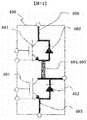
- FIG. 12 is a circuit diagram showing an example of a circuit configuration built in the semiconductor unit 400 of the present embodiment.
- the circuit shown in FIG. 12 shows a circuit configuration for one phase of the inverter circuit.
- a power transistor made of IBGT insulated gate bipolar transistor
- the conductor part 405 is connected to the collector electrode of the IGBT 401 on the upper arm side and the cathode electrode of the diode 402 on the upper arm side.
- the conductor plate 404 is connected to the collector electrode of the lower arm side IGBT 401 and the cathode electrode of the lower arm side diode 402.
- the assembly 10 shown in FIG. 1 is configured by forming one inverter circuit by providing the U-phase, V-phase, and W-phase for the semiconductor unit 400 configured as described above.
- the power conversion apparatus 100 according to the present embodiment is equipped with such an assembly 10 and has a small size and excellent cooling performance. Therefore, the vehicle drive electric machine of the in-vehicle electric system mounted on the electric vehicle or the hybrid vehicle is used. Can be used in the system.
- FIG. 13 is an external perspective view showing a process of assembling the assembly 10 to the flow path forming body 502.
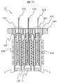
- FIG. 14 is a cross-sectional view of the assembly 10 incorporated in the flow path forming body 502.
- the flow path forming body 502 forms a flow path 507 for flowing a refrigerant that is mainly a liquid, and an opening 503 connected to the flow path 507.
- the groove portion 504 is formed so as to surround the opening 503, and the seal member 505 is fitted into the groove portion 504.
- the assembly 10 is fixed to the flow path forming body 502 by a fixture 506 in a state where the first flange portion 103 supports the first case 110, the second power semiconductor module 2, and the third power semiconductor module 3.
- the flow path forming body 502 functions as a fixing member.
- the first power semiconductor module 1, the second power semiconductor module 2, and the third power semiconductor module 3 are accommodated in the flow path 507 by closing the opening 503 with the first flange 103.
- the flow path 507 is formed so as to provide a flow path space 508 at a position facing the flow path space 500 with the second power semiconductor module 2 interposed therebetween.
- the second power semiconductor module 2 can be cooled from both sides of the flow path space 500 and the flow path space 508, and the outside of the first case 110 and the second case 210 can be directly cooled. , Cooling performance can be improved.
- at least two of the first power semiconductor module 1 and the second power semiconductor module 2 need not be separately attached to the flow path forming body 502 with watertightness.
- the seal between the flow path forming bodies 502 can be reduced from two places to one place, and downsizing can be promoted.
- the wall thickness of the flow path forming body 502 can also be used as part of the seal width. I can do it.
- the semiconductor modules can be arranged in parallel to ensure water tightness, and the power semiconductor modules can be arranged adjacent to each other. Therefore, when mounting a plurality of power semiconductor modules, the area to be mounted can be reduced in size. .
- the flow path 507 is formed so as to provide a flow path space 509 at a position facing the flow path space 501 with the third power semiconductor module 3 interposed therebetween.
- the third power semiconductor module 3 can be cooled from both sides of the flow path space 501 and the flow path space 509, and the outside of the first case 110 and the third case 310 can be directly cooled. , Cooling performance can be improved.
- Heat generated from the IGBT 401 and the diode 402 of the semiconductor unit 400 is conducted in the order of the conductor portions 403 to 406, the insulating members 408 and 409, the fin base portion 112, and the like, and is heated from the fin 101 and the like.
- the refrigerant is not allowed to flow to a portion where it is not necessary to cool, but to the fin formation region such as the fin 101.
- the flow path 507 forms recesses 510 to 512 at the bottom.
- the recess 510 is formed so that the side surface and the bottom surface of the first case 110 in which the fin 101 and the fin 102 are not formed are accommodated.
- the recess 511 is formed so that the side surface and the bottom surface of the second case 210 in which the fin 201 and the fin 202 are not formed are accommodated.
- the recess 512 is formed so that the side surface and the bottom surface of the third case 310 in which the fin 301 and the fin 302 are not formed are accommodated.
- the first power semiconductor module 1 is arranged at a position higher than the other second power semiconductor modules 2 and the third power semiconductor modules 3 at the bottom of the recess 510, the bottom of the other recess 511 and the recess 512 It is formed at a position higher than the bottom. Further, between the fin 101 and the second flange portion 203, a flow suppressing member 513 made of rubber or the like that does not damage other members is disposed. Further, the flow suppressing member 513 is disposed between the fin 201 and the second flange portion 203, between the fin 102 and the third flange portion 303, and between the fin 302 and the third flange portion 303.
- FIG. 15 is a cross-sectional view of a power converter according to another embodiment when a plane passing through the alternate long and short dash line in FIG. 14 is viewed from the direction of the arrow.
- the same configuration as the drawing number shown in FIGS. 1 to 14 has the same effect.
- it demonstrates centering on a different part from the power converter device demonstrated by FIG. 1 thru
- the fin 101 and the fin 202 overlap with each other in the flow direction of the refrigerant, so that the flow path space along the flow direction of the refrigerant.
- the cross-sectional area of 500 is smaller than the cross-sectional area of the flow path space 508 along the refrigerant flow direction.
- the flow path forming body 502 is a flow path space 508 and has a protruding portion 514 that protrudes toward the second case 210. .
- the cooling performance of the 2nd power semiconductor module 2 can be improved, and it contributes to size reduction of a power converter.
- the protrusion 514 is arranged so that the projection of the protrusion 514 overlaps with the projection of the power semiconductor element 401.
- FIG. 16 is a cross-sectional view of a power converter according to another embodiment when a plane passing through the alternate long and short dash line in FIG. 14 is viewed from the arrow direction.
- the same configuration as the drawing number shown in FIGS. 1 to 14 has the same effect.
- it demonstrates centering on a different part from the power converter device demonstrated by FIG. 1 thru
- the second case 210 includes fins 202 disposed in the flow path space 500 and fins 201 disposed in the flow path space 508.
- the first case 110 does not form fins in the flow path space 500.
- the fin 202 of the second power semiconductor module 2 is formed so that the front end thereof protrudes toward the first case 110 of the first power semiconductor module 1, and the front end of the fin 202 and the first case 110 are formed.
- the third case 310 has a fin 301 disposed in the flow path space 501 and a fin 302 disposed in the flow path space 509.
- the first case 110 does not form fins in the flow path space 501.
- the first case 110 includes the fins 2 disposed in the flow path space 500 and the fins disposed in the flow path space 501, while the second case 210.
- FIG. 17 is a cross-sectional view showing a state in which the assembly 11 according to another embodiment is incorporated in the flow path forming body 502.
- the same configuration as the drawing number shown in FIGS. 1 to 14 has the same effect. Here, it demonstrates centering on a different part from the power converter device demonstrated by FIG. 1 thru
- the second case 210 forms an opening 221 for projecting the positive DC terminal 412 and the like outside the second case 210
- the third case 310 projects the positive DC terminal 412 and the like outside the third case 310.
- the opening 321 is formed.
- the 1st flange part 103 forms the through-hole 118 in which the part which forms the opening part 221 of the 2nd case 210 is fitted, and the through-hole 119 in which the part which forms the opening part 321 of the 3rd case 310 is fitted.
- the positive DC terminal 412 and the like protrude to the side opposite to the side where the second power semiconductor module 2 and the third power semiconductor module 3 are disposed with the through hole 118 and the through hole 119 interposed therebetween. Therefore, the terminals of the second power semiconductor module 2 and the terminals of the third power semiconductor module 3 can suppress interference with the first flange portion 103, and can improve insulation reliability and assemblability.
- FIG. 18 is a cross-sectional view of a power conversion device according to another embodiment.
- the fins 102 disposed between the first case 110 of the first power semiconductor module 1 and the third case 310 of the third power semiconductor module 3 partially overlap in the axial direction of the fins 301 (the protruding direction of the fins). In other words, when viewed from the refrigerant flow direction F, the fins 102 and the fins 301 overlap.
- the overlapping length of the fins 102 and the fins 301 is about 2 / 3Y.
- the fin 302 is substantially the same as the length Y.
- the fin 102, the fin 301, and the fin 302 have the same length.
- the fin 102 and the fin 301 of the first power semiconductor module 1 and the third power semiconductor module 3 are connected to the other power semiconductor module.
- a 1 / 3Y gap is generated. Accordingly, since there are two channel cross-sectional areas, S1 and S2, in the part that does not overlap, a total of 2/3 of the cross-sectional area of the channel space 509 can be secured.
- the overlapping length of the fin 102 and the fin 301 is 2/3 of the fin total length Y, but the fin density of the flow path space 501 is twice as large as the fin density of the flow path space 509. Is equivalent to half of one third. Therefore, the channel cross-sectional areas of the channel space 501 and the channel space 509 are the same, the refrigerant can be flowed in a well-balanced manner, and heat dissipation with little variation can be ensured.
Landscapes
- Engineering & Computer Science (AREA)
- Microelectronics & Electronic Packaging (AREA)
- Physics & Mathematics (AREA)
- Thermal Sciences (AREA)
- Power Engineering (AREA)
- Inverter Devices (AREA)
Abstract
Description
図1は、本実施形態のパワー半導体モジュールを複数組み立てたアッセンブリ10の外観斜視図である。図2は、アッセンブリ10を分解した分解斜視図である。
第2パワー半導体モジュール2は、半導体ユニット30を収納する第2ケース210を有する。第2ケース210は、半導体ユニット400から延びる端子を貫通させる開口部221を形成する。第2フランジ部203は、開口部221を囲むように形成される。
第3パワー半導体モジュール3は、半導体ユニット30を収納する第3ケース310を有する。第3ケース310は、半導体ユニット400から延びる端子を貫通させる開口部321を形成する。第3フランジ部303は、開口部321を囲むように形成される。 貫通孔106は、第1フランジ部103であって、第2パワー半導体モジュール2の開口部221と対向する領域に形成される。貫通孔107は、第1フランジ部103であって、第3パワー半導体モジュール3の開口部321と対向する領域に形成される。さらに貫通孔104aは貫通孔106の短手方向の一方の辺の側部に形成され、貫通孔104bは貫通孔106の短手方向の他方の辺の側部に形成される。貫通孔108aは貫通孔107の短手方向の一方の辺の側部に形成され、貫通孔108bは貫通孔107の短手方向の他方の辺の側部に形成される。
第2ケース210は、ネジ等の固定具105と接続される接続部204a及び接続部204bが形成される。接続部204aは開口部221の短手方向の一方の辺の側部に形成され、接続部204bは開口部221の短手方向の他方の辺の側部に形成される。開口部221の開口面の垂直方向から見た場合、溝部205は、開口部221と接続部204a及び接続部204bを囲むように形成される。シール部材206は、溝部205に嵌め込まれる。
同様に、第3ケース310は、固定具105と接続される接続部304a(不図示)及び接続部304bが形成される。接続部304aは開口部321の短手方向の一方の辺の側部に形成され、接続部304bは開口部321の短手方向の他方の辺の側部に形成される。開口部321の開口面の垂直方向から見た場合、溝部305は、開口部321と接続部304a及び接続部304bを囲むように形成される。シール部材306は、溝部305に嵌め込まれる。
第2ケース210は、固定具105が接続部204a及び接続部204bに接続されることにより、第1フランジ部103に接続される。同様に第3ケース310は、固定具105が接続部304a及び接続部304bに接続されることにより、第1フランジ部103に接続される。第3ケース310は、第1ケース110を挟んで第2ケース210と対向する位置に配置される。
第1ケース110は、第2ケース210に向かって形成された面にフィン101を有し、かつ第3ケース310に向かって形成された面にフィン102(図3参照)を有する。第2ケース210は、第1ケース110に向かって形成された面にフィン202 (図4参照)を有し、かつ第1ケース110が配置された側の面とは反対側の面にフィン201を有する。同様に第3ケース310は、第1ケース110に向かって形成された面にフィン301 を有し、かつ第1ケース110が配置された側の面とは反対側の面にフィン302 (図5参照)を有する。
図3は、図2の平面Aの矢印方向から見た第1パワー半導体モジュール1の断面図である。
半導体ユニット400は、IGBT401やダイオード402の半導体素子と、IGBT401やダイオード402と半田材を介して接続される導体部403ないし406と、半導体素子や導体部を封止する封止樹脂407と、を有する。半導体ユニット400の詳細構造については、図8ないし図12にて説示する。
第1ケース110は、枠体111とフィンベース部112とフィンベース部113とにより構成される。枠体111は、互いに対向する2つの開口部を形成する。フィンベース部112は、枠体111の一方の開口部を塞ぐ。フィンベース部113は、枠体111の他方の開口部を塞ぐ。
半導体ユニット400は、フィンベース部112とフィンベース部113との間の空間に配置される。さらに半導体ユニット400の一方の面は、絶縁部材408を介してフィンベース部112と熱的に接続される。半導体ユニット400の他方の面は、絶縁部材409を介してフィンベース部113と熱的に接続される。絶縁部材408及び409は、高熱伝導性の絶縁層であり、絶縁シートを用いたり、溶射膜を用いたりする。
本実施形態においては、熱伝達率を向上させるために、フィンベース部112はフィン102と一体に形成され、フィンベース部113はフィン101と一体に形成される。また、フィンベース部112とフィンベース部113は、例えば、熱伝導性が良好なA1050等のアルミニウムにより構成される。
また、フィンベース部112及びフィンベース部113は、フィン101やフィン102が形成されるフィン形成部と、このフィン形成部を囲む外周部410とにより構成される。そして、この外周部410は、フィン形成部よりも薄く形成される。この薄く形成された外周部410は、フィン形成部の位置を調整して半導体ユニット400を固定する。
枠体111は、強度を向上させるために、フィンベース部112及びフィンベース部113よりも剛性が高いアルミニウム等で形成される。第1フランジ部103は、フィンベース部112のフィン形成面に対して垂直方向に形成される。
図4は、図2の平面Bの矢印方向から見た第2パワー半導体モジュール2の断面図である。
半導体ユニット400は、図3にて説示した半導体ユニットと構造及び機能が同一のため説明を省略する。
第2ケース210は、枠体211とフィンベース部212とフィンベース部213とにより構成される。枠体211は、互いに対向する2つの開口部を形成する。フィンベース部212は、枠体211の一方の開口部を塞ぐ。フィンベース部213は、枠体211の他方の開口部を塞ぐ。
半導体ユニット400は、フィンベース部212とフィンベース部213との間の空間に配置される。さらに半導体ユニット400の一方の面は、絶縁部材408を介してフィンベース部212と熱的に接続される。半導体ユニット400の他方の面は、絶縁部材409を介してフィンベース部213と熱的に接続される。
本実施形態においては、熱伝達率を向上させるために、フィンベース部212はフィン202と一体に形成され、フィンベース部213はフィン201と一体に形成される。また、フィンベース部212とフィンベース部213は、例えば、熱伝導性が良好なA1050等のアルミニウムにより構成される。
また、フィンベース部212及びフィンベース部213は、フィン201やフィン202が形成されるフィン形成部と、このフィン形成部を囲む外周部410とにより構成される。そして、この外周部410は、フィン形成部よりも薄く形成される。この薄く形成された外周部410は、フィン形成部の位置を調整して半導体ユニット400を固定する。
枠体211は、強度を向上させるために、フィンベース部212及びフィンベース部213よりも剛性が高いアルミニウム等で形成される。第2フランジ部203は、フィンベース部212のフィン形成面に対して垂直方向に形成される。
なお、第3ケース310は、第2ケース210と構造及び機能において同一なので、説明を省略する。
図5は、図1の平面Cの矢印方向から見たアッセンブリ10の断面図である。
第2ケース210は、この第2ケース210が第1ケース110との間に冷媒を流すための流路空間500を形成するように、第1フランジ103に接続される。この流路空間500に流れる冷媒の流速は、冷媒の流れ方向(図5の紙面の垂直方向)に対する流路空間500の垂直断面積の大きさによって変化する。それにより、第1ケース110及び第2ケース210の冷却性能が変化する。
一方、流路空間500の垂直断面積を小さくすることにより冷媒の流速を増加させて冷却性能を向上させようとした場合、第1ケース110の第1フランジ部103と第2ケース210の第2フランジ部203が干渉してしまい、冷媒の流速の調整が困難となるおそれがある。つまり、第1ケース110と第2ケース210がそれぞれ個別に固定部材(図5では不図示)に固定される場合、第1ケース110と固定部材との間のシール構造部と、第2ケース210と固定部材との間のシール構造部とのそれぞれが流路空間500 の上部に設けられることになる。
なお、本実施形態では、第1ケース110は、絶縁性樹脂材411や封止樹脂407とは別の部材で構成されているが、これらを樹脂材料等により一体として第1ケース110としてもよい。例えば、枠体111と絶縁性樹脂材411を一体の樹脂材料として、フィンベース部112やフィンベース部113を金属としてよい。第2ケース210や第3ケース310についても同様である。
また、フィン101は、流路空間500において、このフィン101の先端部114がフィン101とフィンベース部113との接続部115よりもフィンベース部212に近づくように形成される。さらにフィン201は、流路空間500において、このフィン201の先端部214がフィン201とフィンベース部212との接続部215よりもフィンベース部113に近づくように形成される。これにより、第1ケース110と第2ケース210の冷却性能を向上させるとともに小型化を促進することができる。なお、流路空間501における、フィン102及びフィン302も同様な関係と作用効果を奏する。
図6は、第2パワー半導体モジュール2のフィン202のみを残した第1パワー半導体モジュール1の側面図である。斜線部で示したフィン101が第1パワー半導体モジュール1のフィンであり、塗り潰されたフィン202が第2パワー半導体モジュール2のフィンである。図7は、第2パワー半導体モジュール2を組み付時における、第2パワー半導体モジュール2のフィン202のみを残した第1パワー半導体モジュール1の側面図である。
矢印Fは、冷媒の流れ方向を示す。フィン101は、冷媒の流れ方向Fを横切る方向に並べられた第1列フィン群116を含んで構成される。そしてフィン202は、冷媒の流れ方向Fと対向する当該フィン202の幅が第1列フィン群116を構成する隣り合うフィンの間の距離Dよりも大きくなるように形成される。さらに冷媒の流れ方向Fから投影した場合、フィン202は、当該フィン202の射影部が第1列フィン群116を構成する隣り合うフィンの間に重なるように配置される(図5参照)。 これにより、フィン101とフィン202との間に流れる冷媒は、冷媒の流れ方向に対して効率良く流されることになり、冷却性能が向上する。なお、流路空間501における、フィン102及びフィン301も同様な関係と作用効果を奏する。
また、フィン101は、冷媒の流れ方向Fを横切る方向に並べられた第2列フィン群117を含んで構成される。そして、第2列フィン群117は、冷媒の流れ方向Fにおける当該第2列フィン群117と第1列フィン群116との間の距離Lが冷媒の流れ方向Fに沿ったフィン202の幅よりも大きくなるように配置される。これにより、第2ケース210が第1フランジ部103に接続される際の挿入方向は、冷媒の流れ方向Fを横切る方向である場合、接続部の位置決めや固定具105による固定作業時に、フィン101とフィン202が干渉することを避けることができ、冷却性能を維持しながら、生産性を向上させることができる。
図8は、本実施形態の半導体冷却ユニット400の一方の面側の外観斜視図である。図9は、半導体冷却ユニット400の他方の面側の外観斜視図である。図10は、半導体冷却ユニット400の封止樹脂407を除去した外観斜視図である。図11は、さらに図10の導体部404及び導体部403を取り除いた外観斜視図である。
図10に図示されるように、導体部403と導体部404はそれぞれの主面が仮想同一面上に重なるように配置される。導体部405と導体部406はそれぞれの主面が仮想同一面上に重なるように配置される。図8に図示されるように、導体部403と導体部404のそれぞれの主面の一部が封止樹脂407から露出して放熱面を形成する。同様に図9に図示されるように、導体部405と導体部406のそれぞれの主面の一部が封止樹脂407から露出して放熱面を形成する。
直流正極端子412は、導体部406と接続され、かつ封止樹脂407から突出する。直流負極端子413は、導体部403と接続され、かつ封止樹脂407から突出する。交流端子415は、導体部405と接続され、かつ封止樹脂407から突出する。上アーム側ゲート端子416は、ボンディングワイヤ419を介して、上アーム回路を構成するIGBT401のゲート電極と接続される。下アーム側ゲート端子417は、ボンディングワイヤ419を介して、下アーム回路を構成するIGBT401のゲート電極と接続される。温度信号端子418は、ボンディングワイヤ419を介して、温度素子と接続される。
IGBT401やダイオード402は、導体部403ないし406に、金属接合材を介してそれぞれ接合される。金属接合材としては、例えば、半田材や銀シート及び微細金属粒子を含んだ低温焼結接合材等を用いる。
図12は、本実施形態の半導体ユニット400に内蔵される回路構成の一例を示す回路図である。図12に図示された回路は、インバータ回路の1相分の回路構成を示す。
図13は、アッセンブリ10を流路形成体502に組み付ける工程を示した外観斜視図である。図14は、流路形成体502に組み込まれたアッセンブリ10の断面図である。
流路形成体502は、主に液体である冷媒を流すための流路507と、この流路507と繋がる開口503と、を形成する。溝部504は、開口503を囲むように形成され、この溝部504にシール部材505が嵌め込まれる。
アッセンブリ10は、第1フランジ部103が第1ケース110と第2パワー半導体モジュール2と第3パワー半導体モジュール3を支持した状態で、固定具506によって流路形成体502に固定される。ここで流路形成体502は、固定部材として機能する。
これにより、第1パワー半導体モジュール1と第2パワー半導体モジュール2と第3パワー半導体モジュール3は、第1フランジ103で開口503を塞ぐことにより、流路507に収納される。
図14に示されるように、流路507は、第2パワー半導体モジュール2を挟んで流路空間500と対向する位置に流路空間508を設けるように形成される。これにより、第2パワー半導体モジュール2は、流路空間500と流路空間508の両側から冷却することができ、かつ第1ケース110と第2ケース210の外側を直接冷却することができるために、冷却性能を向上させることができる。
言い換えると、本実施形態により、少なくとも二つの、第1パワー半導体モジュール1と第2パワー半導体モジュール2を、流路形成体502に別々に水密性をもたせ取付ける必要がないことから、パワー半導体モジュールと流路形成体502間のシールは、二箇所から一箇所に減らせることができ、小型化を促進させることができる。
また、第1パワー半導体モジュール1の第1フランジ部103のフランジ面に別のパワー半導体モジュールを流路側から取付けることから、流路形成体502の壁部厚さもシール巾の一部として用いることが出来る。このようにして半導体モジュールを並列に配置し水密性を確保した上でパワー半導体モジュール同士を隣接して配置出来ることから複数のパワー半導体モジュールを搭載する際、搭載する領域を小形化することが出来る。
また、図14に示されるように、流路507は、第3パワー半導体モジュール3を挟んで流路空間501と対向する位置に流路空間509を設けるように形成される。これにより、第3パワー半導体モジュール3は、流路空間501と流路空間509の両側から冷却することができ、かつ第1ケース110と第3ケース310の外側を直接冷却することができるために、冷却性能を向上させることができる。
また、半導体ユニット400のIGBT401,ダイオード402から発生した熱は、導体部403ないし406、絶縁部材408や409、フィンベース部112等の順に伝導し、フィン101等から熱される。放熱効率を向上させる為に、冷媒は冷却する必要性がない部位に流さないようにして、フィン101等のフィン形成領域に流すようにする。そこで、流路507は、その底部に凹部510ないし512を形成する。具体的には、凹部510は、フィン101及びフィン102が形成されていない第1ケース110の側面及び底面が収納されるように形成される。凹部511は、フィン201及びフィン202が形成されていない第2ケース210の側面及び底面が収納されるように形成される。凹部512は、フィン301及びフィン302が形成されていない第3ケース310の側面及び底面が収納されるように形成される。凹部510の底部は、第1パワー半導体モジュール1が他の第2パワー半導体モジュール2や第3パワー半導体モジュール3よりも高い位置に配置されていることから、他の凹部511の底部と凹部512の底部よりも高い位置に形成される。また、フィン101と第2フランジ部203との間には、他の部材に破損を与えないようなゴム等により構成された流れ抑制部材513が配置される。またフィン201と第2フランジ部203との間、フィン102と第3フランジ部303との間、フィン302と第3フランジ部303との間、のそれぞれに、流れ抑制部材513が配置される。これにより、冷媒はフィン形成領域に流れ易くなり、冷却性能を向上させることができる。
図15は、図14の一点鎖線を通る平面を矢印方向から見た他の実施形態に係る電力変換装置の断面図である。図1ないし図14にて示した図面番号と同じ構成は同様の作用効果を奏する。ここでは、図1ないし図14で説示された電力変換装置とは異なる部分を中心に説明する。
第1パワー半導体モジュール1と第2パワー半導体モジュール2との間に設けられる流路空間500は冷媒の流れ方向に対してフィン101とフィン202が重なり合うので、冷媒の流れ方向に沿った流路空間500の断面積が、冷媒の流れ方向に沿った流路空間508の断面積よりも小さくなる。流路空間500と流路空間508の冷媒流量を平衡化させるために、そこで、流路形成体502は、流路空間508であって、第2ケース210に向かって突出する突出部514を有する。これにより、第2パワー半導体モジュール2の冷却性能を向上させることができるとともに電力変換装置の小型化に寄与する。
また、パワー半導体素子401の電極面と垂直方向Pから投影した場合、突出部514は、突出部514の射影部がパワー半導体素子401の射影部と重なるように配置される。これにより、発熱体であるパワー半導体素子401の近傍で冷媒の流速を速め、放熱性を向上させることができる。
なお、流路空間509側に設けられた突出部515についても、上記と同様の作用効果を奏する。
図16は、図14の一点鎖線を通る平面を矢印方向から見た他の実施形態に係る電力変換装置の断面図である。図1ないし図14にて示した図面番号と同じ構成は同様の作用効果を奏する。ここでは、図1ないし図14で説示された電力変換装置とは異なる部分を中心に説明する。
第2ケース210は、流路空間500に配置されるフィン202と流路空間508に配置されるフィン201を有する。一方、第1ケース110は、流路空間500に、フィンを形成しない。これにより、流路空間500と流路空間508に流れる冷媒流量は平衡化するようになり、各パワー半導体モジュールにおいてばらつきの少ない放熱性を確保出来る。また、第2パワー半導体モジュール2のフィン202は、その先端部が第1パワー半導体モジュール1の第1ケース110に向かって突出するように形成され、フィン202の先端部と第1ケース110との間において流路が絞られ冷媒の流速が増すことから、放熱面積の減少による放熱性への影響を小さくすることが出来る。
同様に、第3ケース310は、流路空間501に配置されるフィン301と流路空間509に配置されるフィン302を有する。一方、第1ケース110は、流路空間501に、フィンを形成しない。これにより上記と同様に作用効果を奏する。
なお、上記と同様の作用効果を奏する構造として、第1ケース110は、流路空間500に配置されるフィン2と流路空間501に配置されるフィンを有して、一方、第2ケース210は流路空間500にフィンを形成しないようにし、第3ケース310は流路空間501にフィンを形成しないように構成してよい。
図17は、他の実施形態に係るアッセンブリ11を流路形成体502に組み込んだ状態を示す断面図である。図1ないし図14にて示した図面番号と同じ構成は同様の作用効果を奏する。ここでは、図1ないし図14で説示された電力変換装置とは異なる部分を中心に説明する。
第2ケース210は正極直流端子412等を第2ケース210の外部に突出させるための開口部221を形成し、第3ケース310は正極直流端子412等を第3ケース310の外部に突出させるための開口部321を形成する。そして、第1フランジ部103は、第2ケース210の開口部221を形成する部分が嵌め込まれる貫通孔118を形成するとともに、第3ケース310の開口部321を形成する部分が嵌め込まれる貫通孔119を形成する。これにより正極直流端子412等は、貫通孔118や貫通孔119を挟んで第2パワー半導体モジュール2や第3パワー半導体モジュール3が配置された側とは反対側に突出することになる。よって、第2パワー半導体モジュール2の端子や第3パワー半導体モジュール3の端子は、第1フランジ部103との干渉を抑制することができ、絶縁信頼性や組立性を向上させることができる。また第1パワー半導体モジュール1と第2パワー半導体モジュール2と第3パワー半導体モジュール3のそれぞれの端子の先端の高さを揃えることができたり、第1パワー半導体モジュール1と第2パワー半導体モジュール2と第3パワー半導体モジュール3の底面の位置を揃えることができたりし、小型化や組立性を向上させることができる。なお、第1フランジ部103と第2ケース210は水密性が有り熱変形の小さい接合方法、例えばレーザー溶接等により接続される。
図18は、他の実施形態に係る電力変換装置の断面図である。第1パワー半導体モジュール1の第1ケース110と第3パワー半導体モジュール3の第3ケース310の間に配置されるフィン102とフィン301の軸方向(フィンの突出方向)で一部重なり合う。言い換えると冷媒の流れ方向Fから見たときにフィン102とフィン301が重なり合う。
このような構成により、第1パワー半導体モジュール1と第3パワー半導体モジュール3の夫々のフィン102及びフィン301は、他方のパワー半導体モジュールに対して、1/3Yの隙間が生じる。これより、重なり合わない部位の流路断面積は、S1とS2の2箇所ある為、流路空間509に対し合計2/3の流路断面積を確保出来る。また、フィン102とフィン301の重なり合う長さは、フィン全長Yの2/3あるが、流路空間501のフィン密度は流路空間509のフィン密度よりも2倍大きくなる為、流路断面積は、半分の1/3相当となる。よって、流路空間501と流路空間509の流路断面積は同一となり、冷媒をバランスよく流すことができ、ばらつきの少ない放熱性を確保出来る。
Claims (13)
- 第1パワー半導体モジュールと、第2半導体モジュールと、前記第1パワー半導体モジュールを固定する固定部材と、を備える電力変換装置であって、
前記第1パワー半導体モジュールは、第1パワー半導体素子と、当該第1パワー半導体素子を収納する第1ケースと、当該ケースに接続される第1フランジ部と、を有し、
前記第2パワー半導体モジュールは、第2パワー半導体素子と、当該第2パワー半導体素子を収納する第2ケースと、を有し、
前記第2ケースは、当該第2ケースが前記第1ケースとの間に冷媒を流すための第1流路空間を設けるように、前記第1フランジ部に接続され、
前記第1フランジ部は、前記第1ケース及び前記第2パワー半導体モジュールを支持した状態で前記固定部材に固定される電力変換装置。 - 請求項1に記載された電力変換装置であって、
第3パワー半導体素子と当該第2パワー半導体素子を収納する第3ケースを有する第3パワー半導体モジュールを備え、
前記第3ケースは、前記第1ケースを挟んで前記第2ケースと対向して配置され、
さらに前記第3ケースは、当該第3ケースが前記第1ケースとの間に冷媒を流すための第2流路空間を設けるように、前記第1フランジ部に接続され、
前記第1フランジ部は、前記第1ケース及び前記第3パワー半導体モジュールを支持した状態で前記固定部材に固定される電力変換装置。 - 請求項1または2に記載された電力変換装置であって、
前記固定部材は、冷媒を流すための流路を形成する流路形成体であり、
前記流路形成体は、前記流路と繋がる開口を形成し、
前記第1パワー半導体モジュール及び前記第2パワー半導体モジュールは、前記第1フランジで前記開口を塞ぐことにより、前記流路に収納され、
前記流路は、前記第2パワー半導体モジュールを挟んで前記第1流路空間と対向する位置に第2流路空間を設けるように形成される電力変換装置。 - 請求項1または2に記載された電力変換装置であって、
前記第2パワー半導体モジュールは、前記第2パワー半導体素子に流す電流又は制御信号を伝達するための端子を有し、
前記第2ケースは、前記端子を当該第2ケースの外部に突出させるための開口部を形成し、
前記第1フランジ部は、前記端子を貫通させるための貫通孔を形成し、
前記貫通孔の内壁と前記端子との間には、絶縁性樹脂材が配置される電力変換装置。 - 請求項1ないし4に記載のいずれかの電力変換装置において、
前記第1ケースは、第1フィンと、当該第1フィンと接続される第1フィンベースと、を有し、
前記第2ケースは、第2フィンと、当該第2フィンと接続される第2フィンベースと、を有し、
前記第1フィンは、前記第1流路空間において、当該第1フィンの先端部が当該第1フィンと前記第1フィンベースとの接続部よりも前記第2フィンベースに近づくように形成され、
前記第2フィンは、前記第1流路空間において、当該第2フィンの先端部が当該第2フィンと前記第2フィンベースとの接続部よりも前記第1フィンベースに近づくように形成される電力変換装置。 - 請求項5に記載の電力変換装置であって、
前記第1フィンは、冷媒の流れ方向を横切る方向に並べられた第1列フィン群を含んで構成され、
前記第2フィンは、冷媒の流れ方向と対向する当該第2フィンの幅が前記第1列フィン群を構成する隣り合うフィンの間の距離よりも大きくなるように形成され、
冷媒の流れ方向から投影した場合、前記第2フィンは、当該第2フィンの射影部が前記第1列フィン群を構成する隣り合うフィンの間に重なるように配置される電力変換装置。 - 請求項6に記載の電力変換装置であって、
前記第1フィンは、冷媒の流れ方向を横切る方向に並べられた第2列フィン群を含んで構成され、
前記第2列フィン群は、前記冷媒の流れ方向における当該第2列フィン群と前記第1列フィン群との間の距離が前記冷媒の流れ方向に沿った前記第2フィンの幅よりも大きくなるように配置され、
前記第2ケースが前記第1フランジ部に接続される際の挿入方向は、前記冷媒の流れ方向を横切る方向である電力変換装置。 - 請求項3に記載された電力変換装置であって、
前記第1ケースは、前記第1流路空間に配置される第1フィンを有し、
前記第2ケースは、前記第1流路空間と前記第2流路空間に分かれて配置される複数の第2フィンを有し、
前記流路形成体は、前記第2流路空間であって、当該第2ケースに向かって突出する突出部を有する電力変換装置。 - 請求項8に記載された電力変換装置であって、
前記第2パワー半導体素子の電極面と垂直方向から投影した場合、前記突出部は、当該突出部の射影部が前記第2パワー半導体素子の射影部と重なるように配置される電力変換装置。 - 請求項3に記載された電力変換装置であって、
前記第2ケースは、前記第1流路空間と前記第2流路空間に分かれて配置される複数のフィンを有し、
前記第1ケースは、前記第1流路空間に、フィンを形成しない電力変換装置。 - 請求項10に記載された電力変換装置であって、
第3パワー半導体素子と当該第3パワー半導体素子を収納する第3ケースを有する第3パワー半導体モジュールを備え、
前記第3ケースは、前記第1ケースを挟んで前記第2ケースと対向して配置され、
さらに前記第3ケースは、当該第3ケースが前記第1ケースとの間に冷媒を流すための第3流路空間を設けるように、前記第1フランジ部に接続され、
前記第1フランジ部は、前記第1ケース及び前記第3パワー半導体モジュールを支持した状態で前記流路形成体に固定され、
前記流路は、前記第3パワー半導体モジュールを挟んで前記第3流路空間と対向する位置に第4流路空間を設けるように形成され、
前記第3ケースは、前記第3流路空間と前記第4流路空間に分かれて配置される複数のフィンを有し、
前記第1ケースは、前記第3流路空間に、フィンを形成しない電力変換装置。 - 請求項3に記載された電力変換装置であって、
前記第1ケースは、前記第1流路空間に配置される第1フィンを有し、
前記第2ケースは、前記第2流路空間に配置される第2フィンを有し、
さらに前記第2ケースは、前記第1流路空間に、フィンを形成しない電力変換装置。 - 請求項1または2に記載された電力変換装置であって、
前記第2パワー半導体モジュールは、前記第2パワー半導体素子に流す電流又は制御信号を伝達するための端子を有し、
前記第2ケースは、前記端子を当該第2ケースの外部に突出させるための開口部を形成し、
前記第1フランジ部は、前記第2ケースの開口部を形成する部分が嵌め込まれる貫通孔を形成し、
前記端子は、前記貫通孔を挟んで前記第2パワー半導体モジュールが配置された側とは反対側に突出する電力変換装置。
Priority Applications (2)
| Application Number | Priority Date | Filing Date | Title |
|---|---|---|---|
| US15/025,364 US9992915B2 (en) | 2013-10-07 | 2014-10-01 | Power conversion device |
| JP2015541536A JP6161713B2 (ja) | 2013-10-07 | 2014-10-01 | 電力変換装置 |
Applications Claiming Priority (2)
| Application Number | Priority Date | Filing Date | Title |
|---|---|---|---|
| JP2013-209797 | 2013-10-07 | ||
| JP2013209797 | 2013-10-07 |
Publications (1)
| Publication Number | Publication Date |
|---|---|
| WO2015053140A1 true WO2015053140A1 (ja) | 2015-04-16 |
Family
ID=52812957
Family Applications (1)
| Application Number | Title | Priority Date | Filing Date |
|---|---|---|---|
| PCT/JP2014/076239 Ceased WO2015053140A1 (ja) | 2013-10-07 | 2014-10-01 | 電力変換装置 |
Country Status (3)
| Country | Link |
|---|---|
| US (1) | US9992915B2 (ja) |
| JP (1) | JP6161713B2 (ja) |
| WO (1) | WO2015053140A1 (ja) |
Cited By (5)
| Publication number | Priority date | Publication date | Assignee | Title |
|---|---|---|---|---|
| CN107863891A (zh) * | 2016-09-21 | 2018-03-30 | 本田技研工业株式会社 | 电力转换装置 |
| JP2018113343A (ja) * | 2017-01-12 | 2018-07-19 | 日立オートモティブシステムズ株式会社 | パワー半導体装置 |
| WO2021106519A1 (ja) * | 2019-11-27 | 2021-06-03 | 日立Astemo株式会社 | パワーモジュールおよびパワーモジュールの製造方法 |
| DE102016219070B4 (de) | 2015-10-09 | 2022-06-02 | Schaeffler Technologies AG & Co. KG | Gehäuse für ein Halbbrückenmodul und ein Verfahren zur Herstellung einer Kühlstruktur |
| DE112023006773T5 (de) | 2023-10-12 | 2026-07-23 | Fanuc Corporation | Motorantriebsvorrichtung |
Families Citing this family (7)
| Publication number | Priority date | Publication date | Assignee | Title |
|---|---|---|---|---|
| EP3101688B1 (en) * | 2014-01-27 | 2019-10-02 | Hitachi, Ltd. | Power module and manufacturing method therefor |
| US10607919B2 (en) * | 2017-04-28 | 2020-03-31 | Semiconductor Components Industries, Llc | Semiconductor package having junction cooling pipes embedded in substrates |
| USD906269S1 (en) * | 2019-08-28 | 2020-12-29 | Carbice Corporation | Flexible heat sink |
| USD904322S1 (en) * | 2019-08-28 | 2020-12-08 | Carbice Corporation | Flexible heat sink |
| USD903610S1 (en) * | 2019-08-28 | 2020-12-01 | Carbice Corporation | Flexible heat sink |
| CN114520200B (zh) * | 2022-02-28 | 2025-03-11 | 广东电网有限责任公司广州供电局 | 一种柔直换流阀功率模块用高强度绝缘挡板 |
| CN119547206B (zh) * | 2022-10-04 | 2026-05-19 | 华为技术有限公司 | 采用直接液冷的半导体结构 |
Citations (4)
| Publication number | Priority date | Publication date | Assignee | Title |
|---|---|---|---|---|
| JP2006202899A (ja) * | 2005-01-19 | 2006-08-03 | Toyota Motor Corp | 半導体冷却装置 |
| JP2008259267A (ja) * | 2007-04-02 | 2008-10-23 | Hitachi Ltd | インバータ回路用の半導体モジュール |
| JP2012016095A (ja) * | 2010-06-29 | 2012-01-19 | Denso Corp | 電力変換装置 |
| JP2012029539A (ja) * | 2010-07-28 | 2012-02-09 | Hitachi Automotive Systems Ltd | 電力変換装置 |
Family Cites Families (12)
| Publication number | Priority date | Publication date | Assignee | Title |
|---|---|---|---|---|
| JP4284625B2 (ja) * | 2005-06-22 | 2009-06-24 | 株式会社デンソー | 三相インバータ装置 |
| JP4580997B2 (ja) * | 2008-03-11 | 2010-11-17 | 日立オートモティブシステムズ株式会社 | 電力変換装置 |
| JP5557441B2 (ja) | 2008-10-31 | 2014-07-23 | 日立オートモティブシステムズ株式会社 | 電力変換装置および電動車両 |
| JP5557585B2 (ja) * | 2010-04-26 | 2014-07-23 | 日立オートモティブシステムズ株式会社 | パワーモジュール |
| JP5380376B2 (ja) * | 2010-06-21 | 2014-01-08 | 日立オートモティブシステムズ株式会社 | パワー半導体装置 |
| JP5273101B2 (ja) * | 2010-06-23 | 2013-08-28 | 株式会社デンソー | 半導体モジュールおよびその製造方法 |
| JP5417314B2 (ja) * | 2010-12-27 | 2014-02-12 | 日立オートモティブシステムズ株式会社 | 電力変換装置 |
| JP5591396B2 (ja) * | 2011-03-04 | 2014-09-17 | 日立オートモティブシステムズ株式会社 | 半導体モジュール、および半導体モジュールの製造方法 |
| JP5508357B2 (ja) * | 2011-07-29 | 2014-05-28 | 日立オートモティブシステムズ株式会社 | 電力変換装置 |
| JP5634429B2 (ja) * | 2012-03-30 | 2014-12-03 | 日立オートモティブシステムズ株式会社 | パワー半導体モジュール |
| JP5879233B2 (ja) * | 2012-08-31 | 2016-03-08 | 日立オートモティブシステムズ株式会社 | パワー半導体モジュール |
| JP5805838B1 (ja) * | 2014-09-29 | 2015-11-10 | 株式会社日立製作所 | 発熱体の冷却構造、電力変換器ユニットおよび電力変換装置 |
-
2014
- 2014-10-01 US US15/025,364 patent/US9992915B2/en active Active
- 2014-10-01 JP JP2015541536A patent/JP6161713B2/ja active Active
- 2014-10-01 WO PCT/JP2014/076239 patent/WO2015053140A1/ja not_active Ceased
Patent Citations (4)
| Publication number | Priority date | Publication date | Assignee | Title |
|---|---|---|---|---|
| JP2006202899A (ja) * | 2005-01-19 | 2006-08-03 | Toyota Motor Corp | 半導体冷却装置 |
| JP2008259267A (ja) * | 2007-04-02 | 2008-10-23 | Hitachi Ltd | インバータ回路用の半導体モジュール |
| JP2012016095A (ja) * | 2010-06-29 | 2012-01-19 | Denso Corp | 電力変換装置 |
| JP2012029539A (ja) * | 2010-07-28 | 2012-02-09 | Hitachi Automotive Systems Ltd | 電力変換装置 |
Cited By (8)
| Publication number | Priority date | Publication date | Assignee | Title |
|---|---|---|---|---|
| DE102016219070B4 (de) | 2015-10-09 | 2022-06-02 | Schaeffler Technologies AG & Co. KG | Gehäuse für ein Halbbrückenmodul und ein Verfahren zur Herstellung einer Kühlstruktur |
| CN107863891A (zh) * | 2016-09-21 | 2018-03-30 | 本田技研工业株式会社 | 电力转换装置 |
| US10284105B2 (en) * | 2016-09-21 | 2019-05-07 | Honda Motor Co., Ltd. | Power converter |
| CN107863891B (zh) * | 2016-09-21 | 2020-02-14 | 本田技研工业株式会社 | 电力转换装置 |
| JP2018113343A (ja) * | 2017-01-12 | 2018-07-19 | 日立オートモティブシステムズ株式会社 | パワー半導体装置 |
| WO2018131301A1 (ja) * | 2017-01-12 | 2018-07-19 | 日立オートモティブシステムズ株式会社 | パワー半導体装置 |
| WO2021106519A1 (ja) * | 2019-11-27 | 2021-06-03 | 日立Astemo株式会社 | パワーモジュールおよびパワーモジュールの製造方法 |
| DE112023006773T5 (de) | 2023-10-12 | 2026-07-23 | Fanuc Corporation | Motorantriebsvorrichtung |
Also Published As
| Publication number | Publication date |
|---|---|
| US20160234976A1 (en) | 2016-08-11 |
| JP6161713B2 (ja) | 2017-07-12 |
| JPWO2015053140A1 (ja) | 2017-03-09 |
| US9992915B2 (en) | 2018-06-05 |
Similar Documents
| Publication | Publication Date | Title |
|---|---|---|
| JP6161713B2 (ja) | 電力変換装置 | |
| JP5314933B2 (ja) | 電力変換装置 | |
| JP5957396B2 (ja) | 両面冷却型電力変換装置 | |
| JP6469720B2 (ja) | 電力変換装置 | |
| JP6296888B2 (ja) | 電力変換装置 | |
| US20160037654A1 (en) | Power Converter | |
| JP2010087002A (ja) | 発熱部品冷却構造 | |
| JP2005057130A (ja) | 半導体冷却ユニット | |
| WO2014061447A1 (ja) | 電力変換装置 | |
| CN101281904A (zh) | 逆变电路用的半导体模块 | |
| JP6899784B2 (ja) | パワー半導体装置 | |
| JP2015076932A (ja) | 電力変換装置 | |
| JP6101609B2 (ja) | パワー半導体モジュール及びそれを用いた電力変換装置 | |
| JP2020145285A (ja) | 半導体モジュールとそれを備えた半導体装置 | |
| WO2019003718A1 (ja) | パワー半導体装置及びそれを用いた電力変換装置 | |
| JP5409889B2 (ja) | インバータ | |
| JP5267238B2 (ja) | 半導体装置及び半導体装置の製造方法 | |
| US20250343105A1 (en) | Power conversion device | |
| JP7183373B1 (ja) | 電力変換装置 | |
| JP4935783B2 (ja) | 半導体装置および複合半導体装置 | |
| WO2013084417A1 (ja) | 電力変換装置 | |
| JP2018063999A (ja) | 半導体装置 | |
| JP2017108078A (ja) | 冷却器及びパワー半導体モジュール | |
| JP2014007209A (ja) | 半導体装置及びその製造方法 | |
| JP2015185835A (ja) | 半導体装置及びその製造方法 |
Legal Events
| Date | Code | Title | Description |
|---|---|---|---|
| 121 | Ep: the epo has been informed by wipo that ep was designated in this application |
Ref document number: 14852690 Country of ref document: EP Kind code of ref document: A1 |
|
| WWE | Wipo information: entry into national phase |
Ref document number: 15025364 Country of ref document: US |
|
| ENP | Entry into the national phase |
Ref document number: 2015541536 Country of ref document: JP Kind code of ref document: A |
|
| NENP | Non-entry into the national phase |
Ref country code: DE |
|
| 122 | Ep: pct application non-entry in european phase |
Ref document number: 14852690 Country of ref document: EP Kind code of ref document: A1 |