WO2015052999A1 - シフトレジスタ及び表示装置 - Google Patents
シフトレジスタ及び表示装置 Download PDFInfo
- Publication number
- WO2015052999A1 WO2015052999A1 PCT/JP2014/072121 JP2014072121W WO2015052999A1 WO 2015052999 A1 WO2015052999 A1 WO 2015052999A1 JP 2014072121 W JP2014072121 W JP 2014072121W WO 2015052999 A1 WO2015052999 A1 WO 2015052999A1
- Authority
- WO
- WIPO (PCT)
- Prior art keywords
- signal
- shift register
- thin film
- gate
- film transistor
- Prior art date
- Legal status (The legal status is an assumption and is not a legal conclusion. Google has not performed a legal analysis and makes no representation as to the accuracy of the status listed.)
- Ceased
Links
Images










Classifications
-
- G—PHYSICS
- G09—EDUCATION; CRYPTOGRAPHY; DISPLAY; ADVERTISING; SEALS
- G09G—ARRANGEMENTS OR CIRCUITS FOR CONTROL OF INDICATING DEVICES USING STATIC MEANS TO PRESENT VARIABLE INFORMATION
- G09G3/00—Control arrangements or circuits, of interest only in connection with visual indicators other than cathode-ray tubes
- G09G3/20—Control arrangements or circuits, of interest only in connection with visual indicators other than cathode-ray tubes for presentation of an assembly of a number of characters, e.g. a page, by composing the assembly by combination of individual elements arranged in a matrix no fixed position being assigned to or needed to be assigned to the individual characters or partial characters
- G09G3/34—Control arrangements or circuits, of interest only in connection with visual indicators other than cathode-ray tubes for presentation of an assembly of a number of characters, e.g. a page, by composing the assembly by combination of individual elements arranged in a matrix no fixed position being assigned to or needed to be assigned to the individual characters or partial characters by control of light from an independent source
- G09G3/36—Control arrangements or circuits, of interest only in connection with visual indicators other than cathode-ray tubes for presentation of an assembly of a number of characters, e.g. a page, by composing the assembly by combination of individual elements arranged in a matrix no fixed position being assigned to or needed to be assigned to the individual characters or partial characters by control of light from an independent source using liquid crystals
- G09G3/3611—Control of matrices with row and column drivers
- G09G3/3674—Details of drivers for scan electrodes
- G09G3/3677—Details of drivers for scan electrodes suitable for active matrices only
-
- G—PHYSICS
- G11—INFORMATION STORAGE
- G11C—STATIC STORES
- G11C19/00—Digital stores in which the information is moved stepwise, e.g. shift registers
- G11C19/28—Digital stores in which the information is moved stepwise, e.g. shift registers using semiconductor elements
-
- G—PHYSICS
- G09—EDUCATION; CRYPTOGRAPHY; DISPLAY; ADVERTISING; SEALS
- G09G—ARRANGEMENTS OR CIRCUITS FOR CONTROL OF INDICATING DEVICES USING STATIC MEANS TO PRESENT VARIABLE INFORMATION
- G09G2300/00—Aspects of the constitution of display devices
- G09G2300/08—Active matrix structure, i.e. with use of active elements, inclusive of non-linear two terminal elements, in the pixels together with light emitting or modulating elements
- G09G2300/0809—Several active elements per pixel in active matrix panels
- G09G2300/0814—Several active elements per pixel in active matrix panels used for selection purposes, e.g. logical AND for partial update
-
- G—PHYSICS
- G09—EDUCATION; CRYPTOGRAPHY; DISPLAY; ADVERTISING; SEALS
- G09G—ARRANGEMENTS OR CIRCUITS FOR CONTROL OF INDICATING DEVICES USING STATIC MEANS TO PRESENT VARIABLE INFORMATION
- G09G2310/00—Command of the display device
- G09G2310/02—Addressing, scanning or driving the display screen or processing steps related thereto
- G09G2310/0264—Details of driving circuits
- G09G2310/0286—Details of a shift registers arranged for use in a driving circuit
Definitions
- the present invention relates to a shift register and a display device, and more particularly to a shift register used for a drive circuit of a display device.
- peripherals such as a pixel thin film transistor (Thin FilmThTransistor) for injecting charges into a pixel and a drive circuit for driving a scanning line or a signal line connected to the pixel thin film transistor
- Thin FilmThTransistor pixel thin film transistor
- a so-called monolithic circuit technique in which a thin film transistor for a peripheral circuit constituting a circuit is formed on the same glass substrate has become widespread.
- a scanning line driving circuit selects display elements arranged in a two-dimensional form in units of rows, and writes a voltage corresponding to display data to the selected display elements, thereby displaying an image. Yes.
- a shift register that sequentially shifts output signals based on a clock signal is used as the scanning line drive circuit.
- a similar shift register is provided inside a signal line driver circuit for driving signal lines.
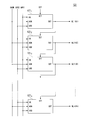
- FIG. 22 is a diagram showing a configuration example of a shift register according to the prior art disclosed in International Publication No. 2012/0297799.
- the shift register shown in the figure is configured by cascade-connecting multiple stages of shift register unit circuits SRU1, SRU2, SRU3,..., SRUn (n is a natural number of 2 or more).
- Each of the shift register unit circuits SRU1, SRU2, SRU3,..., SRUn is supplied with clock signals CK1, CK2 and all-on control signals AON, AONB (AONB is an inverted signal of AON).
- the start pulse signal ST is input to the set terminal SET of the first-stage shift register unit circuit SRU1, and the previous stage shift is set to each set terminal SET of the second-stage and subsequent shift register unit circuits SRU2, SRU3,.
- the output terminal OUT of the register unit circuit is connected.
- the output terminals OUT of the shift register unit circuits SRU1, SRU2, SRU3,..., SRUn are connected to the scanning lines GL1, GL2, GL3,.
- Each of the shift register unit circuits SRU1, SRU2, SRU3,..., SRUn has the same configuration, and hereinafter refers to any one of the shift register unit circuits SRU1, SRU2, SRU3,. Sometimes referred to as “shift register unit circuit SRU”.
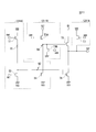
- FIG. 23 is a diagram showing a configuration example of the shift register unit circuit SRU according to the prior art shown in FIG.
- the shift register unit circuit SRU includes n-channel MOS (MetalMetaOxide Semiconductor) field effect transistors (hereinafter referred to as “NMOS transistors”) Q1 to Q9, a resistor R1, and capacitors CA and CB.
- MOS MetalMetaOxide Semiconductor field effect transistors
- the NMOS transistors Q5, Q6, Q7, the resistor R1, and the capacitor CB constitute an inactive output control unit SRUA
- the NMOS transistors Q1, Q4, Q8 constitute an active output control unit SRUB
- the NMOS transistors Q2, Q2 Q9 and capacitor CA constitute an active output unit SRUC
- NMOS transistor Q3 constitutes an inactive output unit SRUD.
- the active output control unit SRUB controls the active output unit SRUC to set the output signal to a high level
- the inactive output control unit SRUA controls the inactive output unit SRUD to set the output signal to a low level.
- the clock signal CK1 and the clock signal CK2 are input to the clock terminal CK and the clock terminal CKB of the odd stage shift register unit circuit SRU, respectively.
- the clock signal CK2 and the clock signal CK1 are input to the clock terminal CK and the clock terminal CKB of the even-numbered shift register unit circuit SRU, as opposed to the odd-numbered shift register unit circuit.
- the clock signal CK1 and the clock signal CK2 are clock signals whose phases are shifted from each other by 180 °, for example, and a low level section of each signal is set so as not to be at a high level at the same time.
- phase difference between the clock signal CK1 and the clock signal CK2 is not limited to 180 °, and the clock signal CK1 and the clock signal CK2 are arbitrary clock signals as long as the high-level periods do not overlap each other. It can be.
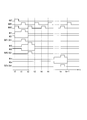
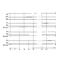
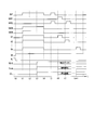
- FIG. 24A and 24B are time charts for explaining an example of the operation of the shift register according to the prior art
- FIG. 24A is a time chart during normal operation
- FIG. 24B is a time chart during all-on operation.
- the high level and low level of the start pulse signal ST and the clock signals CK1 and CK2 correspond to the power supply voltage VDD and the ground voltage VSS supplied to the shift register, respectively.
- N11 and N21 represent nodes N1 and N2 of the first-stage shift register unit circuit SRU1
- N12 and N22 represent nodes N1 and N2 of the second-stage shift register unit circuit SRU2.
- N1n, N2n represent nodes N1, N2 of the n-th shift register unit circuit SRUn, and OUT1, OUT2, OUTn represent output signals of the first-stage, second-stage, and n-th shift register unit circuit SRU. ing.
- the all-on control signal AON is set to a low level
- the all-on control signal AONB which is an inverted signal thereof, is set to a high level.
- the start pulse signal ST is input to the set terminal SET of the first-stage shift register unit circuit SRU1 at time t0
- the NMOS transistor Q1 is turned on in the active output control unit SRUB, and the node N11 is connected to the NMOS from the power supply voltage VDD.
- the transistor Q1 is precharged to a voltage (VDD ⁇ Vth) dropped by the threshold voltage Vth.
- the clock signal CK2 input to the clock terminal CKB and the start pulse signal ST input to the set terminal SET are both at a high level, so that the NMOS transistors Q5, Q6, Q7 All are turned on, but since the resistance R1 is high resistance, the voltage of the node N21 becomes a low level near the ground voltage VSS. As a result, the signal level of the gates of the NMOS transistors Q3 and Q4 becomes low level, and both the NMOS transistors Q3 and Q4 are turned off.
- the source voltage of the NMOS transistor Q2 increases.
- the source voltage of the NMOS transistor Q2 rises, the voltage at the node N11 is pushed up to a voltage higher than the power supply voltage VDD due to the bootstrap effect by the capacitor CA.
- the gate voltage of the NMOS transistor Q2 becomes high, the NMOS transistor Q2 transmits the high level of the clock signal CK1 input to the clock terminal CK to the output terminal OUT1 without causing a voltage drop due to the threshold voltage Vth.
- the output signal OUT1 is activated at a high level.
- the NMOS transistor Q5 is turned on, thereby increasing the voltage at the node N21.
- the gate voltages of the NMOS transistor Q3 and NMOS transistor Q4 rise, and both the NMOS transistor Q3 and NMOS transistor Q4 are turned on to simultaneously discharge the node N11 and pull down the output terminal OUT.
- the output signal OUT1 becomes low level and deactivated.
- the NMOS transistor Q5 is turned on, whereby the signal level of the node N21 is maintained at a high level.
- the NMOS transistors Q3 and Q4 are both kept on, and the output signal OUT1 is kept at the low level.
- next-stage shift register unit circuit SRU2 the output signal of the output terminal OUT1 of the first-stage shift register unit circuit SRU1 is input to the set terminal SET of the second-stage shift register unit circuit SRU2.
- the node N12 is precharged.
- the output signal OUT2 is output from the output terminal OUT of the second-stage shift register unit circuit SRU2.
- time t3 when the clock signal CK1 transitions to a high level, the node N12 in the second-stage shift register unit circuit SRU2 is simultaneously discharged and the output terminal OUT is pulled down, so that the output signal OUT2 becomes a low level. Deactivated.
- the plurality of shift register unit circuits SRU1, SRU2, SRU3,..., SRUn perform a shift operation and sequentially output high-level pulse signals to the scanning lines GL1, GL2, GL3,.
- a stable shift operation can be performed using only the two-phase clock signals CK1 and CK2 and the output signal of the previous stage as input signals without generating a through current.
- the all-on control signal AON is set to a high level
- the all-on control signal AONB which is an inverted signal thereof, is set to a low level.
- the start pulse signal ST and the clock signals CK1 and CK2 are both set to a high level.
- the NMOS transistor Q9 When the all-on control signal AON is set to the high level and the all-on control signal AONB is set to the low level, the NMOS transistor Q9 is turned on and the NMOS transistor Q8 is turned off in the first-stage shift register unit circuit SRU1. Become. In this case, since the NMOS transistor Q6 is turned off and the NMOS transistor Q7 is turned on, the node N21 is at a low level (ground voltage VSS), and the NMOS transistor Q3 whose gate is connected to the node N21 is turned off. As a result, there is no element that drives the output terminal OUT to a low level. When the NMOS transistor Q9 is turned on in such a state, a high level output signal OUT1 is output to the output terminal OUT.
- the thin film transistor Q8 is turned off together with the NMOS transistor Q6. Thereby, the through current in the active output control unit SRUB is cut off.
- the NMOS transistor Q6 is turned off, the signal level of the node N2 is set to a low level by the NMOS transistor Q7 based on the signal input to the set terminal SET.
- the NMOS transistor Q3 whose gate is connected to the node N2 is turned off, so that a through current flowing through the NMOS transistors Q2 and Q3 is also prevented.
- the number of transistors in the shift register is increased because the NMOS transistors Q6 and Q8 are provided in order to prevent a through current during all-on operation.
- the NMOS transistor Q1 and the NMOS transistor Q8 are connected in series, when the node N1 is charged, the charge voltage of the node N1 is lowered due to the threshold voltage Vth, the on-resistance, and the like of the NMOS transistor Q1 and the NMOS transistor Q8.
- One embodiment of the present invention has been made in view of the above problems, and an object thereof is to provide a shift register capable of reducing the number of transistors and a display device including the shift register.
- a shift register is a shift register in which a plurality of unit circuits are cascade-connected, and the unit circuit has a current path between a clock terminal to which a first clock signal is applied and an output terminal.
- the first output transistor connected, the second output transistor having a current path connected between the output terminal and a predetermined potential node, and the signal levels of the output signals of the plurality of unit circuits are set to a predetermined signal level.
- a setting unit that sets a signal level of the output terminal to the predetermined signal level when the control signal for active is active, and the first output in response to the control signal when the control signal is active
- the second clock signal following the first clock signal, or the first clock signal A first output control unit that turns on the first output transistor by supplying an input signal to the control electrode of the first output transistor in response to a predetermined signal; and when the control signal is active, the second output A second output that turns off the first output transistor and turns on the second output transistor in response to a second clock signal following the first clock signal when the transistor is turned off and the control signal is inactive.
- a shift register having a control unit.
- the number of transistors included in the shift register can be reduced.
- FIG. 1 is a schematic block diagram showing a configuration example of a display device 100 according to the first embodiment of the present invention.
- the display device 100 is, for example, an active matrix liquid crystal display device, and includes a display unit 110, a scanning line driving circuit (gate driver) 120, a signal line driving circuit (source driver) 130, a display control circuit 140, a power supply circuit 150, a signal.
- Line selection thin film transistors (analog switches) TS1, TS2,..., TSm, and other circuits are provided.
- the display unit 110 includes a plurality of signal lines SL1, SL2,..., SLm (m: natural number) arranged to extend in the vertical line direction and a plurality of signal lines arranged to extend in the horizontal line direction. Scanning lines GL1, GL2,... GLn (n: natural number) and a plurality of pixel portions PIX.
- the plurality of pixel portions PIX are arranged in a matrix so as to be located at the intersections of the signal lines SL1, SL2,..., SLm and the scanning lines GL1, GL2,. .
- Each of the plurality of pixel portions PIX is formed by a liquid crystal (liquid crystal material) LC disposed between two substrates, a pixel thin film transistor TC provided on one substrate, and the liquid crystal LC.
- a pixel capacitor portion (auxiliary capacitor) CS and a counter electrode (transparent electrode) Tcom provided on the other substrate are provided.
- the pixel thin film transistor TC has a gate connected to the scanning line GLp (p: 1 ⁇ p ⁇ n) passing through the above-described intersection, and the signal line SLq (q: 1 ⁇ q ⁇ m) (Integer) is connected to the source, and the drain is connected to the first terminal of the pixel capacitor portion CS.
- the pixel capacitor unit CS holds a voltage corresponding to each pixel value (gradation value) based on a data signal for displaying a video (image) on the display device 100.
- the second terminal of the pixel capacitor portion CS is connected to the auxiliary capacitor electrode line CSL.
- the auxiliary capacitance electrode line CSL is provided assuming a VA (Vertical Alignment) method.
- the present invention is not limited to this example, and the present invention includes an IPS (In Plane Switching) method and the like.
- the second electrode of the pixel capacitor portion CS may be connected to the counter electrode Tcom.
- the pixel thin film transistor TC is an n-channel field effect transistor.
- the pixel thin film transistor TC is not limited to an n-channel thin film transistor, and any type of transistor can be used.
- the scanning line driving circuit 120 includes a shift register 121.
- the shift register 121 sequentially supplies scanning signals (gate signals G1, G2,... Gn described later) to the scanning lines GL1, GL2,. To do.
- the pixel unit PIX is driven in units of horizontal lines.
- the shift register 121 sequentially shifts the gate start pulse signal GST in synchronization with the gate clock signals GCK1 and GCK2, so that the scanning signal is transmitted to the scanning lines GL1 and GL2 at a predetermined time interval. ,..., GLn.
- the scanning line driving circuit 120 applies the scanning lines GL1, GL2,... GLn to the scanning lines GL1, GL2,.
- the scanning line driving circuit 120 is composed of a peripheral circuit thin film transistor formed on the same glass substrate as the pixel thin film transistor TC described above.
- the peripheral circuit thin film transistor is an n-channel field effect transistor, as is the pixel thin film transistor TC.
- the signal line driving circuit 130 includes a shift register 131.
- the signal line driving circuit 130 sequentially selects the signal line selection thin film transistors TS1, TS2,..., TSm by sequentially shifting the source start pulse signal SST in synchronization with the source clock signals SCK1 and SCK2.
- a data signal VSIG for supplying a voltage corresponding to a pixel value (gradation value) to each pixel unit PIX is output to the signal lines SL1, SL2,..., SLm via the line selection thin film transistors TS1, TS2,. .
- the signal line driving circuit 130 applies the data signal VSIG for one horizontal line to each pixel via the signal lines SL1, SL2,..., SLm selected by the signal line selection thin film transistors TS1, TS2,. To the part PIX.
- the signal line driving circuit 130 selects all of the signal lines SL1, SL2,..., SLm by the signal line selection thin film transistors TS1, TS2,. It has a function of setting to a high level (predetermined signal level).
- the signal line driving circuit 130 includes a peripheral circuit thin film transistor formed on the same glass substrate as the pixel thin film transistor TC.
- the scanning line driving circuit 120 and the signal line driving circuit 130 are formed on the same glass substrate as the pixel thin film transistor TC.
- the present invention is not limited to this example.
- Only the driving circuit 120 may be formed on the same glass substrate as the pixel thin film transistor TC, and a data signal may be supplied from an external IC (Integrated Circuit) having the function of the signal line driving circuit 130. .
- only the signal line driver circuit 130 may be formed on the same glass substrate as the pixel thin film transistor TC, and the scanning line driver circuit 120 may be provided outside.
- the display control circuit 140 generates various control signals necessary for displaying an image on the display unit 110 and supplies the control signals to the scanning line driving circuit 120 and the signal line driving circuit 130.
- the display control circuit 140 generates a control signal for causing the display unit 110 to display an image during the image display period, and supplies the control signal to the scanning line driving circuit 120 and the signal line driving circuit 130.
- the display control circuit 140 includes the gate clock signals GCK1 and GCK2, the source clock signals SCK1 and SCK2, the gate start pulse signal GST, the source start pulse signal SST, the gate full on control signal GAON, and the source full on control signal SAON, A data signal VSIG and the like are generated.
- the power supply circuit 150 is for supplying operating power supply voltages (VDD, VH, VL, etc.) of the scanning line driving circuit 120 and the signal line driving circuit 130.
- a capacitor C120 is formed in the power supply wiring between the power supply circuit 150 and the scanning line driving circuit 120, and a capacitor C130 is formed in the power supply wiring between the power supply circuit 150 and the signal line driving circuit 130.
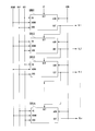
- FIG. 2 is a schematic block diagram illustrating a configuration example of the shift register 121 according to the first embodiment.
- the shift register 121 includes a plurality of shift register unit circuits 121 1 , 121 2 , 121 3 ,..., 121 n corresponding to the plurality of scanning lines GL1, GL2, GL3,. Yes.
- the plurality of shift register unit circuits 121 1 , 121 2 , 121 3 ,..., 121 n are connected in cascade.
- Each of the plurality of shift register unit circuits 121 1 , 121 2 , 121 3 ,..., 121 n has the same configuration, and hereinafter, the shift register unit circuits 121 1 , 121 2 , 121 3 , .., 121 n are collectively referred to as “shift register unit circuit 1211”.
- the shift register unit circuit 1211 includes clock terminals CK and CKB, a set terminal SET, an output terminal OUT, and an all-on control terminal AON.
- the gate clock signal GCK1 is input to the clock terminal CK of the odd-stage shift register unit circuit, and the gate clock is input to the clock terminal CKB.
- the signal GCK2 is input.
- the gate clock signal GCK2 is input to the clock terminal CK of the even-numbered shift register unit circuit, and the gate clock signal GCK1 is input to the clock terminal CKB.
- a plurality of shift register unit circuits 121 1, 121 2, 121 3, ..., the all-on control terminal AON of 121 n gate all-on control signal GAON is input.
- the gate start pulse signal GST is input to the set terminal SET of the first stage shift register unit circuit 121 1 , and the second and subsequent stages The output signal of the preceding shift register unit circuit is input to each set terminal SET of the shift register unit circuit.
- the shift register unit circuits 121 1 in a plurality of stages, 121 2, 121 3, ..., the shift register 121 is composed of 121 n receives the gate start pulse signal GST from the display control circuit 140, a gate clock signal GCK1, GCK2 Based on this, a shift operation is performed, and gate signals G1, G2, G3,..., Gn are sequentially output to the scanning lines GL1, GL2, GL3,.
- the phase of the gate clock signal GCK1 and the phase of the gate clock signal GCK2 are different from each other by 180 degrees as shown in FIGS. 4A and 4B described later.
- the low level interval is set so that the gate clock signal GCK1 and the gate clock signal GCK2 do not simultaneously become high level.
- the phase difference between the gate clock signal GCK1 and the gate clock signal GCK2 is not limited to 180 °, and the clock signal CK1 and the clock signal CK2 can be set to any clock as long as the high-level periods do not overlap each other. It can be a signal. Further, depending on the logic (positive logic / negative logic) of the gate clock signal GCK1 and the gate clock signal GCK2, each signal level in the non-overlapping period can be arbitrary. The same applies to the source clock signals SCK1 and SCK2.
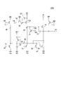
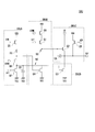
- FIG. 3 is a circuit diagram showing a configuration example of the shift register unit circuit 1211 in the first embodiment.
- the shift register unit circuit 1211 includes thin film transistors T1, T2, T3A, T3B, T4, T5, T6, and T7, which are n-channel field effect transistors, and a resistor R1.
- the thin film transistor T1 is supplied with the power supply voltage VDD at its drain, and its gate is connected to the clock terminal CKB.
- a gate clock signal GCK2 is input to the clock terminal CKB.
- the thin film transistor T1 outputs a voltage that is lowered by the threshold voltage Vth of the thin film transistor T1 from the source with reference to the gate voltage.
- the resistor R1 has one end connected to the source of the thin film transistor T1 and the other end connected to the drain of the thin film transistor T2.
- the resistance value of the resistor R1 is set to a high value so that the drain voltage of the thin film transistor T2 is low enough to turn off the thin film transistors T4 and T6 in a state where both the thin film transistors T1 and T2 are turned on.
- the arrangement position of the resistor R1 and the arrangement position of the thin film transistor T1 may be interchanged.
- the power supply voltage VDD may be applied to one end of the resistor R1
- the drain of the thin film transistor T1 may be connected to the other end of the resistor R1
- the drain of the thin film transistor T2 may be connected to the source of the thin film transistor T1.
- the thin film transistor T2 has its source connected to the ground node (predetermined potential node) and its gate connected to the set terminal SET.
- a gate start pulse signal GST or an output signal of the preceding shift register unit circuit is input to the set terminal SET.
- the gate start pulse signal GST is input to the first stage of the shift register unit circuit 121 1 of the set terminal SET, 2-stage and subsequent shift register unit circuit 121 2, 121 3, ..., 121 n set terminal of The SET is supplied with the output signal of the preceding shift register unit circuit.
- the thin film transistor T2 is turned on when a signal input to the set terminal SET becomes high level, and outputs a low level corresponding to the ground voltage VSS from its drain.
- the drain of the thin film transistor T3A is connected to a set terminal SET to which an input signal is applied, its gate is connected to a clock terminal CKB to which a gate clock signal GCK2 is applied, and its source is connected to the drain of the thin film transistor T4.
- the thin film transistor T3A has a threshold voltage of the thin film transistor T3A based on the gate voltage. A voltage dropped by Vth is output from the source.
- a gate of the thin film transistor T5 is connected to a connection point between the source of the thin film transistor T3A and the drain of the thin film transistor T4.
- connection point between the source of the thin film transistor T3A and the drain of the thin film transistor T4 is connected to the drain of the thin film transistor T3B, the source of the thin film transistor T3B is connected to the ground node (VSS), and the gate of the thin film transistor T3B It is connected to an all-on control terminal AON to which an on-control signal GAON is given.
- the drain of the thin film transistor T4 is connected to the source of the thin film transistor T3A, the gate is connected to the connection point between the drain of the thin film transistor T2 and the resistor R1, and the source is connected to the ground node.
- the thin film transistor T4 is turned on when the signal level at the connection point between the thin film transistor T2 and the resistor R1 becomes a high level, and outputs a low level corresponding to the ground voltage VSS from its drain.
- the thin film transistor T5 (first output transistor) has its drain connected to the clock terminal CK, its gate connected to a connection point between the source of the thin film transistor T3A and the drain of the thin film transistor T4, and its source connected to the output terminal OUT.
- a gate clock signal GCK1 is input to the clock terminal CK.
- the thin film transistor T5 has the signal level of the gate clock signal GCK1 input to the clock terminal CK at the output terminal OUT when the signal level at the connection point between the source of the thin film transistor T3A and the drain of the thin film transistor T4 becomes high level. To transmit.
- the high level of the gate clock signal GCK1 does not cause a voltage drop due to the threshold voltage Vth of the thin film transistor T5.
- the output terminal OUT To the output terminal OUT.
- the thin film transistor T6 (second output transistor) has its drain connected to the output terminal OUT, its gate connected to the connection point between the drain of the thin film transistor T2 and the resistor R1, and its source connected to the ground node. Yes.
- the thin film transistor T6 is turned on when the signal level at the connection point between the drain of the thin film transistor T2 and the resistor R1 becomes a high level, and outputs a low level corresponding to the ground voltage VSS from the drain to the output terminal OUT. .
- the thin film transistor T7 has its drain supplied with the power supply voltage VDD, its gate connected to the all-on control terminal AON, and its source connected to the output terminal OUT.
- a gate all-on control signal GAON is input to the all-on control terminal AON.
- the thin film transistor T7 has a threshold voltage of the thin film transistor T7 based on the gate voltage (high level of the gate all-on control signal GAON).
- a voltage dropped by Vth is output from the source to the output terminal OUT.
- the thin film transistor T7 may be provided in the form of a so-called diode connection. Specifically, the gate of the thin film transistor T7 may be connected to the drain, the source thereof may be connected to the output terminal OUT, and the gate all-on control signal AON may be input to the connection point between the gate and the drain of the thin film transistor T7.
- the connection point between the source of the thin film transistor T3A and the drain of the thin film transistor T4 forms a node N1
- the connection point between the resistor R1 and the drain of the thin film transistor T2 forms a node N2.
- the thin film transistor T5 constitutes a first output transistor in which a current path is connected between the clock terminal CK to which the clock signal CK1 is applied and the output terminal OUT.
- the thin film transistor T6 constitutes a second output transistor in which a current path is connected between the output terminal OUT and a ground node (predetermined potential node).
- the thin film transistor T7 has an all-on control terminal AON for setting the signal level of the output signals of the plurality of shift register unit circuits 121 1 , 121 2 , 121 3 ,..., 121 n to a high level (predetermined signal level).
- the setting unit 1211A is configured to set the signal level of the output terminal OUT to a high level (predetermined signal level).
- the thin film transistors T3A and T3B turn off the thin film transistor T5 in response to the gate all-on control signal GAON, and the gate all-on control signal GAON is not.
- the input signal of the set terminal SET is supplied to the control electrode of the thin film transistor T5, and the thin film output transistor T5 is
- the first output control unit 1211B to be turned on is configured. In the example of FIG.
- the first output control unit 1211B when the gate all-on control signal GAON is inactive, receives the input signal of the set terminal SET in response to the gate clock signal GCK2 input to the clock terminal CKB. It supplies to the control electrode of T5. However, when the gate all-on control signal GAON is inactive, the first output control unit 1211B controls the input signal of the thin film transistor T5 in response to a signal synchronized with either the gate clock signal GCK2 or the gate clock signal GCK1. You may supply to an electrode.
- the thin film transistor T3A functions as a setting unit that sets the signal level of the node N1 when the gate full-on control signal GAON is inactive.
- the thin film transistor T3B functions as a discharge circuit that discharges the node N1 when the gate full-on control signal GAON is active.
- the thin film transistors T1, T2, T4 and the resistor R1 turn off the thin film transistor T6 when the gate full-on control signal GAON input to the full-on control terminal AON is active, and the gate full-on control signal GAON is inactive.
- the second output control unit 1211C is configured to turn off the thin film transistor T5 and turn on the thin film transistor T6 in response to the gate clock signal GCK2 following the gate clock signal GCK1 or a signal synchronized with the gate clock signal GCK1.
- the display control circuit 140 generates the gate clock signal GCK1 and the gate clock signal GCK2 and supplies them to the scanning line driving circuit 120. However, one clock supplied to the scanning line driving circuit 120 is used.
- the gate clock signal GCK1 and the gate clock signal GCK2 may be derived from the signals in the scanning line driver circuit 120.
- the above-mentioned “signal synchronized with the gate clock signal GCK1” is a signal corresponding to the gate clock signal GCK2 when the scanning line driving circuit 120 is derived from one clock signal together with the gate clock signal GCK1. That is, the generation method of the gate clock signal GCK1 and the gate clock signal GCK2 is arbitrary, and may be generated outside the scanning line driving circuit 120 or may be generated inside the scanning line driving circuit 120.
- the shift register unit circuit 1211 having such a configuration apparently captures a signal input to the set terminal SET at a timing synchronized with the gate clock signal GCK2 input to the clock terminal CKB, and converts the captured signal to the clock signal CCK2. The data is transferred to the output terminal OUT at a timing synchronized with the gate clock signal GCK1 input to the terminal CK.
- the shift register unit circuit 1211 functions as a so-called master / slave type flip-flop.
- the shift register 131 included in the signal line driver circuit 130 basically has the same configuration as the shift register 121 included in the scanning line driver circuit 120, but the m signal lines SL1, SL2,. It differs from the shift register 121 of the scanning line driving circuit 120 in that a corresponding m-stage shift register unit circuit is provided.
- the configuration of the shift register unit circuit constituting the shift register 131 is the same as that of the shift register unit circuit 1211 shown in FIG.
- the source clock signal SCK1 is input to the clock terminal CK of the odd-numbered shift register unit circuit constituting the shift register 131, and the source clock signal is input to the clock terminal CKB.
- SCK2 is input, and conversely, the source clock signal SCK2 is input to the clock terminal CK of the even-numbered shift register unit circuit, and the source clock signal SCK1 is input to the clock terminal CKB.
- the source all-on control signal SAON is input to the all-on control terminal AON of the m-stage shift register unit circuit constituting the signal line driving circuit 130.
- the source start pulse signal SST is input to the set terminal SET of the first stage shift register unit circuit, and the second and subsequent stage shift register unit circuits.
- the set terminal SET is supplied with the output signal of the preceding shift register unit circuit.
- the m-stage shift register unit circuit constituting the shift register 131 When receiving the source start pulse signal SST from the display control circuit 140, the m-stage shift register unit circuit constituting the shift register 131 performs a shift operation based on the source clock signals SCK1 and SCK2, and a signal line selecting thin film transistor TS1. , TS2,..., TSm are sequentially output with selection signals.
- the phase of the source clock signal SCK1 and the phase of the source clock signal SCK2 are different from each other by 180 degrees as in the case of the gate clock signals GCK1 and GCK2, and the source clock signal SCK1 and the source clock signal SCK2 are simultaneously at the high level. These low-level sections are set so as not to occur.
- the shift register unit circuit 1211 constituting the scanning line driving circuit 120 and the signal line driving circuit 130 outputs the ground voltage VSS of the ground node as the low level of the output signal, and sets the output signal as the high level.
- the positive power supply voltage VDD is output
- the present invention is not limited to this example, and the negative voltage VL (for example, ⁇ 5 V) is output as the low level, and the positive voltage VH (for example, +10 V) is output as the high level. Also good.
- the ground voltage VSS (predetermined potential) shown in each figure represents a negative voltage.
- the operational characteristic of the display device 100 according to the present embodiment is the operation of the shift register 121 constituting the scanning line driving circuit 120 and the shift register 131 constituting the signal line driving circuit 130. Therefore, in the following, the operation of the shift register 121 included in the scanning line driving circuit 120 will be described in detail.
- the operation of the shift register 131 included in the signal line driver circuit 130 is basically the same as that of the shift register 121, and description of the operation is omitted.
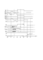
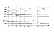
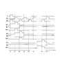
- FIGS. 4A and 4B are time charts showing an operation example of the shift register 121 in the first embodiment
- FIG. 4A is a time chart during normal operation
- FIG. 4B is a time chart during all-on operation.
- the high level and low level of the gate start pulse signal GST and the gate clock signals GCK1 and GCK2 are signal levels corresponding to the operating voltage VDD and the ground voltage VSS supplied to the shift register, respectively. is there.
- the gate all-on control signal GAON is set to a low level. Further, in FIGS.
- N11, N21 represents node N1, N2 of the first-stage shift register unit circuits 121 1, N12, N22 are the second-stage shift register unit circuits 121 2 nodes N1, N2 N1n and N2n represent nodes N1 and N2 of the n-th shift register unit circuit 121n, and OUT1, OUT2 and OUTn represent output signals of the first-stage, second-stage and n-th shift register unit circuits, respectively.
- the gate all-on control signal GAON is set to a low level.
- the thin film transistors T7 and T3B are maintained in the off state.
- the gate start pulse signal GST input to the first stage of the shift register unit circuit 121 1 of the set terminal SET is changed to a high level, is inputted to a clock terminal CKB
- the gate clock signal GCK2 transitions to a high level
- the thin film transistor T3A is turned on.
- the gate clock signal GCK2 input to the clock terminal CKB changes to a high level
- the gate start pulse signal GST input to the set terminal SET also changes to a high level.
- the thin film transistors T1 and T2 Turn on together. At this time, since the current supplied from the thin film transistor T1 is suppressed by the resistor R1, the signal level of the node N21 becomes a low level near the ground voltage VSS by the thin film transistor T2. When the node N21 becomes low level, both the thin film transistors T4 and T6 are turned off. As a result, the node N11 is charged by the thin film transistor T3A to a voltage (VDD ⁇ Vth) that is lowered by the threshold voltage Vth from the power supply voltage VDD (the high level of the gate clock signal GCK2 input to the clock terminal CKB).
- the gate clock signal GCK1 input to the clock terminal CK transits to a high level at time t1
- the high level of the gate clock signal GCK1 is changed to the output terminal OUT through the thin film transistor T5 having a drain connected to the clock terminal CK.
- the signal level of the output signal OUT1 starts to rise.
- the signal level of the output signal OUT1 rises, the signal level of the node N11 is pushed up by the bootstrap effect due to the capacitive component between the gate and source of the thin film transistor T5.
- the gate voltage of the thin film transistor T5 becomes higher than the source voltage of the thin film transistor T5, and the thin film transistor T5 is turned on.
- the high level of the gate clock signal GCK1 input to the clock terminal CK (the signal level corresponding to the power supply voltage VDD) is transmitted to the output terminal OUT without causing a voltage drop due to the threshold voltage Vth of the thin film transistor T5. .
- the thin film transistor T1 is turned on, the node N21 is charged through the thin film transistor T1 and the resistor R1, and the voltage of the node N21 is changed.
- the thin film transistors T4 and T6 whose gates are connected to the node N21 are turned on, and the thin film transistors T4 and T6 pull down the node N11 and the output terminal OUT, respectively.
- the thin film transistor T5 whose gate is connected to the node N11 is turned off, and the output signal OUT1 transitions to a low level.
- the thin film transistor T2 is maintained in the off state. Further, the thin film transistor T1 is periodically turned on in response to the high level of the gate clock signal GCK2 periodically input to the clock terminal CKB, so that the node N21 is maintained in the charged state. As a result, the thin film transistors T4 and T6 whose gates are connected to the node N21 are maintained in the on state. In this case, every time a high level pulse of the gate clock signal GCK2 arrives, the thin film transistor T3A is periodically turned on, and the gate start pulse signal GST at the low level is transmitted to the node N11 through the thin film transistor T3A. .
- the node N11 is periodically discharged through the thin film transistor T3A.
- the signal level of the node N11 is maintained at a low level corresponding to the ground potential VSS.
- the thin film transistor T5 whose gate is connected to the node N11 is maintained in the off state, and the output signal OUT1 is maintained at the low level by the thin film transistor T6 maintained in the on state.
- 2-stage shift register unit circuits 121 2 operation receives the output signal OUT1 of the first stage of the shift register unit circuits 121 1, only one clock half delay with respect to the first stage of the shift register unit circuit 121 1 of operation Implemented.
- the operation itself is the same as the shift register unit circuit 121 1 of the first stage, the shift register unit circuits 121 2 are output only at a later time t2 1 clock half than the output signal OUT1 of the first stage of the shift register unit circuits 121 1
- the signal OUT2 is changed to a high level.
- the shift register unit circuits 121 3 ,..., 121 n in the third and subsequent stages are delayed by a half clock with respect to the output signal of the previous shift register unit circuit, respectively, and the output signals OUT3, ..., OUTn are sequentially output.
- the all-on operation of the shift register 121 will be described with reference to FIG. 4B.
- the thin film transistor T3A is turned off, and the node N1 is pulled down by the thin film transistor T3B.
- the gate all-on control signal GAON is set to a high level.
- the gate start pulse signal GST is set to a high level
- the gate clock signals GCK1 and GCK2 are set to a low level.
- a thin film transistor T1 whose gate is connected to the clock terminal CKB of the gate clock signal GCK2 which is set to the low level is inputted is turned off. Further, the thin film transistor T2 whose gate is connected to the set terminal SET to which the gate start pulse signal GST set to the high level is input is turned on. As a result, the node N21 is pulled down by the thin film transistor T2, and the signal level of the node N21 becomes a low level. As a result, both the thin film transistors T4 and T6 whose gates are connected to the node N21 are turned off.
- the thin film transistor T3A whose gate is connected to the clock terminal CKB to which the gate clock signal GCK2 set to the low level is input is turned off.
- the thin film transistor T3B whose gate is connected to the all-on control terminal AON to which the high-level gate all-on control signal GAON is applied is turned on, and the node N11 is pulled down.
- the thin film transistor T5 is controlled to be in an off state in the all-on operation.
- the thin film transistor T7 whose gate is connected to the all-on control terminal AON to which the gate all-on control signal GAON set to the high level is applied is turned on.
- the power supply voltage VDD is supplied to the output terminal OUT through the thin film transistor T7, and the signal level of the output terminal OUT is set to a high level by the thin film transistor T7.
- the signal level of the output terminal OUT is increased by the thin film transistor T7 without being affected by the thin film transistors T5 and T6. Set to level.
- the shift register unit circuit 121 1 of the first stage outputs an output signal OUT1 of high level.
- a plurality of shift register unit circuits 121 1, 121 2, 121 3, ..., 121 of n the shift register unit circuit of odd number stage of the shift register unit circuits 121 1 similarly to the gate clock signal GCK1, GCK2 is input operates similarly to the shift register unit circuit 121 1 of the first stage in the all-on operation, and outputs an output signal of high level.
- the gate clock signals GCK1 and GCK2 input to the clock terminals CK and CKB are opposite to those in the odd-numbered shift register unit circuit.
- the signal levels of the clock signals GCK1 and GCK2 are both set to a low level.
- the signal level input to each terminal of the even-numbered shift register unit circuit is the same as the signal level input to each terminal of the odd-numbered shift register unit circuit. Accordingly, the all-on operation of the even-numbered shift register unit circuit is also explained in the same manner as the odd-stage shift register unit circuit, and the even-numbered shift register unit circuit outputs a high-level output signal in the all-on operation. As described above, the shift register 121 outputs the high level output signals OUT1, OUT2,..., OUTn as the gate signals G1, G2,. The all-on operation of the shift register 131 included in the signal line driver circuit 130 is also described in the same manner as the shift register 121 included in the scan line driver circuit 120 described above.
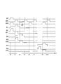
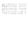
- FIG. 5 is a time chart for explaining the operation in the on sequence of the display device 100 according to the first embodiment.
- the potential of the video signal line (signal line of the data signal VIG), the potential of the counter electrode Tcom, or the potential of the auxiliary capacitance electrode line CSL becomes unstable, so that unintended charges are accumulated in the pixel portion PIX.
- Such a phenomenon is caused by the fact that the logic control of the circuit in the apparatus is not normally performed when the power supply circuit 150 is not reliably started up. Specifically, this phenomenon is caused by unnecessary charges entering the pixel portion PIX from the signal line of the data signal VSIG, and the potential of the counter electrode Tcom and the potential of the auxiliary capacitance electrode line CSL become unstable. This is because a potential difference is generated between Tcom and a pixel electrode (not shown), and unnecessary charges are accumulated in the pixel portion PIX due to the potential difference. This phenomenon causes image noise.
- the pixel thin film transistor TC of the pixel portion PIX is made conductive when the power is turned on so that charges are instantaneously discharged from all the pixel portions PIX. If charges are instantaneously released from the pixel portion PIX, it is not perceived as a change in the image by human vision, so that the viewer is hardly discomforted.
- the gate all-on control signal GAON and the source all-on control signal SAON are set to the active state (high level) and all Turn on the operation.
- the pixel thin film transistors TC of all the pixel portions PIX are turned on, and an initial voltage representing, for example, black is written in the pixel portions PIX as the data signal VSIG.
- the gate full-on control signal GAON and the source full-on control signal SAON are maintained in an active state, and the positive power supply voltage VH (positive high voltage) and negative power supply voltage VL (negative high voltage) generated in the power supply circuit 150 are maintained.
- the gate all-on control signal GAON and the source all-on control signal SAON are deactivated (low level), and the all-on operation is stopped. Thereafter, the gate start pulse signal GST and the gate clock signals GCK1 and GCK2 are generated at time t5, and the normal operation is started at time t6.
- the all-on operation is performed in a period in which the power supply voltage is unstable immediately after the power is turned on.
- the initial voltage representing black is written in all the pixel portions PIX, and black is displayed on the entire screen. . Thereby, the disturbance of the image when the power is turned on is suppressed, and the uncomfortable feeling given to the viewer can be alleviated.
- the initial voltage of the data signal VSIG is not limited to black, and a voltage representing any gradation can be set.
- FIG. 6A shows the operation when the scanning line is controlled to a high level in the all-on operation.
- FIG. 6B shows the operation when both the scanning line and the signal line are controlled to the high level in the all-on operation.
- the gate all-on control signal GAON is set to the active state
- the source all-on control signal SAON is set to the inactive state.
- the shift register 121 of the scanning line driving circuit 120 performs the all-on operation described above, and the gate signals G1, G2,..., Gn supplied from the shift register 121 to the scanning lines GL1, GL2,. All become high level.
- the pixel thin film transistors TC of all the pixel portions PIX are turned on at the same time.
- each of the plurality of pixel portions PIX connected to the same signal line SL is in a state where positive charges or negative charges are accumulated according to the content of the display image. That is, among the plurality of pixel portions PIX connected to the same signal line SL, positive charges are accumulated in some of the pixel portions PIX, and negative charges are accumulated in some of the other pixel portions PIX. It is in the state. Therefore, if all the signal line selection thin film transistors TS1, TS2,..., TSm shown in FIG.
- both the gate all-on control signal GAON and the source all-on control signal SAON are activated.
- both the gate full-on control signal GAON and the source full-on control signal SAON are both activated, and the output signals of the shift register 131 of the signal line driver circuit 130 are simultaneously high.
- the output signals of the shift registers 121 of the scanning line driving circuit 120 are simultaneously set to the high level.
- the display device 100 performs any AC driving such as dot inversion driving, scanning signal line inversion driving, and data signal line inversion driving, from time t3 to time t5.
- any AC driving such as dot inversion driving, scanning signal line inversion driving, and data signal line inversion driving
- each pixel unit PIX is discharged or charged so that the charge states of all the pixel units PIX are in a predetermined state. For this reason, compared with the example shown in FIG. 6A described above, it is possible to more stably suppress image disturbance when the power is shut off.
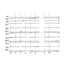
- FIG. 7 is a time chart for explaining the operation at the time of forced shut-off of the display device 100 according to the first embodiment.
- the scanning line driving circuit 120 performs normal operation.
- both the gate all-on control signal GAON and the source all-on control signal SAON are in an inactive state (that is, low level).
- the display control circuit 140 simultaneously turns off the gate all at the same time as the operation of the power supply circuit 150 is stopped.
- the control signal GAON and the source full-on control signal SAON are set to the active state (that is, high level).
- the capacitors C120, C130, etc. are formed in the output wiring of the power supply circuit 150, the gate full-on control signal GAON and the source output from the display control circuit 140 even when the power supply circuit 150 stops operating.
- the signal level of the all-on control signal SAON does not instantaneously become the ground voltage VSS, but gradually decreases toward the ground voltage VSS according to the time constant due to the capacity of the output wiring of the power supply circuit 150. In this case, since the signal levels of the other control signals are similarly lowered, the gate full-on control signal GAON and the source full-on control signal SAON are maintained relatively active, and the full-on operation is continued after time t4.
- the shift register 121 of the scanning line driving circuit 120 performs the all-on operation, and the scanning lines GL1, , GLn output high level output signals OUT1, OUT2,..., OUTn.
- the shift register 131 of the signal line driver circuit 130 is also turned on and outputs a high level output signal to the signal lines SL1, SL2,.
- VH does not instantaneously reach a level corresponding to the ground voltage VSS, but gradually decreases toward the ground voltage VSS according to the time constant of the capacitors C120 and C130.
- the positive power supply voltage VH of the power supply circuit 150 starts to decrease at time t4 and decreases to a low level corresponding to the ground potential VSS at time t5.
- the negative power supply voltage VL output from the power supply circuit 150 does not instantaneously reach a level corresponding to the ground voltage VSS, but gradually increases toward the ground voltage VSS according to the time constant of the capacitors C120 and C130.
- the gate signals G1, G2, G3,..., Gn on the scanning lines GL1, GL2,..., GLn gradually decrease from time t4 as the positive power supply voltage VH output from the power supply circuit 150 decreases. At t5, the level becomes low corresponding to the ground voltage VSS.
- the shift register 121 performs the all-on operation, so that all the signal levels of the scanning lines GL1, GL2,. And then gradually decreases with a constant time constant. That is, the signal levels of all the scanning lines GL1, GL2,.
- the NMOS transistors Q6 and Q8 that are specifically provided for the above-described prior art current blocking, and the node N1 is charged by one thin film transistor T3A.
- the number of transistors in each shift register included in the line driver circuit 120 and the signal line driver circuit 130 can be reduced, and the device configuration can be simplified. Accordingly, the layout area of the shift register that forms the scan line driver circuit 120 and the signal line driver circuit 130 can be reduced, and the display device 100 having the all-on operation function can be narrowed.
- the gate all-on control signal GAON is not used as the control signal for controlling the all-on operation without using the gate all-on control signal GAONB which is an inverted signal of the gate all-on control signal GAON. Therefore, it is possible to reduce the number of terminals, the number of signals, and the number of wires for controlling the all-on operation, and further narrow the frame.
- the thin film transistor T1 (FIG. 3) is turned off during the all-on operation, the through current path formed by the thin film transistor T1, the resistor R1, and the thin film transistor T2 is blocked.
- the thin film transistor T4 is turned off during the all-on operation, the through current path formed by the thin film transistors T3A and T4 is interrupted.
- the thin film transistors T5 and T6 are both turned off during the all-on operation, the through current path formed by the thin film transistors T5 and T6 is also blocked. Therefore, according to the present embodiment, it is possible to prevent a through current in the shift register during the all-on operation.
- the input signal of the set terminal SET set to the high level is supplied to the gate of the thin film transistor T5 through one thin film transistor T3A, so that the gate voltage of the thin film transistor T5 is reduced. Can be kept to a minimum. That is, since the node N1 is charged by one thin film transistor T3A, the voltage drop due to the threshold voltage Vth of the transistor can be minimized, and the operation margin can be improved. Therefore, the shift operation of the shift register can be stabilized during normal operation.
- the signal level when the gate all-on control signal GAON and the source all-on control signal SAON are active is set to the high level, but all signals are set to the low level (the ground voltage VSS) at the time of a power failure. If the signal level of the gate all-on control signal GAON and the source all-on control signal SAON becomes active, the signal level may be set to the low level. In this case, the gate full-on control signal GAON and the source full-on control signal SAON are set to a high level during normal operation, and the gate full-on control signal GAON and the source full-on control signal are forcibly cut off. Since the SAON signal level is set to a low level, it is possible to stably maintain the all-on operation after the forced cutoff.
- FIG. 1 and FIG. 2 used in the first embodiment are used.
- the shift register unit circuits 121 1 , 121 2 , 121 3 ,..., 121 n constituting the shift register 121 shown in FIG. instead of the shift register unit circuit 1211), a shift register unit circuit 1212 shown in FIG. 8 is provided.
- Other configurations are the same as those of the first embodiment.
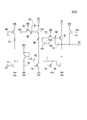
- FIG. 8 is a circuit diagram showing a configuration example of the shift register unit circuit 1212 in the second embodiment.
- the shift register unit circuit 1212 further includes a thin film transistor T8 in the configuration of the shift register unit circuit 1211 in the first embodiment shown in FIG.
- a current path is interposed between the clock terminal CKB and the gate of the thin film transistor T3A, and a power supply voltage VDD (predetermined potential) that applies a signal level for turning on the thin film transistor T8 is applied to the gate.
- VDD predetermined potential
- a connection point between the current path of the thin film transistor T8 and the gate of the thin film transistor T3A forms a node N3.
- Other configurations are the same as those of the shift register unit circuit 1211 in the first embodiment.
- each of the shift register unit circuits 121 1 , 121 2 , 121 3 ,..., 121 n in the first embodiment shown in FIG. 2 is replaced with a shift register unit circuit 1212 shown in FIG.
- the expression “shift register unit circuits 121 1 , 121 2 , 121 3 ,..., 121 n ” shown in FIG. Therefore, in this embodiment, each of “shift register unit circuits 121 1 , 121 2 , 121 3 ,..., 121 n ” indicates the shift register unit circuit 1212 shown in FIG. The same applies to each embodiment described later except for the eighth embodiment.
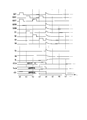
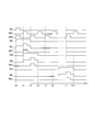
- FIGS. 9A and 9B are time charts showing an operation example of the shift register 1212 in the second embodiment
- FIG. 9A is a time chart during normal operation
- FIG. 9B is a time chart during all-on operation. Note that, in FIGS.
- N11, N31 represents node N1, N3 of the first-stage shift register unit circuits 121 1, N12, N32 is 2-stage shift register unit circuits 121 2 nodes N1, N3 N1n and N3n represent nodes N1 and N3 of the n-th shift register unit circuit 121n, and OUT1, OUT2 and OUTn represent output signals of the first-stage, second-stage and n-th shift register unit circuits, respectively.
- the normal operation of the shift register 1212 will be described with reference to FIG. 9A.
- the clock signal GCK2 input to the clock terminal CKB of the first-stage shift register unit circuit 121 1 that is, the first-stage shift register unit circuit 1212
- the signal level of the clock signal GCK2 is transmitted to the gate of the thin film transistor T3A through the thin film transistor T8.
- the node N31 between the gate of the thin film transistor T3A and the thin film transistor T8 is charged, and the voltage of the node N31 starts to rise.
- the thin film transistor T3A When the voltage at the node N31 rises, the thin film transistor T3A is turned on.
- the gate start pulse signal GST is given to the set terminal SET connected to the drain of the thin film transistor T3A as an input signal set to a high level, when the thin film transistor T3A is turned on, the source voltage is changed to the gate. The voltage drops from the voltage by the threshold voltage Vth. Therefore, the node N11 to which the source of the thin film transistor T3A is connected is charged following the node N31 to which the gate of the thin film transistor T3A is connected, and the voltage at the node N11 starts to rise.
- the thin film transistor T8 is turned off and the node N31 enters a floating state. Thereafter, in the process in which the node N11 is charged by the thin film transistor T3A and the voltage of the node N11 rises, through the capacitive component between the source and gate of the thin film transistor T3A, the capacitive component between the channel and gate of the thin film transistor T3A, etc. The voltage at the node N31 is pushed up by the voltage at the node N11.
- the voltage at the node N31 rises, and when the voltage exceeds the high level (power supply voltage VDD) of the gate start pulse signal GST plus the threshold voltage Vth of the thin film transistor T3A, a voltage drop due to the threshold voltage Vth of the thin film transistor T3A occurs. Instead, the node N11 is charged to the power supply voltage VDD by the thin film transistor T3A.
- the thin film transistor T8 having one end of the current path connected to the clock terminal CKB is turned on. For this reason, the node N31 is discharged by the thin film transistor T8, and the signal level of the node N31 becomes a low level.
- the thin film transistor T3A whose gate is connected to the node N31 is turned off. At this time, the node N11 is in a floating state and is maintained charged to the power supply voltage VDD, so that the thin film transistor T5 whose gate is connected to the node N11 is maintained in the on state.
- the gate clock signal GCK1 input to the clock terminal CK transitions to a high level at time t1
- the signal level (high level) of the gate clock signal GCK1 is transmitted to the output terminal OUT through the thin film transistor T5 and output.
- a high level is output as the signal OUT1.
- Other operations are the same as those of the shift register 1211 in the first embodiment.
- the all-on operation is the same as that in the first embodiment as shown in FIG. 9B. That is, in the all-on operation, the gate all-on control signal GAON is set to a high level. As shown in FIG. 9B, the gate start pulse signal GST is set to a high level, and the gate clock signals GCK1 and GCK2 are set to a low level. In this case, in the first stage of the shift register unit circuits 121 1, a thin film transistor T1 is turned off, the thin-film transistor T2 is turned on. As a result, the node N21 is pulled down by the thin film transistor T2, and the signal level becomes low. As a result, both the thin film transistors T4 and T6 whose gates are connected to the node N21 are turned off.
- the thin film transistor T3A since the clock terminal CKB to which the gate clock signal GCK2 set to the low level is input is given to the gate of the thin film transistor T3A through the thin film transistor T8, the thin film transistor T3A is turned off. For this reason, the gate start pulse signal GST input to the set terminal SET as an input signal set to the high level is not transmitted to the node N11. In this case, the thin film transistor T3B connected between the node N11 and the ground node is turned on. As a result, the node N11 becomes low level, and the thin film transistor T5 whose gate is connected to the node N11 is turned off.
- the thin film transistor T7 whose gate is connected to the all-on control terminal AON to which the gate all-on control signal GAON set to the high level is applied is turned on.
- the power supply voltage VDD is supplied to the output terminal through the thin film transistor T7, thereby setting the output terminal OUT to the high level.
- the output terminal OUT is set to a high level by the thin film transistor T7 without being affected by the thin film transistors T5 and T6.
- the shift register unit circuit 121 1 of the first stage outputs an output signal OUT1 of high level.
- the second and subsequent stages shift register unit circuit 121 2, 121 3, ..., the output signal OUT2 of 121 n, OUT3, ..., OUTn also set in the same manner as the output signal OUT1 of the first stage of the shift register unit circuits 121 1 to the high level Is done.
- the scanning line driving circuit 120 including the shift register unit circuit 1212 according to the present embodiment outputs the high-level output signals OUT1, OUT2,..., OUTn as the gate signals G1, G2,. All-on operation is performed.
- the gate voltage of the thin film transistor T3A is higher than that of the first embodiment. Therefore, waveform distortion of the signal transmitted through the thin film transistor T3A can be suppressed. Therefore, for example, even if the threshold voltage Vth of the thin film transistor increases due to the influence of the initial characteristics, temperature characteristics, deterioration, etc., the deterioration of the signal in the shift register can be suppressed, and the operation margin of the shift register is improved. be able to.
- FIG. 1 and FIG. 2 used in the first embodiment are used.
- the shift register unit circuit 1211 shown in FIG. 10 is provided instead of the shift register unit circuit 1211) shown in FIG.
- Other configurations are the same as those of the second embodiment.
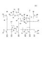
- FIG. 10 is a circuit diagram showing a configuration example of the shift register unit circuit 1213 in the third embodiment.
- the shift register unit circuit 1213 further includes capacitors C1, C2, and C3 in the configuration of the shift register unit circuit 1212 in the second embodiment shown in FIG.
- the capacitor C1 is connected between the drain and gate of the thin film transistor T5.
- the capacitor C3 is connected between the drain and gate of the thin film transistor T3A.
- the capacitor C2 is connected between a node N2 to which the gates of the thin film transistors T4 and T6 are connected and a ground node (predetermined potential node).
- Other configurations are the same as those of the shift register unit circuit 1212 in the second embodiment. Note that it is not necessary to provide all of the capacitors C1, C2, and C3, and any one or two of them may be provided.
- the basic operation is the same as that of the shift register unit circuit 1212 in the second embodiment, but in this embodiment, the self-bootstrap effect of the thin film transistor T5 in the normal operation can be enhanced by the capacitor C1.
- the gate voltage of the thin film transistor T5 when the thin film transistor T5 is turned on can be effectively increased. Therefore, the signal level can be transmitted to the output terminal OUT without deteriorating the signal level transmitted from the clock terminal CK to the output terminal OUT through the thin film transistor T5.
- the capacitor C3 can enhance the bootstrap effect of the thin film transistor T3A. Accordingly, it is possible to effectively increase the gate voltage of the thin film transistor T3A when the input signal applied to the set terminal SET transitions to a high level and the thin film transistor T3A is turned on. Accordingly, the signal level can be transmitted from the set terminal SET to the node N1 through the thin film transistor T3A without deteriorating the signal level. Further, the capacitor C2 can increase the voltage holding capability of the node N2. Accordingly, the thin film transistors T4 and T6 can be stably maintained in the off state while the node N1 is charged, and the shift operation can be stabilized.
- the increase in the voltage of the node N1 or the node N3 due to the bootstrap effect can be improved, so that the thin film transistors T3A and T5 are stably controlled to be in the on state. can do. Therefore, the operation margin of the shift register can be improved.
- the all-on operation is the same as in the first and second embodiments described above.
- FIG. 1 and FIG. 2 used in the first embodiment are used.
- the shift register unit circuit 1214 shown in FIG. 11 is provided instead of the shift register unit circuit 1211 shown in FIG.
- Other configurations are the same as those of the third embodiment.
- FIG. 11 is a circuit diagram showing a configuration example of the shift register unit circuit 1214 in the fourth embodiment.
- the shift register unit circuit 1214 further includes a thin film transistor T9 in the configuration of the shift register unit circuit 1213 in the third embodiment shown in FIG.
- the thin film transistor T9 has a gate connected to the drain of the thin film transistor T6, a drain connected to the gate of the thin film transistor T6, and a source connected to the ground node (predetermined potential node). That is, the thin film transistor T6 and the thin film transistor T9 have a gate and a drain that are cross-coupled.
- Other configurations are the same as those of the shift register unit circuit 1213 in the third embodiment.
- the basic operation is the same as that of the shift register unit circuit 1212 in the third embodiment described above, but in this embodiment, the output terminal in the period from time t1 to time t2 shown in FIG. 9A in the second embodiment described above.
- the high level of the output signal of OUT can be stably maintained. This will be described with reference to the time chart of FIG. 9A.
- the thin film transistors T1 and T2 are turned on. Among these, the thin film transistor T2 causes the node N2 to be at a low level. Driven by.
- the gate start pulse signal GST and the gate clock signal GCK2 transition to a low level
- the thin film transistors T1 and T2 are turned off, and the node N2 is in a floating state.
- the signal level (that is, the low level) up to that point of the node N2 is held by the capacitance (eg, the capacitance of the capacitor C2) formed at the node N2.
- the gate clock signal GCK1 transitions to the high level at time t1, as described above, the high level is output to the output terminal OUT through the thin film transistor T5.
- the thin film transistor T6 needs to be maintained in the off state during a period in which a high level is output to the output terminal OUT through the thin film transistor T5 from the time t1.
- the node N2 to which the gate of the thin film transistor T6 is connected is maintained in a floating state during the period when the output signal of the output terminal OUT is at the high level at time t1.
- the signal level of the gate of the thin film transistor T6 is maintained at a low level by the capacitance formed at the node N2, and the signal level is unstable. Therefore, for example, when the signal level of the node N2 rises due to the presence of noise or a leakage path, the thin film transistor T6 may be turned on to lower the signal level (high level) of the output terminal OUT.
- the fourth embodiment when the signal level of the output terminal OUT becomes high due to the presence of the above-described noise and leak path, the signal level of the gate of the thin film transistor T9 becomes high. For this reason, the thin film transistor T9 is turned on, and the node N2 to which the gate of the thin film transistor T6 is connected is driven to a low level (ground voltage VSS). Thus, the thin film transistor T6 is forcibly maintained in the off state by the thin film transistor T9 during a period in which the signal level of the output terminal OUT is high from time t1. Therefore, according to the present embodiment, in normal operation, the output signal can be stably maintained at a high level, and malfunction due to a decrease in the signal level of the output signal can be prevented. Therefore, the operation margin of the shift register can be improved.
- the all-on operation is the same as in the first to third embodiments described above.
- FIG. 1 and FIG. 2 used in the first embodiment are used.
- shift register unit circuits 121 1 , 121 2 , 121 3 ,..., 121 n constituting the shift register 121 shown in FIG. 12 is provided instead of the shift register unit circuit 1211) shown in FIG.
- Other configurations are the same as those of the fourth embodiment.
- FIG. 12 is a circuit diagram showing a configuration example of the shift register unit circuit 1215 in the fifth embodiment.
- the shift register unit circuit 1215 further includes a thin film transistor T10 in the configuration of the shift register unit circuit 1214 in the fourth embodiment shown in FIG.
- the source of the thin film transistor T10 is connected to the node N2 to which the gates of the thin film transistors T6 and T4 are connected, and the initialization signal INIT is applied to the gate and drain of the thin film transistor T10. That is, the thin film transistor T10 is diode-connected, the initialization signal INIT is given to the node corresponding to the anode, and the node corresponding to the cathode is connected to the node N2 to which the gates of the thin film transistors T4 and T6 are connected.
- the Other configurations are the same as those of the shift register unit circuit 1214 in the fourth embodiment.
- the initialization signal INIT is a signal that is set to an active state (high level) by, for example, the display control circuit 140 when the power is turned on, when the power is turned off, or when the shift register is temporarily set to an initial state. However, in the all-on operation, the initialization signal INIT is set to an inactive state (low level).
- the initialization signal INIT is activated, the drain and gate voltages of the thin film transistor T10 rise, and a voltage is generated at the source of the thin film transistor T10 by dropping the drain voltage by the threshold voltage Vth.
- the high level of the initialization signal INIT is the power supply voltage VDD
- a voltage (VDD ⁇ Vth) obtained by subtracting the threshold voltage Vth of the thin film transistor T10 from the power supply voltage VDD is generated at the source of the thin film transistor T10.
- the source voltage (VDD ⁇ Vth) of the thin film transistor T10 is applied to the node N2
- the thin film transistors T4 and T6 are forcibly turned on. Therefore, the node N1 is discharged by the thin film transistor T4, and the output terminal OUT is pulled down by the thin film transistor T6.
- the circuit state of the shift register unit circuit 1215 is initialized and the signal level of the output signal is initialized to a low level.
- the circuit state of the shift register is structurally initialized regardless of the signals input to the clock terminals CK, CKB, the set terminal SET, and the like.
- the shift register can be stably controlled to be inactive and the output signal can be set to a low level.
- the thin film transistor T10 is diode-connected, but the drain of the thin film transistor T10 may be fixed to the power supply voltage VDD and the initialization signal INIT may be input to the gate.
- the all-on operation is the same as in the first to fourth embodiments described above.
- FIG. 1 and FIG. 2 used in the first embodiment are used.
- the display device according to the sixth embodiment has shift register unit circuits 121 1 , 121 2 , 121 3 ,..., 121 n (that is, FIG. 3) that constitute the shift register 121 shown in FIG.
- the shift register unit circuit 1211) shown in FIG. 13 is provided instead of the shift register unit circuit 1211) shown in FIG.
- Other configurations are the same as those of the fifth embodiment.
- FIG. 13 is a circuit diagram showing a configuration example of the shift register unit circuit 1216 in the sixth embodiment.
- the shift register unit circuit 1216 further includes a thin film transistor T11 in the configuration of the shift register unit circuit 1215 in the fifth embodiment shown in FIG.
- the thin film transistor T11 has a current path interposed between the drain of the thin film transistor T3A and the gate of the thin film transistor T5. Specifically, one of the source and drain forming the current path of the thin film transistor T11 is connected to the source of the thin film transistor T3A, and the other of the source and drain of the thin film transistor T11 is connected to the gate of the thin film transistor T5.
- a power supply voltage VDD predetermined potential
- connection point between the source of the thin film transistor T3A and the drain of the thin film transistor T4 forms a node N4
- connection point between the current path of the thin film transistor T11 and the gate of the thin film transistor T5 forms a node N5.
- Other configurations are the same as those of the shift register unit circuit 1215 in the fifth embodiment.
- the shift register unit circuit 1215 in the fifth embodiment described above when the voltage of the node N1 is pushed up by the bootstrap effect by the capacitor C1, the voltage becomes a high voltage (VDD + ⁇ ) higher than the power supply voltage VDD. At this time, a difference voltage between the high voltage (VDD + ⁇ ) and the ground voltage VSS is applied between the gate and the drain of the thin film transistor T3A and between the source and the drain in combination with the bootstrap effect by the capacitor C3. And a very high voltage is applied. The same applies to the thin film transistor T4. The differential voltage between the high voltage (VDD + ⁇ ) and the ground voltage VSS is also applied between the gate and drain of the thin film transistor T4 and between the source and drain. Such a high voltage can cause deterioration of the transistor, for example. In the sixth embodiment, as described below, in the operation of the shift register unit circuit 1216, the above-described high voltage generation in the fifth embodiment is prevented by the thin film transistor T11.
- FIGS. 14A and 14B are time charts showing an operation example of the shift register 121 including the shift register unit circuit 1216 in the sixth embodiment
- FIG. 14A is a time chart at the time of normal operation
- FIG. It is a time chart at the time of operation.
- the high level and low level of the gate start pulse signal GST and the gate clock signals GCK1 and GCK2 are signal levels corresponding to the operating voltage VDD and the ground voltage VSS supplied to the shift register, respectively. is there.
- the gate all-on control signal GAON is set to a low level. Further, in FIGS.
- N41, N51 represents the first stage of the shift register unit circuit 121 1 of the node N4, N5, N42, N52 are the second-stage shift register unit circuits 121 2 nodes N4, N5 N4n and N5n represent nodes N4 and N5 of the n-th shift register unit circuit 121n, and OUT1, OUT2 and OUTn represent the first, second and n-th shift register unit circuits, respectively. It represents the output signal.
- “H” indicates a high level
- “L” indicates a low level.
- the basic operation of the shift register unit circuit 1216 is the same as the normal operation of each shift register unit circuit 1216 of the first to fifth embodiments described above, but in the sixth embodiment, the node N4 is charged, The behavior of the internal signal when outputting a high level as an output signal is different from that of the above-described embodiments.
- the gate clock signal GCK2 input to the clock terminal CKB of the first-stage shift register unit circuit 121 1 transitions to a high level at time t0.
- the signal level of the gate clock signal GCK2 is transmitted to the gate of the thin film transistor T3A through the thin film transistor T8.
- the node N31 between the gate of the thin film transistor T3A and the thin film transistor T8 is charged, and the voltage of the node N31 starts to rise.
- the thin film transistor T3A When the voltage at the node N31 rises, the thin film transistor T3A is turned on.
- the gate start pulse signal GST set to the high level is given to the set terminal SET to which the drain of the thin film transistor T3A is connected, when the thin film transistor T3A is turned on, the source voltage is changed from the gate voltage. The voltage drops by the threshold voltage Vth. Therefore, the node N41 to which the source of the thin film transistor T3A is connected is charged following the node N31 to which the gate of the thin film transistor T3A is connected, and the voltage at the node N41 starts to rise.
- the thin film transistor T8 is turned off and the node N31 enters a floating state. Thereafter, in the process in which the node N41 is charged by the thin film transistor T3A and the voltage at the node N41 increases, the voltage at the node N31 is pushed up by the voltage at the node N41 through the coupling capacitance (parasitic capacitance) between the source and gate of the thin film transistor T3A.
- the node N41 causes the power supply voltage VDD by the thin film transistor T3A without causing a voltage drop due to the threshold voltage Vth of the thin film transistor T3A. It is charged until.
- the power supply voltage VDD is applied to the gate of the thin film transistor T11 and the thin film transistor T11 is in the on state, when the node N41 is charged, the node N51 is also charged through the thin film transistor T11, and the signal level of the node N51 Rises. For this reason, the thin film transistor T5 whose gate is connected to the node N51 is turned on.
- the signal level of the gate clock signal CK1 input to the drain of the thin film transistor T5 connected to the clock terminal CK is low level, the signal level of the output signal of the output terminal OUT1 remains low level. is there.
- the node N5 is charged through the thin film transistor T11 to a voltage lower than the power supply voltage VDD by the threshold voltage Vth of the thin film transistor T11, the thin film transistor T11 is turned off, and the node N41 and the node N51 are electrically disconnected.
- the gate clock signal GCK1 input to the clock terminal CK transitions to a high level at time t1
- the signal level (high level) of the gate clock signal GCK1 is transmitted to the output terminal OUT through the thin film transistor T5 and output.
- a high level is output as the signal OUT1.
- the voltage of the node N51 is pushed up by the voltage of the output signal of the output terminal OUT to become a high voltage. Accordingly, the high level (power supply voltage VDD) of the gate clock signal GCK1 input to the clock terminal CK is transmitted to the output terminal OUT without causing a voltage drop due to the threshold voltage Vth of the thin film transistor T5.
- the thin film transistor T11 is turned off, so that the voltage at the node N41 is not pushed up by the bootstrap effect by the capacitor C1. Is maintained at the power supply voltage VDD. Therefore, according to the present embodiment, only the difference voltage between the power supply voltage VDD and the ground voltage VSS is applied to the thin film transistors T3A and T4, and no high voltage is applied.
- the voltage at the node N51 remains at a voltage (VDD ⁇ Vth + ⁇ ) obtained by adding a voltage ⁇ corresponding to the boosted voltage by the capacitor C1 to the voltage obtained by subtracting the threshold voltage Vth of the thin film transistor T11 from the voltage at the node N41. Therefore, only the difference voltage ( ⁇ Vth) between the voltage at the node N51 (VDD ⁇ Vth + ⁇ ) and the voltage at the node N41 (VDD) is applied to the thin film transistor T11.
- the voltage ⁇ corresponding to the increase due to the bootstrap effect by the capacitor C1 does not become larger than the amplitude (VDD ⁇ VSS) of the gate clock signal GCK1 input to the clock terminal CK. Only a voltage lower than the drive voltage is applied.
- Other normal operations are the same as those in the above-described embodiments.
- the all-on operation is the same as that in each of the above-described embodiments as shown in FIG. 14B. That is, in the all-on operation, the gate all-on control signal GAON is set to a high level. As shown in FIG. 14B, the gate start pulse signal GST is set to a high level, and the gate clock signals GCK1 and GCK2 are set to a low level. In this case, in the first stage of the shift register unit circuits 121 1, a thin film transistor T1 is turned off, the thin-film transistor T2 is turned on. As a result, the node N21 is pulled down by the thin film transistor T2, and the signal level becomes low. As a result, the thin film transistors T4 and T6 whose gates are connected to the node N21 are turned off.
- the thin film transistor T3A whose gate is connected to the clock terminal CKB to which the gate clock signal GCK2 set to the low level is input is turned off.
- the thin film transistor T3B whose gate is connected to the all-on control terminal AON to which the high-level gate all-on control signal GAON is applied is turned on, and the node N11 is pulled down.
- the thin film transistor T5 is controlled to be in an off state in the all-on operation.
- the thin film transistor T7 whose gate is connected to the all-on control terminal AON to which the gate all-on control signal GAON set to the high level is applied is turned on.
- the power supply voltage VDD is supplied to the output terminal OUT through the thin film transistor T7, and the output terminal OUT is set to the high level.
- the shift register unit circuit 121 1 of the first stage outputs an output signal OUT1 of high level.
- the second and subsequent stages shift register unit circuit 121 2, 121 3, ..., the output signal OUT2 of 121 n, OUT3, ..., OUTn also set in the same manner as the output signal OUT1 of the first stage of the shift register unit circuits 121 1 to the high level Is done.
- the shift register 121 including the shift register unit circuit 1216 outputs the high level output signals OUT1, OUT2,..., OUTn as the gate signals G1, G2,.
- the operation is performed.
- the voltage applied to each thin film transistor is relaxed, so that deterioration of the transistor and the like can be suppressed.
- FIG. 1 and FIG. 2 used in the first embodiment are used.
- shift register unit circuits 121 1 , 121 2 , 121 3 ,..., 121 n constituting the shift register 121 shown in FIG. instead of the shift register unit circuit 1211) shown in FIG. 15, a shift register unit circuit 1217 shown in FIG. 15 is provided.
- Other configurations are the same as those of the sixth embodiment.
- FIG. 15 is a circuit diagram showing a configuration example of the shift register unit circuit 1217 in the seventh embodiment.
- the shift register unit circuit 1217 further includes a thin film transistor T12 in the configuration of the shift register unit circuit 1216 in the sixth embodiment shown in FIG.
- the current path of the thin film transistor T12 is connected between the node N2 to which the gate of the thin film transistor T6 is connected and the ground node (predetermined potential node).
- the gate of the thin film transistor T12 is connected to the all-on control terminal AON, and the gate all-on control signal GAON is applied to the gate.
- Other configurations are the same as those of the shift register unit circuit 1216 in the sixth embodiment.
- the operation of the shift register unit circuit 1217 in this embodiment will be described.
- the normal operation is the same as that of the above-described sixth embodiment, so that the description thereof will be omitted and the all-on operation will be described.
- the gate all-on control signal GAON is set to a high level.
- the gate clock signals GCK1 and GCK2 are set to a low level.
- the gate start pulse signal GST may be high level or low level.
- the thin film transistor T2 When the gate start pulse signal GST input to the set terminal SET is at the high level, the thin film transistor T2 is turned on as in the above embodiments, and the node N2 is discharged by the thin film transistor T2. In this case, since the thin film transistor T12 whose gate is connected to the all-on control terminal AON is also turned on, the node N2 is discharged through the thin film transistor T12 together with the thin film transistor T2. As a result, the thin film transistors T4 and T6 whose gates are connected to the node N2 are both controlled to be turned off.
- the low level of the gate clock signal GCK2 input to the clock terminal CKB is given to the gate of the thin film transistor T3A through the thin film transistor T8. Thereby, the thin film transistor T3A is turned off.
- the high-level gate full-on control signal GAON is given to the full-on control terminal AON to which the gate of the thin-film transistor T3B is connected, the thin-film transistor T3B is turned on.
- the node N4 is discharged through the thin film transistor T3B.
- the discharged low level of the node N4 is transmitted to the gate of the thin film transistor T5 through the thin film transistor T11, thereby turning off the thin film transistor T5.
- both the thin film transistors T5 and T6 connected to the output terminal OUT are turned off.
- the thin film transistor T7 whose gate is connected to the all-on control terminal AON to which the gate all-on control signal GAON set to the high level is applied is turned on.
- the power supply voltage VDD is supplied to the output terminal OUT through the thin film transistor T7, and the output terminal OUT is set to the high level.
- the shift register unit circuit 121 1 of the first stage outputs an output signal OUT1 of high level.
- the second and subsequent stages shift register unit circuit 121 2, 121 3, ..., the output signal OUT2 of 121 n, OUT3, ..., OUTn also set in the same manner as the output signal OUT1 of the first stage of the shift register unit circuits 121 1 to the high level Is done. As a result, the all-on operation is performed when the gate start pulse signal GST is set to a high level.
- the shift register unit circuit 121 1 of the first stage outputs an output signal OUT1 of high level.
- the second and subsequent stages shift register unit circuit 121 2, 121 3, ..., the output signal OUT2 of 121 n, OUT3, ..., OUTn also set in the same manner as the output signal OUT1 of the first stage of the shift register unit circuits 121 1 to the high level Is done. As a result, the all-on operation is performed when the gate start pulse signal GST is set to a high level.
- the shift register 121 including the shift register unit circuit 1217 outputs the high level output signals OUT1, OUT2,..., OUTn as the gate signals G1, G2,. Is implemented. Therefore, according to the seventh embodiment, the shift register can be fully turned on regardless of the signal level of the gate start pulse signal GST input to the set terminal SET.
- FIG. 1 used in the first embodiment
- the display device according to the eighth embodiment includes a shift register 181 shown in FIG. 16 instead of the shift register 121 shown in FIG. 2 used in the seventh embodiment.
- Other configurations are the same as those of the first embodiment.
- FIG. 16 is a schematic block diagram illustrating a configuration example of the shift register 181 in the eighth embodiment.
- the shift register 181 includes a plurality of shift register unit circuits 181 1 , 181 2 , 181 3 ,..., 181 n corresponding to the plurality of scanning lines GL 1, GL 2, GL 3,. Yes.
- the plurality of shift register unit circuits 181 1 , 181 2 , 181 3 ,..., 181 n are connected in cascade.
- Each of the plurality of shift register unit circuits 181 1 , 181 2 , 181 3 ,..., 181 n has the same configuration, and hereinafter, the shift register unit circuits 181 1 , 181 2 , 181 3 , ..., when referring to each of the 181 n are referred to as "shift register unit circuits 1811".
- the shift register unit circuit 1811 includes clock terminals CK and CKB, two set terminals SET1 and SET2, an output terminal OUT, and an all-on control terminal AON.
- the gate clock signal GCK1 is input to the clock terminal CK of the odd-stage shift register unit circuit, and the gate clock is supplied to the clock terminal CKB.
- the signal GCK2 is input.
- the gate clock signal GCK2 is input to the clock terminal CK of the even-numbered shift register unit circuit, and the gate clock signal GCK1 is input to the clock terminal CKB.
- a plurality of shift register unit circuits 181 1, 181 2, 181 3, ..., the all-on control terminal AON of 181 n gate all-on control signal GAON is input.
- the gate start pulse signal GST is input to the set terminal SET 1 of the first-stage shift register unit circuit 181 1 .
- the output signal of the previous shift register unit circuit is input to each set terminal SET1 of the shift register unit circuit (that is, the second-stage shift register unit circuit to the n-th shift register unit circuit).
- the gate start pulse signal GST is input to the set terminal SET2 of the n-th shift register unit circuit 181n at the final stage, and the shift register unit circuit before the (n-1) th stage (that is, the first-stage shift register unit circuit).
- the output signal of the subsequent shift register unit circuit is input to the set terminal SET2.
- the shift register unit circuit 181 and second set terminal SET1 the output signal OUT1 of the preceding stage of the shift register unit circuits 181 1 are input to the shift register unit circuit 181 and second set terminal SET2, the subsequent shift register the output signal OUT3 of the unit circuit 181 3 is input.
- each of the plurality of shift register unit circuits 181 1 , 181 2 , 181 3 ,..., 181 n has a scanning switching signal UD described later for switching the scanning direction (shift direction). , UDB.
- FIG. 17 is a circuit diagram showing a configuration example of the shift register unit circuit 1811 in the eighth embodiment.
- the shift register unit circuit 1811 further includes a selection circuit SEL in the configuration of the shift register unit circuit 1217 in the seventh embodiment shown in FIG. Other configurations are the same as those of the shift register unit circuit 1217 of the seventh embodiment.
- the selection circuit SEL Based on the scan switching signals UD and UDB, the selection circuit SEL outputs the output signal (or gate start pulse signal GST) of the preceding shift register unit circuit input to the set terminal SET1 and the subsequent shift input to the set terminal SET2.
- One of the output signals (or gate start pulse signal GST) of the register unit circuit is selected and input as an input signal.
- the selection circuit SEL provided to the second-stage shift register unit circuit 181 2, the output signal OUT1 of the first stage of the shift register unit circuits 181 1, the output signal OUT3 of the shift register unit circuit 181 3 of the third stage One of the output signals is selected.
- the selection circuit SEL supplies the selected output signal to the gate of the thin film transistor T2, and also supplies it to the drain of the thin film transistor T3A connected to the set terminal SET in the seventh embodiment.
- the selection circuit SEL functions as a scanning switching circuit for switching the scanning direction based on the scanning switching signals UD and UDB.
- the scanning direction a plurality of shift register unit circuits 181 1, 181 2, 181 3 shown in FIG. 16, ..., the output signal of 181 n OUT1, OUT2, OUT3, ..., refers to output order of OUTn, the first stage .., OUTn is output in the ascending scanning direction from the shift register unit circuit 181 1 to the n-th shift register unit circuit 181 n as the final stage.
- the output signal from the shift register unit circuit 181 n is the final stage in the descending order of the scanning direction in the shift register unit circuit 181 1 of the first stage OUT1, OUT2, OUT3, ..., scanning when OUTn is output Is called reverse scanning.
- FIGS. 18A to 18C are circuit diagrams showing detailed examples of the shift register unit circuit in the eighth embodiment, and show a configuration example of the selection circuit SEL.
- the selection circuit (scan switching circuit) illustrated in FIG. 18A includes thin film transistors T81, T82, T83, T84, T85, T86, T87, and T88.
- a scanning switching signal UD is supplied to the drain of the thin film transistor T81
- a scanning switching signal UDB which is an inverted signal of the scanning switching signal UD is supplied to the gate thereof.
- the source of the thin film transistor T81 is connected to the drain of the thin film transistor T82, and the power supply voltage VDD is supplied to the gate of the thin film transistor T82.
- a scanning switching signal UD is supplied to the drain of the thin film transistor T83, its gate is connected to the drain, and its source is connected to the gate of the thin film transistor T84 together with the source of the thin film transistor T82. That is, the thin film transistor T83 is diode-connected, the scan switching signal UD is supplied to the node corresponding to the anode, and the node corresponding to the cathode is connected to the gate of the thin film transistor T84.
- One end of the current path of the thin film transistor T84 is connected to the set terminal SET1, and the other end of the current path is connected to the output terminal SO.
- the scanning switching signal UDB is supplied to the source of the thin film transistor T85, and the scanning switching signal UD is supplied to the gate thereof.
- the drain of the thin film transistor T85 is connected to the source of the thin film transistor T86, and the power supply voltage VDD is supplied to the gate of the thin film transistor T86.
- a scanning switching signal UDB is supplied to the source of the thin film transistor T87, its gate is connected to the source, and its drain is connected to the gate of the thin film transistor T88 together with the drain of the thin film transistor T86. That is, the thin film transistor T87 is diode-connected, the scan switching signal UDB is supplied to the node corresponding to the anode, and the node corresponding to the cathode is connected to the gate of the thin film transistor T88.
- One end of the current path of the thin film transistor T88 is connected to the set terminal SET2, and the other end of the current path is connected to the output terminal SO.
- the selection circuit shown in FIG. 18B omits the thin film transistors T81, T83, T85, and T87 in the configuration shown in FIG. 18A, supplies the scan switching signal UD to the drain of the thin film transistor T82, and supplies the scan switching signal UDB to the source of the thin film transistor T86. Configured to supply.
- the selection circuit shown in FIG. 18C omits the thin film transistors T81, T82, T83, T85, T86, and T87, supplies the scan switching signal UD to the gate of the thin film transistor T84, and supplies the gate of the thin film transistor T88.
- the scanning switching signal UDB is configured to be supplied.
- the scanning switching signal UD is set to a high level, and the scanning switching signal UDB, which is an inverted signal thereof, is set to a low level.
- the thin film transistor T81 to which the low level scan switching signal UDB is applied is turned off, and the gate of the thin film transistor T84 is set to the high level of the scan switching signal UD through the thin film transistor T83 to which the high level scan switching signal UD is applied to the drain.
- the corresponding power supply voltage VDD is charged to a voltage (VDD ⁇ Vth) dropped by the threshold voltage Vth of the thin film transistor T83. Accordingly, the thin film transistor T84 is turned on.
- the thin film transistor T85 to which the high-level scan switching signal UD is applied to the gate is turned on.
- the thin film transistor T86 to which the power supply voltage VDD is applied to the gate is also in the on state. Therefore, the gate of the thin film transistor T88 is discharged through the thin film transistors T85 and T86, and a low level is applied to the gate of the thin film transistor T88. Accordingly, the thin film transistor T88 is turned off. In this case, the thin film transistor T87 is turned off because the low-level scan switching signal UDB is supplied to the source and the gate.
- the set terminal SET1 is electrically connected to the output terminal SO, and the set terminal SET2 is electrically disconnected from the output terminal SO. Become. For this reason, a signal input to the set terminal SET1 is selected and output from the output terminal SO.
- the gate voltage of the thin film transistor T84 is pushed up by the signal level of the signal input to the set terminal SET1 due to the bootstrap effect due to the capacitive component between the gate and the channel of the thin film transistor T84. For this reason, the signal input to the set terminal SET1 is transmitted to the output terminal SO without causing a voltage drop due to the threshold voltage Vth of the thin film transistor T84.
- the output signal of the previous shift register unit circuit is input to the set terminal SET1, the plurality of shift register unit circuits 181 1 , 181 2 , 181 3 ,..., 181 n shown in FIG.
- the output signals OUT1, OUT2, OUT3,..., OUTn are output in ascending order, and forward scanning is performed.
- the scanning switching signal UD is set to a low level, and the scanning switching signal UDB is set to a high level.
- the thin film transistor T81 to which the high-level scan switching signal UDB is applied to the gate is turned on.
- the thin film transistor T82 to which the power supply voltage VDD is applied to the gate is also in the on state. Therefore, the gate of the thin film transistor T84 is discharged through the thin film transistors T81 and T82, and a low level is applied to the gate of the thin film transistor T84. Accordingly, the thin film transistor T84 is turned off. In this case, the thin film transistor T83 is turned off because the low-level scan switching signal UDB is supplied to the source and the gate.
- the thin film transistor T85 to which the low level scan switching signal UD is applied to the gate is turned off, and the gate of the thin film transistor T88 is connected to the high level of the scan switching signal UDB through the thin film transistor T87 to which the high level scan switching signal UDB is applied to the drain. Is charged to a voltage (VDD ⁇ Vth) dropped from the power supply voltage VDD corresponding to the threshold voltage Vth of the thin film transistor T87. Accordingly, the thin film transistor T88 is turned on.
- the set terminal SET2 is electrically connected to the output terminal SO, and the set terminal SET1 is electrically disconnected from the output terminal SO. Become. For this reason, the signal input to the set terminal SET2 is selected and output from the output terminal SO. At this time, the gate voltage of the thin film transistor T88 is pushed up by the signal level of the signal input to the set terminal SET2 due to the bootstrap effect due to the capacitive component between the gate and the channel of the thin film transistor T88. For this reason, the signal input to the set terminal SET2 is transmitted to the output terminal SO without causing a voltage drop due to the threshold voltage Vth of the thin film transistor T88.
- a signal is transmitted from the set terminal SET1 or the set terminal SET2 to the output terminal SO without causing a voltage drop due to the threshold voltage Vth of the thin film transistors T84 and T88. Can do. Therefore, it is possible to switch the scanning direction while securing the operation margin of the shift register unit circuit.
- the scanning switching signal UD is set to a high level, and the scanning switching signal UDB is set to a low level.
- the high-level scanning switching signal UD is transmitted to the gate of the thin film transistor T84 through the thin film transistor T82.
- the gate of the thin film transistor T84 is charged to a voltage (VDD ⁇ Vth) that is lowered by the threshold voltage Vth of the thin film transistor T82 from the power supply voltage VDD corresponding to the high level of the scan switching signal UD. Thereby, the thin film transistor T84 is turned on.
- the low level scan switching signal UDB is transmitted to the gate of the thin film transistor T88 through the thin film transistor T86.
- the gate of the thin film transistor T84 is discharged to the ground voltage VSS corresponding to the low level of the scan switching signal UD.
- the thin film transistor T88 is turned off.
- the set terminal SET1 is electrically connected to the output terminal SO, so that a signal input to the set terminal SET1 is selected and output from the output terminal SO. Further, due to the bootstrap effect due to the capacitive component between the gate and channel of the thin film transistor T84, the signal input to the set terminal SET1 is transmitted to the output terminal SO without causing a voltage drop due to the threshold voltage Vth of the thin film transistor T84. .
- the case where reverse scanning is performed is described in the same manner as in the case of forward scanning. In this case, the thin film transistor T88 is turned on, and a signal input to the set terminal SET2 is selected and output from the output terminal SO.
- the scanning switching signal UD is set to a high level, and the scanning switching signal UDB is set to a low level.
- the high-level scan switching signal UD is transmitted to the gate of the thin film transistor T84.
- the thin film transistor T84 is turned on.
- the low level scan switching signal UDB is transmitted to the gate of the thin film transistor T88.
- the thin film transistor T88 is turned off.
- the set terminal SET1 is electrically connected to the output terminal SO, so that the signal input to the set terminal SET1 is selected and output from the output terminal SO. Is output.
- the selection circuit of FIG. 18C the bootstrap effect due to the capacitive component between the gate and the channel of the thin film transistor T84 cannot be obtained, so the signal level of the signal input to the set terminal SET1 is The voltage is lowered by the threshold voltage Vth and transmitted to the output terminal SO.
- the case where reverse scanning is performed is described in the same manner as in the case of forward scanning. In this case, the thin film transistor T88 is turned on, and a signal input to the set terminal SET2 is selected and output from the output terminal SO.
- FIGS. 19A to 19C are time charts showing an example of operation of the shift register in the eighth embodiment
- FIG. 19A is a time chart at the time of forward scanning
- FIG. 19B is a time chart at the time of reverse scanning.
- the high level and low level of the gate start pulse signal GST and the gate clock signals GCK1 and GCK2 are signal levels corresponding to the operating power supply voltage VDD and the ground voltage VSS supplied to the shift register, respectively. is there.
- the gate all-on control signal GAON is set to a low level.
- OUT1, OUT2, OUTn ⁇ 1, and OUTn represent output signals of the first, second, n ⁇ 1, and nth shift register unit circuits 1811, respectively.
- “H” indicates a high level
- “L” indicates a low level.
- the scanning switching signal UD is set to a high level
- the scanning switching signal UDB which is an inverted signal thereof
- the signal input to the set terminal SET1 is selected by the selection circuit SEL.
- the first shift register unit circuits 181 1 the gate start pulse signal GST inputted to the set terminal SET1 is captured, the second and subsequent stages of the shift register unit circuit 181 2, 181 3, ..., a set of 181 n
- the terminal SET1 receives the output signal of the previous shift register unit circuit. Therefore, in this case, as shown in FIG.
- the outputs of the shift register unit circuits 181 1 , 181 2 , 181 3 ,..., 181 n are synchronized with the gate clock signals GCK 1 and GCK 2 as in the above-described embodiments.
- Signals OUT1, OUT2, OUT3,..., OUTn are output in ascending order.
- the scanning switching signal UD is set to a low level, and the scanning switching signal UDB, which is an inverted signal thereof, is set to a high level.
- the signal input to the set terminal SET2 is selected by the selection circuit SEL.
- the n-th shift register unit circuit 1811 of the final stage receives the gate start pulse signal GST input to the set terminal SET2, and the n ⁇ 1th stage ft register unit circuits 181 1 and 181 2 from the first stage. ,..., 181 n-1 set terminal SET2 receives the output signal of the shift register unit circuit at the subsequent stage.
- the shift register unit circuits 181 1, 181 2, 181 3, ..., 181 n respectively, the shift register unit circuit in the forward scanning as described above 181 n, 181 n-1, ..., corresponding to 181 2, 181 1 To perform the operation.
- the shift register unit circuits 181 1, 181 2, 181 3, ..., 181 output signals of the n OUT1 , OUT2, OUT3,..., OUTn are output in descending order.
- the all-on operation is the same as in the seventh embodiment described above. That is, in this case, when the gate all-on control signal GAON becomes high level, regardless of the signal level of the gate start pulse signal GST input to the set terminals SET1, SET2, that is, regardless of the selection state of the selection circuit SEL. As shown in FIG. 19C, all of the output signals OUT1, OUT2, OUT3,..., OUTn are set to the high level. As a result, the shift register is fully turned on. As described above, according to the eighth embodiment, it is possible to switch the scanning direction while securing the operation margin.
- FIG. 1 and FIG. 2 used in the first embodiment are used.
- a shift register unit circuit 1219 shown in FIG. 20 is provided instead of the shift register unit circuit 1211) shown in FIG.
- Other configurations are the same as those of the first embodiment.
- FIG. 20 is a circuit diagram showing a configuration example of the shift register unit circuit 1219 in the ninth embodiment.
- the shift register unit circuit 1219 has the same configuration as that of the shift register unit circuit 1211 shown in FIG. 3 in the first embodiment described above.
- T7 is replaced with thin film transistors TP1, TP2, TP3A, TP3B, TP4, TP5, TP6, and TP7 which are p-channel field effect transistors, respectively, and the power supply voltage VDD and the ground voltage VSS are interchanged.
- connection point between the source of the thin film transistor TP3A and the drain of the thin film transistor TP4 forms a node NP1
- the connection point between the resistor R1 and the drain of the thin film transistor TP2 forms a node NP2.
- the signals input to the terminals of the set terminal SET, the clock terminals CK and CKB, and the all-on control terminal AON are inverted from the signals input to the terminals in the first embodiment. Become a thing.
- FIG. 21A and 21B are time charts showing an example of operation of the shift register in the ninth embodiment, FIG. 21A is a time chart during normal operation, and FIG. 21B is a time chart during all-on operation.
- the high level and low level of the gate start pulse signal GST and the gate clock signals GCK1 and GCK2 are signal levels corresponding to the operating voltage VDD and the ground voltage VSS supplied to the shift register, respectively. is there.
- the gate all-on control signal GAON is set to a high level in normal operation. Conversely, in the all-on operation, the gate all-on control signal GAON is set to a low level. Further, in FIGS.
- NP11, NP21 represents the first stage of the shift register unit circuits 121 1 node NP1, NP2, NP12, NP22
- the second-stage shift register unit circuits 121 second node NP1, NP2 NP1n and NP2n represent the nodes NP1 and NP2 of the n-th shift register unit circuit 121n
- OUTP1, OUTP2, and OUTPn represent the outputs of the first-stage, second-stage, and n-th shift-register unit circuit 1219.
- “H” indicates a high level
- “L” indicates a low level.
- the operation of the shift register unit circuit 1219 is basically the same as that of the first embodiment if each signal level is inverted in the operation of the shift register unit circuit 1211 in the first embodiment described above.
- a plurality of shift register unit circuits 121 1, 121 2, 121 3, ..., the output signal of 121 n OUTP1, OUTP2, OUTP3, ..., OUTPn is normal operation In this case, the pulse signal becomes a low level, and is kept at a low level in the all-on operation.
- an n-channel field effect transistor is used as the pixel thin film transistor TC of the pixel portion PIX, in order to make the pixel thin film transistors TC of all the pixel portions PIX conductive in the all-on operation.
- an inverter circuit for inverting the signal level of the output signals OUTP1, OUTP2, OUTP3,..., OUTPn of the shift register unit circuit 1219 may be provided.
- the shift register unit circuit 1219 is configured by replacing each thin film transistor of the shift register unit circuit 1211 in the first embodiment described above with a p-channel field effect transistor, but the second to eighth embodiments are configured. Similarly, in each shift register unit circuit in the embodiment, each thin film transistor can be replaced with a p-channel field effect transistor.
- each thin film transistor may be provided as a plurality of thin film transistors having a common gate and a current path (source / drain) connected in series or in parallel.
- One embodiment of the present invention can be applied to a shift register and a display device that can reduce the number of transistors.
Landscapes
- Engineering & Computer Science (AREA)
- Chemical & Material Sciences (AREA)
- Crystallography & Structural Chemistry (AREA)
- Physics & Mathematics (AREA)
- Computer Hardware Design (AREA)
- General Physics & Mathematics (AREA)
- Theoretical Computer Science (AREA)
- Liquid Crystal Display Device Control (AREA)
- Control Of Indicators Other Than Cathode Ray Tubes (AREA)
Abstract
本発明の一態様によるシフトレジスタは、複数の単位回路を従属接続してなるシフトレジスタであって、前記単位回路は、第1クロック信号が与えられるクロック端子と出力端子との間に電流路が接続された第1出力トランジスタと、前記出力端子と所定電位ノードとの間に電流路が接続された第2出力トランジスタと、制御信号がアクティブである場合、前記出力端子の信号レベルを所定の信号レベルに設定する設定部と、前記制御信号がアクティブである場合、前記制御信号に応答して前記第1出力トランジスタをオフさせ、前記制御信号が非アクティブである場合、第2クロック信号に応答して入力信号を前記第1出力トランジスタの制御電極に供給する第1出力制御部と、前記制御信号がアクティブである場合、前記第2出力トランジスタをオフさせる第2出力制御部と、を備える。
Description
本発明は、シフトレジスタ及び表示装置に関し、特に表示装置の駆動回路に用いられるシフトレジスタに関する。
本願は、2013年10月8日に、日本に出願された特願2013-211420号に基づき優先権を主張し、その内容をここに援用する。
本願は、2013年10月8日に、日本に出願された特願2013-211420号に基づき優先権を主張し、その内容をここに援用する。
近年、アクティブマトリックス型の表示装置において、画素へ電荷を注入するための画素用薄膜トランジスタ(Thin Film Transistor)と、画素用薄膜トランジスタに接続された走査線または信号線を駆動するための駆動回路などの周辺回路を構成する周辺回路用薄膜トランジスタとを、同一のガラス基板上に形成する、いわゆるモノリシック回路技術が普及してきている。
この種の表示装置では、走査線駆動回路により、2次元状に配列された表示素子を行単位で選択し、選択した表示素子に表示データに応じた電圧を書き込むことにより、画像を表示している。この走査線線駆動回路として、クロック信号に基づき出力信号を順にシフトするシフトレジスタが用いられている。点順次駆動を行う表示装置では、信号線を駆動するための信号線駆動回路の内部に同様のシフトレジスタが設けられる。
走査線駆動回路と信号線駆動回路にシフトレジスタを用いる場合、液晶表示装置の電源回路をオンまたはオフしたときに、シフトレジスタの動作が不安定になり、画像に乱れが生じる場合がある。この場合、シフトレジスタの全出力端子からハイレベルの出力信号を同時に出力させる全オン動作を実施させれば、画面に表示される画像の乱れを緩和することができる。このような全オン動作を可能とするシフトレジスタが、例えば国際公開第2012/029799号(特許文献1)に開示されている。
図22は、国際公開第2012/029799号に開示された従来技術によるシフトレジスタの構成例を示す図である。同図に示すシフトレジスタは、複数段のシフトレジスタ単位回路SRU1,SRU2,SRU3,…,SRUn(nは2以上の自然数)を従属接続して構成される。シフトレジスタ単位回路SRU1,SRU2,SRU3,…,SRUnのそれぞれには、クロック信号CK1,CK2、全オン制御信号AON,AONB(AONBはAONの反転信号)が供給される。また、初段のシフトレジスタ単位回路SRU1のセット端子SETにはスタートパルス信号STが入力され、2段目以降のシフトレジスタ単位回路SRU2,SRU3,…,SRUnの各セット端子SETには、前段のシフトレジスタ単位回路の出力端子OUTが接続されている。シフトレジスタ単位回路SRU1,SRU2,SRU3,…,SRUnの各出力端子OUTはそれぞれ走査線GL1,GL2,GL3,…,GLnに接続されている。シフトレジスタ単位回路SRU1,SRU2,SRU3,…,SRUnのそれぞれは同一の構成を有しており、以下では、シフトレジスタ単位回路SRU1,SRU2,SRU3,…,SRUnのうちの任意の一つを指すときは、「シフトレジスタ単位回路SRU」と称する。
図23は、上述の図22に示す従来技術によるシフトレジスタ単位回路SRUの構成例を示す図である。シフトレジスタ単位回路SRUは、nチャネル型のMOS(Metal Oxide Semiconductor)電界効果トランジスタ(以下、「NMOSトランジスタ」と称する。)Q1~Q9、抵抗R1、コンデンサCA,CBから構成されている。このうち、NMOSトランジスタQ5,Q6,Q7、抵抗R1、コンデンサCBは、非アクティブ出力制御部SRUAを構成し、NMOSトランジスタQ1,Q4,Q8は、アクティブ出力制御部SRUBを構成し、NMOSトランジスタQ2,Q9およびコンデンサCAは、アクティブ出力部SRUCを構成し、NMOSトランジスタQ3は非アクティブ出力部SRUDを構成している。アクティブ出力制御部SRUBは、アクティブ出力部SRUCを制御して出力信号をハイレベルにし、非アクティブ出力制御部SRUAは、非アクティブ出力部SRUDを制御して出力信号をローレベルにする。
複数段のシフトレジスタ単位回路SRU1,SRU2,SRU3,…,SRUnのうち、奇数段のシフトレジスタ単位回路SRUのクロック端子CKおよびクロック端子CKBには、それぞれ、クロック信号CK1およびクロック信号CK2が入力され、偶数段のシフトレジスタ単位回路SRUのクロック端子CKおよびクロック端子CKBには、奇数段のシフトレジスタ単位回路とは逆に、それぞれ、クロック信号CK2およびクロック信号CK1が入力される。クロック信号CK1とクロック信号CK2は、例えば位相が相互に180°だけずれたクロック信号であり、同時にハイレベルにならないように各信号のローレベルの区間が設定されている。ただし、クロック信号CK1とクロック信号CK2の位相差は180°に制限されるものではなく、クロック信号CK1およびクロック信号CK2は、お互いにハイレベルの期間が重複しないことを限度として、任意のクロック信号であり得る。
次に、上述の従来技術によるシフトレジスタの動作を説明する。
図24A及び図24Bは、従来技術によるシフトレジスタの動作例を説明するためのタイムチャートであり、図24Aは通常動作時のタイムチャートであり、図24Bは全オン動作時のタイムチャートである。図24A及び図24Bにおいて、スタートパルス信号ST、クロック信号CK1,CK2のハイレベルおよびローレベルは、それぞれ、シフトレジスタに供給される電源電圧VDDおよび接地電圧VSSに対応している。また、図24A及び図24Bにおいて、N11,N21は、初段のシフトレジスタ単位回路SRU1のノードN1,N2を表し、N12、N22は、2段目のシフトレジスタ単位回路SRU2のノードN1,N2を表し、N1n、N2nは、n段目のシフトレジスタ単位回路SRUnのノードN1,N2を表し、OUT1、OUT2、OUTnは、初段、2段目、n段目のシフトレジスタ単位回路SRUの出力信号を表している。
図24A及び図24Bは、従来技術によるシフトレジスタの動作例を説明するためのタイムチャートであり、図24Aは通常動作時のタイムチャートであり、図24Bは全オン動作時のタイムチャートである。図24A及び図24Bにおいて、スタートパルス信号ST、クロック信号CK1,CK2のハイレベルおよびローレベルは、それぞれ、シフトレジスタに供給される電源電圧VDDおよび接地電圧VSSに対応している。また、図24A及び図24Bにおいて、N11,N21は、初段のシフトレジスタ単位回路SRU1のノードN1,N2を表し、N12、N22は、2段目のシフトレジスタ単位回路SRU2のノードN1,N2を表し、N1n、N2nは、n段目のシフトレジスタ単位回路SRUnのノードN1,N2を表し、OUT1、OUT2、OUTnは、初段、2段目、n段目のシフトレジスタ単位回路SRUの出力信号を表している。
まず、通常動作について説明する。通常動作では、全オン制御信号AONはローレベルに設定され、その反転信号である全オン制御信号AONBはハイレベルに設定される。時刻t0にて、初段のシフトレジスタ単位回路SRU1のセット端子SETにスタートパルス信号STが入力されると、アクティブ出力制御部SRUBにおいて、NMOSトランジスタQ1がオンし、ノードN11が、電源電圧VDDからNMOSトランジスタQ1の閾値電圧Vth分だけ降下した電圧(VDD-Vth)にプリチャージされる。
この場合、非アクティブ出力制御部SRUAにおいて、クロック端子CKBに入力されるクロック信号CK2と、セット端子SETに入力されるスタートパルス信号STが共にハイレベルになるため、NMOSトランジスタQ5,Q6,Q7の全てがオンするが、抵抗R1が高抵抗であるため、ノードN21の電圧が接地電圧VSS付近のローレベルになる。これにより、NMOSトランジスタQ3,Q4のゲートの信号レベルがローレベルとなり、これらNMOSトランジスタQ3,Q4が共にオフ状態となる。
この後、クロック端子CKBに入力されるクロック信号CK2とセット端子SETに入力されるスタートパルス信号STの各信号レベルが接地電圧VSSのローレベルになると、NMOSトランジスタQ5,Q7がオフするため、ノードN21はフローティング状態になるが、このノードN21の電圧はコンデンサCBにより保持される。また、セット端子SETに入力されるスタートパルス信号STの信号レベルが接地電圧VSSのローレベルになると、NMOSトランジスタQ1がオフするため、ノードN11はフローティング状態になるが、このノードN11の電圧はコンデンサCAにより保持される。
続いて、時刻t1にて、クロック端子CKに入力されるクロック信号CK1がハイレベルに遷移すると、NMOSトランジスタQ2のソース電圧が上昇する。NMOSトランジスタQ2のソース電圧が上昇すると、コンデンサCAによるブートストラップ効果により、ノードN11の電圧が電源電圧VDDよりも高い電圧に押し上げられる。NMOSトランジスタQ2のゲート電圧が高電圧になると、NMOSトランジスタQ2は、その閾値電圧Vthによる電圧降下を生じることなく、クロック端子CKに入力されるクロック信号CK1のハイレベルを出力端子OUT1に伝達する。これにより、出力信号OUT1がハイレベルとなってアクティブ化される。
その後、時刻t2にて、クロック端子CKBに入力されるクロック信号CK2がハイレベルに遷移すると、NMOSトランジスタQ5がオンすることにより、ノードN21の電圧が上昇する。ノードN21の電圧が上昇すると、NMOSトランジスタQ3とNMOSトランジスタQ4のゲート電圧が上昇し、これらNMOSトランジスタQ3とNMOSトランジスタQ4が共にオンして、ノードN11のディスチャージと出力端子OUTのプルダウンを同時に行う。これにより、出力信号OUT1がローレベルとなって非アクティブ化される。その後、クロック端子CKBに入力されるクロック信号CK2の信号レベルが周期的にハイレベルになるたびにNMOSトランジスタQ5がオンし、これにより、ノードN21の信号レベルがハイレベルに維持される。この結果、時刻t2以降、NMOSトランジスタQ3,Q4が共にオン状態に維持され、出力信号OUT1がローレベルに維持される。
次段のシフトレジスタ単位回路SRU2についても同様であり、時刻t1にて初段のシフトレジスタ単位回路SRU1の出力端子OUT1の出力信号が2段目のシフトレジスタ単位回路SRU2のセット端子SETに入力されることにより、ノードN12がプリチャージされる。そして、時刻t2にて、2段目のシフトレジスタ単位回路SRU2の出力端子OUTから出力信号OUT2が出力される。そして、時刻t3にて、クロック信号CK1がハイレベルに遷移すると、2段目のシフトレジスタ単位回路SRU2におけるノードN12のディスチャージと出力端子OUTのプルダウンが同時に行われ、出力信号OUT2がローレベルとなって非アクティブ化される。
以下、最終段のシフトレジスタ単位回路SRUnまで、同様の動作を繰り返す。この結果、複数のシフトレジスタ単位回路SRU1,SRU2,SRU3,…,SRUnは、シフト動作を実施し、走査線GL1,GL2,GL3,…,GLnにハイレベルのパルス信号を順次的に出力する。
このシフトレジスタによれば、貫通電流を発生させることなく、入力信号として、2相のクロック信号CK1,CK2と前段の出力信号のみを用いて、安定したシフト動作を行うことができる。
このシフトレジスタによれば、貫通電流を発生させることなく、入力信号として、2相のクロック信号CK1,CK2と前段の出力信号のみを用いて、安定したシフト動作を行うことができる。
次に、シフトレジスタを構成する複数のシフトレジスタ単位回路SRU1,SRU2,SRU3,…,SRUnの全出力端子OUTからハイレベルの出力信号を同時に出力させる全オン動作について説明する。
全オン動作を起動させる場合、全オン制御信号AONはハイレベルに設定され、その反転信号である全オン制御信号AONBはローレベルに設定される。また、この例では、スタートパルス信号ST、クロック信号CK1,CK2は何れもハイレベルに設定される。
全オン動作を起動させる場合、全オン制御信号AONはハイレベルに設定され、その反転信号である全オン制御信号AONBはローレベルに設定される。また、この例では、スタートパルス信号ST、クロック信号CK1,CK2は何れもハイレベルに設定される。
全オン制御信号AONがハイレベルに設定され、全オン制御信号AONBがローレベルに設定されると、初段のシフトレジスタ単位回路SRU1において、NMOSトランジスタQ9がオン状態となり、NMOSトランジスタQ8がオフ状態になる。また、この場合、NMOSトランジスタQ6がオフし、NMOSトランジスタQ7がオンするため、ノードN21がローレベル(接地電圧VSS)になり、ノードN21にゲートが接続されたNMOSトランジスタQ3がオフする。これにより、出力端子OUTをローレベルに駆動する要素が存在しなくなる。このような状態でNMOSトランジスタQ9がオン状態になると、出力端子OUTにはハイレベルの出力信号OUT1が出力される。
2段目以降のシフトレジスタ単位回路SRU2,SRU3,…,SRUnにおいては、そのセット端子SETに前段の出力端子OUTからハイレベルの出力信号が入力されるため、2段目以降のシフトレジスタ単位回路も初段と同様に動作する。よって、シフトレジスタ単位回路SRU1,SRU2,SRU3,…,SRUnから走査線GL1,GL2,GL3,…,GLnに出力される全出力信号がハイレベルとなり、これにより全オン動作が行われる。
ここで、特許文献1に記載の技術によれば、全オン動作時に、全オン制御信号AONおよびセット端子SETに入力されるスタートパルス信号STがハイレベルになると、NMOSトランジスタQ5,Q7が共にオンするが、全オン制御信号AONBがローレベルとなり、NMOSトランジスタQ6がオフするため、非アクティブ出力制御部SRUA内の貫通電流は遮断される。
また、全オン動作時に、全オン制御信号AONがハイレベルとなり、全オン制御信号AONBがローレベルになると、NMOSトランジスタQ6と共に薄膜トランジスタQ8がオフする。これにより、アクティブ出力制御部SRUB内の貫通電流が遮断される。また、NMOSトランジスタQ6がオフすると、ノードN2の信号レベルは、セット端子SETに入力される信号に基づいてNMOSトランジスタQ7によりローレベルとされる。ノードN2の信号レベルがローレベルになると、ノードN2にゲートが接続されたNMOSトランジスタQ3がオフするため、NMOSトランジスタQ2,Q3を流れる貫通電流も防止される。
表示装置の更なる狭額縁化のためにはシフトレジスタのトランジスタ数を減らす必要がある。しかしながら、上述の従来技術によれば、全オン動作時の貫通電流を防止する等の必要上、NMOSトランジスタQ6,Q8を備えているため、シフトレジスタのトランジスタ数が増加するという問題がある。また、NMOSトランジスタQ1とNMOSトランジスタQ8が直列接続されているため、ノードN1をチャージする場合、NMOSトランジスタQ1とNMOSトランジスタQ8の閾値電圧Vthやオン抵抗等により、ノードN1のチャージ電圧が低下する。このため、ゲートがノードN1に接続されたNMOSトランジスタQ2から出力される出力信号の信号レベルが低下するという弊害もある。
本発明の一態様は、上記課題に鑑みてなされたものであり、その目的は、トランジスタ数を低減させることができるシフトレジスタおよび該シフトレジスタを備えた表示装置を提供することにある。
本発明の一態様は、上記課題に鑑みてなされたものであり、その目的は、トランジスタ数を低減させることができるシフトレジスタおよび該シフトレジスタを備えた表示装置を提供することにある。
本発明の一態様によるシフトレジスタは、複数の単位回路を従属接続してなるシフトレジスタであって、前記単位回路は、第1クロック信号が与えられるクロック端子と出力端子との間に電流路が接続された第1出力トランジスタと、前記出力端子と所定電位ノードとの間に電流路が接続された第2出力トランジスタと、前記複数の単位回路の出力信号の信号レベルを所定の信号レベルに設定するための制御信号がアクティブである場合、前記出力端子の信号レベルを前記所定の信号レベルに設定する設定部と、前記制御信号がアクティブである場合、前記制御信号に応答して前記第1出力トランジスタをオフさせ、前記制御信号が非アクティブである場合、前記第1クロック信号に続く第2クロック信号、または前記第1クロック信号に同期した信号に応答して入力信号を前記第1出力トランジスタの制御電極に供給して前記第1出力トランジスタをオンさせる第1出力制御部と、前記制御信号がアクティブである場合、前記第2出力トランジスタをオフさせ、前記制御信号が非アクティブである場合、前記第1クロック信号に続く第2クロック信号に応答して前記第1出力トランジスタをオフさせると共に前記第2出力トランジスタをオンさせる第2出力制御部と、を備えたシフトレジスタの構成を有する。
本発明の一態様によれば、シフトレジスタを構成するトランジスタ数を低減させることができる。
[第1実施形態]
(構成の説明)
本発明の第1実施形態について説明する。
図1は、本発明の第1実施形態による表示装置100の構成例を示す概略ブロック図である。表示装置100は、例えばアクティブマトリクス型の液晶表示装置であり、表示部110、走査線駆動回路(ゲートドライバ)120、信号線駆動回路(ソースドライバ)130、表示制御回路140、電源回路150、信号線選択用薄膜トランジスタ(アナログスイッチ)TS1,TS2,…,TSm、その他の回路を備えている。
(構成の説明)
本発明の第1実施形態について説明する。
図1は、本発明の第1実施形態による表示装置100の構成例を示す概略ブロック図である。表示装置100は、例えばアクティブマトリクス型の液晶表示装置であり、表示部110、走査線駆動回路(ゲートドライバ)120、信号線駆動回路(ソースドライバ)130、表示制御回路140、電源回路150、信号線選択用薄膜トランジスタ(アナログスイッチ)TS1,TS2,…,TSm、その他の回路を備えている。
表示部110は、垂直ライン方向に延在するように配置された複数本の信号線SL1,SL2,…,SLm(m:自然数)と、水平ライン方向に延在するように配置された複数本の走査線GL1,GL2,…,GLn(n:自然数)と、複数の画素部PIXとを備えている。
複数の画素部PIXは、信号線SL1,SL2,…,SLmと走査線GL1,GL2,…,GLnとの交差点に位置するようにして行列状に配置され、表示装置100の表示領域を形成する。また、複数の画素部PIXのそれぞれは、2枚の基板の間に配置された液晶(液晶材料)LCと、一方の基板上に設けられた画素用薄膜トランジスタTCと、上記液晶LCにより形成される画素容量部(補助容量)CSと、他方の基板に設けられた対向電極(透明電極)Tcomとを備えている。
画素用薄膜トランジスタTCは、上述の交差点を通過する走査線GLp(p:1≦p≦nを満たす任意の整数)にゲートが接続され、信号線SLq(q:1≦q≦mを満たす任意の整数)にソースが接続され、画素容量部CSの第1端子にドレインが接続されている。画素容量部CSは、表示装置100に映像(画像)を表示するデータ信号に基づく各画素値(階調値)に対応する電圧を保持する。画素容量部CSの第2端子は補助容量電極線CSLに接続されている。
なお、本実施形態では、VA(Vertical Alignment)方式を想定して補助容量電極線CSLを備えるものとするが、この例に限定されることなく、本発明は、IPS(In Plane Switching)方式等、任意の方式に適用可能であり、例えば、画素容量部CSの第2電極は対向電極Tcomに接続されてもよい。
なお、本実施形態では、VA(Vertical Alignment)方式を想定して補助容量電極線CSLを備えるものとするが、この例に限定されることなく、本発明は、IPS(In Plane Switching)方式等、任意の方式に適用可能であり、例えば、画素容量部CSの第2電極は対向電極Tcomに接続されてもよい。
本実施形態では、画素用薄膜トランジスタTCは、nチャネル型電界効果トランジスタである。ただし、画素用薄膜トランジスタTCは、nチャネル型薄膜トランジスタに限定されず、任意の種類のトランジスタを用いることができる。
走査線駆動回路120は、シフトレジスタ121を備えて構成され、このシフトレジスタ121により走査線GL1,GL2,…,GLnに走査信号(後述するゲート信号G1,G2,…Gn)を順次的に供給する。シフトレジスタ121から供給される走査信号に応答して、画素部PIXが水平ライン単位で駆動される。走査線駆動回路120は、シフトレジスタ121がゲートクロック信号GCK1,GCK2に同期してゲートスタートパルス信号GSTを順次的にシフトすることによって、所定の時間間隔をおいて走査信号を走査線GL1,GL2,…,GLnのそれぞれに出力する。また、走査線駆動回路120は、シフトレジスタの全出力端子からハイレベルの出力信号を同時に出力させる全オン動作時に、ゲート全オン制御信号GAONに基づいて、走査線GL1,GL2,…,GLnに供給される走査信号の全てをハイレベル(所定の信号レベル)に設定する機能を有している。走査線駆動回路120は、上述した画素用薄膜トランジスタTCと同一のガラス基板上に形成された周辺回路用薄膜トランジスタにより構成されている。この周辺回路用薄膜トランジスタは、画素用薄膜トランジスタTCと同様に、nチャネル型電界効果トランジスタである。
信号線駆動回路130は、シフトレジスタ131を備えて構成される。信号線駆動回路130は、ソースクロック信号SCK1,SCK2に同期してソーススタートパルス信号SSTを順次的にシフトすることによって、信号線選択用薄膜トランジスタTS1,TS2,…,TSmを順次に選択し、信号線選択用薄膜トランジスタTS1,TS2,…,TSmを介して、各画素部PIXに画素値(階調値)に対応する電圧を供給するデータ信号VSIGを信号線SL1,SL2,…,SLmに出力する。この場合、信号線駆動回路130は、1水平ライン分のデータ信号VSIGを、信号線選択用薄膜トランジスタTS1,TS2,…,TSmにより選択される信号線SL1,SL2,…,SLmを介して各画素部PIXに供給する。
信号線駆動回路130は、全オン動作時に、ソース全オン制御信号SAONに基づいて、信号線選択用薄膜トランジスタTS1,TS2,…,TSmにより信号線SL1,SL2,…,SLmの全てを選択してハイレベル(所定の信号レベル)に設定する機能を有している。また、信号線駆動回路130は、走査線駆動回路120と同様に、画素用薄膜トランジスタTCと同一のガラス基板上に形成された周辺回路用薄膜トランジスタにより構成されている。
なお、本実施形態では、走査線駆動回路120および信号線駆動回路130は、画素用薄膜トランジスタTCと同一のガラス基板上に形成されるものとするが、この例に限定されることなく、走査線駆動回路120のみを画素用薄膜トランジスタTCと同一のガラス基板上に形成するものとし、信号線駆動回路130の機能を備える外部のIC(Integrated Circuit)からデータ信号を供給するように構成してもよい。また、信号線駆動回路130のみを画素用薄膜トランジスタTCと同一のガラス基板上に形成し、走査線駆動回路120を外部に備えることも可能である。
なお、本実施形態では、走査線駆動回路120および信号線駆動回路130は、画素用薄膜トランジスタTCと同一のガラス基板上に形成されるものとするが、この例に限定されることなく、走査線駆動回路120のみを画素用薄膜トランジスタTCと同一のガラス基板上に形成するものとし、信号線駆動回路130の機能を備える外部のIC(Integrated Circuit)からデータ信号を供給するように構成してもよい。また、信号線駆動回路130のみを画素用薄膜トランジスタTCと同一のガラス基板上に形成し、走査線駆動回路120を外部に備えることも可能である。
表示制御回路140は、表示部110に画像を表示するために必要な各種の制御信号を生成して走査線駆動回路120および信号線駆動回路130に供給するものである。本実施形態では、表示制御回路140は、画像の表示期間において表示部110に画像を表示させるための制御信号を生成して走査線駆動回路120および信号線駆動回路130に供給する。例えば、表示制御回路140は、上述のゲートクロック信号GCK1,GCK2、ソースクロック信号SCK1,SCK2、ゲートスタートパルス信号GST、ソーススタートパルス信号SST、ゲート全オン制御信号GAON、ソース全オン制御信号SAON、データ信号VSIG等を生成する。
電源回路150は、走査線駆動回路120と信号線駆動回路130の動作電源電圧(VDD、VH,VL等)を供給するためのものである。電源回路150と走査線駆動回路120との間の電源配線には容量C120が形成され、電源回路150と信号線駆動回路130との間の電源配線には、容量C130が形成されている。
次に、図2を参照して、第1実施形態におけるシフトレジスタ121の構成について説明する。図2は、第1実施形態におけるシフトレジスタ121の構成例を示す概略ブロック図である。図2に示すように、シフトレジスタ121は、複数の走査線GL1,GL2,GL3,…,GLnに対応した複数のシフトレジスタ単位回路1211,1212,1213,…,121nを備えている。これら複数のシフトレジスタ単位回路1211,1212,1213,…,121nは縦続接続されている。
複数のシフトレジスタ単位回路1211,1212,1213,…,121nのそれぞれは、同様の構成を有しており、以下では、適宜、シフトレジスタ単位回路1211,1212,1213,…,121nのそれぞれを指すときは、「シフトレジスタ単位回路1211」と総称する。シフトレジスタ単位回路1211は、クロック端子CK,CKB、セット端子SET、出力端子OUT、全オン制御端子AONを備えている。
複数のシフトレジスタ単位回路1211,1212,1213,…,121nのうち、奇数段のシフトレジスタ単位回路のクロック端子CKにはゲートクロック信号GCK1が入力され、クロック端子CKBにはゲートクロック信号GCK2が入力される。逆に、偶数段のシフトレジスタ単位回路のクロック端子CKにはゲートクロック信号GCK2が入力され、クロック端子CKBにはゲートクロック信号GCK1が入力される。複数のシフトレジスタ単位回路1211,1212,1213,…,121nの全オン制御端子AONにはゲート全オン制御信号GAONが入力される。複数のシフトレジスタ単位回路1211,1212,1213,…,121nのうち、初段のシフトレジスタ単位回路1211のセット端子SETにはゲートスタートパルス信号GSTが入力され、2段目以降のシフトレジスタ単位回路のセット端子SETには、それぞれ、前段のシフトレジスタ単位回路の出力信号が入力される。
複数段のシフトレジスタ単位回路1211,1212,1213,…,121nから構成されたシフトレジスタ121は、表示制御回路140からゲートスタートパルス信号GSTを受け取ると、ゲートクロック信号GCK1,GCK2に基づいてシフト動作を実施し、走査線GL1,GL2,GL3,…,GLnにゲート信号G1,G2,G3,…,Gnを順次的に出力する。本実施形態では、ゲートクロック信号GCK1の位相とゲートクロック信号GCK2の位相は、後述する図4A及び図4Bに示すように、互いに180度だけ異なっている。また、ゲートクロック信号GCK1とゲートクロック信号GCK2が同時にハイレベルにならないように、それらのローレベルの区間が設定されている。ただし、ゲートクロック信号GCK1とゲートクロック信号GCK2の位相差は180°に制限されるものではなく、クロック信号CK1およびクロック信号CK2は、相互にハイレベルの期間が重複しないことを限度として任意のクロック信号であり得る。また、ゲートクロック信号GCK1およびゲートクロック信号GCK2の各論理(正論理/負論理)に応じて、上記の重複しない期間における各信号レベルは任意であり得る。ソースクロック信号SCK1,SCK2についても同様である。
次に、図3を参照して、本実施形態におけるシフトレジスタ単位回路1211の構成を説明する。図3は、第1実施形態におけるシフトレジスタ単位回路1211の構成例を示す回路図である。
シフトレジスタ単位回路1211は、nチャネル型電界効果トランジスタである薄膜トランジスタT1,T2,T3A,T3B,T4,T5,T6,T7と抵抗R1とを備えている。薄膜トランジスタT1は、そのドレインに電源電圧VDDが与えられ、そのゲートがクロック端子CKBに接続される。クロック端子CKBにはゲートクロック信号GCK2が入力される。薄膜トランジスタT1は、クロック端子CKBに入力されるゲートクロック信号GCK2がハイレベルになったときに、そのゲート電圧を基準として薄膜トランジスタT1の閾値電圧Vth分だけ降下した電圧をソースから出力する。
シフトレジスタ単位回路1211は、nチャネル型電界効果トランジスタである薄膜トランジスタT1,T2,T3A,T3B,T4,T5,T6,T7と抵抗R1とを備えている。薄膜トランジスタT1は、そのドレインに電源電圧VDDが与えられ、そのゲートがクロック端子CKBに接続される。クロック端子CKBにはゲートクロック信号GCK2が入力される。薄膜トランジスタT1は、クロック端子CKBに入力されるゲートクロック信号GCK2がハイレベルになったときに、そのゲート電圧を基準として薄膜トランジスタT1の閾値電圧Vth分だけ降下した電圧をソースから出力する。
抵抗R1は、その一端が薄膜トランジスタT1のソースに接続され、その他端が薄膜トランジスタT2のドレインに接続される。抵抗R1の抵抗値は、薄膜トランジスタT1と薄膜トランジスタT2の双方がオンした状態で、薄膜トランジスタT2のドレイン電圧が、薄膜トランジスタT4,T6をオフさせるに足りるローレベルとなるように、高い値に設定される。
なお、抵抗R1の配置位置と薄膜トランジスタT1の配置位置とを入れ替えてもよい。
具体的には、抵抗R1の一端に電源電圧VDDが与えられ、抵抗R1の他端に薄膜トランジスタT1のドレインが接続され、薄膜トランジスタT1のソースに薄膜トランジスタT2のドレインが接続されてもよい。
なお、抵抗R1の配置位置と薄膜トランジスタT1の配置位置とを入れ替えてもよい。
具体的には、抵抗R1の一端に電源電圧VDDが与えられ、抵抗R1の他端に薄膜トランジスタT1のドレインが接続され、薄膜トランジスタT1のソースに薄膜トランジスタT2のドレインが接続されてもよい。
薄膜トランジスタT2は、そのソースがグランドノード(所定電位ノード)に接続され、そのゲートがセット端子SETに接続されている。セット端子SETには、ゲートスタートパルス信号GSTまたは前段のシフトレジスタ単位回路の出力信号が入力される。具体的には、初段のシフトレジスタ単位回路1211のセット端子SETにはゲートスタートパルス信号GSTが入力され、2段目以降のシフトレジスタ単位回路1212,1213,…,121nのセット端子SETには、それぞれ、前段のシフトレジスタ単位回路の出力信号が入力される。薄膜トランジスタT2は、セット端子SETに入力される信号がハイレベルになったときにオン状態となり、そのドレインから接地電圧VSSに相当するローレベルを出力する。
薄膜トランジスタT3Aのドレインは、入力信号が与えられるセット端子SETに接続され、そのゲートはゲートクロック信号GCK2が与えられるクロック端子CKBに接続され、そのソースは薄膜トランジスタT4のドレインに接続されている。薄膜トランジスタT3Aは、クロック端子CKBに入力されるゲートクロック信号GCK2がハイレベルであり、且つ、セット端子SETに入力される入力信号がハイレベルである場合、そのゲート電圧を基準として薄膜トランジスタT3Aの閾値電圧Vth分だけ降下した電圧をソースから出力する。薄膜トランジスタT3Aのソースと薄膜トランジスタT4のドレインとの間の接続点には、薄膜トランジスタT5のゲートが接続されている。また、薄膜トランジスタT3Aのソースと薄膜トランジスタT4のドレインとの間の接続点には、薄膜トランジスタT3Bのドレインが接続され、薄膜トランジスタT3Bのソースはグランドノード(VSS)に接続され、薄膜トランジスタT3Bのゲートは、ゲート全オン制御信号GAONが与えられる全オン制御端子AONに接続されている。
薄膜トランジスタT4は、そのドレインが薄膜トランジスタT3Aのソースに接続され、そのゲートが薄膜トランジスタT2のドレインと抵抗R1との間の接続点に接続され、そのソースがグランドノードに接続されている。薄膜トランジスタT4は、薄膜トランジスタT2と抵抗R1との間の接続点の信号レベルがハイレベルになったときにオン状態となり、そのドレインから接地電圧VSSに相当するローレベルを出力する。
薄膜トランジスタT5(第1出力トランジスタ)は、そのドレインがクロック端子CKに接続され、そのゲートが薄膜トランジスタT3Aのソースと薄膜トランジスタT4のドレインとの間の接続点に接続され、そのソースが出力端子OUTに接続されている。クロック端子CKにはゲートクロック信号GCK1が入力される。薄膜トランジスタT5は、薄膜トランジスタT3Aのソースと薄膜トランジスタT4のドレインとの間の接続点の信号レベルがハイレベルになったときに、クロック端子CKに入力されるゲートクロック信号GCK1の信号レベルを出力端子OUTに伝送する。このとき、例えば薄膜トランジスタT5のゲートとソースとの間の寄生容量に基づくブートストラップ効果により、ゲートクロック信号GCK1のハイレベルは、薄膜トランジスタT5の閾値電圧Vthに起因した電圧降下を生じることなく、薄膜トランジスタT5を通じて出力端子OUTに供給される。
薄膜トランジスタT6(第2出力トランジスタ)は、そのドレインが出力端子OUTに接続され、そのゲートが、薄膜トランジスタT2のドレインと抵抗R1との間の接続点に接続され、そのソースがグランドノードに接続されている。薄膜トランジスタT6は、薄膜トランジスタT2のドレインと抵抗R1との間の接続点の信号レベルがハイレベルになったときにオン状態となり、そのドレインから出力端子OUTに接地電圧VSSに相当するローレベルを出力する。
薄膜トランジスタT7は、そのドレインに電源電圧VDDが供給され、そのゲートが全オン制御端子AONに接続され、そのソースが出力端子OUTに接続されている。全オン制御端子AONには、ゲート全オン制御信号GAONが入力される。薄膜トランジスタT7は、全オン制御端子AONに入力されるゲート全オン制御信号GAONがハイレベルになったときに、そのゲート電圧(ゲート全オン制御信号GAONのハイレベル)を基準として薄膜トランジスタT7の閾値電圧Vth分だけ降下した電圧をソースから出力端子OUTに出力する。
なお、薄膜トランジスタT7は、いわゆるダイオード接続の形式で備えられてもよい。
具体的には、薄膜トランジスタT7のゲートはドレインに接続され、そのソースが出力端子OUTに接続され、薄膜トランジスタT7のゲートとドレインとの接続点にゲート全オン制御信号AONが入力されてもよい。
なお、薄膜トランジスタT7は、いわゆるダイオード接続の形式で備えられてもよい。
具体的には、薄膜トランジスタT7のゲートはドレインに接続され、そのソースが出力端子OUTに接続され、薄膜トランジスタT7のゲートとドレインとの接続点にゲート全オン制御信号AONが入力されてもよい。
本実施形態では、上述の薄膜トランジスタT3Aのソースと薄膜トランジスタT4のドレインとの間の接続点はノードN1を形成し、抵抗R1と薄膜トランジスタT2のドレインとの間の接続点はノードN2を形成する。また、本実施形態では、薄膜トランジスタT5は、クロック信号CK1が与えられるクロック端子CKと出力端子OUTとの間に電流路が接続された第1出力トランジスタを構成する。また、薄膜トランジスタT6は、出力端子OUTとグランドノード(所定電位ノード)との間に電流路が接続された第2出力トランジスタを構成する。また、薄膜トランジスタT7は、複数のシフトレジスタ単位回路1211,1212,1213,…,121nの出力信号の信号レベルをハイレベル(所定の信号レベル)に設定するための全オン制御端子AONに入力されるゲート全オン制御信号GAONがアクティブである場合、出力端子OUTの信号レベルをハイレベル(所定の信号レベル)に設定する設定部1211Aを構成する。
また、本実施形態では、薄膜トランジスタT3A,T3Bは、ゲート全オン制御信号GAONがアクティブである場合、このゲート全オン制御信号GAONに応答して薄膜トランジスタT5をオフさせ、ゲート全オン制御信号GAONが非アクティブである場合、ゲートクロック信号GCK1に続くゲートクロック信号GCK2、またはゲートクロック信号GCK1に同期した信号に応答してセット端子SETの入力信号を薄膜トランジスタT5の制御電極に供給して薄膜出力トランジスタT5をオンさせる第1出力制御部1211Bを構成する。図3の例では、第1出力制御部1211Bは、ゲート全オン制御信号GAONが非アクティブである場合、クロック端子CKBに入力されるゲートクロック信号GCK2に応答してセット端子SETの入力信号を薄膜トランジスタT5の制御電極に供給するものとなっている。ただし、第1出力制御部1211Bは、ゲート全オン制御信号GAONが非アクティブである場合、ゲートクロック信号GCK2またはゲートクロック信号GCK1の何れかに同期した信号に応答して入力信号を薄膜トランジスタT5の制御電極に供給してもよい。
上述の第1出力制御部1211Bが備える薄膜トランジスタT3A,T3Bのうち、薄膜トランジスタT3Aは、ゲート全オン制御信号GAONが非アクティブのときにノードN1の信号レベルをセットするセット部として機能する。また、薄膜トランジスタT3Bは、ゲート全オン制御信号GAONがアクティブのときにノードN1をディスチャージするディスチャージ回路として機能する。
また、薄膜トランジスタT1,T2,T4および抵抗R1は、全オン制御端子AONに入力されるゲート全オン制御信号GAONがアクティブである場合、薄膜トランジスタT6をオフさせ、ゲート全オン制御信号GAONが非アクティブである場合、ゲートクロック信号GCK1に続くゲートクロック信号GCK2、またはゲートクロック信号GCK1に同期した信号に応答して薄膜トランジスタT5をオフさせると共に薄膜トランジスタT6をオンさせる第2出力制御部1211Cを構成する。なお、本実施形態では、表示制御回路140がゲートクロック信号GCK1およびゲートクロック信号GCK2を生成して走査線駆動回路120に供給するものとしているが、走査線駆動回路120に供給された1つのクロック信号から走査線駆動回路120内部でゲートクロック信号GCK1とゲートクロック信号GCK2を派生的に生成してもよい。上述の「ゲートクロック信号GCK1に同期した信号」は、走査線駆動回路120内部で1つのクロック信号からゲートクロック信号GCK1と共に派生的に生成した場合のゲートクロック信号GCK2に相当する信号である。即ち、ゲートクロック信号GCK1とゲートクロック信号GCK2の生成手法は任意であり、走査線駆動回路120の外部で生成してもよく、走査線駆動回路120の内部で生成してもよい。
このような構成を有するシフトレジスタ単位回路1211は、見かけ上、クロック端子CKBに入力されるゲートクロック信号GCK2に同期したタイミングでセット端子SETに入力される信号を取り込み、この取り込んだ信号を、クロック端子CKに入力されるゲートクロック信号GCK1に同期したタイミングで出力端子OUTに転送する。これにより、シフトレジスタ単位回路1211は、いわゆるマスター・スレーブ型のフリップフロップとして機能する。
次に、信号線駆動回路130について説明する。
信号線駆動回路130が備えるシフトレジスタ131は、基本的に、走査線駆動回路120が備えるシフトレジスタ121と同様の構成を有しているが、m本の信号線SL1,SL2,…,SLmに対応したm段のシフトレジスタ単位回路を備える点で走査線駆動回路120のシフトレジスタ121と異なる。シフトレジスタ131を構成するシフトレジスタ単位回路の構成は、図3に示すシフトレジスタ単位回路1211と同様である。
信号線駆動回路130が備えるシフトレジスタ131は、基本的に、走査線駆動回路120が備えるシフトレジスタ121と同様の構成を有しているが、m本の信号線SL1,SL2,…,SLmに対応したm段のシフトレジスタ単位回路を備える点で走査線駆動回路120のシフトレジスタ121と異なる。シフトレジスタ131を構成するシフトレジスタ単位回路の構成は、図3に示すシフトレジスタ単位回路1211と同様である。
ただし、図3に示すシフトレジスタ単位回路1211の構成において、シフトレジスタ131を構成する奇数段のシフトレジスタ単位回路のクロック端子CKにはソースクロック信号SCK1が入力され、クロック端子CKBにはソースクロック信号SCK2が入力され、逆に、偶数段のシフトレジスタ単位回路のクロック端子CKにはソースクロック信号SCK2が入力され、クロック端子CKBにはソースクロック信号SCK1が入力される。
また、信号線駆動回路130を構成するm段のシフトレジスタ単位回路の全オン制御端子AONにはソース全オン制御信号SAONが入力される。また、信号線駆動回路130を構成するm段のシフトレジスタ単位回路のうち、初段のシフトレジスタ単位回路のセット端子SETにはソーススタートパルス信号SSTが入力され、2段目以降のシフトレジスタ単位回路のセット端子SETには、それぞれ、前段のシフトレジスタ単位回路の出力信号が入力される。
シフトレジスタ131を構成するm段のシフトレジスタ単位回路は、表示制御回路140からソーススタートパルス信号SSTを受け取ると、ソースクロック信号SCK1,SCK2に基づいてシフト動作を実施し、信号線選択用薄膜トランジスタTS1,TS2,…,TSmの各ゲートに選択信号を順次的に出力する。ソースクロック信号SCK1の位相とソースクロック信号SCK2の位相は、上述のゲートクロック信号GCK1,GCK2と同様に、互いに180度だけ異なっており、また、ソースクロック信号SCK1とソースクロック信号SCK2が同時にハイレベルにならないように、それらのローレベルの区間が設定されている。
なお、本実施形態では、走査線駆動回路120および信号線駆動回路130を構成するシフトレジスタ単位回路1211は、出力信号のローレベルとしてグランドノードの接地電圧VSSを出力し、出力信号のハイレベルとして正の電源電圧VDDを出力するものとするが、この例に限定されず、ローレベルとして負電圧VL(例えば-5V)を出力し、ハイレベルとして正電圧VH(例えば+10V)を出力するものとしてもよい。この場合、各図において示される接地電圧VSS(所定電位)は負の電圧を表す。
なお、本実施形態では、走査線駆動回路120および信号線駆動回路130を構成するシフトレジスタ単位回路1211は、出力信号のローレベルとしてグランドノードの接地電圧VSSを出力し、出力信号のハイレベルとして正の電源電圧VDDを出力するものとするが、この例に限定されず、ローレベルとして負電圧VL(例えば-5V)を出力し、ハイレベルとして正電圧VH(例えば+10V)を出力するものとしてもよい。この場合、各図において示される接地電圧VSS(所定電位)は負の電圧を表す。
(動作の説明)
次に、本実施形態による画像表示装置100の動作を説明する。
本実施形態による表示装置100の動作上の特徴は、走査線駆動回路120を構成するシフトレジスタ121と、信号線駆動回路130を構成するシフトレジスタ131の動作にある。そこで、以下では、走査線駆動回路120を構成するシフトレジスタ121の動作を詳細に説明する。信号線駆動回路130を構成するシフトレジスタ131の動作は基本的にシフトレジスタ121と同様であり、その動作の説明は省略する。
次に、本実施形態による画像表示装置100の動作を説明する。
本実施形態による表示装置100の動作上の特徴は、走査線駆動回路120を構成するシフトレジスタ121と、信号線駆動回路130を構成するシフトレジスタ131の動作にある。そこで、以下では、走査線駆動回路120を構成するシフトレジスタ121の動作を詳細に説明する。信号線駆動回路130を構成するシフトレジスタ131の動作は基本的にシフトレジスタ121と同様であり、その動作の説明は省略する。
図4A及び図4Bは、第1実施形態におけるシフトレジスタ121の動作例を示すタイムチャートであり、図4Aは通常動作時のタイムチャートであり、図4Bは全オン動作時のタイムチャートである。図4A及び図4Bにおいて、ゲートスタートパルス信号GST、ゲートクロック信号GCK1,GCK2のハイレベルおよびローレベルは、それぞれ、シフトレジスタに供給される動作電源の電圧VDDおよび接地電圧VSSに相当する信号レベルである。また、通常動作では、ゲート全オン制御信号GAONはローレベルに設定される。また、図4A及び図4Bにおいて、N11、N21は、初段のシフトレジスタ単位回路1211のノードN1,N2を表し、N12、N22は、2段目のシフトレジスタ単位回路1212のノードN1,N2を表し、N1n、N2nは、n段目のシフトレジスタ単位回路121nのノードN1,N2を表し、OUT1、OUT2、OUTnは、初段、2段目、n段目のシフトレジスタ単位回路の出力信号を表している。
なお、図中の“H”は、ハイレベルを示し、“L”は、ローレベルを示している。
なお、図中の“H”は、ハイレベルを示し、“L”は、ローレベルを示している。
<通常動作>
まず、図4Aを参照して、シフトレジスタ121の通常動作を説明する。
概略的には、シフトレジスタ121の通常動作では、セット端子SETの入力信号とクロック端子CKBのゲートクロック信号GCK2に基づいて薄膜トランジスタT3AによりノードN1のプリチャージが行われる。
まず、図4Aを参照して、シフトレジスタ121の通常動作を説明する。
概略的には、シフトレジスタ121の通常動作では、セット端子SETの入力信号とクロック端子CKBのゲートクロック信号GCK2に基づいて薄膜トランジスタT3AによりノードN1のプリチャージが行われる。
詳細には、通常動作では、ゲート全オン制御信号GAONがローレベルに設定される。
これにより、薄膜トランジスタT7,T3Bはオフ状態に維持される。この場合、図4Aに示すように、時刻t0にて、初段のシフトレジスタ単位回路1211のセット端子SETに入力されるゲートスタートパルス信号GSTがハイレベルに遷移し、クロック端子CKBに入力されるゲートクロック信号GCK2がハイレベルに遷移すると、薄膜トランジスタT3Aがオンする。また、時刻t0では、クロック端子CKBに入力されるゲートクロック信号GCK2がハイレベルに遷移し、セット端子SETに入力されるゲートスタートパルス信号GSTもハイレベルに遷移するため、薄膜トランジスタT1および薄膜トランジスタT2が共にオンする。このとき、抵抗R1により、薄膜トランジスタT1から供給される電流が抑制されるので、ノードN21の信号レベルは、薄膜トランジスタT2により接地電圧VSS付近のローレベルとなる。ノードN21がローレベルになると、薄膜トランジスタT4および薄膜トランジスタT6が共にオフする。この結果、ノードN11が、薄膜トランジスタT3Aにより電源電圧VDD(クロック端子CKBに入力されるゲートクロック信号GCK2のハイレベル)から閾値電圧Vth分だけ降下した電圧(VDD-Vth)にチャージされる。
これにより、薄膜トランジスタT7,T3Bはオフ状態に維持される。この場合、図4Aに示すように、時刻t0にて、初段のシフトレジスタ単位回路1211のセット端子SETに入力されるゲートスタートパルス信号GSTがハイレベルに遷移し、クロック端子CKBに入力されるゲートクロック信号GCK2がハイレベルに遷移すると、薄膜トランジスタT3Aがオンする。また、時刻t0では、クロック端子CKBに入力されるゲートクロック信号GCK2がハイレベルに遷移し、セット端子SETに入力されるゲートスタートパルス信号GSTもハイレベルに遷移するため、薄膜トランジスタT1および薄膜トランジスタT2が共にオンする。このとき、抵抗R1により、薄膜トランジスタT1から供給される電流が抑制されるので、ノードN21の信号レベルは、薄膜トランジスタT2により接地電圧VSS付近のローレベルとなる。ノードN21がローレベルになると、薄膜トランジスタT4および薄膜トランジスタT6が共にオフする。この結果、ノードN11が、薄膜トランジスタT3Aにより電源電圧VDD(クロック端子CKBに入力されるゲートクロック信号GCK2のハイレベル)から閾値電圧Vth分だけ降下した電圧(VDD-Vth)にチャージされる。
この後、セット端子SETに入力されるゲートスタートパルス信号GSTとクロック端子CKBに入力されるゲートクロック信号GCK2がローレベルに遷移すると、薄膜トランジスタT1および薄膜トランジスタT2が共にオフする。これにより、ノードN21はフローティング状態になり、このノードN21の信号レベルがローレベルに保持される。
また、セット端子SETに入力されるゲートスタートパルス信号GSTとクロック端子CKBに入力されるゲートクロック信号GCK2がローレベルになると、薄膜トランジスタT3Aがオフする。このため、ノードN11もフローティング状態となり、ノードN11にチャージされた電圧(VDD-Vth)が保持される。
また、セット端子SETに入力されるゲートスタートパルス信号GSTとクロック端子CKBに入力されるゲートクロック信号GCK2がローレベルになると、薄膜トランジスタT3Aがオフする。このため、ノードN11もフローティング状態となり、ノードN11にチャージされた電圧(VDD-Vth)が保持される。
続いて、時刻t1で、クロック端子CKに入力されるゲートクロック信号GCK1がハイレベルに遷移すると、このクロック端子CKにドレインが接続された薄膜トランジスタT5を通じて、ゲートクロック信号GCK1のハイレベルが出力端子OUTに伝達され、出力信号OUT1の信号レベルが上昇を開始する。出力信号OUT1の信号レベルが上昇すると、薄膜トランジスタT5のゲートとソースとの間の容量成分によるブートストラップ効果により、ノードN11の信号レベルが押し上げられる。このため、薄膜トランジスタT5のゲート電圧は、薄膜トランジスタT5のソース電圧よりも高くなり薄膜トランジスタT5がオンする。これにより、クロック端子CKに入力されるゲートクロック信号GCK1のハイレベル(電源電圧VDDに相当する信号レベル)は、薄膜トランジスタT5の閾値電圧Vthによる電圧降下を生じることなく、出力端子OUTに伝達される。この結果、シフトレジスタ単位回路1211は、出力信号OUT1として、電源電圧VDDに相当するハイレベルを有するゲート信号G1を出力する。
続いて、時刻t2にて、クロック端子CKBに入力されるゲートクロック信号GCK2がハイレベルに遷移すると、薄膜トランジスタT1がオンし、この薄膜トランジスタT1と抵抗R1を通じてノードN21がチャージされ、ノードN21の電圧が上昇する。これにより、ノードN21にゲートが接続された薄膜トランジスタT4,T6が共にオンし、これら薄膜トランジスタT4,T6は、それぞれ、ノードN11と出力端子OUTをプルダウンする。この結果、ノードN11にゲートが接続された薄膜トランジスタT5がオフすると共に出力信号OUT1がローレベルに遷移する。
以降、セット端子SETに入力されるゲートスタートパルス信号GSTはローレベルに維持されるので、薄膜トランジスタT2はオフ状態に維持される。また、クロック端子CKBに周期的に入力されるゲートクロック信号GCK2のハイレベルに応答して薄膜トランジスタT1が周期的にオンすることにより、ノードN21がハイレベルにチャージされた状態に維持される。これにより、ノードN21にゲートが接続された薄膜トランジスタT4,T6がオン状態に維持される。また、この場合、ゲートクロック信号GCK2のハイレベルのパルスが到来する都度、薄膜トランジスタT3Aが周期的にオン状態になり、ローレベルにあるゲートスタートパルス信号GSTが、薄膜トランジスタT3Aを通じてノードN11に伝送される。これにより、ノードN11が薄膜トランジスタT3Aを通じて周期的にディスチャージされる。しかも、この場合、ノードN11はオン状態にある薄膜トランジスタT4によりプルダウンされるので、ノードN11の信号レベルは接地電位VSSに相当するローレベルに維持される。この結果、ノードN11にゲートが接続された薄膜トランジスタT5がオフ状態に維持され、出力信号OUT1は、オン状態に維持された薄膜トランジスタT6によりローレベルに維持される。
2段目のシフトレジスタ単位回路1212の動作は、初段のシフトレジスタ単位回路1211の出力信号OUT1を受けて、初段のシフトレジスタ単位回路1211の動作に対して2分の1クロックだけ遅れて実施される。その動作自体は初段のシフトレジスタ単位回路1211と同様であり、シフトレジスタ単位回路1212は、初段のシフトレジスタ単位回路1211の出力信号OUT1よりも2分の1クロックだけ遅い時刻t2で出力信号OUT2をハイレベルに遷移させる。以下同様にして、3段目以降のシフトレジスタ単位回路1213,…,121nは、それぞれ、前段のシフトレジスタ単位回路の出力信号に対して2分の1クロックだけ遅らせて、出力信号OUT3,…,OUTnを順次出力する。
<全オン動作>
次に、図4Bを参照して、シフトレジスタ121の全オン動作を説明する。
概略的には、シフトレジスタ121の全オン動作では、薄膜トランジスタT3Aがオフ状態になり、且つ、ノードN1が薄膜トランジスタT3Bによりプルダウンされる。
詳細には、全オン動作では、ゲート全オン制御信号GAONがハイレベルに設定される。また、図4Bに示すように、ゲートスタートパルス信号GSTはハイレベルに設定され、ゲートクロック信号GCK1,GCK2はローレベルに設定される。この場合、初段のシフトレジスタ単位回路1211において、ローレベルに設定されたゲートクロック信号GCK2が入力されるクロック端子CKBにゲートが接続された薄膜トランジスタT1がオフする。また、ハイレベルに設定されたゲートスタートパルス信号GSTが入力されるセット端子SETにゲートが接続された薄膜トランジスタT2がオンする。これにより、ノードN21が薄膜トランジスタT2によりプルダウンされ、ノードN21の信号レベルがローレベルになる。この結果、ノードN21にゲートが接続された薄膜トランジスタT4,T6が共にオフする。
次に、図4Bを参照して、シフトレジスタ121の全オン動作を説明する。
概略的には、シフトレジスタ121の全オン動作では、薄膜トランジスタT3Aがオフ状態になり、且つ、ノードN1が薄膜トランジスタT3Bによりプルダウンされる。
詳細には、全オン動作では、ゲート全オン制御信号GAONがハイレベルに設定される。また、図4Bに示すように、ゲートスタートパルス信号GSTはハイレベルに設定され、ゲートクロック信号GCK1,GCK2はローレベルに設定される。この場合、初段のシフトレジスタ単位回路1211において、ローレベルに設定されたゲートクロック信号GCK2が入力されるクロック端子CKBにゲートが接続された薄膜トランジスタT1がオフする。また、ハイレベルに設定されたゲートスタートパルス信号GSTが入力されるセット端子SETにゲートが接続された薄膜トランジスタT2がオンする。これにより、ノードN21が薄膜トランジスタT2によりプルダウンされ、ノードN21の信号レベルがローレベルになる。この結果、ノードN21にゲートが接続された薄膜トランジスタT4,T6が共にオフする。
また、ローレベルに設定されたゲートクロック信号GCK2が入力されるクロック端子CKBにゲートが接続された薄膜トランジスタT3Aがオフする。一方、ハイレベルのゲート全オン制御信号GAONが与えられた全オン制御端子AONにゲートが接続された薄膜トランジスタT3Bがオン状態になり、ノードN11をプルダウンする。これにより、全オン動作において薄膜トランジスタT5はオフ状態に制御される。
また、ハイレベルに設定されたゲート全オン制御信号GAONが与えられる全オン制御端子AONにゲートが接続された薄膜トランジスタT7がオンする。薄膜トランジスタT7がオンすると、電源電圧VDDが薄膜トランジスタT7を通じて出力端子OUTに供給され、薄膜トランジスタT7により出力端子OUTの信号レベルがハイレベルに設定される。ここで、上述したように、出力端子OUTに接続された薄膜トランジスタT5,T6は共にオフ状態となるから、これら薄膜トランジスタT5,T6の影響を受けることなく、薄膜トランジスタT7により出力端子OUTの信号レベルがハイレベルに設定される。
これにより、初段のシフトレジスタ単位回路1211は、ハイレベルの出力信号OUT1を出力する。
これにより、初段のシフトレジスタ単位回路1211は、ハイレベルの出力信号OUT1を出力する。
複数のシフトレジスタ単位回路1211,1212,1213,…,121nのうち、初段のシフトレジスタ単位回路1211と同様にゲートクロック信号GCK1,GCK2が入力される奇数段のシフトレジスタ単位回路は、全オン動作において初段のシフトレジスタ単位回路1211と同様に動作し、ハイレベルの出力信号を出力する。また、偶数段のシフトレジスタ単位回路については、奇数段のシフトレジスタ単位回路に対し、クロック端子CK,CKBに入力されるゲートクロック信号GCK1,GCK2が逆であるが、全オン動作時には、これらゲートクロック信号GCK1,GCK2の信号レベルは何れもローレベルに設定される。このため、全オン動作時には、偶数段のシフトレジスタ単位回路の各端子に入力される信号レベルは、奇数段のシフトレジスタ単位回路の各端子に入力される信号レベルと同じになる。従って、偶数段のシフトレジスタ単位回路の全オン動作についても奇数段のシフトレジスタ単位回路と同様に説明され、全オン動作において偶数段のシフトレジスタ単位回路はハイレベルの出力信号を出力する。
以上により、シフトレジスタ121は、ゲート信号G1,G2,…,Gnとして、ハイレベルの出力信号OUT1,OUT2,…,OUTnを出力し、全オン動作が実施される。
信号線駆動回路130を構成するシフトレジスタ131の全オン動作についても、上述の走査線駆動回路120を構成するシフトレジスタ121と同様に説明される。
以上により、シフトレジスタ121は、ゲート信号G1,G2,…,Gnとして、ハイレベルの出力信号OUT1,OUT2,…,OUTnを出力し、全オン動作が実施される。
信号線駆動回路130を構成するシフトレジスタ131の全オン動作についても、上述の走査線駆動回路120を構成するシフトレジスタ121と同様に説明される。
<オンシーケンスへ適用した場合の動作>
次に、シフトレジスタ121の全オン動作を、表示装置100の電源を投入するときに実施されるオンシーケンスに適用した場合について説明する。
図5は、第1実施形態による表示装置100のオンシーケンスにおける動作を説明するためのタイムチャートである。
次に、シフトレジスタ121の全オン動作を、表示装置100の電源を投入するときに実施されるオンシーケンスに適用した場合について説明する。
図5は、第1実施形態による表示装置100のオンシーケンスにおける動作を説明するためのタイムチャートである。
電源投入直後は、ビデオ信号線(データ信号VIGの信号線)の電位、対向電極Tcomの電位、あるいは補助容量電極線CSLの電位が不安定になるため、画素部PIXに意図しない電荷が蓄積される場合がある。このような現象は、電源回路150が確実に立ち上がっていない場合に装置内の回路のロジック制御が正常に行われないことに起因している。具体的には、この現象は、データ信号VSIGの信号線から不要な電荷が画素部PIXに入り込み、また、対向電極Tcomの電位や補助容量電極線CSLの電位が不安定になるため、対向電極Tcomと画素電極(図示なし)との間に電位差が生じ、この電位差により画素部PIXに不要な電荷が蓄積されることに起因している。この現象は、画像ノイズを発生させる原因になる。
このような現象に対しては、電源投入時に、画素部PIXの画素用薄膜トランジスタTCを導通させ、全ての画素部PIXから電荷を瞬時に放出させることが有効である。画素部PIXから電荷が瞬時に放出されれば、人間の視覚には画像の変化として知覚されないため、視聴者にほとんど違和感を与えることがなくなる。
そこで、電源投入時のオンシーケンスにおいて、時刻t0にて電源が投入された直後の時刻t1において、ゲート全オン制御信号GAONおよびソース全オン制御信号SAONをアクティブ状態(ハイレベル)に設定して全オン動作を実施させる。これにより、全ての画素部PIXの画素用薄膜トランジスタTCを導通状態とし、データ信号VSIGとして、例えば黒を表す初期電圧を画素部PIXに書き込む。その後、ゲート全オン制御信号GAONおよびソース全オン制御信号SAONをアクティブ状態に維持し、電源回路150において生成される正電源電圧VH(正の高電圧)および負電源電圧VL(負の高電圧)が確定した時刻t4にてゲート全オン制御信号GAONおよびソース全オン制御信号SAONを非アクティブ状態(ローレベル)とし、全オン動作を停止させる。その後、時刻t5にて、ゲートスタートパルス信号GSTおよびゲートクロック信号GCK1,GCK2を発生させ、時刻t6にて通常動作に移行させる。これにより、電源投入直後の電源電圧が不安定な期間において全オン動作が実施され、この全オン動作において全ての画素部PIXに黒を表す初期電圧が書き込まれ、画面全体に黒が表示される。これにより、電源投入時の画像の乱れが抑制され、視聴者に与える違和感を緩和することが可能になる。
ただし、データ信号VSIGの初期電圧として、黒に限らず、任意の階調を表す電圧を設定することも可能である。
ただし、データ信号VSIGの初期電圧として、黒に限らず、任意の階調を表す電圧を設定することも可能である。
<オフシーケンスへ適用した場合の動作>
次に、シフトレジスタ121の全オン動作を、表示装置100の電源を遮断するときに実施されるオフシーケンスに適用した場合について説明する。
図6A及び図6Bは、第1実施形態による表示装置100のオフシーケンスにおける動作を説明するためのタイムチャートであり、図6Aは、全オン動作において走査線をハイレベルに制御する場合の動作を示し、図6Bは、全オン動作において、走査線と信号線の双方をハイレベルに制御する場合の動作を示している。
次に、シフトレジスタ121の全オン動作を、表示装置100の電源を遮断するときに実施されるオフシーケンスに適用した場合について説明する。
図6A及び図6Bは、第1実施形態による表示装置100のオフシーケンスにおける動作を説明するためのタイムチャートであり、図6Aは、全オン動作において走査線をハイレベルに制御する場合の動作を示し、図6Bは、全オン動作において、走査線と信号線の双方をハイレベルに制御する場合の動作を示している。
まず、図6Aを参照して、走査線をハイレベルに制御して全オン動作を実施する場合のオフシーケンスを説明する。この場合、ゲート全オン制御信号GAONがアクティブ状態に設定され、ソース全オン制御信号SAONは非アクティブ状態に設定される。電源を遮断する旨の指示が表示装置100に与えられるか、或いは、そのような指示が表示装置100内部で発生すると、全オン動作を開始する所定のタイミングにあたる時刻t3において、ゲート全オン制御信号GAONがハイレベルに設定される。この場合、走査線駆動回路120のシフトレジスタ121が、前述した全オン動作を実施し、シフトレジスタ121から走査線GL1,GL2,…,GLnに供給されるゲート信号G1,G2,…,Gnが全てハイレベルになる。これにより、全ての画素部PIXの画素用薄膜トランジスタTCが一斉に導通状態となる。
ここで、表示装置100は、時刻t3以前の通常動作において、例えばドット反転駆動または走査信号線反転駆動等により画像表示動作を実施している。このため、同一の信号線SLに接続された複数の画素部PIXには、それぞれ、表示画像の内容に応じて、正の電荷または負の電荷が蓄積された状態となっている。即ち、同一の信号線SLに接続された複数の画素部PIXのうち、一部の画素部PIXには正の電荷が蓄積され、他の一部の画素部PIXには負の電荷が蓄積された状態となっている。このため、時刻t3において、図1に示す信号線選択用薄膜トランジスタTS1,TS2,…,TSmを全てオフ状態に制御すれば、時刻t3から時刻t5の全オン動作期間おいて、同一の信号線SLに接続された複数の画素部PIX間で正負の電荷の打ち消し合いが行われる。これにより、対向電極Tcomが無電圧状態に移行するときに、全画素部PIXの表示階調が概ね揃った状態で終状態へと移行することができる。従って、電源遮断時に表示装置100により表示される画像の階調が概ね均一になり、画像の乱れを抑制することが可能になる。
次に、図6Bを参照して、走査線と信号線の両方をハイレベルに制御して全オン動作を実施する場合のオフシーケンスを説明する。この場合、ゲート全オン制御信号GAONおよびソース全オン制御信号SAONの両方がアクティブ状態とされる。全オン動作を開始する所定のタイミングにあたる時刻t3において、ゲート全オン制御信号GAONおよびソース全オン制御信号SAONの両方をアクティブ状態とし、信号線駆動回路130のシフトレジスタ131の出力信号を一斉にハイレベルに制御すると共に、走査線駆動回路120のシフトレジスタ121の出力信号を一斉にハイレベルとする。これにより、時刻t3以前の通常動作において、表示装置100が、ドット反転駆動、走査信号線反転駆動、データ信号線反転駆動など、何れの交流駆動を実施していたとしても、時刻t3から時刻t5の期間での全オン動作において、全画素部PIXの電荷状態が所定状態に揃うように各画素部PIXの放電または充電が行われる。このため、上述の図6Aに示す例に比較して、よりいっそう安定的に電源遮断時の画像の乱れを抑制することができる。
<強制遮断時の動作>
次に、表示装置100の表示部に画像が表示された状態で、例えば停電等により電源回路150の動作が強制的に停止された場合の動作を説明する。
図7は、第1実施形態による表示装置100の強制遮断時の動作を説明するためのタイムチャートである。同図において、時刻t0から時刻t3の期間では、走査線駆動回路120が通常動作を実施している。この場合、ゲート全オン制御信号GAONおよびソース全オン制御信号SAONは何れも非アクティブ状態(即ち、ローレベル)となっている。
このような通常動作が行われている状態で、時刻t4において電源回路150の動作が強制的に停止されると、この電源回路150の動作の停止と同時に、表示制御回路140は、ゲート全オン制御信号GAONおよびソース全オン制御信号SAONをアクティブ状態(即ち、ハイレベル)に設定する。ここで、電源回路150の出力配線には、容量C120,C130等が形成されているため、電源回路150が動作を停止しても、表示制御回路140が出力するゲート全オン制御信号GAONおよびソース全オン制御信号SAONの信号レベルは、瞬時には接地電圧VSSにならず、電源回路150の出力配線の容量による時定数に応じて接地電圧VSSに向けて徐々に低下する。この場合、他の制御信号の信号レベルも同様に低下するので、ゲート全オン制御信号GAONおよびソース全オン制御信号SAONは相対的にアクティブ状態に維持され、時刻t4以降も全オン動作が継続される。
次に、表示装置100の表示部に画像が表示された状態で、例えば停電等により電源回路150の動作が強制的に停止された場合の動作を説明する。
図7は、第1実施形態による表示装置100の強制遮断時の動作を説明するためのタイムチャートである。同図において、時刻t0から時刻t3の期間では、走査線駆動回路120が通常動作を実施している。この場合、ゲート全オン制御信号GAONおよびソース全オン制御信号SAONは何れも非アクティブ状態(即ち、ローレベル)となっている。
このような通常動作が行われている状態で、時刻t4において電源回路150の動作が強制的に停止されると、この電源回路150の動作の停止と同時に、表示制御回路140は、ゲート全オン制御信号GAONおよびソース全オン制御信号SAONをアクティブ状態(即ち、ハイレベル)に設定する。ここで、電源回路150の出力配線には、容量C120,C130等が形成されているため、電源回路150が動作を停止しても、表示制御回路140が出力するゲート全オン制御信号GAONおよびソース全オン制御信号SAONの信号レベルは、瞬時には接地電圧VSSにならず、電源回路150の出力配線の容量による時定数に応じて接地電圧VSSに向けて徐々に低下する。この場合、他の制御信号の信号レベルも同様に低下するので、ゲート全オン制御信号GAONおよびソース全オン制御信号SAONは相対的にアクティブ状態に維持され、時刻t4以降も全オン動作が継続される。
時刻t4でゲート全オン制御信号GAONおよびソース全オン制御信号SAONがアクティブ状態(ハイレベル)に設定されると、走査線駆動回路120のシフトレジスタ121は全オン動作を実施し、走査線GL1,GL2,…,GLnにハイレベルの出力信号OUT1,OUT2,…,OUTnを出力する。同様に、信号線駆動回路130のシフトレジスタ131も全オン動作を実施し、信号線SL1,SL2,…SLmにハイレベルの出力信号を出力する。このとき、上述のように、電源回路150の出力配線には、容量C120,C130等が形成されているため、電源回路150が動作を停止しても、電源回路150から出力された正電源電圧VHは、瞬時には接地電圧VSSに相当するレベルにならず、容量C120,C130による時定数に応じて接地電圧VSSに向けて徐々に低下する。図7の例では、電源回路150の正電源電圧VHが、時刻t4で低下を開始し、時刻t5において接地電位VSSに相当するローレベルにまで低下している。同様に、電源回路150から出力された負電源電圧VLも瞬時には接地電圧VSSに相当するレベルにならず、容量C120,C130による時定数に応じて接地電圧VSSに向けて徐々に上昇する。また、走査線GL1,GL2,…,GLn上のゲート信号G1,G2,G3,…,Gnは、電源回路150から出力される正電源電圧VHの低下に従って、時刻t4から徐々に低下し、時刻t5で接地電圧VSSに相当するローレベルとなる。
このように、電源回路150が強制的に遮断された場合、シフトレジスタ121が全オン動作を実施することにより、走査線GL1,GL2,…,GLnの信号レベルの全てが瞬時的にハイレベルになり、その後、一定の時定数で徐々に低下する。即ち、全ての走査線GL1,GL2,…,GLnの信号レベルが同一に揃えられる。これにより、上述したオフシーケンスと同様に、画像の乱れが抑制され、視聴者に与える違和感を緩和することができる。
上述した第1実施形態によれば、前述の従来技術の貫通電流遮断用に特に設けたNMOSトランジスタQ6,Q8を備える必要がなく、また、ノードN1を1個の薄膜トランジスタT3Aでチャージするので、走査線駆動回路120および信号線駆動回路130を構成する各シフトレジスタのトランジスタ数を低減することができ、装置構成を簡略化することができる。従って、走査線駆動回路120および信号線駆動回路130を構成するシフトレジスタのレイアウト面積を減らすことができ、全オン動作機能を備えた表示装置100の狭額縁化が可能になる。
また、第1実施形態によれば、全オン動作を制御するための制御信号として、ゲート全オン制御信号GAONの反転信号であるゲート全オン制御信号GAONBを使用せず、ゲート全オン制御信号GAONのみを使用するので、全オン動作を制御するための端子数、信号数および配線数を削減することができ、更なる狭額縁化が可能になる。
また、第1実施形態によれば、全オン動作時に、薄膜トランジスタT1(図3)がオフするので、薄膜トランジスタT1,抵抗R1、薄膜トランジスタT2によって形成される貫通電流経路が遮断される。また、全オン動作時に、薄膜トランジスタT4がオフするので、薄膜トランジスタT3Aと薄膜トランジスタT4によって形成される貫通電流経路が遮断される。更に、全オン動作時に、薄膜トランジスタT5,T6が共にオフするので、これら薄膜トランジスタT5,T6によって形成される貫通電流経路も遮断される。従って、本実施形態によれば、全オン動作時のシフトレジスタにおける貫通電流を防止することもできる。
また、第1実施形態によれば、通常動作時に、1つの薄膜トランジスタT3Aを通じて、ハイレベルに設定されたセット端子SETの入力信号が薄膜トランジスタT5のゲートに供給されるので、薄膜トランジスタT5のゲート電圧の低下を最小限に留めることができる。即ち、ノードN1を1個の薄膜トランジスタT3Aでチャージするため、トランジスタの閾値電圧Vthによる電圧降下を最小限に抑えることができ、動作マージンを改善することができる。従って、通常動作時に、シフトレジスタのシフト動作を安定化させることが可能になる。
なお、上述の例では、ゲート全オン制御信号GAONおよびソース全オン制御信号SAONの信号レベルがアクティブになるときの信号レベルをハイレベルとしているが、停電時には全ての信号がローレベル(接地電圧VSS)に収束することを考慮すれば、ゲート全オン制御信号GAONおよびソース全オン制御信号SAONの信号レベルがアクティブになるときの信号レベルをローレベルとしてもよい。この場合、通常動作時にはゲート全オン制御信号GAONおよびソース全オン制御信号SAONの信号レベルがハイレベルに設定された状態となっており、強制遮断時にゲート全オン制御信号GAONおよびソース全オン制御信号SAONの信号レベルがローレベルに設定されるので、強制遮断後の全オン動作を安定的に維持することが可能になる。
[第2実施形態]
次に、本発明の第2実施形態を説明する。
第2実施形態では、第1実施形態で用いた図1および図2を援用する。
第2実施形態による表示装置は、上述の第1実施形態において、図2に示すシフトレジスタ121を構成するシフトレジスタ単位回路1211,1212,1213,…,121n(即ち、図3に示すシフトレジスタ単位回路1211)に代えて、図8に示すシフトレジスタ単位回路1212を備える。その他の構成は第1実施形態と同様である。
次に、本発明の第2実施形態を説明する。
第2実施形態では、第1実施形態で用いた図1および図2を援用する。
第2実施形態による表示装置は、上述の第1実施形態において、図2に示すシフトレジスタ121を構成するシフトレジスタ単位回路1211,1212,1213,…,121n(即ち、図3に示すシフトレジスタ単位回路1211)に代えて、図8に示すシフトレジスタ単位回路1212を備える。その他の構成は第1実施形態と同様である。
図8は、第2実施形態におけるシフトレジスタ単位回路1212の構成例を示す回路図である。シフトレジスタ単位回路1212は、図3に示す第1実施形態におけるシフトレジスタ単位回路1211の構成において、薄膜トランジスタT8を更に備える。薄膜トランジスタT8は、クロック端子CKBと薄膜トランジスタT3Aのゲートとの間に電流路が介挿され、そのゲートには、薄膜トランジスタT8をオンさせる信号レベルを与える電源電圧VDD(所定電位)が印加されている。薄膜トランジスタT8の電流路と薄膜トランジスタT3Aのゲートとの間の接続点はノードN3を形成している。その他の構成は第1実施形態におけるシフトレジスタ単位回路1211と同様である。
なお、本実施形態では、図2に示す第1実施形態におけるシフトレジスタ単位回路1211,1212,1213,…,121nのそれぞれが図8に示すシフトレジスタ単位回路1212で置き換えられるが、説明の便宜上、図2に示す「シフトレジスタ単位回路1211,1212,1213,…,121n」なる表現をそのまま援用する。従って、本実施形態において、「シフトレジスタ単位回路1211,1212,1213,…,121n」のそれぞれは、図8に示すシフトレジスタ単位回路1212を指す。第8実施形態を除き、後述の各実施形態においても同様である。
次に、図9A及び図9Bを参照して、シフトレジスタ1212の動作を説明する。
図9A及び図9Bは、第2実施形態におけるシフトレジスタ1212の動作例を示すタイムチャートであり、図9Aは通常動作時のタイムチャートであり、図9Bは全オン動作時のタイムチャートである。なお、図9A及び図9Bにおいて、N11、N31は、初段のシフトレジスタ単位回路1211のノードN1,N3を表し、N12、N32は、2段目のシフトレジスタ単位回路1212のノードN1,N3を表し、N1n、N3nは、n段目のシフトレジスタ単位回路121nのノードN1,N3を表し、OUT1、OUT2、OUTnは、初段、2段目、n段目のシフトレジスタ単位回路の出力信号を表している。
なお、図中の“H”は、ハイレベルを示し、“L”は、ローレベルを示している。
図9A及び図9Bは、第2実施形態におけるシフトレジスタ1212の動作例を示すタイムチャートであり、図9Aは通常動作時のタイムチャートであり、図9Bは全オン動作時のタイムチャートである。なお、図9A及び図9Bにおいて、N11、N31は、初段のシフトレジスタ単位回路1211のノードN1,N3を表し、N12、N32は、2段目のシフトレジスタ単位回路1212のノードN1,N3を表し、N1n、N3nは、n段目のシフトレジスタ単位回路121nのノードN1,N3を表し、OUT1、OUT2、OUTnは、初段、2段目、n段目のシフトレジスタ単位回路の出力信号を表している。
なお、図中の“H”は、ハイレベルを示し、“L”は、ローレベルを示している。
まず、図9Aを参照して、シフトレジスタ1212の通常動作を説明する。
図9Aに示すように、時刻t0にて、初段のシフトレジスタ単位回路1211(即ち、初段のシフトレジスタ単位回路1212)のクロック端子CKBに入力されるクロック信号GCK2がハイレベルに遷移すると、このクロック信号GCK2の信号レベルが薄膜トランジスタT8を通じて薄膜トランジスタT3Aのゲートに伝達される。これにより、薄膜トランジスタT3Aのゲートと薄膜トランジスタT8との間のノードN31がチャージされ、このノードN31の電圧が上昇を開始する。
図9Aに示すように、時刻t0にて、初段のシフトレジスタ単位回路1211(即ち、初段のシフトレジスタ単位回路1212)のクロック端子CKBに入力されるクロック信号GCK2がハイレベルに遷移すると、このクロック信号GCK2の信号レベルが薄膜トランジスタT8を通じて薄膜トランジスタT3Aのゲートに伝達される。これにより、薄膜トランジスタT3Aのゲートと薄膜トランジスタT8との間のノードN31がチャージされ、このノードN31の電圧が上昇を開始する。
ノードN31の電圧が上昇すると、薄膜トランジスタT3Aがオンする。ここで、薄膜トランジスタT3Aのドレインが接続されたセット端子SETには、ハイレベルに設定された入力信号としてゲートスタートパルス信号GSTが与えられているので、薄膜トランジスタT3Aがオンすると、そのソース電圧が、ゲート電圧から閾値電圧Vthだけ降下した電圧となる。このため、薄膜トランジスタT3Aのソースが接続されたノードN11が、薄膜トランジスタT3Aのゲートが接続されたノードN31に追従してチャージされ、ノードN11の電圧が上昇を開始する。
また、ノードN31の電圧が、薄膜トランジスタT8のゲート電圧(電源電圧VDD)から薄膜トランジスタT8の閾値電圧Vthだけ降下した電圧に達すると、薄膜トランジスタT8がオフし、ノードN31はフローティング状態になる。その後、薄膜トランジスタT3AによりノードN11がチャージされてノードN11の電圧が上昇する過程で、薄膜トランジスタT3Aのソースとゲートとの間の容量成分や、薄膜トランジスタT3Aのチャネルとゲートとの間の容量成分等を通じて、ノードN31の電圧がノードN11の電圧により押し上げられる。
ここで、ノードN11に付随する容量成分、例えばトランジスタT5のゲート容量等が大きい程、薄膜トランジスタT3AのチャージによるノードN11の電圧の上昇が遅くなり、ノードN31がフローティング状態になった後にノードN11の電圧が上昇を開始し始める。この場合、ノードN11の電圧の上昇分が大きくなるので、ノードN11の電圧により押し上げられるノードN31の電圧の上昇分も大きくなる。これによりノードN31の電圧が上昇し、ゲートスタートパルス信号GSTのハイレベル(電源電圧VDD)に薄膜トランジスタT3Aの閾値電圧Vthを加えた電圧以上になると、薄膜トランジスタT3Aの閾値電圧Vthによる電圧降下を生じることなく、ノードN11が薄膜トランジスタT3Aにより電源電圧VDDまでチャージされる。
この後、クロック端子CKBに入力されるゲートクロック信号GCK2がハイレベルからローレベルに遷移すると、クロック端子CKBに電流路の一端が接続された薄膜トランジスタT8がオン状態になる。このため、薄膜トランジスタT8により、ノードN31はディスチャージされ、ノードN31の信号レベルがローレベルになる。ノードN31の信号レベルがローレベルになると、ノードN31にゲートが接続された薄膜トランジスタT3Aがオフする。このとき、ノードN11はフローティング状態となり、電源電圧VDDにチャージされた状態に維持されるので、ノードN11にゲートが接続された薄膜トランジスタT5はオン状態に維持される。
続いて、時刻t1にて、クロック端子CKに入力されるゲートクロック信号GCK1がハイレベルに遷移すると、このゲートクロック信号GCK1の信号レベル(ハイレベル)が薄膜トランジスタT5を通じて出力端子OUTに伝達され、出力信号OUT1としてハイレベルが出力される。その他の動作は、第1実施形態におけるシフトレジスタ1211と同様である。
続いて、時刻t1にて、クロック端子CKに入力されるゲートクロック信号GCK1がハイレベルに遷移すると、このゲートクロック信号GCK1の信号レベル(ハイレベル)が薄膜トランジスタT5を通じて出力端子OUTに伝達され、出力信号OUT1としてハイレベルが出力される。その他の動作は、第1実施形態におけるシフトレジスタ1211と同様である。
全オン動作については、図9Bに示すように、上述の第1実施形態と同様である。
即ち、全オン動作では、ゲート全オン制御信号GAONがハイレベルに設定される。また、図9Bに示すように、ゲートスタートパルス信号GSTはハイレベルに設定され、ゲートクロック信号GCK1,GCK2はローレベルに設定される。この場合、初段のシフトレジスタ単位回路1211において、薄膜トランジスタT1がオフし、薄膜トランジスタT2がオンする。これにより、ノードN21が薄膜トランジスタT2によりプルダウンされ、その信号レベルがローレベルになる。この結果、ノードN21にゲートが接続された薄膜トランジスタT4,T6が共にオフする。
即ち、全オン動作では、ゲート全オン制御信号GAONがハイレベルに設定される。また、図9Bに示すように、ゲートスタートパルス信号GSTはハイレベルに設定され、ゲートクロック信号GCK1,GCK2はローレベルに設定される。この場合、初段のシフトレジスタ単位回路1211において、薄膜トランジスタT1がオフし、薄膜トランジスタT2がオンする。これにより、ノードN21が薄膜トランジスタT2によりプルダウンされ、その信号レベルがローレベルになる。この結果、ノードN21にゲートが接続された薄膜トランジスタT4,T6が共にオフする。
また、ローレベルに設定されたゲートクロック信号GCK2が入力されるクロック端子CKBが薄膜トランジスタT8を通じて薄膜トランジスタT3Aのゲートに与えられるので、薄膜トランジスタT3Aがオフする。このため、ハイレベルに設定された入力信号としてセット端子SETに入力されるゲートスタートパルス信号GSTはノードN11に伝達されない。この場合、ノードN11とグランドノードとの間に接続された薄膜トランジスタT3Bがオンする。これにより、ノードN11がローレベルとなり、ノードN11にゲートが接続された薄膜トランジスタT5がオフする。
また、ハイレベルに設定されたゲート全オン制御信号GAONが与えられる全オン制御端子AONにゲートが接続された薄膜トランジスタT7がオンする。薄膜トランジスタT7がオンすると、薄膜トランジスタT7を通じて電源電圧VDDが出力端子に供給され、これにより出力端子OUTがハイレベルに設定される。ここで、出力端子OUTに接続された薄膜トランジスタT5,T6は共にオフ状態となるから、これら薄膜トランジスタT5,T6の影響を受けることなく、出力端子OUTは薄膜トランジスタT7によりハイレベルに設定される。これにより、初段のシフトレジスタ単位回路1211は、ハイレベルの出力信号OUT1を出力する。2段目以降のシフトレジスタ単位回路1212,1213,…,121nの出力信号OUT2,OUT3,…,OUTnも、初段のシフトレジスタ単位回路1211の出力信号OUT1と同様にハイレベルに設定される。
以上により、本実施形態によるシフトレジスタ単位回路1212から構成された走査線駆動回路120は、ゲート信号G1,G2,…,Gnとして、ハイレベルの出力信号OUT1,OUT2,…,OUTnを出力し、全オン動作が実施される。
以上により、本実施形態によるシフトレジスタ単位回路1212から構成された走査線駆動回路120は、ゲート信号G1,G2,…,Gnとして、ハイレベルの出力信号OUT1,OUT2,…,OUTnを出力し、全オン動作が実施される。
第2実施形態によれば、薄膜トランジスタT3Aのゲート電圧が、第1実施形態に比較して高くなる。これにより、薄膜トランジスタT3Aを通じて伝達される信号の波形歪を抑制することができる。従って、例えば、初期特性、温度特性、劣化等の影響を受けて薄膜トランジスタの閾値電圧Vthが上昇しても、シフトレジスタ内の信号の劣化を抑制することができ、シフトレジスタの動作マージンを改善することができる。
[第3実施形態]
次に、本発明の第3実施形態を説明する。
本実施形態でも、第1実施形態で用いた図1および図2を援用する。
第3実施形態による表示装置は、上述の第2実施形態において援用する図2に示すシフトレジスタ121を構成するシフトレジスタ単位回路1211,1212,1213,…,121n(即ち、図3に示すシフトレジスタ単位回路1211)に代えて、図10に示すシフトレジスタ単位回路1213を備える。その他の構成は第2実施形態と同様である。
次に、本発明の第3実施形態を説明する。
本実施形態でも、第1実施形態で用いた図1および図2を援用する。
第3実施形態による表示装置は、上述の第2実施形態において援用する図2に示すシフトレジスタ121を構成するシフトレジスタ単位回路1211,1212,1213,…,121n(即ち、図3に示すシフトレジスタ単位回路1211)に代えて、図10に示すシフトレジスタ単位回路1213を備える。その他の構成は第2実施形態と同様である。
図10は、第3実施形態におけるシフトレジスタ単位回路1213の構成例を示す回路図である。シフトレジスタ単位回路1213は、図8に示す第2実施形態におけるシフトレジスタ単位回路1212の構成において、コンデンサC1,C2,C3を更に備える。
コンデンサC1は、薄膜トランジスタT5のドレインとゲートとの間に接続される。コンデンサC3は、薄膜トランジスタT3Aのドレインとゲートとの間に接続される。コンデンサC2は、薄膜トランジスタT4,T6の各ゲート等が接続されたノードN2とグランドノード(所定電位ノード)との間に接続される。その他の構成は第2実施形態におけるシフトレジスタ単位回路1212と同様である。
なお、コンデンサC1,C2,C3の全てを備える必要はなく、そのうちの任意の一つまたは二つを備えてもよい。
コンデンサC1は、薄膜トランジスタT5のドレインとゲートとの間に接続される。コンデンサC3は、薄膜トランジスタT3Aのドレインとゲートとの間に接続される。コンデンサC2は、薄膜トランジスタT4,T6の各ゲート等が接続されたノードN2とグランドノード(所定電位ノード)との間に接続される。その他の構成は第2実施形態におけるシフトレジスタ単位回路1212と同様である。
なお、コンデンサC1,C2,C3の全てを備える必要はなく、そのうちの任意の一つまたは二つを備えてもよい。
基本的な動作は上述の第2実施形態におけるシフトレジスタ単位回路1212と同様であるが、本実施形態では、コンデンサC1により、通常動作における薄膜トランジスタT5のセルフブートストラップ効果を高めることができる。これにより、薄膜トランジスタT5がオンするときの薄膜トランジスタT5のゲート電圧を有効に高めることができる。
従って、薄膜トランジスタT5を通じてクロック端子CKから出力端子OUTに伝送される信号レベルを損なうことなく、その信号レベルを出力端子OUTに伝送することができる。
従って、薄膜トランジスタT5を通じてクロック端子CKから出力端子OUTに伝送される信号レベルを損なうことなく、その信号レベルを出力端子OUTに伝送することができる。
また、コンデンサC3により、薄膜トランジスタT3Aのブートストラップ効果を高めることができる。これにより、セット端子SETに与えられる入力信号がハイレベルに遷移して薄膜トランジスタT3Aがオンするときの薄膜トランジスタT3Aのゲート電圧を有効に高めることができる。従って、薄膜トランジスタT3Aを通じてセット端子SETからノードN1に信号レベルを損なうことなく伝達することができる。
更に、コンデンサC2により、ノードN2の電圧の保持能力を高めることができる。これにより、ノードN1がチャージされている期間、薄膜トランジスタT4,T6を安定的にオフ状態に維持することができ、シフト動作を安定化させることができる。
更に、コンデンサC2により、ノードN2の電圧の保持能力を高めることができる。これにより、ノードN1がチャージされている期間、薄膜トランジスタT4,T6を安定的にオフ状態に維持することができ、シフト動作を安定化させることができる。
本実施形態によれば、第2実施形態に比較して、ブートストラップ効果によるノードN1またはノードN3の電圧の上昇分を改善することができるので、薄膜トランジスタT3A,T5を安定的にオン状態に制御することができる。従って、シフトレジスタの動作マージンを改善することが可能になる。
なお、全オン動作については、上述の第1および第2実施形態と同様である。
なお、全オン動作については、上述の第1および第2実施形態と同様である。
[第4実施形態]
次に、本発明の第4実施形態を説明する。
本実施形態でも、第1実施形態で用いた図1および図2を援用する。
第4実施形態による表示装置は、上述の第3実施形態において援用する図2に示すシフトレジスタ121を構成するシフトレジスタ単位回路1211,1212,1213,…,121n(即ち、図3に示すシフトレジスタ単位回路1211)に代えて、図11に示すシフトレジスタ単位回路1214を備える。その他の構成は第3実施形態と同様である。
次に、本発明の第4実施形態を説明する。
本実施形態でも、第1実施形態で用いた図1および図2を援用する。
第4実施形態による表示装置は、上述の第3実施形態において援用する図2に示すシフトレジスタ121を構成するシフトレジスタ単位回路1211,1212,1213,…,121n(即ち、図3に示すシフトレジスタ単位回路1211)に代えて、図11に示すシフトレジスタ単位回路1214を備える。その他の構成は第3実施形態と同様である。
図11は、第4実施形態におけるシフトレジスタ単位回路1214の構成例を示す回路図である。シフトレジスタ単位回路1214は、図10に示す第3実施形態におけるシフトレジスタ単位回路1213の構成において、薄膜トランジスタT9を更に備える。薄膜トランジスタT9は、そのゲートが薄膜トランジスタT6のドレインに接続され、そのドレインが薄膜トランジスタT6のゲートに接続され、そのソースがグランドノード(所定電位ノード)に接続されている。即ち、薄膜トランジスタT6と薄膜トランジスタT9は、ゲートとドレインが交差結合されている。その他の構成は第3実施形態におけるシフトレジスタ単位回路1213と同様である。
基本的な動作は上述の第3実施形態におけるシフトレジスタ単位回路1212と同様であるが、本実施形態では、前述の第2実施形態における図9Aに示す時刻t1から時刻t2の期間において、出力端子OUTの出力信号のハイレベルを安定的に維持することができる。このことについて、図9Aのタイムチャートを援用して説明する。通常動作において、時刻t0でゲートスタートパルス信号GSTとゲートクロック信号GCK2がハイレベルに遷移すると、前述したように、薄膜トランジスタT1,T2がオン状態になり、このうち、薄膜トランジスタT2によりノードN2がローレベルに駆動される。この後、ゲートスタートパルス信号GSTとゲートクロック信号GCK2がローレベルに遷移すると、薄膜トランジスタT1,T2はオフ状態になり、ノードN2はフローティング状態になる。これにより、ノードN2のそれまでの信号レベル(即ちローレベル)はノードN2に形成された容量(例えばコンデンサC2の容量等)により保持される。さらに、時刻t1でゲートクロック信号GCK1がハイレベルに遷移すると、前述したように薄膜トランジスタT5を通じて出力端子OUTにハイレベルが出力される。
ここで、時刻t1から薄膜トランジスタT5を通じて出力端子OUTにハイレベルが出力されている期間、薄膜トランジスタT6はオフ状態に維持されている必要がある。この点について、上述の第1から第3実施形態では、時刻t1で出力端子OUTの出力信号がハイレベルになる期間、薄膜トランジスタT6のゲートが接続されたノードN2はフローティング状態に維持されるので、薄膜トランジスタT6のゲートの信号レベルはノードN2に形成された容量によりローレベルに維持され、その信号レベルは不安定な状態にある。従って、例えばノイズやリーク経路の存在により、ノードN2の信号レベルが上昇すると、薄膜トランジスタT6がオン状態となって出力端子OUTの信号レベル(ハイレベル)を引き下げるおそれがある。
これに対し、第4実施形態では、上述のノイズやリーク経路の存在により出力端子OUTの信号レベルがハイレベルになると、薄膜トランジスタT9のゲートの信号レベルがハイレベルになる。このため、薄膜トランジスタT9がオン状態になり、薄膜トランジスタT6のゲートが接続されたノードN2をローレベル(接地電圧VSS)に駆動する。これにより、時刻t1から出力端子OUTの信号レベルがハイレベルになっている期間、薄膜トランジスタT6は薄膜トランジスタT9により強制的にオフ状態に維持される。従って、本実施形態によれば、通常動作において、出力信号をハイレベルに安定的に維持することができ、出力信号の信号レベルが低下することによる誤動作を防止することができる。
従って、シフトレジスタの動作マージンを改善することが可能になる。
なお、全オン動作については、上述の第1から第3実施形態と同様である。
従って、シフトレジスタの動作マージンを改善することが可能になる。
なお、全オン動作については、上述の第1から第3実施形態と同様である。
[第5実施形態]
次に、本発明の第5実施形態を説明する。
本実施形態でも、第1実施形態で用いた図1および図2を援用する。
第5実施形態による表示装置は、上述の第4実施形態において援用する図2に示すシフトレジスタ121を構成するシフトレジスタ単位回路1211,1212,1213,…,121n(即ち、図3に示すシフトレジスタ単位回路1211)に代えて、図12に示すシフトレジスタ単位回路1215を備える。その他の構成は第4実施形態と同様である。
次に、本発明の第5実施形態を説明する。
本実施形態でも、第1実施形態で用いた図1および図2を援用する。
第5実施形態による表示装置は、上述の第4実施形態において援用する図2に示すシフトレジスタ121を構成するシフトレジスタ単位回路1211,1212,1213,…,121n(即ち、図3に示すシフトレジスタ単位回路1211)に代えて、図12に示すシフトレジスタ単位回路1215を備える。その他の構成は第4実施形態と同様である。
図12は、第5実施形態におけるシフトレジスタ単位回路1215の構成例を示す回路図である。シフトレジスタ単位回路1215は、図11に示す第4実施形態におけるシフトレジスタ単位回路1214の構成において、薄膜トランジスタT10を更に備える。薄膜トランジスタT10は、そのソースが薄膜トランジスタT6および薄膜トランジスタT4の各ゲートが接続されるノードN2に接続され、そのゲートとドレインには初期化信号INITが印加される。即ち、薄膜トランジスタT10は、ダイオード接続され、そのアノードに相当するノードには初期化信号INITが与えられ、そのカソードに相当するノードは、薄膜トランジスタT4,T6の各ゲートが接続されたノードN2に接続される。
その他の構成は第4実施形態におけるシフトレジスタ単位回路1214と同様である。
その他の構成は第4実施形態におけるシフトレジスタ単位回路1214と同様である。
初期化信号INITは、電源投入時や、電源オフ時、または、シフトレジスタを一旦初期状態にする場合等に、例えば表示制御回路140によりアクティブ状態(ハイレベル)に設定される信号である。ただし、全オン動作では、初期化信号INITは非アクティブ状態(ローレベル)に設定される。初期化信号INITをアクティブ状態にすると、薄膜トランジスタT10のドレインとゲートの電圧が上昇し、薄膜トランジスタT10のソースには、そのドレイン電圧を閾値電圧Vth分だけ降下させた電圧が発生する。例えば、初期化信号INITのハイレベルを電源電圧VDDとすれば、薄膜トランジスタT10のソースには、電源電圧VDDから薄膜トランジスタT10の閾値電圧Vthを減じた電圧(VDD-Vth)が発生する。この薄膜トランジスタT10のソース電圧(VDD-Vth)がノードN2に与えられると、薄膜トランジスタT4,T6が強制的にオン状態とされる。このため、ノードN1が薄膜トランジスタT4によりディスチャージされると共に、出力端子OUTが薄膜トランジスタT6によりプルダウンされる。この結果、シフトレジスタ単位回路1215の回路状態が初期化されると共に、出力信号の信号レベルがローレベルに初期化される。
本実施形態によれば、初期化信号INITをアクティブ状態に制御することにより、クロック端子CK,CKB、セット端子SET等に入力される信号とは関係なく、シフトレジスタの回路状態を構成的に初期化することができ、シフトレジスタを安定的に非アクティブ状態に制御すると共に出力信号をローレベルに設定することができる。
なお、本実施形態では、薄膜トランジスタT10をダイオード接続した構成としたが、薄膜トランジスタT10のドレインを電源電圧VDDに固定し、そのゲートに初期化信号INITを入力する構成としてもよい。
なお、全オン動作については、上述の第1から第4実施形態と同様である。
なお、本実施形態では、薄膜トランジスタT10をダイオード接続した構成としたが、薄膜トランジスタT10のドレインを電源電圧VDDに固定し、そのゲートに初期化信号INITを入力する構成としてもよい。
なお、全オン動作については、上述の第1から第4実施形態と同様である。
[第6実施形態]
次に、本発明の第6実施形態を説明する。
本実施形態でも、第1実施形態で用いた図1および図2を援用する。
第6実施形態による表示装置は、上述の第5実施形態において援用する図2に示すシフトレジスタ121を構成するシフトレジスタ単位回路1211,1212,1213,…,121n(即ち、図3に示すシフトレジスタ単位回路1211)に代えて、図13に示すシフトレジスタ単位回路1216を備える。その他の構成は第5実施形態と同様である。
次に、本発明の第6実施形態を説明する。
本実施形態でも、第1実施形態で用いた図1および図2を援用する。
第6実施形態による表示装置は、上述の第5実施形態において援用する図2に示すシフトレジスタ121を構成するシフトレジスタ単位回路1211,1212,1213,…,121n(即ち、図3に示すシフトレジスタ単位回路1211)に代えて、図13に示すシフトレジスタ単位回路1216を備える。その他の構成は第5実施形態と同様である。
図13は、第6実施形態におけるシフトレジスタ単位回路1216の構成例を示す回路図である。シフトレジスタ単位回路1216は、図12に示す第5実施形態におけるシフトレジスタ単位回路1215の構成において、薄膜トランジスタT11を更に備える。薄膜トランジスタT11は、その電流路が薄膜トランジスタT3Aのドレインと薄膜トランジスタT5のゲートとの間に介挿されている。具体的には、薄膜トランジスタT11の電流路を形成するソースおよびドレインの一方が薄膜トランジスタT3Aのソースに接続され、薄膜トランジスタT11のソースおよびドレインの他方が薄膜トランジスタT5のゲートに接続される。薄膜トランジスタT11のゲートには、電源電圧VDD(所定電位)が印加されている。本実施形態では、薄膜トランジスタT3Aのソースと、薄膜トランジスタT4のドレインとの間の接続点はノードN4を形成し、薄膜トランジスタT11の電流路と薄膜トランジスタT5のゲートとの間の接続点はノードN5を形成している。その他の構成は第5実施形態におけるシフトレジスタ単位回路1215と同様である。
上述した第5実施形態におけるシフトレジスタ単位回路1215によれば、コンデンサC1によるブートストラップ効果によりノードN1の電圧が押し上げられると、その電圧は電源電圧VDDよりも高い高電圧(VDD+α)になる。このとき、コンデンサC3によるブートストラップ効果と相俟って、薄膜トランジスタT3Aのゲートとドレインとの間、およびソースとドレインとの間には、高電圧(VDD+α)と接地電圧VSSとの差電圧が印加された状態となり、極めて高い電圧が印加された状態になる。薄膜トランジスタT4についても同様であり、薄膜トランジスタT4のゲートとドレインとの間、およびソースとドレインとの間にも、高電圧(VDD+α)と接地電圧VSSとの差電圧が印加された状態となる。このような高電圧は、例えばトランジスタの劣化等の原因になり得る。第6実施形態では、次に説明するように、シフトレジスタ単位回路1216の動作において、第5実施形態における上述の高電圧の発生を薄膜トランジスタT11により防止している。
本実施形態によるシフトレジスタ単位回路1216の動作を説明する。
図14A及び図14Bは、第6実施形態におけるシフトレジスタ単位回路1216を備えたシフトレジスタ121の動作例を示すタイムチャートであり、図14Aは通常動作時のタイムチャートであり、図14Bは全オン動作時のタイムチャートである。図14A及び図14Bにおいて、ゲートスタートパルス信号GST、ゲートクロック信号GCK1,GCK2のハイレベルおよびローレベルは、それぞれ、シフトレジスタに供給される動作電源の電圧VDDおよび接地電圧VSSに相当する信号レベルである。また、通常動作では、ゲート全オン制御信号GAONはローレベルに設定される。また、図14A及び図14Bにおいて、N41、N51は、初段のシフトレジスタ単位回路1211のノードN4,N5を表し、N42、N52は、2段目のシフトレジスタ単位回路1212のノードN4,N5を表し、N4n、N5nは、n段目のシフトレジスタ単位回路121nのノードN4,N5を表し、OUT1、OUT2、OUTnは、それぞれ、初段、2段目、n段目のシフトレジスタ単位回路の出力信号を表している。
なお、図中の“H”は、ハイレベルを示し、“L”は、ローレベルを示している。
図14A及び図14Bは、第6実施形態におけるシフトレジスタ単位回路1216を備えたシフトレジスタ121の動作例を示すタイムチャートであり、図14Aは通常動作時のタイムチャートであり、図14Bは全オン動作時のタイムチャートである。図14A及び図14Bにおいて、ゲートスタートパルス信号GST、ゲートクロック信号GCK1,GCK2のハイレベルおよびローレベルは、それぞれ、シフトレジスタに供給される動作電源の電圧VDDおよび接地電圧VSSに相当する信号レベルである。また、通常動作では、ゲート全オン制御信号GAONはローレベルに設定される。また、図14A及び図14Bにおいて、N41、N51は、初段のシフトレジスタ単位回路1211のノードN4,N5を表し、N42、N52は、2段目のシフトレジスタ単位回路1212のノードN4,N5を表し、N4n、N5nは、n段目のシフトレジスタ単位回路121nのノードN4,N5を表し、OUT1、OUT2、OUTnは、それぞれ、初段、2段目、n段目のシフトレジスタ単位回路の出力信号を表している。
なお、図中の“H”は、ハイレベルを示し、“L”は、ローレベルを示している。
まず、図14Aを参照して、シフトレジスタ1216の通常動作を説明する。
シフトレジスタ単位回路1216の基本的な動作は、上述の第1から第5実施形態の各シフトレジスタ単位回路1216の通常動作と同等であるが、第6実施形態では、ノードN4をチャージして、出力信号としてハイレベルを出力するときの内部信号の振る舞いが上述の各実施形態と異なる。
シフトレジスタ単位回路1216の基本的な動作は、上述の第1から第5実施形態の各シフトレジスタ単位回路1216の通常動作と同等であるが、第6実施形態では、ノードN4をチャージして、出力信号としてハイレベルを出力するときの内部信号の振る舞いが上述の各実施形態と異なる。
図14Aに示すように、時刻t0にて、初段のシフトレジスタ単位回路1211(即ち、初段のシフトレジスタ単位回路1216)のクロック端子CKBに入力されるゲートクロック信号GCK2がハイレベルに遷移すると、このゲートクロック信号GCK2の信号レベルが薄膜トランジスタT8を通じて薄膜トランジスタT3Aのゲートに伝達される。これにより、薄膜トランジスタT3Aのゲートと薄膜トランジスタT8との間のノードN31がチャージされ、このノードN31の電圧が上昇を開始する。
ノードN31の電圧が上昇すると、薄膜トランジスタT3Aがオンする。ここで、薄膜トランジスタT3Aのドレインが接続されたセット端子SETには、ハイレベルに設定されたゲートスタートパルス信号GSTが与えられているので、薄膜トランジスタT3Aがオンすると、そのソース電圧が、そのゲート電圧から閾値電圧Vth分だけ降下した電圧となる。このため、薄膜トランジスタT3Aのソースが接続されたノードN41が、薄膜トランジスタT3Aのゲートが接続されたノードN31に追従してチャージされ、ノードN41の電圧が上昇を開始する。
また、ノードN31の電圧が電源電圧VDDから薄膜トランジスタT8の閾値電圧Vthだけ降下した電圧に達すると、薄膜トランジスタT8がオフし、ノードN31はフローティング状態になる。その後、薄膜トランジスタT3AによりノードN41がチャージされてノードN41の電圧が上昇する過程で、薄膜トランジスタT3Aのソース・ゲート間の結合容量(寄生容量)を通じて、ノードN31の電圧がノードN41の電圧により押し上げられる。
ノードN31の電圧が上昇し、電源電圧VDDに薄膜トランジスタT3Aの閾値電圧Vthを加えた電圧以上になると、ノードN41は、薄膜トランジスタT3Aの閾値電圧Vthによる電圧降下を生じることなく、薄膜トランジスタT3Aにより電源電圧VDDまでチャージされる。ここで、薄膜トランジスタT11のゲートには電源電圧VDDが印加されており、薄膜トランジスタT11はオン状態にあるから、ノードN41がチャージされると、薄膜トランジスタT11を通じてノードN51もチャージされ、このノードN51の信号レベルが上昇する。このため、ノードN51にゲートが接続された薄膜トランジスタT5がオンする。
ただし、この時点では、クロック端子CKに接続された薄膜トランジスタT5のドレインに入力されるゲートクロック信号CK1の信号レベルはローレベルであるから、出力端子OUT1の出力信号の信号レベルはローレベルのままである。薄膜トランジスタT11を通じて、ノードN5が、電源電圧VDDから薄膜トランジスタT11の閾値電圧Vthだけ降下した電圧にチャージされると、薄膜トランジスタT11がオフし、ノードN41とノードN51は電気的に切り離される。
続いて、時刻t1にて、クロック端子CKに入力されるゲートクロック信号GCK1がハイレベルに遷移すると、このゲートクロック信号GCK1の信号レベル(ハイレベル)が薄膜トランジスタT5を通じて出力端子OUTに伝達され、出力信号OUT1としてハイレベルが出力される。このとき、コンデンサC1によるブートストラップ効果により、ノードN51の電圧が、出力端子OUTの出力信号の電圧により押し上げられて高電圧になる。これにより、クロック端子CKに入力されるゲートクロック信号GCK1のハイレベル(電源電圧VDD)が、薄膜トランジスタT5の閾値電圧Vthによる電圧降下を生じることなく、出力端子OUTに伝達される。
ここで、コンデンサC1によるブートストラップ効果によりノードN51の電圧が上昇しても、薄膜トランジスタT11がオフしているため、このコンデンサC1によるブートストラップ効果によってノードN41の電圧が押し上げられることはなく、ノードN41の電圧は電源電圧VDDに維持される。このため、本実施形態によれば、薄膜トランジスタT3A,T4には電源電圧VDDと接地電圧VSSとの差電圧しか印加されず、高電圧が印加されない。
また、ノードN51の電圧は、ノードN41の電圧から薄膜トランジスタT11の閾値電圧Vthを減じた電圧にコンデンサC1による昇圧分に相当する電圧αを加えた電圧(VDD-Vth+α)に留まる。このため、薄膜トランジスタT11には、ノードN51の電圧(VDD-Vth+α)とノードN41の電圧(VDD)との差電圧(α―Vth)しか印加されない。また、コンデンサC1によるブートストラップ効果による上昇分に相当する電圧αは、クロック端子CKに入力されるゲートクロック信号GCK1の振幅(VDD-VSS)よりも大きくなることはないので、薄膜トランジスタT5にも通常の駆動電圧以下の電圧しか印加されない。
その他の通常動作は、上述の各実施形態と同様である。
その他の通常動作は、上述の各実施形態と同様である。
全オン動作については、図14Bに示すように、上述の各実施形態と同様である。
即ち、全オン動作では、ゲート全オン制御信号GAONがハイレベルに設定される。また、図14Bに示すように、ゲートスタートパルス信号GSTはハイレベルに設定され、ゲートクロック信号GCK1,GCK2はローレベルに設定される。この場合、初段のシフトレジスタ単位回路1211において、薄膜トランジスタT1がオフし、薄膜トランジスタT2がオンする。これにより、ノードN21が薄膜トランジスタT2によりプルダウンされ、その信号レベルがローレベルになる。この結果、ノードN21にゲートが接続された薄膜トランジスタT4,T6がオフする。
即ち、全オン動作では、ゲート全オン制御信号GAONがハイレベルに設定される。また、図14Bに示すように、ゲートスタートパルス信号GSTはハイレベルに設定され、ゲートクロック信号GCK1,GCK2はローレベルに設定される。この場合、初段のシフトレジスタ単位回路1211において、薄膜トランジスタT1がオフし、薄膜トランジスタT2がオンする。これにより、ノードN21が薄膜トランジスタT2によりプルダウンされ、その信号レベルがローレベルになる。この結果、ノードN21にゲートが接続された薄膜トランジスタT4,T6がオフする。
また、ローレベルに設定されたゲートクロック信号GCK2が入力されるクロック端子CKBにゲートが接続された薄膜トランジスタT3Aがオフする。一方、ハイレベルのゲート全オン制御信号GAONが与えられた全オン制御端子AONにゲートが接続された薄膜トランジスタT3Bがオン状態になり、ノードN11をプルダウンする。これにより、全オン動作において薄膜トランジスタT5はオフ状態に制御される。
また、ハイレベルに設定されたゲート全オン制御信号GAONが与えられる全オン制御端子AONにゲートが接続された薄膜トランジスタT7がオンする。薄膜トランジスタT7がオンすると、薄膜トランジスタT7を通じて電源電圧VDDが出力端子OUTに供給され、出力端子OUTがハイレベルに設定される。これにより、初段のシフトレジスタ単位回路1211は、ハイレベルの出力信号OUT1を出力する。2段目以降のシフトレジスタ単位回路1212,1213,…,121nの出力信号OUT2,OUT3,…,OUTnも、初段のシフトレジスタ単位回路1211の出力信号OUT1と同様にハイレベルに設定される。
以上により、本実施形態によるシフトレジスタ単位回路1216から構成されたシフトレジスタ121は、ゲート信号G1,G2,…,Gnとして、ハイレベルの出力信号OUT1,OUT2,…,OUTnを出力し、全オン動作が実施される。
第6実施形態によれば、第5実施形態に比較して、各薄膜トランジスタに印加される電圧が緩和されるので、トランジスタの劣化等を抑制することができる。
以上により、本実施形態によるシフトレジスタ単位回路1216から構成されたシフトレジスタ121は、ゲート信号G1,G2,…,Gnとして、ハイレベルの出力信号OUT1,OUT2,…,OUTnを出力し、全オン動作が実施される。
第6実施形態によれば、第5実施形態に比較して、各薄膜トランジスタに印加される電圧が緩和されるので、トランジスタの劣化等を抑制することができる。
[第7実施形態]
次に、本発明の第7実施形態を説明する。
本実施形態でも、第1実施形態で用いた図1および図2を援用する。
第7実施形態による表示装置は、上述の第6実施形態において援用する図2に示すシフトレジスタ121を構成するシフトレジスタ単位回路1211,1212,1213,…,121n(即ち、図3に示すシフトレジスタ単位回路1211)に代えて、図15に示すシフトレジスタ単位回路1217を備える。その他の構成は第6実施形態と同様である。
次に、本発明の第7実施形態を説明する。
本実施形態でも、第1実施形態で用いた図1および図2を援用する。
第7実施形態による表示装置は、上述の第6実施形態において援用する図2に示すシフトレジスタ121を構成するシフトレジスタ単位回路1211,1212,1213,…,121n(即ち、図3に示すシフトレジスタ単位回路1211)に代えて、図15に示すシフトレジスタ単位回路1217を備える。その他の構成は第6実施形態と同様である。
図15は、第7実施形態におけるシフトレジスタ単位回路1217の構成例を示す回路図である。シフトレジスタ単位回路1217は、図13に示す第6実施形態におけるシフトレジスタ単位回路1216の構成において、薄膜トランジスタT12を更に備える。薄膜トランジスタT12は、その電流路が、薄膜トランジスタT6のゲートが接続されたノードN2とグランドノード(所定電位ノード)との間に接続されている。また、薄膜トランジスタT12のゲートは全オン制御端子AONに接続され、そのゲートにはゲート全オン制御信号GAONが印加される。その他の構成は第6実施形態におけるシフトレジスタ単位回路1216と同様である。
次に、本実施形態におけるシフトレジスタ単位回路1217の動作を説明する。
本実施形態において、通常動作は上述の第6実施形態と同様であるので、その説明は省略し、全オン動作について説明する。
全オン動作では、ゲート全オン制御信号GAONがハイレベルに設定される。また、ゲートクロック信号GCK1,GCK2はローレベルに設定される。ゲートスタートパルス信号GSTはハイレベルであってもローレベルであってもよい。
本実施形態において、通常動作は上述の第6実施形態と同様であるので、その説明は省略し、全オン動作について説明する。
全オン動作では、ゲート全オン制御信号GAONがハイレベルに設定される。また、ゲートクロック信号GCK1,GCK2はローレベルに設定される。ゲートスタートパルス信号GSTはハイレベルであってもローレベルであってもよい。
セット端子SETに入力されるゲートスタートパルス信号GSTがハイレベルである場合、上述の各実施形態と同様に、薄膜トランジスタT2がオンとなり、この薄膜トランジスタT2によりノードN2がディスチャージされる。この場合、全オン制御端子AONにゲートが接続された薄膜トランジスタT12もオンするから、薄膜トランジスタT2と共に、この薄膜トランジスタT12を通じてノードN2がディスチャージされる。これにより、ノードN2にゲートが接続された薄膜トランジスタT4,T6が共にオフ状態に制御される。
また、クロック端子CKBに入力されるゲートクロック信号GCK2のローレベルは、薄膜トランジスタT8を通じて薄膜トランジスタT3Aのゲートに与えられる。これにより、薄膜トランジスタT3Aがオフする。一方、薄膜トランジスタT3Bのゲートが接続された全オン制御端子AONにはハイレベルのゲート全オン制御信号GAONが与えられるので、薄膜トランジスタT3Bがオンする。これにより、ノードN4が薄膜トランジスタT3Bを通じてディスチャージされる。ディスチャージされたノードN4のローレベルは薄膜トランジスタT11を通じて薄膜トランジスタT5のゲートに伝達され、これにより薄膜トランジスタT5がオフする。この結果、出力端子OUTに接続された薄膜トランジスタT5,T6の双方がオフする。
これに対し、ハイレベルに設定されたゲート全オン制御信号GAONが与えられる全オン制御端子AONにゲートが接続された薄膜トランジスタT7がオンする。薄膜トランジスタT7がオンすると、薄膜トランジスタT7を通じて電源電圧VDDが出力端子OUTに供給され、出力端子OUTがハイレベルに設定される。これにより、初段のシフトレジスタ単位回路1211は、ハイレベルの出力信号OUT1を出力する。2段目以降のシフトレジスタ単位回路1212,1213,…,121nの出力信号OUT2,OUT3,…,OUTnも、初段のシフトレジスタ単位回路1211の出力信号OUT1と同様にハイレベルに設定される。これにより、ゲートスタートパルス信号GSTをハイレベルに設定した場合の全オン動作が実施される。
この結果、上述の各実施形態と同様に、ハイレベルに設定されたゲート全オン制御信号GAONが与えられる全オン制御端子AONにゲートが接続された薄膜トランジスタT7がオンすると、薄膜トランジスタT7を通じて電源電圧VDDが出力端子OUTに供給され、出力端子OUTがハイレベルに設定される。これにより、初段のシフトレジスタ単位回路1211は、ハイレベルの出力信号OUT1を出力する。2段目以降のシフトレジスタ単位回路1212,1213,…,121nの出力信号OUT2,OUT3,…,OUTnも、初段のシフトレジスタ単位回路1211の出力信号OUT1と同様にハイレベルに設定される。これにより、ゲートスタートパルス信号GSTをハイレベルに設定した場合の全オン動作が実施される。
以上により、本実施形態によるシフトレジスタ単位回路1217から構成されたシフトレジスタ121は、ゲート信号G1,G2,…,Gnとしてハイレベルの出力信号OUT1,OUT2,…,OUTnを出力し、全オン動作が実施される。
従って、第7実施形態によれば、セット端子SETに入力されるゲートスタートパルス信号GSTの信号レベルに関係なく、シフトレジスタを全オン動作させることができる。
従って、第7実施形態によれば、セット端子SETに入力されるゲートスタートパルス信号GSTの信号レベルに関係なく、シフトレジスタを全オン動作させることができる。
[第8実施形態]
次に、本発明の第8実施形態を説明する。
本実施形態では、第1実施形態で用いた図1のみを援用する。
第8実施形態による表示装置は、上述の第7実施形態において援用する図2に示すシフトレジスタ121に代えて、図16に示すシフトレジ181を備える。その他の構成は、第1実施形態と同様である。
次に、本発明の第8実施形態を説明する。
本実施形態では、第1実施形態で用いた図1のみを援用する。
第8実施形態による表示装置は、上述の第7実施形態において援用する図2に示すシフトレジスタ121に代えて、図16に示すシフトレジ181を備える。その他の構成は、第1実施形態と同様である。
図16は、第8実施形態におけるシフトレジスタ181の構成例を示す概略ブロック図である。図2に示すように、シフトレジスタ181は、複数の走査線GL1,GL2,GL3,…,GLnに対応した複数のシフトレジスタ単位回路1811,1812,1813,…,181nを備えている。これら複数のシフトレジスタ単位回路1811,1812,1813,…,181nは縦続接続されている。
複数のシフトレジスタ単位回路1811,1812,1813,…,181nのそれぞれは、同様の構成を有しており、以下では、適宜、シフトレジスタ単位回路1811,1812,1813,…,181nのそれぞれを指すときは、「シフトレジスタ単位回路1811」と称する。シフトレジスタ単位回路1811は、クロック端子CK,CKB、2つのセット端子SET1,SET2、出力端子OUT、全オン制御端子AONを備えている。
複数のシフトレジスタ単位回路1811,1812,1813,…,181nのうち、奇数段のシフトレジスタ単位回路のクロック端子CKにはゲートクロック信号GCK1が入力され、クロック端子CKBにはゲートクロック信号GCK2が入力される。逆に、偶数段のシフトレジスタ単位回路のクロック端子CKにはゲートクロック信号GCK2が入力され、クロック端子CKBにはゲートクロック信号GCK1が入力される。複数のシフトレジスタ単位回路1811,1812,1813,…,181nの全オン制御端子AONにはゲート全オン制御信号GAONが入力される。
複数のシフトレジスタ単位回路1811,1812,1813,…,181nのうち、初段のシフトレジスタ単位回路1811のセット端子SET1にはゲートスタートパルス信号GSTが入力され、2段目以降のシフトレジスタ単位回路(即ち、2段目のシフトレジスタ単位回路からn段目のシフトレジスタ単位回路)のセット端子SET1には、それぞれ、前段のシフトレジスタ単位回路の出力信号が入力される。また、最終段のn段目のシフトレジスタ単位回路181nのセット端子SET2にはゲートスタートパルス信号GSTが入力され、n-1段目以前のシフトレジスタ単位回路(即ち、初段のシフトレジスタ単位回路からn-1段目のシフトレジスタ単位回路)のセット端子SET2には、それぞれ、後段のシフトレジスタ単位回路の出力信号が入力される。例えば、シフトレジスタ単位回路1812のセット端子SET1には、その前段のシフトレジスタ単位回路1811の出力信号OUT1が入力され、シフトレジスタ単位回路1812のセット端子SET2には、その後段のシフトレジスタ単位回路1813の出力信号OUT3が入力される。
なお、図では省略されているが、複数のシフトレジスタ単位回路1811,1812,1813,…,181nのそれぞれには、走査方向(シフト方向)を切り替えるための後述の走査切替信号UD,UDBが入力される。
なお、図では省略されているが、複数のシフトレジスタ単位回路1811,1812,1813,…,181nのそれぞれには、走査方向(シフト方向)を切り替えるための後述の走査切替信号UD,UDBが入力される。
図17は、第8実施形態におけるシフトレジスタ単位回路1811の構成例を示す回路図である。シフトレジスタ単位回路1811は、図15に示す第7実施形態におけるシフトレジスタ単位回路1217の構成において、選択回路SELを更に備える。その他の構成は、第7実施形態のシフトレジスタ単位回路1217と同様である。選択回路SELは、走査切替信号UD,UDBに基づいて、セット端子SET1に入力される前段のシフトレジスタ単位回路の出力信号(またはゲートスタートパルス信号GST)とセット端子SET2に入力される後段のシフトレジスタ単位回路の出力信号(またはゲートスタートパルス信号GST)とのうちの何れかを選択して入力信号として取り込むものである。
例えば、2段目のシフトレジスタ単位回路1812に備えられた選択回路SELは、初段のシフトレジスタ単位回路1811の出力信号OUT1と、3段目のシフトレジスタ単位回路1813の出力信号OUT3とのうちの何れかの出力信号を選択する。選択回路SELは、選択した出力信号を薄膜トランジスタT2のゲートに供給すると共に、上述の第7実施形態においてセット端子SETに接続される薄膜トランジスタT3Aのドレインに供給する。
本実施形態では、選択回路SELは、走査切替信号UD,UDBに基づいて走査方向を切り替えるための走査切替回路として機能する。ここで、走査方向とは、図16に示す複数のシフトレジスタ単位回路1811,1812,1813,…,181nの出力信号OUT1,OUT2,OUT3,…,OUTnの出力順を指し、初段のシフトレジスタ単位回路1811から最終段であるn段目のシフトレジスタ単位回路181nに向かう昇順の走査方向で出力信号OUT1,OUT2,OUT3,…,OUTnが出力される場合の走査を順走査と称し、逆に、最終段であるシフトレジスタ単位回路181nから初段のシフトレジスタ単位回路1811に向かう降順の走査方向で出力信号OUT1,OUT2,OUT3,…,OUTnが出力される場合の走査を逆走査と称する。
図18A~図18Cは、第8実施形態におけるシフトレジスタ単位回路の詳細例を示す回路図であり、選択回路SELの構成例を示す。図18Aに示す選択回路(走査切替回路)は、薄膜トランジスタT81,T82,T83,T84,T85,T86,T87,T88を備えている。ここで、薄膜トランジスタT81のドレインには、走査切替信号UDが供給され、そのゲートには走査切替信号UDの反転信号である走査切替信号UDBが供給される。薄膜トランジスタT81のソースは薄膜トランジスタT82のドレインに接続され、薄膜トランジスタT82のゲートには電源電圧VDDが供給される。薄膜トランジスタT83のドレインには走査切替信号UDが供給され、そのゲートはドレインに接続され、そのソースは、上述の薄膜トランジスタT82のソースと共に薄膜トランジスタT84のゲートに接続される。即ち、薄膜トランジスタT83はダイオード接続され、そのアノードに相当するノードには走査切替信号UDが供給され、そのカソードに相当するノードは薄膜トランジスタT84のゲートに接続される。薄膜トランジスタT84の電流路の一端はセット端子SET1に接続され、その電流路の他端は出力端子SOに接続される。
また、薄膜トランジスタT85のソースには、走査切替信号UDBが供給され、そのゲートには走査切替信号UDが供給される。薄膜トランジスタT85のドレインは薄膜トランジスタT86のソースに接続され、薄膜トランジスタT86のゲートには電源電圧VDDが供給される。薄膜トランジスタT87のソースには走査切替信号UDBが供給され、そのゲートはソースに接続され、そのドレインは、上述の薄膜トランジスタT86のドレインと共に薄膜トランジスタT88のゲートに接続される。即ち、薄膜トランジスタT87はダイオード接続され、そのアノードに相当するノードには走査切替信号UDBが供給され、そのカソードに相当するノードは薄膜トランジスタT88のゲートに接続される。
薄膜トランジスタT88の電流路の一端はセット端子SET2に接続され、その電流路の他端は出力端子SOに接続される。
薄膜トランジスタT88の電流路の一端はセット端子SET2に接続され、その電流路の他端は出力端子SOに接続される。
図18Bに示す選択回路は、上述の図18Aの構成において、薄膜トランジスタT81,T83,T85,T87を省略し、薄膜トランジスタT82のドレインに走査切替信号UDを供給し、薄膜トランジスタT86のソースに走査切替信号UDBを供給するように構成される。
図18Cに示す選択回路は、上述の図18Aの構成において、薄膜トランジスタT81,T82,T83,T85,T86,T87を省略し、薄膜トランジスタT84のゲートに走査切替信号UDを供給し、薄膜トランジスタT88のゲートに走査切替信号UDBを供給するように構成される。
図18Cに示す選択回路は、上述の図18Aの構成において、薄膜トランジスタT81,T82,T83,T85,T86,T87を省略し、薄膜トランジスタT84のゲートに走査切替信号UDを供給し、薄膜トランジスタT88のゲートに走査切替信号UDBを供給するように構成される。
次に、本実施形態の動作を説明する。
先に選択回路SELの基本的動作を説明した後、この選択回路SELを備えた図16に示すシフトレジスタ単位回路181の動作を説明する。
先に選択回路SELの基本的動作を説明した後、この選択回路SELを備えた図16に示すシフトレジスタ単位回路181の動作を説明する。
<選択回路SELの動作>
まず、図18Aに示す選択回路の動作を説明する。
順走査を行う場合、走査切替信号UDはハイレベルに設定され、その反転信号である走査切替信号UDBはローレベルに設定される。この場合、ローレベルの走査切替信号UDBが与えられる薄膜トランジスタT81はオフ状態となり、ハイレベルの走査切替信号UDがドレインに与えられる薄膜トランジスタT83を通じて、薄膜トランジスタT84のゲートが、走査切替信号UDのハイレベルに相当する電源電圧VDDから薄膜トランジスタT83の閾値電圧Vth分だけ降下した電圧(VDD-Vth)にチャージされる。従って、薄膜トランジスタT84がオン状態とされる。
まず、図18Aに示す選択回路の動作を説明する。
順走査を行う場合、走査切替信号UDはハイレベルに設定され、その反転信号である走査切替信号UDBはローレベルに設定される。この場合、ローレベルの走査切替信号UDBが与えられる薄膜トランジスタT81はオフ状態となり、ハイレベルの走査切替信号UDがドレインに与えられる薄膜トランジスタT83を通じて、薄膜トランジスタT84のゲートが、走査切替信号UDのハイレベルに相当する電源電圧VDDから薄膜トランジスタT83の閾値電圧Vth分だけ降下した電圧(VDD-Vth)にチャージされる。従って、薄膜トランジスタT84がオン状態とされる。
一方、ハイレベルの走査切替信号UDがゲートに与えられる薄膜トランジスタT85はオン状態となる。また、電源電圧VDDがゲートに与えられる薄膜トランジスタT86もオン状態にある。このため、薄膜トランジスタT88のゲートは薄膜トランジスタT85と薄膜トランジスタT86を通じてディスチャージされ、薄膜トランジスタT88のゲートにローレベルが印加される。従って、薄膜トランジスタT88がオフ状態とされる。この場合、薄膜トランジスタT87は、ソースとゲートにローレベルの走査切替信号UDBが供給されるので、オフ状態となる。
上述のように薄膜トランジスタT84がオン状態になり、薄膜トランジスタT88がオフ状態になると、セット端子SET1が出力端子SOと電気的に接続され、セット端子SET2は出力端子SOから電気的に切り離された状態になる。このため、セット端子SET1に入力される信号が選択されて出力端子SOから出力される。このとき、薄膜トランジスタT84のゲートとチャネルとの間の容量成分によるブートストラップ効果により、薄膜トランジスタT84のゲート電圧が、セット端子SET1に入力される信号の信号レベルによって押し上げられる。このため、セット端子SET1に入力される信号は、薄膜トランジスタT84の閾値電圧Vthによる電圧降下を生じることなく出力端子SOに伝達される。
この場合、セット端子SET1には、前段のシフトレジスタ単位回路の出力信号が入力されるので、図16に示す複数のシフトレジスタ単位回路1811,1812,1813,…,181nは、上述の各実施形態と同様に、出力信号OUT1,OUT2,OUT3,…,OUTnを昇順で出力し、順走査が実施されることになる。
次に、逆走査を行う場合、走査切替信号UDはローレベルに設定され、走査切替信号UDBはハイレベルに設定される。この場合、ハイレベルの走査切替信号UDBがゲートに与えられる薄膜トランジスタT81はオン状態となる。また、電源電圧VDDがゲートに与えられる薄膜トランジスタT82もオン状態にある。このため、薄膜トランジスタT84のゲートは薄膜トランジスタT81と薄膜トランジスタT82を通じてディスチャージされ、薄膜トランジスタT84のゲートにローレベルが印加される。従って、薄膜トランジスタT84がオフ状態とされる。この場合、薄膜トランジスタT83は、ソースとゲートにローレベルの走査切替信号UDBが供給されるので、オフ状態となる。
一方、ローレベルの走査切替信号UDがゲートに与えられる薄膜トランジスタT85はオフ状態となり、ハイレベルの走査切替信号UDBがドレインに与えられる薄膜トランジスタT87を通じて、薄膜トランジスタT88のゲートが、走査切替信号UDBのハイレベルに相当する電源電圧VDDから薄膜トランジスタT87の閾値電圧Vth分だけ降下した電圧(VDD-Vth)にチャージされる。従って、薄膜トランジスタT88がオン状態とされる。
上述のように薄膜トランジスタT84がオフ状態になり、薄膜トランジスタT88がオン状態になると、セット端子SET2が出力端子SOと電気的に接続され、セット端子SET1は出力端子SOから電気的に切り離された状態になる。このため、セット端子SET2に入力される信号が選択されて出力端子SOから出力される。このとき、薄膜トランジスタT88のゲートとチャネルとの間の容量成分によるブートストラップ効果により、薄膜トランジスタT88のゲート電圧が、セット端子SET2に入力される信号の信号レベルによって押し上げられる。このため、セット端子SET2に入力される信号は、薄膜トランジスタT88の閾値電圧Vthによる電圧降下を生じることなく出力端子SOに伝達される。
この場合、セット端子SET2には、後段のシフトレジスタ単位回路の出力信号が入力されるので、図16に示す複数のシフトレジスタ単位回路1811,1812,1813,…,181nは、上述の各実施形態とは逆に、出力信号OUT1,OUT2,OUT3,…,OUTnを降順で出力し、逆走査が実施されることになる。
上述したように、図18Aに示す選択回路の構成によれば、薄膜トランジスタT84,T88の閾値電圧Vthによる電圧降下を生じることなく、セット端子SET1またはセット端子SET2から出力端子SOに信号を伝送することができる。従って、シフトレジスタ単位回路の動作マージンを確保しながら、走査方向の切り替えを実施することができる。
また、図18Aに示す選択回路の構成によれば、薄膜トランジスタT84,T88のゲート電圧がブートストラップ効果で上昇すると、薄膜トランジスタT82,T86がオフ状態になるので、ゲートにローレベルが印加されている薄膜トランジスタT81,T85のソースには、上述のブートストラップ効果で生じた高電圧が印加されない。従って、各薄膜トランジスタの劣化を抑制することができる。
次に、図18Bに示す選択回路の動作を説明する。
順走査を行う場合、走査切替信号UDはハイレベルに設定され、走査切替信号UDBはローレベルに設定される。この場合、ハイレベルの走査切替信号UDは、薄膜トランジスタT82を通じて薄膜トランジスタT84のゲートに伝達される。このとき、薄膜トランジスタT84のゲートは、走査切替信号UDのハイレベルに相当する電源電圧VDDから薄膜トランジスタT82の閾値電圧Vth分だけ降下した電圧(VDD-Vth)にチャージされる。これにより、薄膜トランジスタT84がオン状態とされる。一方、ローレベルの走査切替信号UDBは、薄膜トランジスタT86を通じて薄膜トランジスタT88のゲートに伝達される。このとき、薄膜トランジスタT84のゲートは、走査切替信号UDのローレベルに相当する接地電圧VSSにディスチャージされる。これにより、薄膜トランジスタT88がオフ状態とされる。
順走査を行う場合、走査切替信号UDはハイレベルに設定され、走査切替信号UDBはローレベルに設定される。この場合、ハイレベルの走査切替信号UDは、薄膜トランジスタT82を通じて薄膜トランジスタT84のゲートに伝達される。このとき、薄膜トランジスタT84のゲートは、走査切替信号UDのハイレベルに相当する電源電圧VDDから薄膜トランジスタT82の閾値電圧Vth分だけ降下した電圧(VDD-Vth)にチャージされる。これにより、薄膜トランジスタT84がオン状態とされる。一方、ローレベルの走査切替信号UDBは、薄膜トランジスタT86を通じて薄膜トランジスタT88のゲートに伝達される。このとき、薄膜トランジスタT84のゲートは、走査切替信号UDのローレベルに相当する接地電圧VSSにディスチャージされる。これにより、薄膜トランジスタT88がオフ状態とされる。
従って、上述の図18Aに示す選択回路と同様に、セット端子SET1が出力端子SOと電気的に接続されるため、セット端子SET1に入力される信号が選択されて出力端子SOから出力される。また、薄膜トランジスタT84のゲートとチャネルとの間の容量成分によるブートストラップ効果により、セット端子SET1に入力される信号は、薄膜トランジスタT84の閾値電圧Vthによる電圧降下を生じることなく出力端子SOに伝達される。
逆走査を行う場合についても順走査の場合と同様に説明されるが、この場合、薄膜トランジスタT88がオン状態となり、セット端子SET2に入力される信号が選択されて出力端子SOから出力される。
逆走査を行う場合についても順走査の場合と同様に説明されるが、この場合、薄膜トランジスタT88がオン状態となり、セット端子SET2に入力される信号が選択されて出力端子SOから出力される。
次に、図18Cに示す選択回路の動作を説明する。
順走査を行う場合、走査切替信号UDはハイレベルに設定され、走査切替信号UDBはローレベルに設定される。この場合、ハイレベルの走査切替信号UDは、薄膜トランジスタT84のゲートに伝達される。これにより、薄膜トランジスタT84がオン状態とされる。一方、ローレベルの走査切替信号UDBは、薄膜トランジスタT88のゲートに伝達される。これにより、薄膜トランジスタT88がオフ状態とされる。
順走査を行う場合、走査切替信号UDはハイレベルに設定され、走査切替信号UDBはローレベルに設定される。この場合、ハイレベルの走査切替信号UDは、薄膜トランジスタT84のゲートに伝達される。これにより、薄膜トランジスタT84がオン状態とされる。一方、ローレベルの走査切替信号UDBは、薄膜トランジスタT88のゲートに伝達される。これにより、薄膜トランジスタT88がオフ状態とされる。
従って、上述の図18Aおよび図18Bにそれぞれ示す選択回路と同様に、セット端子SET1が出力端子SOと電気的に接続されるため、セット端子SET1に入力される信号が選択されて出力端子SOから出力される。ただし、図18Cの選択回路によれば、薄膜トランジスタT84のゲートとチャネルとの間の容量成分によるブートストラップ効果を得ることはできないので、セット端子SET1に入力される信号の信号レベルは、薄膜トランジスタT84の閾値電圧Vth分だけ降下されて出力端子SOに伝達されることになる。
逆走査を行う場合についても順走査の場合と同様に説明されるが、この場合、薄膜トランジスタT88がオン状態となり、セット端子SET2に入力される信号が選択されて出力端子SOから出力される。
逆走査を行う場合についても順走査の場合と同様に説明されるが、この場合、薄膜トランジスタT88がオン状態となり、セット端子SET2に入力される信号が選択されて出力端子SOから出力される。
次に、図19A~図19Cを参照して、上述の選択回路SELを備えたシフトレジスタ単位回路1811の動作を説明する。
図19A~図19Cは、第8実施形態におけるシフトレジスタの動作例を示すタイムチャートであり、図19Aは順走査時のタイムチャートであり、図19Bは逆走査時のタイムチャートである。図19A~図19Cにおいて、ゲートスタートパルス信号GST、ゲートクロック信号GCK1,GCK2のハイレベルおよびローレベルは、それぞれ、シフトレジスタに供給される動作電源の電圧VDDおよび接地電圧VSSに相当する信号レベルである。また、通常動作では、ゲート全オン制御信号GAONはローレベルに設定される。また、図19A~図19Cにおいて、OUT1、OUT2、OUTn-1,OUTnは、それぞれ、初段、2段目、n-1段目、n段目のシフトレジスタ単位回路1811の出力信号を表している。
なお、図中の“H”は、ハイレベルを示し、“L”は、ローレベルを示している。
図19A~図19Cは、第8実施形態におけるシフトレジスタの動作例を示すタイムチャートであり、図19Aは順走査時のタイムチャートであり、図19Bは逆走査時のタイムチャートである。図19A~図19Cにおいて、ゲートスタートパルス信号GST、ゲートクロック信号GCK1,GCK2のハイレベルおよびローレベルは、それぞれ、シフトレジスタに供給される動作電源の電圧VDDおよび接地電圧VSSに相当する信号レベルである。また、通常動作では、ゲート全オン制御信号GAONはローレベルに設定される。また、図19A~図19Cにおいて、OUT1、OUT2、OUTn-1,OUTnは、それぞれ、初段、2段目、n-1段目、n段目のシフトレジスタ単位回路1811の出力信号を表している。
なお、図中の“H”は、ハイレベルを示し、“L”は、ローレベルを示している。
<順走査時の動作>
順走査を行う場合、走査切替信号UDはハイレベルに設定され、その反転信号である走査切替信号UDBはローレベルに設定される。この場合、上述したように、選択回路SELにより、セット端子SET1に入力される信号が選択される。従って、初段のシフトレジスタ単位回路1811には、セット端子SET1に入力されるゲートスタートパルス信号GSTが取り込まれ、2段目以降のシフトレジスタ単位回路1812,1813,…,181nのセット端子SET1には、前段のシフトレジスタ単位回路の出力信号が取り込まれる。従ってこの場合、図19Aに示すように、前述した各実施形態と同様に、ゲートクロック信号GCK1,GCK2に同期して、シフトレジスタ単位回路1811,1812,1813,…,181nの出力信号OUT1,OUT2,OUT3,…,OUTnが昇順で出力される。
順走査を行う場合、走査切替信号UDはハイレベルに設定され、その反転信号である走査切替信号UDBはローレベルに設定される。この場合、上述したように、選択回路SELにより、セット端子SET1に入力される信号が選択される。従って、初段のシフトレジスタ単位回路1811には、セット端子SET1に入力されるゲートスタートパルス信号GSTが取り込まれ、2段目以降のシフトレジスタ単位回路1812,1813,…,181nのセット端子SET1には、前段のシフトレジスタ単位回路の出力信号が取り込まれる。従ってこの場合、図19Aに示すように、前述した各実施形態と同様に、ゲートクロック信号GCK1,GCK2に同期して、シフトレジスタ単位回路1811,1812,1813,…,181nの出力信号OUT1,OUT2,OUT3,…,OUTnが昇順で出力される。
<逆走査時の動作>
逆走査を行う場合、走査切替信号UDはローレベルに設定され、その反転信号である走査切替信号UDBはハイレベルに設定される。この場合、上述したように、選択回路SELにより、セット端子SET2に入力される信号が選択される。従って、最終段のn段目のシフトレジスタ単位回路1811には、セット端子SET2に入力されるゲートスタートパルス信号GSTが取り込まれ、初段からn-1段目のフトレジスタ単位回路1811,1812,…,181n-1のセット端子SET2には、後段のシフトレジスタ単位回路の出力信号が取り込まれる。この場合、シフトレジスタ単位回路1811,1812,1813,…,181nは、それぞれ、上述の順走査におけるシフトレジスタ単位回路181n,181n-1,…,1812,1811に対応する動作を行う。従ってこの場合、図19Bに示すように、順走査とは逆に、ゲートクロック信号GK1,GK2に同期して、シフトレジスタ単位回路1811,1812,1813,…,181nの出力信号OUT1,OUT2,OUT3,…,OUTnが降順で出力される。
逆走査を行う場合、走査切替信号UDはローレベルに設定され、その反転信号である走査切替信号UDBはハイレベルに設定される。この場合、上述したように、選択回路SELにより、セット端子SET2に入力される信号が選択される。従って、最終段のn段目のシフトレジスタ単位回路1811には、セット端子SET2に入力されるゲートスタートパルス信号GSTが取り込まれ、初段からn-1段目のフトレジスタ単位回路1811,1812,…,181n-1のセット端子SET2には、後段のシフトレジスタ単位回路の出力信号が取り込まれる。この場合、シフトレジスタ単位回路1811,1812,1813,…,181nは、それぞれ、上述の順走査におけるシフトレジスタ単位回路181n,181n-1,…,1812,1811に対応する動作を行う。従ってこの場合、図19Bに示すように、順走査とは逆に、ゲートクロック信号GK1,GK2に同期して、シフトレジスタ単位回路1811,1812,1813,…,181nの出力信号OUT1,OUT2,OUT3,…,OUTnが降順で出力される。
<全オン動作>
全オン動作は、上述した第7実施形態と同様である。即ち、この場合、ゲート全オン制御信号GAONがハイレベルになると、セット端子SET1,SET2に入力されるゲートスタートパルス信号GSTの信号レベルに関係なく、即ち、選択回路SELの選択状態とは関係なく、図19Cに示すように、出力信号OUT1,OUT2,OUT3,…,OUTnの全てがハイレベルに設定される。これにより、シフトレジスタが全オン動作を実施する。
以上、第8実施形態によれば、動作マージンを確保しながら、走査方向を切り替えることができる。
全オン動作は、上述した第7実施形態と同様である。即ち、この場合、ゲート全オン制御信号GAONがハイレベルになると、セット端子SET1,SET2に入力されるゲートスタートパルス信号GSTの信号レベルに関係なく、即ち、選択回路SELの選択状態とは関係なく、図19Cに示すように、出力信号OUT1,OUT2,OUT3,…,OUTnの全てがハイレベルに設定される。これにより、シフトレジスタが全オン動作を実施する。
以上、第8実施形態によれば、動作マージンを確保しながら、走査方向を切り替えることができる。
[第9実施形態]
次に、本発明の第9実施形態を説明する。
本実施形態でも、第1実施形態で用いた図1および図2を援用する。
第9実施形態による表示装置は、上述の第1実施形態において、図2に示すシフトレジスタ121を構成するシフトレジスタ単位回路1211,1212,1213,…,121n(即ち、図3に示すシフトレジスタ単位回路1211)に代えて、図20に示すシフトレジスタ単位回路1219を備える。その他の構成は第1実施形態と同様である。
次に、本発明の第9実施形態を説明する。
本実施形態でも、第1実施形態で用いた図1および図2を援用する。
第9実施形態による表示装置は、上述の第1実施形態において、図2に示すシフトレジスタ121を構成するシフトレジスタ単位回路1211,1212,1213,…,121n(即ち、図3に示すシフトレジスタ単位回路1211)に代えて、図20に示すシフトレジスタ単位回路1219を備える。その他の構成は第1実施形態と同様である。
図20は、第9実施形態におけるシフトレジスタ単位回路1219の構成例を示す回路図である。シフトレジスタ単位回路1219は、前述の第1実施形態における図3に示すシフトレジスタ単位回路1211の構成において、nチャネル型電界効果トランジスタである薄膜トランジスタT1,T2,T3A,T3B,T4,T5,T6,T7を、それぞれ、pチャネル型電界効果トランジスタである薄膜トランジスタTP1,TP2,TP3A,TP3B,TP4,TP5,TP6,TP7に置き換えると共に、電源電圧VDDと接地電圧VSSとを入れ替えて構成される。本実施形態では、薄膜トランジスタTP3Aのソースと薄膜トランジスタTP4のドレインとの間の接続点はノードNP1を形成し、抵抗R1と薄膜トランジスタTP2のドレインとの間の接続点はノードNP2を形成する。また、本実施形態では、セット端子SET、クロック端子CK,CKB、全オン制御端子AONの各端子に入力される信号は、前述の第1実施形態における各端子に入力される信号を反転させたものになる。
図21A及び図21Bは、第9実施形態におけるシフトレジスタの動作例を示すタイムチャートであり、図21Aは通常動作時のタイムチャートであり、図21Bは全オン動作時のタイムチャートである。図21A及び図21Bにおいて、ゲートスタートパルス信号GST、ゲートクロック信号GCK1,GCK2のハイレベルおよびローレベルは、それぞれ、シフトレジスタに供給される動作電源の電圧VDDおよび接地電圧VSSに相当する信号レベルである。また、本実施形態の場合、通常動作では、ゲート全オン制御信号GAONはハイレベルに設定される。逆に、全オン動作では、ゲート全オン制御信号GAONはローレベルに設定される。また、図21A及び図21Bにおいて、NP11、NP21は、初段のシフトレジスタ単位回路1211のノードNP1,NP2を表し、NP12、NP22は、2段目のシフトレジスタ単位回路1212のノードNP1,NP2を表し、NP1n、NP2nは、n段目のシフトレジスタ単位回路121nのノードNP1,NP2を表し、OUTP1、OUTP2、OUTPnは、初段、2段目、n段目のシフトレジスタ単位回路1219の出力信号を表している。
なお、図中の“H”は、ハイレベルを示し、“L”は、ローレベルを示している。
なお、図中の“H”は、ハイレベルを示し、“L”は、ローレベルを示している。
シフトレジスタ単位回路1219の動作は、基本的には、前述の第1実施形態におけるシフトレジスタ単位回路1211の動作において各信号レベルを反転させれば、第1実施形態と同様に説明される。ただし、本実施形態では、図21Aに示すように、複数のシフトレジスタ単位回路1211,1212,1213,…,121nの各出力信号OUTP1,OUTP2,OUTP3,…,OUTPnは、通常動作では、ローレベルのパルス信号となり、全オン動作ではローレベルに維持される。
ここで、画素部PIXの画素用薄膜トランジスタTCとしてpチャネル型電界効果トランジスタを用いれば、全オン動作において、複数のシフトレジスタ単位回路1211,1212,1213,…,121nの各出力信号OUTP1,OUTP2,OUTP3,…,OUTPnがローレベルとなることにより、全ての画素部PIXの画素用薄膜トランジスタTCを導通させることができる。また、第1実施形態と同様に、画素部PIXの画素用薄膜トランジスタTCとしてnチャネル型電界効果トランジスタを用いた場合、全オン動作において、全ての画素部PIXの画素用薄膜トランジスタTCを導通させるためには、走査線GL1,GL2,…,GLn上のゲート信号G1,G2,…,Gnをハイレベルに設定する必要がある。従ってこの場合、例えば、シフトレジスタ単位回路1219の出力信号OUTP1,OUTP2,OUTP3,…,OUTPnの信号レベルを反転させるためのインバータ回路を設ければよい。
本実施形態によれば、シフトレジスタ単位回路1219を構成する薄膜トランジスタとしてpチャネル電界効果トランジスタを用いたので、例えば、画素部PIXの画素用薄膜トランジスタTCとしてpチャネル型電界効果トランジスタを用いた場合に、トランジスタ数を増加させることなく、通常動作と全オン動作が可能なシフトレジスタを構成することができる。
なお、本実施形態では、前述の第1実施形態におけるシフトレジスタ単位回路1211の各薄膜トランジスタをpチャネル型電界効果トランジスタに置き換えてシフトレジスタ単位回路1219を構成したが、第2実施形態から第8実施形態における各シフトレジスタ単位回路についても同様に各薄膜トランジスタをpチャネル型電界効果トランジスタに置き換えることが可能である。
なお、本実施形態では、前述の第1実施形態におけるシフトレジスタ単位回路1211の各薄膜トランジスタをpチャネル型電界効果トランジスタに置き換えてシフトレジスタ単位回路1219を構成したが、第2実施形態から第8実施形態における各シフトレジスタ単位回路についても同様に各薄膜トランジスタをpチャネル型電界効果トランジスタに置き換えることが可能である。
以上、本発明の実施形態を説明したが、上述した第1から第9実施形態の各実施形態固有の特徴部分は、任意に組み合わせることができ、上述の変形例においても同様である。
また、本発明は、上述の実施形態に限定されるものではなく、本発明の要旨を逸脱しない範囲で、種々の変形、変更、置換が可能である。
例えば、上述の各実施形態において、個々の薄膜トランジスタは、ゲートを共通にして、電流路(ソース・ドレイン)が直列または並列に接続された複数の薄膜トランジスタとして備えられてもよい。
また、本発明は、上述の実施形態に限定されるものではなく、本発明の要旨を逸脱しない範囲で、種々の変形、変更、置換が可能である。
例えば、上述の各実施形態において、個々の薄膜トランジスタは、ゲートを共通にして、電流路(ソース・ドレイン)が直列または並列に接続された複数の薄膜トランジスタとして備えられてもよい。
本発明の一態様は、トランジスタ数を低減できるシフトレジスタおよび表示装置などに適用することができる。
100 表示装置
110 表示部
120 走査線駆動回路(ゲートドライバ)
121 シフトレジスタ
1211~121n,1211 シフトレジスタ単位回路
130 信号線駆動回路(ソースドライバ)
131 シフトレジスタ
140 表示制御回路
150 電源回路
120 走査線駆動回路
121 シフトレジスタ
130 信号線駆動回路
131 シフトレジスタ
140 表示制御回路
1811~181n シフトレジスタ単位回路
1211 シフトレジスタ単位回路
1211A 設定部
1211B 第1出力制御部
1211C 第2出力制御部
C1,C2,C3 コンデンサ
CS 画素容量部
GL1~GLn 走査線
PIX 画素部
R1 抵抗
SEL 選択回路
SL1~SLm 信号線
T1,T2,T3A,T3B,T4~T12,T81~T88 薄膜トランジスタ
Tcom 対向電極
TP1~TP7 薄膜トランジスタ
TS1~TSm 信号線選択用薄膜トランジスタ
110 表示部
120 走査線駆動回路(ゲートドライバ)
121 シフトレジスタ
1211~121n,1211 シフトレジスタ単位回路
130 信号線駆動回路(ソースドライバ)
131 シフトレジスタ
140 表示制御回路
150 電源回路
120 走査線駆動回路
121 シフトレジスタ
130 信号線駆動回路
131 シフトレジスタ
140 表示制御回路
1811~181n シフトレジスタ単位回路
1211 シフトレジスタ単位回路
1211A 設定部
1211B 第1出力制御部
1211C 第2出力制御部
C1,C2,C3 コンデンサ
CS 画素容量部
GL1~GLn 走査線
PIX 画素部
R1 抵抗
SEL 選択回路
SL1~SLm 信号線
T1,T2,T3A,T3B,T4~T12,T81~T88 薄膜トランジスタ
Tcom 対向電極
TP1~TP7 薄膜トランジスタ
TS1~TSm 信号線選択用薄膜トランジスタ
Claims (11)
- 複数の単位回路を従属接続してなるシフトレジスタであって、
前記単位回路は、
第1クロック信号が与えられるクロック端子と出力端子との間に電流路が接続された第1出力トランジスタと、
前記出力端子と所定電位ノードとの間に電流路が接続された第2出力トランジスタと、
前記複数の単位回路の出力信号の信号レベルを所定の信号レベルに設定するための制御信号がアクティブである場合、前記出力端子の信号レベルを前記所定の信号レベルに設定する設定部と、
前記制御信号がアクティブである場合、前記制御信号に応答して前記第1出力トランジスタをオフさせ、前記制御信号が非アクティブである場合、前記第1クロック信号に続く第2クロック信号、または前記第1クロック信号に同期した信号に応答して入力信号を前記第1出力トランジスタの制御電極に供給して前記第1出力トランジスタをオンさせる第1出力制御部と、
前記制御信号がアクティブである場合、前記第2出力トランジスタをオフさせ、前記制御信号が非アクティブである場合、前記第1クロック信号に続く第2クロック信号、または前記第1クロック信号に同期した信号に応答して前記第1出力トランジスタをオフさせると共に前記第2出力トランジスタをオンさせる第2出力制御部と、
を備えたシフトレジスタ。 - 前記第1出力制御部は、
前記入力信号が与えられる入力端子と前記第1出力トランジスタの制御電極との間に電流路が接続され、前記第1クロック信号に続く第2クロック信号、または前記第1クロック信号に同期した信号が与えられるクロック端子にゲートが接続された第1電界効果トランジスタと、
前記第1電界効果トランジスタのソースと前記所定電位ノードとの間に電流路が接続され、ゲートに前記制御信号が与えられる第2電界効果トランジスタと、
を備えた、請求項1に記載のシフトレジスタ。 - 前記第1出力制御部は、
前記第1クロック信号に続く第2クロック信号、または前記第1クロック信号に同期した信号が与えられるクロック端子と前記第1出力制御部が備える前記第1電界効果トランジスタのゲートとの間に電流路が介挿され、ゲートに所定電位が与えられた第3電界効果トランジスタを更に備えた、請求項2に記載のシフトレジスタ。 - 前記第1出力トランジスタは電界効果トランジスタであり、
前記第1出力トランジスタのドレインとゲートとの間に接続された第1コンデンサと、
前記第1電界効果トランジスタのドレインとゲートとの間に接続された第2コンデンサと、
を更に備えた、請求項3に記載のシフトレジスタ。 - 前記第2出力トランジスタは電界効果トランジスタであり、
前記第2出力トランジスタのドレインにゲートが接続され、前記第2出力トランジスタのゲートにドレインが接続された第4電界効果トランジスタを更に備えた、請求項4に記載のシフトレジスタ。 - 前記第2出力トランジスタのゲートにソースが接続され、ゲートとドレインに初期化信号が印加された第5電界効果トランジスタを更に備えた、請求項5に記載のシフトレジスタ。
- 前記第1電界効果トランジスタのソースと前記第1出力トランジスタのゲートとの間に電流路が介挿され、ゲートに所定電位が与えられた第6電界効果トランジスタを更に備えた、請求項6に記載のシフトレジスタ。
- 前記第2出力トランジスタのゲートと前記所定電位ノードとの間に電流路が接続され、ゲートに前記制御信号が与えられる第7電界効果トランジスタを更に備えた、請求項7に記載のシフトレジスタ。
- 前記複数の単位回路のそれぞれは、
前段の単位回路の出力信号と後段の単位回路の出力信号とのうちの何れかを選択して前記入力信号として取り込む選択回路を更に備えた、請求項1から8の何れか1項に記載のシフトレジスタ。 - 前記第1出力トランジスタ、前記第2出力トランジスタ、前記第1電界効果トランジスタ、前記第3電界効果トランジスタ、前記第4電界効果トランジスタ、前記第5電界効果トランジスタ、前記第6電界効果トランジスタ、前記第7電界効果トランジスタ、前記第2電界効果トランジスタは、同一導電型の電界効果トランジスタであって、nチャネル型またはpチャネル型の何れかの電界効果トランジスタである、請求項8に記載のシフトレジスタ。
- 前記請求項1から10の何れか1項に記載のシフトレジスタから構成された駆動回路を備えた表示装置。
Priority Applications (2)
| Application Number | Priority Date | Filing Date | Title |
|---|---|---|---|
| US15/027,733 US20160240159A1 (en) | 2013-10-08 | 2013-10-08 | Shift register and display device |
| CN201480055146.4A CN105637590A (zh) | 2013-10-08 | 2014-08-25 | 移位寄存器及显示装置 |
Applications Claiming Priority (2)
| Application Number | Priority Date | Filing Date | Title |
|---|---|---|---|
| JP2013-211420 | 2013-10-08 | ||
| JP2013211420 | 2013-10-08 |
Publications (1)
| Publication Number | Publication Date |
|---|---|
| WO2015052999A1 true WO2015052999A1 (ja) | 2015-04-16 |
Family
ID=52812819
Family Applications (1)
| Application Number | Title | Priority Date | Filing Date |
|---|---|---|---|
| PCT/JP2014/072121 Ceased WO2015052999A1 (ja) | 2013-10-08 | 2014-08-25 | シフトレジスタ及び表示装置 |
Country Status (3)
| Country | Link |
|---|---|
| US (1) | US20160240159A1 (ja) |
| CN (1) | CN105637590A (ja) |
| WO (1) | WO2015052999A1 (ja) |
Cited By (4)
| Publication number | Priority date | Publication date | Assignee | Title |
|---|---|---|---|---|
| CN105047172A (zh) * | 2015-09-15 | 2015-11-11 | 京东方科技集团股份有限公司 | 移位寄存器、栅极驱动电路、显示屏及其驱动方法 |
| CN105206237A (zh) * | 2015-10-10 | 2015-12-30 | 武汉华星光电技术有限公司 | 应用于In Cell型触控显示面板的GOA电路 |
| WO2016175117A1 (ja) * | 2015-04-28 | 2016-11-03 | シャープ株式会社 | シフトレジスタ |
| JPWO2016175118A1 (ja) * | 2015-04-28 | 2018-02-08 | シャープ株式会社 | シフトレジスタ |
Families Citing this family (18)
| Publication number | Priority date | Publication date | Assignee | Title |
|---|---|---|---|---|
| WO2015012207A1 (ja) * | 2013-07-25 | 2015-01-29 | シャープ株式会社 | シフトレジスタ及び表示装置 |
| WO2015075845A1 (ja) | 2013-11-21 | 2015-05-28 | パナソニック液晶ディスプレイ株式会社 | 表示装置 |
| CN104766586B (zh) * | 2015-04-29 | 2017-08-29 | 合肥京东方光电科技有限公司 | 移位寄存器单元、其驱动方法、栅极驱动电路及显示装置 |
| CN106128403B (zh) * | 2016-09-05 | 2018-10-23 | 京东方科技集团股份有限公司 | 移位寄存器单元、栅极扫描电路 |
| CN107068074B (zh) * | 2016-12-27 | 2019-04-30 | 武汉华星光电技术有限公司 | Goa电路 |
| CN106601206B (zh) * | 2016-12-30 | 2019-01-11 | 深圳市华星光电技术有限公司 | Goa栅极驱动电路以及液晶显示装置 |
| US11302248B2 (en) | 2019-01-29 | 2022-04-12 | Osram Opto Semiconductors Gmbh | U-led, u-led device, display and method for the same |
| WO2020229576A2 (de) | 2019-05-14 | 2020-11-19 | Osram Opto Semiconductors Gmbh | Beleuchtungseinheit, verfahren zur herstellung einer beleuchtungseinheit, konverterelement für ein opto-elektronisches bauelement, strahlungsquelle mit einer led und einem konverterelement, auskoppelstruktur, und optoelektronische vorrichtung |
| CN121583214A (zh) | 2019-01-29 | 2026-02-27 | 奥斯兰姆奥普托半导体股份有限两合公司 | 视频墙、驱动器电路、控制系统及其方法 |
| US11271143B2 (en) | 2019-01-29 | 2022-03-08 | Osram Opto Semiconductors Gmbh | μ-LED, μ-LED device, display and method for the same |
| KR20210120106A (ko) | 2019-02-11 | 2021-10-06 | 오스람 옵토 세미컨덕터스 게엠베하 | 광전자 부품, 광전자 조립체 및 방법 |
| JP7604394B2 (ja) | 2019-04-23 | 2024-12-23 | エイエムエス-オスラム インターナショナル ゲーエムベーハー | Ledモジュール、ledディスプレイモジュール、および当該モジュールを製造する方法 |
| US11538852B2 (en) | 2019-04-23 | 2022-12-27 | Osram Opto Semiconductors Gmbh | μ-LED, μ-LED device, display and method for the same |
| KR102947058B1 (ko) | 2019-05-13 | 2026-04-01 | 에이엠에스-오스람 인터내셔널 게엠베하 | 다중 칩 캐리어 구조체 |
| WO2020233873A1 (de) | 2019-05-23 | 2020-11-26 | Osram Opto Semiconductors Gmbh | Beleuchtungsanordnung, lichtführungsanordnung und verfahren |
| CN114730824A (zh) | 2019-09-20 | 2022-07-08 | 奥斯兰姆奥普托半导体股份有限两合公司 | 光电组件、半导体结构和方法 |
| CN111210766B (zh) * | 2020-02-24 | 2021-04-06 | 厦门天马微电子有限公司 | 反相器及其驱动方法、栅极驱动电路、显示装置 |
| CN113763885A (zh) * | 2021-09-24 | 2021-12-07 | 京东方科技集团股份有限公司 | 显示面板、栅极驱动电路、移位寄存单元及其驱动方法 |
Citations (4)
| Publication number | Priority date | Publication date | Assignee | Title |
|---|---|---|---|---|
| WO2009084267A1 (ja) * | 2007-12-27 | 2009-07-09 | Sharp Kabushiki Kaisha | シフトレジスタおよび表示装置 |
| US20100158187A1 (en) * | 2008-12-19 | 2010-06-24 | Su-Hwan Moon | Shift register |
| US20100158186A1 (en) * | 2008-12-20 | 2010-06-24 | Lg Display Co., Ltd | Shift register |
| WO2012029799A1 (ja) * | 2010-09-02 | 2012-03-08 | シャープ株式会社 | シフトレジスタ及び表示装置 |
Family Cites Families (22)
| Publication number | Priority date | Publication date | Assignee | Title |
|---|---|---|---|---|
| US5410583A (en) * | 1993-10-28 | 1995-04-25 | Rca Thomson Licensing Corporation | Shift register useful as a select line scanner for a liquid crystal display |
| KR100281336B1 (ko) * | 1998-10-21 | 2001-03-02 | 구본준 | 쉬프트 레지스터 회로 |
| KR100430099B1 (ko) * | 1999-03-02 | 2004-05-03 | 엘지.필립스 엘시디 주식회사 | 쉬프트 레지스터 회로 |
| US6788108B2 (en) * | 2001-07-30 | 2004-09-07 | Semiconductor Energy Laboratory Co., Ltd. | Semiconductor device |
| JP4149430B2 (ja) * | 2003-12-04 | 2008-09-10 | シャープ株式会社 | パルス出力回路、それを用いた表示装置の駆動回路、表示装置、およびパルス出力方法 |
| US7289594B2 (en) * | 2004-03-31 | 2007-10-30 | Lg.Philips Lcd Co., Ltd. | Shift registrer and driving method thereof |
| KR101030528B1 (ko) * | 2004-05-27 | 2011-04-26 | 엘지디스플레이 주식회사 | 쉬프트 레지스터 및 이를 사용한 액정표시장치 |
| WO2007108177A1 (ja) * | 2006-03-23 | 2007-09-27 | Sharp Kabushiki Kaisha | 表示装置およびその駆動方法 |
| TWI338877B (en) * | 2006-05-04 | 2011-03-11 | Chi Mei El Corp | A shift register circuit and a pull high element thereof |
| WO2009034750A1 (ja) * | 2007-09-12 | 2009-03-19 | Sharp Kabushiki Kaisha | シフトレジスタ |
| JP5241724B2 (ja) * | 2007-09-12 | 2013-07-17 | シャープ株式会社 | シフトレジスタ |
| TWI380274B (en) * | 2008-02-21 | 2012-12-21 | Chunghwa Picture Tubes Ltd | Shift register and liquid crystal display (lcd) |
| CN102012591B (zh) * | 2009-09-04 | 2012-05-30 | 北京京东方光电科技有限公司 | 移位寄存器单元及液晶显示器栅极驱动装置 |
| US9373414B2 (en) * | 2009-09-10 | 2016-06-21 | Beijing Boe Optoelectronics Technology Co., Ltd. | Shift register unit and gate drive device for liquid crystal display |
| CN102479477B (zh) * | 2010-11-26 | 2015-03-04 | 京东方科技集团股份有限公司 | 移位寄存器单元、栅极驱动电路和显示装置 |
| KR101481675B1 (ko) * | 2011-10-04 | 2015-01-22 | 엘지디스플레이 주식회사 | 양 방향 쉬프트 레지스터 |
| CN102654969B (zh) * | 2011-12-31 | 2013-07-24 | 京东方科技集团股份有限公司 | 移位寄存器单元、移位寄存器电路、阵列基板及显示器件 |
| CN103295641B (zh) * | 2012-06-29 | 2016-02-10 | 上海天马微电子有限公司 | 移位寄存器及其驱动方法 |
| CN105051826B (zh) * | 2013-03-21 | 2018-02-02 | 夏普株式会社 | 移位寄存器 |
| WO2015012207A1 (ja) * | 2013-07-25 | 2015-01-29 | シャープ株式会社 | シフトレジスタ及び表示装置 |
| CN104361869A (zh) * | 2014-10-31 | 2015-02-18 | 京东方科技集团股份有限公司 | 移位寄存器单元电路、移位寄存器、驱动方法及显示装置 |
| CN105185411B (zh) * | 2015-06-30 | 2019-03-26 | 上海天马有机发光显示技术有限公司 | 一种移位寄存器及其驱动方法 |
-
2013
- 2013-10-08 US US15/027,733 patent/US20160240159A1/en not_active Abandoned
-
2014
- 2014-08-25 CN CN201480055146.4A patent/CN105637590A/zh active Pending
- 2014-08-25 WO PCT/JP2014/072121 patent/WO2015052999A1/ja not_active Ceased
Patent Citations (4)
| Publication number | Priority date | Publication date | Assignee | Title |
|---|---|---|---|---|
| WO2009084267A1 (ja) * | 2007-12-27 | 2009-07-09 | Sharp Kabushiki Kaisha | シフトレジスタおよび表示装置 |
| US20100158187A1 (en) * | 2008-12-19 | 2010-06-24 | Su-Hwan Moon | Shift register |
| US20100158186A1 (en) * | 2008-12-20 | 2010-06-24 | Lg Display Co., Ltd | Shift register |
| WO2012029799A1 (ja) * | 2010-09-02 | 2012-03-08 | シャープ株式会社 | シフトレジスタ及び表示装置 |
Cited By (8)
| Publication number | Priority date | Publication date | Assignee | Title |
|---|---|---|---|---|
| WO2016175117A1 (ja) * | 2015-04-28 | 2016-11-03 | シャープ株式会社 | シフトレジスタ |
| JPWO2016175117A1 (ja) * | 2015-04-28 | 2018-02-08 | シャープ株式会社 | シフトレジスタ |
| JPWO2016175118A1 (ja) * | 2015-04-28 | 2018-02-08 | シャープ株式会社 | シフトレジスタ |
| US10347209B2 (en) | 2015-04-28 | 2019-07-09 | Sharp Kabushiki Kaisha | Shift register |
| US10410597B2 (en) | 2015-04-28 | 2019-09-10 | Sharp Kabushiki Kaisha | Shift register |
| CN105047172A (zh) * | 2015-09-15 | 2015-11-11 | 京东方科技集团股份有限公司 | 移位寄存器、栅极驱动电路、显示屏及其驱动方法 |
| US10121431B2 (en) | 2015-09-15 | 2018-11-06 | Boe Technology Group Co., Ltd. | Shift register, gate driving circuit, display screen and method for driving the display screen |
| CN105206237A (zh) * | 2015-10-10 | 2015-12-30 | 武汉华星光电技术有限公司 | 应用于In Cell型触控显示面板的GOA电路 |
Also Published As
| Publication number | Publication date |
|---|---|
| US20160240159A1 (en) | 2016-08-18 |
| CN105637590A (zh) | 2016-06-01 |
Similar Documents
| Publication | Publication Date | Title |
|---|---|---|
| JP6124479B2 (ja) | シフトレジスタ及び表示装置 | |
| WO2015052999A1 (ja) | シフトレジスタ及び表示装置 | |
| US10210945B2 (en) | Bidirectional shift register circuit | |
| CN101868833B (zh) | 移位寄存器和显示装置 | |
| JP4912000B2 (ja) | シフトレジスタ回路およびそれを備える画像表示装置 | |
| JP4990034B2 (ja) | シフトレジスタ回路およびそれを備える画像表示装置 | |
| JP4912186B2 (ja) | シフトレジスタ回路およびそれを備える画像表示装置 | |
| JP5078533B2 (ja) | ゲート線駆動回路 | |
| KR100847091B1 (ko) | 시프트 레지스터 회로 및 그것을 구비한 화상표시장치 | |
| JP5128102B2 (ja) | シフトレジスタ回路およびそれを備える画像表示装置 | |
| JP5632001B2 (ja) | シフトレジスタ及び表示装置 | |
| JP5496270B2 (ja) | ゲート線駆動回路 | |
| WO2011092924A1 (ja) | シフトレジスタおよび表示装置 | |
| WO2010097986A1 (ja) | シフトレジスタおよび表示装置 | |
| JP2007317288A (ja) | シフトレジスタ回路およびそれを備える画像表示装置 | |
| CN102592559A (zh) | 显示面板及其中的栅极驱动器 | |
| JPWO2010050262A1 (ja) | シフトレジスタ回路および表示装置ならびにシフトレジスタ回路の駆動方法 | |
| CN115997249B (zh) | 移位寄存器及其驱动方法、栅极驱动电路、显示装置 | |
| US12573338B2 (en) | Gate drive circuit and display panel | |
| JP5207865B2 (ja) | シフトレジスタ | |
| JP2008140522A (ja) | シフトレジスタ回路およびそれを備える画像表示装置、並びに電圧信号生成回路 | |
| JP5165777B2 (ja) | シフトレジスタ回路およびそれを備える画像表示装置 | |
| JP5184673B2 (ja) | シフトレジスタ回路 | |
| JP3767752B2 (ja) | 画像表示装置 |
Legal Events
| Date | Code | Title | Description |
|---|---|---|---|
| 121 | Ep: the epo has been informed by wipo that ep was designated in this application |
Ref document number: 14852566 Country of ref document: EP Kind code of ref document: A1 |
|
| WWE | Wipo information: entry into national phase |
Ref document number: 15027733 Country of ref document: US |
|
| NENP | Non-entry into the national phase |
Ref country code: DE |
|
| 122 | Ep: pct application non-entry in european phase |
Ref document number: 14852566 Country of ref document: EP Kind code of ref document: A1 |
|
| NENP | Non-entry into the national phase |
Ref country code: JP |