WO2015033752A1 - SiCエピタキシャルウェハの製造方法 - Google Patents
SiCエピタキシャルウェハの製造方法 Download PDFInfo
- Publication number
- WO2015033752A1 WO2015033752A1 PCT/JP2014/071380 JP2014071380W WO2015033752A1 WO 2015033752 A1 WO2015033752 A1 WO 2015033752A1 JP 2014071380 W JP2014071380 W JP 2014071380W WO 2015033752 A1 WO2015033752 A1 WO 2015033752A1
- Authority
- WO
- WIPO (PCT)
- Prior art keywords
- vacuum
- sic
- epitaxial wafer
- based material
- baking
- Prior art date
- Legal status (The legal status is an assumption and is not a legal conclusion. Google has not performed a legal analysis and makes no representation as to the accuracy of the status listed.)
- Ceased
Links
Images



Classifications
-
- C—CHEMISTRY; METALLURGY
- C30—CRYSTAL GROWTH
- C30B—SINGLE-CRYSTAL GROWTH; UNIDIRECTIONAL SOLIDIFICATION OF EUTECTIC MATERIAL OR UNIDIRECTIONAL DEMIXING OF EUTECTOID MATERIAL; REFINING BY ZONE-MELTING OF MATERIAL; PRODUCTION OF A HOMOGENEOUS POLYCRYSTALLINE MATERIAL WITH DEFINED STRUCTURE; SINGLE CRYSTALS OR HOMOGENEOUS POLYCRYSTALLINE MATERIAL WITH DEFINED STRUCTURE; AFTER-TREATMENT OF SINGLE CRYSTALS OR A HOMOGENEOUS POLYCRYSTALLINE MATERIAL WITH DEFINED STRUCTURE; APPARATUS THEREFOR
- C30B25/00—Single-crystal growth by chemical reaction of reactive gases, e.g. chemical vapour-deposition growth
- C30B25/02—Epitaxial-layer growth
- C30B25/18—Epitaxial-layer growth characterised by the substrate
- C30B25/186—Epitaxial-layer growth characterised by the substrate being specially pre-treated by, e.g. chemical or physical means
-
- C—CHEMISTRY; METALLURGY
- C23—COATING METALLIC MATERIAL; COATING MATERIAL WITH METALLIC MATERIAL; CHEMICAL SURFACE TREATMENT; DIFFUSION TREATMENT OF METALLIC MATERIAL; COATING BY VACUUM EVAPORATION, BY SPUTTERING, BY ION IMPLANTATION OR BY CHEMICAL VAPOUR DEPOSITION, IN GENERAL; INHIBITING CORROSION OF METALLIC MATERIAL OR INCRUSTATION IN GENERAL
- C23C—COATING METALLIC MATERIAL; COATING MATERIAL WITH METALLIC MATERIAL; SURFACE TREATMENT OF METALLIC MATERIAL BY DIFFUSION INTO THE SURFACE, BY CHEMICAL CONVERSION OR SUBSTITUTION; COATING BY VACUUM EVAPORATION, BY SPUTTERING, BY ION IMPLANTATION OR BY CHEMICAL VAPOUR DEPOSITION, IN GENERAL
- C23C16/00—Chemical coating by decomposition of gaseous compounds, without leaving reaction products of surface material in the coating, i.e. chemical vapour deposition [CVD] processes
- C23C16/22—Chemical coating by decomposition of gaseous compounds, without leaving reaction products of surface material in the coating, i.e. chemical vapour deposition [CVD] processes characterised by the deposition of inorganic material, other than metallic material
- C23C16/30—Deposition of compounds, mixtures or solid solutions, e.g. borides, carbides, nitrides
- C23C16/32—Carbides
- C23C16/325—Silicon carbide
-
- C—CHEMISTRY; METALLURGY
- C23—COATING METALLIC MATERIAL; COATING MATERIAL WITH METALLIC MATERIAL; CHEMICAL SURFACE TREATMENT; DIFFUSION TREATMENT OF METALLIC MATERIAL; COATING BY VACUUM EVAPORATION, BY SPUTTERING, BY ION IMPLANTATION OR BY CHEMICAL VAPOUR DEPOSITION, IN GENERAL; INHIBITING CORROSION OF METALLIC MATERIAL OR INCRUSTATION IN GENERAL
- C23C—COATING METALLIC MATERIAL; COATING MATERIAL WITH METALLIC MATERIAL; SURFACE TREATMENT OF METALLIC MATERIAL BY DIFFUSION INTO THE SURFACE, BY CHEMICAL CONVERSION OR SUBSTITUTION; COATING BY VACUUM EVAPORATION, BY SPUTTERING, BY ION IMPLANTATION OR BY CHEMICAL VAPOUR DEPOSITION, IN GENERAL
- C23C16/00—Chemical coating by decomposition of gaseous compounds, without leaving reaction products of surface material in the coating, i.e. chemical vapour deposition [CVD] processes
- C23C16/44—Chemical coating by decomposition of gaseous compounds, without leaving reaction products of surface material in the coating, i.e. chemical vapour deposition [CVD] processes characterised by the method of coating
- C23C16/4401—Means for minimising impurities, e.g. dust, moisture or residual gas, in the reaction chamber
- C23C16/4404—Coatings or surface treatment on the inside of the reaction chamber or on parts thereof
-
- C—CHEMISTRY; METALLURGY
- C30—CRYSTAL GROWTH
- C30B—SINGLE-CRYSTAL GROWTH; UNIDIRECTIONAL SOLIDIFICATION OF EUTECTIC MATERIAL OR UNIDIRECTIONAL DEMIXING OF EUTECTOID MATERIAL; REFINING BY ZONE-MELTING OF MATERIAL; PRODUCTION OF A HOMOGENEOUS POLYCRYSTALLINE MATERIAL WITH DEFINED STRUCTURE; SINGLE CRYSTALS OR HOMOGENEOUS POLYCRYSTALLINE MATERIAL WITH DEFINED STRUCTURE; AFTER-TREATMENT OF SINGLE CRYSTALS OR A HOMOGENEOUS POLYCRYSTALLINE MATERIAL WITH DEFINED STRUCTURE; APPARATUS THEREFOR
- C30B25/00—Single-crystal growth by chemical reaction of reactive gases, e.g. chemical vapour-deposition growth
- C30B25/02—Epitaxial-layer growth
- C30B25/08—Reaction chambers; Selection of materials therefor
-
- C—CHEMISTRY; METALLURGY
- C30—CRYSTAL GROWTH
- C30B—SINGLE-CRYSTAL GROWTH; UNIDIRECTIONAL SOLIDIFICATION OF EUTECTIC MATERIAL OR UNIDIRECTIONAL DEMIXING OF EUTECTOID MATERIAL; REFINING BY ZONE-MELTING OF MATERIAL; PRODUCTION OF A HOMOGENEOUS POLYCRYSTALLINE MATERIAL WITH DEFINED STRUCTURE; SINGLE CRYSTALS OR HOMOGENEOUS POLYCRYSTALLINE MATERIAL WITH DEFINED STRUCTURE; AFTER-TREATMENT OF SINGLE CRYSTALS OR A HOMOGENEOUS POLYCRYSTALLINE MATERIAL WITH DEFINED STRUCTURE; APPARATUS THEREFOR
- C30B25/00—Single-crystal growth by chemical reaction of reactive gases, e.g. chemical vapour-deposition growth
- C30B25/02—Epitaxial-layer growth
- C30B25/12—Substrate holders or susceptors
-
- C—CHEMISTRY; METALLURGY
- C30—CRYSTAL GROWTH
- C30B—SINGLE-CRYSTAL GROWTH; UNIDIRECTIONAL SOLIDIFICATION OF EUTECTIC MATERIAL OR UNIDIRECTIONAL DEMIXING OF EUTECTOID MATERIAL; REFINING BY ZONE-MELTING OF MATERIAL; PRODUCTION OF A HOMOGENEOUS POLYCRYSTALLINE MATERIAL WITH DEFINED STRUCTURE; SINGLE CRYSTALS OR HOMOGENEOUS POLYCRYSTALLINE MATERIAL WITH DEFINED STRUCTURE; AFTER-TREATMENT OF SINGLE CRYSTALS OR A HOMOGENEOUS POLYCRYSTALLINE MATERIAL WITH DEFINED STRUCTURE; APPARATUS THEREFOR
- C30B25/00—Single-crystal growth by chemical reaction of reactive gases, e.g. chemical vapour-deposition growth
- C30B25/02—Epitaxial-layer growth
- C30B25/18—Epitaxial-layer growth characterised by the substrate
- C30B25/20—Epitaxial-layer growth characterised by the substrate the substrate being of the same materials as the epitaxial layer
-
- C—CHEMISTRY; METALLURGY
- C30—CRYSTAL GROWTH
- C30B—SINGLE-CRYSTAL GROWTH; UNIDIRECTIONAL SOLIDIFICATION OF EUTECTIC MATERIAL OR UNIDIRECTIONAL DEMIXING OF EUTECTOID MATERIAL; REFINING BY ZONE-MELTING OF MATERIAL; PRODUCTION OF A HOMOGENEOUS POLYCRYSTALLINE MATERIAL WITH DEFINED STRUCTURE; SINGLE CRYSTALS OR HOMOGENEOUS POLYCRYSTALLINE MATERIAL WITH DEFINED STRUCTURE; AFTER-TREATMENT OF SINGLE CRYSTALS OR A HOMOGENEOUS POLYCRYSTALLINE MATERIAL WITH DEFINED STRUCTURE; APPARATUS THEREFOR
- C30B29/00—Single crystals or homogeneous polycrystalline material with defined structure characterised by the material or by their shape
- C30B29/10—Inorganic compounds or compositions
- C30B29/36—Carbides
-
- H—ELECTRICITY
- H10—SEMICONDUCTOR DEVICES; ELECTRIC SOLID-STATE DEVICES NOT OTHERWISE PROVIDED FOR
- H10P—GENERIC PROCESSES OR APPARATUS FOR THE MANUFACTURE OR TREATMENT OF DEVICES COVERED BY CLASS H10
- H10P14/00—Formation of materials, e.g. in the shape of layers or pillars
- H10P14/20—Formation of materials, e.g. in the shape of layers or pillars of semiconductor materials
- H10P14/24—Formation of materials, e.g. in the shape of layers or pillars of semiconductor materials using chemical vapour deposition [CVD]
-
- H—ELECTRICITY
- H10—SEMICONDUCTOR DEVICES; ELECTRIC SOLID-STATE DEVICES NOT OTHERWISE PROVIDED FOR
- H10P—GENERIC PROCESSES OR APPARATUS FOR THE MANUFACTURE OR TREATMENT OF DEVICES COVERED BY CLASS H10
- H10P14/00—Formation of materials, e.g. in the shape of layers or pillars
- H10P14/20—Formation of materials, e.g. in the shape of layers or pillars of semiconductor materials
- H10P14/29—Formation of materials, e.g. in the shape of layers or pillars of semiconductor materials characterised by the substrates
- H10P14/2901—Materials
- H10P14/2902—Materials being Group IVA materials
- H10P14/2904—Silicon carbide
-
- H—ELECTRICITY
- H10—SEMICONDUCTOR DEVICES; ELECTRIC SOLID-STATE DEVICES NOT OTHERWISE PROVIDED FOR
- H10P—GENERIC PROCESSES OR APPARATUS FOR THE MANUFACTURE OR TREATMENT OF DEVICES COVERED BY CLASS H10
- H10P14/00—Formation of materials, e.g. in the shape of layers or pillars
- H10P14/20—Formation of materials, e.g. in the shape of layers or pillars of semiconductor materials
- H10P14/34—Deposited materials, e.g. layers
- H10P14/3402—Deposited materials, e.g. layers characterised by the chemical composition
- H10P14/3404—Deposited materials, e.g. layers characterised by the chemical composition being Group IVA materials
- H10P14/3408—Silicon carbide
Definitions
- the present invention relates to a method for manufacturing a SiC epitaxial wafer.
- a chemical vapor deposition method is used as an industrial method for forming a thin film on a substrate, such as a manufacturing process of a semiconductor or a semiconductor element.
- Semiconductors fabricated using this chemical vapor deposition method are used in many industrial fields.
- silicon carbide (SiC) has excellent physical properties of about 3 times the band gap, about 10 times the dielectric breakdown electric field strength, and about 3 times the thermal conductivity of silicon (Si). Applications to power devices, high-frequency devices, high-temperature operating devices, etc. are expected.
- SiC epitaxial wafer is usually used for manufacturing such a SiC device.
- This SiC epitaxial wafer is obtained by epitaxially growing a SiC single crystal thin film (SiC epitaxial layer) serving as an active region of a SiC semiconductor device on a surface of a SiC single crystal substrate (SiC wafer) manufactured by using a sublimation recrystallization method or the like. It is produced by.
- a chemical vapor deposition (CVD) apparatus is used in which a SiC epitaxial layer is deposited and grown on the surface of a heated SiC wafer while supplying a source gas into the chamber.
- the epitaxial growth of SiC is performed at a high temperature of 1500 ° C. or higher. Therefore, as a member of an epitaxial wafer manufacturing apparatus, a graphite (carbon) material having excellent heat resistance and good thermal conductivity, or a graphite base material whose surface is coated with TaC or the like is generally used.
- Patent Document 1 discloses that a graphite susceptor is vacuum-baked before epitaxial growth in a SiC epitaxial wafer manufacturing apparatus to reduce nitrogen contained in the graphite susceptor, and a graphite susceptor after reducing the contained nitrogen. It is disclosed that a surface is coated with at least one of Si and SiC.
- Patent Document 2 discloses a low nitrogen concentration in which a carbon-based material is heat-treated at a pressure of 100 Pa or lower and 1800 ° C. or higher in a halogen gas atmosphere to release nitrogen in the carbon-based material and then cooled to room temperature in a rare gas atmosphere.
- a method for producing a carbon-based material is disclosed.
- Patent Document 3 discloses a susceptor in which at least a part of a portion on which a wafer is placed is tantalum carbide or a tantalum carbide-coated graphite material.
- Patent Document 2 even if the uncoated solid carbon-based material member is subjected to a low nitrogen concentration treatment, when exposed to the atmosphere, the carbon-based material member removes nitrogen in the atmosphere. Absorb. Therefore, it is necessary to handle the member in a state where it is cut off from an atmosphere (air or the like) containing nitrogen.
- vacuum baking is performed in an epitaxial wafer manufacturing apparatus that actually performs film formation to prevent the members from being exposed to the atmosphere. In this case, the film cannot be formed by the epitaxial wafer manufacturing apparatus during the vacuum baking, and the production efficiency is significantly reduced.
- the environment is placed in an Ar environment such as a glove box, or once transferred into the furnace after Ar replacement treatment in a load lock chamber or the like, the inside of the nitrogen gas furnace Therefore, it was necessary to prevent the nitrogen gas from re-adhering and entering the solid carbon-based material member as much as possible.
- the carbon-based material member is conventionally coated with SiC, TaC, or the like as means for suppressing the influence of nitrogen gas on the carbon-based material member. It has been. However, during the production of an epitaxial wafer, desorption of nitrogen gas in the carbon-based material member due to defects in coating formation, damage, etc. occurs, and the carrier concentration controllability of the epitaxial film to be deposited and grown becomes unstable. There was a case.
- a TaC-coated carbon-based material member used in a commercially available SiC epitaxial wafer manufacturing apparatus has an initial carrier concentration background in the wafer when a new article is mounted in the apparatus to produce a SiC epitaxial wafer. Is about 4 ⁇ 10 17 cm ⁇ 3 , which is much higher than the value of an appropriate carrier concentration background (1 ⁇ 10 16 cm ⁇ 3 or less) as an SiC epitaxial wafer used for an SiC device.
- the carrier concentration background means the carrier concentration of SiC when a new carbon-based material member is mounted on the epitaxial wafer manufacturing apparatus and the SiC epitaxial film is produced undoped.
- the coated carbon-based material member has a grain of 5 to 20 ⁇ m densely agglomerated and coats the carbon-based material member without gaps, so that the nitrogen contained in the coating is sufficiently desorbed when the coating is new. For this purpose, a long baking time is required. Therefore, at the production site, an aging process (vacuum baking) for about one week has been performed in the epitaxial wafer manufacturing apparatus. During this time, there was a problem that the production of the product (epitaxial wafer) could not be performed, and the production efficiency dropped significantly.
- a surface defect that becomes a killer defect of an SiC device is one of the main causes that deposit deposits deposited on the inner wall of the device or members in the device fly during the epitaxial growth process and are taken into the epitaxial film.
- deposit deposits deposited on the inner wall of the device or members in the device fly during the epitaxial growth process and are taken into the epitaxial film.
- an epitaxial wafer cannot be manufactured. That is, there is a problem that a period suitable for producing a high-quality epitaxial wafer cannot be effectively used.
- the present invention has been made in view of the above circumstances, and has high production efficiency and can be handled by being exposed to the atmospheric environment after vacuum baking a member used in the SiC epitaxial wafer manufacturing apparatus. It is an object of the present invention to provide an easy epitaxial wafer manufacturing method.
- the present invention provides the following means.
- a method for manufacturing an SiC epitaxial wafer comprising: a step of installing in an apparatus; and a step of arranging a SiC substrate in the epitaxial wafer manufacturing apparatus and epitaxially growing a SiC epitaxial film on the SiC substrate.
- a configuration including a step of vacuum baking the coated carbon-based material member in a dedicated vacuum baking furnace is adopted. Therefore, normally, after replacing the coated carbon-based material member, aging treatment (vacuum baking) for about one week is required in the epitaxial wafer manufacturing apparatus, but the occupation time of the epitaxial wafer manufacturing apparatus can be eliminated. . As a result, it is possible to use about one week, which is a normal production loss, for production, and to significantly improve production efficiency.
- the dedicated baking furnace is a furnace prepared for baking under a predetermined condition, separately from the furnace used in the step of growing the epitaxial film. “Dedicated” does not refer to a specific furnace structure.
- a configuration is employed in which a coated carbon-based material member is vacuum-baked at a vacuum degree of 2.0 ⁇ 10 ⁇ 3 Pa or less in a dedicated vacuum baking furnace. did. Therefore, conventionally, about one week of vacuum baking was necessary to desorb the nitrogen contained from the coated carbon-based material member, but by vacuum baking at a temperature of 1400 ° C. or higher, about 10 hours. Therefore, the vacuum baking time can be greatly shortened.
- This shortening of the vacuum baking time makes it possible to use a relatively clean period for the coating surface of a new coated carbon-based material member.
- a surface defect that becomes a killer defect of an SiC device is mainly caused by a deposit deposited on an inner wall portion in the apparatus as a particle generation source and flying during an epitaxial growth process.
- a carbon-based material member immediately after replacement with a low deposition amount on the coating surface is very advantageous for producing an epitaxial wafer with a low surface defect density. By using this period, an epitaxial wafer with high crystallinity can be obtained. Can be formed.
- the coated carbon-based material member after vacuum baking is densely protected on the surface of the carbon-based material by coating. Therefore, once the purification process (degassing process to desorb the nitrogen contained, vacuum baking) is performed, nitrogen gas will not re-enter even if it is stored in the atmosphere for several months. Get the ground. Therefore, it is possible to stock the coated carbon-based material member after the purification treatment for a certain period. This is very advantageous in terms of productivity.
- a vacuum baking process is performed on a carbon-based material member coated in a dedicated baking furnace. Therefore, it is necessary to convey from a baking furnace to an epitaxial wafer manufacturing apparatus.
- the coated carbon-based material member can be exposed to the atmosphere because the surface of the graphite is densely protected by the coating. That is, there is no need to worry about the environment during transport, which is very advantageous in terms of workability.
- the coated carbon-based material member is exposed to the atmosphere from a dedicated baking furnace not connected to the epitaxial wafer manufacturing apparatus, it can be installed in the epitaxial wafer manufacturing apparatus.
- the method for producing an epitaxial wafer of the present invention includes a step of vacuum baking a coated carbon-based material member in a dedicated vacuum baking furnace at a vacuum degree of 2.0 ⁇ 10 ⁇ 3 Pa or less, and a coated carbon-based material A step of installing the member in the epitaxial wafer manufacturing apparatus; and a step of arranging a SiC substrate in the epitaxial wafer manufacturing apparatus and epitaxially growing a SiC epitaxial film on the SiC substrate.
- the carbon-based material in the “carbon-based material member” means all materials having carbon as a main component, such as graphite and pyrolytic graphite. That is, it means all materials specified by names such as carbon materials and carbon materials.
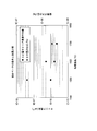
- FIG. 1A shows four types of carbon-based materials coated with TaC in a normal production cycle without performing a purification process (vacuum baking) in the conventional SiC epitaxial wafer manufacturing apparatus shown in FIG. SiC epitaxial fabricated using the following members (the susceptor 24, the satellite 26, the ceiling 22, the exhaust string 23, and if there are small parts attached to the above members, they are included in the above members and considered as one unit) It is the graph which showed transition of the carrier concentration (carrier concentration in a SiC epitaxial film) in a wafer.
- the vertical axis represents the carrier concentration of the SiC epitaxial wafer, and the horizontal axis represents the integrated heating time (the integrated time of heating accompanying epi growth).
- the transition of the carrier concentration background (carrier concentration in epitaxial growth performed without intentional doping) up to 2 months after the replacement of the four types of TaC-coated carbon-based material members is 0 hours. Yes.
- the plots of ⁇ and ⁇ and the broken line represent the carrier concentration.
- the difference between the plots ⁇ and ⁇ is only the difference in the thickness of the epitaxial film, and the thickness is in the relationship ⁇ ⁇ .
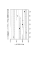
- FIG. 1B shows a transition image of changes in the surface defect density in the SiC epitaxial film due to downfall.
- the downfall means that deposits deposited on the inner wall portion in the apparatus become particles generation sources and fly during the epitaxial growth process, are taken into the epitaxial growth film, and become defects.
- the horizontal axis of FIG. 1 (a) and FIG. 1 (b) is common, and is an integrated heating time starting from when the graphite member in the reactor is replaced with a new one.
- This cumulative heating time is the time for epitaxial growth (including the case where baking is performed under the same heating conditions (temperature and degree of vacuum) as for epitaxial growth).
- the degree of vacuum is a pressure condition that is higher than the degree of vacuum used in the vacuum baking furnace of the present application in a reduced pressure state of about 10 4 Pa that is usually used during epitaxial growth of SiC.
- the background of the carrier concentration rapidly decreases from the replacement of the member until the accumulated heating time is about 100 hours, and is stabilized thereafter.
- This background carrier concentration is not related to the growth film thickness obtained by one epitaxial growth, and the tendency is not affected even if doping epitaxial growth (not plotted in the figure) is interposed. That is, the background carrier concentration is almost determined by the accumulated heating time.
- the surface defects caused by the downfall become unstable after the heating time of about 500 hours and show an increasing tendency, and finally increase rapidly.
- the absolute amount of deposit deposited in the apparatus increases by repeating the film formation, and the deposit deposit re-flys on the wafer surface as particles during film formation, increasing the density of downfall, It is thought that the TaC coat deteriorates and peels from the member together with the deposits.
- SiC epitaxial wafers are 1.2 ⁇ 10 15 cm ⁇ 3 or less (line A shown in FIG. 1) for high-voltage products, and 1.0 ⁇ 10 16 cm ⁇ 3 or less for normal products (shown in FIG. 1).
- Line B) is a general-purpose product and should have a carrier concentration background of 1.1 ⁇ 10 16 cm ⁇ 3 or less (line C shown in FIG. 1).
- the SiC epitaxial wafer cannot be used as a normal product.
- the upper limit of the period during which the member can be used is limited with respect to the accumulated heating time.
- the SiC epitaxial wafer manufacturing apparatus cannot manufacture an epitaxial wafer for a certain period after the replacement of the member, and has taken measures to accumulate the integrated heating time by performing baking or dummy epitaxial growth.
- each member of the epitaxial growth apparatus is used for baking, it is performed under the same temperature and pressure conditions as the epitaxial growth because of restrictions on the apparatus and the influence on the subsequent epitaxial growth.
- the heat treatment using this epitaxial growth apparatus has been a production loss as an operation time during which the entire period does not contribute to production.
- the member since the member has a limitation on the accumulated heating time that can be used from the viewpoint of an increase in surface defects caused by particles, the production loss for stabilizing the background carrier concentration is a very big problem. there were.
- the production loss has been considered as a necessary cost for manufacturing a SiC epitaxial wafer in the field, and the present inventor is not aware of other studies for drastically eliminating it.
- the manufacturing method of the SiC epitaxial wafer of this invention eliminates this production loss drastically.
- a coated carbon-based material member is used.
- the gas contained in the member can be degassed as compared to a solid uncoated member. difficult.
- the present inventor has found that the nitrogen content of the coated carbon-based material member may be sufficiently degassed, and the conditions for the vacuum baking. It was found that the degassing effect can be maintained even if the coated carbon-based material member is sufficiently degassed with nitrogen and then exposed to a nitrogen-containing atmosphere.
- the coated carbon-based material member of the present invention can be degassed by baking under certain conditions even if it is coated, and even if the member is exposed to a nitrogen-containing atmosphere (air), it is substantially due to re-adsorption. This is based on the new finding that there is no adverse effect of nitrogen.
- a dedicated vacuum baking furnace separate from the SiC epitaxial wafer production apparatus is used in order to eliminate the production loss. Then, using the dedicated vacuum baking furnace, degassing (purification treatment) is performed under predetermined vacuum baking conditions.
- the degree of vacuum when vacuum baking is performed in a dedicated baking furnace is 2.0 ⁇ 10 ⁇ 3 Pa or less.
- the degree of vacuum is preferably 1.0 ⁇ 10 ⁇ 4 Pa or less, more preferably 1.0 ⁇ 10 ⁇ 5 Pa or less, and further preferably 1.0 ⁇ 10 ⁇ 6 Pa or less. 1.0 ⁇ 10 ⁇ 7 Pa or less is even more preferable.
- the lower limit is not particularly limited, but in order to obtain a degree of vacuum higher than 1.0 ⁇ 10 ⁇ 8 , the exhaust device becomes expensive, so a pressure higher than that is preferable.
- a vacuum device such as a turbo molecular pump or a QMS (quadrupole mass spectrometer) can be stably operated.
- a dry pump or the like is often used.
- vacuum baking is performed at a vacuum higher than a high vacuum in order to desorb inclusion nitrogen from the coated carbonaceous material member. ing.
- the degree of vacuum at the time of vacuum baking performed in the present invention is equal to or higher than the degree of vacuum that can be achieved only by a dry pump, and a turbo molecular pump or an ion getter pump that can achieve the degree of vacuum is used.
- the temperature at the time of vacuum baking is preferably 1400 ° C or higher, more preferably 1500 ° C or higher, and further preferably 1600 ° C or higher. If it is 1400 ° C. or lower, it takes a very long time until the amount of nitrogen contained is sufficiently desorbed. Temperatures above 1700 ° C cannot be easily achieved with normal inexpensive resistance heating. Therefore, it is preferable that the temperature is 1700 ° C. or less from the viewpoint of cost and the like. If the temperature is too high, a member coated with SiC may crack and peel off the coating, making it unusable. Heating at 1400 ° C. or higher can be realized by using generally used materials such as high-frequency heating in addition to resistance heating.
- the vacuum baking time is preferably 10 hours or more.
- the nitrogen gas partial pressure detected by the quadrupole mass spectrometer (QMS) decreases to 1/2 to 1/8 of the initial value, and the nitrogen contained therein is sufficiently desorbed. This is because it can be considered.
- From the viewpoint of enhancing the effect of nitrogen degassing it is more preferably 20 hours or more, and more preferably 30 hours or more. More preferably, it is more preferable to set the time longer than that.
- vacuum baking may be performed with the time determined from the viewpoint of productivity as the upper limit.
- the upper limit may be 100 hours, 150 hours, 200 hours, or the like.
- the vacuum baking is preferably performed until the nitrogen partial pressure becomes 1.0 ⁇ 10 ⁇ 7 Pa or less. If it is 1.0 ⁇ 10 ⁇ 7 Pa or less, the background becomes sufficiently low to use the SiC wafer as the SiC semiconductor device.
- the nitrogen partial pressure can be measured with a QMS (quadrupole mass spectrometer).
- the coated carbon material member is preferably coated with a thickness of 10 to 50 ⁇ m on the surface of the carbon material.
- a thickness of 10 to 50 ⁇ m When it is less than 10 ⁇ m, the initial particle size of the coating material is small and the surface of the graphite material cannot be sufficiently covered. Therefore, re-entry of nitrogen gas that has been desorbed after the purification treatment occurs. If it exceeds 50 ⁇ m, cracks on the coating surface are likely to occur, and the member life is shortened.
- FIG. 2 shows an optical micrograph of a member having a graphite surface coated with a 20 ⁇ m thick TaC film. As shown in FIG. 2, it can be seen that grains having a diameter of about 20 ⁇ m are formed by aggregation. Each grain is arranged without a gap and covers the surface of the graphite, and this coating improves the durability of the member.
- this coating densely covers the surface of the carbon-based material member, it prevents desorption of nitrogen gas contained in the member by vacuum baking. For this reason, it is difficult to sufficiently desorb the nitrogen gas at a vacuum level (1 Pa to several hundred Pa) that is generally used for a dry pump, which is not efficient.
- desorption of nitrogen gas in a short time can be realized by carrying out in a high vacuum environment.
- the coated carbon-based material member can be taken out into the atmosphere.
- nitrogen in the atmosphere will be reabsorbed into the member.
- the surface of the carbon-based material member is densely protected by coating, so that even if the carbon-based material member is taken out into the atmosphere, the contained nitrogen can be kept small. That is, the vacuum-baked carbon-based material member can be stocked in the atmosphere.
- coated carbon-based material member for example, a carbon-based material member coated with SiC or TaC, which is generally used for epitaxial growth, can be used.
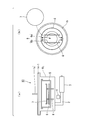
- FIG. 3 is a schematic view showing an example of a dedicated baking furnace used in the present invention, where (a) is a sectional view and (b) is a plan view.
- the dedicated baking furnace used in the present invention is, for example, a dedicated baking furnace 10 as shown in FIGS. 3A and 3B, and includes a SUS chamber 1, an exhaust line 2 connected from the chamber 1, a dry pump, It has an exhaust system 3 composed of a turbo molecular pump and a quadrupole mass spectrometer (QMS) 4 for analyzing nitrogen gas during exhaust.
- the inside of the SUS chamber 1 can be exhausted and depressurized from the exhaust line 2 by the exhaust facility 3.
- the SUS chamber 1 includes a lid portion 1a, a main body portion 1b, and a flange portion 1c, and has a flow path through which flowing water flows for cooling (not shown).
- the lid portion 1a and the main body portion 1b are in close contact with an O-ring or the like in order to prevent air from entering during evacuation.
- the flange portion 1c includes a gas introduction nozzle and a radiation thermometer monitor port at the center (not shown). Inside the chamber, there are a heat shield plate 5, a heater 6, a tray 7, and a rail 8 for holding the tray.
- the heat shield plate 5 is made of a laminate of 10 or more high melting point metal plates, and is provided to thermally shut the inside and outside of the furnace that becomes high temperature and keep the inside of the chamber 1 at a constant temperature. .
- the heater 6 is made of graphite and is a resistance heating type heater. In the case of the resistance heating method, it is possible to realize the temperature up to about 1700 ° C.
- the heater 6 is divided into two regions, an IN-side heater 6a and an OUT-side heater 6b, and corresponds to the soaking of the atmosphere in the furnace.
- the tray 7 is made of graphite, on which a coated carbon-based material member for an epitaxial wafer manufacturing apparatus is placed.
- the tray 7 is placed almost horizontally on the rail 8 for holding the tray.
- the temperature of the tray 7 can be monitored by a monitor port for a radiation thermometer installed on the flange portion 1c.
- the exhaust facility 3 is composed of a dry pump and a turbo molecular pump, and can generally achieve a high vacuum degree of about 10 ⁇ 1 to 10 ⁇ 6 Pa.
- vacuuming is performed with a dry pump level, and vacuuming is not performed with a turbo molecular pump and a dry pump.
- vacuum baking is performed by pulling up to a high vacuum by using such exhaust equipment.
- the air in the chamber whose pressure has been reduced by the exhaust facility 3 passes through the quadrupole mass spectrometer (QMS) 4 installed in the exhaust line simultaneously when passing through the exhaust line 2. At this time, it is possible to periodically monitor the desorption level of the nitrogen gas by analyzing the degassed component being exhausted and its partial pressure.
- QMS quadrupole mass spectrometer
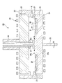
- FIG. 4 is a schematic cross-sectional view showing an example of an epitaxial wafer manufacturing apparatus used in the present invention.
- the epitaxial wafer manufacturing apparatus used in the present invention is, for example, a CVD (Chemical Vapor Deposition) apparatus 20 as shown in FIG. While supplying the gas G, a film (not shown) is deposited and grown on the surface of the heated wafer W.
- the source gas G may be one containing silane (SiH 4 ) as the Si source and propane (C 3 H 8 ) as the carbon (C) source, and hydrogen ( Those containing H 2 ) can be used.
- FIG. 4 shows the structure of the main part inside the reactor, and these are stored in a SUS chamber (not shown) that can be evacuated.
- the CVD apparatus 20 includes a mounting plate 21 on which a plurality of wafers W are placed and a reaction space K between the mounting plate 21 and the mounting plate 21.
- a ceiling (top plate) 22 disposed opposite to the upper surface and an exo string 23 disposed outside the mounting plate 21 and the ceiling 22 so as to surround the reaction space K are provided.
- the exostring 23 forms a peripheral wall with respect to the reaction space K, and has a structure in which the carrier gas is exhausted from the reaction space K through a plurality of holes (exhaust holes) formed in the exostring 23.
- the mounting plate 21 includes a disc-shaped susceptor (rotary base) 24 and a rotating shaft 25 attached to the central portion of the susceptor lower surface 24b.
- the susceptor 24 is rotatably supported integrally with the rotating shaft 25.
- the cover disk can prevent the SiC deposit from adhering directly to the susceptor 24.
- the cover disk is included in the susceptor unit as a part accompanying the susceptor.
- a plurality of concave accommodating portions 27 for accommodating satellites (disk-shaped wafer support bases) 26 on which the wafer W is placed are provided.
- the accommodating portions 27 have a circular shape in a plan view (as viewed from the susceptor upper surface 24a side), and a plurality of the accommodating portions 27 are provided at equal intervals in the circumferential direction (rotational direction) of the susceptor 24. In FIG. 4, the case where the six accommodating parts 27 are provided along with equal intervals is illustrated.
- the satellite 26 has an outer diameter slightly smaller than the inner diameter of the accommodating portion 27 of the susceptor 24, and is supported from below by a pin-like small protrusion (not shown) at the center of the bottom surface of the accommodating portion 27.
- the housing 27 of the susceptor 24 is supported so as to be rotatable around each central axis.
- the upper surface of the wafer W after placing the wafer is on the same plane as the susceptor upper surface 24a or on the lower side thereof.
- the material gas flow disturbance laminar flow disturbance
- a satellite unit may be configured by arranging a ring as shown in the figure on the outer periphery of the satellite upper surface and fixing the wafer to the center of the satellite.
- the mounting plate 21 adopts a so-called planetary (automatic revolution) system.
- the rotation shaft 25 is rotationally driven by a drive motor (not shown)
- the mounting plate 21 is rotationally driven around its central axis.
- the plurality of wafer support tables 26 are driven to rotate around their respective central axes by supplying a driving gas different from the source gas between the lower surface of each satellite 26 and the accommodating portion. (Not shown). Thereby, it is possible to form a film evenly on each of the wafers W placed on the plurality of wafer support tables 26.
- the sealing 22 is a disk-shaped member having a diameter substantially coincident with the susceptor 24 of the mounting plate 21, and forms a flat reaction space K between the mounting plate 21 and the upper surface of the susceptor 24.
- the exo string 23 is a ring-shaped member that surrounds the outer peripheries of the mounting plate 21 and the ceiling 22. The exo string 23 allows the reaction space K to communicate with the exhaust space on the outside through a plurality of holes (shown as through holes at both ends in the figure).
- the CVD apparatus 20 includes an induction coil 29 for heating the mounting plate 21 and the ceiling 22 by high frequency induction heating as a heating means for heating the wafer W placed on the satellite 26.
- the induction coil 29 is disposed to face the lower surface of the mounting plate 21 (susceptor 24) and the upper surface of the ceiling 22 in a state of being close to each other.
- this CVD apparatus 20 when a high frequency current is supplied from a high frequency power supply (not shown) to the induction coil 29, the mounting plate 21 (susceptor 24 and satellite 26) and the ceiling 22 are heated by high frequency induction heating.
- the wafer W placed on the satellite 26 can be heated by radiation from the 21 and the ceiling 22, heat conduction from the satellite 26, or the like.
- a material made of a graphite (carbon) material having excellent heat resistance and good thermal conductivity is used as a material suitable for high-frequency induction heating. Further, in order to prevent generation of particles from graphite (carbon), a material whose surface is coated with SiC, TaC or the like can be preferably used.
- the graphite mounting plate 21 (susceptor 24 and satellite 26) and the ceiling 22 contain nitrogen, and this nitrogen serves as a dopant for a compound semiconductor such as a SiC semiconductor, and thus a manufactured SiC device.
- by performing the vacuum baking in a dedicated baking furnace it is possible to eliminate the occupation time of the epitaxial wafer manufacturing apparatus by vacuum baking and to significantly reduce the time required for the vacuum baking.
- the heating means is not limited to the above-described high-frequency induction heating, but may be resistance heating. Further, the heating means is not limited to the configuration disposed on the lower surface side of the mounting plate 21 (susceptor 24) and the upper surface side of the ceiling 22, but may be configured only on either one of these. .
- the CVD apparatus 20 includes a gas introduction pipe (gas introduction port) 30 for introducing the source gas G into the reaction space K from the center of the upper surface of the ceiling 22 as a gas supply means for supplying the source gas G into the chamber.
- the gas introduction pipe 30 is formed in a cylindrical shape and penetrates through a support ring 31 having a circular opening provided at the center of the ceiling 22, and its tip (lower end) is a reaction space K. It is arranged facing the inside.
- the flange part 30a which protruded in the diameter expansion direction is provided in the front-end
- the flange portion 30 a is for causing the raw material gas G released vertically downward from the lower end portion of the gas introduction pipe 30 to flow radially between the opposing susceptors 24.
- the source gas G released from the gas introduction pipe 30 is caused to flow radially from the inside to the outside of the reaction space K, so that the source gas G is parallel to the in-plane of the wafer W. It is possible to supply. Gas that is no longer necessary in the chamber can be discharged out of the chamber through an exhaust hole provided in the exhaust string 23.
- the sealing 22 is heated by the induction coil 29 at a high temperature, but the inner peripheral portion (the central portion supported by the support ring 31) has a low temperature for introducing the raw material gas G. 30 is not contacted. Further, the sealing 22 is supported vertically upward by placing the inner peripheral portion thereof on a support ring (support member) 31 attached to the outer peripheral portion of the gas introduction pipe 30. Further, the ceiling 22 can be moved in the vertical direction.
- FIG. 5 shows a SiC epitaxial wafer when a SiC epitaxial film is formed by using a coated carbon-based material member that has been actually vacuum-baked and a carbon-based material member that has not been vacuum-baked. The transition of the carrier concentration background is shown.
- a planetary type SiC-CVD growth apparatus manufactured by Aixtron as shown in FIG. 4 was used as the SiC epitaxial wafer manufacturing apparatus.
- the coated carbon-based material member includes a susceptor unit (reference numeral 24 in FIG. 4), a satellite unit (reference numeral 26 in FIG. 4), a sealing unit (reference numeral 22 in FIG. 4), and an exo string unit (FIG. 4).
- the coating was a TaC coating having a thickness of 20 ⁇ m.
- the vacuum baking was performed at 1500 ° C. for 200 hours using a dedicated baking furnace.
- the epitaxial growth of SiC was performed at 1500 to 1550 ° C., H 2 was used as a carrier gas, and the atmospheric pressure was 100 to 200 mmbar.
- the TaC-coated carbon-based material member that has not been vacuum-baked (“epi with no baking” in the legend of FIG. 5) was formed even when the cumulative heating time (the cumulative time of epi growth) passed about 70 hours.
- the SiC wafer has a carrier concentration background of 1.1 ⁇ 10 16 cm ⁇ 3 or more, and general-purpose wafers cannot be produced.
- a TaC-coated carbon-based material member that has been vacuum-baked (described as a baking furnace purification member) has a normal product specification (1) with an integrated heating time of about 3 hours (6 ⁇ m epitaxial growth for 2 cycles). Wafers of 0.0 ⁇ 10 16 cm ⁇ 3 or less) can be produced. Further, although not shown in FIG.
- a wafer with a high breakdown voltage specification (1.2 ⁇ 10 15 cm ⁇ 3 or less) can be produced in about one week.
- a TaC-coated carbon-based material member that has not been vacuum-baked requires about a month.
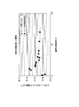
- FIG. 6 shows a molecular weight 28 monitored by a quadrupole mass spectrometer (QMS) when a set of TaC-coated carbon-based material members (the above-mentioned four types of members) was processed at different temperatures during vacuum baking. It is the figure which showed gas (nitrogen) partial pressure.
- the vacuum baking temperature was 1500 ° C., 1600 ° C., and 1700 ° C., respectively, and was performed for up to 200 hours.
- 1600 degreeC and 1700 degreeC performed the thing of 100 hours.
- the one at 1600 ° C is 200 hours and the nitrogen gas partial pressure when the temperature is lowered to 1500 ° C after the end of 100 hours is 200 hours at 1700 ° C.
- 1700 ° C. (100 h) 1600 ° C. measurement is a value obtained by measuring the nitrogen gas partial pressure when the temperature is lowered to 1600 ° C. after vacuum baking at 1700 ° C. for 100 hours. Show.
- FIG. 6 shows that the treatment time becomes longer under all conditions and the nitrogen partial pressure decreases. Comparing the nitrogen partial pressure measured in a state where the temperature was lowered to the same temperature (1500 ° C.) after vacuum baking, the higher the baking temperature, the lower the final nitrogen partial pressure. Moreover, the final nitrogen partial pressure measured at the same temperature is less when the vacuum baking is performed at 1700 ° C. for 100 hours than when the vacuum baking is performed at 1600 ° C. for 200 hours, and the vacuum baking time is lengthened. It can be seen that increasing the temperature is more effective.
- Step bunching refers to a phenomenon in which atomic steps (usually about 2 to 10 atomic layers) gather and coalesce on the surface, and sometimes refers to the surface step itself.
- an example of the step bunching free condition is disclosed in, for example, Japanese Patent No. 4959763 and Japanese Patent No. 4887418.
- the ultimate vacuum when treated at 1500 ° C. and 1600 ° C. for the same time is 1.01 ⁇ 10 ⁇ 5 Pa, 1.19 ⁇ 10 ⁇ 5 Pa and the nitrogen gas content measured at 1500 ° C., respectively.
- the pressures were 3.89 ⁇ 10 ⁇ 8 Pa and 7.12 ⁇ 10 ⁇ 9 Pa, respectively.
- the obtained carrier concentration background was 1.02 ⁇ 10 16 cm ⁇ 3 and 8.51 ⁇ 10 15 cm ⁇ 3 . From this, the higher the treatment temperature, the smaller the nitrogen gas partial pressure and the better the carrier concentration background.
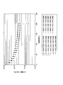
- FIG. 7 shows an epitaxial wafer manufacturing apparatus after vacuum baking is performed on each of the above four types of members as TaC-coated carbon-based material members in a SiC epitaxial wafer manufacturing apparatus under various conditions. This is a result of measuring the background of the carrier concentration by preparing an SiC epitaxial film by undoping and measuring the background of the carrier concentration.
- (A) to (g) in FIG. 7 are values when (a) the member is not vacuum-baked (initial state), (b) are target values immediately after replacement of the member, and (c) A value obtained when all four types of carbon material members coated in a planetary type SiC-CVD growth apparatus manufactured by Aixtron are vacuum-baked at 1500 ° C. for 100 hours, and (d) coated carbon This is the value when all four types of members composed of carbonaceous material members are vacuum-baked at 1500 ° C. for 200 hours, and (e) all four types of members composed of coated carbon-based material members are treated at 1600 ° C. for 200 hours.
- (G) is a value when the four members set all made of coated carbonaceous material member was 200 hours vacuum baking at 1700 ° C.. These are the background carrier concentrations obtained in the first SiC epitaxial growth after each condition vacuum baking in a dedicated vacuum baking furnace using a new set of members.
- FIG. 8 shows a case where a TaC-coated carbon-based material member is subjected to vacuum baking at 1700 ° C. under conditions of 1.4 ⁇ 10 ⁇ 4 Pa at the start and 3.6 ⁇ 10 ⁇ 5 Pa at the end.
- the measurement result of gas partial pressure is shown.
- the “member set 1”, “member set 2”, “member set 3”, and “member set 4” in the legend of FIG. 8 have four types of members (susceptor 24, satellite 26, sealing 22, extrude string 23, and the above-described members). If there are small parts attached to the above, they are included in the above members and considered as one unit). Therefore, FIG. 8 shows the result of measuring the change in the nitrogen gas partial pressure when four sets of four members are prepared and vacuum baking is performed.
- the degree of vacuum and the nitrogen partial pressure when baking is started at 1700 ° C. vary depending on the member, the ultimate degree of vacuum after processing after performing vacuum baking for a certain time tends to converge to a certain level. This is because new TaC-coated carbon-based material members vary in the amount of nitrogen released depending on the history of their materials and storage conditions, but this variation can be achieved by performing vacuum baking over a certain condition. This indicates that the variation in the carrier concentration of the SiC epitaxial layer caused by the variation in the initial state of the TaC-coated carbon-based material member can be reduced.
- the vacuum baking time for which a remarkable effect starts to appear is 10 hours or more. This is because it is considered that the QMS detection nitrogen gas partial pressure is reduced to 1/2 to 1/4 in the first 10 hours, and the carrier concentration background is sufficiently lowered. Furthermore, in order to eliminate the initial variation of the members, it is more preferable to perform a vacuum baking process time of 100 hours or more.
- FIG. 9 shows the background of the carrier concentration of the SiC epitaxial growth layer, the vacuum baking temperature dependence of the TaC-coated carbon-based material member (the above four types of members), and the final measurement measured at 1500 ° C. after the vacuum baking. It is a graph which shows nitrogen partial pressure.
- the degree of vacuum of the vacuum baking was 1.0 ⁇ 10 ⁇ 5 Pa, and the time was 200 hours. As a result, it can be seen that the final nitrogen gas partial pressure decreases as the temperature rises, the background of the carrier concentration of the SiC epitaxial growth layer decreases correspondingly, and a good film is formed.
Landscapes
- Chemical & Material Sciences (AREA)
- Engineering & Computer Science (AREA)
- Materials Engineering (AREA)
- Metallurgy (AREA)
- Organic Chemistry (AREA)
- Chemical Kinetics & Catalysis (AREA)
- General Chemical & Material Sciences (AREA)
- Crystallography & Structural Chemistry (AREA)
- Inorganic Chemistry (AREA)
- Mechanical Engineering (AREA)
- Chemical Vapour Deposition (AREA)
- Crystals, And After-Treatments Of Crystals (AREA)
Abstract
Description
例えば、炭化珪素(SiC)は、シリコン(Si)に対して、バンドギャップが約3倍、絶縁破壊電界強度が約10倍、熱伝導度が約3倍という優れた物性を有しており、パワーデバイス、高周波デバイス、高温動作デバイス等への応用が期待されている。
SiCのエピタキシャル成長は、1500℃以上の高温で行われる。そのため、エピタキシャルウェハの製造装置の部材としては、耐熱性に優れ、なおかつ熱伝導率の良いグラファイト(カーボン)材料や、グラファイト基材の表面をTaC等でコーティングされたものが一般に使用されている。
特許文献1には、SiCエピタキシャルウェハの製造装置内において、エピタキシャル成長前にグラファイトサセプタを真空ベークすることで、グラファイトサセプタ内に内包する窒素を低減すること、及び、内包する窒素低減後のグラファイトサセプタの表面にSi及びSiCの少なくとも一方の被膜をコートすることが開示されている。特許文献2には、ハロゲンガス雰囲気下で炭素系材料を圧力100Pa以下、1800℃以上で熱処理し、炭素系材料中の窒素を放出させた後、希ガス雰囲気下で室温まで冷却する低窒素濃度炭素系材料の製造方法が開示されている。特許文献3には、ウェハを載置する部分の少なくとも一部が炭化タンタル又は炭化タンタル被覆黒鉛材であるサセプタが開示されている。
また、ウェハを装置内に出し入れする際にも、環境をグローブボックスのようなAr環境中に置く、又は一度ロードロック室等でAr置換処理後に炉内に搬送することで、窒素ガスの炉内への持ち込みを極力抑制し、無垢の炭素系材料部材への窒素ガスの再付着および侵入を防ぐ必要があった。
ここで、キャリア濃度バックグラウンドとは、新品の炭素系材料部材をエピタキシャルウェハ製造装置に装着し、SiCエピタキシャル膜をアンドープで作製した際のSiCのキャリア濃度を意味する。
そのため、生産現場では、エピタキシャルウェハ製造装置内で1週間程度のエージング処理(真空ベーク)が行われてきた。この間、製品(エピタキシャルウェハ)の製造を行うことができなくなり、生産効率が著しく落ちてしまうという問題があった。
(1)コーティングされた炭素系材料部材を、専用の真空ベーク炉において2.0×10⁻³Pa以下の真空度で真空ベークする工程と、前記コーティングされた炭素系材料部材を、エピタキシャルウェハ製造装置に設置する工程と、前記エピタキシャルウェハ製造装置内にSiC基板を配置し、そのSiC基板上にSiCエピタキシャル膜をエピタキシャル成長させる工程と、を有するSiCエピタキシャルウェハの製造方法。
(2)前記真空度が1.0×10⁻⁵Pa以下であることを特徴とする(1)に記載のSiCエピタキシャルウェハの製造方法。
(3)前記真空ベークを1400℃以上の温度で行うことを特徴とする(1)又は(2)のいずれかに記載のSiCエピタキシャルウェハの製造方法。
(4)前記真空ベークを10時間以上行うことを特徴とする(1)~(3)のいずれか一つに記載のSiCエピタキシャルウェハの製造方法。
(5)前記真空ベークを、1500℃での窒素分圧が1.0×10⁻⁷Pa以下になるまで行うことを特徴とする(1)~(4)のいずれか一つに記載のSiCエピタキシャルウェハの製造方法。
(6)前記コーティングされた炭素系材料部材が、サセプタ、サテライト、シーリング、イグゾーストリング、からなる群から選択されたいずれかを含むことを特徴とする(1)~(5)のいずれか一つに記載のSiCエピタキシャルウェハの製造方法。
(7)前記コーティングが、TaCまたはSiCを用いてなされていることを特徴とする(1)~(6)のいずれか一つに記載のSiCエピタキシャルウェハの製造方法。
専用のベーク炉とは、エピタキシャル膜を成長させる工程に用いる炉とは別に、所定条件のベーキングを行うために用意される炉のことである。「専用の」とは特定の炉の構造を指すものではない。
「炭素系材料部材」における炭素系材料は、グラファイト、パイロリティックグラファイト等の炭素(カーボン)を主成分とする材料全般を意味する。すなわち、カーボン材料、炭素材料等の名称で特定される材料全般を意味する。
縦軸はSiCエピタキシャルウェハのキャリア濃度であり、横軸は積算加熱時間(エピ成長に伴う加熱の積算時間)である。上記4種類のTaCコーティングされた炭素系材料部材の交換直後を0時間とし、2ヵ月後までのキャリア濃度バックグラウンド(故意のドーピングを行わないで実施したエピタキシャル成長でのキャリア濃度)の推移を示している。図1(a)において、◇と□のプロット及び破線がキャリア濃度を表している。プロット◇と□の違いは、エピタキシャル膜の厚さが違うだけであり、その厚さは◇<□の関係である。
また、ダウンフォールに起因する表面欠陥があるエピタキシャルウェハは製品とはならないため、当該部材が使用できる期間は、積算加熱時間に対して上限が限られている。
生産現場では当該部材交換後一定期間は、SiCエピタキシャルウェハ製造装置においてはエピタキシャルウェハの製造を行うことができず、ベーキングやダミーエピタキシャル成長を行って積算加熱時間を累積させる対応を取っていた。エピタキシャル成長装置の各部材をベーキングに用いる場合、装置上の制約及びその後のエピタキシャル成長への影響から、エピタキシャル成長と同様の温度や圧力の条件で行われる。このエピタキシャル成長装置を用いた加熱処理は、その期間が全て生産に寄与しない稼働時間として、生産ロスとなっていた。当該部材は、上述のように、パーティクルに起因する表面欠陥の増加の点から、使用できる積算加熱時間の制約があるため、このバックグラウンドキャリア濃度の安定化のための生産ロスは極めて大きな問題であった。
本発明のSiCエピタキシャルウェハの製造方法は、かかる生産ロスを抜本的に解消するものである。
本発明者は、コーティングされた炭素系材料部材について、内包する窒素の脱ガスが十分になされる場合があること、そして、その真空ベークの条件を見出したのである。そして、コーティングされた炭素系材料部材について一旦、十分に窒素の脱ガスした後、窒素含有雰囲気に晒しても、脱ガスの効果を維持できることを見出したのである。本発明のコーティングされた炭素系材料部材は、コーティングされていても一定条件のベーキングで脱ガスすることが出来、かつ部材を窒素含有雰囲気(空気)にさらしても、実質的には再吸着による窒素の悪影響がないという新たな知見に基づくものである。
1.0×10⁻⁷Pa以下であれば、SiCウェハをSiC半導体デバイスとして使用するために十分低いバックグラウンドとなる。窒素分圧は、QMS(4重極質量分析装置)で測定することができる。
図2は、グラファイト表面に厚さ20μmのTaC膜をコーティングされた部材の光学顕微鏡写真を示す。図2に示すように、直径20μm程度のグレインが凝集して形成されていることが分かる。それぞれのグレインは隙間なく配列して、グラファイト表面を覆っており、このコーティングにより部材の耐久性を向上させている。
また専用ベーク炉からSiCエピタキシャル製造装置へ搬送する際に、周囲の環境を考慮に入れる必要もない。
図3は、本発明で用いられる専用ベーク炉の一例を示す模式図であり、(a)は断面図であり、(b)は平面図である。
本発明で用いられる専用ベーク炉は、例えば、図3(a)(b)に示すような専用ベーク炉10であり、SUS製のチャンバー1と、チャンバー1から繋がる排気ライン2と、ドライポンプ及びターボ分子ポンプからなる排気設備3と、排気時の窒素ガスを分析するための4重極質量分析装置(QMS)4とを有する。排気ライン2から排気設備3によって、SUS製チャンバー1内を排気減圧することが可能である。
図4は、本発明で用いられるエピタキシャルウェハ製造装置の一例を示す断面模式図である。
本発明で用いられるエピタキシャルウェハ製造装置は、例えば、図4に示すようなCVD(化学的気相成長)装置20であり、図示を省略する減圧排気可能なチャンバー(成膜室)内に、原料ガスGを供給しながら、加熱されたウェハWの面上に膜(図示せず。)を堆積成長させるものである。例えば、SiCをエピタキシャル成長させる場合、原料ガスGには、Si源にシラン(SiH4)、炭素(C)源にプロパン(C3H8)を含むものを用いることができ、キャリアガスとして水素(H2)を含むものを用いことができる。図4は、リアクター内部の主要部分の構成を図示したものであり、これらは減圧排気可能なSUS製のチャンバー(図示せず)の中に納められる形になっている。
また、サセプタ上面24a側には、ウェハWが載置されるサテライト(円盤状のウェハ支持台)26を収容する複数の凹状の収容部27が設けられている。
1700℃でベーキングを開始した時の真空度や窒素分圧は、部材によって差がみられるが、一定時間真空ベーキングを行った処理後の到達真空度は一定のレベルに収束する傾向がある。これは、新品のTaCコーティングされた炭素系材料部材は、その材料や保管状態などの履歴により、放出する窒素の量がばらついているが、一定条件以上の真空ベーキングを行うことにより、そのばらつきを解消することができ、TaCコーティングされた炭素系材料部材の初期状態のばらつきに起因していたSiCエピタキシャル層のキャリア濃度のばらつきを低減させることができることを示している。
真空ベークの真空度は1.0×10⁻⁵Paで、時間はそれぞれ200時間行った。その結果、温度が上昇するほど最終的な窒素ガス分圧は減少し、それに対応してSiCエピタキシャル成長層のキャリア濃度のバックグラウンドは下がり、良好な膜が成膜されていることが分かる。
1a 蓋部、
1b 本体部、
1c フランジ部、
2 排気ライン、
3 排気設備、
4 4重極質量分析装置(QMS)、
5 遮蔽板、
6 ヒーター、
6a IN側ヒーター、
6b OUT側ヒーター、
7 トレー、
8 レール、
10 専用ベーク炉、
20 CVD(化学的気相成長)装置、
21 搭載プレート、
22 シーリング、
23 イグゾーストリング、
24 サセプタ、
25 回転軸、
26 サテライト、
27 収容部、
29 誘導コイル、
30 ガス導入管、
30a フランジ部、
31 支持リング、
W ウェハ、
G 原料ガス
Claims (7)
- コーティングされた炭素系材料部材を、専用の真空ベーク炉において2.0×10⁻³Pa以下の真空度で真空ベークする工程と、
前記コーティングされた炭素系材料部材を、エピタキシャルウェハ製造装置に設置する工程と、
前記エピタキシャルウェハ製造装置内にSiC基板を配置し、そのSiC基板上にSiCエピタキシャル膜をエピタキシャル成長させる工程と、を有するSiCエピタキシャルウェハの製造方法。 - 前記真空度が1.0×10⁻⁵Pa以下であることを特徴とする請求項1に記載のSiCエピタキシャルウェハの製造方法。
- 前記真空ベークを1400℃以上の温度で行うことを特徴とする請求項1又は2のいずれかに記載のSiCエピタキシャルウェハの製造方法。
- 前記真空ベークを10時間以上行うことを特徴とする請求項1~3のいずれか一項に記載のSiCエピタキシャルウェハの製造方法。
- 前記真空ベークを、1500℃での窒素分圧が1.0×10⁻⁷Pa以下になるまで行うことを特徴とする請求項1~4のいずれか一項に記載のSiCエピタキシャルウェハの製造方法。
- 前記コーティングされた炭素系材料部材が、サセプタ、サテライト、シーリング、イグゾーストリングからなる群から選択されたいずれかを含むことを特徴とする請求項1~5のいずれか一項に記載のSiCエピタキシャルウェハの製造方法。
- 前記コーティングが、TaCまたはSiCを用いてなされていることを特徴とする請求項1~6のいずれか一項に記載のSiCエピタキシャルウェハの製造方法。
Priority Applications (2)
| Application Number | Priority Date | Filing Date | Title |
|---|---|---|---|
| US14/913,865 US20160208414A1 (en) | 2013-09-04 | 2014-08-13 | METHOD FOR PRODUCING SiC EPITAXIAL WAFER |
| CN201480042773.4A CN105408985B (zh) | 2013-09-04 | 2014-08-13 | SiC外延晶片的制造方法 |
Applications Claiming Priority (2)
| Application Number | Priority Date | Filing Date | Title |
|---|---|---|---|
| JP2013-183373 | 2013-09-04 | ||
| JP2013183373A JP6226648B2 (ja) | 2013-09-04 | 2013-09-04 | SiCエピタキシャルウェハの製造方法 |
Publications (1)
| Publication Number | Publication Date |
|---|---|
| WO2015033752A1 true WO2015033752A1 (ja) | 2015-03-12 |
Family
ID=52628232
Family Applications (1)
| Application Number | Title | Priority Date | Filing Date |
|---|---|---|---|
| PCT/JP2014/071380 Ceased WO2015033752A1 (ja) | 2013-09-04 | 2014-08-13 | SiCエピタキシャルウェハの製造方法 |
Country Status (4)
| Country | Link |
|---|---|
| US (1) | US20160208414A1 (ja) |
| JP (1) | JP6226648B2 (ja) |
| CN (1) | CN105408985B (ja) |
| WO (1) | WO2015033752A1 (ja) |
Cited By (1)
| Publication number | Priority date | Publication date | Assignee | Title |
|---|---|---|---|---|
| JPWO2022185453A1 (ja) * | 2021-03-03 | 2022-09-09 |
Families Citing this family (36)
| Publication number | Priority date | Publication date | Assignee | Title |
|---|---|---|---|---|
| JP6607716B2 (ja) * | 2015-07-03 | 2019-11-20 | 昭和電工株式会社 | 成膜装置 |
| US11832521B2 (en) | 2017-10-16 | 2023-11-28 | Akoustis, Inc. | Methods of forming group III-nitride single crystal piezoelectric thin films using ordered deposition and stress neutral template layers |
| JP2017165615A (ja) * | 2016-03-16 | 2017-09-21 | 住友電気工業株式会社 | 炭化珪素のエピタキシャル成長装置 |
| EP3450595B1 (en) * | 2016-04-28 | 2021-07-14 | Kwansei Gakuin Educational Foundation | Vapour-phase epitaxial growth method, and method for producing substrate equipped with epitaxial layer |
| WO2018042563A1 (ja) | 2016-08-31 | 2018-03-08 | ギガフォトン株式会社 | ドロップレット回収装置 |
| US10224224B2 (en) | 2017-03-10 | 2019-03-05 | Micromaterials, LLC | High pressure wafer processing systems and related methods |
| US10622214B2 (en) | 2017-05-25 | 2020-04-14 | Applied Materials, Inc. | Tungsten defluorination by high pressure treatment |
| US10847360B2 (en) | 2017-05-25 | 2020-11-24 | Applied Materials, Inc. | High pressure treatment of silicon nitride film |
| KR102574914B1 (ko) | 2017-06-02 | 2023-09-04 | 어플라이드 머티어리얼스, 인코포레이티드 | 보론 카바이드 하드마스크의 건식 스트리핑 |
| US10269571B2 (en) | 2017-07-12 | 2019-04-23 | Applied Materials, Inc. | Methods for fabricating nanowire for semiconductor applications |
| US10179941B1 (en) | 2017-07-14 | 2019-01-15 | Applied Materials, Inc. | Gas delivery system for high pressure processing chamber |
| JP6947914B2 (ja) | 2017-08-18 | 2021-10-13 | アプライド マテリアルズ インコーポレイテッドApplied Materials,Incorporated | 高圧高温下のアニールチャンバ |
| US10276411B2 (en) | 2017-08-18 | 2019-04-30 | Applied Materials, Inc. | High pressure and high temperature anneal chamber |
| KR102509205B1 (ko) * | 2017-09-05 | 2023-03-13 | 주식회사 엘엑스세미콘 | 에피택셜 웨이퍼 제조 장치 |
| CN111095524B (zh) | 2017-09-12 | 2023-10-03 | 应用材料公司 | 用于使用保护阻挡物层制造半导体结构的设备和方法 |
| JP7009147B2 (ja) | 2017-09-29 | 2022-01-25 | 富士電機株式会社 | 炭化珪素半導体基板、炭化珪素半導体基板の製造方法および炭化珪素半導体装置 |
| US10643867B2 (en) | 2017-11-03 | 2020-05-05 | Applied Materials, Inc. | Annealing system and method |
| KR102585074B1 (ko) | 2017-11-11 | 2023-10-04 | 마이크로머티어리얼즈 엘엘씨 | 고압 프로세싱 챔버를 위한 가스 전달 시스템 |
| JP7055004B2 (ja) * | 2017-11-13 | 2022-04-15 | 昭和電工株式会社 | SiCエピタキシャルウェハの製造方法 |
| SG11202003438QA (en) | 2017-11-16 | 2020-05-28 | Applied Materials Inc | High pressure steam anneal processing apparatus |
| JP2021503714A (ja) | 2017-11-17 | 2021-02-12 | アプライド マテリアルズ インコーポレイテッドApplied Materials,Incorporated | 高圧処理システムのためのコンデンサシステム |
| JP7299898B2 (ja) | 2018-01-24 | 2023-06-28 | アプライド マテリアルズ インコーポレイテッド | 高圧アニールを用いたシーム修復 |
| CN111902929B (zh) | 2018-03-09 | 2025-09-19 | 应用材料公司 | 用于含金属材料的高压退火处理 |
| US10714331B2 (en) | 2018-04-04 | 2020-07-14 | Applied Materials, Inc. | Method to fabricate thermally stable low K-FinFET spacer |
| US10950429B2 (en) | 2018-05-08 | 2021-03-16 | Applied Materials, Inc. | Methods of forming amorphous carbon hard mask layers and hard mask layers formed therefrom |
| US10566188B2 (en) | 2018-05-17 | 2020-02-18 | Applied Materials, Inc. | Method to improve film stability |
| US10704141B2 (en) | 2018-06-01 | 2020-07-07 | Applied Materials, Inc. | In-situ CVD and ALD coating of chamber to control metal contamination |
| US10748783B2 (en) | 2018-07-25 | 2020-08-18 | Applied Materials, Inc. | Gas delivery module |
| US10675581B2 (en) | 2018-08-06 | 2020-06-09 | Applied Materials, Inc. | Gas abatement apparatus |
| JP7179172B6 (ja) | 2018-10-30 | 2022-12-16 | アプライド マテリアルズ インコーポレイテッド | 半導体用途の構造体をエッチングするための方法 |
| KR20210077779A (ko) | 2018-11-16 | 2021-06-25 | 어플라이드 머티어리얼스, 인코포레이티드 | 강화된 확산 프로세스를 사용한 막 증착 |
| WO2020117462A1 (en) | 2018-12-07 | 2020-06-11 | Applied Materials, Inc. | Semiconductor processing system |
| US11618968B2 (en) * | 2020-02-07 | 2023-04-04 | Akoustis, Inc. | Apparatus including horizontal flow reactor with a central injector column having separate conduits for low-vapor pressure metalorganic precursors and other precursors for formation of piezoelectric layers on wafers |
| US11901222B2 (en) | 2020-02-17 | 2024-02-13 | Applied Materials, Inc. | Multi-step process for flowable gap-fill film |
| US12102010B2 (en) | 2020-03-05 | 2024-09-24 | Akoustis, Inc. | Methods of forming films including scandium at low temperatures using chemical vapor deposition to provide piezoelectric resonator devices and/or high electron mobility transistor devices |
| KR102564121B1 (ko) * | 2021-08-27 | 2023-08-08 | 주식회사 안머터리얼즈 | 다공성 물질의 제조를 위한 열팽창 반응기 |
Citations (6)
| Publication number | Priority date | Publication date | Assignee | Title |
|---|---|---|---|---|
| JPH11319546A (ja) * | 1998-03-13 | 1999-11-24 | Canon Inc | プラズマ処理方法及びプラズマ処理装置 |
| JP2002249376A (ja) * | 2000-12-18 | 2002-09-06 | Toyo Tanso Kk | 低窒素濃度炭素系材料及びその製造方法 |
| JP2003086518A (ja) * | 2001-09-10 | 2003-03-20 | Toshiba Corp | 炭化珪素膜のcvd方法、cvd装置及びcvd装置用サセプター |
| WO2006008941A1 (ja) * | 2004-07-22 | 2006-01-26 | Toyo Tanso Co., Ltd. | サセプタ |
| JP2007243024A (ja) * | 2006-03-10 | 2007-09-20 | Sharp Corp | 気相成長装置および気相成長装置を用いた処理方法 |
| JP2009117646A (ja) * | 2007-11-07 | 2009-05-28 | Hitachi Kokusai Electric Inc | 基板処理装置及びベーキング方法 |
Family Cites Families (6)
| Publication number | Priority date | Publication date | Assignee | Title |
|---|---|---|---|---|
| TW469643B (en) * | 1998-09-04 | 2001-12-21 | Canon Kk | Process for producing semiconductor substrate |
| DE10322182A1 (de) * | 2003-05-16 | 2004-12-02 | Blue Membranes Gmbh | Verfahren zur Herstellung von porösem, kohlenstoffbasiertem Material |
| JP4387159B2 (ja) * | 2003-10-28 | 2009-12-16 | 東洋炭素株式会社 | 黒鉛材料、炭素繊維強化炭素複合材料、及び、膨張黒鉛シート |
| US8574528B2 (en) * | 2009-09-04 | 2013-11-05 | University Of South Carolina | Methods of growing a silicon carbide epitaxial layer on a substrate to increase and control carrier lifetime |
| JP2011243710A (ja) * | 2010-05-17 | 2011-12-01 | Bridgestone Corp | 成膜装置 |
| JP5763477B2 (ja) * | 2011-08-26 | 2015-08-12 | 大陽日酸株式会社 | 炭化珪素成膜装置、及び炭化珪素除去方法 |
-
2013
- 2013-09-04 JP JP2013183373A patent/JP6226648B2/ja active Active
-
2014
- 2014-08-13 CN CN201480042773.4A patent/CN105408985B/zh active Active
- 2014-08-13 WO PCT/JP2014/071380 patent/WO2015033752A1/ja not_active Ceased
- 2014-08-13 US US14/913,865 patent/US20160208414A1/en not_active Abandoned
Patent Citations (6)
| Publication number | Priority date | Publication date | Assignee | Title |
|---|---|---|---|---|
| JPH11319546A (ja) * | 1998-03-13 | 1999-11-24 | Canon Inc | プラズマ処理方法及びプラズマ処理装置 |
| JP2002249376A (ja) * | 2000-12-18 | 2002-09-06 | Toyo Tanso Kk | 低窒素濃度炭素系材料及びその製造方法 |
| JP2003086518A (ja) * | 2001-09-10 | 2003-03-20 | Toshiba Corp | 炭化珪素膜のcvd方法、cvd装置及びcvd装置用サセプター |
| WO2006008941A1 (ja) * | 2004-07-22 | 2006-01-26 | Toyo Tanso Co., Ltd. | サセプタ |
| JP2007243024A (ja) * | 2006-03-10 | 2007-09-20 | Sharp Corp | 気相成長装置および気相成長装置を用いた処理方法 |
| JP2009117646A (ja) * | 2007-11-07 | 2009-05-28 | Hitachi Kokusai Electric Inc | 基板処理装置及びベーキング方法 |
Cited By (2)
| Publication number | Priority date | Publication date | Assignee | Title |
|---|---|---|---|---|
| JPWO2022185453A1 (ja) * | 2021-03-03 | 2022-09-09 | ||
| JP7638366B2 (ja) | 2021-03-03 | 2025-03-03 | 三菱電機株式会社 | 炭化ケイ素エピタキシャル成長装置および炭化ケイ素エピタキシャル基板の製造方法 |
Also Published As
| Publication number | Publication date |
|---|---|
| JP6226648B2 (ja) | 2017-11-08 |
| US20160208414A1 (en) | 2016-07-21 |
| CN105408985A (zh) | 2016-03-16 |
| JP2015050436A (ja) | 2015-03-16 |
| CN105408985B (zh) | 2018-04-03 |
Similar Documents
| Publication | Publication Date | Title |
|---|---|---|
| JP6226648B2 (ja) | SiCエピタキシャルウェハの製造方法 | |
| US10176987B2 (en) | SiC epitaxial wafer and method for manufacturing the same | |
| US20120231615A1 (en) | Semiconductor thin-film manufacturing method, semiconductor thin-film manufacturing apparatus, susceptor, and susceptor holder | |
| EP2741316B1 (en) | Epitaxial wafer manufacturing device and manufacturing method | |
| JP5616364B2 (ja) | 化学気相成長システムおよび化学気相成長プロセス | |
| EP2741317B1 (en) | Epitaxial wafer manufacturing device and manufacturing method | |
| JP2013530536A (ja) | ロードロックバッチオゾン硬化 | |
| US11482416B2 (en) | Vapor phase growth method | |
| JP6541257B2 (ja) | 炭化珪素膜の成膜装置のクリーニング方法 | |
| JP6335683B2 (ja) | SiCエピタキシャルウェハの製造装置 | |
| JP6562546B2 (ja) | ウェハ支持台、ウェハ支持体、化学気相成長装置 | |
| WO2019116907A1 (ja) | 成膜装置 | |
| CN219752494U (zh) | 坩埚结构和晶体生长设备 | |
| JP2021103720A (ja) | エピタキシャル膜成長用ウエハ、エピタキシャル膜成長方法、除去方法、および、エピタキシャルウエハの製造方法 |
Legal Events
| Date | Code | Title | Description |
|---|---|---|---|
| WWE | Wipo information: entry into national phase |
Ref document number: 201480042773.4 Country of ref document: CN |
|
| 121 | Ep: the epo has been informed by wipo that ep was designated in this application |
Ref document number: 14842246 Country of ref document: EP Kind code of ref document: A1 |
|
| WWE | Wipo information: entry into national phase |
Ref document number: 14913865 Country of ref document: US |
|
| NENP | Non-entry into the national phase |
Ref country code: DE |
|
| 122 | Ep: pct application non-entry in european phase |
Ref document number: 14842246 Country of ref document: EP Kind code of ref document: A1 |