WO2015019540A1 - 半導体素子基板およびその製造方法 - Google Patents
半導体素子基板およびその製造方法 Download PDFInfo
- Publication number
- WO2015019540A1 WO2015019540A1 PCT/JP2014/003426 JP2014003426W WO2015019540A1 WO 2015019540 A1 WO2015019540 A1 WO 2015019540A1 JP 2014003426 W JP2014003426 W JP 2014003426W WO 2015019540 A1 WO2015019540 A1 WO 2015019540A1
- Authority
- WO
- WIPO (PCT)
- Prior art keywords
- holes
- isolation
- wafer
- semiconductor
- substrate
- Prior art date
- Legal status (The legal status is an assumption and is not a legal conclusion. Google has not performed a legal analysis and makes no representation as to the accuracy of the status listed.)
- Ceased
Links
Images




Classifications
-
- H—ELECTRICITY
- H10—SEMICONDUCTOR DEVICES; ELECTRIC SOLID-STATE DEVICES NOT OTHERWISE PROVIDED FOR
- H10W—GENERIC PACKAGES, INTERCONNECTIONS, CONNECTORS OR OTHER CONSTRUCTIONAL DETAILS OF DEVICES COVERED BY CLASS H10
- H10W46/00—Marks applied to devices, e.g. for alignment or identification
-
- H—ELECTRICITY
- H10—SEMICONDUCTOR DEVICES; ELECTRIC SOLID-STATE DEVICES NOT OTHERWISE PROVIDED FOR
- H10D—INORGANIC ELECTRIC SEMICONDUCTOR DEVICES
- H10D18/00—Thyristors
- H10D18/01—Manufacture or treatment
- H10D18/021—Manufacture or treatment of bidirectional devices, e.g. triacs
-
- H—ELECTRICITY
- H10—SEMICONDUCTOR DEVICES; ELECTRIC SOLID-STATE DEVICES NOT OTHERWISE PROVIDED FOR
- H10D—INORGANIC ELECTRIC SEMICONDUCTOR DEVICES
- H10D18/00—Thyristors
- H10D18/80—Bidirectional devices, e.g. triacs
-
- H—ELECTRICITY
- H10—SEMICONDUCTOR DEVICES; ELECTRIC SOLID-STATE DEVICES NOT OTHERWISE PROVIDED FOR
- H10D—INORGANIC ELECTRIC SEMICONDUCTOR DEVICES
- H10D62/00—Semiconductor bodies, or regions thereof, of devices having potential barriers
- H10D62/10—Shapes, relative sizes or dispositions of the regions of the semiconductor bodies; Shapes of the semiconductor bodies
- H10D62/113—Isolations within a component, i.e. internal isolations
- H10D62/114—PN junction isolations
-
- H—ELECTRICITY
- H10—SEMICONDUCTOR DEVICES; ELECTRIC SOLID-STATE DEVICES NOT OTHERWISE PROVIDED FOR
- H10P—GENERIC PROCESSES OR APPARATUS FOR THE MANUFACTURE OR TREATMENT OF DEVICES COVERED BY CLASS H10
- H10P32/00—Diffusion of dopants within, into or out of wafers, substrates or parts of devices
-
- H—ELECTRICITY
- H10—SEMICONDUCTOR DEVICES; ELECTRIC SOLID-STATE DEVICES NOT OTHERWISE PROVIDED FOR
- H10W—GENERIC PACKAGES, INTERCONNECTIONS, CONNECTORS OR OTHER CONSTRUCTIONAL DETAILS OF DEVICES COVERED BY CLASS H10
- H10W10/00—Isolation regions in semiconductor bodies between components of integrated devices
- H10W10/01—Manufacture or treatment
- H10W10/031—Manufacture or treatment of isolation regions comprising PN junctions
-
- H—ELECTRICITY
- H10—SEMICONDUCTOR DEVICES; ELECTRIC SOLID-STATE DEVICES NOT OTHERWISE PROVIDED FOR
- H10W—GENERIC PACKAGES, INTERCONNECTIONS, CONNECTORS OR OTHER CONSTRUCTIONAL DETAILS OF DEVICES COVERED BY CLASS H10
- H10W10/00—Isolation regions in semiconductor bodies between components of integrated devices
- H10W10/30—Isolation regions comprising PN junctions
-
- H—ELECTRICITY
- H10—SEMICONDUCTOR DEVICES; ELECTRIC SOLID-STATE DEVICES NOT OTHERWISE PROVIDED FOR
- H10W—GENERIC PACKAGES, INTERCONNECTIONS, CONNECTORS OR OTHER CONSTRUCTIONAL DETAILS OF DEVICES COVERED BY CLASS H10
- H10W46/00—Marks applied to devices, e.g. for alignment or identification
- H10W46/501—Marks applied to devices, e.g. for alignment or identification for use before dicing
- H10W46/503—Located in scribe lines
Definitions
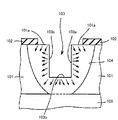
- a line having a predetermined depth from the surface of the N-type silicon substrate 101 is formed on a portion corresponding to the isolation region of the N-type silicon substrate 101, for example, on the scribe line SL by dicing or etching.
- the groove 103 is line-etched to reduce a margin for stress, and vibration during substrate transportation is formed.
- wafer cracks occur in the manufacturing process due to stress on the film.
- the groove processing is performed only in one direction only on the substrate surface, there is a limit to further reducing the diffusion time for forming the isolation region for element isolation, which is not suitable for a thick wafer.
Landscapes
- Element Separation (AREA)
- Thyristors (AREA)
- Dicing (AREA)
Abstract
Description
入した後に拡散して、N型シリコン基板101内に深くP型アイソレーション拡散層104を形成し、N型シリコン基板101の表層部にP型ベース拡散層105を形成し、N型シリコン基板101の裏面側にP型アノード拡散層106をそれぞれ形成する。
2 オリフラ
3 半導体チップ
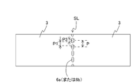
SL スクライブライン
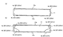
4a,4b 円形穴
5a,5b アイソレーション拡散層
6a,6b 長円形穴
7a,7b アイソレーション拡散層
11 半導体ウエハ(N型基板)
12a,12b 第1酸化絶縁膜
13a,13b 第2酸化絶縁膜
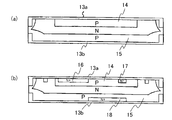
14 表面側のP型拡散層
15 裏面側のP型拡散層
16、17 表面側のN型拡散層
18 裏面側のN型拡散層
19 CVD膜
20 PIコート膜
図1は、本発明の実施形態1における半導体素子基板として半導体ウエハを概略的に示す平面図である。
上記実施形態1では、半導体ウエハの両面に形成された円形穴4a,4bの各ピッチが互いにずれていない場合について説明したが、本実施形態2では、半導体ウエハの両面に形成された円形穴4a,4bの各ピッチが互いに半ピッチだけ順次ずれている場合について説明する。
上記実施形態1、2では、半導体ウエハの両面に有底の円形穴4a,4bが形成された場合について説明したが、本実施形態3では、半導体ウエハの両面に、円形穴4a,4bの円形以外の穴形状として長円形穴や4角形穴(正方形または長方形)などがあるが、ここでは長円形穴が形成された場合について説明する。
上記実施形態1~3では、半導体素子基板およびその製造方法について説明したが、本実施形態4では、具体的にサイリスタ素子基板およびその製造方法について説明する。
Claims (5)
- 複数の半導体装置がマトリクス状に配置され、互いに隣接する半導体装置間のスクライブラインに沿って不連続に複数の穴が配設され、該複数の穴の周りにそれぞれ素子分離用のアイソレーション拡散層が形成されている半導体素子基板。
- 前記複数の穴は基板両面からそれぞれ前記スクライブラインに沿って形成されて前記素子分離用の一導電型の各アイソレーション拡散層が該基板両面から深さ方向中央部に達して隣接穴間および上下に互いに少なくとも一部が重なるように形成されている請求項1に記載の半導体素子基板。
- 前記基板表面から形成された複数の穴のピッチと前記基板裏面から形成された複数の穴のピッチとが互いにずれて形成されている請求項2に記載の半導体素子基板。
- 前記スクライブラインの方向に隣接する前記隣接穴間の繋がり部分の距離と、前記基板表面の穴の底面と前記基板裏面の穴の底面の間の深さ方向距離とが同一である請求項2または3に記載の半導体素子基板。
- 基板の片面または両面に、スクライブラインに沿った不連続な複数の穴を形成する穴形成工程と、該穴を介してウエハ両面から不純物をイオン注入して不純物領域を形成する不純物注入工程と、加熱処理により該不純物領域を拡散してアイソレーション拡散層を形成するアイソレーション拡散工程と、該アイソレーション拡散層で囲まれた素子分離領域毎に半導体装置を形成する半導体装置形成工程とを有する半導体素子基板の製造方法。
Priority Applications (3)
| Application Number | Priority Date | Filing Date | Title |
|---|---|---|---|
| JP2015530675A JP6111335B2 (ja) | 2013-08-08 | 2014-06-26 | 半導体素子基板およびその製造方法 |
| US14/906,006 US20160148875A1 (en) | 2013-08-08 | 2014-06-26 | Semiconductor element substrate, and method for producing same |
| CN201480044667.XA CN105453250A (zh) | 2013-08-08 | 2014-06-26 | 半导体元件衬底及其制造方法 |
Applications Claiming Priority (2)
| Application Number | Priority Date | Filing Date | Title |
|---|---|---|---|
| JP2013-165615 | 2013-08-08 | ||
| JP2013165615 | 2013-08-08 |
Publications (1)
| Publication Number | Publication Date |
|---|---|
| WO2015019540A1 true WO2015019540A1 (ja) | 2015-02-12 |
Family
ID=52460903
Family Applications (1)
| Application Number | Title | Priority Date | Filing Date |
|---|---|---|---|
| PCT/JP2014/003426 Ceased WO2015019540A1 (ja) | 2013-08-08 | 2014-06-26 | 半導体素子基板およびその製造方法 |
Country Status (4)
| Country | Link |
|---|---|
| US (1) | US20160148875A1 (ja) |
| JP (1) | JP6111335B2 (ja) |
| CN (1) | CN105453250A (ja) |
| WO (1) | WO2015019540A1 (ja) |
Cited By (2)
| Publication number | Priority date | Publication date | Assignee | Title |
|---|---|---|---|---|
| EP3142143A1 (en) * | 2015-09-11 | 2017-03-15 | ABB Technology AG | Method for manufacturing a power semiconductor device |
| US11398572B2 (en) | 2017-09-08 | 2022-07-26 | Hamamatsu Photonics K.K. | Semiconductor wafer manufacturing method, method of manufacturing semiconductor energy beam detecting element, and semiconductor wafer |
Families Citing this family (2)
| Publication number | Priority date | Publication date | Assignee | Title |
|---|---|---|---|---|
| JP7142606B2 (ja) * | 2019-06-04 | 2022-09-27 | 三菱電機株式会社 | 半導体装置 |
| CN115621122B (zh) * | 2021-07-14 | 2025-11-14 | 长鑫存储技术有限公司 | 半导体器件形成阵列圆形孔的制备方法 |
Citations (4)
| Publication number | Priority date | Publication date | Assignee | Title |
|---|---|---|---|---|
| JPH07235660A (ja) * | 1992-09-30 | 1995-09-05 | Rohm Co Ltd | サイリスタの製造方法 |
| JP2001185727A (ja) * | 1999-10-15 | 2001-07-06 | Fuji Electric Co Ltd | 半導体装置およびその製造方法 |
| JP2006164997A (ja) * | 2004-12-02 | 2006-06-22 | Toyota Motor Corp | 半導体装置の製造方法 |
| JP2012004174A (ja) * | 2010-06-14 | 2012-01-05 | Fuji Electric Co Ltd | 逆阻止型絶縁ゲート形バイポーラトランジスタおよびその製造方法 |
Family Cites Families (56)
| Publication number | Priority date | Publication date | Assignee | Title |
|---|---|---|---|---|
| US3365794A (en) * | 1964-05-15 | 1968-01-30 | Transitron Electronic Corp | Semiconducting device |
| US3458781A (en) * | 1966-07-18 | 1969-07-29 | Unitrode Corp | High-voltage planar semiconductor devices |
| US3535774A (en) * | 1968-07-09 | 1970-10-27 | Rca Corp | Method of fabricating semiconductor devices |
| US3612959A (en) * | 1969-01-31 | 1971-10-12 | Unitrode Corp | Planar zener diodes having uniform junction breakdown characteristics |
| US3628107A (en) * | 1969-05-05 | 1971-12-14 | Gen Electric | Passivated semiconductor device with peripheral protective junction |
| US3608186A (en) * | 1969-10-30 | 1971-09-28 | Jearld L Hutson | Semiconductor device manufacture with junction passivation |
| US3664894A (en) * | 1970-02-24 | 1972-05-23 | Rca Corp | Method of manufacturing semiconductor devices having high planar junction breakdown voltage |
| JPS4974486A (ja) * | 1972-11-17 | 1974-07-18 | ||
| US3972113A (en) * | 1973-05-14 | 1976-08-03 | Mitsubishi Denki Kabushiki Kaisha | Process of producing semiconductor devices |
| DE2340128C3 (de) * | 1973-08-08 | 1982-08-12 | SEMIKRON Gesellschaft für Gleichrichterbau u. Elektronik mbH, 8500 Nürnberg | Halbleiterbauelement hoher Sperrfähigkeit |
| US3896477A (en) * | 1973-11-07 | 1975-07-22 | Jearld L Hutson | Multilayer semiconductor switching devices |
| US4063272A (en) * | 1975-11-26 | 1977-12-13 | General Electric Company | Semiconductor device and method of manufacture thereof |
| JPS52101967A (en) * | 1976-02-23 | 1977-08-26 | Agency Of Ind Science & Technol | Semiconductor device |
| JPS584814B2 (ja) * | 1976-04-27 | 1983-01-27 | 三菱電機株式会社 | 半導体装置 |
| DE2633324C2 (de) * | 1976-07-24 | 1983-09-15 | SEMIKRON Gesellschaft für Gleichrichterbau u. Elektronik mbH, 8500 Nürnberg | Verfahren zum Herstellen von Halbleiterbauelementen hoher Sperrspannungsbelastbarkeit |
| US4040877A (en) * | 1976-08-24 | 1977-08-09 | Westinghouse Electric Corporation | Method of making a transistor device |
| DE2730130C2 (de) * | 1976-09-14 | 1987-11-12 | Mitsubishi Denki K.K., Tokyo | Verfahren zum Herstellen von Halbleiterbauelementen |
| DE2753207C2 (de) * | 1976-11-30 | 1989-10-12 | Mitsubishi Denki K.K., Tokio/Tokyo | Verfahren zum Herstellen von Halbleiterbauelementen |
| US4137100A (en) * | 1977-10-26 | 1979-01-30 | Western Electric Company | Forming isolation and device regions due to enhanced diffusion of impurities in semiconductor material by laser |
| DE2751485A1 (de) * | 1977-11-18 | 1979-05-23 | Semikron Gleichrichterbau | Verfahren zum herstellen von halbleiterkoerpern mit definiertem, durch aetzen erzielten und mit einem glas abgedeckten randprofil |
| US4249962A (en) * | 1979-09-11 | 1981-02-10 | Western Electric Company, Inc. | Method of removing contaminating impurities from device areas in a semiconductor wafer |
| US4325182A (en) * | 1980-08-25 | 1982-04-20 | General Electric Company | Fast isolation diffusion |
| US4570173A (en) * | 1981-05-26 | 1986-02-11 | General Electric Company | High-aspect-ratio hollow diffused regions in a semiconductor body |
| US4681656A (en) * | 1983-02-22 | 1987-07-21 | Byrum James E | IC carrier system |
| DE3324551A1 (de) * | 1983-07-07 | 1985-01-17 | Wacker-Chemitronic Gesellschaft für Elektronik-Grundstoffe mbH, 8263 Burghausen | Verfahren zur kennzeichnung von halbleiteroberflaechen durch laserstrahlung |
| JPS6222451A (ja) * | 1985-07-22 | 1987-01-30 | Sharp Corp | 半導体基板のpn接合アイソレ−シヨン方法 |
| EP0238694B1 (en) * | 1986-03-27 | 1992-01-29 | Ibm Deutschland Gmbh | Method of forming identically positioned alignment marks on opposite sides of a semiconductor wafer |
| US4814296A (en) * | 1987-08-28 | 1989-03-21 | Xerox Corporation | Method of fabricating image sensor dies for use in assembling arrays |
| US5213994A (en) * | 1989-05-30 | 1993-05-25 | Motorola, Inc. | Method of making high voltage semiconductor device |
| US5000811A (en) * | 1989-11-22 | 1991-03-19 | Xerox Corporation | Precision buttable subunits via dicing |
| JP3496347B2 (ja) * | 1995-07-13 | 2004-02-09 | 株式会社デンソー | 半導体装置及びその製造方法 |
| DE19601261C1 (de) * | 1996-01-16 | 1997-04-10 | Itt Ind Gmbh Deutsche | Verfahren und Hilfsvorrichtung zum Herstellen von Halbleiterschaltungselementen |
| US5872046A (en) * | 1996-04-10 | 1999-02-16 | Texas Instruments Incorporated | Method of cleaning wafer after partial saw |
| KR100273704B1 (ko) * | 1997-12-20 | 2000-12-15 | 윤종용 | 반도체기판제조방법 |
| US6339251B2 (en) * | 1998-11-10 | 2002-01-15 | Samsung Electronics Co., Ltd | Wafer grooves for reducing semiconductor wafer warping |
| WO2003028072A1 (en) * | 2001-09-20 | 2003-04-03 | Renesas Technology Corp. | Method for manufacturing semiconductor device |
| NL1019613C2 (nl) * | 2001-12-19 | 2003-06-20 | Micronit Microfluidics Bv | Werkwijze voor het verdelen van een substraat in een aantal individuele chipdelen. |
| KR100940530B1 (ko) * | 2003-01-17 | 2010-02-10 | 삼성전자주식회사 | 실리콘 광소자 제조방법 및 이에 의해 제조된 실리콘광소자 및 이를 적용한 화상 입력 및/또는 출력장치 |
| JP2003332270A (ja) * | 2002-05-15 | 2003-11-21 | Renesas Technology Corp | 半導体装置およびその製造方法 |
| CN1241253C (zh) * | 2002-06-24 | 2006-02-08 | 丰田合成株式会社 | 半导体元件的制造方法 |
| WO2004015764A2 (en) * | 2002-08-08 | 2004-02-19 | Leedy Glenn J | Vertical system integration |
| JP4579489B2 (ja) * | 2002-09-02 | 2010-11-10 | 新光電気工業株式会社 | 半導体チップ製造方法及び半導体チップ |
| WO2004105089A2 (en) * | 2003-05-15 | 2004-12-02 | Pan Jit Americas, Inc. | Low capacitance over-voltage protection thyristor device |
| JP4660224B2 (ja) * | 2004-03-30 | 2011-03-30 | 三洋電機株式会社 | 半導体レーザ装置 |
| JP4930322B2 (ja) * | 2006-11-10 | 2012-05-16 | ソニー株式会社 | 半導体発光素子、光ピックアップ装置および情報記録再生装置 |
| US8629532B2 (en) * | 2007-05-08 | 2014-01-14 | Taiwan Semiconductor Manufacturing Co., Ltd. | Semiconductor wafer with assisting dicing structure and dicing method thereof |
| US7888236B2 (en) * | 2007-05-14 | 2011-02-15 | Taiwan Semiconductor Manufacturing Co., Ltd. | Semiconductor device and fabrication methods thereof |
| WO2009139417A1 (ja) * | 2008-05-13 | 2009-11-19 | 富士電機デバイステクノロジー株式会社 | 半導体装置およびその製造方法 |
| US8064492B2 (en) * | 2009-01-26 | 2011-11-22 | Sanyo Electric Co., Ltd. | Method of manufacturing semiconductor laser device, semiconductor laser device and light apparatus |
| JP5560931B2 (ja) * | 2010-06-14 | 2014-07-30 | 富士電機株式会社 | 超接合半導体装置の製造方法 |
| US8361884B2 (en) * | 2010-06-22 | 2013-01-29 | Infineon Technologies Ag | Plasma dicing and semiconductor devices formed thereof |
| CN102244093B (zh) * | 2011-07-28 | 2013-09-25 | 江苏捷捷微电子股份有限公司 | 一种降低对通隔离扩散横向扩散宽度的结构及方法 |
| JP5803457B2 (ja) * | 2011-09-08 | 2015-11-04 | 三菱電機株式会社 | レーザダイオード素子の製造方法 |
| JP2013108111A (ja) * | 2011-11-18 | 2013-06-06 | Tokyo Electron Ltd | 基板の処理方法及びテンプレート |
| FR2987698B1 (fr) * | 2012-03-02 | 2014-04-04 | St Microelectronics Tours Sas | Composant de puissance vertical |
| JP6142496B2 (ja) * | 2012-10-12 | 2017-06-07 | 富士電機株式会社 | 半導体装置の製造方法 |
-
2014
- 2014-06-26 CN CN201480044667.XA patent/CN105453250A/zh active Pending
- 2014-06-26 US US14/906,006 patent/US20160148875A1/en not_active Abandoned
- 2014-06-26 JP JP2015530675A patent/JP6111335B2/ja not_active Expired - Fee Related
- 2014-06-26 WO PCT/JP2014/003426 patent/WO2015019540A1/ja not_active Ceased
Patent Citations (4)
| Publication number | Priority date | Publication date | Assignee | Title |
|---|---|---|---|---|
| JPH07235660A (ja) * | 1992-09-30 | 1995-09-05 | Rohm Co Ltd | サイリスタの製造方法 |
| JP2001185727A (ja) * | 1999-10-15 | 2001-07-06 | Fuji Electric Co Ltd | 半導体装置およびその製造方法 |
| JP2006164997A (ja) * | 2004-12-02 | 2006-06-22 | Toyota Motor Corp | 半導体装置の製造方法 |
| JP2012004174A (ja) * | 2010-06-14 | 2012-01-05 | Fuji Electric Co Ltd | 逆阻止型絶縁ゲート形バイポーラトランジスタおよびその製造方法 |
Cited By (2)
| Publication number | Priority date | Publication date | Assignee | Title |
|---|---|---|---|---|
| EP3142143A1 (en) * | 2015-09-11 | 2017-03-15 | ABB Technology AG | Method for manufacturing a power semiconductor device |
| US11398572B2 (en) | 2017-09-08 | 2022-07-26 | Hamamatsu Photonics K.K. | Semiconductor wafer manufacturing method, method of manufacturing semiconductor energy beam detecting element, and semiconductor wafer |
Also Published As
| Publication number | Publication date |
|---|---|
| JP6111335B2 (ja) | 2017-04-05 |
| JPWO2015019540A1 (ja) | 2017-03-02 |
| US20160148875A1 (en) | 2016-05-26 |
| CN105453250A (zh) | 2016-03-30 |
Similar Documents
| Publication | Publication Date | Title |
|---|---|---|
| CN101414553B (zh) | 半导体晶片的制造方法 | |
| CN107833921B (zh) | 开关器件和制造开关器件的方法 | |
| JP6111335B2 (ja) | 半導体素子基板およびその製造方法 | |
| CN105321824B (zh) | 半导体装置的制造方法 | |
| US20170047316A1 (en) | Semiconductor device | |
| CN104756233A (zh) | 半导体器件的制造方法 | |
| CN109872974A (zh) | 具有集成pn二极管温度传感器的半导体器件 | |
| WO2012137412A1 (ja) | 半導体装置およびその製造方法 | |
| KR102881646B1 (ko) | 반도체 소자 및 그의 제조 방법 | |
| JP2015230920A (ja) | 半導体装置 | |
| JP4873002B2 (ja) | 半導体装置の製造方法 | |
| JP6623824B2 (ja) | 半導体装置およびその製造方法 | |
| JP2016086002A (ja) | 半導体装置及びその製造方法 | |
| JP5073933B2 (ja) | 半導体装置及びその製造方法 | |
| JP5636751B2 (ja) | 逆阻止型絶縁ゲート形バイポーラトランジスタおよびその製造方法 | |
| CN102222619B (zh) | 半导体装置的制造方法 | |
| JP7009933B2 (ja) | 半導体装置 | |
| JP2022178412A (ja) | 半導体装置及び半導体装置の製造方法 | |
| JP2014086431A (ja) | 半導体装置及びその製造方法 | |
| WO2014203881A1 (ja) | 炭化珪素半導体素子の製造方法 | |
| JP5191109B2 (ja) | 接合型電界効果トランジスタ | |
| JP4260777B2 (ja) | 半導体装置及びその製造方法 | |
| JP2007180243A (ja) | 半導体装置及びその製造方法 | |
| CN100521244C (zh) | 结型场效应晶体管的制造方法 | |
| JP2018206870A (ja) | 半導体素子及びその製造方法 |
Legal Events
| Date | Code | Title | Description |
|---|---|---|---|
| WWE | Wipo information: entry into national phase |
Ref document number: 201480044667.X Country of ref document: CN |
|
| 121 | Ep: the epo has been informed by wipo that ep was designated in this application |
Ref document number: 14834387 Country of ref document: EP Kind code of ref document: A1 |
|
| ENP | Entry into the national phase |
Ref document number: 2015530675 Country of ref document: JP Kind code of ref document: A |
|
| WWE | Wipo information: entry into national phase |
Ref document number: 14906006 Country of ref document: US |
|
| NENP | Non-entry into the national phase |
Ref country code: DE |
|
| 122 | Ep: pct application non-entry in european phase |
Ref document number: 14834387 Country of ref document: EP Kind code of ref document: A1 |