WO2014188569A1 - ダイオード内蔵igbt - Google Patents
ダイオード内蔵igbt Download PDFInfo
- Publication number
- WO2014188569A1 WO2014188569A1 PCT/JP2013/064408 JP2013064408W WO2014188569A1 WO 2014188569 A1 WO2014188569 A1 WO 2014188569A1 JP 2013064408 W JP2013064408 W JP 2013064408W WO 2014188569 A1 WO2014188569 A1 WO 2014188569A1
- Authority
- WO
- WIPO (PCT)
- Prior art keywords
- region
- emitter
- schottky contact
- upper body
- igbt
- Prior art date
- Legal status (The legal status is an assumption and is not a legal conclusion. Google has not performed a legal analysis and makes no representation as to the accuracy of the status listed.)
- Ceased
Links
Images



Classifications
-
- H—ELECTRICITY
- H10—SEMICONDUCTOR DEVICES; ELECTRIC SOLID-STATE DEVICES NOT OTHERWISE PROVIDED FOR
- H10D—INORGANIC ELECTRIC SEMICONDUCTOR DEVICES
- H10D84/00—Integrated devices formed in or on semiconductor substrates that comprise only semiconducting layers, e.g. on Si wafers or on GaAs-on-Si wafers
- H10D84/40—Integrated devices formed in or on semiconductor substrates that comprise only semiconducting layers, e.g. on Si wafers or on GaAs-on-Si wafers characterised by the integration of at least one component covered by groups H10D12/00 or H10D30/00 with at least one component covered by groups H10D10/00 or H10D18/00, e.g. integration of IGFETs with BJTs
- H10D84/401—Combinations of FETs or IGBTs with BJTs
- H10D84/403—Combinations of FETs or IGBTs with BJTs and with one or more of diodes, resistors or capacitors
- H10D84/406—Combinations of FETs or IGBTs with vertical BJTs and with one or more of diodes, resistors or capacitors
-
- H—ELECTRICITY
- H10—SEMICONDUCTOR DEVICES; ELECTRIC SOLID-STATE DEVICES NOT OTHERWISE PROVIDED FOR
- H10D—INORGANIC ELECTRIC SEMICONDUCTOR DEVICES
- H10D12/00—Bipolar devices controlled by the field effect, e.g. insulated-gate bipolar transistors [IGBT]
- H10D12/411—Insulated-gate bipolar transistors [IGBT]
- H10D12/441—Vertical IGBTs
- H10D12/461—Vertical IGBTs having non-planar surfaces, e.g. having trenches, recesses or pillars in the surfaces of the emitter, base or collector regions
- H10D12/481—Vertical IGBTs having non-planar surfaces, e.g. having trenches, recesses or pillars in the surfaces of the emitter, base or collector regions having gate structures on slanted surfaces, on vertical surfaces, or in grooves, e.g. trench gate IGBTs
-
- H—ELECTRICITY
- H10—SEMICONDUCTOR DEVICES; ELECTRIC SOLID-STATE DEVICES NOT OTHERWISE PROVIDED FOR
- H10D—INORGANIC ELECTRIC SEMICONDUCTOR DEVICES
- H10D62/00—Semiconductor bodies, or regions thereof, of devices having potential barriers
- H10D62/10—Shapes, relative sizes or dispositions of the regions of the semiconductor bodies; Shapes of the semiconductor bodies
- H10D62/124—Shapes, relative sizes or dispositions of the regions of semiconductor bodies or of junctions between the regions
- H10D62/126—Top-view geometrical layouts of the regions or the junctions
- H10D62/127—Top-view geometrical layouts of the regions or the junctions of cellular field-effect devices, e.g. multicellular DMOS transistors or IGBTs
-
- H—ELECTRICITY
- H10—SEMICONDUCTOR DEVICES; ELECTRIC SOLID-STATE DEVICES NOT OTHERWISE PROVIDED FOR
- H10D—INORGANIC ELECTRIC SEMICONDUCTOR DEVICES
- H10D62/00—Semiconductor bodies, or regions thereof, of devices having potential barriers
- H10D62/10—Shapes, relative sizes or dispositions of the regions of the semiconductor bodies; Shapes of the semiconductor bodies
- H10D62/13—Semiconductor regions connected to electrodes carrying current to be rectified, amplified or switched, e.g. source or drain regions
- H10D62/141—Anode or cathode regions of thyristors; Collector or emitter regions of gated bipolar-mode devices, e.g. of IGBTs
- H10D62/142—Anode regions of thyristors or collector regions of gated bipolar-mode devices
-
- H—ELECTRICITY
- H10—SEMICONDUCTOR DEVICES; ELECTRIC SOLID-STATE DEVICES NOT OTHERWISE PROVIDED FOR
- H10D—INORGANIC ELECTRIC SEMICONDUCTOR DEVICES
- H10D62/00—Semiconductor bodies, or regions thereof, of devices having potential barriers
- H10D62/60—Impurity distributions or concentrations
-
- H—ELECTRICITY
- H10—SEMICONDUCTOR DEVICES; ELECTRIC SOLID-STATE DEVICES NOT OTHERWISE PROVIDED FOR
- H10D—INORGANIC ELECTRIC SEMICONDUCTOR DEVICES
- H10D64/00—Electrodes of devices having potential barriers
- H10D64/20—Electrodes characterised by their shapes, relative sizes or dispositions
- H10D64/27—Electrodes not carrying the current to be rectified, amplified, oscillated or switched, e.g. gates
- H10D64/311—Gate electrodes for field-effect devices
- H10D64/411—Gate electrodes for field-effect devices for FETs
- H10D64/511—Gate electrodes for field-effect devices for FETs for IGFETs
- H10D64/512—Disposition of the gate electrodes, e.g. buried gates
- H10D64/513—Disposition of the gate electrodes, e.g. buried gates within recesses in the substrate, e.g. trench gates, groove gates or buried gates
-
- H—ELECTRICITY
- H10—SEMICONDUCTOR DEVICES; ELECTRIC SOLID-STATE DEVICES NOT OTHERWISE PROVIDED FOR
- H10D—INORGANIC ELECTRIC SEMICONDUCTOR DEVICES
- H10D8/00—Diodes
- H10D8/60—Schottky-barrier diodes
-
- H—ELECTRICITY
- H10—SEMICONDUCTOR DEVICES; ELECTRIC SOLID-STATE DEVICES NOT OTHERWISE PROVIDED FOR
- H10D—INORGANIC ELECTRIC SEMICONDUCTOR DEVICES
- H10D84/00—Integrated devices formed in or on semiconductor substrates that comprise only semiconducting layers, e.g. on Si wafers or on GaAs-on-Si wafers
- H10D84/60—Integrated devices formed in or on semiconductor substrates that comprise only semiconducting layers, e.g. on Si wafers or on GaAs-on-Si wafers characterised by the integration of at least one component covered by groups H10D10/00 or H10D18/00, e.g. integration of BJTs
- H10D84/611—Combinations of BJTs and one or more of diodes, resistors or capacitors
- H10D84/613—Combinations of vertical BJTs and one or more of diodes, resistors or capacitors
- H10D84/617—Combinations of vertical BJTs and only diodes
-
- H—ELECTRICITY
- H10—SEMICONDUCTOR DEVICES; ELECTRIC SOLID-STATE DEVICES NOT OTHERWISE PROVIDED FOR
- H10D—INORGANIC ELECTRIC SEMICONDUCTOR DEVICES
- H10D84/00—Integrated devices formed in or on semiconductor substrates that comprise only semiconducting layers, e.g. on Si wafers or on GaAs-on-Si wafers
- H10D84/80—Integrated devices formed in or on semiconductor substrates that comprise only semiconducting layers, e.g. on Si wafers or on GaAs-on-Si wafers characterised by the integration of at least one component covered by groups H10D12/00 or H10D30/00, e.g. integration of IGFETs
- H10D84/811—Combinations of field-effect devices and one or more diodes, capacitors or resistors
Definitions
- This specification discloses a semiconductor device (referred to as a diode built-in IGBT) in which both an IGBT (Insulated Gate Bipolar Transistor) and a diode are formed on the same semiconductor substrate.
- a technique for preventing an increase in saturation current and a reduction in short-circuit withstand capability while lowering the on-voltage of the IGBT is disclosed.
- the IGBT has a structure in which a first conductivity type (for example, n-type) emitter region and a first conductivity type drift region are separated by a second conductivity type (for example, p-type) body region.
- a first conductivity type barrier layer is inserted into a second conductivity type body region, and the body region in contact with the emitter region and the body region in contact with the drift region are formed by the barrier layer. Separation techniques are also known. According to this technique, minority carriers can be prevented from escaping from the drift region to the emitter electrode, conductivity modulation can be activated, and the resistance when the IGBT is turned on can be lowered (the on-voltage is lowered).
- Patent Document 1 further discloses a technology for realizing a reverse conducting IGBT (RC (Reverse-Conducting) -IGBT) by forming an IGBT and a free wheeling diode on the same semiconductor substrate.
- RC Reverse-Conducting
- Patent Document 1 further discloses a technology for realizing a reverse conducting IGBT (RC (Reverse-Conducting) -IGBT) by forming an IGBT and a free wheeling diode on the same semiconductor substrate.
- RC Reverse-Conducting
- Japanese Patent Application No. 2012-166576 discloses a technique for forming a Schottky diode using a first conductive type semiconductor region that reaches the first conductive type barrier layer through the second conductive type body region from the surface of the semiconductor substrate. Disclosed in documents and drawings. However, the application has not yet been published at the time of filing this application.
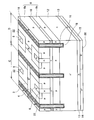
- FIG. 1 is a diagram schematically showing an example in which a technique for forming a Schottky diode using a region reaching a barrier layer from the surface of a semiconductor substrate (referred to as a Schottky contact region) is incorporated in an IGBT.
- Reference numeral 2 is the surface of the semiconductor substrate
- 4 is an emitter region
- 6 is a Schottky contact region
- 8 is a body region
- 10 is a barrier layer
- 12 is a drift region
- 14 is a collector region
- 16 is a gate electrode
- 18 is gate insulation.
- a film 20 is the back surface of the semiconductor substrate.
- the emitter region 4, the Schottky contact region 6, the barrier layer 10, and the drift region 12 are of the first conductivity type (for example, n-type), and the body region 8 and the collector region 14 are of the second conductivity type (for example, p-type).
- the body region 8 is separated by the barrier layer 10 into an upper body region 8 a in contact with the emitter region 4 and a lower body region 8 b in contact with the drain region 12.
- the Schottky contact region 6 reaches the barrier layer 10 from the surface 2 of the semiconductor substrate through the upper body region 8a.
- An emitter electrode (not shown) is formed on the surface 2 of the semiconductor substrate.
- the emitter electrode is in ohmic contact with the emitter region 4 and the upper body region 8 a, is in Schottky contact with the Schottky contact region 6, and is insulated from the gate electrode 16 by the gate insulating film 18.
- a collector electrode (not shown) is formed on the back surface 20 of the semiconductor substrate. The collector electrode is in ohmic contact with the collector region 14.
- the emitter electrode is an anode electrode of the Schottky diode, and the collector electrode is a cathode electrode of the Schottky diode.
- the emitter electrode is grounded and a positive voltage is applied to the collector electrode.
- This state corresponds to a state in which a reverse bias is applied to the Schottky diode.
- a positive voltage is applied to the gate electrode 16
- the body region 8 in a range facing the gate electrode 16 through the gate insulating film 18 is inverted to n-type, and the emitter region 4, the inverted upper body region 8a, the barrier layer 10,
- the inverted lower body region 8b and the drift region 12 are conducted, and electrons are injected from the emitter electrode into the drift region 12.
- the potential of the emitter electrode becomes higher than the potential of the collector electrode due to the inductive component of the load circuit connected to the IGBT.
- a forward bias is applied to the Schottky interface between the emitter electrode (the anode electrode of the diode) and the Schottky contact region 6, and a forward current flows through the Schottky diode.
- a Schottky diode operates as a freewheeling diode.
- a Schottky diode is formed by the emitter electrode and the Schottky contact region 6 and the like.
- the Schottky diode operates as a free wheel diode.
- the diode is incorporated in the IGBT. There is also.
- the diode built-in IGBT using the barrier layer 10 and the Schottky contact region 6 has characteristics of low resistance between the collector and the emitter when the IGBT is turned on and low leakage current, and has low loss. On the other hand, there remains a problem that the saturation current is high, and it is easily broken when a short circuit occurs in the load circuit or the like. In this specification, a technique for making it difficult to break down while using the barrier layer 10 and the Schottky contact region 6 is disclosed.
- An arrow A in FIG. 1 indicates a current path passing through the inversion layer formed when the IGBT is turned on.
- An arrow A is the only current path of an IGBT without a diode.
- an arrow B indicates a current path from the inversion layer formed in the lower body region 8b to the emitter region 4 via the barrier layer 10 and the Schottky contact region 6.
- the emitter region is actually measured from the Schottky contact region 6 via the upper body region 8a. 4 current flows.
- a reverse bias acts between the Schottky contact region 6 and the emitter electrode, and no current flows from the Schottky contact region 6 to the emitter electrode.
- the upper body region 8a is formed by injecting impurities from the surface 2 of the semiconductor substrate and then diffusing. At this time, since the impurities are implanted with energy that penetrates to a certain distance from the surface 2, the impurity concentration in the vicinity of the surface 2 is lower than the impurity concentration at the depth that penetrates from the surface to some extent.
- FIG. 2 shows the relationship between the emitter-collector voltage and current.
- a curve C1 shows the measurement result of the IGBT not provided with the diode
- a curve C2 shows the measurement result of the IGBT provided with the diode using the barrier layer 10 and the Schottky contact region 6.
- Saturation current of an IGBT diode is not installed together whereas a I A, the saturation current of the IGBT barrier layer 10 and the Schottky contact region 6 is provided in conjunction with increases in I A + I B.
- I A is the current due to the current path of arrow A
- I B was confirmed to be the current due to the current path of arrow B.
- VCC in FIG. 2 indicates a power supply voltage applied to the IGBT and the load circuit.
- the power supply voltage VCC is applied to the IGBT.
- the energy generated by the diode built IGBT during short-circuit was found to increase from V CC ⁇ I A to V CC ⁇ (I A + I B).
- the barrier layer 10 and the Schottky contact region 6 are provided side by side, the amount of heat generated per unit time increases, so the rate of temperature rise of the diode built-in IGBT increases, the time to reach the breakdown temperature decreases, and the short-circuit tolerance decreases. It has been found.
- This specification discloses a technique for improving the characteristics of a semiconductor device by using a barrier layer and a Schottky contact region, and at the same time making the diode built-in IGBT difficult to be destroyed.
- the total distance between the Schottky contact region and the emitter region is the sum of the distance of the depletion layer extending from the Schottky contact region into the upper body region and the distance of the depletion layer extending from the emitter region into the upper body region. Punch through when the distance is exceeded.
- the total distance is the potential difference between the Schottky contact region and the emitter region (when the IGBT is on, a reverse bias acts between the emitter electrode and the Schottky contact region.
- the potential is different from the potential of the emitter electrode (equal to the potential of the emitter region) and the amount of charge present in the upper body region. If the potential difference is large, the total distance is long, and if the charge amount is large, the total distance is short.
- the potential difference can be grasped by measurement or analysis.
- the occurrence of punch-through can be prevented by adjusting the charge amount to satisfy the relationship of “the total distance generated by the potential difference ⁇ the distance between the Schottky contact region and the emitter region”.
- monovalent ions are implanted to adjust the conductivity type of the upper body region. In this case, the charge amount is proportional to the impurity concentration.
- the impurity concentration in the vicinity of the surface of the upper body region in the conventional technique is low and does not satisfy the expression (2).
- the concentration is increased, it is possible to obtain a result of not punching through between the Schottky contact region and the emitter region.
- the concentration is increased, the current path indicated by the arrow B in FIG. 1 is not formed, the problem of increasing the saturation current does not occur, the temperature increase rate at the time of short-circuit does not increase, and the short-circuit tolerance is increased. The result that it does not fall can be obtained.
- the short-circuit withstand capability decreases even if the barrier layer and the Schottky contact region are formed. There is nothing.
- a region that prevents punch-through from occurring may be formed between the Schottky contact region and the emitter region.
- an insulating region extending in the depth direction from the surface may be formed on the surface of the upper body region located between the Schottky contact region and the emitter region.
- a combination of a trench gate electrode and a gate insulating film may be used.
- a region having a higher concentration than the upper body region may be formed near the surface of the upper body region.
- the gap between the depletion layer extending from the Schottky contact region to the upper body region and the depletion layer extending from the emitter region to the upper body region is blocked to prevent the occurrence of punch-through.
- Any blocking region may be formed so as to cross a portion where punch-through occurs, and does not need to cover the entire thickness of the upper body region, and completely surrounds the Schottky contact region or the emitter region. It is not necessary to be out.
- barrier layer Utilizing the barrier layer, minority carriers can be prevented from falling from the drift region to the emitter electrode, and conductivity modulation can be activated.
- a Schottky diode structure using an emitter electrode (to be a Schottky electrode), a Schottky contact region, and a barrier layer can be formed.
- the IGBT When the IGBT is turned on, a current path from the barrier layer to the emitter region via the Schottky contact region and the upper body region can be prevented from being formed, and an increase in saturation current can be suppressed. It is possible to prevent a short circuit withstand capability from being lowered.
- the figure which planarly viewed IGBT with a built-in diode of FIG. The figure which planarly viewed IGBT with built-in diode of 3rd Example.
- the semiconductor structure of the first embodiment is the same as that shown in FIG. A duplicate description of the matters already described is omitted. As shown in FIG. 1, a region having a composition different from that of the upper body region 8 a is not formed in the upper body region 8 a in a range separating the Schottky contact region 6 and the emitter region 4.
- the semiconductor structure of the first embodiment is the same as that shown in FIG. In the IGBT with built-in diode of the first embodiment, the impurity concentration of the upper body region 8a in the vicinity of the surface 2 of the semiconductor substrate is increased, and the Schottky contact region 6 and the emitter region 4 are prohibited from punching through. . This prevents a short circuit withstand capability from being lowered.
- a blocking region that prevents the depletion layer from reaching the collector region 14 may be provided between the drift region 12 and the collector region 14. This blocking area will be described in the second embodiment.
- N is an impurity concentration in the vicinity of the surface of the upper body region 8a.
- the impurity is assumed to be monovalent. In that case, if the impurity concentration N satisfies the following equation, punch-through between the Schottky contact region 6 and the emitter region 4 will not occur.
- N > 2 ⁇ ⁇ s ⁇ (Vbi ⁇ V) / (q ⁇ L 2 ) (2)
- ⁇ s is the dielectric constant of the semiconductor
- Vbi the built-in potential
- q is the elementary charge amount.
- the impurity concentration N of the upper body region 8a in the vicinity of the surface 2 of the semiconductor substrate satisfies the formula (2), and the Schottky contact region 6 and the emitter region 4 punch through. Is prohibited. This prevents the short circuit withstand capability from being lowered.
- the gate-on voltage of the IGBT is Vg and the threshold voltage of the IGBT is Vth, the potential of the Schottky contact region 6 and the barrier layer 10 does not exceed Vg ⁇ Vth.
- the high concentration region 22 is formed in a range surrounding the Schottky contact region 6.
- the high concentration region 22 is formed in the vicinity of the surface of the upper body region 8 a and in a range separating the Schottky contact region 6 and the emitter region 4.
- the high concentration region 22 can satisfy the expression (2). Therefore, the impurity concentration of upper body region 8a can be adjusted freely.
- the impurity concentration of the body region 8 can be lowered to lower the threshold voltage of the IGBT. Further, when the high concentration region 22 is formed, even if the shortest distance between the Schottky contact region 6 and the emitter region 4 is shortened to L, punch-through can be prevented, so that the element can be miniaturized.
- a blocking region 13 that prevents the depletion layer from reaching the collector region 14 is formed between the drift region 12 and the collector region 14.
- the blocking region 13 is formed by a region into which n-type impurities are implanted at a high concentration.
- the emitter region 4 is not formed, and an n-type cathode region 15 is formed instead of the p-type collector region 14.
- the high concentration region 22 is not required.
- the high concentration region 22 may be formed.
- the high concentration region 22 is in ohmic contact with the emitter electrode, and the potential of the body region 8 is made equal to the potential of the emitter electrode.
- the high concentration region 22 becomes a body contact region that prevents the emitter region 4 and the Schottky contact region 6 from punching through and stabilizes the potential of the body region 8.
- the high concentration region 22 a only needs to be formed in a range that separates the Schottky contact region 6 and the emitter region 4 in the vicinity of the surface 2 of the semiconductor substrate, and is separated from the Schottky contact region 6. It may be formed in a range.
- the Schottky contact region 6 and the high-concentration region 22a are of the opposite conductivity type, and if they are separated from each other, it is possible to prevent the impurity implantation ranges from overlapping due to manufacturing tolerances. It is easy to optimize the impurity concentration of the high concentration region 22a. Alternatively, the size of the Schottky contact region 6 is prevented from fluctuating due to the manufacture of the high concentration region 22a.
- the gate electrode 16 and the gate insulating film 18 may extend in a lattice pattern.
- the high concentration region 22b having the shape shown in FIG. 6 can be used.
- the Schottky contact region 6 and the emitter region 4 can be separated by using the high concentration region 22c and the gate insulating film 18 in combination. Since both the high concentration region 22c and the gate insulating film 18 can stop the extension of the depletion layer, the combined use of the high concentration region 22c and the gate insulating film 18 indicates that the Schottky contact region 6 and the emitter region 4 punch through. Can be prevented.
- an insulating film that covers the wall surface of the trench may be used instead of the high concentration regions 22, 22 a, 22 b, and 22 c illustrated in FIGS. 3 to 7.
- an insulating film that covers the wall surface of the trench may be used instead of the high concentration regions 22, 22 a, 22 b, and 22 c illustrated in FIGS. 3 to 7.
- punch-through of the Schottky contact region 6 and the emitter region 4 can be prevented.
- a thin insulating layer is sufficient, and the element can be downsized.
- the trench may be filled with an insulator, or the trench wall may be covered with an insulating film, and the inside may be filled with a conductor. In the latter case, the Schottky contact region 6 and the emitter region 4 are separated by the gate insulating film.
Landscapes
- Metal-Oxide And Bipolar Metal-Oxide Semiconductor Integrated Circuits (AREA)
- Electrodes Of Semiconductors (AREA)
Abstract
Description
図2のVCCは、IGBTと負荷回路に印加される電源電圧を示している。負荷回路が短絡すれば、IGBTに電源電圧VCCが印加される。負荷回路の短絡時には、半導体装置に、単位時間当たり飽和電流×電源電圧(W=J/sec)のエネルギーが発生し、ダイオード内蔵IGBTが発熱する。バリア層10とショットキー接触領域6を併設すると、短絡時にダイオード内蔵IGBTで発生するエネルギーが、VCC×IAからVCC×(IA+IB)に増加することが分かった。バリア層10とショットキー接触領域6を併設すると、単位時間あたりの発熱量が増大するために、ダイオード内蔵IGBTの昇温速度が大きくなり、破壊温度に達する時間が短くなり、短絡耐量が低下することが判明した。
ショットキー接触領域から上部ボディ領域内に伸びる空乏層の距離と、エミッタ領域から上部ボディ領域内に伸びる空乏層の距離を合計した距離(合計距離)が、ショットキー接触領域とエミッタ領域の間の距離以上となるとパンチスルーする。その合計距離は、ショットキー接触領域とエミッタ領域の間の電位差(IGBTがオンしている状態では、エミッタ電極とショットキー接触領域の間に逆方向バイアスが作用するために、ショットキー接触領域の電位はエミッタ電極の電位(エミッタ領域の電位に等しい)とは異なっている)と、上部ボディ領域に存在している電荷量による。電位差が大きければ合計距離は長く、電荷量が大きければ合計距離は短い。電位差は、計測ないし解析することで把握することができる。「その電位差で生じる合計距離<ショットキー接触領域とエミッタ領域の間の距離」の関係となる電荷量に調整しておけば、パンチスルーの発生を防止することができる。通常は、1価のイオンを注入して上部ボディ領域の導電型を調整する。その場合電荷量は不純物濃度に比例する。
W2=2・Εs・(Vbi―V)/(q・N)・・・・(1)
上記において、Εsは半導体の誘電率、Vbiは内蔵電位、qは素電荷量である。
ショットキー接触領域とエミッタ領域の間の距離をLとすると、(1)式から、
N>2・Εs・(Vbi―V)/(q・L2)・・・・(2)
の場合に、W<Lとなり、ショットキー接触領域とエミッタ領域の間がパンチスルーしない結果を得ることができることがわかる。(2)式において、誘電率Εsと、素電荷量qは既知であり、内蔵電位Vbiと、ショットキー接触領域とエミッタ領域の間の距離Lと、ショットキー接触領域とエミッタ領域の間の電圧差Vは、測定することができる。したがって、(2)式から、ショットキー接触領域とエミッタ領域の間がパンチスルーしないために必要な不純物濃度を決定することができる。
上部ボディ領域の少なくとも表面近傍における不純物濃度を、ショットキー接触領域とエミッタ領域の間がパンチスルーしない濃度にまで上昇させると、バリア層とショットキー接触領域を形成しても、短絡耐量が低下することがない。
ショットキー接触領域とエミッタ領域の間にパンチスルーの発生を防止する領域を形成してもよい。例えば、ショットキー接触領域とエミッタ領域の間に位置する上部ボディ領域の表面に、表面から深さ方向に伸びる絶縁領域を形成してもよい。絶縁領域に代えて、トレンチゲート電極とゲート絶縁膜の組み合わせを用いてもよい。あるいは、上部ボディ領域の表面近傍に、上部ボディ領域よりも高濃度の領域を形成してもよい。いずれであっても、ショットキー接触領域から上部ボディ領域に伸びる空乏層とエミッタ領域から上部ボディ領域に伸びる空乏層の間を遮断し、パンチスルーの発生を防止する。いずれの遮断領域であっても、パンチスルーが発生する個所を横断するように形成すればよく、上部ボディ領域の全厚みに亘っている必要はないし、ショットキー接触領域ないしエミッタ領域を完全に取り囲んでいる必要はない。
(1)バリア層を利用して少数キャリアがドリフト領域からエミッタ電極に抜けることを抑制でき、電導度変調を活発化させられる。
(2)エミッタ電極(ショットキー電極となる)とショットキー接触領域とバリア層を利用するショットキーダイオード構造を形成することができる。
(3)IGBTの導通時に、バリア層からショットキー接触領域と上部ボディ領域を経由してエミッタ領域に達する電流経路が形成されないようにすることができ、飽和電流の増大を抑制できる。短絡耐量の低下を防止できる。
(第1実施例の特徴)ショットキー接触領域とエミッタ領域を分離する上部ボディ領域の中に上部ボディ領域とは異なる組成の領域が形成されていない。ショットキー接触領域とエミッタ領域を分離する範囲における上部ボディ領域の不純物濃度は一様である。
(第2実施例の特徴)p型の上部ボディ領域の中に、それよりも高濃度のp型領域が形成されている。その高濃度p型領域は、半導体基板を平面視したときに、ショットキー接触領域を取り囲んでいる。
(第5実施例の特徴)トレンチの内部に形成されている絶縁体と前記高濃度p型領域が複合してショットキー接触領域を取り囲んでいる。
(第1実施例)
第1実施例の半導体構造は図1に示したものと同じである。すでに説明した事項の重複説明は省略する。図1に示すように、ショットキー接触領域6とエミッタ領域4を分離する範囲の上部ボディ領域8aの中に、上部ボディ領域8aとは異なる組成の領域は形成されていない。第1実施例の半導体構造は図1に示したものと同じである。第1実施例のダイオード内蔵IGBTでは、半導体基板の表面2の近傍における上部ボディ領域8aの不純物濃度が濃くされており、ショットキー接触領域6とエミッタ領域4がパンチスルーすることを禁止している。これによって短絡耐量の低下を防止している。ドリフト領域12とコレクタ領域14の間に、空乏層がコレクタ領域14に達することを防止する遮断領域を設けてもよい。この遮断領域については、第2実施例で説明する。
N>2・Εs・(Vbi―V)/(q・L2)・・・・(2)
上記において、Εsは半導体の誘電率、Vbiは内蔵電位、qは素電荷量である。
第1実施例のダイオード内蔵IGBTでは、半導体基板の表面2の近傍における上部ボディ領域8aの不純物濃度Nが(2)式を満たしており、ショットキー接触領域6とエミッタ領域4がパンチスルーすることを禁止している。これによって短絡耐量の低下を防いでいる。
IGBTのゲートオン電圧をVgとし、IGBTの閾値電圧をVthとしたとき、ショットキー接触領域6とバリア層10の電位は、Vg-Vthを超えることがない。Vg=15Vであり、Vth=6Vである場合、Vg-Vth=9Vとなり、(2)式から、パンチスルーの発生を防止するのに必要な電荷量(L・N)は1.2E12cm-2であることがわかる。これから、不純物濃度Nと距離Lを決定することができる。
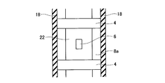
図3と図4を参照して第2実施例を説明する。以下では図1と異なる点のみを説明し、重複説明を省略する。第2実施例のダイオード内蔵IGBTでは、ダイオードとIGBTの両者が作り込まれている範囲Cと、ダイオードのみが作られている範囲Dが交互に設けられている。
範囲Cでは、エミッタ領域4とショットキー接触領域6の双方が形成されている。第2実施例では、ゲート電極16の長手方向において、エミッタ領域4とショットキー接触領域6が異なる位置に形成されている。p型の上部ボディ領域8aの表面近傍に、それよりもp型不純物の濃度が濃い高濃度領域22が形成されている。半導体基板の表面2を平面視したときに、高濃度領域22はショットキー接触領域6を取り囲む範囲に形成されている。高濃度領域22は、上部ボディ領域8aの表面近傍であって、ショットキー接触領域6とエミッタ領域4を分離する範囲に形成されている。高濃度領域22を形成すると、高濃度領域22によって前記(2)式を満たすことができる。そのために、上部ボディ領域8aの不純物濃度を自由に調整することができる。ボディ領域8の不純物濃度を下げてIGBTの閾値電圧を下げるといったことができる。また、高濃度領域22を形成すると、ショットキー接触領域6とエミッタ領域4の間の最短距離をLと短くしてもパンチスルーしないようにできることから、素子の小型化が可能となる。
またダイオードだけが形成されている範囲Dでは、エミッタ領域4が形成されていないし、p型のコレクタ領域14に代えてn型のカソード領域15が形成されている。範囲Dでは、エミッタ領域が存在しないことから、高濃度領域22は必要とされない。必要ではないが、範囲Cと同様に、高濃度領域22を形成してもよい。
高濃度領域22はエミッタ電極とオーミック接触し、ボディ領域8の電位をエミッタ電極の電位に等しくする。ボディ領域8の電位が安定すると、IGBTの挙動が安定する。高濃度領域22は、エミッタ領域4とショットキー接触領域6がパンチスルーすることを防止し、ボディ領域8の電位を安定させるボディコンタクト領域となる。
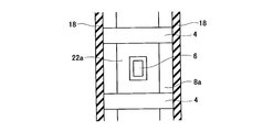
図5に示すように、高濃度領域22aは、半導体基板の表面2の近傍においてショットキー接触領域6とエミッタ領域4を分離する範囲に形成されていればよく、ショットキー接触領域6から離れた範囲に形成されていてもよい。ショットキー接触領域6と高濃度領域22aは反対導電型であり、両者を離しておくと、製造時の公差によって不純物の注入範囲がオーバラップすることを防止でき、ショットキー接触領域6の不純物濃度と高濃度領域22aの不純物濃度の夫々を最適化しやすい。あるいは、高濃度領域22aの製造によってショットキー接触領域6のサイズが変動することを防止する。
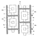
図6に示すように、半導体基板の表面2において、ゲート電極16とゲート絶縁膜18が格子状に伸びている場合がある。その場合は、図6に示す形状の高濃度領域22bを用いることができる。
図7に示すように、高濃度領域22cとゲート絶縁膜18を併用することによってショットキー接触領域6とエミッタ領域4を分離することもできる。高濃度領域22cもゲート絶縁膜18も空乏層の伸長を止めることができることから、高濃度領域22cとゲート絶縁膜18を併用することによってショットキー接触領域6とエミッタ領域4がパンチスルーすることを防止できる。
図示はしないが、図3から図7に例示した高濃度領域22,22a、22b、22cに代えて、トレンチの壁面を覆う絶縁膜を利用してもよい。その場合も、ショットキー接触領域6とエミッタ領域4がパンチスルーすることを防止できる。絶縁膜でパンチスルーの発生を防止する場合には、薄い絶縁層で足りことから、素子の小型化が可能となる。
第6実施例のトレンチを利用する場合、トレンチの中に絶縁体を充填してもよいし、トレンチの壁面を絶縁膜で覆い、その内側に導体を充填してもよい。後者の場合、ゲート絶縁膜によって、ショットキー接触領域6とエミッタ領域4を分離することになる。
4:エミッタ領域
6:ショットキー接触領域
8:ボディ領域
8a:上部ボディ領域
8b:下部ボディ領域
10:バリア層
12:ドレイン領域
13:遮断領域
14:コレクタ領域
15:カソード領域
16:ゲート電極
18:ゲート絶縁膜
20:半導体基板の裏面
22,22a,22b,22c:高濃度領域
Claims (2)
- 半導体基板内にエミッタ領域と上部ボディ領域とバリア層と下部ボディ領域とドリフト領域とコレクタ領域が順に配置されており、半導体基板の表面からエミッタ領域と上部ボディ領域とバリア層と下部ボディ領域を貫通してドリフト領域に達するトレンチが形成されており、そのトレンチの壁面が絶縁膜で覆われており、壁面が絶縁膜で覆われているトレンチの内部にゲート電極が配置されており、半導体基板の表面にエミッタ領域と導通するエミッタ電極が形成されており、半導体基板の裏面にコレクタ領域と導通するコレクタ電極が形成されているIGBT構造と、
上部ボディ領域を貫通してバリア層に到達しているとともにエミッタ電極にショットキー接触しているショットキー接触領域を備えているショットキーダイオード構造とを合わせ持っているダイオード内蔵IGBTであり、
半導体基板の表面においてショットキー接触領域とエミッタ領域が上部ボディ領域によって分離されており、その分離部の不純物濃度が「分離部に形成される空乏層の距離<ショットキー接触領域とエミッタ領域の分離距離」の関係を満たす濃度に設定されているダイオード内蔵IGBT。 - 半導体基板内にエミッタ領域と上部ボディ領域とバリア層と下部ボディ領域とドリフト領域とコレクタ領域が順に配置されており、半導体基板の表面からエミッタ領域と上部ボディ領域とバリア層と下部ボディ領域を貫通してドリフト領域に達するトレンチが形成されており、そのトレンチの壁面が絶縁膜で覆われており、壁面が絶縁膜で覆われているトレンチの内部にゲート電極が配置されており、半導体基板の表面にエミッタ領域と導通するエミッタ電極が形成されており、半導体基板の裏面にコレクタ領域と導通するコレクタ電極が形成されているIGBT構造と、
上部ボディ領域を貫通してバリア層に到達しているとともにエミッタ電極にショットキー接触しているショットキー接触領域を備えているショットキーダイオード構造とを合わせ持っているダイオード内蔵IGBTであり、
半導体基板の表面においてショットキー接触領域とエミッタ領域が上部ボディ領域によって分離されており、その分離部に、ショットキー接触領域から分離部に伸びる空乏層とエミッタ領域から分離部に伸びる空乏層を遮断する遮断領域が形成されているダイオード内蔵IGBT。
Priority Applications (5)
| Application Number | Priority Date | Filing Date | Title |
|---|---|---|---|
| US14/888,291 US9412737B2 (en) | 2013-05-23 | 2013-05-23 | IGBT with a built-in-diode |
| PCT/JP2013/064408 WO2014188569A1 (ja) | 2013-05-23 | 2013-05-23 | ダイオード内蔵igbt |
| CN201380076833.XA CN105378931A (zh) | 2013-05-23 | 2013-05-23 | 内置有二极管的igbt |
| JP2015518006A JPWO2014188569A1 (ja) | 2013-05-23 | 2013-05-23 | ダイオード内蔵igbt |
| DE112013007102.9T DE112013007102T5 (de) | 2013-05-23 | 2013-05-23 | IGBT mit eingebauter Diode |
Applications Claiming Priority (1)
| Application Number | Priority Date | Filing Date | Title |
|---|---|---|---|
| PCT/JP2013/064408 WO2014188569A1 (ja) | 2013-05-23 | 2013-05-23 | ダイオード内蔵igbt |
Publications (1)
| Publication Number | Publication Date |
|---|---|
| WO2014188569A1 true WO2014188569A1 (ja) | 2014-11-27 |
Family
ID=51933151
Family Applications (1)
| Application Number | Title | Priority Date | Filing Date |
|---|---|---|---|
| PCT/JP2013/064408 Ceased WO2014188569A1 (ja) | 2013-05-23 | 2013-05-23 | ダイオード内蔵igbt |
Country Status (5)
| Country | Link |
|---|---|
| US (1) | US9412737B2 (ja) |
| JP (1) | JPWO2014188569A1 (ja) |
| CN (1) | CN105378931A (ja) |
| DE (1) | DE112013007102T5 (ja) |
| WO (1) | WO2014188569A1 (ja) |
Cited By (6)
| Publication number | Priority date | Publication date | Assignee | Title |
|---|---|---|---|---|
| JP2016225345A (ja) * | 2015-05-27 | 2016-12-28 | トヨタ自動車株式会社 | 逆導通igbt |
| JP2017107948A (ja) * | 2015-12-08 | 2017-06-15 | トヨタ自動車株式会社 | Igbt |
| CN113394279A (zh) * | 2020-03-11 | 2021-09-14 | 三菱电机株式会社 | 半导体装置 |
| JP2021158199A (ja) * | 2020-03-26 | 2021-10-07 | 三菱電機株式会社 | 半導体装置 |
| WO2025134384A1 (ja) * | 2023-12-22 | 2025-06-26 | サンケン電気株式会社 | 半導体装置及び電子機器 |
| US12575390B2 (en) | 2019-08-13 | 2026-03-10 | Fuji Electric Co., Ltd. | Semiconductor device and manufacturing method thereof |
Families Citing this family (12)
| Publication number | Priority date | Publication date | Assignee | Title |
|---|---|---|---|---|
| JP6003961B2 (ja) * | 2014-11-04 | 2016-10-05 | トヨタ自動車株式会社 | 半導体装置 |
| JP2016096307A (ja) * | 2014-11-17 | 2016-05-26 | トヨタ自動車株式会社 | 半導体装置 |
| JP6063915B2 (ja) | 2014-12-12 | 2017-01-18 | 株式会社豊田中央研究所 | 逆導通igbt |
| JP6589817B2 (ja) * | 2016-10-26 | 2019-10-16 | 株式会社デンソー | 半導体装置 |
| JP6610508B2 (ja) * | 2016-11-09 | 2019-11-27 | 株式会社デンソー | 半導体装置 |
| JP7029711B2 (ja) * | 2017-11-29 | 2022-03-04 | 国立研究開発法人産業技術総合研究所 | 半導体装置 |
| US11764209B2 (en) * | 2020-10-19 | 2023-09-19 | MW RF Semiconductors, LLC | Power semiconductor device with forced carrier extraction and method of manufacture |
| JP7528743B2 (ja) * | 2020-11-27 | 2024-08-06 | 三菱電機株式会社 | 半導体装置 |
| JP7701610B2 (ja) * | 2021-09-02 | 2025-07-02 | ミネベアパワーデバイス株式会社 | 半導体装置、半導体装置の製造方法、電力変換装置 |
| CN115985941B (zh) * | 2023-03-21 | 2023-06-23 | 上海埃积半导体有限公司 | 一种纵向rc-igbt结构及其制备方法 |
| JP2025020741A (ja) * | 2023-07-31 | 2025-02-13 | ミネベアパワーデバイス株式会社 | 半導体装置 |
| DE102024205993A1 (de) | 2024-06-27 | 2025-12-31 | Robert Bosch Gesellschaft mit beschränkter Haftung | Halbleiterbauelement mit einem ersten Bereich und einem zweiten Bereich |
Citations (3)
| Publication number | Priority date | Publication date | Assignee | Title |
|---|---|---|---|---|
| JP2010010401A (ja) * | 2008-06-27 | 2010-01-14 | Hitachi Ltd | 横型igbtとそれを用いたモータ制御装置 |
| JP2013048230A (ja) * | 2011-07-27 | 2013-03-07 | Toyota Central R&D Labs Inc | ダイオード、半導体装置およびmosfet |
| JP2013051345A (ja) * | 2011-08-31 | 2013-03-14 | Toyota Central R&D Labs Inc | ダイオード、半導体装置およびmosfet |
Family Cites Families (8)
| Publication number | Priority date | Publication date | Assignee | Title |
|---|---|---|---|---|
| US6998678B2 (en) * | 2001-05-17 | 2006-02-14 | Infineon Technologies Ag | Semiconductor arrangement with a MOS-transistor and a parallel Schottky-diode |
| US7157785B2 (en) * | 2003-08-29 | 2007-01-02 | Fuji Electric Device Technology Co., Ltd. | Semiconductor device, the method of manufacturing the same, and two-way switching device using the semiconductor devices |
| CN102804359B (zh) * | 2009-06-11 | 2014-06-04 | 丰田自动车株式会社 | 半导体装置 |
| DE102010039258B4 (de) * | 2010-08-12 | 2018-03-15 | Infineon Technologies Austria Ag | Transistorbauelement mit reduziertem Kurzschlussstrom |
| JP5636808B2 (ja) | 2010-08-17 | 2014-12-10 | 株式会社デンソー | 半導体装置 |
| US8716746B2 (en) | 2010-08-17 | 2014-05-06 | Denso Corporation | Semiconductor device |
| US20120217541A1 (en) * | 2011-02-24 | 2012-08-30 | Force Mos Technology Co., Ltd. | Igbt with integrated mosfet and fast switching diode |
| JP5706275B2 (ja) * | 2011-08-31 | 2015-04-22 | 株式会社豊田中央研究所 | ダイオード、半導体装置およびmosfet |
-
2013
- 2013-05-23 JP JP2015518006A patent/JPWO2014188569A1/ja active Pending
- 2013-05-23 US US14/888,291 patent/US9412737B2/en not_active Expired - Fee Related
- 2013-05-23 DE DE112013007102.9T patent/DE112013007102T5/de not_active Withdrawn
- 2013-05-23 CN CN201380076833.XA patent/CN105378931A/zh active Pending
- 2013-05-23 WO PCT/JP2013/064408 patent/WO2014188569A1/ja not_active Ceased
Patent Citations (3)
| Publication number | Priority date | Publication date | Assignee | Title |
|---|---|---|---|---|
| JP2010010401A (ja) * | 2008-06-27 | 2010-01-14 | Hitachi Ltd | 横型igbtとそれを用いたモータ制御装置 |
| JP2013048230A (ja) * | 2011-07-27 | 2013-03-07 | Toyota Central R&D Labs Inc | ダイオード、半導体装置およびmosfet |
| JP2013051345A (ja) * | 2011-08-31 | 2013-03-14 | Toyota Central R&D Labs Inc | ダイオード、半導体装置およびmosfet |
Cited By (9)
| Publication number | Priority date | Publication date | Assignee | Title |
|---|---|---|---|---|
| JP2016225345A (ja) * | 2015-05-27 | 2016-12-28 | トヨタ自動車株式会社 | 逆導通igbt |
| JP2017107948A (ja) * | 2015-12-08 | 2017-06-15 | トヨタ自動車株式会社 | Igbt |
| US12575390B2 (en) | 2019-08-13 | 2026-03-10 | Fuji Electric Co., Ltd. | Semiconductor device and manufacturing method thereof |
| CN113394279A (zh) * | 2020-03-11 | 2021-09-14 | 三菱电机株式会社 | 半导体装置 |
| CN113394279B (zh) * | 2020-03-11 | 2024-08-27 | 三菱电机株式会社 | 半导体装置 |
| JP2021158199A (ja) * | 2020-03-26 | 2021-10-07 | 三菱電機株式会社 | 半導体装置 |
| JP7359053B2 (ja) | 2020-03-26 | 2023-10-11 | 三菱電機株式会社 | 半導体装置 |
| US11908954B2 (en) | 2020-03-26 | 2024-02-20 | Mitsubishi Electric Corporation | Semiconductor device with insulated gate bipolar transistor region and diode region provided on semiconductor substrate and adjacent to each other |
| WO2025134384A1 (ja) * | 2023-12-22 | 2025-06-26 | サンケン電気株式会社 | 半導体装置及び電子機器 |
Also Published As
| Publication number | Publication date |
|---|---|
| CN105378931A (zh) | 2016-03-02 |
| US9412737B2 (en) | 2016-08-09 |
| US20160071841A1 (en) | 2016-03-10 |
| DE112013007102T5 (de) | 2016-03-03 |
| JPWO2014188569A1 (ja) | 2017-02-23 |
Similar Documents
| Publication | Publication Date | Title |
|---|---|---|
| WO2014188569A1 (ja) | ダイオード内蔵igbt | |
| US9362393B2 (en) | Vertical semiconductor device including element active portion and voltage withstanding structure portion, and method of manufacturing the vertical semiconductor device | |
| KR101840967B1 (ko) | 반도체 장치 | |
| JP5612256B2 (ja) | 半導体装置 | |
| US9082815B2 (en) | Semiconductor device having carrier extraction in electric field alleviating layer | |
| JP5922886B2 (ja) | ダイオードおよび半導体装置 | |
| JP6606007B2 (ja) | スイッチング素子 | |
| JP5480084B2 (ja) | 半導体装置 | |
| US20160079369A1 (en) | Semiconductor device | |
| TW201611275A (zh) | 半導體裝置 | |
| JP6720818B2 (ja) | 半導体装置 | |
| JP5537359B2 (ja) | 半導体装置 | |
| JPWO2015029116A1 (ja) | 半導体装置 | |
| JP2017191817A (ja) | スイッチング素子の製造方法 | |
| JP6852541B2 (ja) | 半導体装置 | |
| JP6077309B2 (ja) | ダイオード及びダイオードを内蔵した半導体装置 | |
| JP6299658B2 (ja) | 絶縁ゲート型スイッチング素子 | |
| JP2014060299A (ja) | 半導体装置 | |
| JP2015195307A (ja) | 半導体装置 | |
| KR20140067445A (ko) | 전력 반도체 소자 | |
| US9356100B2 (en) | Semiconductor device | |
| JP6067957B2 (ja) | 半導体装置 | |
| US20190305127A1 (en) | Semiconductor device | |
| JP2012049428A5 (ja) | ||
| TW201535725A (zh) | 半導體裝置 |
Legal Events
| Date | Code | Title | Description |
|---|---|---|---|
| 121 | Ep: the epo has been informed by wipo that ep was designated in this application |
Ref document number: 13885063 Country of ref document: EP Kind code of ref document: A1 |
|
| ENP | Entry into the national phase |
Ref document number: 2015518006 Country of ref document: JP Kind code of ref document: A |
|
| WWE | Wipo information: entry into national phase |
Ref document number: 14888291 Country of ref document: US |
|
| WWE | Wipo information: entry into national phase |
Ref document number: 112013007102 Country of ref document: DE |
|
| 122 | Ep: pct application non-entry in european phase |
Ref document number: 13885063 Country of ref document: EP Kind code of ref document: A1 |