WO2014046052A1 - チップ支持基板、チップ支持方法、三次元集積回路、アセンブリ装置及び三次元集積回路の製造方法 - Google Patents
チップ支持基板、チップ支持方法、三次元集積回路、アセンブリ装置及び三次元集積回路の製造方法 Download PDFInfo
- Publication number
- WO2014046052A1 WO2014046052A1 PCT/JP2013/074876 JP2013074876W WO2014046052A1 WO 2014046052 A1 WO2014046052 A1 WO 2014046052A1 JP 2013074876 W JP2013074876 W JP 2013074876W WO 2014046052 A1 WO2014046052 A1 WO 2014046052A1
- Authority
- WO
- WIPO (PCT)
- Prior art keywords
- chip
- substrate
- support substrate
- region
- electrode
- Prior art date
- Legal status (The legal status is an assumption and is not a legal conclusion. Google has not performed a legal analysis and makes no representation as to the accuracy of the status listed.)
- Ceased
Links
Images










Classifications
-
- B—PERFORMING OPERATIONS; TRANSPORTING
- B23—MACHINE TOOLS; METAL-WORKING NOT OTHERWISE PROVIDED FOR
- B23K—SOLDERING OR UNSOLDERING; WELDING; CLADDING OR PLATING BY SOLDERING OR WELDING; CUTTING BY APPLYING HEAT LOCALLY, e.g. FLAME CUTTING; WORKING BY LASER BEAM
- B23K20/00—Non-electric welding by applying impact or other pressure, with or without the application of heat, e.g. cladding or plating
- B23K20/002—Non-electric welding by applying impact or other pressure, with or without the application of heat, e.g. cladding or plating specially adapted for particular articles or work
-
- B—PERFORMING OPERATIONS; TRANSPORTING
- B23—MACHINE TOOLS; METAL-WORKING NOT OTHERWISE PROVIDED FOR
- B23K—SOLDERING OR UNSOLDERING; WELDING; CLADDING OR PLATING BY SOLDERING OR WELDING; CUTTING BY APPLYING HEAT LOCALLY, e.g. FLAME CUTTING; WORKING BY LASER BEAM
- B23K20/00—Non-electric welding by applying impact or other pressure, with or without the application of heat, e.g. cladding or plating
- B23K20/02—Non-electric welding by applying impact or other pressure, with or without the application of heat, e.g. cladding or plating by means of a press ; Diffusion bonding
- B23K20/023—Thermo-compression bonding
-
- B—PERFORMING OPERATIONS; TRANSPORTING
- B23—MACHINE TOOLS; METAL-WORKING NOT OTHERWISE PROVIDED FOR
- B23K—SOLDERING OR UNSOLDERING; WELDING; CLADDING OR PLATING BY SOLDERING OR WELDING; CUTTING BY APPLYING HEAT LOCALLY, e.g. FLAME CUTTING; WORKING BY LASER BEAM
- B23K20/00—Non-electric welding by applying impact or other pressure, with or without the application of heat, e.g. cladding or plating
- B23K20/16—Non-electric welding by applying impact or other pressure, with or without the application of heat, e.g. cladding or plating with interposition of special material to facilitate connection of the parts, e.g. material for absorbing or producing gas
-
- H—ELECTRICITY
- H10—SEMICONDUCTOR DEVICES; ELECTRIC SOLID-STATE DEVICES NOT OTHERWISE PROVIDED FOR
- H10P—GENERIC PROCESSES OR APPARATUS FOR THE MANUFACTURE OR TREATMENT OF DEVICES COVERED BY CLASS H10
- H10P72/00—Handling or holding of wafers, substrates or devices during manufacture or treatment thereof
- H10P72/70—Handling or holding of wafers, substrates or devices during manufacture or treatment thereof for supporting or gripping
- H10P72/74—Handling or holding of wafers, substrates or devices during manufacture or treatment thereof for supporting or gripping using temporarily an auxiliary support
-
- H—ELECTRICITY
- H10—SEMICONDUCTOR DEVICES; ELECTRIC SOLID-STATE DEVICES NOT OTHERWISE PROVIDED FOR
- H10W—GENERIC PACKAGES, INTERCONNECTIONS, CONNECTORS OR OTHER CONSTRUCTIONAL DETAILS OF DEVICES COVERED BY CLASS H10
- H10W46/00—Marks applied to devices, e.g. for alignment or identification
-
- H—ELECTRICITY
- H10—SEMICONDUCTOR DEVICES; ELECTRIC SOLID-STATE DEVICES NOT OTHERWISE PROVIDED FOR
- H10W—GENERIC PACKAGES, INTERCONNECTIONS, CONNECTORS OR OTHER CONSTRUCTIONAL DETAILS OF DEVICES COVERED BY CLASS H10
- H10W70/00—Package substrates; Interposers; Redistribution layers [RDL]
- H10W70/60—Insulating or insulated package substrates; Interposers; Redistribution layers
- H10W70/62—Insulating or insulated package substrates; Interposers; Redistribution layers characterised by their interconnections
- H10W70/65—Shapes or dispositions of interconnections
-
- H—ELECTRICITY
- H10—SEMICONDUCTOR DEVICES; ELECTRIC SOLID-STATE DEVICES NOT OTHERWISE PROVIDED FOR
- H10W—GENERIC PACKAGES, INTERCONNECTIONS, CONNECTORS OR OTHER CONSTRUCTIONAL DETAILS OF DEVICES COVERED BY CLASS H10
- H10W72/00—Interconnections or connectors in packages
- H10W72/01—Manufacture or treatment
- H10W72/012—Manufacture or treatment of bump connectors, dummy bumps or thermal bumps
-
- H—ELECTRICITY
- H10—SEMICONDUCTOR DEVICES; ELECTRIC SOLID-STATE DEVICES NOT OTHERWISE PROVIDED FOR
- H10W—GENERIC PACKAGES, INTERCONNECTIONS, CONNECTORS OR OTHER CONSTRUCTIONAL DETAILS OF DEVICES COVERED BY CLASS H10
- H10W72/00—Interconnections or connectors in packages
- H10W72/01—Manufacture or treatment
- H10W72/013—Manufacture or treatment of die-attach connectors
-
- H—ELECTRICITY
- H10—SEMICONDUCTOR DEVICES; ELECTRIC SOLID-STATE DEVICES NOT OTHERWISE PROVIDED FOR
- H10W—GENERIC PACKAGES, INTERCONNECTIONS, CONNECTORS OR OTHER CONSTRUCTIONAL DETAILS OF DEVICES COVERED BY CLASS H10
- H10W72/00—Interconnections or connectors in packages
- H10W72/01—Manufacture or treatment
- H10W72/0198—Manufacture or treatment batch processes
-
- H—ELECTRICITY
- H10—SEMICONDUCTOR DEVICES; ELECTRIC SOLID-STATE DEVICES NOT OTHERWISE PROVIDED FOR
- H10W—GENERIC PACKAGES, INTERCONNECTIONS, CONNECTORS OR OTHER CONSTRUCTIONAL DETAILS OF DEVICES COVERED BY CLASS H10
- H10W72/00—Interconnections or connectors in packages
- H10W72/071—Connecting or disconnecting
- H10W72/0711—Apparatus therefor
-
- H—ELECTRICITY
- H10—SEMICONDUCTOR DEVICES; ELECTRIC SOLID-STATE DEVICES NOT OTHERWISE PROVIDED FOR
- H10W—GENERIC PACKAGES, INTERCONNECTIONS, CONNECTORS OR OTHER CONSTRUCTIONAL DETAILS OF DEVICES COVERED BY CLASS H10
- H10W72/00—Interconnections or connectors in packages
- H10W72/071—Connecting or disconnecting
- H10W72/072—Connecting or disconnecting of bump connectors
-
- H—ELECTRICITY
- H10—SEMICONDUCTOR DEVICES; ELECTRIC SOLID-STATE DEVICES NOT OTHERWISE PROVIDED FOR
- H10W—GENERIC PACKAGES, INTERCONNECTIONS, CONNECTORS OR OTHER CONSTRUCTIONAL DETAILS OF DEVICES COVERED BY CLASS H10
- H10W72/00—Interconnections or connectors in packages
- H10W72/071—Connecting or disconnecting
- H10W72/073—Connecting or disconnecting of die-attach connectors
-
- H—ELECTRICITY
- H10—SEMICONDUCTOR DEVICES; ELECTRIC SOLID-STATE DEVICES NOT OTHERWISE PROVIDED FOR
- H10W—GENERIC PACKAGES, INTERCONNECTIONS, CONNECTORS OR OTHER CONSTRUCTIONAL DETAILS OF DEVICES COVERED BY CLASS H10
- H10W72/00—Interconnections or connectors in packages
- H10W72/20—Bump connectors, e.g. solder bumps or copper pillars; Dummy bumps; Thermal bumps
-
- H—ELECTRICITY
- H10—SEMICONDUCTOR DEVICES; ELECTRIC SOLID-STATE DEVICES NOT OTHERWISE PROVIDED FOR
- H10W—GENERIC PACKAGES, INTERCONNECTIONS, CONNECTORS OR OTHER CONSTRUCTIONAL DETAILS OF DEVICES COVERED BY CLASS H10
- H10W72/00—Interconnections or connectors in packages
- H10W72/30—Die-attach connectors
-
- H—ELECTRICITY
- H10—SEMICONDUCTOR DEVICES; ELECTRIC SOLID-STATE DEVICES NOT OTHERWISE PROVIDED FOR
- H10W—GENERIC PACKAGES, INTERCONNECTIONS, CONNECTORS OR OTHER CONSTRUCTIONAL DETAILS OF DEVICES COVERED BY CLASS H10
- H10W78/00—Detachable holders for supporting packaged chips in operation
-
- H—ELECTRICITY
- H10—SEMICONDUCTOR DEVICES; ELECTRIC SOLID-STATE DEVICES NOT OTHERWISE PROVIDED FOR
- H10W—GENERIC PACKAGES, INTERCONNECTIONS, CONNECTORS OR OTHER CONSTRUCTIONAL DETAILS OF DEVICES COVERED BY CLASS H10
- H10W90/00—Package configurations
-
- H—ELECTRICITY
- H10—SEMICONDUCTOR DEVICES; ELECTRIC SOLID-STATE DEVICES NOT OTHERWISE PROVIDED FOR
- H10P—GENERIC PROCESSES OR APPARATUS FOR THE MANUFACTURE OR TREATMENT OF DEVICES COVERED BY CLASS H10
- H10P72/00—Handling or holding of wafers, substrates or devices during manufacture or treatment thereof
- H10P72/70—Handling or holding of wafers, substrates or devices during manufacture or treatment thereof for supporting or gripping
- H10P72/74—Handling or holding of wafers, substrates or devices during manufacture or treatment thereof for supporting or gripping using temporarily an auxiliary support
- H10P72/7416—Handling or holding of wafers, substrates or devices during manufacture or treatment thereof for supporting or gripping using temporarily an auxiliary support used during dicing or grinding
-
- H—ELECTRICITY
- H10—SEMICONDUCTOR DEVICES; ELECTRIC SOLID-STATE DEVICES NOT OTHERWISE PROVIDED FOR
- H10P—GENERIC PROCESSES OR APPARATUS FOR THE MANUFACTURE OR TREATMENT OF DEVICES COVERED BY CLASS H10
- H10P72/00—Handling or holding of wafers, substrates or devices during manufacture or treatment thereof
- H10P72/70—Handling or holding of wafers, substrates or devices during manufacture or treatment thereof for supporting or gripping
- H10P72/74—Handling or holding of wafers, substrates or devices during manufacture or treatment thereof for supporting or gripping using temporarily an auxiliary support
- H10P72/7434—Handling or holding of wafers, substrates or devices during manufacture or treatment thereof for supporting or gripping using temporarily an auxiliary support used in a transfer process involving at least two transfer steps, i.e. including an intermediate handle substrate
-
- H—ELECTRICITY
- H10—SEMICONDUCTOR DEVICES; ELECTRIC SOLID-STATE DEVICES NOT OTHERWISE PROVIDED FOR
- H10P—GENERIC PROCESSES OR APPARATUS FOR THE MANUFACTURE OR TREATMENT OF DEVICES COVERED BY CLASS H10
- H10P72/00—Handling or holding of wafers, substrates or devices during manufacture or treatment thereof
- H10P72/70—Handling or holding of wafers, substrates or devices during manufacture or treatment thereof for supporting or gripping
- H10P72/74—Handling or holding of wafers, substrates or devices during manufacture or treatment thereof for supporting or gripping using temporarily an auxiliary support
- H10P72/744—Details of chemical or physical process used for separating the auxiliary support from a device or a wafer
-
- H—ELECTRICITY
- H10—SEMICONDUCTOR DEVICES; ELECTRIC SOLID-STATE DEVICES NOT OTHERWISE PROVIDED FOR
- H10W—GENERIC PACKAGES, INTERCONNECTIONS, CONNECTORS OR OTHER CONSTRUCTIONAL DETAILS OF DEVICES COVERED BY CLASS H10
- H10W20/00—Interconnections in chips, wafers or substrates
- H10W20/01—Manufacture or treatment
- H10W20/021—Manufacture or treatment of interconnections within wafers or substrates
- H10W20/023—Manufacture or treatment of interconnections within wafers or substrates the interconnections being through-semiconductor vias
-
- H—ELECTRICITY
- H10—SEMICONDUCTOR DEVICES; ELECTRIC SOLID-STATE DEVICES NOT OTHERWISE PROVIDED FOR
- H10W—GENERIC PACKAGES, INTERCONNECTIONS, CONNECTORS OR OTHER CONSTRUCTIONAL DETAILS OF DEVICES COVERED BY CLASS H10
- H10W46/00—Marks applied to devices, e.g. for alignment or identification
- H10W46/101—Marks applied to devices, e.g. for alignment or identification characterised by the type of information, e.g. logos or symbols
-
- H—ELECTRICITY
- H10—SEMICONDUCTOR DEVICES; ELECTRIC SOLID-STATE DEVICES NOT OTHERWISE PROVIDED FOR
- H10W—GENERIC PACKAGES, INTERCONNECTIONS, CONNECTORS OR OTHER CONSTRUCTIONAL DETAILS OF DEVICES COVERED BY CLASS H10
- H10W46/00—Marks applied to devices, e.g. for alignment or identification
- H10W46/301—Marks applied to devices, e.g. for alignment or identification for alignment
-
- H—ELECTRICITY
- H10—SEMICONDUCTOR DEVICES; ELECTRIC SOLID-STATE DEVICES NOT OTHERWISE PROVIDED FOR
- H10W—GENERIC PACKAGES, INTERCONNECTIONS, CONNECTORS OR OTHER CONSTRUCTIONAL DETAILS OF DEVICES COVERED BY CLASS H10
- H10W70/00—Package substrates; Interposers; Redistribution layers [RDL]
- H10W70/60—Insulating or insulated package substrates; Interposers; Redistribution layers
- H10W70/62—Insulating or insulated package substrates; Interposers; Redistribution layers characterised by their interconnections
- H10W70/63—Vias, e.g. via plugs
- H10W70/635—Through-vias
-
- H—ELECTRICITY
- H10—SEMICONDUCTOR DEVICES; ELECTRIC SOLID-STATE DEVICES NOT OTHERWISE PROVIDED FOR
- H10W—GENERIC PACKAGES, INTERCONNECTIONS, CONNECTORS OR OTHER CONSTRUCTIONAL DETAILS OF DEVICES COVERED BY CLASS H10
- H10W70/00—Package substrates; Interposers; Redistribution layers [RDL]
- H10W70/60—Insulating or insulated package substrates; Interposers; Redistribution layers
- H10W70/67—Insulating or insulated package substrates; Interposers; Redistribution layers characterised by their insulating layers or insulating parts
- H10W70/69—Insulating materials thereof
- H10W70/698—Semiconductor materials that are electrically insulating, e.g. undoped silicon
-
- H—ELECTRICITY
- H10—SEMICONDUCTOR DEVICES; ELECTRIC SOLID-STATE DEVICES NOT OTHERWISE PROVIDED FOR
- H10W—GENERIC PACKAGES, INTERCONNECTIONS, CONNECTORS OR OTHER CONSTRUCTIONAL DETAILS OF DEVICES COVERED BY CLASS H10
- H10W72/00—Interconnections or connectors in packages
-
- H—ELECTRICITY
- H10—SEMICONDUCTOR DEVICES; ELECTRIC SOLID-STATE DEVICES NOT OTHERWISE PROVIDED FOR
- H10W—GENERIC PACKAGES, INTERCONNECTIONS, CONNECTORS OR OTHER CONSTRUCTIONAL DETAILS OF DEVICES COVERED BY CLASS H10
- H10W72/00—Interconnections or connectors in packages
- H10W72/01—Manufacture or treatment
- H10W72/012—Manufacture or treatment of bump connectors, dummy bumps or thermal bumps
- H10W72/01231—Manufacture or treatment of bump connectors, dummy bumps or thermal bumps using blanket deposition
- H10W72/01233—Manufacture or treatment of bump connectors, dummy bumps or thermal bumps using blanket deposition in liquid form, e.g. spin coating, spray coating or immersion coating
- H10W72/01235—Manufacture or treatment of bump connectors, dummy bumps or thermal bumps using blanket deposition in liquid form, e.g. spin coating, spray coating or immersion coating by plating, e.g. electroless plating or electroplating
-
- H—ELECTRICITY
- H10—SEMICONDUCTOR DEVICES; ELECTRIC SOLID-STATE DEVICES NOT OTHERWISE PROVIDED FOR
- H10W—GENERIC PACKAGES, INTERCONNECTIONS, CONNECTORS OR OTHER CONSTRUCTIONAL DETAILS OF DEVICES COVERED BY CLASS H10
- H10W72/00—Interconnections or connectors in packages
- H10W72/01—Manufacture or treatment
- H10W72/012—Manufacture or treatment of bump connectors, dummy bumps or thermal bumps
- H10W72/01231—Manufacture or treatment of bump connectors, dummy bumps or thermal bumps using blanket deposition
- H10W72/01238—Manufacture or treatment of bump connectors, dummy bumps or thermal bumps using blanket deposition in gaseous form, e.g. by CVD or PVD
-
- H—ELECTRICITY
- H10—SEMICONDUCTOR DEVICES; ELECTRIC SOLID-STATE DEVICES NOT OTHERWISE PROVIDED FOR
- H10W—GENERIC PACKAGES, INTERCONNECTIONS, CONNECTORS OR OTHER CONSTRUCTIONAL DETAILS OF DEVICES COVERED BY CLASS H10
- H10W72/00—Interconnections or connectors in packages
- H10W72/01—Manufacture or treatment
- H10W72/013—Manufacture or treatment of die-attach connectors
- H10W72/01331—Manufacture or treatment of die-attach connectors using blanket deposition
- H10W72/01336—Manufacture or treatment of die-attach connectors using blanket deposition in solid form, e.g. by using a powder or by laminating a foil
-
- H—ELECTRICITY
- H10—SEMICONDUCTOR DEVICES; ELECTRIC SOLID-STATE DEVICES NOT OTHERWISE PROVIDED FOR
- H10W—GENERIC PACKAGES, INTERCONNECTIONS, CONNECTORS OR OTHER CONSTRUCTIONAL DETAILS OF DEVICES COVERED BY CLASS H10
- H10W72/00—Interconnections or connectors in packages
- H10W72/071—Connecting or disconnecting
- H10W72/0711—Apparatus therefor
- H10W72/07141—Means for applying energy, e.g. ovens or lasers
-
- H—ELECTRICITY
- H10—SEMICONDUCTOR DEVICES; ELECTRIC SOLID-STATE DEVICES NOT OTHERWISE PROVIDED FOR
- H10W—GENERIC PACKAGES, INTERCONNECTIONS, CONNECTORS OR OTHER CONSTRUCTIONAL DETAILS OF DEVICES COVERED BY CLASS H10
- H10W72/00—Interconnections or connectors in packages
- H10W72/071—Connecting or disconnecting
- H10W72/0711—Apparatus therefor
- H10W72/07168—Means for storing or moving the material for the connector
-
- H—ELECTRICITY
- H10—SEMICONDUCTOR DEVICES; ELECTRIC SOLID-STATE DEVICES NOT OTHERWISE PROVIDED FOR
- H10W—GENERIC PACKAGES, INTERCONNECTIONS, CONNECTORS OR OTHER CONSTRUCTIONAL DETAILS OF DEVICES COVERED BY CLASS H10
- H10W72/00—Interconnections or connectors in packages
- H10W72/071—Connecting or disconnecting
- H10W72/0711—Apparatus therefor
- H10W72/07178—Means for aligning
-
- H—ELECTRICITY
- H10—SEMICONDUCTOR DEVICES; ELECTRIC SOLID-STATE DEVICES NOT OTHERWISE PROVIDED FOR
- H10W—GENERIC PACKAGES, INTERCONNECTIONS, CONNECTORS OR OTHER CONSTRUCTIONAL DETAILS OF DEVICES COVERED BY CLASS H10
- H10W72/00—Interconnections or connectors in packages
- H10W72/071—Connecting or disconnecting
- H10W72/0711—Apparatus therefor
- H10W72/07183—Means for monitoring
-
- H—ELECTRICITY
- H10—SEMICONDUCTOR DEVICES; ELECTRIC SOLID-STATE DEVICES NOT OTHERWISE PROVIDED FOR
- H10W—GENERIC PACKAGES, INTERCONNECTIONS, CONNECTORS OR OTHER CONSTRUCTIONAL DETAILS OF DEVICES COVERED BY CLASS H10
- H10W72/00—Interconnections or connectors in packages
- H10W72/071—Connecting or disconnecting
- H10W72/072—Connecting or disconnecting of bump connectors
- H10W72/07202—Connecting or disconnecting of bump connectors using auxiliary members
- H10W72/07204—Connecting or disconnecting of bump connectors using auxiliary members using temporary auxiliary members, e.g. sacrificial coatings
-
- H—ELECTRICITY
- H10—SEMICONDUCTOR DEVICES; ELECTRIC SOLID-STATE DEVICES NOT OTHERWISE PROVIDED FOR
- H10W—GENERIC PACKAGES, INTERCONNECTIONS, CONNECTORS OR OTHER CONSTRUCTIONAL DETAILS OF DEVICES COVERED BY CLASS H10
- H10W72/00—Interconnections or connectors in packages
- H10W72/071—Connecting or disconnecting
- H10W72/072—Connecting or disconnecting of bump connectors
- H10W72/07221—Aligning
- H10W72/07223—Active alignment, e.g. using optical alignment using marks or sensors
-
- H—ELECTRICITY
- H10—SEMICONDUCTOR DEVICES; ELECTRIC SOLID-STATE DEVICES NOT OTHERWISE PROVIDED FOR
- H10W—GENERIC PACKAGES, INTERCONNECTIONS, CONNECTORS OR OTHER CONSTRUCTIONAL DETAILS OF DEVICES COVERED BY CLASS H10
- H10W72/00—Interconnections or connectors in packages
- H10W72/071—Connecting or disconnecting
- H10W72/072—Connecting or disconnecting of bump connectors
- H10W72/07231—Techniques
- H10W72/07232—Compression bonding, e.g. thermocompression bonding
-
- H—ELECTRICITY
- H10—SEMICONDUCTOR DEVICES; ELECTRIC SOLID-STATE DEVICES NOT OTHERWISE PROVIDED FOR
- H10W—GENERIC PACKAGES, INTERCONNECTIONS, CONNECTORS OR OTHER CONSTRUCTIONAL DETAILS OF DEVICES COVERED BY CLASS H10
- H10W72/00—Interconnections or connectors in packages
- H10W72/071—Connecting or disconnecting
- H10W72/073—Connecting or disconnecting of die-attach connectors
- H10W72/07331—Connecting techniques
- H10W72/07337—Connecting techniques using a polymer adhesive, e.g. an adhesive based on silicone or epoxy
-
- H—ELECTRICITY
- H10—SEMICONDUCTOR DEVICES; ELECTRIC SOLID-STATE DEVICES NOT OTHERWISE PROVIDED FOR
- H10W—GENERIC PACKAGES, INTERCONNECTIONS, CONNECTORS OR OTHER CONSTRUCTIONAL DETAILS OF DEVICES COVERED BY CLASS H10
- H10W72/00—Interconnections or connectors in packages
- H10W72/20—Bump connectors, e.g. solder bumps or copper pillars; Dummy bumps; Thermal bumps
- H10W72/241—Dispositions, e.g. layouts
- H10W72/242—Dispositions, e.g. layouts relative to the surface, e.g. recessed, protruding
-
- H—ELECTRICITY
- H10—SEMICONDUCTOR DEVICES; ELECTRIC SOLID-STATE DEVICES NOT OTHERWISE PROVIDED FOR
- H10W—GENERIC PACKAGES, INTERCONNECTIONS, CONNECTORS OR OTHER CONSTRUCTIONAL DETAILS OF DEVICES COVERED BY CLASS H10
- H10W72/00—Interconnections or connectors in packages
- H10W72/20—Bump connectors, e.g. solder bumps or copper pillars; Dummy bumps; Thermal bumps
- H10W72/241—Dispositions, e.g. layouts
- H10W72/244—Dispositions, e.g. layouts relative to underlying supporting features, e.g. bond pads, RDLs or vias
-
- H—ELECTRICITY
- H10—SEMICONDUCTOR DEVICES; ELECTRIC SOLID-STATE DEVICES NOT OTHERWISE PROVIDED FOR
- H10W—GENERIC PACKAGES, INTERCONNECTIONS, CONNECTORS OR OTHER CONSTRUCTIONAL DETAILS OF DEVICES COVERED BY CLASS H10
- H10W72/00—Interconnections or connectors in packages
- H10W72/20—Bump connectors, e.g. solder bumps or copper pillars; Dummy bumps; Thermal bumps
- H10W72/251—Materials
- H10W72/252—Materials comprising solid metals or solid metalloids, e.g. PbSn, Ag or Cu
-
- H—ELECTRICITY
- H10—SEMICONDUCTOR DEVICES; ELECTRIC SOLID-STATE DEVICES NOT OTHERWISE PROVIDED FOR
- H10W—GENERIC PACKAGES, INTERCONNECTIONS, CONNECTORS OR OTHER CONSTRUCTIONAL DETAILS OF DEVICES COVERED BY CLASS H10
- H10W72/00—Interconnections or connectors in packages
- H10W72/20—Bump connectors, e.g. solder bumps or copper pillars; Dummy bumps; Thermal bumps
- H10W72/261—Functions other than electrical connecting
-
- H—ELECTRICITY
- H10—SEMICONDUCTOR DEVICES; ELECTRIC SOLID-STATE DEVICES NOT OTHERWISE PROVIDED FOR
- H10W—GENERIC PACKAGES, INTERCONNECTIONS, CONNECTORS OR OTHER CONSTRUCTIONAL DETAILS OF DEVICES COVERED BY CLASS H10
- H10W74/00—Encapsulations, e.g. protective coatings
- H10W74/01—Manufacture or treatment
- H10W74/014—Manufacture or treatment using batch processing
-
- H—ELECTRICITY
- H10—SEMICONDUCTOR DEVICES; ELECTRIC SOLID-STATE DEVICES NOT OTHERWISE PROVIDED FOR
- H10W—GENERIC PACKAGES, INTERCONNECTIONS, CONNECTORS OR OTHER CONSTRUCTIONAL DETAILS OF DEVICES COVERED BY CLASS H10
- H10W74/00—Encapsulations, e.g. protective coatings
- H10W74/01—Manufacture or treatment
- H10W74/019—Manufacture or treatment using temporary auxiliary substrates
-
- H—ELECTRICITY
- H10—SEMICONDUCTOR DEVICES; ELECTRIC SOLID-STATE DEVICES NOT OTHERWISE PROVIDED FOR
- H10W—GENERIC PACKAGES, INTERCONNECTIONS, CONNECTORS OR OTHER CONSTRUCTIONAL DETAILS OF DEVICES COVERED BY CLASS H10
- H10W74/00—Encapsulations, e.g. protective coatings
- H10W74/10—Encapsulations, e.g. protective coatings characterised by their shape or disposition
- H10W74/111—Encapsulations, e.g. protective coatings characterised by their shape or disposition the semiconductor body being completely enclosed
- H10W74/114—Encapsulations, e.g. protective coatings characterised by their shape or disposition the semiconductor body being completely enclosed by a substrate and the encapsulations
-
- H—ELECTRICITY
- H10—SEMICONDUCTOR DEVICES; ELECTRIC SOLID-STATE DEVICES NOT OTHERWISE PROVIDED FOR
- H10W—GENERIC PACKAGES, INTERCONNECTIONS, CONNECTORS OR OTHER CONSTRUCTIONAL DETAILS OF DEVICES COVERED BY CLASS H10
- H10W74/00—Encapsulations, e.g. protective coatings
- H10W74/10—Encapsulations, e.g. protective coatings characterised by their shape or disposition
- H10W74/15—Encapsulations, e.g. protective coatings characterised by their shape or disposition on active surfaces of flip-chip devices, e.g. underfills
-
- H—ELECTRICITY
- H10—SEMICONDUCTOR DEVICES; ELECTRIC SOLID-STATE DEVICES NOT OTHERWISE PROVIDED FOR
- H10W—GENERIC PACKAGES, INTERCONNECTIONS, CONNECTORS OR OTHER CONSTRUCTIONAL DETAILS OF DEVICES COVERED BY CLASS H10
- H10W80/00—Direct bonding of chips, wafers or substrates
- H10W80/161—Aligning
- H10W80/165—Aligning using passive alignment, e.g. using self-alignment
-
- H—ELECTRICITY
- H10—SEMICONDUCTOR DEVICES; ELECTRIC SOLID-STATE DEVICES NOT OTHERWISE PROVIDED FOR
- H10W—GENERIC PACKAGES, INTERCONNECTIONS, CONNECTORS OR OTHER CONSTRUCTIONAL DETAILS OF DEVICES COVERED BY CLASS H10
- H10W80/00—Direct bonding of chips, wafers or substrates
- H10W80/211—Direct bonding of chips, wafers or substrates using auxiliary members, e.g. aids for protecting the bonding area
-
- H—ELECTRICITY
- H10—SEMICONDUCTOR DEVICES; ELECTRIC SOLID-STATE DEVICES NOT OTHERWISE PROVIDED FOR
- H10W—GENERIC PACKAGES, INTERCONNECTIONS, CONNECTORS OR OTHER CONSTRUCTIONAL DETAILS OF DEVICES COVERED BY CLASS H10
- H10W90/00—Package configurations
- H10W90/20—Configurations of stacked chips
- H10W90/297—Configurations of stacked chips characterised by the through-semiconductor vias [TSVs] in the stacked chips
-
- H—ELECTRICITY
- H10—SEMICONDUCTOR DEVICES; ELECTRIC SOLID-STATE DEVICES NOT OTHERWISE PROVIDED FOR
- H10W—GENERIC PACKAGES, INTERCONNECTIONS, CONNECTORS OR OTHER CONSTRUCTIONAL DETAILS OF DEVICES COVERED BY CLASS H10
- H10W90/00—Package configurations
- H10W90/701—Package configurations characterised by the relative positions of pads or connectors relative to package parts
- H10W90/721—Package configurations characterised by the relative positions of pads or connectors relative to package parts of bump connectors
- H10W90/722—Package configurations characterised by the relative positions of pads or connectors relative to package parts of bump connectors between stacked chips
-
- H—ELECTRICITY
- H10—SEMICONDUCTOR DEVICES; ELECTRIC SOLID-STATE DEVICES NOT OTHERWISE PROVIDED FOR
- H10W—GENERIC PACKAGES, INTERCONNECTIONS, CONNECTORS OR OTHER CONSTRUCTIONAL DETAILS OF DEVICES COVERED BY CLASS H10
- H10W90/00—Package configurations
- H10W90/701—Package configurations characterised by the relative positions of pads or connectors relative to package parts
- H10W90/721—Package configurations characterised by the relative positions of pads or connectors relative to package parts of bump connectors
- H10W90/724—Package configurations characterised by the relative positions of pads or connectors relative to package parts of bump connectors between a chip and a stacked insulating package substrate, interposer or RDL
-
- H—ELECTRICITY
- H10—SEMICONDUCTOR DEVICES; ELECTRIC SOLID-STATE DEVICES NOT OTHERWISE PROVIDED FOR
- H10W—GENERIC PACKAGES, INTERCONNECTIONS, CONNECTORS OR OTHER CONSTRUCTIONAL DETAILS OF DEVICES COVERED BY CLASS H10
- H10W90/00—Package configurations
- H10W90/701—Package configurations characterised by the relative positions of pads or connectors relative to package parts
- H10W90/731—Package configurations characterised by the relative positions of pads or connectors relative to package parts of die-attach connectors
- H10W90/732—Package configurations characterised by the relative positions of pads or connectors relative to package parts of die-attach connectors between stacked chips
-
- H—ELECTRICITY
- H10—SEMICONDUCTOR DEVICES; ELECTRIC SOLID-STATE DEVICES NOT OTHERWISE PROVIDED FOR
- H10W—GENERIC PACKAGES, INTERCONNECTIONS, CONNECTORS OR OTHER CONSTRUCTIONAL DETAILS OF DEVICES COVERED BY CLASS H10
- H10W90/00—Package configurations
- H10W90/701—Package configurations characterised by the relative positions of pads or connectors relative to package parts
- H10W90/731—Package configurations characterised by the relative positions of pads or connectors relative to package parts of die-attach connectors
- H10W90/734—Package configurations characterised by the relative positions of pads or connectors relative to package parts of die-attach connectors between a chip and a stacked insulating package substrate, interposer or RDL
-
- H—ELECTRICITY
- H10—SEMICONDUCTOR DEVICES; ELECTRIC SOLID-STATE DEVICES NOT OTHERWISE PROVIDED FOR
- H10W—GENERIC PACKAGES, INTERCONNECTIONS, CONNECTORS OR OTHER CONSTRUCTIONAL DETAILS OF DEVICES COVERED BY CLASS H10
- H10W99/00—Subject matter not provided for in other groups of this subclass
Definitions
- the present invention relates to a chip support substrate, a chip support method, a three-dimensional integrated circuit, an assembly apparatus, and a method for manufacturing a three-dimensional integrated circuit.
- An integrated circuit in which a plurality of integrated circuit chips are stacked is called a three-dimensional integrated circuit.
- a method of manufacturing a three-dimensional integrated circuit by stacking a plurality of wafers is used.
- Such a method of manufacturing a three-dimensional integrated circuit is called a so-called WtW (Wafer-to-Wafer).
- a three-dimensional integrated circuit in which non-defective chips of each wafer are stacked in a chip state and a plurality of chips having different functions are stacked.
- CtC Chip to Chip
- Chip-to-Wafer There is a method of manufacturing a three-dimensional integrated circuit using a method of three-dimensionally integrating chips on a wafer (referred to as Chip-to-Wafer, CtW).
- CtW Chip-to-Wafer
- low throughput and low alignment (also referred to as alignment) accuracy are major problems.
- SA-MCtW Self-Assembly-based-Multi-Chip-to-Wafer has been developed (see Non-Patent Documents 1 to 4 and Patent Document 1).
- Patent Document 1 is an invention filed by one of the inventors.
- Patent Document 1 discloses that a chip is positioned with high accuracy with respect to a support substrate using the surface tension of an aqueous solution. The chip is temporarily fixed on the support substrate using the adsorption force of the aqueous solution.
- a “transfer (also referred to as transfer) method” in which a large number of mounted chips are replaced on a target substrate is disclosed.
- Electrostatic chucking is well known as a wafer processing method.
- the chip alignment state deteriorates in subsequent processes such as the chip transfer process. As described above, when the alignment accuracy of the chip deteriorates, the productivity decreases.
- a first object of the present invention to provide a chip support substrate capable of improving alignment accuracy
- a second object is to provide a three-dimensional integrated circuit using the chip support substrate.
- a third object of the present invention is to provide a support substrate and a chip support method using the support substrate, to provide a method of manufacturing a three-dimensional integrated circuit using the chip support method, and to provide an assembly apparatus. It is aimed.
- the present invention comprises a lyophilic region that is formed on a substrate and adsorbs a chip, and an electrode that is formed in the lyophilic region on the substrate and generates an electrostatic force on the chip. It is a chip support substrate.
- the lyophilic region includes a plurality of the lyophilic regions that respectively adsorb the plurality of chips, and the electrode is formed in each of the plurality of lyophilic regions. be able to.
- the substrate may be formed of any one of a semiconductor, glass, ceramic, plastic, and an interposer substrate.
- the plurality of lyophilic regions may be formed of an insulating film.
- the region where the lyophilic region on the substrate is not disposed may be a region having a lower lyophilic property than the lyophilic region.
- the electrode may include a cathode and an anode formed in the lyophilic region.
- the cathode and the anode are latticed in a first direction parallel to the upper surface of the substrate and a second direction parallel to the upper surface and intersecting the first direction. It can be set as the structure arranged in.
- the arrangement of the anode and the cathode among the electrodes can be arbitrarily set.
- the present invention is a three-dimensional integrated circuit including the chip support substrate, a chip stacked in the lyophilic region, and one or more other chips stacked on the chip.
- the chip is formed in another lyophilic region that adsorbs the other chip on the upper surface and in the other lyophilic region on the upper surface of the chip, and the electrostatic force is applied to the other chip. It can be set as the structure which has another electrode which generate
- the present invention provides a liquid on the lyophilic region of a chip support substrate comprising a lyophilic region formed on the substrate and an electrode formed on the substrate and in the lyophilic region.
- a chip supporting method comprising: a step of disposing a chip via the electrode; and a step of generating an electrostatic force in the chip corresponding to the electrode by applying a voltage to the electrode.
- the lyophilic region includes a plurality of the lyophilic regions that respectively adsorb a plurality of the chips, and the electrode is formed in each of the plurality of lyophilic regions,
- the step of disposing the plurality of chips may include a step of disposing the plurality of chips on the plurality of lyophilic regions via liquids, respectively.
- the chip may be configured to include a step of adsorbing the chip to the lyophilic region.
- the electrode includes a cathode and an anode formed in the lyophilic region, and the step of generating the electrostatic force applies a voltage to the cathode and the anode in the presence of the liquid.
- it can be configured to include the step of generating the electrostatic force so that the center of the chip is disposed between the cathode and the anode.
- the step of generating the electrostatic force may include a step of generating the electrostatic force so that the chip is attracted to the chip support substrate.
- the above configuration may include a step of stacking another chip on the chip in a state where the chip is adsorbed on the chip support substrate.
- the step includes a step of transferring the chip adsorbed to the chip support substrate to another substrate and a step of transferring the chip transferred to the other substrate to a semiconductor wafer. it can.
- a configuration may be included in which the chip adsorbed on the chip support substrate is transferred onto a semiconductor wafer.
- the region where the lyophilic region on the substrate is not disposed may be a region having a lower lyophilic property than the lyophilic region.
- the present invention is a method of manufacturing a three-dimensional integrated circuit including the above chip support method.
- the present invention provides a stage for mounting a chip support substrate comprising a lyophilic region formed on a substrate, and an electrode formed on the substrate and in the lyophilic region, and the lyophilic property
- a droplet supply unit that supplies droplets onto the region, a transport robot that supplies a chip onto the droplets supplied onto the lyophilic region, and an electrostatic force generated on the chip at the electrode.
- a power supply unit for supplying a voltage.
- the alignment accuracy can be improved.
- the alignment accuracy can be improved.
- the alignment accuracy can be improved.
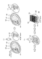
- FIG. 1 is a diagram showing a method of manufacturing a three-dimensional integrated circuit using WtW using Comparative Example 1.
- FIG. 2 is a diagram showing a method of manufacturing a three-dimensional integrated circuit by SA-MCtW using Comparative Example 2.
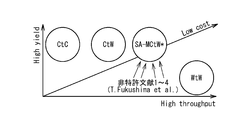
- FIG. 3 is a diagram showing the relationship between the throughput and yield of each manufacturing method of a three-dimensional integrated circuit.
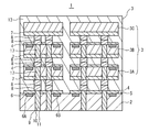
- FIG. 4 is a cross-sectional view showing the structure of an integrated circuit three-dimensionally integrated in this embodiment.
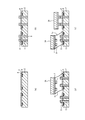
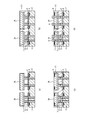
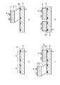
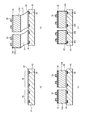
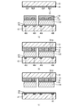
- FIG. 5A to FIG. 5D are cross-sectional views illustrating a method for manufacturing a three-dimensional integrated circuit according to this embodiment.
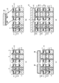
- FIG. 6A to FIG. 6D are cross-sectional views showing a method for manufacturing a three-dimensional integrated circuit according to this embodiment.
- FIGS. 7D are cross-sectional views illustrating a method for manufacturing a three-dimensional integrated circuit according to this embodiment.
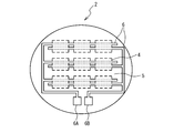
- FIG. 8 is a plan view of an interposer substrate on which an electrode for electrostatic attraction is formed.
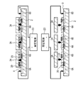
- FIG. 9 is a schematic diagram for explaining voltage application in electrostatic attraction.
- FIG. 10 is a cross-sectional view showing the structure of another three-dimensional integrated circuit manufactured using the chip support substrate of this embodiment.
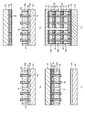
- FIG. 11A to FIG. 11D are flowcharts for explaining an example of the HSA-CtW process of the first modification of the present embodiment.
- FIG. 12A to FIG. 12D are flowcharts for explaining an example of the HSA-CtW process of the first modification of the present embodiment.
- FIG. 13A to 13D are flowcharts for explaining an example of the HSA-CtW process of the first modification of the present embodiment.
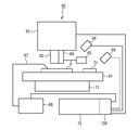
- FIG. 14 is a block diagram showing a configuration of an assembly apparatus used for hybrid assembly that performs electrostatic adsorption together with self-organized adsorption.
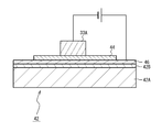
- FIG. 15 is a cross-sectional view showing an example of the configuration of the chip support substrate.
- FIG. 16 is a diagram schematically showing an optical image of a chip bonded by the assembly apparatus.
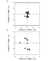
- FIG. 17A and FIG. 17B are diagrams showing the alignment accuracy of the chip, FIG. 17A is the present embodiment, and FIG. 17B is a comparative example.
- FIG. 18 is a diagram schematically showing an optical image of the chip support substrate.
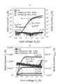
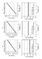
- FIGS. 21A and 21B are graphs showing the characteristics of the MOSFET.
- FIG. 21A shows the I D -V G characteristics
- FIG. 21B shows the I D -V D characteristics.
- 22 (a) to 22 (d) are diagrams showing a self-assembled chip after electrostatic temporary bonding, and FIG.
- FIG. 22 (a) is a diagram showing the surface after electrostatic temporary bonding.
- 22 (b) is the surface after transfer from the chip support substrate to the adhesive wafer
- FIG. 22 (c) is the surface after multi-chip thinning with a thickness of 140 ⁇ m to 25 ⁇ m
- FIG. 22 (d) is the self-organization. It is a figure which shows typically the SEM image of the cross section which formed Si via
- FIGS. 23 (a) to 23 (c) are diagrams showing current (upper figure) and resistance characteristics with respect to applied voltage of a wiring pattern called Daisy Chain in which a large number of micro-bumps made of Cu / AgSn are connected in series.
- FIG. 23 shows an image of a Cu / AgSn microbump bonded through a non-conductive film
- the lower figure is a TEM image
- the upper figure is a map of X-ray analysis.
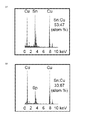
- 25 (a) and 25 (b) are diagrams showing X-ray analysis spectra at positions p and q shown in the lower diagram of FIG.
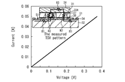
- FIG. 26 is a diagram showing IV characteristics of a wiring pattern called Daisy Chain in which a large number of micro-bumps with a pitch of 30 ⁇ m are connected in series.
- FIG. 27 (a) and 27 (b) are diagrams showing infrared images.
- FIG. 27 (a) shows a state after transfer to an adhesive wafer
- FIG. 27 (b) shows a semiconductor wafer serving as a target wafer via NCF. After the transfer.
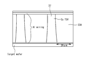
- FIG. 28 is a view showing an SEM image of a cross section after a thin chip which is 3D laminated by HSA-CtW and transferred from a bonded wafer to another target wafer is transferred.
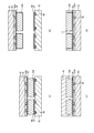
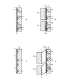
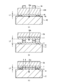
- FIGS. 29A to 29D are cross-sectional views illustrating a method for manufacturing a three-dimensional integrated circuit according to the second modification.
- FIG. 30A to FIG. 30D are cross-sectional views illustrating a method for manufacturing a three-dimensional integrated circuit according to Modification 2.
- 31D are cross-sectional views showing a method for manufacturing a three-dimensional integrated circuit according to Modification 2.
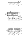
- 32 (a) to 32 (d) are cross-sectional views illustrating a method for manufacturing a three-dimensional integrated circuit according to Modification 3.
- FIG. 33A to FIG. 33D are cross-sectional views illustrating a method for manufacturing a three-dimensional integrated circuit according to Modification 3.
- 34A to 34D are cross-sectional views illustrating a method for manufacturing a three-dimensional integrated circuit according to Modification 3.
- FIGS. 35A to 35C are cross-sectional views when the chip is adsorbed to the chip support substrate.
- FIG. 36A to FIG. 36C are cross-sectional views showing a method for manufacturing a three-dimensional integrated circuit according to Modification 4.
- FIG. 37C are cross-sectional views showing a method for manufacturing a three-dimensional integrated circuit according to Modification 4.
- FIG. 38A to FIG. 38C are cross-sectional views showing a method for manufacturing a three-dimensional integrated circuit according to Modification 4.
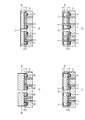
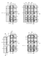
- 39A is a plan view of the chip support substrate
- FIGS. 39B and 39C are cross-sectional views corresponding to AA.
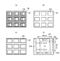
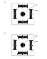
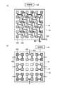
- FIG. 40A and FIG. 40B are plan views showing another example of the chip support substrate.
- Comparative Example 1 is an example of a method for manufacturing a three-dimensional integrated circuit using CtW.
- FIG. 1 is a diagram illustrating a method of manufacturing a three-dimensional integrated circuit using Comparative Example 1.
- a number of good chips (Known Good Dies, hereinafter referred to as KGD chips) 101 are attached to a tape 109 attached to a dicing frame 107.
- a broken line 108 is a dicing line.
- the pick-up tool 111 vacuum-sucks the chip 101 and picks up from the tape 109.
- the pickup tool 111 conveys the chip 101 onto the substrate 102 on which an integrated circuit or the like is formed.
- the chip 101 is mechanically positioned on the substrate 102 with a desired layout with high accuracy.
- the chip 101 is fixed on the substrate 102 via an adhesive.
- the pickup tool 111 fixes the next chip 101 on the substrate 102. In this way, the chips 101 are fixed to the substrate 102 one by one.
- the pickup tool 111 vacuum-sucks the chips 103 and conveys them to the top of the chips 101.
- the chip 103 is positioned with high accuracy and fixed on the chip 101.
- the chips 103 are fixed on the chip 101 one by one.
- the same process is repeated for the third and subsequent KGD chips 104.
- a silicon through electrode (called Through Silicon Via, TSV) penetrating the chips 101 and 103 vertically is formed.
- TSV Through Silicon Via
- the pickup tool 111 is bonded to the substrate 102 by a chip assembly method in which the chip 101 is adsorbed and desorbed.
- Comparative Example 2 is an example of a method for manufacturing a three-dimensional integrated circuit using SA-MCtW.
- FIG. 2 is a diagram illustrating a method of manufacturing a three-dimensional integrated circuit using the second comparative example.
- the single chip pickup tool 111 that transports the chips 101 one by one temporarily places the chips 101 on the base 112 one by one.
- the multi-chip pickup tool 113 that transports the plurality of chips 101 transports the plurality of chips 101 temporarily placed on the substrate 112 onto the substrate 102.
- the middle figure is an enlarged view of the substrate 102.
- a plurality of hydrophilic regions 110 and hydrophobic regions 120 are provided on the upper surface of the substrate 102.
- the liquid 114 is disposed on the plurality of hydrophilic regions 110 by dropping droplets on the plurality of hydrophilic regions 110.
- a non-defective chip 101 is placed on the liquid 114. When the liquid 114 evaporates, the chip 101 is adsorbed on the substrate 102. At this time, the chip 101 adsorbs to the hydrophilic region 110 in a self-organized manner due to the surface tension of the liquid 114.
- the chip 101 is thermocompression bonded onto the substrate 102 which is a wafer.
- the chip 103 is fixed on the chip 101 and the chip 104 is fixed on the chip 103.
- Comparative Example 2 both high throughput and high yield requirements are satisfied.
- a high-cost multichip pickup tool 113 is used to assemble a plurality of chips 101 on the liquid 114.
- the chip 101 is adsorbed to the substrate 102 by the surface tension of the liquid 114, the adsorption of the chip 101 to the substrate 102 is not sufficient. For this reason, in the subsequent process, careful work is performed so as to suppress the movement of the chip 101. Therefore, productivity is low.
- the chip 101 is aligned with the substrate 102 by the surface tension of the liquid 114, the alignment accuracy of the chip 101 to the substrate 102 is low. For this reason, productivity is low.
- FIG. 3 is a diagram showing the relationship between the throughput and yield of each manufacturing method of a three-dimensional integrated circuit.
- the above-described CtC, CtW (Comparative Example 1), and SA-MCtW (Comparative Example 2) are all methods in which chips having different functions are made into three-dimensional integrated circuits, and yield is high. However, the throughput is low. On the other hand, WtW has a high yield but a low yield.
- FIG. 4 is a cross-sectional view showing the structure of the integrated circuit 1 that is three-dimensionally integrated in the present embodiment.
- the three-dimensional (3D) integrated integrated circuit 1 includes a plurality of chips 3 ⁇ / b> A, 3 ⁇ / b> B, and 3 ⁇ / b> C stacked in a three-dimensional manner as a chip 3 on a chip support substrate 2. It has a chemical structure.
- the chip 3 is a semiconductor integrated circuit chip, an array chip of a light emitting element, or the like that is determined as a non-defective product by a predetermined test, and is also referred to as a KGD (Known Good Die) chip.
- the chip support substrate 2 is provided with a lyophilic region 4 capable of adsorbing the chip 3A in a self-organized manner via a liquid and a region 5 having a lower lyophilic property than the lyophilic region 4, and electrostatically An electrode 6 for adsorption is formed.
- the lyophilic region 4 and the region 5 having a lower lyophilic property than the lyophilic region differ in wettability (contact angle when a liquid is dropped on the region).
- the lyophilic region 4 is formed of a layer and the region 5 is shown as a region where no layer is formed.
- the lyophilic region 4 and the region 5 may be formed of layers.
- the liquid may contain an additive in order to increase the surface tension.
- an inorganic liquid or an organic liquid can be used, and water, glycerin, acetone, alcohol, SOG (Spin On Glass), or the like can be used.
- the lyophilic region 4 is described as the hydrophilic region 4, and the region 5 having a lower lyophilic property is described as the hydrophobic region 5. The same applies to the following modifications.
- the chip support substrate 2 means a substrate for supporting a three-dimensional structure in which chips composed of a single layer or a plurality of circuit layers are stacked, and a semiconductor, glass, ceramic, plastic, interposer substrate, or the like is used. It can.
- glass quartz glass or Pyrex (registered trademark) glass can be used.
- ceramic alumina or aluminum nitride can be used.
- interposer substrate an epoxy substrate or a glass fiber-containing epoxy substrate (glass epoxy substrate) can be used.
- An interposer substrate may refer to a bare silicon wafer or glass wafer in which no integrated circuit is formed, but the material of the interposer substrate is not limited.
- the chip support substrate 2 has a hydrophilic region 4 covered with a hydrophilic material and a hydrophobic region 5 in which the periphery of the hydrophilic region 4 is covered with a hydrophobic material.
- the hydrophilic region 4 is a region for accurately aligning the plurality of KGD chips 3 by the self-organizing function, and is a mounting region where the chips are adsorbed.
- the size and shape of the hydrophilic region 4 are substantially the same as those of the chip 3A. Thereby, the chip 3A is aligned with the hydrophilic region 4 by the surface tension of the liquid.
- the chip support substrate 2 is provided with an electrode 6 composed of an anode 6A and a cathode 6B, for example, via an insulating film under a hydrophilic material (for example, an insulating film) so that the chip 3 can be electrostatically attracted and fixed. ing.
- the electrode 6 is, for example, a comb electrode.
- the chip support substrate 2 of the present embodiment is characterized in that the KGD chip 3 can be three-dimensionally stacked using the chip support substrate 2 on which the comb electrodes 6 are arranged.
- a high voltage of 100 V to several hundreds V or higher is applied to the comb-teeth electrode 6 in order to collect and fix the chips 3 collectively.
- the chip support substrate 2 (for example, an interposer substrate) is a substrate on which the chip 3 on which an LSI made of a semiconductor is mounted is directly mounted.
- a substrate made of plastic or resin can be used as the chip support substrate 2.
- the chip support substrate 2 is used for connection to various printed boards (not shown) via solder bumps or solder balls (not shown) formed on the lower surface of the chip support board 2.
- Micro bumps 8 are formed on the upper surface of the chip support substrate 2.
- the solder bumps or solder balls and the micro bumps 8 are electrically connected through the chip support substrate through electrodes 11.
- the chip support substrate through electrode 11 is an electrode 10 embedded in the through hole 9.
- the chip support substrate through electrode 11 is also simply referred to as a via.
- the chip 3A is a chip on which the above-described semiconductor LSI or the like is mounted, and an insulating layer 7 and the like and micro bumps 8 are formed on the lower surface thereof.
- a hydrophilic region 4 and a hydrophobic region 5 (not shown) that can adsorb the chip 3A in a self-organized manner are formed on the upper surface of the chip 3A, and an electrode 6 for electrostatic adsorption is formed. .
- micro bumps 8 are formed on the chip 3A.
- the micro bumps 8 formed on the lower surface and the upper surface of the chip 3A are electrically connected via the Si through electrode 17.
- the micro bumps 8 formed on the chip support substrate 2 and the micro bumps 8 formed under the chip 3A are fixed.
- the chip support substrate 2 and the chip 3A are electrically connected via the micro bumps 8.
- the semiconductor is made of a single element semiconductor such as Si or Ge or a compound semiconductor.
- the chip 3 will be described as being made of Si.
- the chip 3B and the chip 3C have the same configuration as the chip 3A.
- the chip 3A, the chip 3B, and the chip 3C have functions of, for example, a microprocessor, various memories, an image sensor, a light emitting element array, a micromachine (MEMS: Micro Electro Mechanical System), and the like.
- the chip 3A, the chip 3B, and the chip 3C may include chips having the same function or different functions.
- each chip in which the chip 3A, the chip 3B, and the chip 3C are stacked may have a different function.
- FIG. 5A to FIG. 7D are cross-sectional views illustrating a method for manufacturing the integrated circuit 1 three-dimensionally integrated according to this embodiment.
- A Production of Interposer Substrate
- an electrostatic adsorption electrode 6 is formed on a chip support substrate 2 which is an interposer substrate.
- Al / W is vapor-deposited on the chip support substrate 2, and then the pattern of the electrode 6 is formed by lithography and etching of Al / W RIE (Reactive Ion Etching).
- a portion where the chip 3A is adsorbed is defined as a hydrophilic region 4, and another portion where the chip 3A is not adsorbed is defined as a hydrophobic region 5.
- the hydrophilic region 4 can be formed of an oxide film such as SiO 2 .
- the hydrophilic region 4 can be formed of Si 3 N 4 in addition to SiO 2 .
- the hydrophilic region 4 can be formed of a two-layer film of aluminum and alumina (Al / Al 2 O 3 ) and a two-layer film of tantalum and tantalum oxide (Ta / Ta 2 O 5 ).
- the hydrophobic region 5 can be formed by a film made of, for example, fluorocarbon.
- the hydrophobic region 5 is made of single crystal silicon (Si), epoxy resin, fluorine resin, silicone resin, Teflon (registered trademark) resin, polyimide resin, resist, wax, or BCB (benzocyclobutene) having hydrophobicity. Or the like.
- the hydrophobic region 5 is formed on the chip mounting surface of the interposer substrate that is the chip support substrate 2 by using polycrystalline silicon, amorphous silicon, fluorine resin, silicone resin, Teflon (registered trademark) resin, polyimide resin, resist, wax, or benzocyclo. It may be formed by covering with butene (BCB) or the like.
- FIG. 5 (b) Formation of Through Electrode for Interposer Substrate
- a through hole 9 penetrating the substrate is formed at a predetermined position of the chip support substrate 2, and then a conductive material such as metal is formed in the through hole 9.
- a through electrode 11 for an interposer substrate is formed by embedding a body electrode.
- Micro bumps 8 made of a conductor such as metal are formed on the top of the through holes 9.
- C Self-Assembly As shown in FIG. 5 (c), the thinned chip 3A is adsorbed in a self-organizing manner to the hydrophilic region 4 on which the chip 3A of the chip support substrate 2 is placed. That is, water is dropped as the liquid 15 on the hydrophilic region 4.
- the chip 3 ⁇ / b> A is placed on the liquid 15. As the liquid 15 evaporates, the chip 3 ⁇ / b> A is adsorbed onto the hydrophilic region 4. Next, as shown in FIG. 5D, another chip 3 ⁇ / b> A is adsorbed in a self-organized manner in another hydrophilic region 4.
- the material of the resin mold 13 is, for example, an epoxy resin.
- the resin mold 13 may not be formed, and may be formed after the chips 3A to 3C are stacked. In this case, the hydrophobic region may not be formed.
- the process of resin molding between the chips 3 is a process that can be omitted if unnecessary.
- the electrostatic adsorption electrode 6 is formed on the surface of the chip 3A. Formation of the electrode 6 for electrostatic attraction can be performed in the same manner as in the step (A). In FIG. 6C, the electrode 6 is embedded in the chip 3A, but the electrode 6 may be formed on the flat surface of the chip 3A.
- the resin mold 13 is formed on the upper surface of the chip 3A, the surface of the chip 3A on which the resin mold 13 is formed is exposed, and then the electrode 6 for electrostatic adsorption is formed.
- FIG. 6D Formation of Si Through Electrode and Micro Bump on Chip 3A
- Micro bumps 8 are formed on the chip 3A.
- the TSV 17 and the micro bumps 8 can be formed in the same manner as in the step (B).
- step (C) Electrostatic Adsorption of Chip 3B As shown in FIG. 7C, the chip 3B adsorbed in a self-organized manner is electrostatically adsorbed to the chip 3A. This step can be performed in the same manner as in step (D).
- the chips 3A and 3B, and further the chip 3C and the like can be stacked on the chip support substrate 2.
- the insulating layer 7 and the micro bumps 8 are formed on the lower surface side of the chip 3C. TSV17 may not be formed.
- the manufacturing method of the three-dimensional integrated circuit 1 according to this embodiment is characterized in that the KGD chip 3 is dropped on a water droplet having a self-organizing function, or This is because a method of electrostatically attracting and fixing the plurality of KGD chips 3 to the chip support substrate 2 at once after being attached and released. According to this method, the three-dimensional integrated circuit 1 having a three-dimensional stacked structure can be manufactured with high yield, high productivity, high accuracy, and low cost.
- FIG. 8 is a plan view of the chip support substrate 2 on which the electrode 6 for electrostatic attraction is formed.
- the electrode 6 for electrostatic attraction is a so-called bipolar electrode composed of an anode 6A and a cathode 6B.
- An anode 6A and a cathode 6B are formed in the hydrophilic region 4.
- the bipolar electrode 6 is, for example, a comb electrode as shown in FIG. A positive voltage is applied to the anode 6A of the comb electrode 6 shown in FIG. 8, and a negative voltage is applied to the cathode 6B.
- the electrostatic force applied to the chip 3A using such a bipolar electrode 6 is given by the following equation (1).
- F bp is the electrostatic force generated by electrostatic bonding using the bipolar electrode 6
- A is the area of the comb electrode
- d is the distance between the electrode 6 and the chip 3
- ⁇ r is the relative dielectric constant.
- ⁇ 0 is the dielectric constant in vacuum
- V is the applied voltage.
- FIG. 9 is a schematic diagram for explaining voltage application in electrostatic adsorption.
- a high-voltage direct current (DC) voltage is applied between the anode 6 ⁇ / b> A and the cathode 6 ⁇ / b> B of the comb-tooth electrode using the high-voltage power supply 23.
- a positive voltage is applied to the anode 6A, and a negative voltage is applied to the cathode 6B.
- Electric field lines are formed on the anode 6A upward as indicated by an arrow 20. Electric field lines are formed downward on the cathode 6B as indicated by an arrow 20.
- a plurality of chips 3A, 3B, and 3C are provided on the chip support substrate 2.
- the hydrophilic region 4 formed on the chip support substrate 2 and the chips 3A and 3B is formed of an oxide film. Therefore, even if the hydrophilic region 4 is formed, the chips 3A, 3B, and 3C of the integrated circuit 1 integrated three-dimensionally are not affected.
- the hydrophobic regions 5 formed on the chip support substrate 2 and the chips 3A and 3B are formed of a film made of fluorocarbon.
- the chips 3A, 3B, and 3C of the integrated circuit 1 integrated three-dimensionally are not affected. Furthermore, the electrostatic chucking electrodes 6 formed on the chip support substrate 2 and the chips 3A and 3B are insulated from the TSVs 11 and 17 via an insulator. Therefore, even if the electrode 6 is formed, the chips 3A, 3B, and 3C of the integrated circuit 1 that is three-dimensionally integrated are not affected.
- the chip 3 is adsorbed by the adsorption force of an aqueous solution having a self-organizing function. For this reason, the adsorbing force is very weak or too strong, and once the chip 3 is fixed, it cannot be peeled off, and there is a disadvantage that the yield of lamination by transfer is low.
- a plurality of KGD chips 3A are strongly and simultaneously attached to the chip support substrate 2 by using a self-organizing function and electrostatic interaction. Adsorption can be fixed. For this reason, productivity becomes high and positioning with high reliability is possible. Further, as shown in the lower diagram of FIG. 9, the chip 3 ⁇ / b> A can be easily peeled off from the chip support substrate 2 by applying a voltage having a polarity opposite to that of electrostatic adsorption to the electrode 6.
- FIG. 10 is a cross-sectional view showing the structure of a three-dimensional integrated integrated circuit 30 manufactured using the chip support substrate 42 according to the first modification of the present embodiment.
- the integrated circuit 30 three-dimensionally integrated has a structure in which chips 33A to 33C are three-dimensionally stacked on a Si wafer 32.
- An element formation region 34 is formed above each of the chips 33A, 33B, and 33C.
- a transistor or a light emitting element is formed.
- Micro bumps 38 are disposed through an interlayer insulating film (not shown) on the element formation region 34. Micro bumps 38 are formed on the lower surfaces of the chips 33A, 33B, and 35C.
- the micro bumps 38 formed on the Si wafer 32 and the micro bumps 38 formed on the lower surface of the chip 33A are joined. Thereby, the Si wafer 32 and the chip 33A are electrically and mechanically connected.
- the chip 33B is stacked on the chip 33A, and the chip 33C is stacked on the chip 33B.
- a TSV 37 penetrating the chips 33A, 33B, and 33C vertically is formed.
- the micro bumps 38 formed above and below the chips 33A and 33B are electrically connected through the TSV 37.
- an integrated circuit or an array of light emitting elements is formed on the semiconductor wafer 32.
- the semiconductor wafer 32 is, for example, a Si wafer. In the following description, the semiconductor wafer 32 is described as an Si wafer.
- a gap filling resin 39 is embedded between the plurality of micro bumps 38 formed on the Si wafer 32.
- a gap filling resin 39 is buried between the plurality of micro bumps 38 formed on the surface of the chip 33A facing the chip 33B, and the upper surface side of the chip 33A and the lower surface side of the chip 33B connect the micro bumps 38. Connected through.
- a gap filling resin 39 is embedded between the plurality of micro bumps 38 formed on the surface of the chip 33B facing the chip 33C, and the upper surface side of the chip 33B and the lower surface side of the chip 33C are microscopic. They are connected via bumps 38.
- the integrated circuit 30 that is three-dimensionally integrated is sealed with a resin mold 41.
- An integrated circuit is formed on the Si wafer 32.
- the Si wafer 32 may include a through electrode (not shown) and a micro bump on the lower surface of the Si wafer 32.
- the three-dimensionally integrated integrated circuit 30 is connected to an external circuit via a micro bump on the lower surface side of the Si wafer 32.
- FIG. 11A to FIG. 13D are flowcharts for explaining an example of the H (Hybrid) SA-CtW process of the first modification of the present embodiment, which will be sequentially described below.
- A As shown in FIG. 11A, first, the KGD chip 33A is directly selected from the wafer surrounded by the dicing frame. Next, a multichip carrier having a hydrophilic region and an electrode for electrostatic adsorption, that is, a chip support substrate 42 is placed on a stage 61 of an assembly apparatus 60 described later. A hydrophilic region 44 (lyophilic region) and a hydrophobic region 45 (region having low lyophilicity), which are bonding regions, are formed on the upper surface of the chip support substrate 42.
- the hydrophilic region 44 is formed by an insulating film, for example.
- An electrode 46 is formed under the insulating film in the hydrophilic region 44.
- the chip 33 ⁇ / b> A is released onto the liquid 15 which is a water droplet disposed in the hydrophilic hydrophilic region 44 formed on the chip support substrate 42.
- the An element forming region 34 is formed on the chip 33A, and micro bumps 38 are formed on the element forming region 34.
- FIG. 11C by repeating the above steps, many chips 33A are continuously and accurately arranged on the chip support substrate 42 in a self-organizing manner.
- a high voltage DC voltage is applied to the electrode 46. Thereby, the chip 33 ⁇ / b> A is temporarily bonded onto the chip support substrate 42.
- the chip support substrate 42 having the chips 33 ⁇ / b> A is aligned and temporarily bonded to the transfer support substrate 43.
- a wafer bonder is used for alignment.
- An adhesive layer 43A is coated on the transfer support substrate 43 (the lower surface in FIG. 12A).
- the transfer support substrate 43 coated with the adhesive layer 43 ⁇ / b> A is referred to as an adhesive wafer 43.
- the heat-resistant adhesive layer 43A used in this step is a new material and has been introduced for the first time.
- the new temporary bonding adhesive layer 43A can be easily peeled from the adhesive wafer 43 using a visible laser. This is the basic technique of this process.
- a large number of temporarily fixed chips 33 A are released from the chip support substrate 42 by discharging and moved to the adhesive wafer 43. That is, it is transferred.
- This process is called a first transfer.
- the chip support substrate 2 shown in FIGS. 5A to 7D becomes a part of the three-dimensional integrated circuit, but the chip support substrate 42 does not become a wafer of the integrated circuit 30 integrated three-dimensionally. .
- the chip support substrate 42 can be reused after the first transfer.
- a resin mold 41 is formed on the adhesive wafer 43 so as to cover the chip 33A.
- the resin mold 41 may not be formed, but may be formed after the chips 33A to 33C are stacked. In this case, the hydrophobic region is not formed.
- G Thinning process of multichip As shown in FIG. 12D, in this process, in order to adjust the thickness of the three-dimensional integrated circuit, a plurality of chips (multichips) 33A are formed as necessary. make it thin. Thinning of the multichip 33A is performed by grinding or CMP (Chemical Mechanical Polishing) from the back surface (upper surface in FIG. 12D) side of the chip 33A in which the element formation region 34 is not formed. The element forming region 34 of the chip 33A is protected by the adhesive wafer 43. The upper surface of the chip 33 ⁇ / b> A is exposed from the resin mold 41.
- TSV 37 and Micro Bump 38 As shown in FIG. 13A, a TSV 37 penetrating the chip 33A vertically is formed. Micro bumps 38 are formed on the upper surface of the chip 33A.
- An element formation region 34 is formed in the upper part (lower part in FIG. 13B) of the semiconductor wafer 32.
- Micro bumps 38 are formed on the element formation region 34.
- the micro bumps 38 of the semiconductor wafer 32 and the micro bumps 38 of the chip 33A are thermocompression bonded by a thermobonding wafer bonding apparatus.
- a stage of a bonding apparatus for thermocompression bonding is performed by a thermal process in which the stage is heated to, for example, 50 ° C. to 250 ° C. and then cooled to 50 ° C.
- a target LSI or a light emitting element array is mounted on the semiconductor wafer 32.
- a gap filling resin 39 is embedded between the plurality of micro bumps 38 of the semiconductor wafer 32.
- the gap filling resin 39 is made of an epoxy resin or the like.
- the gap filling resin 39 is also called a non-conductive film (NCF).
- the semiconductor of the semiconductor wafer 32 will be described as Si.
- (J) Separation Process of Chip 33A from Bonded Wafer 43 As shown in FIG. 13C, after the micro bumps 38 of the Si wafer 32 on which the target LSI is mounted and the micro bumps 38 of the chip 33A are thermocompression bonded. Thus, the chip 33 ⁇ / b> A is peeled off from the bonded wafer 43 using the vacuum suction force of the wafer bonding apparatus. The bonded wafer peeled off after the micro bumps 38 of the chip 33A are thermocompression bonded to the Si wafer 32 on which the target LSI is mounted can be reused.
- the substrate of the adhesive wafer 43 on which the adhesive layer 43A is placed can be used repeatedly. That is, the substrate can be reused by forming a new adhesive layer 43A on the substrate after the adhesive layer 43A of the used adhesive wafer 43 has been peeled off by spin coating or the like.
- the adhesive layer 43A may be peeled using heating, a peeling treatment with a solvent, light, an ultraviolet laser, or the like, or a combination thereof.
- chip-wafer 3D integration based on hybrid self-organization in the method of manufacturing a three-dimensional integrated circuit according to the present embodiment and its modification 1
- chips 3A to 3C driven by surface tension driving of the liquid 15 are used.
- the self-organized adsorption of 33A to 33C and the provisional bonding technology of a plurality of chips 3A to 3C or 33A to 33C by electrostatic adsorption are combined.
- the temporary bonding technique of a plurality of chips 3A to 3C or 33A to 33C by electrostatic adsorption enables direct bonding without stress of the chips adsorbed in a self-organized manner.
- the alignment accuracy is as high as about 1 ⁇ m. Therefore, it is possible to maintain high alignment accuracy without causing lateral displacement.
- the three-dimensional integrated circuit 30 using the micro bumps 38 made of Cu / SnAg and the through electrodes 11 and 17 using Cu good electrical characteristics can be obtained.
- the production throughput can be increased without using the high-cost multi-chip pickup tool of the comparative example 2. Thereby, a chip assembly of 10,000 chips / hour can be realized.
- the integrated circuit 1 or 30 integrated three-dimensionally according to the present embodiment and the modification 1 thereof it is possible to stack the chips 3A to 3C or 33A to 33C on the chip support substrate 2 or the semiconductor wafer 32 with high positional accuracy. Because it is manufactured with high throughput, it is low cost.
- FIG. 14 is a block diagram showing a configuration of an assembly apparatus 60 used for a hybrid assembly that performs electrostatic adsorption together with self-organized adsorption. As shown in FIG.
- the assembly device 60 includes a stage 61 on which the chip support substrate 2 or 42 is placed, a transfer robot 63 having pickup tools 62 of chips 3A to 3C or 33A to 33C, From the precision droplet discharge unit 64, the droplet supply unit 65, the electrostatic suction power source 66, the probe 67 that supplies the electrostatic suction power source 66 to the substrate, the first camera 68, and the second camera 69
- the chip support substrate and the imaging unit for observing the chip, a chip storage tray 71, a control unit 72, and the like are included.
- the stage 61 may further include an inclination correction mechanism 73.
- the assembly apparatus 60 can be used for manufacturing the three-dimensional integrated circuit 1 shown in FIG. 4 and the three-dimensional integrated circuit 30 shown in FIG.
- the needle of the probe 67 connected to the electrostatic attraction power source 66 contacts the electrostatic attraction electrode 6 or 46 formed on the interposer substrate 2 or the chip support substrate 42, and the electrostatic attraction power source 66 is applied. Is done.
- a plurality of probes 67 may be provided corresponding to the anode 6A and the cathode 6B.
- the transfer robot 63 is a transfer robot that transfers the hydrophilic droplet and the chip 33 to the substrate.
- the transfer robot 63 includes a high-precision droplet discharge unit 64 that supplies hydrophilic droplets to the substrate, and a pickup tool 62 for the chip 33.
- the transfer robot 63 is a so-called industrial robot, and an XY robot or a scalar robot that performs transfer in two dimensions can be used. In the following description, the transfer robot 63 is described as a scalar robot.
- the high-precision droplet discharge unit 64 is connected to the droplet supply unit 65, and the control unit 72 controls the amount of droplets and the discharge time for discharging the droplets.
- the pick-up tool 62 of the scalar robot 63 includes a chuck for sucking the chips 3A to 3C or 33A to 33C, and the position thereof is monitored by the first and second high-resolution cameras 68 and 69. .
- the chuck for adsorbing the chips 3A to 3C or 33A to 33C is, for example, a vacuum chuck.
- the first and second cameras 68 and 69 are so-called high resolution cameras.
- the position of the pick-up tool 62 of the scalar robot 63 is first controlled by the monitoring of the first camera 68 disposed above the stage 61, and a predetermined position on the chip support substrate 2 or the chip support substrate 42, for example, A droplet made of pure water is discharged.
- the position of the pickup tool 62 of the scalar robot 63 is controlled by monitoring the second camera 69 disposed below the first high-resolution camera 68 and is controlled to move to the chip storage tray 71.
- the chips 3A to 3C or 33A to 33C in the chip storage tray 71 are sucked by the vacuum chuck.
- the positions of the vacuum-sucked chips 3A to 3C or 33A to 33C are controlled by the monitoring of the first camera 68, and are transported to a predetermined location on the chip support substrate 2 or the chip support substrate 42 to stop vacuum suction.
- the liquid droplets are temporarily bonded to the locations where the droplets on the chip support substrate 2 or the chip support substrate 42 are dropped.
- the chips 3A to 3C, or 33A to 33C become the chip support substrate 2 or the chip. It is electrostatically attracted to the support substrate 42.
- the control unit 72 controls the operation of the hybrid self-organizing assembly device 60 described above.
- the control unit 72 includes a computer, a display device, a storage device, and the like (not shown).
- the computer controls the scalar robot 63, the high-precision droplet discharge unit 64, the droplet supply unit 65, the electrostatic attraction power source 66, the first and second cameras 68 and 69, and the like via the interface circuit 72A. Is done.
- the chip support substrate 42 can be manufactured on a substrate 42A, which is a Si wafer, using a standard lithography method, a CVD (Chemical Vapor Deposition) method, an RIE method, or the like.
- FIG. 15 is a cross-sectional view showing an example of the configuration of the chip support substrate 42.
- the chip support substrate 42 includes a hydrophilic region 44 that is a bonding region in which the chip 33 ⁇ / b> A can be adsorbed in a self-organizing manner, and an electrode 46 for electrostatic adsorption.
- a DC voltage for electrostatic adsorption is applied to the electrode 46 and the chip 33A itself to be adsorbed.
- Such an electrode is called a unipolar electrode.
- the electrostatic force applied to the chip 33A is expressed by the following equation (2).
- F up is an attracting force generated by electrostatic bonding when the unipolar electrode 46 is used
- A is an area of the electrode 46
- d is a distance between the electrode 46 and the chip 33A
- ⁇ r is a relative dielectric constant
- ⁇ 0 is the dielectric constant in vacuum
- V is the applied voltage. Accordingly, the electrostatic attraction force increases as the surface voltage increases.
- a thermal oxide film 42B having a thickness of 100 nm is formed on a p-type Si substrate 42A having a resistivity of 10 to 15 ⁇ ⁇ cm to which boron is added.
- An Al / W film is deposited on the thermal oxide film 42B by sputtering.
- the Al / W film is patterned by a lithography method.
- An electrode 46 is formed by the Al / W film.
- a plasma TEOS (Tetraethyl orthosilicate) oxide film having a thickness of 6 ⁇ m is deposited. Thereafter, the TEOS oxide film is etched to form a hydrophilic region 44.
- the performance of the assembly by picking and sucking is 0.3 seconds / chip (about 12,000 chips / hour) as a throughput. Is achieved.
- the HSA-CtW process was performed by the processes shown in FIGS. 11 (a) to 13 (d). Unless otherwise specified, the three-dimensional integrated circuit is manufactured by the manufacturing method shown in FIGS. 11 (a) to 13 (d).
- the electrode 46 of the chip support substrate 42 was a bipolar type. The main parts used in the assembly device 60 are shown below.
- Scalar robot 63 YMA600, YK600X High-precision droplet discharge unit 64, droplet supply unit 65: manufactured by Iwashita Engineering Co., Ltd., AD3000CLLL
- Electrostatic adsorption power source 66 Matsuda Precision Co., Ltd., HECA-3B10X2LPo Probe 67: 708fT-008 manufactured by Nihon Micronics Tilt correction mechanism 73: Automatic precision leveling table (Auto Stage AS-21) manufactured by Sakamoto Electric Mfg. Co., Ltd.
- First camera 68 and second camera 69 manufactured by Keyence Corporation, cameras CV-200M and CV-5500 controllers
- the side wall of the through hole was covered with a SiO 2 film.
- the formed SiO 2 film was coated with TiN serving as a barrier layer and copper (Cu) by sputtering.
- Cu plugs were formed in the through holes by Cu plating, and micro bumps 38 made of Cu and Ag / Sn were formed on the surface of the self-organized chip 33A.
- the micro bumps 38 were formed by processes such as Cu plating and Ag / Sn deposition.
- FIG. 16 is a diagram schematically showing an optical image of the chip 33A bonded by the assembly device 60. As shown in FIG. As shown in FIG. 16, four types of chips having a thickness of 140 ⁇ m and a size of 3 mm square, 5 mm square, 4 mm ⁇ 9 mm square, and 10 mm square are formed on an 8-inch Si substrate serving as the chip support substrate 42. It can be seen that 33A is assembled into the self-organization continuously and accurately.
- FIG. 17 (a) and 17 (b) are diagrams showing the alignment accuracy of the chip
- FIG. 17 (a) is the present example
- FIG. 17 (b) is the comparative example 2.
- FIG. 17A in the case of the present embodiment, it can be seen that the alignment accuracy of the chip 33A is within 1 ⁇ m.
- FIG. 17B it can be seen that in Comparative Example 2 in which electrostatic attraction is not performed, the chip alignment accuracy varies as ⁇ 3 ⁇ m.
- the chip can be fixed in a process such as chip transfer by electrostatically adsorbing the chip 33A to the chip support substrate. For this reason, alignment accuracy can be improved as compared with Comparative Example 2.
- FIG. 18 is a diagram schematically showing an optical image of the chip support substrate 42.
- the hydrophilic region 44 is formed over the region where the electrode 46 is formed.
- a part of the hydrophilic region 44 is indicated by a broken line.
- the chip support substrate 42 has a hydrophobic structure in which a comb-tooth electrode 46 made of Al / W, a hydrophilic hydrophilic region 44 made of an oxide film, and a hydrophobic fluorocarbon surrounding it are formed. And a sex region 45.
- an anode 46A and a cathode 46B are provided in the hydrophilic region 44.
- a DC high voltage of 100 V or 200 V is applied between the two electrode pads connected to the anode 46A and the cathode 46B made of Al / W.
- the DC voltage generates an electrostatic attraction force.
- the electrostatic attraction force is expressed by the electrostatic force of the above formula (1).
- FIG. 19A and FIG. 19B are diagrams in which the influence of parameters on the electrostatic attraction force is examined.
- FIG. 19A shows the influence of an applied voltage, which is a DC voltage applied between the anode 64A and the cathode 64B, on the electrostatic attraction force.
- FIG. 19B shows the influence of the annealing temperature after applying the voltage on the electrostatic adsorption force.
- the horizontal axis represents the holding time (minutes) after voltage is applied between the anode 64A and the cathode 64B
- the vertical axis represents the voltage between the anode 46A and the cathode 46B.
- the voltage corresponds to the electrostatic attraction force.
- FIG. 19A are 100V, 200V, 300V and 400V.
- the annealing temperatures in FIG. 19B are 100 ° C., 200 ° C., and 300 ° C., and the annealing time is 10 minutes.
- the applied voltage is 200V.
- data not annealed (not baked) is also shown.
- FIG. 19A it can be seen that when the applied voltage is 100 V and 200 V, the electrostatic attraction force is maintained for up to 15 minutes.
- FIG. 19B it can be seen that the electrostatic attraction force is not affected even at the annealing temperature of 100 ° C. after the electrostatic temporary bonding.
- FIG. 20 (a) and 20 (b) are diagrams in which the influence of parameters on the electrostatic adsorption force by the unipolar electrode 46 is examined.
- FIG. 20 (a) shows the influence of the applied voltage
- FIG. Shows the effect of temperature.
- 20A and 20B the horizontal axis represents the retention time (minutes), and the vertical axis represents the voltage.
- the applied voltage is 100V and 200V
- the thermal oxide film 42B formed on the substrate 42A is not in contact with the p-TEOS oxide film.
- FIG. 20B it can be seen that the electrostatic attraction force is not affected even at the annealing temperature of 100 ° C. after the electrostatic temporary bonding.
- the thermal oxide film 42B formed on the substrate 42A is in contact with the p-TEOS oxide film (hydrophilic region 44).
- FIG. 21A and FIG. 21B are diagrams showing the characteristics of the MOSFET.
- the gate length and gate width of the MOSFET are both 10 ⁇ m.
- the thickness of the gate oxide film is 3 nm.
- FIG. 21A and FIG. 21B show the characteristics after applying a voltage of 100 V to the electrode 46 for 10 minutes before applying a voltage to the electrode 46 and then applying a voltage of 100 V to the electrode 46 for 30 minutes. Show.
- FIG. 21A and FIG. 21B show the characteristics after applying a voltage of 100 V to the electrode 46 for 10 minutes before applying a voltage to the electrode 46 and then applying a voltage of 100 V to the electrode 46 for 30 minutes. Show.
- FIG. 21A shows drain current-gate voltage (I D -V G ) characteristics and gate current-gate voltage (I G -V G ) characteristics when the drain voltages are 1.0 V and 2.5 V.
- FIG. 21B shows drain current-drain voltage (I D -V D ) characteristics and body current-drain voltage characteristics when the gate voltages are 1.5V, 2.0V and 2.5V.
- the characteristics are the same before voltage application and after voltage application for 10 minutes and 30 minutes.
- the threshold voltage, gate leakage current, output characteristics, and substrate current of the MOSFET are not affected by the DC voltage applied to the electrode 46.
- FIGS. 22 (a) to 22 (d) are diagrams showing the self-assembled chip 33A after electrostatic temporary bonding.
- 22A shows the surface of the chip support substrate 42 after electrostatic temporary bonding
- FIG. 22B shows the surface of the adhesive wafer 43 after transfer from the chip support substrate 42 to the adhesive wafer 43
- FIG. 22C shows the surface of the adhesive wafer 43 after the thinning of the multi-chip having a thickness of 140 ⁇ m to 25 ⁇ m.
- FIG. 22D shows a Si via 37B (Si Via 37B) using a Bosch process on the self-organized chip 33A. It is a figure which shows typically the SEM (Scanning Electron Microscope) image of the cross section in which the chip
- the chip 33A self-assembled by discharge is applied to an adhesive wafer 43 on which a thermally stable adhesive layer 43A having a thickness of 15 ⁇ m is spin-coated. You can see that it is transcribed.
- a deep via 37B having a diameter of 10 ⁇ m and a depth of about 25 ⁇ m is formed in the vertical direction of the transferred chip 33A.
- the via 37B is formed by a Bosch process.
- the via 37B is formed by using ICP (Inductively Coupled Plasma) -RIE using SF 6 and C 4 F 8 gas.
- the photoresist 37A is peeled off after the via 37B is formed.
- FIG. 23 (a) to 23 (c) show the characteristics of current (upper figure) and resistance (lower figure) with respect to the applied voltage of a wiring pattern called Daisy Chain in which a large number of Cu / AgSn microbumps 38 are connected in series.
- FIG. The pitch of the micro bumps 38 is 40 ⁇ m in FIG. 23A, 60 ⁇ m in FIG. 23B, and 80 ⁇ m in FIG.
- FIGS. 23A to 23C it can be seen that the micro bumps 38 made of Cu / AgSn are electrically connected to each other, and the resistance is sufficiently small.
- a wiring pattern with a pitch of 40 ⁇ m has 5096 bumps connected thereto, and the bump / wiring resistance per bump is 67.5 m ⁇ .
- the wiring pattern with a pitch of 60 ⁇ m has 732 bumps connected thereto, and the resistance of the bump and wiring per bump is 173 m ⁇ .
- the wiring pattern with a pitch of 80 ⁇ m has 564 bumps connected thereto, and the resistance of the bump and wiring per bump is 2705 m ⁇ .
- These resistors do not include TSV resistors.
- FIG. 24 is a schematic diagram of an image of a micro bump 38 made of Cu / AgSn bonded via a gap filling resin 39 which is a non-conductive film.
- the lower diagram of FIG. 24 is a schematic diagram of a TEM (Transmission Electron Microscope) image
- the upper diagram of FIG. 24 is a map diagram of X-ray analysis.
- 25 (a) and 25 (b) are diagrams showing X-ray analysis spectra at the positions p and q shown in the lower diagram of FIG. X-ray analysis was performed using an energy dispersive (EDX) detector.
- EDX energy dispersive
- FIG. 26 is a diagram showing current I-voltage V characteristics of a wiring pattern called Daisy Chain in which a large number of micro-bumps 38 with a pitch of 30 ⁇ m are connected in series.
- the resistance R1 is the resistance of the wiring 31 formed on the wafer 32
- the resistance R2 is the resistance of the micro bump 38 and the TSV 37 formed on the chip 33A
- the resistance R3 is the resistance of the wiring 31 formed on the chip 33A.
- Cu-TSV 37 is formed at a high yield
- the IV characteristic is a resistive electrode.
- FIG. 27A and FIG. 27B schematically show infrared images. An alignment mark 82 and a misalignment measurement pattern 84 are shown.
- 27A is a schematic view of an image after transfer to the adhesive wafer 43
- FIG. 27B is a schematic view of an image after transfer to the semiconductor wafer 32 serving as a target wafer via the NCF. From FIG. 27A and FIG. 27B, it can be seen that the alignment accuracy is within 1 ⁇ m after the multichip 33 is transferred twice by self-assembly and thermocompression bonding.
- FIG. 28 is a view showing an SEM image of a cross section after a thin chip 33 that is 3D laminated by HSA-CtW and self-organized from the bonded wafer 43 to another target wafer 32 is transferred. As shown in FIG. 28, it can be seen that the KGD chip 33A is 3D laminated by HSA-CtW.
- Table 1 is a table comparing the manufacturing method of Modification 1 of this embodiment with the manufacturing method of the comparative example. From Table 1, it can be seen that according to the manufacturing method of Modification 1, the three-dimensional integrated circuit 30 can be manufactured with high throughput and high yield, and the cost is low.
- the throughput is an example in which 10,000 chips are formed on one wafer.
- the heating and cooling time required for the thermocompression bonding process is 20 minutes / wafer, and the chip alignment accuracy is less than 1 ⁇ m.
- the throughput of an assembly of 10,000 chips is about 1.2 hours.
- CtW of Comparative Example 1 and Comparative Example 2 it is possible to manufacture a high-mix and low-volume three-dimensional integrated circuit at a low cost.
- Modification 2 is an example in which the method of disposing the chip 33A on the liquid 15 is changed from Modification 1 shown in FIGS. 11 (a) to 13 (d).
- FIGS. 29A to 31D are cross-sectional views illustrating a method for manufacturing a three-dimensional integrated circuit according to Modification 2. Although the range of one three-dimensional integrated circuit is shown in the figure, for example, a plurality of chips 33A are arranged on the chip support substrate 42, the adhesive wafer or the semiconductor wafer 32 as shown in FIG.
- a chip support substrate 42 is prepared.
- the chip support substrate 42 mainly includes a substrate 51, an electrode 46, a hydrophilic region 44, and a hydrophobic region 45.
- a substrate 51 a semiconductor substrate or an insulator substrate can be used.
- the materials exemplified in FIG. 4 can be used.
- An electrode 46 is formed on the upper surface of the substrate 51.
- the material of the electrode 46 is, for example, a metal containing Au, Al, or Cu, or a conductor other than metal.
- a hydrophilic region 44 and a hydrophobic region 45 are formed on the upper surface of the chip support substrate 42.
- the hydrophilic region 44 is, for example, a hydrophilic layer and is an insulating film such as a silicon oxide film or a silicon nitride film.
- the materials described in FIG. 4 can be used as the hydrophilic region 44 and the hydrophobic region 45.
- a region other than the hydrophilic layer formed in the hydrophilic region 44 can be used as the hydrophobic region 45.
- the liquid 15 is appropriately applied onto the hydrophilic region 44. Since the liquid 15 is not adsorbed to the hydrophobic region 45, the liquid 15 is disposed only on the plurality of hydrophilic regions 44. Although water is used as the liquid 15, the liquid described in FIG. 4 can be used.
- Chips 33 ⁇ / b> A are respectively arranged on the plurality of liquids 15. For example, by using a multichip pickup tool as described with reference to FIG. 2, the chips 33 ⁇ / b> A can be arranged at a time in a plurality of liquids on the wafer-like chip support substrate 42. The chip 33A may be arranged in a plurality of times.
- the chip 33A is, for example, a silicon chip, and has an element formation region 34 on the top.
- Micro bumps 38 are formed on the upper surface of the element formation region 34.
- the microbump 38 mainly includes a metal such as Cu, Au, or solder, or a conductor other than the metal, and is electrically connected to the element forming region 34.
- the chip 33A when the liquid 15 evaporates, the chip 33A is automatically positioned on the hydrophilic region 44 in the X direction, the Y direction, and the rotational direction by the surface tension of the liquid 15, and is hydrophilic. Adsorb to the sex region 44. That is, the chip 33 ⁇ / b> A adsorbs to the hydrophilic region 44 in a self-organizing manner. In the step of FIG. 29B, the hydrophobic region 45 may be removed.
- a voltage is applied to the electrode 46 as shown in FIG.
- a positive voltage is applied to the anode 46A and a negative voltage is applied to the cathode 46B.
- the chip 33A is electrostatically attracted to the chip support substrate 42.
- at least one anode 46A and at least one cathode 46B are preferably formed in one hydrophilic region 44.
- the adhesive layer 43A of the adhesive wafer 43 is attached to the upper surface of the chip 33A.
- the chips 33 ⁇ / b> A on the chip support substrate 42 are attached to the adhesive wafer 43.
- a reverse voltage is applied to the electrode 46. That is, a negative voltage is applied to the anode 46A and a positive voltage is applied to the cathode 46B. Thereby, the chip 33 ⁇ / b> A is detached from the chip support substrate 42.
- a resin mold 41 is formed on the adhesive wafer 43 so as to cover the chip 33A.
- the resin mold 41 is for fixing the chip 33A.
- the resin mold 41 may not be formed, and may be formed after the chips 33A to 33C are stacked. In this case, the hydrophobic region is not formed.
- the upper surface of the resin mold 41 is polished. Thereby, the upper surface of the chip 33A is exposed. Further, polishing may be performed to thin the chip 33A.
- a TSV 37 penetrating the chip 33A vertically is formed.
- the TSV 37 mainly includes a metal such as Cu or Au or a conductive material.
- Micro bumps 38 are formed on the upper surface of the chip 33A. The upper and lower micro bumps 38 of the chip 33A are electrically connected via the TSV 37.
- the semiconductor wafer 32 is aligned and arranged on the adhesive wafer 43.
- the semiconductor wafer 32 is, for example, a silicon wafer, and includes an element formation region 34 in the upper portion (lower in FIG. 31B).
- Micro bumps 38 are formed on the element formation region 34.
- a gap filling resin 39 is formed so as to cover the micro bumps 38.
- the semiconductor wafer 32 is bonded onto the chip 33A.
- the micro bumps 38 on the upper surface of the chip 33A and the micro bumps 38 of the semiconductor wafer 32 are joined.
- the chip 33A is peeled from the adhesive layer 43A.
- the peeling method is the same as in FIG.
- the chip 33B is stacked on the chip 33A by repeating FIG. 29 (a) to FIG. 31 (c). Similarly, the chip 33C is stacked on the chip 33B.
- a three-dimensional integrated circuit is formed by cutting the laminated body in a wafer state using a dicing method or the like.
- the chips 33A are arranged on the liquid 15 one by one, and the chips 33A are one. Adsorbed to the chip support substrate 2 one by one.
- a plurality of chips 33A are collectively disposed on the liquid 15 and are adsorbed on the moving chip support substrate 42 in a self-organized manner. .
- different types of chips 33A are adsorbed on the chip support substrate 42 in a self-organizing manner. Thereby, the throughput can be increased. (Modification 3)
- Modification 3 is an example in which the method of applying an electrostatic force to the chip 3A is changed from the embodiment shown in FIGS. 5 (a) to 7 (d).
- FIG. 32A to FIG. 34D are cross-sectional views illustrating a method for manufacturing a three-dimensional integrated circuit according to Modification 3. Although the range of one three-dimensional integrated circuit is shown in the figure, for example, a plurality of chips 3A are arranged on the chip support substrate 2 as shown in FIG.
- a chip support substrate 2 including a hydrophilic region 4, a hydrophobic region 5, and an electrode 6 is prepared.
- the through electrode 11 that penetrates the chip support substrate 2 up and down is formed.
- the through electrode 11 mainly contains a metal such as Cu or a conductive material.
- Micro bumps 8 are formed on the chip support substrate 2.
- the microbump 8 is embedded in an insulating film that forms the hydrophilic region 4. The surface of the microbump 8 is exposed from the insulating film.
- the liquid 15 is appropriately applied onto the hydrophilic region 4. Since the liquid 15 does not adsorb to the hydrophobic region 5, the liquid 15 is disposed only on the plurality of hydrophilic regions 4. For example, water is used as the liquid 15. Chips 3 ⁇ / b> A are respectively disposed on the plurality of liquids 15.
- An insulating film 7 is formed on the chip 3A (lower in the figure).
- the insulating film 7 is, for example, a silicon oxide film or a silicon nitride film.
- the material of the insulating film 7 may be the same as or different from the insulating film that forms the hydrophilic region 4.
- Micro bumps 8 are formed on the chip 3A.
- the microbump 8 is buried in the insulating film 7, and the surface of the microbump 8 is exposed from the insulating film 7. For example, when NCF is used as the insulating film 7, the surface of the microbump 8 may not be exposed from the insulating film.
- a voltage is applied to the electrode 6.
- a positive voltage is applied to the anode 6A and a negative voltage is applied to the cathode 6B. Thereby, an electrostatic force is generated in the chip 3A so as to improve the alignment accuracy.
- the chip 3A is adsorbed onto the hydrophilic region 4 of the chip support substrate 2 as the liquid 15 evaporates.
- the micro bumps 8 are joined together by thermocompression bonding. Note that the voltage may be applied to the electrodes after the liquid 15 evaporates as in FIG. Further, in FIG. 32D, the hydrophobic region 5 may be removed.
- the back surface (upper surface in the figure) of the chip 3A is polished to thin the chip 3A.
- a resin mold 13 is formed between the chips 3A.
- the resin mold 13 may not be formed, and may be formed after the chips 3A to 3C are stacked. In this case, the hydrophobic region is not formed.
- the electrode 6 is formed on the back surface of the chip 3A.
- An insulating film is formed as a hydrophilic region 4 on the chip 3A so as to cover the electrode 6.
- a hydrophobic region 5 is formed in a region other than the hydrophilic region 4.
- the hydrophobic region 5 may be the surface of the resin mold 13. As shown in FIG.
- a TSV 17 penetrating the chip 3A vertically is formed.
- Micro bumps 8 are formed in the insulating film which is the hydrophilic region 4.
- the micro bumps 8 formed on the chip 3A and the micro bumps 8 formed on the chip 3A are electrically connected through the TSV 17.
- the surface of the microbump 8 is exposed from the insulating film.
- the liquid 15 is dropped on the hydrophilic region 4 of the chip 3A.
- the chips 3B are collectively arranged on the liquid 15.
- a voltage is applied to the electrode 6 of the chip 3A.
- the chip 3B is positioned in a self-organized manner by the surface tension of the liquid 15 and the electrostatic force.
- the micro bumps 8 of the chips 3A and 3B are joined.
- the chip 3B is thinned.
- the TSV 17 is formed in the chip 3B, and the electrode 6, the hydrophilic region 4, and the micro bump 8 are formed on the chip 3B.
- a resin mold 13 is formed between the chips 3B.
- the chip 3C is similarly laminated on the chip 3B. Chips 3A to 3C are sealed in resin mold 13. A three-dimensional integrated circuit is formed by cutting the laminated body in a wafer state using a dicing method or the like.
- the hydrophobic region 5 may be removed after the liquid 15 is dropped, or modified to have a low hydrophobicity.
- the resin mold 13 may be formed in a lump after the chips 3A to 3C are stacked.
- chips 3A to 3C are stacked face down. Thereby, after the chips 3A or 3B are stacked, the chips 3A or 3B can be thinned. Further, the TSV 17 can be formed in the chip 3A or 3B, and the electrodes 6 and the micro bumps 8 can be formed on the chip 3A or 3B. If a thin chip having TSVs, micro bumps and electrodes is used, chips 3A to 3C may be stacked face up.
- 35 (a) to 35 (c) are cross-sectional views when the chip is adsorbed to the chip support substrate.
- the distance L1 between the electrode 46 and the chip 33A is small. Therefore, as shown in Equation 1, the electrostatic force 26a applied to the chip 33A is large.
- the distance L2 between the electrode 6 and the chip 3A is large.
- the height of the micro bump 8 is about 10 ⁇ m, and the distance L2 is about 20 ⁇ m. Therefore, the electromagnetic force 26b applied to the chip 3A is small and the electrostatic attraction force to the chip 3A is small.
- the microbumps 8 are embedded in the insulating film that forms the insulating film 7 and the hydrophilic region 4. Thereby, the distance L3 between the electrode 6 and the chip 3A can be reduced. Therefore, the electrostatic force 26c applied to the chip 3A can be increased.
- Modification 4 is an example in which a chip is transferred from a chip support substrate to a semiconductor wafer.
- FIG. 36A to FIG. 38C are cross-sectional views showing a method for manufacturing a three-dimensional integrated circuit according to Modification 4. Although the range of one three-dimensional integrated circuit is shown in the figure, for example, a plurality of chips 33A are arranged on the chip support substrate 42 or on the semiconductor wafer 32 as shown in FIG.
- a chip support substrate 42 is prepared as in FIG. 29 (a).
- the liquid 15 is dropped on the hydrophilic region 44.
- a chip 33 ⁇ / b> A is disposed on the liquid 15.
- the chips 33A are arranged in a lump.
- the chip 33A has an element formation region 34 in the upper part.
- Micro bumps 38 are formed on the element formation region 34.
- a gap filling resin 39 is formed on the element formation region 34 so as to cover the micro bumps 38.
- the opposite side of the element formation region 34 is disposed on the liquid 15.
- the liquid 15 is evaporated and a voltage is applied to the electrode 46, whereby the chip 33A is adsorbed to the chip support substrate 42 by the surface tension of the liquid 15 and electrostatic adsorption by the electrode 46. Note that a voltage may be applied to the electrode 46 in the presence of the liquid 15 as shown in FIG.
- the semiconductor wafer 32 is aligned and arranged on the chip 33A.
- An element formation region 34 is formed on the semiconductor wafer 32, and micro bumps 38 are formed in the element formation region 34.
- the micro bumps 38 on the chip 33A are joined to the micro bumps 38 below the semiconductor wafer 32.
- the chip 33 ⁇ / b> A is bonded to the semiconductor wafer 32.
- the chip 33 A is detached from the chip support substrate 42 by applying a reverse voltage to the electrode 46. Thereby, the chips 33 ⁇ / b> A are collectively transferred from the chip support substrate 42 to the semiconductor wafer 32. Note that the hydrophobic region 45 may not be removed until FIG.
- the chip 33A is thinned by turning upside down and polishing the back surface (upper surface) of the chip 33A.
- a TSV 37 penetrating the chip 33A is formed.
- Micro bumps 38 are formed on the upper surface of the chip 33A.
- the chip 33B is stacked on the chip 33A by repeating FIG. 36A to FIG. 37B.
- the chip 33C is stacked on the chip 33B. Thereafter, the chips 33A to 33C are sealed using a resin mold. A three-dimensional integrated circuit is completed by cutting the laminate.
- Modification 4 can transfer chips directly from the chip support substrate 42 to the semiconductor wafer 32 without using the adhesive wafer 43 as compared with Modification 2.
- FIGS. 39B and 39C are cross-sectional views corresponding to AA.
- a plurality of electrodes 46 are formed on the upper surface of the chip support substrate 42.
- the electrode 46 includes an anode 46A and a cathode 46B.
- the electrodes 46 are arranged in a lattice pattern.
- the electrode 46 may not be a square lattice, but may be, for example, a diamond lattice or a triangular lattice.
- the anodes 46A and the cathodes 46B are arranged alternately. In the hydrophilic region 44, a plurality of anodes 46A and a plurality of cathodes 46B are arranged.
- the chip 33A is arranged on the hydrophilic region 44 with the liquid 15 interposed therebetween.
- a positive voltage is applied to the anode 46A and a negative voltage is applied to the cathode 46B
- electric lines of force 47 extend from the anode 46A to the cathode 46B.
- the liquid 15 has a higher dielectric constant than air, and the electric lines of force 47 become dense. For this reason, the electric lines of force 47 at the center of the hydrophilic region 44 are the densest.
- An electrostatic force 27 is generated so that the center of the chip 3 ⁇ / b> A moves to the center of the hydrophilic region 44.
- the chip 33A is accurately positioned in the hydrophilic region 44.
- the alignment accuracy of the chip 33A is improved by the electrostatic force in addition to the surface tension of the liquid 15.
- FIGS. 40A and 40B are plan views showing another example of the chip support substrate.
- a plurality of electrodes 46 are arranged on the chip support substrate 42 in a lattice pattern.
- the chip support substrate 42 is a multilayer substrate, for example.
- wirings for electrically connecting the electrodes 46 are formed.
- the controller 49 can arbitrarily connect the wiring between the electrodes 46.
- the anode wiring 48A and the cathode wiring 48B are connected so that the anode 46A and the cathode 46B are staggered. Thereby, the electrostatic force added to a chip
- wiring is performed such that the four adjacent electrodes 46 are the anode 46A and the four adjacent electrodes 46 are the cathode 46B.
- tip can be made small.
- the control unit 49 can arbitrarily control the electrostatic attraction force of the chip by wiring the electrodes 46 arbitrarily.
- a plurality of hydrophilic regions 4 or 44 (lyophilic regions) corresponding to a plurality of chips are formed on the substrate.
- electrodes 6 or 46 that generate electrostatic forces in a plurality of chips are formed on the substrate and in the plurality of hydrophilic regions 4 or 44, respectively.
- a plurality of chips 3A or 33A are arranged on the plurality of hydrophilic regions 4 or 44 via the liquid 15, respectively.
- an electrostatic force is generated in the chip 3A or 33A corresponding to the electrode 6 or 46.
- an electrostatic force is generated so that the corresponding chip 3A or 33A is attracted to the chip support substrate 2 or 42.
- the chips 3A or 33A can be adsorbed by electrostatic adsorption in addition to the surface tension of the liquid 15. Therefore, it is possible to suppress deterioration of the chip alignment state in subsequent steps such as a transfer step. Thus, the alignment accuracy of the chip can be improved.
- a voltage to the electrode 6 or 46 a large number of chips can be adsorbed together. Thus, throughput can be improved.
- the electrostatic force is set so that the center of the corresponding chip 3A or 33A is disposed between the cathode and the anode. generate.
- the tip 3A or 33A is aligned with the electrode 6 or 46 by the electrostatic force in addition to the surface tension of the liquid 15. Therefore, the alignment accuracy of the chip 3A or 33A to the chip support substrate 2 or 42 is further improved.
- a three-dimensional integrated circuit can be formed by stacking the chips 3B on the plurality of chips 3A adsorbed on the chip support substrate 42.
- the chip 3A since the chip 3A is not transferred, misalignment of the chip 3A due to transfer can be suppressed. Further, it is not necessary to use a transfer substrate.
- the plurality of chips 33A adsorbed on the chip support substrate 42 are transferred to another substrate such as the adhesive wafer 43.
- the plurality of chips 33 ⁇ / b> A transferred to the adhesive wafer 43 are transferred to the semiconductor wafer 32.
- a three-dimensional integrated circuit can be formed.
- stress is likely to be accumulated on the substrate, but in the first and second modifications, it is difficult to accumulate stress on the substrate.
- the plurality of chips 33A adsorbed on the chip support substrate 42 are transferred onto the semiconductor wafer 32.
- a three-dimensional integrated circuit can be formed.
- the number of transfers can be reduced as compared with the first and second modifications.
- a cathode and an anode are formed in a plurality of hydrophilic regions.
- the chip can be electrostatically adsorbed without applying a voltage to the chip.
- an anode 46A and a cathode 46B are formed in each of the plurality of hydrophilic regions 44 in a first direction parallel to the upper surface of the substrate (for example, the vertical direction in FIG. 39A). And an anode 46A and a cathode 46B formed in a second direction (for example, the left-right direction in FIG. 39A) parallel to the upper surface and intersecting the first direction. Thereby, the alignment accuracy of the chip 33A can be improved as shown in FIGS.
- the controller 49 arbitrarily sets the arrangement of the anode 46A and the cathode 46B among the electrodes 46. Thereby, the electrostatic force applied to the chip can be arbitrarily set.
Landscapes
- Engineering & Computer Science (AREA)
- Mechanical Engineering (AREA)
- Wire Bonding (AREA)
- Container, Conveyance, Adherence, Positioning, Of Wafer (AREA)
- Manufacturing & Machinery (AREA)
- Physics & Mathematics (AREA)
- Geometry (AREA)
- Die Bonding (AREA)
- Semiconductor Integrated Circuits (AREA)
- Microelectronics & Electronic Packaging (AREA)
Abstract
Description
図4に示すように、本実施形態の三次元(3D)集積された集積回路1は、チップ支持基板2上にチップ3として複数のチップ3A,3B,及び3Cが三次元に積層された集積化構造を有している。
ここで、チップ3は、所定のテストで良品と判断された半導体集積回路チップや発光素子のアレイチップ等であり、KGD(Known Good Die)チップとも呼ぶ。
図5(a)から図7(d)は、本実施形態の三次元に集積された集積回路1の製造方法を示す断面図である。
(A)インターポーザ基板の作製
図5(a)に示すように、最初にインターポーザ基板であるチップ支持基板2に静電吸着用の電極6を形成する。例えば、チップ支持基板2上にAl/Wを蒸着し、次にリソグラフィー法とAl/WのRIE(Reactive Ion Etching)のエッチング等により電極6のパターンを形成する。
次に、チップ3Aが吸着される箇所を親水性領域4とし、チップ3Aが吸着されない他の箇所を疎水性領域5とする。親水性領域4は、SiO2等の酸化膜で形成することができる。親水性領域4は、SiO2以外にSi3N4で形成することができる。また、親水性領域4は、アルミニウムとアルミナの二層膜(Al/Al2O3)、タンタルと酸化タンタルの二層膜(Ta/Ta2O5)で形成することが可能である。
図5(b)に示すように、チップ支持基板2の所定箇所に基板を貫通する貫通穴9を形成し、次に貫通穴9に金属等の導電体からなる電極を埋め込んでインターポーザ基板用の貫通電極11を形成する。貫通穴9の上部には金属等の導電体からなるマイクロバンプ8を形成する。
(C)自己組織化
図5(c)に示すように、チップ支持基板2のチップ3Aが載置される親水性領域4に、予め薄化されたチップ3Aを自己組織的に吸着させる。すなわち、親水性領域4上に液体15として水を滴下する。液体15上にチップ3Aを配置する。液体15が蒸発することにより、チップ3Aが親水性領域4上に吸着する。次に、図5(d)に示すように、別の親水性領域4に別のチップ3Aを自己組織的に吸着させる。
図6(a)に示すように、静電吸着用の電極6に直流電圧を印加して、チップ支持基板2の親水性領域4にチップ3Aを静電吸着させて、一括して仮ボンディングを行う。
(E)樹脂モールド
図6(b)に示すように、インターポーザ基板であるチップ支持基板2と一括固定されたチップ3Aとの間に樹脂を注入して、樹脂モールド13を形成する。樹脂モールド13の材料は、例えばエポキシ樹脂である。樹脂モールド13の形成は行なわず、チップ3Aから3Cを積層した後に形成してもよい。この場合、疎水性領域は形成しなくともよい。以下、チップ3間を樹脂モールドする工程は、必要のない場合には省略できる工程である。
(F)チップ3Aへの静電吸着用電極の形成
図6(c)に示すように、チップ3Aの表面に静電吸着用の電極6を形成する。静電吸着用の電極6の形成は、工程(A)と同様に行うことができる。なお、図6(c)において、電極6がチップ3Aに埋め込まれているが、チップ3Aの平坦な表面上に電極6を形成してもよい。チップ3Aの上面に樹脂モールド13が形成されている場合には、樹脂モールド13が形成されたチップ3Aの表面を露出してから、静電吸着用の電極6を形成する。
(G)チップ3AへのSi貫通電極及びマイクロバンプの形成
図6(d)に示すように、チップ3Aを上下に貫通するSi貫通電極(以下、TSVともいう)17を形成する。チップ3A上にマイクロバンプ8を形成する。TSV17とマイクロバンプ8との形成は、工程(B)と同様に行うことができる。
図7(a)に示すように、チップ3Aの表面に、親水性領域4と疎水性領域5とを形成する。親水性領域4と疎水性領域5との形成は、工程(A)と同様に行うことができる。親水性領域4の絶縁膜は図示していない。チップ3Bのチップサイズがチップ3Aと同じ場合、チップ3Aの表面を親水性領域4とし、樹脂モールド13の表面を疎水性領域5とする。チップ3Bのチップサイズがチップ3Aより小さい場合、チップ3Aの表面に親水性領域4と疎水性領域5を形成し、樹脂モールド13上に疎水性領域5を形成する。チップ3Bのチップサイズがチップ3Aより大きい場合、チップ3Aの表面を全て親水性領域とし、樹脂モールド13の表面に親水性領域4と疎水性領域5とを形成する。チップ3Bおよび3Cについても同様である。
(I)チップ3Bの自己組織化
図7(b)に示すように予め薄化されたチップ3Bを、チップ3Aの親水性領域4に自己組織的に吸着させる。この工程は、工程(C)と同様に行うことができる。
(J)チップ3Bの静電吸着
図7(c)に示すように自己組織的に吸着したチップ3Bを、チップ3Aに静電吸着させる。この工程は、工程(D)と同様に行うことができる。
(K)チップ3BへのTSV及びマイクロバンプ形成
図7(d)に示すようにチップ3BにTSV17とマイクロバンプ8とを形成する。TSV17とマイクロバンプ8との形成は、工程(G)と同様に行うことができる。
図8は、静電吸着用の電極6が形成されたチップ支持基板2の平面図である。図8に示すように、静電吸着用の電極6は、陽極6A、陰極6Bとからなる所謂バイポーラ型の電極である。親水性領域4内には陽極6Aと陰極6Bが形成されている。バイポーラ型の電極6は、例えば図8に示すような櫛歯電極である。図8に示す櫛歯電極6の陽極6Aには正の電圧、陰極6Bには負電圧が印加される。このような、バイポーラ型の電極6を用いてチップ3Aに加わる静電力は、下記(1)式で与えられる。

同様に、チップ支持基板2,チップ3A,及び3Bに形成する疎水性領域5はフッ化炭素からなる膜等で形成されている。よって、疎水性領域5が形成されても三次元集積された集積回路1のチップ3A,3B,及び3Cには影響を与えない。
さらに、チップ支持基板2及びチップ3A,及び3Bに形成する静電吸着用の電極6はTSV11,17とは絶縁物を介して絶縁されている。よって、電極6が形成されても三次元集積された集積回路1のチップ3A,3B,及び3Cには影響を与えない。
本実施形態のハイブリッド自己組織化に基づくチップ支持基板42を用いて製造することができる、三次元集積された集積回路の変形例1について説明する。
図10は、本実施形態の変形例1のチップ支持基板42を用いて製造される三次元集積された集積回路30の構造を示す断面図である。
図10に示すように、三次元集積された集積回路30は、Siウェハ32上にチップ33Aから33Cが三次元に積層された構造を有している。各チップ33A,33B、及び33Cの上部には、素子形成領域34が形成されている。素子形成領域34には、例えばトランジスタまたは発光素子が形成されている。素子形成領域34上の図示しない層間絶縁膜を介してマイクロバンプ38が配設されている。各チップ33A,33B、及び35Cの下面にはマイクロバンプ38が形成されている。
(A)図11(a)に示すように、最初に、KGDチップ33Aは、直接、ダイシングフレームで囲まれたウェハから選別される。次に、親水性領域及び静電吸着用の電極を備えたマルチチップキャリヤ、即ちチップ支持基板42が、後述するアセンブリ装置60のステージ61に載置される。チップ支持基板42の上面にはボンディング領域である親水性領域44(親液性領域)と疎水性領域45(親液性が低い領域)が形成されている。親水性領域44は、例えば絶縁膜により形成される。親水性領域44の絶縁膜下に電極46が形成されている。
(B)次に、図11(b)に示すように、チップ33Aは、チップ支持基板42上に形成された親水性の親水性領域44に配設された水滴である液体15上に放出される。チップ33Aの上部には素子形成領域34が形成され、素子形成領域34上にマイクロバンプ38が形成されている。
図11(c)に示すように、上記工程が繰り返されることにより、多くのチップ33Aが、連続的にかつ正確に自己組織的にチップ支持基板42上に配設される。
(C)次に、図11(d)に示すように、電極46に高電圧DC電圧を印加する。これにより、チップ33Aは、チップ支持基板42上に仮ボンディングされる。
転写用支持基板43上(図12(a)では下面)には接着層43Aが被覆されている。以下、接着層43Aが被覆された転写用支持基板43を接着ウェハ43と呼ぶ。この工程で使用される耐熱性の接着層43Aは新規の材料であり、初めて導入されたものである。この新しい仮止め用の接着層43Aは、接着ウェハ43から可視レーザを用いて容易に剥離することができる。これは、この工程の基本技術である。
(E)図12(b)に示すように、HSA-CtW工程では、仮止めされた多数のチップ33Aは、放電することによりチップ支持基板42から開放されて、接着ウェハ43に移動される。つまり、トランスファーされる。この工程を第1のトランスファーと呼ぶ。図5(a)から図7(d)に示したチップ支持基板2は、三次元集積回路の一部となるが、チップ支持基板42は、三次元集積された集積回路30のウェハとはならない。チップ支持基板42は、第1のトランスファーの後で再利用することができる。
(F)図12(c)に示すように、接着ウェハ43上にチップ33Aを覆うように樹脂モールド41を形成する。図12(c)において樹脂モールド41の形成は行なわず、チップ33Aから33Cを積層した後に形成してもよい。この場合、疎水性領域は形成されない。
(G)マルチチップの薄化工程
図12(d)に示すように、この工程では、三次元集積回路の厚さを調整するために、複数のチップ(マルチチップ)33Aを、必要に応じて薄くする。マルチチップ33Aの薄化は、素子形成領域34が形成されていないチップ33Aの裏面(図12(d)では上面)側から研削またはCMP(Chemical Mechanical Polishing)することにより行なう。接着ウェハ43により、チップ33Aの素子形成領域34は保護される。チップ33Aの上面が樹脂モールド41から露出する。
図13(a)に示すように、チップ33Aを上下に貫通するTSV37を形成する。チップ33Aの上面にマイクロバンプ38を形成する。
(I)接着ウェハ43から半導体ウェハ32への第2のマルチチップトランスファー工程
図13(b)に示すように、例えばウェハボンダーを用い、接着ウェハ43から半導体ウェハ32にチップ33Aを移動させる。半導体ウェハ32の上部(図13(b)では下部)には素子形成領域34が形成されている。素子形成領域34上にマイクロバンプ38が形成されている。この工程において、半導体ウェハ32のマイクロバンプ38と、チップ33Aのマイクロバンプ38とが、熱圧着用のウェハ接合装置により熱圧着される。熱圧着の工程では、熱圧着用のボンディング装置のステージが、例えば50℃から250℃に加熱された後に50℃に冷却される熱プロセスで行われる。半導体ウェハ32には、例えば目標LSI、または発光素子アレイ等が搭載されている。半導体ウェハ32の複数のマイクロバンプ38間には、間隙充填樹脂39が埋め込まれている。この間隙充填樹脂39は、エポキシ樹脂等からなる。間隙充填樹脂39は非導電性フィルム(Non Conductive Film、NCFと呼ぶ。)とも呼ばれている。半導体ウェハ32の半導体はSiとして説明する。
(J)チップ33Aの接着ウェハ43からの剥離工程
図13(c)に示すように、目標LSIが搭載されたSiウェハ32のマイクロバンプ38とチップ33Aのマイクロバンプ38とが熱圧着された後で、チップ33Aは、ウェハ接合装置の真空吸着の力を利用して、接着ウェハ43から剥離される。目標LSIが搭載されたSiウェハ32にチップ33Aのマイクロバンプ38が熱圧着された後で剥離した接着ウェハは、再利用できる。接着層43Aは、接着ウェハ43から可視レーザを用いて容易に剥離することができるので、接着層43Aが載置される接着ウェハ43の基板は、繰り返しの使用が可能である。つまり、使用した接着ウェハ43の接着層43Aを剥離した後の基板に、新しい接着層43Aをスピンコート等で形成することにより、基板を再度使用できる。接着層43Aは、可視レーザの他には、加熱、または溶剤による剥離処理、光、または紫外線レーザ等、またはこれらの組み合わせを用いて剥離してもよい。
(K)チップ33の繰り返し積層
図13(d)に示すように、上記工程を繰り返すことにより、半導体ウェハ32上には複数のTSV37を有する薄いチップ33Aから33Cを積層することができる。
次に、図4に示す三次元集積回路1及び図10に示す三次元集積回路30の製造に使用することができるアセンブリ装置60について説明する。アセンブリ装置60は後述する変形例にも用いることができる。
図14は、自己組織的吸着と共に静電吸着を行うハイブリッド組み立て(Hybrid Assembly)に用いるアセンブリ装置60の構成を示すブロック図である。
図14に示すように、アセンブリ装置60は、チップ支持基板2、または42が載置されるステージ61と、チップ3Aから3C、または33Aから33Cのピックアップツール62を備えた搬送ロボット63と、高精度液滴吐出部64と、液滴供給部65と、静電吸着用電源66と、静電吸着用電源66を基板に供給するプローブ67と、第1のカメラ68及び第2のカメラ69からなりチップ支持基板及びチップを観察する撮像部と、チップ収容トレイ71と、制御部72等と、を含んで構成されている。ステージ61は、傾き補正機構73をさらに備えていてもよい。アセンブリ装置60は、図4に示す三次元集積回路1及び図10に示す三次元集積回路30の製造に使用することができる。
チップ支持基板42は、Siウェハである基板42A上に標準のリソグラフィー法、CVD(Chemical Vapor Deposition)法、RIE法等を用いて作製することができる。
図15は、チップ支持基板42の構成の一例を示す断面図である。図15に示すように、チップ支持基板42は、自己組織的にチップ33Aを吸着できるボンディング領域である親水性領域44を備えると共に、静電吸着をするための電極46を備えている。この電極46と、吸着するチップ33A自体に静電吸着のための直流電圧が印加される。このような電極は、ユニポーラ型の電極と呼ばれている。ユニポーラ型の電極46の場合には、チップ33Aに加わる静電力は、下記(2)式で表される。

(1)最初に、ボロン添加の10~15Ω・cmの抵抗率を有しているp型Si基板42A上に厚さが100nmの熱酸化膜42Bを形成する。
(2)熱酸化膜42B上にスパッタ法でAl/W膜を堆積する。
(3)リソグラフィー法によりAl/W膜をパターニングする。Al/W膜により電極46が形成される。
(4)厚さが6μmのプラズマTEOS(Tetraethyl orthosilicate)酸化膜を堆積する。その後で、TEOS酸化膜をエッチングし親水性領域44を形成する。
スカラーロボット63:YAMAHA社製、YK600X
高精度液滴吐出部64、液滴供給部65:岩下エンジニアリング社製、AD3000CLLL
静電吸着用電源66:松定プレシジョン社製、HECA-3B10X2LPo
プローブ67:日本マイクロニクス社製、708fT-008
傾き補正機構73:坂本電機製作所製自動精密整準台(オートステージAS-21)
第1のカメラ68及び第2のカメラ69:キーエンス社製、カメラCV-200M及びCV-5500コントローラ
貫通穴の側壁を、SiO2膜で被覆した。形成されたSiO2膜上にバリヤ層となるTiNと、銅(Cu)をスパッタ法で被覆した。
次に、貫通穴にCuメッキでCuプラグを形成すると共に、自己組織化されたチップ33Aの表面にCuとAg/Snからなるマイクロバンプ38を形成した。マイクロバンプ38は、CuメッキとAg/Snの蒸着等の工程により形成した。
図18は、チップ支持基板42の光学像を模式的に示す図である。親水性領域44は、電極46が形成された領域に渡り形成されているが、図18では、親水性領域44の一部を破線で示した。図18に示すように、チップ支持基板42はAl/Wからなる櫛歯電極46と、酸化膜からなる親水性の親水性領域44と、これを囲む疎水性のフッ化炭素が形成された疎水性領域45とから構成されている。親水性領域44には、陽極46Aおよび陰極46Bが設けられている。
チップの自己組織化の後で、Al/Wからなる陽極46Aおよび陰極46Bに接続される2つの電極パッドの間に100V又は200VのDC高電圧が印加される。直流電圧は、静電吸着力を発生する。静電吸着力は、上記(1)式の静電力で表される。
図19(a)に示すように、印加電圧が100V及び200Vの場合、静電吸着力は、15分迄は保持されていることが分かる。図19(b)に示すように、静電的な仮ボンディングの後、100℃のアニール温度においても静電吸着力は影響を受けないことが分かる。
静電吸着は、ユニポーラ型電極を用いても可能である。
図20(a)および図20(b)は、ユニポーラ型電極46による静電吸着力におけるパラメータの影響を調べた図であり、図20(a)は印加電圧の影響、図20(b)は温度の影響を示す。図20(a)および図20(b)の横軸は保持時間(分)であり、縦軸は電圧である。
図20(a)に示すように、印加電圧が100V及び200Vの場合、静電吸着力は、10分迄は低下するが10分以降は保持されていることが分かる。この場合、基板42Aに形成されている熱酸化膜42Bはp-TEOS酸化膜とは接触していない。図20(b)に示すように、静電的な仮ボンディングの後、100℃のアニール温度においても静電吸着力は影響を受けないことが分かる。この場合、基板42Aに形成されている熱酸化膜42Bはp-TEOS酸化膜(親水性領域44)と接触している。
図21(a)および図21(b)は、MOSFETの特性を示す図である。MOSFETのゲート長およびゲート幅はいずれも10μmである。ゲート酸化膜の膜厚は3nmである。図21(a)および図21(b)は、電極46に電圧を印加する前、電極46に100Vの電圧を10分印加した後、電極46に100Vの電圧を30分印加した後の特性を示している。図21(a)は、ドレイン電圧が1.0Vおよび2.5Vのドレイン電流-ゲート電圧(ID-VG)特性およびゲート電流-ゲート電圧(IG-VG)特性を示す。図21(b)は、ゲート電圧が1.5V、2.0Vおよび2.5Vのドレイン電流-ドレイン電圧(ID-VD)特性およびボディ電流-ドレイン電圧特性を示す。
図22(a)、および図22(b)に示すように、放電により自己組織化されたチップ33Aは、15μmの厚さの熱的に安定な接着層43Aがスピンコートされた接着ウェハ43に転写されることが分かる。
図23(a)から図23(c)に示すように、これらのCu/AgSnからなるマイクロバンプ38同士は電気的に接続されており、その抵抗は十分に小さいことが分かる。図23(a)のように、40μmのピッチの配線パターンは、バンプが5096個接続されており、バンプ1個当りのバンプと配線の抵抗は67.5mΩである。図23(b)のように、60μmのピッチの配線パターンは、バンプが732個接続されており、バンプ1個当りのバンプと配線の抵抗は173mΩである。図23(c)のように、80μmのピッチの配線パターンは、バンプが564個接続されており、バンプ1個当りのバンプと配線の抵抗は2705mΩである。なお、これらの抵抗にはTSVの抵抗は含まない。
図24の下図に示すように、TEM断面において、Si、マイクロバンプおよびNCF(間隙充填樹脂)が観察される。図24の上図において、図24の下図の破線の領域80におけるCu-K線、Sn-L線、Si-K線およびC-K線の強度の強い領域をクロスで示している。マイクロバンプ領域において、CuおよびSnが多く検出される。SiにおいてはSi、NCFにおいてはCが多く検出される。図25(a)および図25(b)に示すように、マイクロバンプのボンディング界面付近であるp及びqの箇所において、NCFの主成分であるCはほとんど検出されず、SnとCuが検出されている。このように、ボンディング界面では、金属間化合物が形成されている。よって、マイクロバンプ38同士は構造的に接続されている。非導電性フィルムである間隙充填樹脂39に由来する炭素は、ボンディング界面では測定されなかった。
図27(a)および図27(b)は、赤外線像を模式的に示している。アライメントマーク82と位置合わせずれ測定パターン84が図示されている。図27(a)は接着ウェハ43へのトランスファー後、図27(b)はNCFを介して目標ウェハとなる半導体ウェハ32へのトランスファー後の像の模式図である。図27(a)および図27(b)から、自己組織化と熱圧着によりマルチチップ33を2回トランスファーした後で、アライメント精度は1μm以内であることが分かる。
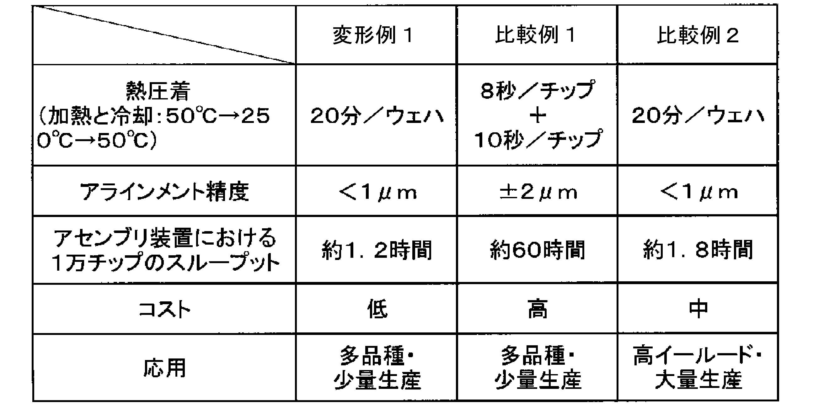
(変形例2)
(変形例3)
(変形例4)
Claims (22)
- 基板上に形成されチップを吸着する親液性領域と、
前記基板上であって前記親液性領域内に形成され、前記チップに静電力を発生させる電極と、
を備えた、チップ支持基板。 - 前記親液性領域は、複数の前記チップをそれぞれ吸着する複数の前記親液性領域を含み、
前記電極は、前記複数の親液性領域それぞれ内に形成されていることを特徴とする請求項1記載のチップ支持基板。 - 前記基板は、半導体、ガラス、セラミック、プラスチック、インターポーザ基板の何れかでなる、請求項1または2に記載のチップ支持基板。
- 前記複数の親液性領域は、絶縁膜から形成されている、請求項1から3のいずれか一項記載のチップ支持基板。
- 前記基板上の前記親液性領域が配置されていない領域は、前記親液性領域より親液性が低い領域からなる、請求項1から4のいずれか一項記載のチップ支持基板。
- 前記電極は、前記親液性領域内に形成された陰極と陽極とを含む、請求項1から5のいずれか一項記載のチップ支持基板。
- 前記親液性領域内において、前記陰極と前記陽極とは、前記基板の上面に平行な第1方向と前記上面に平行であり第1方向に交差する第2方向とに格子状に配列されている、請求項6記載のチップ支持基板。
- 前記電極のうち、前記陽極と前記陰極と、の配置を任意に設定可能である、請求項6または7記載のチップ支持基板。
- 請求項1から8のいずれか一項記載のチップ支持基板と、
前記親液性領域に積層されたチップと、
前記チップ上に積層された1層以上の別のチップと、
を含む、三次元集積回路。 - 前記チップは、上面に前記別のチップを吸着する別の親液性領域と前記チップの上面であって前記別の親液性領域内に形成され、前記別のチップに静電力を発生させる別の電極を有する、請求項9記載の三次元集積回路。
- 基板上に形成された親液性領域と、前記基板上であって前記親液性領域内に形成された電極と、を備えるチップ支持基板の前記親液性領域上に液体を介しチップを配置する工程と、
前記電極に電圧を印加することにより前記電極に対応するチップに静電力を発生させる工程と、
を含む、チップ支持方法。 - 前記親液性領域は、複数の前記チップをそれぞれ吸着する複数の前記親液性領域を含み、
前記電極は、前記複数の親液性領域それぞれ内に形成されており、
前記チップを配置する工程は、前記複数の親液性領域上にそれぞれ液体を介し前記複数のチップを配置する工程を含む、請求項11記載のチップ支持方法。 - 前記チップを前記親液性領域に吸着させる工程を含む請求項11または12記載のチップ支持方法。
- 前記電極は、前記親液性領域内に形成された陰極と陽極とを含み、
前記静電力を発生させる工程は、前記液体が存在する状態で前記陰極と前記陽極とに電圧を供給することにより、前記チップの中心が前記陰極と前記陽極との間に配置するように前記静電力を発生させる工程含む、請求項11から13のいずれか一項記載のチップ支持方法。 - 前記静電力を発生させる工程は、前記チップが前記チップ支持基板に吸着するように前記静電力を発生させる工程を含む、請求項10から13のいずれか一項記載のチップ支持方法。
- 前記チップが前記チップ支持基板に吸着された状態で、前記チップ上に別のチップを積層する工程を含む、請求項11から15のいずれか一項記載のチップ支持方法。
- 前記チップ支持基板に吸着された前記チップを別の基板にトランスファーする工程と、
前記別の基板にトランスファーされた前記チップを半導体ウェハにトランスファーする工程と、
を含む請求項11から15のいずれか一項記載のチップ支持方法。 - 前記チップ支持基板に吸着された前記チップを半導体ウェハ上にトランスファーする工程を含む請求項11から15のいずれか一項記載のチップ支持方法。
- 前記基板上の前記親液性領域が配置されていない領域は、前記親液性領域より親液性が低い領域からなる、請求項11から18のいずれか一項記載のチップ支持方法。
- 前記親液性の低い流域を除去する工程を含む、請求項19記載のチップ支持方法。
- 請求項11から20のいずれか一項記載のチップ支持方法を含む、三次元集積回路の製造方法。
- 基板上に形成された親液性領域と、前記基板上であって前記親液性領域内に形成された電極と、を備えるチップ支持基板を搭載するステージと、
前記親液性領域上に液滴を供給する液滴供給部と、
前記親液性領域上に供給された液滴上にチップを供給する搬送ロボットと、
前記電極に、前記チップに静電力が発生するように電圧を供給する電源部と、
を具備するアセンブリ装置。
Priority Applications (3)
| Application Number | Priority Date | Filing Date | Title |
|---|---|---|---|
| US14/427,232 US9449948B2 (en) | 2012-09-23 | 2013-09-13 | Chip support substrate, chip support method, three-dimensional integrated circuit, assembly device, and fabrication method of three-dimensional integrated circuit |
| KR1020157006841A KR101681437B1 (ko) | 2012-09-23 | 2013-09-13 | 칩 지지 기판, 칩 지지 방법, 3차원 집적 회로, 어셈블리 장치 및 3차원 집적 회로의 제조 방법 |
| JP2014536837A JP5963374B2 (ja) | 2012-09-23 | 2013-09-13 | チップ支持基板、チップ支持方法、三次元集積回路、アセンブリ装置及び三次元集積回路の製造方法 |
Applications Claiming Priority (2)
| Application Number | Priority Date | Filing Date | Title |
|---|---|---|---|
| JP2012209003 | 2012-09-23 | ||
| JP2012-209003 | 2012-09-23 |
Publications (1)
| Publication Number | Publication Date |
|---|---|
| WO2014046052A1 true WO2014046052A1 (ja) | 2014-03-27 |
Family
ID=50341365
Family Applications (1)
| Application Number | Title | Priority Date | Filing Date |
|---|---|---|---|
| PCT/JP2013/074876 Ceased WO2014046052A1 (ja) | 2012-09-23 | 2013-09-13 | チップ支持基板、チップ支持方法、三次元集積回路、アセンブリ装置及び三次元集積回路の製造方法 |
Country Status (5)
| Country | Link |
|---|---|
| US (1) | US9449948B2 (ja) |
| JP (1) | JP5963374B2 (ja) |
| KR (1) | KR101681437B1 (ja) |
| TW (1) | TW201419457A (ja) |
| WO (1) | WO2014046052A1 (ja) |
Cited By (15)
| Publication number | Priority date | Publication date | Assignee | Title |
|---|---|---|---|---|
| KR20160000869A (ko) * | 2014-06-25 | 2016-01-05 | 타이완 세미콘덕터 매뉴팩쳐링 컴퍼니 리미티드 | 반도체 소자 및 그 제조 방법 |
| KR20160001912A (ko) * | 2014-06-27 | 2016-01-07 | 삼성전자주식회사 | 오버행을 극복할 수 있는 반도체 패키지 및 그 제조방법 |
| EP3221903A4 (en) * | 2015-07-14 | 2017-11-29 | Goertek Inc | Transferring method, manufacturing method, device and electronic apparatus of micro-led |
| JP2017535967A (ja) * | 2015-07-14 | 2017-11-30 | ゴルテック.インク | フリップダイの組立方法、製造方法、装置及び電子機器 |
| JP2018056452A (ja) * | 2016-09-30 | 2018-04-05 | 株式会社ディスコ | 搬送トレイ、及び搬送トレイの給電装置 |
| JP2019096740A (ja) * | 2017-11-22 | 2019-06-20 | 富士通株式会社 | 電子装置 |
| US20210090954A1 (en) * | 2019-09-19 | 2021-03-25 | Disco Corporation | Method of processing wafer, and chip measuring apparatus |
| CN112992757A (zh) * | 2020-07-03 | 2021-06-18 | 重庆康佳光电技术研究院有限公司 | 微发光二极管芯片巨量转移方法 |
| JP2021516453A (ja) * | 2017-12-22 | 2021-07-01 | ボード オブ リージェンツ, ザ ユニバーシティ オブ テキサス システムBoard Of Regents, The University Of Texas System | ナノスケール整列3次元積層集積回路 |
| JP2021535613A (ja) * | 2018-09-04 | 2021-12-16 | 中芯集成電路(寧波)有限公司 | ウェハレベルパッケージ方法及びパッケージ構造 |
| JPWO2022038745A1 (ja) * | 2020-08-20 | 2022-02-24 | ||
| JP2024518025A (ja) * | 2021-03-29 | 2024-04-24 | ボード オブ リージェンツ,ザ ユニバーシティ オブ テキサス システム | 触媒影響化学エッチングのためのプロセスおよび適用 |
| WO2024147278A1 (ja) * | 2023-01-06 | 2024-07-11 | ヤマハロボティクスホールディングス株式会社 | 半導体チップのアライメント方法、接合方法、半導体装置、並びに電子部品製造システム |
| WO2025142389A1 (ja) * | 2023-12-28 | 2025-07-03 | 東京エレクトロン株式会社 | 処理方法及び処理システム |
| WO2025197893A1 (ja) * | 2024-03-19 | 2025-09-25 | ボンドテック株式会社 | 接合方法および接合システム |
Families Citing this family (23)
| Publication number | Priority date | Publication date | Assignee | Title |
|---|---|---|---|---|
| US9105629B2 (en) | 2013-03-07 | 2015-08-11 | International Business Machines Corporation | Selective area heating for 3D chip stack |
| EP2889900B1 (en) * | 2013-12-19 | 2019-11-06 | IMEC vzw | Method for aligning micro-electronic components using an alignment liquid and electrostatic alignment as well as corresponding assembly of aligned micro-electronic components |
| JP6377936B2 (ja) * | 2014-04-01 | 2018-08-22 | エイブリック株式会社 | 半導体ウェハ |
| JP6467981B2 (ja) * | 2015-02-25 | 2019-02-13 | 株式会社デンソー | 半導体装置およびその製造方法 |
| CN105931997B (zh) * | 2015-02-27 | 2019-02-05 | 胡迪群 | 暂时性复合式载板 |
| TWI557831B (zh) * | 2015-05-15 | 2016-11-11 | 友達光電股份有限公司 | 微組件的傳送方法 |
| CN105470173B (zh) * | 2015-12-15 | 2018-08-14 | 上海微电子装备(集团)股份有限公司 | 一种芯片接合系统及方法 |
| WO2018157937A1 (de) * | 2017-03-02 | 2018-09-07 | Ev Group E. Thallner Gmbh | Verfahren und vorrichtung zum bonden von chips |
| FR3063832B1 (fr) * | 2017-03-08 | 2019-03-22 | Commissariat A L'energie Atomique Et Aux Energies Alternatives | Procede d'auto-assemblage de composants microelectroniques |
| KR102115188B1 (ko) * | 2018-06-22 | 2020-05-26 | 엘지전자 주식회사 | 반도체 발광소자를 이용한 디스플레이 장치 |
| WO2020040605A1 (ko) * | 2018-08-23 | 2020-02-27 | 엘지디스플레이 주식회사 | 마이크로 칩 전사 장치용 이송 헤드 및 이를 갖는 마이크로 칩 전사 장치와 그 전사 방법 |
| SG11202102246WA (en) | 2018-09-06 | 2021-04-29 | Univ Texas | Nanofabrication and design techniques for 3d ics and configurable asics |
| KR102260638B1 (ko) * | 2019-09-26 | 2021-06-04 | 엘지전자 주식회사 | 반도체 발광소자의 자가조립 장치 |
| KR102323256B1 (ko) | 2019-09-19 | 2021-11-08 | 엘지전자 주식회사 | 반도체 발광소자의 자가조립 장치 |
| WO2021054508A1 (ko) | 2019-09-19 | 2021-03-25 | 엘지전자 주식회사 | 반도체 발광소자의 자가조립 장치 |
| WO2021054548A1 (en) * | 2019-09-19 | 2021-03-25 | Lg Electronics Inc. | Substrate chuck for self-assembling semiconductor light-emitting diodes |
| WO2021054550A1 (en) | 2019-09-19 | 2021-03-25 | Lg Electronics Inc. | Device for self-assembling semiconductor light-emitting diodes |
| WO2020117032A2 (ko) * | 2019-09-19 | 2020-06-11 | 엘지전자 주식회사 | 반도체 발광소자의 자가조립용 기판 척 |
| WO2021054507A1 (ko) | 2019-09-19 | 2021-03-25 | 엘지전자 주식회사 | 반도체 발광소자의 자가조립 장치 |
| CN110752145B (zh) * | 2019-10-28 | 2022-03-01 | 清华大学 | 基于液体毛细力和表面张力的转印方法和转印头 |
| WO2022172349A1 (ja) * | 2021-02-10 | 2022-08-18 | キヤノンアネルバ株式会社 | 化学結合法及びパッケージ型電子部品 |
| CN115706135A (zh) * | 2021-08-17 | 2023-02-17 | 群创光电股份有限公司 | 电子装置的制造方法 |
| US12417998B2 (en) * | 2022-02-11 | 2025-09-16 | Applied Materials, Inc. | Procedure to enable die rework for hybrid bonding |
Citations (4)
| Publication number | Priority date | Publication date | Assignee | Title |
|---|---|---|---|---|
| JP2008177215A (ja) * | 2007-01-16 | 2008-07-31 | Sharp Corp | 基板貼り合わせ方法および基板貼り合わせ装置 |
| JP2010153645A (ja) * | 2008-12-25 | 2010-07-08 | Nikon Corp | 積層半導体装置の製造方法 |
| JP2010206021A (ja) * | 2009-03-04 | 2010-09-16 | Panasonic Corp | 電子部品実装構造体、およびその製造方法 |
| JP2011192663A (ja) * | 2010-03-11 | 2011-09-29 | Tokyo Electron Ltd | 実装方法及び実装装置 |
Family Cites Families (8)
| Publication number | Priority date | Publication date | Assignee | Title |
|---|---|---|---|---|
| US5868305A (en) * | 1995-09-25 | 1999-02-09 | Mpm Corporation | Jet soldering system and method |
| JP3719909B2 (ja) | 2000-05-24 | 2005-11-24 | 洋太郎 畑村 | 部品の製造方法 |
| JP2003158150A (ja) * | 2001-11-22 | 2003-05-30 | Sumitomo Osaka Cement Co Ltd | 半導体チップ実装装置 |
| EP1736035A4 (en) | 2004-03-29 | 2009-01-07 | Articulated Technologies Llc | FROM ROLE TO ROLLED LIGHT LEAF AND CAPSULE SEMICONDUCTOR CIRCUIT ELEMENTS |
| JP5007127B2 (ja) | 2004-12-28 | 2012-08-22 | 光正 小柳 | 自己組織化機能を用いた集積回路装置の製造方法及び製造装置 |
| US7943052B2 (en) * | 2005-07-05 | 2011-05-17 | National Taiwan University | Method for self-assembling microstructures |
| FR2929864B1 (fr) * | 2008-04-09 | 2020-02-07 | Commissariat A L'energie Atomique | Auto-assemblage de puces sur un substrat |
| US8586410B2 (en) * | 2010-01-25 | 2013-11-19 | University Of Florida Research Foundation, Inc. | Enhanced magnetic self-assembly using integrated micromagnets |
-
2013
- 2013-09-13 JP JP2014536837A patent/JP5963374B2/ja active Active
- 2013-09-13 WO PCT/JP2013/074876 patent/WO2014046052A1/ja not_active Ceased
- 2013-09-13 US US14/427,232 patent/US9449948B2/en active Active
- 2013-09-13 KR KR1020157006841A patent/KR101681437B1/ko active Active
- 2013-09-17 TW TW102133634A patent/TW201419457A/zh unknown
Patent Citations (4)
| Publication number | Priority date | Publication date | Assignee | Title |
|---|---|---|---|---|
| JP2008177215A (ja) * | 2007-01-16 | 2008-07-31 | Sharp Corp | 基板貼り合わせ方法および基板貼り合わせ装置 |
| JP2010153645A (ja) * | 2008-12-25 | 2010-07-08 | Nikon Corp | 積層半導体装置の製造方法 |
| JP2010206021A (ja) * | 2009-03-04 | 2010-09-16 | Panasonic Corp | 電子部品実装構造体、およびその製造方法 |
| JP2011192663A (ja) * | 2010-03-11 | 2011-09-29 | Tokyo Electron Ltd | 実装方法及び実装装置 |
Cited By (37)
| Publication number | Priority date | Publication date | Assignee | Title |
|---|---|---|---|---|
| KR20160000869A (ko) * | 2014-06-25 | 2016-01-05 | 타이완 세미콘덕터 매뉴팩쳐링 컴퍼니 리미티드 | 반도체 소자 및 그 제조 방법 |
| KR101712271B1 (ko) | 2014-06-25 | 2017-03-13 | 타이완 세미콘덕터 매뉴팩쳐링 컴퍼니 리미티드 | 반도체 소자 및 그 제조 방법 |
| KR20160001912A (ko) * | 2014-06-27 | 2016-01-07 | 삼성전자주식회사 | 오버행을 극복할 수 있는 반도체 패키지 및 그 제조방법 |
| KR102245003B1 (ko) * | 2014-06-27 | 2021-04-28 | 삼성전자주식회사 | 오버행을 극복할 수 있는 반도체 패키지 및 그 제조방법 |
| EP3221903A4 (en) * | 2015-07-14 | 2017-11-29 | Goertek Inc | Transferring method, manufacturing method, device and electronic apparatus of micro-led |
| JP2017539097A (ja) * | 2015-07-14 | 2017-12-28 | ゴルテック.インク | マイクロ発光ダイオードの搬送方法、製造方法、マイクロ発光ダイオード装置、及び電子機器 |
| JP2017535967A (ja) * | 2015-07-14 | 2017-11-30 | ゴルテック.インク | フリップダイの組立方法、製造方法、装置及び電子機器 |
| JP2018056452A (ja) * | 2016-09-30 | 2018-04-05 | 株式会社ディスコ | 搬送トレイ、及び搬送トレイの給電装置 |
| JP2019096740A (ja) * | 2017-11-22 | 2019-06-20 | 富士通株式会社 | 電子装置 |
| JP7059585B2 (ja) | 2017-11-22 | 2022-04-26 | 富士通株式会社 | 電子装置 |
| US11600525B2 (en) | 2017-12-22 | 2023-03-07 | Board Of Regents, The University Of Texas System | Nanoscale-aligned three-dimensional stacked integrated circuit |
| JP2023082186A (ja) * | 2017-12-22 | 2023-06-13 | ボード オブ リージェンツ,ザ ユニバーシティ オブ テキサス システム | ナノスケール整列3次元積層集積回路 |
| JP2021516453A (ja) * | 2017-12-22 | 2021-07-01 | ボード オブ リージェンツ, ザ ユニバーシティ オブ テキサス システムBoard Of Regents, The University Of Texas System | ナノスケール整列3次元積層集積回路 |
| JP7704798B2 (ja) | 2017-12-22 | 2025-07-08 | ボード オブ リージェンツ,ザ ユニバーシティ オブ テキサス システム | ナノスケール整列3次元積層集積回路 |
| US12094775B2 (en) | 2017-12-22 | 2024-09-17 | Board Of Regents, The University Of Texas System | Nanoscale-aligned three-dimensional stacked integrated circuit |
| US11450582B2 (en) | 2018-09-04 | 2022-09-20 | Ningbo Semiconductor International Corporation | Wafer-level package structure |
| JP2021535613A (ja) * | 2018-09-04 | 2021-12-16 | 中芯集成電路(寧波)有限公司 | ウェハレベルパッケージ方法及びパッケージ構造 |
| US11901234B2 (en) | 2019-09-19 | 2024-02-13 | Disco Corporation | Method of processing wafer, and chip measuring apparatus |
| US20210090954A1 (en) * | 2019-09-19 | 2021-03-25 | Disco Corporation | Method of processing wafer, and chip measuring apparatus |
| US11637039B2 (en) * | 2019-09-19 | 2023-04-25 | Disco Corporation | Method of processing wafer, and chip measuring apparatus |
| CN112992757B (zh) * | 2020-07-03 | 2022-04-29 | 重庆康佳光电技术研究院有限公司 | 微发光二极管芯片巨量转移方法 |
| CN112992757A (zh) * | 2020-07-03 | 2021-06-18 | 重庆康佳光电技术研究院有限公司 | 微发光二极管芯片巨量转移方法 |
| JP7133254B2 (ja) | 2020-08-20 | 2022-09-08 | 株式会社新川 | 配置装置及び配置方法 |
| JPWO2022038745A1 (ja) * | 2020-08-20 | 2022-02-24 | ||
| KR102442373B1 (ko) | 2020-08-20 | 2022-09-14 | 가부시키가이샤 신가와 | 배치 장치 및 배치 방법 |
| KR20220023747A (ko) * | 2020-08-20 | 2022-03-02 | 가부시키가이샤 신가와 | 배치 장치 및 배치 방법 |
| TWI782664B (zh) * | 2020-08-20 | 2022-11-01 | 日商新川股份有限公司 | 配置裝置及配置方法 |
| US12112962B2 (en) | 2020-08-20 | 2024-10-08 | Shinkawa Ltd. | Arrangement apparatus and arrangement method |
| WO2022038745A1 (ja) * | 2020-08-20 | 2022-02-24 | 株式会社新川 | 配置装置及び配置方法 |
| JP2024518025A (ja) * | 2021-03-29 | 2024-04-24 | ボード オブ リージェンツ,ザ ユニバーシティ オブ テキサス システム | 触媒影響化学エッチングのためのプロセスおよび適用 |
| JP2024097401A (ja) * | 2023-01-06 | 2024-07-19 | ヤマハロボティクスホールディングス株式会社 | 半導体チップのアライメント方法、接合方法、半導体装置、並びに電子部品製造システム |
| WO2024147278A1 (ja) * | 2023-01-06 | 2024-07-11 | ヤマハロボティクスホールディングス株式会社 | 半導体チップのアライメント方法、接合方法、半導体装置、並びに電子部品製造システム |
| JP7883723B2 (ja) | 2023-01-06 | 2026-07-02 | ヤマハロボティクス株式会社 | 半導体チップのアライメント方法、接合方法、半導体装置、並びに電子部品製造システム |
| WO2025142389A1 (ja) * | 2023-12-28 | 2025-07-03 | 東京エレクトロン株式会社 | 処理方法及び処理システム |
| WO2025197893A1 (ja) * | 2024-03-19 | 2025-09-25 | ボンドテック株式会社 | 接合方法および接合システム |
| JPWO2025197893A1 (ja) * | 2024-03-19 | 2025-09-25 | ||
| JP7874924B2 (ja) | 2024-03-19 | 2026-06-17 | ボンドテック株式会社 | 接合方法および接合システム |
Also Published As
| Publication number | Publication date |
|---|---|
| KR101681437B1 (ko) | 2016-11-30 |
| KR20150046162A (ko) | 2015-04-29 |
| TW201419457A (zh) | 2014-05-16 |
| US9449948B2 (en) | 2016-09-20 |
| JP5963374B2 (ja) | 2016-08-03 |
| US20150228622A1 (en) | 2015-08-13 |
| JPWO2014046052A1 (ja) | 2016-08-18 |
Similar Documents
| Publication | Publication Date | Title |
|---|---|---|
| JP5963374B2 (ja) | チップ支持基板、チップ支持方法、三次元集積回路、アセンブリ装置及び三次元集積回路の製造方法 | |
| US8283208B2 (en) | Method and apparatus for fabricating integrated circuit device using self-organizing function | |
| CN101937853B (zh) | 集成电路结构的形成方法 | |
| US7833895B2 (en) | TSVS having chemically exposed TSV tips for integrated circuit devices | |
| US9984943B2 (en) | Systems and methods for aligning and coupling semiconductor structures | |
| US20180053730A1 (en) | Semiconductor Packages and Methods of Forming the Same | |
| US8456004B2 (en) | Template wafer and process for small pitch flip-chip interconnect hybridization | |
| Fukushima et al. | Reconfigured-wafer-to-wafer 3-D integration using parallel self-assembly of chips with Cu–SnAg microbumps and a nonconductive film | |
| Fukushima et al. | Multichip self-assembly technology for advanced die-to-wafer 3-D integration to precisely align known good dies in batch processing | |
| CN114664782A (zh) | 用于具有直接键合的微电子组件的载体 | |
| Hashiguchi et al. | Self-assembly and electrostatic carrier technology for via-last TSV formation using transfer stacking-based chip-to-wafer 3-D integration | |
| US20250105009A1 (en) | High-precision heterogeneous integration | |
| US20260130172A1 (en) | Miniature Electrostatic Chuck for Die-to-Substrate Bonding and Method for Manufacturing the Same | |
| EP4020536A1 (en) | Carrier for microelectronic assemblies having texturized surface with microstructures | |
| Ito et al. | Direct multichip-to-wafer 3D integration technology using flip-chip self-assembly of NCF-covered known good dies | |
| Lee et al. | Development of bumpless stacking with bottom–up TSV fabrication | |
| Ito et al. | Flux-assisted self-assembly with microbump bonding for 3D heterogeneous integration | |
| Lee et al. | A cavity chip interconnection technology for thick MEMS chip integration in MEMS-LSI multichip module | |
| Hashiguchi et al. | Temporary spin-on glass bonding technologies for via-last/backside-via 3D integration using multichip self-assembly | |
| Fukushima et al. | 3D integration technologies using self-assembly and electrostatic temporary multichip bonding | |
| Zehua et al. | 16-layer 3D stacking based on self-assembly technology for HBM application | |
| CN118830075A (zh) | 高精度异构集成 | |
| CN121843533A (zh) | 一种转接板及其制备方法、处理器及其制备方法 | |
| Fukushima et al. | Self‐Assembly Based 3D and Heterointegration | |
| Peng | Wafer-level fine pitch Cu-Cu bonding for 3-D stacking of integrated circuits |
Legal Events
| Date | Code | Title | Description |
|---|---|---|---|
| 121 | Ep: the epo has been informed by wipo that ep was designated in this application |
Ref document number: 13839140 Country of ref document: EP Kind code of ref document: A1 |
|
| ENP | Entry into the national phase |
Ref document number: 2014536837 Country of ref document: JP Kind code of ref document: A |
|
| WWE | Wipo information: entry into national phase |
Ref document number: 14427232 Country of ref document: US |
|
| WWE | Wipo information: entry into national phase |
Ref document number: 1020157006841 Country of ref document: KR |
|
| NENP | Non-entry into the national phase |
Ref country code: DE |
|
| 122 | Ep: pct application non-entry in european phase |
Ref document number: 13839140 Country of ref document: EP Kind code of ref document: A1 |