WO2013179765A1 - 撮像装置の製造方法および半導体装置の製造方法 - Google Patents
撮像装置の製造方法および半導体装置の製造方法 Download PDFInfo
- Publication number
- WO2013179765A1 WO2013179765A1 PCT/JP2013/060343 JP2013060343W WO2013179765A1 WO 2013179765 A1 WO2013179765 A1 WO 2013179765A1 JP 2013060343 W JP2013060343 W JP 2013060343W WO 2013179765 A1 WO2013179765 A1 WO 2013179765A1
- Authority
- WO
- WIPO (PCT)
- Prior art keywords
- imaging
- manufacturing
- bonded
- wafer
- chip
- Prior art date
Links
- 238000003384 imaging method Methods 0.000 title claims abstract description 247
- 238000004519 manufacturing process Methods 0.000 title claims abstract description 78
- 239000004065 semiconductor Substances 0.000 title claims description 51
- 238000007789 sealing Methods 0.000 claims abstract description 71
- 239000000758 substrate Substances 0.000 claims abstract description 59
- 239000012790 adhesive layer Substances 0.000 claims abstract description 27
- 238000012545 processing Methods 0.000 claims abstract description 21
- 238000005520 cutting process Methods 0.000 claims abstract description 16
- 238000011049 filling Methods 0.000 claims abstract description 12
- 230000002950 deficient Effects 0.000 claims abstract description 10
- 238000007689 inspection Methods 0.000 claims abstract description 8
- 238000000034 method Methods 0.000 claims description 78
- 230000008569 process Effects 0.000 claims description 39
- 238000000059 patterning Methods 0.000 claims description 5
- 239000011521 glass Substances 0.000 abstract description 68
- 235000012431 wafers Nutrition 0.000 description 107
- 239000000853 adhesive Substances 0.000 description 43
- 230000001070 adhesive effect Effects 0.000 description 43
- 229920005989 resin Polymers 0.000 description 37
- 239000011347 resin Substances 0.000 description 37
- 230000004048 modification Effects 0.000 description 31
- 238000012986 modification Methods 0.000 description 31
- 238000005530 etching Methods 0.000 description 14
- 238000001723 curing Methods 0.000 description 10
- 239000006059 cover glass Substances 0.000 description 8
- 230000002093 peripheral effect Effects 0.000 description 8
- XUIMIQQOPSSXEZ-UHFFFAOYSA-N Silicon Chemical compound [Si] XUIMIQQOPSSXEZ-UHFFFAOYSA-N 0.000 description 7
- 238000011156 evaluation Methods 0.000 description 7
- 239000010703 silicon Substances 0.000 description 7
- 229910052710 silicon Inorganic materials 0.000 description 7
- 230000015572 biosynthetic process Effects 0.000 description 6
- 238000000227 grinding Methods 0.000 description 6
- 239000007788 liquid Substances 0.000 description 6
- 230000000694 effects Effects 0.000 description 5
- 239000010410 layer Substances 0.000 description 5
- 239000000463 material Substances 0.000 description 5
- 238000000926 separation method Methods 0.000 description 4
- 238000003848 UV Light-Curing Methods 0.000 description 3
- VYPSYNLAJGMNEJ-UHFFFAOYSA-N Silicium dioxide Chemical compound O=[Si]=O VYPSYNLAJGMNEJ-UHFFFAOYSA-N 0.000 description 2
- 230000007547 defect Effects 0.000 description 2
- 238000010438 heat treatment Methods 0.000 description 2
- 238000005286 illumination Methods 0.000 description 2
- 238000000206 photolithography Methods 0.000 description 2
- 239000000049 pigment Substances 0.000 description 2
- 230000001681 protective effect Effects 0.000 description 2
- 239000000126 substance Substances 0.000 description 2
- WGTYBPLFGIVFAS-UHFFFAOYSA-M tetramethylammonium hydroxide Chemical compound [OH-].C[N+](C)(C)C WGTYBPLFGIVFAS-UHFFFAOYSA-M 0.000 description 2
- 238000001029 thermal curing Methods 0.000 description 2
- 239000004642 Polyimide Substances 0.000 description 1
- 229910052581 Si3N4 Inorganic materials 0.000 description 1
- 239000006061 abrasive grain Substances 0.000 description 1
- 230000009471 action Effects 0.000 description 1
- 239000012670 alkaline solution Substances 0.000 description 1
- UMIVXZPTRXBADB-UHFFFAOYSA-N benzocyclobutene Chemical compound C1=CC=C2CCC2=C1 UMIVXZPTRXBADB-UHFFFAOYSA-N 0.000 description 1
- 239000005388 borosilicate glass Substances 0.000 description 1
- 239000002775 capsule Substances 0.000 description 1
- 238000000576 coating method Methods 0.000 description 1
- 239000004020 conductor Substances 0.000 description 1
- 238000001816 cooling Methods 0.000 description 1
- 238000005336 cracking Methods 0.000 description 1
- 239000013078 crystal Substances 0.000 description 1
- 230000007812 deficiency Effects 0.000 description 1
- 230000032798 delamination Effects 0.000 description 1
- 239000010432 diamond Substances 0.000 description 1
- 229910003460 diamond Inorganic materials 0.000 description 1
- 238000001312 dry etching Methods 0.000 description 1
- 238000010292 electrical insulation Methods 0.000 description 1
- 239000003822 epoxy resin Substances 0.000 description 1
- 238000005429 filling process Methods 0.000 description 1
- 238000007731 hot pressing Methods 0.000 description 1
- 239000011810 insulating material Substances 0.000 description 1
- 239000012212 insulator Substances 0.000 description 1
- 238000005304 joining Methods 0.000 description 1
- 238000010030 laminating Methods 0.000 description 1
- 238000003475 lamination Methods 0.000 description 1
- 239000002184 metal Substances 0.000 description 1
- 239000000203 mixture Substances 0.000 description 1
- 238000013008 moisture curing Methods 0.000 description 1
- 230000035699 permeability Effects 0.000 description 1
- 229920002120 photoresistant polymer Polymers 0.000 description 1
- 238000005268 plasma chemical vapour deposition Methods 0.000 description 1
- 238000007747 plating Methods 0.000 description 1
- 238000005498 polishing Methods 0.000 description 1
- 238000007517 polishing process Methods 0.000 description 1
- 229920000647 polyepoxide Polymers 0.000 description 1
- 229920001721 polyimide Polymers 0.000 description 1
- 238000003825 pressing Methods 0.000 description 1
- 238000003672 processing method Methods 0.000 description 1
- 230000008707 rearrangement Effects 0.000 description 1
- 230000009467 reduction Effects 0.000 description 1
- 238000012958 reprocessing Methods 0.000 description 1
- 239000000523 sample Substances 0.000 description 1
- 229910052594 sapphire Inorganic materials 0.000 description 1
- 239000010980 sapphire Substances 0.000 description 1
- 230000035945 sensitivity Effects 0.000 description 1
- HQVNEWCFYHHQES-UHFFFAOYSA-N silicon nitride Chemical compound N12[Si]34N5[Si]62N3[Si]51N64 HQVNEWCFYHHQES-UHFFFAOYSA-N 0.000 description 1
- 229910052814 silicon oxide Inorganic materials 0.000 description 1
- 229920002050 silicone resin Polymers 0.000 description 1
- 229910000679 solder Inorganic materials 0.000 description 1
- 239000000243 solution Substances 0.000 description 1
- 239000002904 solvent Substances 0.000 description 1
- 238000004528 spin coating Methods 0.000 description 1
- 238000003892 spreading Methods 0.000 description 1
- 230000007480 spreading Effects 0.000 description 1
- 230000003746 surface roughness Effects 0.000 description 1
- 238000002834 transmittance Methods 0.000 description 1
- 238000009281 ultraviolet germicidal irradiation Methods 0.000 description 1
- 239000011800 void material Substances 0.000 description 1
- XLYOFNOQVPJJNP-UHFFFAOYSA-N water Substances O XLYOFNOQVPJJNP-UHFFFAOYSA-N 0.000 description 1
- 238000001039 wet etching Methods 0.000 description 1
Images


Classifications
-
- H—ELECTRICITY
- H01—ELECTRIC ELEMENTS
- H01L—SEMICONDUCTOR DEVICES NOT COVERED BY CLASS H10
- H01L27/00—Devices consisting of a plurality of semiconductor or other solid-state components formed in or on a common substrate
- H01L27/14—Devices consisting of a plurality of semiconductor or other solid-state components formed in or on a common substrate including semiconductor components sensitive to infrared radiation, light, electromagnetic radiation of shorter wavelength or corpuscular radiation and specially adapted either for the conversion of the energy of such radiation into electrical energy or for the control of electrical energy by such radiation
- H01L27/144—Devices controlled by radiation
- H01L27/146—Imager structures
- H01L27/14683—Processes or apparatus peculiar to the manufacture or treatment of these devices or parts thereof
- H01L27/14685—Process for coatings or optical elements
-
- H—ELECTRICITY
- H01—ELECTRIC ELEMENTS
- H01L—SEMICONDUCTOR DEVICES NOT COVERED BY CLASS H10
- H01L25/00—Assemblies consisting of a plurality of individual semiconductor or other solid state devices ; Multistep manufacturing processes thereof
- H01L25/03—Assemblies consisting of a plurality of individual semiconductor or other solid state devices ; Multistep manufacturing processes thereof all the devices being of a type provided for in the same subgroup of groups H01L27/00 - H01L33/00, or in a single subclass of H10K, H10N, e.g. assemblies of rectifier diodes
- H01L25/04—Assemblies consisting of a plurality of individual semiconductor or other solid state devices ; Multistep manufacturing processes thereof all the devices being of a type provided for in the same subgroup of groups H01L27/00 - H01L33/00, or in a single subclass of H10K, H10N, e.g. assemblies of rectifier diodes the devices not having separate containers
- H01L25/041—Assemblies consisting of a plurality of individual semiconductor or other solid state devices ; Multistep manufacturing processes thereof all the devices being of a type provided for in the same subgroup of groups H01L27/00 - H01L33/00, or in a single subclass of H10K, H10N, e.g. assemblies of rectifier diodes the devices not having separate containers the devices being of a type provided for in group H01L31/00
- H01L25/042—Assemblies consisting of a plurality of individual semiconductor or other solid state devices ; Multistep manufacturing processes thereof all the devices being of a type provided for in the same subgroup of groups H01L27/00 - H01L33/00, or in a single subclass of H10K, H10N, e.g. assemblies of rectifier diodes the devices not having separate containers the devices being of a type provided for in group H01L31/00 the devices being arranged next to each other
-
- H—ELECTRICITY
- H01—ELECTRIC ELEMENTS
- H01L—SEMICONDUCTOR DEVICES NOT COVERED BY CLASS H10
- H01L27/00—Devices consisting of a plurality of semiconductor or other solid-state components formed in or on a common substrate
- H01L27/14—Devices consisting of a plurality of semiconductor or other solid-state components formed in or on a common substrate including semiconductor components sensitive to infrared radiation, light, electromagnetic radiation of shorter wavelength or corpuscular radiation and specially adapted either for the conversion of the energy of such radiation into electrical energy or for the control of electrical energy by such radiation
- H01L27/144—Devices controlled by radiation
- H01L27/146—Imager structures
- H01L27/14601—Structural or functional details thereof
- H01L27/14618—Containers
-
- H—ELECTRICITY
- H01—ELECTRIC ELEMENTS
- H01L—SEMICONDUCTOR DEVICES NOT COVERED BY CLASS H10
- H01L27/00—Devices consisting of a plurality of semiconductor or other solid-state components formed in or on a common substrate
- H01L27/14—Devices consisting of a plurality of semiconductor or other solid-state components formed in or on a common substrate including semiconductor components sensitive to infrared radiation, light, electromagnetic radiation of shorter wavelength or corpuscular radiation and specially adapted either for the conversion of the energy of such radiation into electrical energy or for the control of electrical energy by such radiation
- H01L27/144—Devices controlled by radiation
- H01L27/146—Imager structures
- H01L27/14601—Structural or functional details thereof
- H01L27/14625—Optical elements or arrangements associated with the device
-
- H—ELECTRICITY
- H01—ELECTRIC ELEMENTS
- H01L—SEMICONDUCTOR DEVICES NOT COVERED BY CLASS H10
- H01L27/00—Devices consisting of a plurality of semiconductor or other solid-state components formed in or on a common substrate
- H01L27/14—Devices consisting of a plurality of semiconductor or other solid-state components formed in or on a common substrate including semiconductor components sensitive to infrared radiation, light, electromagnetic radiation of shorter wavelength or corpuscular radiation and specially adapted either for the conversion of the energy of such radiation into electrical energy or for the control of electrical energy by such radiation
- H01L27/144—Devices controlled by radiation
- H01L27/146—Imager structures
- H01L27/14683—Processes or apparatus peculiar to the manufacture or treatment of these devices or parts thereof
- H01L27/14687—Wafer level processing
-
- H—ELECTRICITY
- H01—ELECTRIC ELEMENTS
- H01L—SEMICONDUCTOR DEVICES NOT COVERED BY CLASS H10
- H01L27/00—Devices consisting of a plurality of semiconductor or other solid-state components formed in or on a common substrate
- H01L27/14—Devices consisting of a plurality of semiconductor or other solid-state components formed in or on a common substrate including semiconductor components sensitive to infrared radiation, light, electromagnetic radiation of shorter wavelength or corpuscular radiation and specially adapted either for the conversion of the energy of such radiation into electrical energy or for the control of electrical energy by such radiation
- H01L27/144—Devices controlled by radiation
- H01L27/146—Imager structures
- H01L27/14683—Processes or apparatus peculiar to the manufacture or treatment of these devices or parts thereof
- H01L27/1469—Assemblies, i.e. hybrid integration
-
- H—ELECTRICITY
- H01—ELECTRIC ELEMENTS
- H01L—SEMICONDUCTOR DEVICES NOT COVERED BY CLASS H10
- H01L27/00—Devices consisting of a plurality of semiconductor or other solid-state components formed in or on a common substrate
- H01L27/14—Devices consisting of a plurality of semiconductor or other solid-state components formed in or on a common substrate including semiconductor components sensitive to infrared radiation, light, electromagnetic radiation of shorter wavelength or corpuscular radiation and specially adapted either for the conversion of the energy of such radiation into electrical energy or for the control of electrical energy by such radiation
- H01L27/144—Devices controlled by radiation
- H01L27/146—Imager structures
- H01L27/14683—Processes or apparatus peculiar to the manufacture or treatment of these devices or parts thereof
- H01L27/14698—Post-treatment for the devices, e.g. annealing, impurity-gettering, shor-circuit elimination, recrystallisation
-
- H—ELECTRICITY
- H04—ELECTRIC COMMUNICATION TECHNIQUE
- H04N—PICTORIAL COMMUNICATION, e.g. TELEVISION
- H04N25/00—Circuitry of solid-state image sensors [SSIS]; Control thereof
-
- H—ELECTRICITY
- H01—ELECTRIC ELEMENTS
- H01L—SEMICONDUCTOR DEVICES NOT COVERED BY CLASS H10
- H01L23/00—Details of semiconductor or other solid state devices
- H01L23/28—Encapsulations, e.g. encapsulating layers, coatings, e.g. for protection
- H01L23/31—Encapsulations, e.g. encapsulating layers, coatings, e.g. for protection characterised by the arrangement or shape
- H01L23/3107—Encapsulations, e.g. encapsulating layers, coatings, e.g. for protection characterised by the arrangement or shape the device being completely enclosed
- H01L23/3121—Encapsulations, e.g. encapsulating layers, coatings, e.g. for protection characterised by the arrangement or shape the device being completely enclosed a substrate forming part of the encapsulation
-
- H—ELECTRICITY
- H01—ELECTRIC ELEMENTS
- H01L—SEMICONDUCTOR DEVICES NOT COVERED BY CLASS H10
- H01L27/00—Devices consisting of a plurality of semiconductor or other solid-state components formed in or on a common substrate
- H01L27/14—Devices consisting of a plurality of semiconductor or other solid-state components formed in or on a common substrate including semiconductor components sensitive to infrared radiation, light, electromagnetic radiation of shorter wavelength or corpuscular radiation and specially adapted either for the conversion of the energy of such radiation into electrical energy or for the control of electrical energy by such radiation
- H01L27/144—Devices controlled by radiation
- H01L27/146—Imager structures
- H01L27/14601—Structural or functional details thereof
- H01L27/14625—Optical elements or arrangements associated with the device
- H01L27/14627—Microlenses
-
- H—ELECTRICITY
- H01—ELECTRIC ELEMENTS
- H01L—SEMICONDUCTOR DEVICES NOT COVERED BY CLASS H10
- H01L2924/00—Indexing scheme for arrangements or methods for connecting or disconnecting semiconductor or solid-state bodies as covered by H01L24/00
- H01L2924/0001—Technical content checked by a classifier
- H01L2924/0002—Not covered by any one of groups H01L24/00, H01L24/00 and H01L2224/00
Definitions
- the present invention relates to an imaging device manufacturing method and a semiconductor device manufacturing method including a step of cutting a bonded wafer in which a plurality of imaging chips (semiconductor chips) are bonded to a support substrate.
- a chip size package (CSP) method is used.
- CSP chip size package
- a through wiring reaching the second main surface is formed in a semiconductor chip having a semiconductor circuit portion formed on the first main surface, and an external connection terminal on the second main surface is connected to the wiring board.
- a transparent support member that protects the light receiving unit is joined to the first main surface of the imaging chip on which the light receiving unit that is a semiconductor circuit unit is formed.
- a wafer level chip size package (WL-CSP) method is used to collectively manufacture a plurality of imaging devices.
- WL-CSP method after processing such as through wiring formation is performed in a bonded wafer state in which an imaging chip substrate on which a plurality of light receiving portions are formed and a transparent support substrate are bonded via an adhesive layer, individual imaging is performed. Divided into devices.
- the imaging chip with the defective light receiving portion is also processed as an imaging device, and thus the manufacturing cost increases. Further, as the diameter of the semiconductor wafer is increased, all the processing facilities are required to cope with the large diameter, and the capital investment cost increases and the manufacturing cost increases, resulting in a decrease in productivity.
- a semiconductor chip mounted on a mounting surface of a silicon wafer is sealed with a sealing resin, and then the silicon wafer is polished from the surface opposite to the mounting surface.
- a method of manufacturing a package component by the CSP method that separates into individual package components is disclosed.
- the semiconductor chip is not processed, and the silicon wafer is processed to be an interposer of the semiconductor chip.
- Embodiments of the present invention are intended to provide a method for manufacturing an imaging device with high productivity and a method for manufacturing a semiconductor device with high productivity.
- a plurality of light receiving portions are formed on the first main surface, and an image pickup chip substrate on which an electrode pad is formed around each light receiving portion is cut to obtain a plurality of images.
- a step of manufacturing a chip and the first main surface of the imaging chip determined to be non-defective by inspection are transparent with a size or shape different from that of the imaging chip substrate via a transparent adhesive layer.
- a bonding process including: a process of thinning a bonding wafer to flatten a processing surface; a process of forming a through-wiring connected to the electrode pad; and the electrode pad via the through-wiring.
- Connected external Comprising a step of forming a connection electrode on the second major surface, and a step of cutting into pieces the bonding wafer, a.
- FIG. 11 is a plan view for explaining a method for manufacturing an imaging device according to Modification 2.
- 12 is a plan view for explaining a method for manufacturing the imaging device according to Modification 3.
- FIG. 10 is a plan view for explaining a method for manufacturing an imaging device according to Modification 4.
- FIG. 10 is a cross-sectional view for describing a method for manufacturing an imaging device according to Modification 5.
- FIG. 10 is a cross-sectional view for describing a method for manufacturing an imaging device according to Modification 5.
- FIG. 10 is a cross-sectional view for describing a method for manufacturing an imaging device according to Modification 5.
- FIG. 10 is a cross-sectional view for describing a method for manufacturing an imaging device according to Modification 5.
- FIG. 10 is a cross-sectional view for describing a method for manufacturing an imaging device according to Modification 5.
- FIG. 10 is a cross-sectional view for describing a method for manufacturing an imaging device according to Modification 5.
- FIG. 10 is a cross-sectional view for describing a method for manufacturing an imaging device according to Modification 6.
- FIG. 10 is a cross-sectional view for describing a method for manufacturing an imaging device according to Modification 6.
- FIG. 10 is a cross-sectional view for describing a method for manufacturing an imaging device according to Modification 6.
- FIG. 10 is a cross-sectional view for describing a method for manufacturing an imaging device
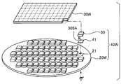
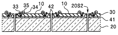
- an imaging device 10 that is a semiconductor device includes an imaging chip (imager chip) 30 and a cover glass 20 that is a support substrate portion (transparent flat plate portion) through an adhesive layer 41 made of a transparent resin. Are glued together.
- a light receiving portion 31 that is a semiconductor circuit portion is formed on the first main surface 30SA of the imaging chip 30. Further, around the light receiving portion 31 on the first main surface 30SA, a light receiving portion 31 and a wiring ( A plurality of electrode pads 32 connected by (not shown) are formed. The electrode pad 32 is connected to the external connection electrode 34 and the external connection terminal 35 of the second main surface 30SB through the through wiring 33.
- the plurality of electrode pads 32 supply power to the light receiving unit 31 and transmit / receive input / output signals to / from the light receiving unit 31. Further, the outer peripheral portion of the imaging chip 30 and the outer peripheral portion of the adhesive layer 41 are covered with a sealing member 42 without a gap.
- the planar view size of the cover glass 20 is larger than the planar view size of the imaging chip 30.
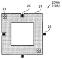
- an alignment mark 21 for arranging each imaging chip 30 at a predetermined position is formed on the glass wafer 20W. That is, since the glass wafer 20W is transparent, the alignment mark (first alignment mark) 21 and the alignment mark (second alignment mark) 36 of the imaging chip 30 are formed from the opposite surface of the alignment mark 21 formation surface (see FIG. 5)).
- an alignment mark 21 for placing the imaging chip 30 at a predetermined position is formed on a glass wafer 20W that is a transparent support substrate.
- the image pickup chip arrangement region 30 ⁇ / b> S is indicated by a broken line for explanation.
- the glass wafer 20W that is cut and becomes the cover glass 20 only needs to be transparent in the wavelength band of the light to be imaged.
- borosilicate glass, quartz glass, single crystal sapphire, or the like is used.
- the alignment mark 22 and the alignment mark 23 are formed simultaneously with the formation of the alignment mark 21.
- the alignment mark 22 is for dicing at the time of separation, and the alignment mark 23 is for processing such as formation of the through wiring 33 of the imaging chip 30.
- the alignment marks 21 and the like are formed, for example, by forming a metal layer made of Al or the like on the entire surface and then patterning by photolithography. For accurate positioning, it is preferable that there are two alignment marks for one positioning process.
- the alignment mark 21 and the like may be formed by partially etching the glass wafer 20W.
- Imaging Chip Manufacturing Process A plurality of light receiving portions 31 that are a plurality of semiconductor circuit portions and the respective light receiving portions 31 are connected to the first main surface 30SA of a semiconductor wafer such as a silicon wafer by a known semiconductor process.
- the imaging chip substrate 30W (see FIG. 2) is manufactured.
- the imaging chip substrate (semiconductor chip substrate) 30W is cut to produce a plurality of imaging chips (semiconductor chips) 30 shown in FIG.
- the sizes of the imaging chip substrate and the glass wafer 20W are selected in accordance with the available manufacturing equipment and the like according to the configuration and specifications of the imaging device to be manufactured.
- the imaging chip substrate and the glass wafer 20W can be different sizes. For example, even if the imaging chip is formed of a large-diameter 12 inch (300 mm) ⁇ or a larger substrate, the individual imaging chips 30 separated into individual pieces are re-applied to an 8-inch (200 mm) ⁇ glass wafer 20W. By performing processing by arranging (bonding), it is possible to manufacture with equipment for 8 inches (200 mm) ⁇ without using equipment for large-diameter wafers.
- substrates and wafers having different shapes such as an 8-inch (200 mm) ⁇ imaging chip substrate and a 6-inch (150 mm) square glass wafer 20W may be used depending on the equipment and apparatus.
- the imaging chip substrate and the glass wafer 20W having a size or shape suitable for usable manufacturing equipment can be used, the existing equipment can be used effectively.
- An imaging device can be manufactured.
- the imaging chip 30 determined as a non-defective product in the inspection process is used. That is, since a “defective chip” that is not a non-defective product is not used in the subsequent processes, even when the yield of the imaging chip 30 on the imaging chip substrate 30W is low, imaging obtained by rearrangement and reprocessing is performed. There is no reduction in chip yield.
- the inspection for determining the quality of the imaging chip may be performed for each imaging chip 30 in a state of being separated, but it is preferable to perform the inspection in the state of the imaging chip substrate 30W in terms of work efficiency.
- the alignment mark 36 corresponds to the alignment mark 21 on the glass wafer 20W. As shown in FIG. 5, the alignment marks 36 are preferably formed on the outer peripheral portions facing each other across the center of the imaging chip 30. By forming alignment marks on the glass wafer 20W and the imaging chip 30, respectively, the imaging chip 30 can be automatically mounted with high accuracy using a mounting apparatus.
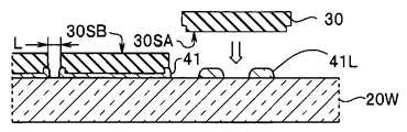
- a step portion 37 is formed on the outer peripheral portion of the first main surface 30SA of the imaging chip 30.
- the step portion 37 is manufactured by dicing the imaging chip substrate 30W by step cut.
- the imaging chip 30 having the stepped portion 37 can reduce the distance L between adjacent chips in order to prevent the adhesive 41L from spreading (fillet) to the outside of the imaging chip 30 when bonded to the glass wafer 20W.
- a microlens group may be disposed on the light receiving unit 31.
- Step S12> Bonding Step As shown in FIG. 6A, the plurality of imaging chips 30 are bonded to the glass wafer 20W by a predetermined distance L to produce a bonded wafer 40W. That is, a plurality of imaging chips 30 formed on the imaging chip substrate 30W under a predetermined arrangement condition are rearranged on the glass wafer 20W after cutting.
- the interval L needs to be longer than the thickness of the dicing blade used in the dicing process described later.
- the distance L is preferably 15 ⁇ m or more and 500 ⁇ m or less, which is slightly longer than the thickness of the dicing blade.
- interval L constant among all the imaging chips 30, it is possible to improve the workability in the sealing member filling step described later, and it is possible to uniformly fill the sealing member. Cracks due to uneven stress can be prevented.
- an appropriate amount of the liquid adhesive 41L is applied to five locations in the imaging chip arrangement region 30S of the glass wafer 20W.
- the imaging chip arrangement region 30S can be grasped by the two alignment marks 21 arranged on the diagonal line.
- a coating method for example, a dispensing method in which a solution is pushed out from a tip nozzle of a dispenser and applied is used.
- the adhesive 41L is highly transparent (for example, a transmittance at 90% or more at a visible wavelength), has a strong adhesive force, and does not deteriorate due to heat or the like in a subsequent process.
- BCB benzocyclobutene
- Resin epoxy resin, or silicone resin is used.
- the first alignment mark 21 of the glass wafer 20W and the second alignment mark 36 of the first main surface 30SA of the imaging chip 30 are aligned, The imaging chip 30 is bonded to the glass wafer 20W.
- the first alignment mark 21 and the second alignment mark 36 are set so as to be easily aligned.
- the first alignment mark 21 has a cross shape as shown in FIG. 4, and the second alignment mark 36 has four rectangles as shown in FIG.
- the reference marks may be formed on the glass wafer 20W, and the imaging chips 30 may be arranged at a predetermined pitch based on the reference marks. By using such a method, the throughput can be increased. Further, in place of the second alignment mark 36, alignment may be performed using a pattern such as an electrode pad 32 formed on the imaging chip 30.
- the liquid adhesive 41 ⁇ / b> L is cured with the alignment mark aligned, and becomes the adhesive layer 41.
- the second main surface of the imaging chip is completely cured while being pressed with a predetermined pressure by the wafer-like pressing jig, the parallelism between the main surface of the imaging chip and the main surface of the glass wafer 20W increases.
- a thermal curing method, a UV curing method, a UV curing method + thermal curing method, a UV curing method + a moisture curing method, or a room temperature curing method may be used.
- a flip chip bonder provided with a curing means for the adhesive 41L such as a heating unit or a UV irradiation unit, the imaging chip 30 can be disposed at a predetermined position and the adhesive 41L can be cured at the same time.
- the adhesive 41L may be completely cured by a flip chip bonder, but care must be taken in the case of the adhesive 41L that is likely to cause voids due to rapid curing.
- the curing by the flip chip bonder is semi-curing to such an extent that the imaging chip 30 disposed at a predetermined position does not move and cause a positional shift, and the plurality of imaging chips 30 are disposed on the glass wafer 20W. After that, it is preferable to collectively cure the adhesive 41L to form the adhesive layer 41.
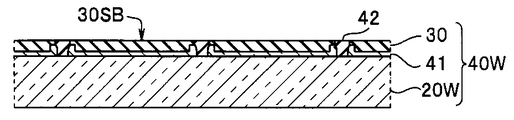
- a liquid sealing resin 42L filled by, for example, a dispensing method is provided between the plurality of imaging chips 30 disposed on the glass wafer 20W. Cured to form the sealing member 42. Instead of the dispensing method, the sealing resin 42L may be poured into the gap.
- the sealing member can be filled between the plurality of imaging chips 30 by capillary action.
- region where the vertex of the several imaging chip 30 opposes tends to become low in height (thickness), when the sealing resin 42L is filled. For this reason, after hardening sealing resin once, you may apply
- the sealing member 42 has a low moisture permeability for improving the moisture resistance of the imaging device 10 and is preferably not easily deteriorated by heat or plasma in a subsequent process.
- BCB resin or polyimide is used.
- the sealing member 42 may be the same as the adhesive layer 41 or may be a different material.
- the sealing member 42 has a function of a light shielding member for preventing external light from entering the light receiving portion.
- a light shielding material such as a dye or a black pigment.
- the sealing member 42 needs to be an insulator, when using a pigment etc., a nonelectroconductive material is used.
- the thickness of the sealing member 42 that is, the height to be filled only needs to be larger than the thickness of the imaging chip 30 after being thinned in step S14. That is, the sealing member 42 does not have to completely fill the space between the plurality of imaging chips 30 before the thinning process. Conversely, the sealing member 42 may protrude from the space between the imaging chips 30.
- the sealing member 42 is not limited to a hardened liquid resin.
- the sheet-like resin member may be cured after filling the space between the imaging chips 30 while embedding the imaging chip 30 by vacuum hot pressing or vacuum lamination.
- the second main surface 30SB side of the imaging chip 30 is flattened by reducing the thickness of the bonded wafer 40W. That is, a back grinding process and a CMP (Chemical Mechanical Polishing) process are performed from the second main surface 30SB side to flatten the processing surface.
- CMP Chemical Mechanical Polishing
- a diamond wheel called a back grinding wheel is used.
- the CMP process is performed to reduce the surface roughness of the surface ground by the back grinding process.
- the sealing member 42 that protrudes from between the imaging chips 30 is shaved with a blade.
- dishing in which the central portion of the surface of the sealing member 42 is concave may occur by the back grinding process and the CMP process. However, since the concave portion is removed in the dicing process, there is no problem.
- the second main surface 30SB of the imaging chip 30 and the surface of the sealing member 42 of the bonded wafer 40W after the thinning process form a flat surface.
- the bonded wafer 40W having a flattened surface can be processed in the same manner as a normal semiconductor wafer, unlike a wafer having irregularities on the surface.
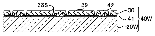
- the through via 33S for forming the through wiring 33 connected to the electrode pad 32 formed on the first main surface 30SA of the imaging chip 30 is a normal semiconductor wafer process. It is formed.
- an etching mask 39 having an opening in a region immediately above the electrode pad 32 is formed on the imaging chip 30 and the sealing member 42.
- the etching mask is also a protective film that protects the imaging chip 30 and the sealing member 42 from chemicals and plasma used in later processes.
- the etching mask 39 for example, a silicon oxide film or a silicon nitride film is used.
- plasma CVD is preferably used as a method for forming the etching mask 39.
- the alignment mark 23 for forming the through wiring formed on the glass wafer 20W is used for alignment of the photomask when forming a patterning mask (not shown) for forming an opening in the etching mask 39. .
- a through via 33S reaching the electrode pad 32 is formed by wet etching with an alkaline solution such as KOH or TMAH, or dry etching by an ICP-RIE method or the like.
- the through via 33S may be formed by a physical processing method such as laser processing.
- the through wiring 33 made of a conductor is formed inside the through via 33S.
- the external connection electrode 34 connected to the through wiring 33 is formed on the second main surface 30SB of the imaging chip 30, and the convex external connection terminal 35 is formed on the external connection electrode 34. Is disposed.
- a plating process may be used, and a solder ball or the like may be used for the external connection terminal 35.
- Step S15 Individualization process (dicing process) A large number of imaging devices 10 are manufactured from a single bonded wafer 40W by the separation process of cutting the bonded wafer 40W.
- the cutting is preferably a two-stage dicing method shown in FIGS. 6F and 6G. That is, after half-cutting the surface of the glass wafer 20W (upper side in the drawing) to about 10 to 200 ⁇ m and then performing full-cut dicing, the generation of cracks due to stress and peeling of the sealing member 42 can be prevented. . Further, in the two-stage dicing method, for the dicing of the sealing member 42, a blade type (bond material, abrasive grain size, concentration) suitable for the resin and processing conditions (feed speed, rotation speed) are used, and the glass wafer 20W is used.
- a blade type bond material, abrasive grain size, concentration
- the processing quality (resin burrs, glass chipping, resin layer delamination) can be improved.
- the resin blade may be made thicker than the glass blade, and a step cut may be formed in which a step is formed at the end of the imaging chip 30 after separation.
- the sealing member 42 on the dicing line may be removed by laser dicing or etching, and then the glass wafer 20W may be cut into full pieces by blade dicing or laser dicing for glass.
- Alignment marks 22 formed first on the glass wafer 20W are used for dicing alignment.
- a dicing alignment mark may be formed on the second main surface 30 SB of the imaging chip 30 or the sealing resin between the imaging chips 30 in a through wiring formation process or the like. .
- the bonded wafer 40W is manufactured using only the non-defective imaging chip 30. For this reason, since a defective chip does not become an imaging device, the imaging device 10 can be manufactured at low cost, and productivity is high.
- the manufacturing method of the embodiment it is possible to manufacture with the bonded wafer 40W having a predetermined diameter regardless of the diameter of the imaging chip substrate 30W.
- Productivity is high because processing equipment corresponding to large diameter is not required.
- the imaging chip since it is an imaging chip having a large thickness before processing that is bonded to the glass wafer 20W, handling is easy. That is, the imaging chip thinned to form the through wiring is likely to be damaged and easily deformed due to stress or the like during bonding. However, in the manufacturing method of the embodiment, the imaging chip can be bonded to the glass wafer 20W in a thick state.
- the alignment by the alignment mark can be performed from the opposite surface of the imaging chip bonding surface.
- the sealing resin 42L can be easily filled, and cracking of the sealing resin 42L can be prevented, so that the manufacturing yield is high.
- the wafer By aligning the outer surface of the imaging chip 30 and the outer surface of the sealing member 42 by CMP, the wafer can be handled as a single wafer, and the semiconductor wafer process can be performed on the chip-shaped component. High-precision and high-density processing can be performed.
- the imaging device 10 is an imaging chip 30 that is a semiconductor chip in which the light receiving unit 31 that is a semiconductor circuit unit is formed on the first main surface 30SA, and a support substrate unit that has a larger planar view size than the imaging chip 30.
- a sealing member 42 made of an insulating material having a size (dimension in plan view).
- the imaging device 10 is excellent in electrical insulation and moisture resistance.
- the objective lens unit may be aligned with and bonded to the surface of the glass wafer 20W opposite to the surface to which the imaging chip 30 is bonded.
- a digital signal processor (DSP) (Digital Signal Processor) chip for processing an imaging signal may be joined to the second main surface 30SB of the imaging chip 30.
- a back-illuminated imaging device can also be manufactured through a process of forming a color filter and a microlens on 31 and removing the silicon layer on the electrode to expose the electrode.
- the semiconductor chip is not limited to the imaging chip, and a semiconductor device to be manufactured is not limited to the imaging apparatus, regardless of the type, such as a general semiconductor chip, various sensors or actuators.
- the manufacturing method of the image pickup apparatus 10A of Modification 1 is characterized by an alignment mark formed on the glass wafer 20W. As shown in FIG. 7, when the alignment mark 21 is formed, a misalignment evaluation mark 24, an adhesive fillet evaluation mark 25, and a light shielding film 27 are formed simultaneously.
- the positional deviation amount of the imaging chip 30 can be measured from the opposite surface of the glass wafer 20W by the positional deviation evaluation mark 24. When the amount of positional deviation is large, position adjustment can be performed to reduce defects. Further, the spread amount of the adhesive 41L protruding from the joint surface, that is, a so-called fillet can be measured by the mark 25 for fillet evaluation. If there is excess or deficiency in the spread of the fillet, the adhesive supply amount can be adjusted to reduce defects.
- the light shielding film 27 prevents unnecessary light from entering the imaging chip 30.
- the imaging device 10A only needs to have at least one of the mark 24, the mark 25, and the light-shielding film 27 according to specifications and the like.
- ⁇ Modification 2> In the manufacturing method of the imaging device 10B according to the modified example 2, as shown in FIG. 8, a plurality of types of imaging chips 30B1, 30B2, and 30B3 having different chip sizes (planar dimensions and thicknesses) are included in one glass wafer 20W. A plurality of types of imaging devices 10B are manufactured from one bonded wafer 40WB. Alternatively, a plurality of types of imaging devices 10B may be manufactured by bonding a plurality of types of imaging chips having the same size and different pixel sizes to one glass wafer 20W. The manufacturing method of the modified example 2 is suitable for high-mix low-volume production because a wide variety of imaging devices 10B can be collectively produced from a single bonded wafer 40WB.
- the dicing process is facilitated by arranging the image pickup chips of the same size together in a predetermined area.
- the imaging chip arrangement interval L be constant. This is to improve workability in the filling process. Further, since the sealing resin 42L can be uniformly filled, the generation of cracks in the sealing member 42 due to non-uniform stress can be prevented.
- the refractive index of the adhesive layer 41 can be changed in accordance with the refractive index of the microlens material, or a high level can be obtained depending on the required reliability level.
- a reliable adhesive and a low-reliability but inexpensive adhesive can be used properly.
- a functional chip that is not an imaging chip may be bonded to the glass wafer 20W.
- the functional chip include a process evaluation chip or a DSP chip having a function necessary for image output of the imaging chip 30.
- the process evaluation chip is provided with a function of evaluating, for example, the etching amount of the through via, the etching amount of the oxide film, the wiring resistance, the wiring capacitance, the wiring inductance, or the plasma damage.
- the image output evaluation of the imaging chip 30 can be performed in the wafer state by connecting the DSP chip and the imaging chip 30 bonded adjacent to the glass wafer 20W by wiring.
- dummy chips 30B1D, 30B2D, and 30B3D are arranged on the outer peripheral portion of the bonded wafer 40WB.
- the volume of the sealing resin 42L on the outer periphery of the wafer is reduced, so that generation of cracks can be prevented.
- a continuous convex portion (dam) 49 made of resin is formed on the outermost periphery of the bonded wafer 40WB by, for example, a dispensing method. For this reason, the liquid resin used as the sealing member does not protrude outside the glass wafer 20WB or wrap around the back surface.
- the position where the etching mask opening of the through-via 33S is formed is a position immediately below the electrode pad 32 of the imaging chip 30.
- the respective imaging chips 30 are provided.
- the through via 33S is designed to have the same size, position and pitch according to the size, position and pitch of the electrode pad 32.
- the opening of the protective film (etching mask 39) provided in the imaging chip 30 having a shallow depth from the back surface of the pad is designed to be small.
- the through via 33S having a desired size is formed by the lateral spread during etching.
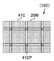
- the adhesive 41LC disposed on the glass wafer 20WC is patterned in substantially the same shape as the imaging chip placement region 30S.
- the adhesive 41LC is patterned by photolithography after applying a photosensitive resin. Application may be performed by spin-coating a liquid adhesive or laminating a film adhesive. Then, the imaging chip 30 is bonded to the glass wafer 20WC by thermocompression bonding through the patterned adhesive 41LC, and the bonded wafer 40WC bonded by the adhesive layer 41C is manufactured.
- the manufacturing method of Modification 3 can be manufactured in a shorter time than a manufacturing method in which an adhesive is arranged before mounting an imaging chip at a number of positions corresponding to each imaging chip 30. Further, since there is no adhesive 41LC between the imaging chips 30, heat is not easily transmitted in the horizontal direction, and the uncured adhesive 41LC of the adjacent imaging chip is cured when the imaging chip 30 is thermally cured. There is no.
- a dam for preventing the sealing resin from flowing out may be formed on the outer periphery of the wafer by patterning the adhesive 41LC.
- An alignment mark for alignment with the imaging chip may be formed by patterning the adhesive 41LC.
- the adhesive 41LD disposed on the glass wafer 20WD is patterned into a frame shape. That is, the adhesive 41LD has a frame shape with a width of 25 ⁇ m or more and 500 ⁇ m or less along the outer periphery of the light receiving unit. For this reason, in the imaging device 10 ⁇ / b> D, the light receiving portion 31 in which a microlens (not shown) is disposed is in contact with the cavity (hollow portion) 38.
- the imaging device 10D has higher sensitivity than the imaging device 10C.
- Such a cavity structure can also be realized by forming a recess at a position corresponding to the light receiving portion of the imaging chip 30 of the glass wafer 20W.
- the imaging device 10D having the cavity 38 and the imaging device 10C having no cavity 38 can be mixed and produced on a single bonded wafer 40WD.
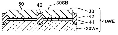
- the frame-shaped groove 26 is formed on the outer peripheral portion of the imaging chip arrangement region 30S of the glass wafer 20WE by, for example, a dicing blade before the bonding process. Is done.
- the groove 26 may be formed by etching, and at the same time, the alignment mark 21 or the like may be formed.
- the imaging chip 30 is heated and pressurized in an aligned state and bonded to the glass wafer 20WE.
- the excessive adhesive 41L flows into the groove 26.
- the fillet does not spread in the horizontal direction (parallel direction of the main surface) nor in the vertical direction (vertical direction of the main surface). Since the fillet does not spread in the horizontal direction, the bonding wafer 40WE can be manufactured from one sheet to a large number of imaging devices 10E by reducing the arrangement interval L of the imaging chips 30.
- the imaging device 10E ensures that the sealing member 42 reaches the outer periphery of the imaging chip 30 in the sealing member filling step. Filled. Since the sealing member 42 can use a resin having a sealing effect higher than that of the adhesive layer 41, the imaging device 10E is more than the imaging device 10 in which the adhesive layer 41 may be exposed to the outer surface due to the rise of the fillet. High reliability.
- a plan view dimension inside the frame-shaped groove 26 smaller than a plan view dimension of the imaging chip 30. This is because when the sealing member 42 is filled, the sealing member 42 covers the outer peripheral portion of the first main surface 30SA of the imaging chip 30, so that the adhesion and sealing performance are improved by the anchor effect.
- the bottom of the groove 26 is curved using the shape of the dicing blade. This is because when the bottom of the groove 26 is rectangular, a void is generated between the flowing adhesive 41L and the corner of the groove 26, and the reliability may be lowered.
- the thermal expansion coefficient of the sealing member 42 on the upper side in the groove 26 is smaller than the thermal expansion coefficient of the adhesive layer 41 on the lower side.
- the thermal expansion coefficient of the imaging chip 30 made of silicon constituting the upper wall surface of the groove 26 is smaller than that of the cover glass 20 made of glass constituting the lower wall surface of the groove 26.
- the cutting trace can be made into the linear form on the wall surface of the groove
- FIG. The cutting trace has an effect of diffusing light and reducing reflection. For this reason, even if the side surface of the cover glass 20 and the light receiving unit 31 are close to each other, flare hardly occurs.
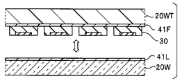
- the second main surface 30SB of the plurality of imaging chips 30 is a second support substrate via the temporary fixing adhesive 41LF. Bonded to a temporary support substrate 20WT.
- the temporary support substrate 20WT may be the same glass as the glass wafer 20W, but need not be transparent.
- the adhesive 41LF is used for temporary fixing in which the adhesive strength is weakened by heat, ultraviolet rays, hot water, or a solvent.
- An alignment mark for alignment with the imaging chip 30 and an alignment mark for alignment with the glass wafer 20W are formed on the temporary support substrate 20WT. Note that an alignment mark may be formed on the back surface of the temporary support substrate 20WT, and alignment with the imaging chip 30 may be performed using the mark.
- the adhesive layer 41F is preferably highly transparent.
- the ring illumination is used as the illumination, the image is easily recognized.
- the first main surfaces 30SA of the plurality of imaging chips 30 adhered to the temporary support substrate 20WT are collectively adhered to the glass wafer 20W via an adhesive 41L. That is, the temporary support substrate 20WT and the glass wafer 20W are aligned and bonded using a wafer aligner and a wafer bonder.
- the imaging chips 30 are thermally cured and bonded one by one to the adhesive 41L applied to the entire surface of the glass wafer 20W, the adhesive 41L in the adjacent imaging chip arrangement region 30S is cured, and the adjacent chips are bonded. There are times when you can't. However, such a problem does not occur in the method for manufacturing the imaging device 10F according to Modification 6.
- the inclination of the main surface of the imaging chip 30 after bonding with respect to the main surface of the glass wafer 20W can be made uniform.
- the space between the imaging chips 30 is sealed with a sealing member 42. That is, the sealing resin 42L is filled in the gap between the temporary support substrate 20WT and the glass wafer 20W.
- the sealing resin 42L may be filled after separating the temporary support substrate 20WT. However, by performing the temporary support substrate 20WT before the separation, the sealing member 42 does not protrude from the second main surface 30SB of the imaging chip 30, and the second main surface 30SB of the imaging chip 30 and the sealing member Since the surfaces of 42 are all flat, the subsequent polishing process is easy.
- the adhesive 41L may be applied to the glass wafer 20W thickly, and when the imaging chip 30 is adhered, the thickly applied adhesive 41L may be filled between the imaging chips 30. That is, in this case, the adhesive 41L also functions as the sealing resin 42L.
- the temporary support substrate 20WT is separated to produce a bonded wafer 40W.
- the subsequent steps are the same as those in FIG. 12D.
- the manufacturing method of the imaging device according to the embodiment and the modified example can manufacture an ultra-compact and highly reliable imaging device, so that the imaging device is particularly disposed at the distal end portion of the electronic endoscope or the capsule endoscope. It can use for the manufacturing method of.
Landscapes
- Engineering & Computer Science (AREA)
- Power Engineering (AREA)
- Physics & Mathematics (AREA)
- Microelectronics & Electronic Packaging (AREA)
- General Physics & Mathematics (AREA)
- Computer Hardware Design (AREA)
- Condensed Matter Physics & Semiconductors (AREA)
- Electromagnetism (AREA)
- Sustainable Development (AREA)
- Life Sciences & Earth Sciences (AREA)
- Signal Processing (AREA)
- Multimedia (AREA)
- Solid State Image Pick-Up Elements (AREA)
- Dicing (AREA)
- Transforming Light Signals Into Electric Signals (AREA)
- Encapsulation Of And Coatings For Semiconductor Or Solid State Devices (AREA)
Priority Applications (5)
| Application Number | Priority Date | Filing Date | Title |
|---|---|---|---|
| CN201380028577.7A CN104380465B (zh) | 2012-05-30 | 2013-04-04 | 摄像装置的制造方法以及半导体装置的制造方法 |
| JP2014518322A JP6395600B2 (ja) | 2012-05-30 | 2013-04-04 | 撮像装置の製造方法および半導体装置の製造方法 |
| EP13796612.3A EP2858111B1 (de) | 2012-05-30 | 2013-04-04 | Herstellungsverfahren für bildgebungsvorrichtung und herstellungsverfahren für halbleiterbauelement |
| US14/557,271 US9282261B2 (en) | 2012-05-30 | 2014-12-01 | Method for producing image pickup apparatus and method for producing semiconductor apparatus |
| US14/994,581 US9698195B2 (en) | 2012-05-30 | 2016-01-13 | Method for producing image pickup apparatus and method for producing semiconductor apparatus |
Applications Claiming Priority (2)
| Application Number | Priority Date | Filing Date | Title |
|---|---|---|---|
| JP2012-123223 | 2012-05-30 | ||
| JP2012123223 | 2012-05-30 |
Related Child Applications (1)
| Application Number | Title | Priority Date | Filing Date |
|---|---|---|---|
| US14/557,271 Continuation US9282261B2 (en) | 2012-05-30 | 2014-12-01 | Method for producing image pickup apparatus and method for producing semiconductor apparatus |
Publications (1)
| Publication Number | Publication Date |
|---|---|
| WO2013179765A1 true WO2013179765A1 (ja) | 2013-12-05 |
Family
ID=49672973
Family Applications (1)
| Application Number | Title | Priority Date | Filing Date |
|---|---|---|---|
| PCT/JP2013/060343 WO2013179765A1 (ja) | 2012-05-30 | 2013-04-04 | 撮像装置の製造方法および半導体装置の製造方法 |
Country Status (5)
| Country | Link |
|---|---|
| US (2) | US9282261B2 (de) |
| EP (1) | EP2858111B1 (de) |
| JP (1) | JP6395600B2 (de) |
| CN (1) | CN104380465B (de) |
| WO (1) | WO2013179765A1 (de) |
Cited By (7)
| Publication number | Priority date | Publication date | Assignee | Title |
|---|---|---|---|---|
| WO2015099140A1 (ja) * | 2013-12-27 | 2015-07-02 | 株式会社ニコン | 撮像ユニット及び撮像装置 |
| CN106031150A (zh) * | 2014-02-24 | 2016-10-12 | 奥林巴斯株式会社 | 摄像装置和摄像装置的制造方法 |
| JP2017526977A (ja) * | 2014-05-16 | 2017-09-14 | ヘプタゴン・マイクロ・オプティクス・プライベート・リミテッドHeptagon Micro Optics Pte. Ltd. | 装置の、特に光学装置のウェーハレベル製造 |
| WO2020021666A1 (ja) * | 2018-07-25 | 2020-01-30 | 株式会社Fuji | 決定装置及びこれを備えるチップ装着装置 |
| CN110993490A (zh) * | 2019-12-30 | 2020-04-10 | 长春长光圆辰微电子技术有限公司 | 一种不同尺寸芯片实现异质键合的方法 |
| JP2021048215A (ja) * | 2019-09-18 | 2021-03-25 | 大日本印刷株式会社 | 半導体多面付け基板用部材、半導体多面付け基板、および半導体部材 |
| WO2021193266A1 (ja) * | 2020-03-27 | 2021-09-30 | ソニーセミコンダクタソリューションズ株式会社 | 固体撮像装置 |
Families Citing this family (21)
| Publication number | Priority date | Publication date | Assignee | Title |
|---|---|---|---|---|
| US9067621B2 (en) * | 2010-12-06 | 2015-06-30 | Honda Motor Co., Ltd. | Subframe structure |
| EP2858112A4 (de) * | 2012-05-30 | 2016-04-13 | Olympus Corp | Verfahren zur herstellung einer bildgebungsvorrichtung und verfahren zur herstellung eines halbleiterbauelements |
| US10446728B2 (en) * | 2014-10-31 | 2019-10-15 | eLux, Inc. | Pick-and remove system and method for emissive display repair |
| US9799625B2 (en) | 2015-06-12 | 2017-10-24 | Taiwan Semiconductor Manufacturing Company Ltd. | Semiconductor structure and manufacturing method thereof |
| WO2016203797A1 (ja) * | 2015-06-16 | 2016-12-22 | オリンパス株式会社 | 撮像モジュール、内視鏡システムおよび撮像モジュールの製造方法 |
| JP2017199834A (ja) * | 2016-04-28 | 2017-11-02 | 株式会社ジェイデバイス | 半導体パッケージ及び半導体パッケージの製造方法 |
| CN107777657A (zh) * | 2016-08-25 | 2018-03-09 | 中芯国际集成电路制造(上海)有限公司 | 一种mems器件及其制备方法和电子装置 |
| WO2018125162A1 (en) * | 2016-12-29 | 2018-07-05 | Intel Corporation | Semiconductor package having passive support wafer |
| TWI771375B (zh) | 2017-02-24 | 2022-07-21 | 美商康寧公司 | 高寬高比玻璃晶圓 |
| JP2019160866A (ja) * | 2018-03-08 | 2019-09-19 | ソニーセミコンダクタソリューションズ株式会社 | 撮像装置 |
| CN111868920A (zh) * | 2018-03-15 | 2020-10-30 | 应用材料公司 | 用于半导体器件封装制造工艺的平坦化 |
| JP2019213151A (ja) * | 2018-06-08 | 2019-12-12 | ソニーセミコンダクタソリューションズ株式会社 | 撮像装置 |
| KR102477355B1 (ko) * | 2018-10-23 | 2022-12-15 | 삼성전자주식회사 | 캐리어 기판 및 이를 이용한 기판 처리 장치 |
| WO2020089960A1 (ja) * | 2018-10-29 | 2020-05-07 | オリンパス株式会社 | 撮像装置、内視鏡、および、撮像装置の製造方法 |
| CN113329676B (zh) | 2019-03-18 | 2024-05-24 | 奥林巴斯株式会社 | 保持框、内窥镜前端构造以及内窥镜 |
| KR20220006559A (ko) * | 2019-05-08 | 2022-01-17 | 도쿄엘렉트론가부시키가이샤 | 접합 장치, 접합 시스템 및 접합 방법 |
| US20220223483A1 (en) * | 2019-05-22 | 2022-07-14 | Vuereal Inc. | An alignment process for the transfer setup |
| US11742437B2 (en) | 2020-03-27 | 2023-08-29 | Stmicroelectronics Ltd | WLCSP with transparent substrate and method of manufacturing the same |
| TWI748599B (zh) * | 2020-08-14 | 2021-12-01 | 矽品精密工業股份有限公司 | 晶片整配系統及晶片整配方法 |
| KR20220065292A (ko) | 2020-11-13 | 2022-05-20 | 삼성전자주식회사 | 반도체 패키지 및 그의 제조 방법 |
| CN112992699B (zh) * | 2021-02-01 | 2024-03-22 | 上海易卜半导体有限公司 | 半导体封装方法、半导体组件以及包含其的电子设备 |
Citations (6)
| Publication number | Priority date | Publication date | Assignee | Title |
|---|---|---|---|---|
| JP2006128625A (ja) * | 2004-09-30 | 2006-05-18 | Oki Electric Ind Co Ltd | 半導体装置及びその製造方法 |
| JP2008130738A (ja) * | 2006-11-20 | 2008-06-05 | Fujifilm Corp | 固体撮像素子 |
| JP2008235401A (ja) * | 2007-03-19 | 2008-10-02 | Spansion Llc | 半導体装置及びその製造方法 |
| JP2009537970A (ja) * | 2006-05-19 | 2009-10-29 | オスラム オプト セミコンダクターズ ゲゼルシャフト ミット ベシュレンクテル ハフツング | 絶縁性接続媒体を用いた電気伝導性接続部 |
| JP2010120145A (ja) * | 2008-11-21 | 2010-06-03 | Toshiba Corp | Memsパッケージおよびmemsパッケージの製造方法 |
| JP2011243596A (ja) | 2010-05-14 | 2011-12-01 | Panasonic Corp | パッケージ部品の製造方法およびパッケージ部品 |
Family Cites Families (22)
| Publication number | Priority date | Publication date | Assignee | Title |
|---|---|---|---|---|
| JPH0513570A (ja) * | 1991-07-05 | 1993-01-22 | Nec Corp | 半導体装置の製造方法 |
| JPH09260581A (ja) * | 1996-03-19 | 1997-10-03 | Hitachi Ltd | 複合半導体装置の製造方法 |
| JP4234269B2 (ja) * | 1999-07-16 | 2009-03-04 | 浜松ホトニクス株式会社 | 半導体装置及びその製造方法 |
| JP4530497B2 (ja) * | 2000-07-24 | 2010-08-25 | オリンパス株式会社 | 撮像装置 |
| JP4045083B2 (ja) * | 2000-12-25 | 2008-02-13 | 株式会社ルネサステクノロジ | 半導体モジュールおよび実装構造体 |
| JP2002231920A (ja) * | 2001-02-06 | 2002-08-16 | Olympus Optical Co Ltd | 固体撮像装置及びその製造方法 |
| JP4663184B2 (ja) * | 2001-09-26 | 2011-03-30 | パナソニック株式会社 | 半導体装置の製造方法 |
| JP2003335922A (ja) * | 2002-05-20 | 2003-11-28 | Kyocera Chemical Corp | 封止用樹脂組成物および樹脂封止型半導体装置 |
| US7180149B2 (en) * | 2003-08-28 | 2007-02-20 | Fujikura Ltd. | Semiconductor package with through-hole |
| TWI231606B (en) * | 2003-11-10 | 2005-04-21 | Shih-Hsien Tseng | Image pickup device and a manufacturing method thereof |
| JP3739375B2 (ja) * | 2003-11-28 | 2006-01-25 | 沖電気工業株式会社 | 半導体装置及びその製造方法 |
| JP3945482B2 (ja) * | 2004-01-26 | 2007-07-18 | 松下電工株式会社 | 半導体封止用樹脂組成物とそれを用いた半導体装置 |
| CN101449368A (zh) * | 2006-05-19 | 2009-06-03 | 奥斯兰姆奥普托半导体有限责任公司 | 具有绝缘连接介质的导电连接 |
| JP2007317822A (ja) * | 2006-05-25 | 2007-12-06 | Sony Corp | 基板処理方法及び半導体装置の製造方法 |
| JP5423399B2 (ja) * | 2008-01-09 | 2014-02-19 | 日本電気株式会社 | コンデンサ内蔵装置の製造方法及びコンデンサ内蔵パッケージの製造方法 |
| JP4799594B2 (ja) * | 2008-08-19 | 2011-10-26 | 株式会社東芝 | 固体撮像装置およびその製造方法 |
| JP5317586B2 (ja) * | 2008-08-28 | 2013-10-16 | ラピスセミコンダクタ株式会社 | カメラモジュール及びその製造方法 |
| JP2010212297A (ja) * | 2009-03-06 | 2010-09-24 | Toshiba Corp | 半導体装置および半導体装置の製造方法 |
| JP2010263199A (ja) * | 2009-04-07 | 2010-11-18 | Furukawa Electric Co Ltd:The | 半導体装置の製造方法および半導体装置 |
| TWI513301B (zh) * | 2010-06-02 | 2015-12-11 | Sony Corp | 半導體裝置,固態成像裝置及相機系統 |
| JP5682185B2 (ja) * | 2010-09-07 | 2015-03-11 | ソニー株式会社 | 半導体パッケージおよび半導体パッケージの製造方法ならびに光学モジュール |
| JP5811456B2 (ja) * | 2010-12-28 | 2015-11-11 | 株式会社Gsユアサ | 蓄電素子 |
-
2013
- 2013-04-04 WO PCT/JP2013/060343 patent/WO2013179765A1/ja active Application Filing
- 2013-04-04 EP EP13796612.3A patent/EP2858111B1/de active Active
- 2013-04-04 JP JP2014518322A patent/JP6395600B2/ja active Active
- 2013-04-04 CN CN201380028577.7A patent/CN104380465B/zh not_active Expired - Fee Related
-
2014
- 2014-12-01 US US14/557,271 patent/US9282261B2/en active Active
-
2016
- 2016-01-13 US US14/994,581 patent/US9698195B2/en active Active
Patent Citations (6)
| Publication number | Priority date | Publication date | Assignee | Title |
|---|---|---|---|---|
| JP2006128625A (ja) * | 2004-09-30 | 2006-05-18 | Oki Electric Ind Co Ltd | 半導体装置及びその製造方法 |
| JP2009537970A (ja) * | 2006-05-19 | 2009-10-29 | オスラム オプト セミコンダクターズ ゲゼルシャフト ミット ベシュレンクテル ハフツング | 絶縁性接続媒体を用いた電気伝導性接続部 |
| JP2008130738A (ja) * | 2006-11-20 | 2008-06-05 | Fujifilm Corp | 固体撮像素子 |
| JP2008235401A (ja) * | 2007-03-19 | 2008-10-02 | Spansion Llc | 半導体装置及びその製造方法 |
| JP2010120145A (ja) * | 2008-11-21 | 2010-06-03 | Toshiba Corp | Memsパッケージおよびmemsパッケージの製造方法 |
| JP2011243596A (ja) | 2010-05-14 | 2011-12-01 | Panasonic Corp | パッケージ部品の製造方法およびパッケージ部品 |
Non-Patent Citations (1)
| Title |
|---|
| See also references of EP2858111A4 |
Cited By (12)
| Publication number | Priority date | Publication date | Assignee | Title |
|---|---|---|---|---|
| WO2015099140A1 (ja) * | 2013-12-27 | 2015-07-02 | 株式会社ニコン | 撮像ユニット及び撮像装置 |
| CN106031150A (zh) * | 2014-02-24 | 2016-10-12 | 奥林巴斯株式会社 | 摄像装置和摄像装置的制造方法 |
| US10381393B2 (en) | 2014-02-24 | 2019-08-13 | Olympus Corporation | Image pickup apparatus and method for manufacturing image pickup apparatus |
| JP2017526977A (ja) * | 2014-05-16 | 2017-09-14 | ヘプタゴン・マイクロ・オプティクス・プライベート・リミテッドHeptagon Micro Optics Pte. Ltd. | 装置の、特に光学装置のウェーハレベル製造 |
| US10682824B2 (en) | 2014-05-16 | 2020-06-16 | Ams Sensors Singapore Pte. Ltd. | Wafer-level manufacture of devices, in particular of optical devices |
| WO2020021666A1 (ja) * | 2018-07-25 | 2020-01-30 | 株式会社Fuji | 決定装置及びこれを備えるチップ装着装置 |
| JPWO2020021666A1 (ja) * | 2018-07-25 | 2021-02-15 | 株式会社Fuji | 決定装置及びこれを備えるチップ装着装置 |
| JP7068460B2 (ja) | 2018-07-25 | 2022-05-16 | 株式会社Fuji | 決定装置及びこれを備えるチップ装着装置 |
| JP2021048215A (ja) * | 2019-09-18 | 2021-03-25 | 大日本印刷株式会社 | 半導体多面付け基板用部材、半導体多面付け基板、および半導体部材 |
| JP7395898B2 (ja) | 2019-09-18 | 2023-12-12 | 大日本印刷株式会社 | 半導体多面付け基板用部材、半導体多面付け基板、および半導体部材 |
| CN110993490A (zh) * | 2019-12-30 | 2020-04-10 | 长春长光圆辰微电子技术有限公司 | 一种不同尺寸芯片实现异质键合的方法 |
| WO2021193266A1 (ja) * | 2020-03-27 | 2021-09-30 | ソニーセミコンダクタソリューションズ株式会社 | 固体撮像装置 |
Also Published As
| Publication number | Publication date |
|---|---|
| US20160126286A1 (en) | 2016-05-05 |
| EP2858111B1 (de) | 2019-06-26 |
| US9282261B2 (en) | 2016-03-08 |
| CN104380465A (zh) | 2015-02-25 |
| CN104380465B (zh) | 2018-02-09 |
| JPWO2013179765A1 (ja) | 2016-01-18 |
| US20150085169A1 (en) | 2015-03-26 |
| EP2858111A1 (de) | 2015-04-08 |
| US9698195B2 (en) | 2017-07-04 |
| JP6395600B2 (ja) | 2018-09-26 |
| EP2858111A4 (de) | 2016-04-13 |
Similar Documents
| Publication | Publication Date | Title |
|---|---|---|
| JP6395600B2 (ja) | 撮像装置の製造方法および半導体装置の製造方法 | |
| JP6315859B2 (ja) | 撮像装置、半導体装置および撮像ユニット | |
| US9240398B2 (en) | Method for producing image pickup apparatus and method for producing semiconductor apparatus | |
| JP6147250B2 (ja) | 撮像装置の製造方法および半導体装置の製造方法 | |
| US7061106B2 (en) | Structure of image sensor module and a method for manufacturing of wafer level package | |
| US7192805B2 (en) | Semiconductor device and method of manufacturing the same | |
| JP4542768B2 (ja) | 固体撮像装置及びその製造方法 | |
| TWI539538B (zh) | 半導體裝置及其製造方法 | |
| JP2006049700A (ja) | 固体撮像装置の製造方法 | |
| US20230395633A1 (en) | Image sensor packaging structures and related methods |
Legal Events
| Date | Code | Title | Description |
|---|---|---|---|
| 121 | Ep: the epo has been informed by wipo that ep was designated in this application |
Ref document number: 13796612 Country of ref document: EP Kind code of ref document: A1 |
|
| ENP | Entry into the national phase |
Ref document number: 2014518322 Country of ref document: JP Kind code of ref document: A |
|
| NENP | Non-entry into the national phase |
Ref country code: DE |
|
| WWE | Wipo information: entry into national phase |
Ref document number: 2013796612 Country of ref document: EP |