WO2013141318A1 - 透明導電性積層体及び電子デバイス又はモジュール - Google Patents
透明導電性積層体及び電子デバイス又はモジュール Download PDFInfo
- Publication number
- WO2013141318A1 WO2013141318A1 PCT/JP2013/058139 JP2013058139W WO2013141318A1 WO 2013141318 A1 WO2013141318 A1 WO 2013141318A1 JP 2013058139 W JP2013058139 W JP 2013058139W WO 2013141318 A1 WO2013141318 A1 WO 2013141318A1
- Authority
- WO
- WIPO (PCT)
- Prior art keywords
- group
- transparent conductive
- layer
- conductive laminate
- refractive layer
- Prior art date
Links
- 0 CN([*+])[Si+]N(C)[*+]N1[*+]N([Si+]N[Si+]N2[Si+]N[*+]N(C)[*+]N[*+]2)[Si+]N[*+]1 Chemical compound CN([*+])[Si+]N(C)[*+]N1[*+]N([Si+]N[Si+]N2[Si+]N[*+]N(C)[*+]N[*+]2)[Si+]N[*+]1 0.000 description 1
Classifications
-
- H—ELECTRICITY
- H05—ELECTRIC TECHNIQUES NOT OTHERWISE PROVIDED FOR
- H05K—PRINTED CIRCUITS; CASINGS OR CONSTRUCTIONAL DETAILS OF ELECTRIC APPARATUS; MANUFACTURE OF ASSEMBLAGES OF ELECTRICAL COMPONENTS
- H05K1/00—Printed circuits
- H05K1/02—Details
- H05K1/0274—Optical details, e.g. printed circuits comprising integral optical means
-
- C—CHEMISTRY; METALLURGY
- C04—CEMENTS; CONCRETE; ARTIFICIAL STONE; CERAMICS; REFRACTORIES
- C04B—LIME, MAGNESIA; SLAG; CEMENTS; COMPOSITIONS THEREOF, e.g. MORTARS, CONCRETE OR LIKE BUILDING MATERIALS; ARTIFICIAL STONE; CERAMICS; REFRACTORIES; TREATMENT OF NATURAL STONE
- C04B35/00—Shaped ceramic products characterised by their composition; Ceramics compositions; Processing powders of inorganic compounds preparatory to the manufacturing of ceramic products
- C04B35/01—Shaped ceramic products characterised by their composition; Ceramics compositions; Processing powders of inorganic compounds preparatory to the manufacturing of ceramic products based on oxide ceramics
- C04B35/453—Shaped ceramic products characterised by their composition; Ceramics compositions; Processing powders of inorganic compounds preparatory to the manufacturing of ceramic products based on oxide ceramics based on zinc, tin, or bismuth oxides or solid solutions thereof with other oxides, e.g. zincates, stannates or bismuthates
-
- G—PHYSICS
- G02—OPTICS
- G02F—OPTICAL DEVICES OR ARRANGEMENTS FOR THE CONTROL OF LIGHT BY MODIFICATION OF THE OPTICAL PROPERTIES OF THE MEDIA OF THE ELEMENTS INVOLVED THEREIN; NON-LINEAR OPTICS; FREQUENCY-CHANGING OF LIGHT; OPTICAL LOGIC ELEMENTS; OPTICAL ANALOGUE/DIGITAL CONVERTERS
- G02F1/00—Devices or arrangements for the control of the intensity, colour, phase, polarisation or direction of light arriving from an independent light source, e.g. switching, gating or modulating; Non-linear optics
- G02F1/01—Devices or arrangements for the control of the intensity, colour, phase, polarisation or direction of light arriving from an independent light source, e.g. switching, gating or modulating; Non-linear optics for the control of the intensity, phase, polarisation or colour
- G02F1/13—Devices or arrangements for the control of the intensity, colour, phase, polarisation or direction of light arriving from an independent light source, e.g. switching, gating or modulating; Non-linear optics for the control of the intensity, phase, polarisation or colour based on liquid crystals, e.g. single liquid crystal display cells
- G02F1/133—Constructional arrangements; Operation of liquid crystal cells; Circuit arrangements
- G02F1/1333—Constructional arrangements; Manufacturing methods
- G02F1/1343—Electrodes
- G02F1/13439—Electrodes characterised by their electrical, optical, physical properties; materials therefor; method of making
-
- G—PHYSICS
- G06—COMPUTING; CALCULATING OR COUNTING
- G06F—ELECTRIC DIGITAL DATA PROCESSING
- G06F3/00—Input arrangements for transferring data to be processed into a form capable of being handled by the computer; Output arrangements for transferring data from processing unit to output unit, e.g. interface arrangements
- G06F3/01—Input arrangements or combined input and output arrangements for interaction between user and computer
- G06F3/03—Arrangements for converting the position or the displacement of a member into a coded form
- G06F3/041—Digitisers, e.g. for touch screens or touch pads, characterised by the transducing means
-
- H—ELECTRICITY
- H05—ELECTRIC TECHNIQUES NOT OTHERWISE PROVIDED FOR
- H05K—PRINTED CIRCUITS; CASINGS OR CONSTRUCTIONAL DETAILS OF ELECTRIC APPARATUS; MANUFACTURE OF ASSEMBLAGES OF ELECTRICAL COMPONENTS
- H05K1/00—Printed circuits
- H05K1/02—Details
- H05K1/03—Use of materials for the substrate
- H05K1/0313—Organic insulating material
- H05K1/0353—Organic insulating material consisting of two or more materials, e.g. two or more polymers, polymer + filler, + reinforcement
-
- C—CHEMISTRY; METALLURGY
- C04—CEMENTS; CONCRETE; ARTIFICIAL STONE; CERAMICS; REFRACTORIES
- C04B—LIME, MAGNESIA; SLAG; CEMENTS; COMPOSITIONS THEREOF, e.g. MORTARS, CONCRETE OR LIKE BUILDING MATERIALS; ARTIFICIAL STONE; CERAMICS; REFRACTORIES; TREATMENT OF NATURAL STONE
- C04B2235/00—Aspects relating to ceramic starting mixtures or sintered ceramic products
- C04B2235/02—Composition of constituents of the starting material or of secondary phases of the final product
- C04B2235/30—Constituents and secondary phases not being of a fibrous nature
- C04B2235/32—Metal oxides, mixed metal oxides, or oxide-forming salts thereof, e.g. carbonates, nitrates, (oxy)hydroxides, chlorides
- C04B2235/3284—Zinc oxides, zincates, cadmium oxides, cadmiates, mercury oxides, mercurates or oxide forming salts thereof
-
- C—CHEMISTRY; METALLURGY
- C04—CEMENTS; CONCRETE; ARTIFICIAL STONE; CERAMICS; REFRACTORIES
- C04B—LIME, MAGNESIA; SLAG; CEMENTS; COMPOSITIONS THEREOF, e.g. MORTARS, CONCRETE OR LIKE BUILDING MATERIALS; ARTIFICIAL STONE; CERAMICS; REFRACTORIES; TREATMENT OF NATURAL STONE
- C04B2235/00—Aspects relating to ceramic starting mixtures or sintered ceramic products
- C04B2235/02—Composition of constituents of the starting material or of secondary phases of the final product
- C04B2235/30—Constituents and secondary phases not being of a fibrous nature
- C04B2235/32—Metal oxides, mixed metal oxides, or oxide-forming salts thereof, e.g. carbonates, nitrates, (oxy)hydroxides, chlorides
- C04B2235/3286—Gallium oxides, gallates, indium oxides, indates, thallium oxides, thallates or oxide forming salts thereof, e.g. zinc gallate
-
- H—ELECTRICITY
- H05—ELECTRIC TECHNIQUES NOT OTHERWISE PROVIDED FOR
- H05K—PRINTED CIRCUITS; CASINGS OR CONSTRUCTIONAL DETAILS OF ELECTRIC APPARATUS; MANUFACTURE OF ASSEMBLAGES OF ELECTRICAL COMPONENTS
- H05K2201/00—Indexing scheme relating to printed circuits covered by H05K1/00
- H05K2201/03—Conductive materials
- H05K2201/032—Materials
- H05K2201/0326—Inorganic, non-metallic conductor, e.g. indium-tin oxide [ITO]
-
- Y—GENERAL TAGGING OF NEW TECHNOLOGICAL DEVELOPMENTS; GENERAL TAGGING OF CROSS-SECTIONAL TECHNOLOGIES SPANNING OVER SEVERAL SECTIONS OF THE IPC; TECHNICAL SUBJECTS COVERED BY FORMER USPC CROSS-REFERENCE ART COLLECTIONS [XRACs] AND DIGESTS
- Y10—TECHNICAL SUBJECTS COVERED BY FORMER USPC
- Y10T—TECHNICAL SUBJECTS COVERED BY FORMER US CLASSIFICATION
- Y10T428/00—Stock material or miscellaneous articles
- Y10T428/24—Structurally defined web or sheet [e.g., overall dimension, etc.]
- Y10T428/24942—Structurally defined web or sheet [e.g., overall dimension, etc.] including components having same physical characteristic in differing degree
Definitions
- the present invention relates to a transparent conductive laminate excellent in moisture and heat resistance and optical characteristics, and an electronic device or module using the transparent conductive laminate.
- the plastic film has a problem that it easily permeates water vapor, oxygen, and the like as compared with the glass plate, and easily causes deterioration of elements inside the electronic member.
- Patent Document 1 includes a transparent base material and a transparent conductive film, and has an extinction coefficient of 0.05 or less with respect to a light beam having a wavelength of 550 nm and a yellowness (YI) of 0.1.
- the films obtained in the examples of this document are not satisfactory in both heat and heat resistance and optical properties, and further improvement in performance has been desired.
- the present invention has been made in view of such circumstances, and provides a transparent conductive laminate excellent in moisture and heat resistance and optical characteristics, and an electronic device or module using the transparent conductive laminate. Objective.
- a low refractive index layer and an intermediate refractive layer are formed on at least one surface of the base material directly or through one or more layers in order from the base material side.
- a transparent conductive laminate formed by laminating a transparent conductive layer, wherein the refractive index of the low refractive layer and the refractive index and film density of the intermediate refractive layer are in a specific range, are excellent in moisture and heat resistance.
- the present inventors have found that the yellow color is suppressed and the optical properties are excellent, and the present invention has been completed.
- the following transparent conductive laminates (1) to (6) are provided.
- a transparent conductive laminate formed by laminating a low refractive layer, an intermediate refractive layer, and a transparent conductive layer on at least one surface of a base material directly or via one or more layers in order from the base material side.
- the refractive index of the low refractive layer is 1.40 to 1.50
- the refractive index of the intermediate refractive layer is 1.50 to 1.80
- the film density of the intermediate refractive layer is 2.5 to 4.
- a transparent conductive laminate which is 5 g / cm 3 .
- the transparent conductive laminate according to (1) wherein the low refractive layer has an optical film thickness of 10 to 800 nm.
- the transparent conductive laminate according to (1) which has a water vapor transmission rate of 0.1 g / m 2 / day or less in an atmosphere of 40 ° C. and 90% relative humidity.
- the transparent conductive laminate according to (1) which has a transmission hue b * value of ⁇ 2.0 to +2.0 and a total light transmittance of 80% or more.
- the material constituting the transparent conductive layer is at least one selected from the group consisting of zinc oxide, zinc oxide doped with gallium (GZO), zinc oxide doped with aluminum (AZO), and indium zinc oxide (IZO).
- the transparent conductive laminate according to (1) which is a seed.
- the transparent conductive laminate according to (1), wherein the intermediate refractive layer and the low refractive layer are layers obtained by subjecting a silicon-based polymer layer to ion implantation.
- the transparent conductive laminate of the present invention is excellent in moisture and heat resistance, has a yellowish color, and has excellent optical characteristics. Therefore, an electronic device used in an image display device such as a liquid crystal display, an electroluminescence (EL) display, or a touch panel. It is suitable as a member. Since the electronic device or module of the present invention uses the transparent conductive laminate of the present invention, it is excellent in moisture and heat resistance, suppressed yellowishness, and excellent in optical characteristics.
- the transparent conductive laminate of the present invention is formed by laminating a low refractive layer, an intermediate refractive layer, and a transparent conductive layer on at least one surface of a substrate directly or via one or more layers in order from the substrate side.
- a transparent conductive laminate having a refractive index of a low refractive layer of 1.40 to 1.50, a refractive index of an intermediate refractive layer of 1.50 to 1.80, and a film density of the intermediate refractive layer Is 2.5 to 4.5.
- the substrate used in the present invention is not particularly limited as long as it is colorless and transparent and has sufficient strength as a substrate of the transparent conductive laminate.
- Materials for the base material include polyimide, polyamide, polyamideimide, polyphenylene ether, polyether ketone, polyether ether ketone, polyolefin, polyester, polycarbonate, polysulfone, polyethersulfone, polyphenylene sulfide, polyarylate, acrylic resin, cyclohexane Examples include olefin polymers, aromatic polymers, polyurethane polymers, and the like.
- polyester since it is excellent in transparency and has versatility, polyester, polyamide or cycloolefin polymer is preferable, and polyester or cycloolefin polymer is more preferable.
- polyester include polyethylene terephthalate, polybutylene terephthalate, polyethylene naphthalate, and polyarylate.
- polyamide include wholly aromatic polyamide, nylon 6, nylon 66, nylon copolymer, and the like.
- cycloolefin polymers include norbornene polymers, monocyclic olefin polymers, cyclic conjugated diene polymers, vinyl alicyclic hydrocarbon polymers, and hydrides thereof.
- polyesters such as polyethylene terephthalate, polybutylene terephthalate, polyethylene naphthalate, and polyarylate are preferable, and polyethylene terephthalate is more preferable.
- the base material may contain various additives such as an antioxidant, a flame retardant, and a lubricant as long as transparency and the like are not impaired.
- the thickness of the substrate is usually 0.01 to 0.5 mm, preferably 0.05 to 0.25 mm. When the thickness of the substrate is within this range, a transparent conductive laminate excellent in transparency and flexibility can be easily obtained.
- the total light transmittance of the substrate is preferably 70% or more, more preferably 70 to 100%, and still more preferably 80 to 95%.
- the haze value of the substrate is preferably 10% or less, more preferably 1 to 10%. When the total light transmittance and haze value of the substrate are within these ranges, a transparent conductive laminate having excellent transparency can be easily obtained.
- the refractive index of the substrate varies depending on the material and the presence or absence of stretching, but is usually in the range of 1.45 to 1.75, preferably 1.6 to 1.75 from the viewpoint of transparency.
- the low refractive layer used in the transparent conductive laminate of the present invention is a layer having a refractive index of 1.40 to 1.50, preferably 1.42 to 1.48.
- a transparent conductive laminate excellent in optical properties can be obtained by using a low refractive layer having such properties in combination with an intermediate refractive layer described later.
- the low refractive layer has an optical film thickness of usually 10 to 800 nm, preferably 100 to 500 nm. When the optical film thickness of the low refractive layer is within this range, a thin transparent conductive laminate having excellent optical characteristics can be obtained.
- the optical film thickness refers to the product (n ⁇ d) of the refractive index (n) of the layer and the film thickness (d) of the layer.
- the low refractive layer has the above-mentioned characteristics, its constituent components and formation method are not particularly limited, and known ones can be used.
- a material for the low refractive layer a silicon polymer compound; a photopolymerizable composition comprising a photopolymerizable monomer and / or a photopolymerizable prepolymer, and a photopolymerization initiator; a polyester resin; Polyurethane resins (particularly polyacrylic polyols, polyester polyols, polyether polyols, etc.
- sicon-based polymer layers are preferable.
- a part of the silicon polymer layer can be modified, and an intermediate refractive layer having desired characteristics can be easily formed. Can be formed.
- the modified portion (hereinafter sometimes referred to as the surface layer portion) becomes an intermediate refractive layer having the desired characteristics, and the unmodified portion becomes a low refractive layer, so that the silicon-based polymer layer is used as the low refractive layer.
- the silicon-based polymer compound may be an organic compound or an inorganic compound as long as it is a silicon-containing polymer.
- examples include polyorganosiloxane compounds, polycarbosilane compounds, polysilane compounds, polysilazane compounds, and the like.
- the polyorganosiloxane compound is a compound obtained by polycondensation of a silane compound having a hydrolyzable functional group.
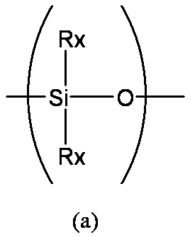
- linear main chain structure is a structure represented by the following formula (a)
- ladder main chain structure is a structure represented by the following formula (b): a cage main chain structure
- each of Rx, Ry, and Rz independently represents a hydrogen atom, an unsubstituted or substituted alkyl group, an unsubstituted or substituted alkenyl group, an unsubstituted or substituted aryl group, etc. Represents a hydrolyzable group.
- the plurality of Rx in the formula (a), the plurality of Ry in the formula (b), and the plurality of Rz in the formula (c) may be the same or different. However, both Rx in the formula (a) are not hydrogen atoms.
- alkyl group of the unsubstituted or substituted alkyl group examples include, for example, methyl group, ethyl group, n-propyl group, isopropyl group, n-butyl group, isobutyl group, sec-butyl group, t-butyl group, n
- alkyl groups having 1 to 10 carbon atoms such as -pentyl group, isopentyl group, neopentyl group, n-hexyl group, n-heptyl group and n-octyl group.
- alkenyl group of an unsubstituted or substituted alkenyl group examples include, for example, a vinyl group, 1-propenyl group, 2-propenyl group, 1-butenyl group, 2-butenyl group, 3-butenyl group and the like having 2 to 2 carbon atoms. 10 alkenyl groups are mentioned.
- substituent for the alkyl group and alkenyl group examples include halogen atoms such as fluorine atom, chlorine atom, bromine atom and iodine atom; hydroxyl group; thiol group; epoxy group; glycidoxy group; (meth) acryloyloxy group; And unsubstituted or substituted aryl groups such as 4-methylphenyl group and 4-chlorophenyl group.
- aryl group of an unsubstituted or substituted aryl group examples include aryl groups having 6 to 10 carbon atoms such as a phenyl group, a 1-naphthyl group, and a 2-naphthyl group.
- substituent of the aryl group examples include halogen atoms such as fluorine atom, chlorine atom, bromine atom and iodine atom; alkyl groups having 1 to 6 carbon atoms such as methyl group and ethyl group; carbon numbers such as methoxy group and ethoxy group 1-6 alkoxy groups; nitro groups; cyano groups; hydroxyl groups; thiol groups; epoxy groups; glycidoxy groups; (meth) acryloyloxy groups; unsubstituted phenyl groups, 4-methylphenyl groups, 4-chlorophenyl groups, etc.
- Rx, Ry, and Rz a hydrogen atom, an alkyl group having 1 to 6 carbon atoms, or a phenyl group is preferable, and an alkyl group having 1 to 6 carbon atoms is particularly preferable.
- polysiloxane-based compound As the polyorganosiloxane-based compound, a linear compound represented by the above formula (a) is preferable. From the viewpoint of easy availability and formation of a layer having excellent gas barrier properties, 2 in the above formula (a). Polydimethylsiloxane in which two Rx are both methyl group compounds is more preferable.
- the polyorganosiloxane compound can be obtained, for example, by a known production method in which a silane compound having a hydrolyzable functional group is polycondensed.
- the silane compound to be used may be appropriately selected according to the structure of the target polyorganosiloxane compound.
- Preferred specific examples include bifunctional silane compounds such as dimethyldimethoxysilane, dimethyldiethoxysilane, diethyldimethoxysilane, and diethyldiethoxysilane; methyltrimethoxysilane, methyltriethoxysilane, ethyltrimethoxysilane, ethyltriethoxysilane, trifunctional silane compounds such as n-propyltrimethoxysilane, n-butyltriethoxysilane, phenyltrimethoxysilane, phenyltriethoxysilane, phenyldiethoxymethoxysilane; tetramethoxysilane, tetraethoxysilane, tetra-n-propoxysilane, Tetraisopropoxysilane, tetra-
- the polycarbosilane compound is a polymer compound having a (—Si—C—) bond in the main chain in the molecule.
- a polycarbosilane type compound used for this invention what contains the repeating unit represented by following formula (d) is preferable.
- Rw and Rv each independently represent a hydrogen atom, a hydroxyl group, an alkyl group, an aryl group, an alkenyl group, or a monovalent heterocyclic group.
- a plurality of Rw and Rv may be the same or different.
- alkyl group, aryl group, and alkenyl group of Rw and Rv include the same groups as those exemplified as Rx and the like.
- the heterocyclic ring of the monovalent heterocyclic group is not particularly limited as long as it is a 3- to 10-membered cyclic compound containing at least one hetero atom such as an oxygen atom, a nitrogen atom, or a sulfur atom in addition to a carbon atom.
- Specific examples of the monovalent heterocyclic group include 2-pyridyl group, 3-pyridyl group, 4-pyridyl group, 2-thienyl group, 3-thienyl group, 2-furyl group, 3-furyl group, and 3-pyrazolyl.
- These groups may have a substituent such as an alkyl group, an aryl group, an alkoxy group or an aryloxy group at an arbitrary position.
- R represents an alkylene group, an arylene group or a divalent heterocyclic group.
- alkylene group of R include alkylene groups having 1 to 10 carbon atoms such as a methylene group, an ethylene group, a propylene group, a trimethylene group, a tetramethylene group, a pentamethylene group, a hexamethylene group, and an octamethylene group.
- arylene group examples include arylene groups having 6 to 20 carbon atoms such as a phenylene group, a 1,4-naphthylene group, and a 2,5-naphthylene group.
- divalent heterocyclic group a divalent group derived from a 3- to 10-membered heterocyclic compound containing at least one hetero atom such as an oxygen atom, a nitrogen atom, or a sulfur atom in addition to a carbon atom is particularly preferable. There are no restrictions.
- divalent heterocyclic group examples include thiophenediyl groups such as 2,5-thiophenediyl group; frangyl groups such as 2,5-furandiyl group; and selenophene such as 2,5-selenophenediyl group.
- Diyl group Diyl group; pyrrole diyl group such as 2,5-pyrrole diyl group; pyridinediyl group such as 2,5-pyridinediyl group and 2,6-pyridinediyl group; 2,5-thieno [3,2-b] thiophenediyl group , 2,5-thieno [2,3-b] thiophenediyl groups, etc .; quinoline diyl groups, such as 2,6-quinolinediyl groups; 1,4-isoquinolinediyl groups, 1,5-isoquinolinediyl groups, etc.
- Isoquinoline diyl group of quinoxaline diyl group such as 5,8-quinoxaline diyl group; benzo such as 4,7-benzo [1,2,5] thiadiazole diyl group 1,2,5] thiadiazole diyl group; benzothiazole diyl group such as 4,7-benzothiazole diyl group; carbazole diyl group such as 2,7-carbazole diyl group and 3,6-carbazole diyl group; Phenoxazinediyl group such as phenoxazinediyl group; phenothiazinediyl group such as 3,7-phenothiazinediyl group; dibenzosiloldiyl group such as 2,7-dibenzosiloldiyl group; 2,6-benzo [1,2-b : 4,5-b ′] dithiophenediyl group, 2,6-benzo [1,2-b: 5,4-b ′] dithiophenediyl group, 2,6-
- the alkylene group, arylene group, and divalent heterocyclic group of R may have a substituent such as an alkyl group, an aryl group, an alkoxy group, or a halogen atom at an arbitrary position.
- Rw and Rv are each independently a hydrogen atom, an alkyl group or an aryl group, and more preferably include a repeating unit in which R is an alkylene group or an arylene group, Rw, More preferably, each Rv independently represents a hydrogen atom or an alkyl group, and R includes an alkylene group.
- the weight average molecular weight of the polycarbosilane compound having a repeating unit represented by the formula (d) is usually from 400 to 12,000.
- the method for producing the polycarbosilane compound is not particularly limited, and a conventionally known method can be adopted.
- a method of producing by thermal decomposition polymerization of polysilane JP-A-51-126300
- a method of producing by thermal rearrangement of poly (dimethylsilane) Journal of Materials Science, 2569-2576, Vol. 13, 1978.
- a method for obtaining a polycarbosilane compound by Grignard reaction of chloromethyltrichlorosilane Organic metalics, 1336-1344, Vol. 10, 1991
- a method for producing by ring-opening polymerization of disilacyclobutanes Journal of Organometallic Chemistry, 1 -10, Vol.
- the polysilane compound is a polymer compound having a (—Si—Si—) bond in the molecule.
- Examples of such polysilane compounds include compounds having at least one repeating unit selected from structural units represented by the following formula (e).
- Rq and Rr are the same or different and are a hydrogen atom, an alkenyl group, a cycloalkyl group, a cycloalkenyl group, an aryl group, a hydroxyl group, an alkoxy group, a cycloalkyloxy group, an aryloxy group, an aralkyloxy group.
- a group, an amino group optionally having a substituent, a silyl group, or a halogen atom is represented.
- alkyl group, alkenyl group, and aryl group of Rq and Rr examples include the same as those exemplified for Rx and the like.
- Examples of the cycloalkyl group include cycloalkenyl groups having 3 to 10 carbon atoms such as a cyclopentyl group, a cyclohexyl group, and a methylcyclohexyl group.
- Examples of the cycloalkenyl group include cycloalkenyl groups having 4 to 10 carbon atoms such as a cyclopentenyl group and a cyclohexenyl group.
- alkoxy group examples include alkoxy groups having 1 to 10 carbon atoms such as a methoxy group, an ethoxy group, a propoxy group, an isopropoxy group, a butoxy group, a t-butoxy group, and a pentyloxy group.
- cycloalkyloxy group examples include cycloalkyloxy groups having 3 to 10 carbon atoms such as a cyclopentyloxy group and a cyclohexyloxy group.
- Examples of the aryloxy group include aryloxy groups having 6 to 20 carbon atoms such as a phenoxy group and a naphthyloxy group.
- Examples of the aralkyloxy group include aralkyloxy groups having 7 to 20 carbon atoms such as benzyloxy group, phenethyloxy group, and phenylpropyloxy group.
- the amino group which may have a substituent is an amino group; an N-mono or N, N-disubstituted amino group substituted with an alkyl group, a cycloalkyl group, an aryl group, an aralkyl group, an acyl group, or the like. Is mentioned.
- silyl group examples include Si1-10 silanyl groups (preferably Si1-6 silanyl group) such as silyl group, disiranyl group, and trisilanyl group, substituted silyl groups (eg, alkyl group, cycloalkyl group, aryl group, aralkyl group, alkoxy group) A substituted silyl group substituted with a group, etc.).
- substituted silyl groups eg, alkyl group, cycloalkyl group, aryl group, aralkyl group, alkoxy group
- halogen atom examples include a fluorine atom, a chlorine atom, a bromine atom, and an iodine atom.
- the cycloalkyl group, cycloalkenyl group, alkoxy group, cycloalkyloxy group, aryloxy group, aralkyloxy group, silyl group may have a substituent such as a halogen atom, an alkyl group, an aryl group, or an alkoxy group. Good.
- a compound containing a repeating unit represented by the formula (e) is preferable.
- Rq and Rr are each independently A compound containing a repeating unit which is a hydrogen atom, a hydroxyl group, an alkyl group, an aryl group, an alkoxy group, an amino group or a silyl group is more preferable.
- Rq and Rr are each independently a hydrogen atom, More preferred are compounds containing a repeating unit which is an alkyl group or an aryl group.
- the form of the polysilane compound is not particularly limited, and may be a random copolymer, a block even if it is a homopolymer such as acyclic polysilane (linear polysilane, branched polysilane, network polysilane, etc.) or cyclic polysilane. Copolymers such as copolymers, alternating copolymers, and comb copolymers may also be used.
- the terminal group (terminal substituent) of the polysilane compound is a hydrogen atom, a halogen atom (chlorine atom, etc.), an alkyl group, a hydroxyl group, an alkoxy group, silyl It may be a group or the like.
- polysilane compound examples include polydialkylsilanes such as polydimethylsilane, poly (methylpropylsilane), poly (methylbutylsilane), poly (methylpentylsilane), poly (dibutylsilane), and poly (dihexylsilane).
- Homopolymers such as polydiarylsilanes such as poly (diphenylsilane), poly (alkylarylsilanes) such as poly (methylphenylsilane); dialkylsilanes such as dimethylsilane-methylhexylsilane copolymers and other dialkylsilanes Copolymer, arylsilane-alkylarylsilane copolymer such as phenylsilane-methylphenylsilane copolymer, dimethylsilane-methylphenylsilane copolymer, dimethylsilane-phenylhexylsilane copolymer, dimethylsilane-methylnaphtho And the like; Rushiran copolymer, methyl propyl silane - copolymers of alkyl aryl silane copolymer - dialkyl silane and methyl phenyl silane copolymer.
- polysilane compounds described in these documents can be used.
- the average degree of polymerization (for example, the number average degree of polymerization) of the polysilane compound is usually about 5 to 400, preferably about 10 to 350, and more preferably about 20 to 300.
- the weight average molecular weight of the polysilane compound is about 300 to 100,000, preferably 400 to 50,000, and more preferably about 500 to 30,000.
- polysilane compounds are known substances and can be produced using known methods.
- a method of dehalogenating polycondensation of halosilanes using magnesium as a reducing agent (“magnesium reduction method”, WO 98/29476), a method of dehalogenating polycondensation of halosilanes in the presence of an alkali metal (“kipping method”) J. Am. Chem. Soc., 110, 124 (1988), Macromolecules, 23, 3423 (1990), etc.]
- a method of dehalogenating polycondensation of halosilanes by electrode reduction J. Chem. Soc., Chem.). Commun., 1161 (1990), J. Chem. Soc., Chem. Commun.
- the compound which has a repeating unit represented by these is preferable.
- the number average molecular weight of the polysilazane compound to be used is not particularly limited, but is preferably 100 to 50,000.
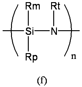
- n represents an arbitrary natural number.
- Rm, Rp, and Rt each independently represent a non-hydrolyzable group such as a hydrogen atom, an alkyl group, a cycloalkyl group, an alkenyl group, an aryl group, or an alkylsilyl group.
- alkyl group, alkenyl group, and aryl group are the same as those exemplified for Rx and the like.
- Examples of the cycloalkyl group are the same as those exemplified for Rq and the like.
- alkylsilyl group examples include a trimethylsilyl group, a triethylsilyl group, a triisopropylsilyl group, a tri-t-butylsilyl group, a methyldiethylsilyl group, a dimethylsilyl group, a diethylsilyl group, a methylsilyl group, and an ethylsilyl group.
- Rm, Rp, and Rt a hydrogen atom, an alkyl group having 1 to 6 carbon atoms, or a phenyl group is preferable, and a hydrogen atom is particularly preferable.
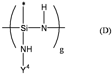
- Examples of the polysilazane compound having a repeating unit represented by the formula (f) include inorganic polysilazanes in which Rm, Rp, and Rt are all hydrogen atoms, and organic polysilazanes in which at least one of Rm, Rp, and Rt is not a hydrogen atom. It may be.
- inorganic polysilazane the following formula
- perhydropolysilazane having a linear structure, a branched structure and a cyclic structure in the molecule.
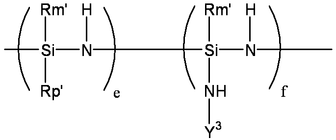
- organic polysilazane (I) — (Rm′SiHNH) — (Rm ′ represents the same alkyl group, cycloalkyl group, alkenyl group, aryl group or alkylsilyl group as Rm. The same applies to the following Rm ′).
- the organic polysilazane can be produced by a conventionally known method. For example, the following formula
- m represents 2 or 3
- X represents a halogen atom
- R 1 represents any of the substituents of Rm, Rp, Rt, Rm ′, Rp ′, and Rt ′ described above.
- the secondary amine, ammonia, and primary amine to be used may be appropriately selected according to the structure of the target polysilazane compound.
- a modified polysilazane compound can also be used as the polysilazane compound.
- the modified polysilazane include, for example, a polymetallosilazane containing a metal atom (the metal atom may be crosslinked), and repeating units of [(SiH 2 ) j (NH) h )] and [(SiH 2 ) i O] (wherein, j, h, i are each independently 1, 2 or 3.
- polysiloxazane JP 62-195024 discloses represented by)
- boron compound polysilazane Polyborosilazane produced by reacting polysilazane (Japanese Patent Laid-Open No.
- polymetallosilazane produced by reacting polysilazane and metal alkoxide Japanese Patent Laid-Open No. 63-81122, etc.
- inorganic silazane high polymer And modified polysilazanes such as JP-A-1-138108
- copolymerized silazanes obtained by introducing an organic component into polysilazane such as JP-A-2-175726
- Low-temperature ceramicized polysilazane Japanese Patent Laid-Open No.
- perhydropolysilazane with alcohol such as methanol or hexamethyldisilazane at the terminal N atom
- alcohol such as methanol or hexamethyldisilazane at the terminal N atom
- modified polysilazanes obtained by addition JP-A-5-345826, JP-A-4-63833
- inorganic polysilazane in which Rm, Rp, and Rt are all hydrogen atoms, and organic polysilazane in which at least one of Rm, Rp, and Rt is not a hydrogen atom are preferable and easily available. From the viewpoint of forming an injection layer having excellent gas barrier properties, inorganic polysilazane is more preferable.
- the polysilazane type compound can also use the commercial item marketed as a glass coating material etc. as it is.
- the low refractive layer may contain other components as long as the object of the present invention is not impaired.
- other components include a curing agent, an anti-aging agent, a light stabilizer, and a flame retardant.
- a polymer other than the silicon-based polymer may be included.
- the content of the silicon-based polymer compound in the low-refractive layer can efficiently form an intermediate refractive layer having desired characteristics by ion implantation such as plasma ion implantation described later.
- the reference is preferably 50% by mass or more, and more preferably 70% by mass or more.
- the low refractive layer can be formed by drying, and if necessary, heating and irradiating with energy rays.
- ion implantation treatment such as plasma ion implantation on the silicon polymer layer
- Part is modified to become an intermediate refractive layer, and the remaining portion is kept at low refractive index and becomes a low refractive layer.
- ion implantation processing such as plasma ion implantation on the silicon-based polymer layer, a low refractive layer having a predetermined thickness can be formed simultaneously with the intermediate refractive layer.
- Examples of the coating apparatus used when applying the low refractive layer forming solution include known apparatuses such as a spin coater, a knife coater, and a gravure coater.
- the coating film drying and heating method conventionally known drying methods such as hot air drying, hot roll drying, and infrared irradiation can be employed.
- the heating temperature is usually 80 to 150 ° C.
- the heating time is usually several tens of seconds to several tens of minutes.
- the intermediate refractive layer used in the present invention is a layer having a refractive index of 1.50 to 1.80, preferably 1.55 to 1.75, more preferably 1.60 to 1.70.
- a transparent conductive laminate excellent in optical characteristics (total light transmittance and color tone) and heat resistance can be obtained. If the refractive index is less than 1.50, the intermediate refractive layer is not preferable because the heat and humidity resistance decreases. On the other hand, if the refractive index is greater than 1.80, the optical properties and heat resistance are lowered, which is not preferable.
- the intermediate refractive layer used in the present invention is a layer having a film density of 2.5 to 4.5 g / cm 3 , preferably 2.7 to 3.5 g / cm 3 .
- an intermediate refractive layer having a film density of less than 2.5 is used, the moisture and heat resistance of the transparent conductive laminate decreases. Also, if the film density exceeds 4.5, the flexibility of the intermediate refractive layer is reduced, cracks may occur during the production process of the transparent conductive laminate or during transportation, and the heat and moisture resistance may deteriorate. is there.
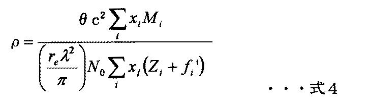
- the film density can be calculated using an X-ray reflectivity method (XRR). X-rays are totally reflected when they are incident on the thin film on the substrate at a very shallow angle. When the angle of incident X-rays exceeds the total reflection critical angle, X-rays enter the thin film and are divided into transmitted waves and reflected waves at the thin film surface and interface, and the reflected waves interfere. By analyzing the total reflection critical angle, the density of the film can be obtained. Note that the thickness of the thin film can also be obtained from measurement while changing the incident angle and analyzing the interference signal of the reflected wave accompanying the change in the optical path difference.
- the film density can be measured by the following method. In general, it is known that the refractive index n of a substance with respect to X-rays and ⁇ of the real part of the refractive index n are expressed by the following equations 1 and 2.
- the r e is the electron classical radius (2.818 ⁇ 10 -15 m)
- N 0 is the Avogadro's number
- a wavelength of ⁇ is X-ray
- [rho is the density (g / cm 3)
- Zi , Mi and xi represent the atomic number, atomic weight and atomic number ratio (molar ratio) of the i-th atom, respectively
- fi ′ represents the atomic scattering factor (anomalous dispersion term) of the i-th atom.
- the total reflection critical angle ⁇ c is given by Equation 3 when ⁇ related to absorption is ignored.
- ⁇ c 2 is a value that can be obtained from the X-ray reflectivity
- r e , N 0 , and ⁇ are constants
- Zi, Mi, and fi ′ are values specific to the constituent atoms.
- xi atomic number ratio (molar ratio)
- the film density in the intermediate refractive layer is measured by the method described in Examples and is obtained by using Equation 4.
- the intermediate refractive layer has an optical film thickness of usually 1 to 100 nm, preferably 10 to 50 nm. When the optical film thickness of the intermediate refractive layer is within this range, a thin transparent conductive laminate having excellent optical characteristics can be obtained.
- the intermediate refraction layer has the above characteristics, its constituent components and formation method are not particularly limited, and known ones can be used.
- the material for the intermediate refractive layer include oxides such as aluminum oxide, magnesium oxide, and silicon oxide; nitrides such as silicon nitride; oxynitrides such as silicon oxynitride; and the like. Of these, those containing an oxygen atom and a silicon atom are preferred. When the intermediate refractive layer contains oxygen atoms and silicon atoms, an intermediate refractive layer having excellent gas barrier properties can be easily formed.
- the presence ratio of each atom to the total amount of oxygen atoms, silicon atoms, and oxygen atoms is preferably 60 to 75 oxygen atoms. %, Silicon atoms are 25 to 35%, and nitrogen atoms are 0 to 10%.
- the intermediate refractive layer for example, it may be directly formed by a physical or chemical deposition method such as an evaporation method, a sputtering method, an ion plating method, a thermal CVD method, a plasma CVD method, A method of forming a layer having a specific chemical composition by ion implantation or the like may be used.
- a method of performing plasma ion implantation treatment is preferable because the intermediate refractive layer can be easily formed.
- the intermediate refractive layer having the above characteristics can be easily formed by subjecting the silicon-based polymer layer to plasma ion implantation. Specifically, by applying plasma ion implantation treatment to the silicon-based polymer layer used as the low refractive layer, an intermediate refractive layer having the above characteristics is formed by modifying a part (surface layer portion) thereof. can do.
- the ion implantation region is changed by changing the ion implantation voltage, and thereby the refractive index of the intermediate refractive layer is changed. Can be controlled.
- an intermediate refractive layer having a target refractive index can be easily formed.
- ions to be implanted ions of rare gases such as argon, helium, neon, krypton, and xenon; ions such as fluorocarbon, hydrogen, nitrogen, oxygen, carbon dioxide, chlorine, fluorine, and sulfur; Ions of alkane gases such as methane, ethane, propane, butane, pentane and hexane; ions of alkene gases such as ethylene, propylene, butene and pentene; ions of alkadiene gases such as pentadiene and butadiene; acetylene, Ions of alkyne gases such as methylacetylene; ions of aromatic hydrocarbon gases such as benzene, toluene, xylene, indene, naphthalene and phenanthrene; ions of cycloalkane gases such as cyclopropane and cyclohexane; cyclopentene, Ions of cycloalkene gases
- organosilicon compound examples include tetraalkoxysilanes such as tetramethoxysilane, tetraethoxysilane, tetra n-propoxysilane, tetraisopropoxysilane, tetra n-butoxysilane, and tetra t-butoxysilane;
- An alkylalkoxysilane having an unsubstituted or substituted group such as dimethyldimethoxysilane, dimethyldiethoxysilane, diethyldimethoxysilane, methyltriethoxysilane, ethyltrimethoxysilane, (3,3,3-trifluoropropyl) trimethoxysilane;
- Arylalkoxysilanes such as diphenyldimethoxysilane and phenyltriethoxysilane;
- Disiloxanes such as hexamethyldisiloxane (H
- hydrogen, nitrogen, oxygen, argon, helium, neon can be formed more easily because it can form an intermediate refractive layer having particularly excellent gas barrier properties and desired optical characteristics.
- At least one ion selected from the group consisting of xenon and krypton is preferred.
- the method of implanting ions is not particularly limited, and examples thereof include a method of irradiating ions accelerated by an electric field (ion beam), a method of implanting ions in plasma, and the like. Among them, in the present invention, the latter method of implanting plasma ions is preferable because an intermediate refractive layer having desired characteristics can be easily formed.
- a method of injecting ions existing in plasma generated using an external electric field into the surface portion of the silicon-based polymer layer, or (B) without using an external electric field A method of injecting ions present in plasma generated only by an electric field by a negative high voltage pulse applied to the layer into the surface portion of the silicon-based polymer layer is preferable.
- the pressure during ion implantation is preferably 0.01 to 1 Pa.
- the pressure at the time of plasma ion implantation is within such a range, ions can be implanted easily and efficiently uniformly, and the target intermediate refractive layer can be efficiently formed.
- the processing operation is simple, and the processing time can be greatly shortened. Further, the entire layer can be processed uniformly, and ions in the plasma can be continuously injected into the surface portion of the layer with high energy when a negative high voltage pulse is applied. Furthermore, without applying special other means such as radio frequency (hereinafter abbreviated as “RF”) or a high frequency power source such as a microwave, just applying a negative high voltage pulse to the layer, A high-quality ion-implanted layer can be uniformly formed on the surface of the layer.
- RF radio frequency
- a high frequency power source such as a microwave
- the pulse width when applying a negative high voltage pulse is preferably 1 to 15 ⁇ sec.
- the pulse width is in such a range, ions can be implanted more easily and efficiently and uniformly.
- the applied voltage when generating plasma is preferably -1 to -50 kV, more preferably -1 to -30 kV, and particularly preferably -5 to -20 kV. If ion implantation is performed at an applied voltage greater than ⁇ 1 kV, the ion implantation amount (dose amount) becomes insufficient, and desired performance cannot be obtained. On the other hand, if ion implantation is performed at a value smaller than ⁇ 50 kV, the film is charged at the time of ion implantation, and problems such as coloring of the film occur, which is not preferable.
- Examples of the ion species to be plasma ion implanted include those exemplified as the ions to be implanted.
- a plasma ion implantation apparatus When ions in plasma are implanted into the surface portion of the layer, a plasma ion implantation apparatus is used. Specifically, as a plasma ion implantation apparatus, ( ⁇ ) high-frequency power is applied to a feedthrough that applies a negative high-voltage pulse to a silicon-based polymer layer (hereinafter also referred to as “ion-implanted layer”). An apparatus for surrounding the layer to be ion-implanted in a uniform manner with plasma uniformly, attracting, implanting, colliding and depositing ions in the plasma (Japanese Patent Laid-Open No.
- a plasma ion implantation apparatus that generates plasma using an external electric field such as a high-frequency power source such as a microwave, and attracts and injects ions in the plasma by applying a high-voltage pulse
- a plasma ion implantation apparatus that implants ions in plasma generated only by an electric field generated by applying a high voltage pulse without using an external electric field.
- the plasma ion implantation apparatus ( ⁇ ) or ( ⁇ ) because the processing operation is simple, the processing time can be greatly shortened, and it is suitable for continuous use.
- Examples of the method using the plasma ion implantation apparatus ( ⁇ ) and ( ⁇ ) include those described in International Publication WO2010 / 021326.
- the plasma generating means for generating plasma is also used by the high voltage pulse power source, other special means such as a high frequency power source such as RF and microwave are used.
- a high frequency power source such as RF and microwave.
- a portion that has been modified by ion implantation in the surface portion by generating a plasma simply by applying a negative high-voltage pulse without the need to inject ions in the plasma continuously into the surface portion of the polymer layer. It is possible to mass-produce a film in which a silicon-based polymer layer having a thickness, that is, an intermediate refractive layer is formed.
- the ion implantation can be confirmed by performing an elemental analysis measurement in the vicinity of 10 nm from the surface of the polymer layer using X-ray photoelectron spectroscopy (XPS).
- XPS X-ray photoelectron spectroscopy
- the transparent conductive layer used in the present invention is a transparent thin film layer having conductivity.
- the transparent conductive layer generally has an optical film thickness of 10 to 300 nm, preferably 10 to 250 nm, more preferably 50 to 250 nm, and still more preferably 100 to 200 nm. When the optical film thickness of the transparent conductive layer is within this range, a thin transparent conductive laminate having excellent optical characteristics can be obtained.
- a transparent conductive layer As a transparent conductive layer, a conventionally well-known thing can be used as a transparent conductive layer of an electronic member or an optical member.
- the material constituting the transparent conductive layer include metals, alloys, metal oxides, electrically conductive compounds, and mixtures thereof.
- Zinc oxide, zinc oxide doped with gallium (GZO), and aluminum are used to reduce the amount of rare metal used and to design an environment-friendly product.
- Zinc oxide-based conductive materials such as doped zinc oxide (AZO) and zinc indium oxide (IZO) are more preferable, and in view of durability and material cost, zinc oxide doped with gallium (GZO) is more preferable and conductive.
- zinc oxide to which digallium trioxide is added in an amount of 1 to 10% is particularly preferable.
- the transparent conductive layer may be formed by laminating a plurality of layers made of these materials.
- Examples of the method for forming the transparent conductive layer include vapor deposition, sputtering, ion plating, thermal CVD, and plasma CVD. Among these, in the present invention, the sputtering method is preferable because the conductor layer can be easily formed.
- the sputtering method introduces a discharge gas (such as argon) into a vacuum chamber, applies a high-frequency voltage or a direct current voltage between the target and the substrate to turn the discharge gas into plasma, and collides the plasma with the target material.
- a discharge gas such as argon
- This is a method of obtaining a thin film by skipping and attaching to a substrate.
- a target made of a material for forming the transparent conductive layer is used as the target.
- the low refractive layer, the intermediate refractive layer, and the transparent conductive layer are formed on at least one surface of the base material directly or via one or more layers in order from the base material side. Are laminated.
- the transparent conductive laminate of the present invention may have layers other than these layers.
- Examples of such a layer include an undercoat layer between the base material and the low refractive layer. By providing the undercoat layer, a transparent conductive laminate having excellent adhesion between the substrate and the low refractive layer can be easily obtained.
- the material constituting the undercoat layer is not particularly limited, and known materials can be used.
- a silicon-containing compound a photopolymerizable composition containing a photopolymerizable monomer and / or a photopolymerizable prepolymer, and a photopolymerization initiator; a polyester-based resin, a polyurethane-based resin (particularly a polyacryl polyol) , Polyester polyols, polyether polyols and isocyanate compounds and two-component curable resins), acrylic resins, polycarbonate resins, vinyl chloride / vinyl acetate copolymers, polyvinyl butyral resins, nitrocellulose resins, etc. Alkyl titanate; ethyleneimine; and the like. These materials can be used alone or in combination of two or more.
- the undercoat layer is formed by applying a solution for forming an undercoat layer obtained by dissolving or dispersing the above materials in an appropriate solvent on one side of the substrate, drying the obtained coating film, and, if desired, energy rays. Can be formed by irradiation.
- a normal wet coating method can be used as a method for applying the undercoat layer forming solution to the substrate. Examples include dipping method, roll coating, gravure coating, knife coating, air knife coating, roll knife coating, die coating, screen printing method, spray coating, gravure offset method and the like.
- drying the coating film of the solution for forming the undercoat layer conventionally known drying methods such as hot air drying, hot roll drying, and infrared irradiation can be employed.
- the irradiated energy rays energy rays generated from various energy ray generators are used.
- ultraviolet rays radiated from an ultraviolet lamp are usually used.
- an ultraviolet lamp such as a high-pressure mercury lamp, a fusion H lamp, or a xenon lamp that emits ultraviolet light having a spectral distribution in a wavelength range of 300 to 400 nm is usually used, and the irradiation amount is usually 50 to 3000 mJ / cm 2 is preferred.
- the thickness of the undercoat layer is preferably in the range of 0.05 to 20 ⁇ m, more preferably 0.1 to 10 ⁇ m, and still more preferably 0.5 to 5 ⁇ m.
- the refractive index of the undercoat layer is usually 1.4 to 1.7, preferably 1.4 to 1.6. When the refractive index of the undercoat layer is within the above range, it is possible to easily obtain a transparent conductive laminate having excellent transparency, suppressing yellowness and excellent optical characteristics.
- the transparent conductive laminate of the present invention has a low surface resistivity.
- the surface resistivity is preferably 1000 ⁇ / ⁇ or less, and more preferably 100 to 600 ⁇ / ⁇ . By being within such a range, a transparent conductive laminate suitable for a capacitive touch panel can be obtained.
- the transparent conductive laminate of the present invention is excellent in heat and moisture resistance. This can be confirmed from the fact that the change in surface resistivity is small when the transparent conductive laminate of the present invention is placed under wet heat conditions. That is, the surface resistivity of the transparent conductive laminate after being stored for 7 days at R 0 , 60 ° C. and 90% RH (relative humidity) is R. When 1 ,
- T is preferably less than 1.5, and more preferably 1.0 or more and less than 1.2.
- the surface resistivity of the transparent conductive laminate can be measured by a known method (for example, a four-terminal four-probe constant current application method).
- the transparent conductive laminate of the present invention is excellent in moisture and heat resistance because the laminate immediately after forming the intermediate refractive layer used in the production of the transparent conductive laminate of the present invention (in the state before providing the transparent conductive layer) ) Can be confirmed from the fact that the permeability of gas such as water vapor is very small.
- the water vapor permeability of the laminate, 40 ° C., under a relative humidity of 90% is preferably from 0.1g / m 2 / day, more preferably 0.001 ⁇ 0.05g / m 2 / day .
- the transparent conductive laminate of the present invention also has a low permeability of gas such as water vapor.
- the transparent conductive moisture vapor transmission rate of the laminate of the present invention is preferably from 0.1g / m 2 / day, 0.001 ⁇ 0.05g / m 2 / Day is more preferable.
- the water vapor transmission rate can be measured using a known gas transmission rate measuring device.
- the transparent conductive laminate of the present invention is excellent in transparency. This can be confirmed from the high total light transmittance of the transparent conductive laminate of the present invention.
- the total light transmittance is preferably 80% or more, more preferably 80 to 95%, and still more preferably 85 to 90%.
- the total light transmittance can be measured using a known visible light transmittance measuring device.
- the transparent conductive laminate of the present invention has a natural color tone with suppressed yellowness. This can be confirmed from the fact that the absolute value of the transmission hue b * value of the transparent conductive laminate of the present invention is small.
- the transmitted hue b * value is preferably ⁇ 2.0 to +2.0, more preferably ⁇ 1.5 to +1.5, and even more preferably ⁇ 1.0 to +1.0.
- the transparent conductive laminate of the present invention Since the transparent conductive laminate of the present invention has the above properties, it is suitable as an electronic member such as an electrode used in an electronic device or module such as an image display device such as a liquid crystal display, an electroluminescence (EL) display, and a touch panel. is there.
- an electronic member such as an electrode used in an electronic device or module such as an image display device such as a liquid crystal display, an electroluminescence (EL) display, and a touch panel. is there.
- the film density of the intermediate refractive layer was calculated from the X-ray reflectivity measured under the measurement conditions shown below to determine the total reflection critical angle ⁇ c.
- the measuring apparatus and measurement conditions are as follows.
- Measuring apparatus Sample horizontal X-ray diffractometer for thin film evaluation “SmartLab” manufactured by Rigaku Corporation Measurement conditions: X-ray source: Cu-K ⁇ 1 (wavelength: 1.54059 mm)
- Optical system Parallel beam optical system Incident side slit system: Ge (220) 2 crystal, height limiting slit 5 mm, incident slit 0.05 mm
- Receiving side slit system receiving slit 0.10mm, solar slit 5 ° Detector; Scintillation counter Tube voltage and tube current; 45kV-200mA Scanning axis; 2 ⁇ / ⁇ Scan mode; continuous scan scan range; 0.1-3.0 deg. Scanning speed: 1 deg.
- the water vapor transmission rate was measured under the conditions of a relative humidity of 90% and a temperature of 40 ° C. using PERMATRAN-W3 / 33 manufactured by mocon.
- the surface resistivity of the transparent conductive laminate was measured by using a device “LORESTA-GP MCP-T600” manufactured by Mitsubishi Chemical Corporation (probe: “PROBE TYPE ASP” manufactured by Mitsubishi Chemical Analytech Co., Ltd.) with a relative humidity of 50% and a temperature. The measurement was performed at 23 ° C.
- the total light transmittance of the transparent conductive laminate was measured according to JIS K 7631-1 using a turbidimeter (manufactured by Nippon Denshoku Industries Co., Ltd., HAZE METER NDH5000).
- Y and Z are tristimulus values in the XYZ coordinate system of the sample measured with a color difference meter, and Yn and Zn are tristimulus values on a completely diffuse reflecting surface.
- the increase rate T of the surface resistivity represented by is calculated, and the heat and humidity resistance was evaluated according to the following criteria. ⁇ ⁇ ⁇ ⁇ T is less than 1.2 ⁇ ⁇ ⁇ ⁇ T is 1.2 or more and less than 1.5 ⁇ ⁇ ⁇ ⁇ T is 1.5 or more
- the total light transmittance and the transmitted hue b * value were measured by the above method, and the optical characteristics were evaluated according to the following criteria.
- the absolute value of the value is 1.0 or less, or the total light transmittance is 85% or more, and the absolute value of the transmitted hue b * value is more than 1.0 and 2.0 or less. Or the absolute value of the transmitted hue b * value is over 2.0.
- the solution was neutralized with a saturated aqueous sodium hydrogen carbonate solution, the aqueous layer was removed, and the resulting organic layer was dried over magnesium sulfate. After magnesium sulfate was filtered off, the filtrate was concentrated under reduced pressure and purified by reprecipitation using n-hexane. After the purified product was dissolved in ethyl acetate, 2,4,6-trimethylbenzoyl-diphenyl-phosphine oxide (manufactured by BASF Corp., Lucirin (registered trademark) TPO) was used as a photopolymerization initiator with respect to the solid content. 2 wt% of 1% by weight, 1-hydroxy-cyclohexyl-phenyl-ketone was added to the solid content to obtain an undercoat layer forming solution.
- 2,4,6-trimethylbenzoyl-diphenyl-phosphine oxide manufactured by BASF Corp., Lucirin (registered trademark) TPO
- Example 1 The undercoat layer forming solution obtained in Production Example 1 was applied onto a polyester film (Toyobo Co., Ltd., Cosmo Shine PETA4300, thickness 100 ⁇ m), dried by heating at 120 ° C. for 1 minute, and then using a UV light irradiation line. UV light irradiation (high pressure mercury lamp, line speed, 20 m / min, integrated light quantity 100 mJ, peak intensity 1.466 W, number of passes twice), undercoat layer (thickness 1100 nm, refractive index 1.49, optical film thickness 1639 nm) Formed.
- UV light irradiation high pressure mercury lamp, line speed, 20 m / min, integrated light quantity 100 mJ, peak intensity 1.466 W, number of passes twice
- undercoat layer thickness 1100 nm, refractive index 1.49, optical film thickness 1639 nm
- a perhydropolysilazane solution (Aquamica NL110A-20) is applied on the undercoat layer, dried by heating at 120 ° C. for 1 minute, and a silicon-based polymer layer (thickness 150 nm, refractive index 1.45, optical thickness 218 nm) Formed.
- Ar is plasma-implanted into the surface of the silicon-based polymer layer to modify a part of the silicon-based polymer layer, so that the intermediate refractive layer (surface layer portion) ) And a low refractive layer (unmodified part).
- the obtained low refractive layer has a thickness of 120 nm, a refractive index of 1.45, an optical film thickness of 170 nm, and the intermediate refractive layer has a film density of 2.76 g / cm 3 , a thickness of 30 nm, a refractive index of 1.59, and an optical film thickness of 48 nm. there were.
- the plasma ion implantation apparatus and plasma-on implantation conditions used are as follows.
- RF power source JEOL Ltd., model number “RF” 56000
- High voltage pulse power supply “PV-3-HSHV-0835” manufactured by Kurita Manufacturing Co., Ltd.
- Plasma generation gas Ar Gas flow rate: 100sccm Duty ratio: 0.5% Repeat frequency: 1000Hz Applied voltage: -6kV RF power supply: frequency 13.56 MHz, applied power 1000 W Chamber internal pressure: 0.2 Pa
- Pulse width 5 ⁇ sec Processing time (ion implantation time): 5 minutes Conveying speed: 0.2 m / min
- a transparent conductive layer (thickness 92 nm, refractive index 1.81, optical thickness 167 nm) using a zinc oxide target material containing 5.7% by mass of Ga 2 O 3 by DC magnetron sputtering. ) To form a transparent conductive laminate 1.
- the characteristics and evaluation results of the transparent conductive laminate 1 are shown in Table 1.
- a transparent conductive layer was formed under the following conditions.
- Substrate temperature Room temperature DC output: 500W
- Carrier gas Argon
- the water-vapor transmission rate was 0.01 g / m ⁇ 2 > / day or less.
- Example 2 A transparent conductive laminate 2 was produced in the same manner as in Example 1 except that a transparent conductive layer having a thickness of 110 nm, a refractive index of 1.81, and an optical film thickness of 199 nm was formed in Example 1.
- Table 1 shows the characteristics and evaluation results of the transparent conductive laminate 2.
- Example 3 In Example 1, the applied voltage in ion implantation is ⁇ 10 kV, the thickness is 100 nm, the refractive index is 1.45, the low refractive layer has an optical film thickness of 145 nm, the film density is 3.32 g / cm 3 , the thickness is 35 nm, and the refractive index is 1.66.
- a transparent conductive laminate 3 was produced in the same manner as in Example 1 except that an intermediate refractive layer having an optical film thickness of 58 nm was formed. The characteristics and evaluation results of the transparent conductive laminate 3 are shown in Table 1. In addition, in the state which does not provide a transparent conductive layer, the water-vapor transmission rate was 0.01 g / m ⁇ 2 > / day or less.
- Example 4 A transparent conductive laminate 4 was produced in the same manner as in Example 3 except that a transparent conductive layer having a thickness of 110 nm, a refractive index of 1.81, and an optical film thickness of 199 nm was formed in Example 3. The characteristics and evaluation results of the transparent conductive laminate 4 are shown in Table 1.
- Example 5 In Example 1, an applied voltage in ion implantation is set to ⁇ 15 kV, a low refractive layer having a thickness of 100 nm, a refractive index of 1.45, an optical film thickness of 145 nm, a film density of 4.45 g / cm 3 , a thickness of 53 nm, and a refractive index of 1.78.
- a transparent conductive laminate 5 was produced in the same manner as in Example 1 except that an intermediate refractive layer having an optical thickness of 94 nm was formed. Table 1 shows the characteristics and evaluation results of the transparent conductive laminate 5.
- Example 6 In Example 1, an indium oxide target material (manufactured by Sumitomo Metal Mining Co., Ltd.) containing 10% by mass of SnO 2 was formed on the intermediate refractive layer by DC magnetron sputtering, and a transparent conductive layer (thickness 112 nm, refractive index) A transparent conductive laminate 6 was produced in the same manner as in Example 1 except that 2.00 and an optical film thickness of 224 nm were formed. The characteristics and evaluation results of the transparent conductive laminate 6 are shown in Table 1.
- Example 6 The conditions for forming the transparent conductive layer in Example 6 are as follows. Substrate temperature: Room temperature DC output: 500W Carrier gas: Argon + oxygen (oxygen flow ratio 2%)
- Comparative Example 1 A transparent conductive laminate 7 was produced in the same manner as in Example 1 except that plasma ion implantation was not performed in Example 1. Table 1 shows the characteristics and evaluation results of the transparent conductive laminate 7.
- a portion of 30 nm from the surface of the silicon-based polymer layer in contact with the transparent conductive layer toward the undercoat layer portion corresponding to the intermediate refractive layer in other examples is formally formed as a surface layer.
- Part (intermediate refractive layer), and other parts are formally determined as low refractive layers.
- Table 1 shows intermediate refractive layers (film density 2.2 g / cm 3 , thickness 30 nm, refractive index 1.45, optical film 44 nm) and a low refractive layer (refractive index 1.45, optical film thickness 218 nm).
- Table 1 shows the following.
- the transparent conductive laminates 1 to 6 of Examples 1 to 6 are all excellent in moisture and heat resistance, have a high total light transmittance, have a low absolute value of the transmitted hue b * value, and are suppressed in yellowness. Excellent optical properties.
- the transparent conductive laminate 7 of Comparative Example 1 the film density and refractive index of the intermediate refractive layer are too small. For this reason, the transparent conductive laminated body 7 is inferior in heat-and-moisture resistance, and the total light transmittance is also a low value of 80%.
Landscapes
- Engineering & Computer Science (AREA)
- Chemical & Material Sciences (AREA)
- Ceramic Engineering (AREA)
- Physics & Mathematics (AREA)
- Microelectronics & Electronic Packaging (AREA)
- Theoretical Computer Science (AREA)
- General Engineering & Computer Science (AREA)
- Structural Engineering (AREA)
- General Physics & Mathematics (AREA)
- Organic Chemistry (AREA)
- Manufacturing & Machinery (AREA)
- Materials Engineering (AREA)
- Human Computer Interaction (AREA)
- Nonlinear Science (AREA)
- Optics & Photonics (AREA)
- Crystallography & Structural Chemistry (AREA)
- Mathematical Physics (AREA)
- Laminated Bodies (AREA)
- Non-Insulated Conductors (AREA)
- Surface Treatment Of Optical Elements (AREA)
Abstract
Description
しかし、プラスチックフィルムは、ガラス板に比べて水蒸気や酸素等を透過しやすく、電子部材内部の素子の劣化を起こしやすいという問題があった。
(1)基材の少なくとも一方の面に、直接又は1層以上の層を介して、基材側から順に、低屈折層、中間屈折層、及び透明導電層を積層してなる透明導電性積層体であって、低屈折層の屈折率が1.40~1.50、中間屈折層の屈折率が1.50~1.80、かつ、中間屈折層の膜密度が2.5~4.5g/cm3であることを特徴とする透明導電性積層体。
(2)前記中間屈折層の光学膜厚が1~100nmである、(1)に記載の透明導電性積層体。
(3)前記低屈折層の光学膜厚が10~800nmである、(1)に記載の透明導電性積層体。
(4)前記透明導電層の光学膜厚が10~250nmである、(1)に記載の透明導電性積層体。
(5)40℃、相対湿度90%雰囲気下での水蒸気透過率が0.1g/m2/day以下である、(1)に記載の透明導電性積層体。
(6)透過色相b*値が-2.0~+2.0、かつ、全光線透過率が80%以上である、(1)に記載の透明導電性積層体。
(7)前記透明導電層を構成する材料が、酸化亜鉛、ガリウムをドープした酸化亜鉛(GZO)、アルミニウムをドープした酸化亜鉛(AZO)及び酸化亜鉛インジウム(IZO)からなる群から選ばれる少なくとも1種である、(1)に記載の透明導電性積層体。
(8)前記中間屈折層及び低屈折層が、ケイ素系高分子層にイオン注入処理を施すことで得られる層である、(1)に記載の透明導電性積層体。
(7)前記(1)~(6)のいずれかに記載の透明導電性積層体を用いた電子デバイス又はモジュール。
本発明の電子デバイス又はモジュールは、本発明の透明導電性積層体を用いるものであるため、耐湿熱性に優れるとともに、黄色味が抑えられ、光学特性も優れるものである。
本発明に用いる基材は、無色透明なものであって、透明導電性積層体の基材として十分な強度を有するものであれば特に制限されない。
基材の材質としては、ポリイミド、ポリアミド、ポリアミドイミド、ポリフェニレンエーテル、ポリエーテルケトン、ポリエーテルエーテルケトン、ポリオレフィン、ポリエステル、ポリカーボネート、ポリスルフォン、ポリエーテルスルフォン、ポリフェニレンスルフィド、ポリアリレート、アクリル系樹脂、シクロオレフィン系ポリマー、芳香族系重合体、ポリウレタン系ポリマー等が挙げられる。
ポリエステルとしては、ポリエチレンテレフタレート、ポリブチレンテレフタレート、ポリエチレンナフタレート、ポリアリレート等が挙げられる。
ポリアミドとしては、全芳香族ポリアミド、ナイロン6、ナイロン66、ナイロン共重合体等が挙げられる。
シクロオレフィン系ポリマーとしては、ノルボルネン系重合体、単環の環状オレフィン系重合体、環状共役ジエン系重合体、ビニル脂環式炭化水素重合体、及びこれらの水素化物が挙げられる。その具体例としては、アペル(三井化学社製のエチレン-シクロオレフィン共重合体)、アートン(JSR社製のノルボルネン系重合体)、ゼオノア(日本ゼオン社製のノルボルネン系重合体)等が挙げられる。
これらの中でも、汎用性及びコストの観点から、ポリエチレンテレフタレート、ポリブチレンテレフタレート、ポリエチレンナフタレート、ポリアリレート等のポリエステルが好ましく、ポリエチレンテレフタレートがより好ましい。
基材の厚みは、通常0.01~0.5mm、好ましくは0.05~0.25mmである。基材の厚みがこの範囲内であることで、透明性及び屈曲性に優れる透明導電性積層体を容易に得ることができる。
また、基材の屈折率は、材質、延伸の有無によって異なるが、透明性の観点から、通常、1.45~1.75、好ましくは1.6~1.75の範囲である。
本発明の透明導電性積層体に用いる低屈折層は、屈折率が1.40~1.50、好ましくは、1.42~1.48の層である。本発明においては、かかる特性を有する低屈折層を、後述する中間屈折層と組み合わせて用いることで、光学特性(全光線透過率及び色調)に優れる透明導電性積層体を得ることができる。
低屈折層は、光学膜厚が、通常、10~800nm、好ましくは、100~500nmである。低屈折層の光学膜厚がこの範囲内であることで、光学特性に優れ、かつ、薄い透明導電性積層体を得ることができる。光学膜厚とは、層の屈折率(n)と層の膜厚(d)との積(n×d)をいう。
例えば、前記直鎖状の主鎖構造としては下記式(a)で表される構造が、ラダー状の主鎖構造としては下記式(b)で表される構造が、籠状の主鎖構造としては、例えば下記式(c)で表される構造が、それぞれ挙げられる。


1価の複素環基の具体例としては、2-ピリジル基、3-ピリジル基、4-ピリジル基、2-チエニル基、3-チエニル基、2-フリル基、3-フリル基、3-ピラゾリル基、4-ピラゾリル基、2-イミダゾリル基、4-イミダゾリル基、1,2,4-トリアジン-3-イル基、1,2,4-トリアジン-5-イル基、2-ピリミジル基、4-ピリミジル基、5-ピリミジル基、3-ピリダジル基、4-ピリダジル基、2-ピラジル基、2-(1,3,5-トリアジル)基、3-(1,2,4-トリアジル)基、6-(1,2,4-トリアジル)基、2-チアゾリル基、5-チアゾリル基、3-イソチアゾリル基、5-イソチアゾリル基、2-(1,3,4-チアジアゾリル)基、3-(1,2,4-チアジアゾリル)基、2-オキサゾリル基、4-オキサゾリル基、3-イソオキサゾリル基、5-イソオキサゾリル基、2-(1,3,4-オキサジアゾリル)基、3-(1,2,4-オキサジアゾリル)基、5-(1,2,3-オキサジアゾリル)基等が挙げられる。
Rのアルキレン基としては、メチレン基、エチレン基、プロピレン基、トリメチレン基、テトラメチレン基、ペンタメチレン基、ヘキサメチレン基、オクタメチレン基等の炭素数1~10のアルキレン基が挙げられる。

シクロアルケニル基としては、シクロペンテニル基、シクロヘキセニル基等の炭素数4~10のシクロアルケニル基が挙げられる。
シクロアルキルオキシ基としては、シクロペンチルオキシ基、シクロヘキシルオキシ基等の炭素数3~10のシクロアルキルオキシ基が挙げられる。
アラルキルオキシ基としては、ベンジルオキシ基、フェネチルオキシ基、フェニルプロピルオキシ基等の炭素数7~20のアラルキルオキシ基が挙げられる。
置換基を有していてもよいアミノ基としては、アミノ基;アルキル基、シクロアルキル基、アリール基、アラルキル基、アシル基等で置換されたN-モノ又はN,N-ジ置換アミノ基等が挙げられる。
ハロゲン原子としては、フッ素原子、塩素原子、臭素原子、ヨウ素原子等が挙げられる。
ポリシラン系化合物が非環状ポリシランである場合は、ポリシラン系化合物の末端基(末端置換基)は、水素原子であっても、ハロゲン原子(塩素原子等)、アルキル基、ヒドロキシル基、アルコキシ基、シリル基等であってもよい。
また、ポリシラン系化合物の重量平均分子量は、300~100,000、好ましくは400~50,000、さらに好ましくは500~30,000程度である。
Rm、Rp、Rtは、それぞれ独立して、水素原子、アルキル基、シクロアルキル基、アルケニル基、アリール基又はアルキルシリル基等の非加水分解性基を表す。
シクロアルキル基としては、前記Rq等で例示したのと同様のものが挙げられる。
無機ポリシラザンとしては、下記式


(i)-(Rm’SiHNH)-(Rm’は、Rmと同様のアルキル基、シクロアルキル基、アルケニル基、アリール基又はアルキルシリル基を表す。以下のRm’も同様である。)を繰り返し単位として、主として重合度が3~5の環状構造を有するもの、
(ii)-(Rm’SiHNRt’)-(Rt’は、Rtと同様のアルキル基、シクロアルキル基、アルケニル基、アリール基又はアルキルシリル基を表す。)を繰り返し単位として、主として重合度が3~5の環状構造を有するもの、
(iii)-(Rm’Rp’SiNH)-(Rp’は、Rpと同様のアルキル基、シクロアルキル基、アルケニル基、アリール基アルキルシリル基を表す。)を繰り返し単位として、主として重合度が3~5の環状構造を有するもの、
(iv)下記式で表される構造を分子内に有するポリオルガノ(ヒドロ)シラザン、

で表される繰り返し構造を有するポリシラザン等が挙げられる。
用いる2級アミン、アンモニア及び1級アミンは、目的とするポリシラザン系化合物の構造に応じて、適宜選択すればよい。
ケイ素アルコキシド付加ポリシラザン(特開平5-238827号公報)、グリシドール付加ポリシラザン(特開平6-122852号公報)、アセチルアセトナト錯体付加ポリシラザン(特開平6-306329号公報)、金属カルボン酸塩付加ポリシラザン(特開平6-299118号公報等)、
上記ポリシラザン又はその変性物に、アミン類及び/又は酸類を添加してなるポリシラザン組成物(特開平9-31333号公報)、ペルヒドロポリシラザンにメタノール等のアルコール或いはヘキサメチルジシラザンを末端N原子に付加して得られる変性ポリシラザン(特開平5-345826号公報、特開平4-63833号公報)等が挙げられる。
なお、ポリシラザン系化合物は、ガラスコーティング材等として市販されている市販品をそのまま使用することもできる。
低屈折層が、前記ケイ素系高分子層の場合、これらの成分に加えて、ケイ素系高分子以外の高分子を含んでいてもよい。低屈折層中のケイ素系高分子化合物の含有量は、後述するプラズマイオン注入等のイオン注入処理によって、目的の特性を有する中間屈折層を効率よく形成することができることから、低屈折層全体を基準として50質量%以上であるのが好ましく、70質量%以上であるのがより好ましい。
また、後述するようにケイ素系高分子層にプラズマイオン注入等のイオン注入処理を施すことで中間屈折層及び低屈折層を形成する場合は、かかる処理によってケイ素系高分子層の一部(表層部)が改質されて中間屈折層になり、残りの部分は低屈折性が維持され、低屈折層となる。このように、ケイ素系高分子層にプラズマイオン注入等のイオン注入処理を施すことで、中間屈折層と同時に、所定の厚みを有する低屈折層を形成することができる。
本発明に用いる中間屈折層は、屈折率が1.50~1.80、好ましくは1.55~1.75、より好ましくは1.60~1.70の層である。かかる特性を有する中間屈折層を前記低屈折層と組み合わせて用いることで、光学特性(全光線透過率及び色調)及び耐熱性に優れる透明導電性積層体を得ることができる。中間屈折層は、屈折率が1.50未満であると、耐湿熱性が低下するため好ましくない。一方、屈折率が1.80より大きいと光学特性及び耐熱性が低下するため好ましくない。
X線は、基板上の薄膜に対して非常に浅い角度で入射させると全反射される。入射X線の角度が全反射臨界角以上になると、薄膜内部にX線が侵入し薄膜表面や界面で透過波と反射波に分かれ、反射波は干渉する。全反射臨界角を解析することで、膜の密度を求めることができる。なお、入射角度を変えながら測定を行い、光路差の変化に伴う反射波の干渉信号の解析から、薄膜の膜厚も求めることができる。
膜密度は、以下の方法で測定することができる。
一般に、X線に対する物質の屈折率n、及び屈折率nの実部部分のδは以下の式1及び式2となることが知られている。

中間屈折層における膜密度は、実施例において説明する方法で測定し、式4を用いて得られる。
酸素原子、ケイ素原子及び酸素原子の存在量全体に対するそれぞれの原子の存在割合(原子数割合)は、透明導電性積層体の耐湿熱性や光学特性の観点から、好ましくは、酸素原子が60~75%、ケイ素原子が25~35%、窒素原子が0~10%である。
具体的には、低屈折層として用いたケイ素系高分子層にプラズマイオン注入処理を施すことによって、その一部(表層部)が改質されることで、前記特性を有する中間屈折層を形成することができる。
プラズマイオン注入法を用いる場合、イオン注入電圧を変えることで、イオン注入領域を変化させ、これにより、中間屈折層の屈折率を制御することができる。このように、イオン注入法を用いることで、目的の屈折率を有する中間屈折層を容易に形成することができる。
メタン、エタン、プロパン、ブタン、ペンタン、ヘキサン等のアルカン系ガス類のイオン;エチレン、プロピレン、ブテン、ペンテン等のアルケン系ガス類のイオン;ペンタジエン、ブタジエン等のアルカジエン系ガス類のイオン;アセチレン、メチルアセチレン等のアルキン系ガス類のイオン;ベンゼン、トルエン、キシレン、インデン、ナフタレン、フェナントレン等の芳香族炭化水素系ガス類のイオン;シクロプロパン、シクロヘキサン等のシクロアルカン系ガス類のイオン;シクロペンテン、シクロヘキセン等のシクロアルケン系ガス類のイオン;
金、銀、銅、白金、ニッケル、パラジウム、クロム、チタン、モリブデン、ニオブ、タンタル、タングステン、アルミニウム等の導電性の金属のイオン;
シラン(SiH4)又は有機ケイ素化合物のイオン;等が挙げられる。
ジメチルジメトキシシラン、ジメチルジエトキシシラン、ジエチルジメトキシシラン、メチルトリエトキシシラン、エチルトリメトキシシラン、(3,3,3-トリフルオロプロピル)トリメトキシシラン等の無置換若しくは置換基を有するアルキルアルコキシシラン;
ジフェニルジメトキシシラン、フェニルトリエトキシシラン等のアリールアルコキシシラン;
ヘキサメチルジシロキサン(HMDSO)等のジシロキサン;
ビス(ジメチルアミノ)ジメチルシラン、ビス(ジメチルアミノ)メチルビニルシラン、ビス(エチルアミノ)ジメチルシラン、ジエチルアミノトリメチルシラン、ジメチルアミノジメチルシラン、テトラキスジメチルアミノシラン、トリス(ジメチルアミノ)シラン等のアミノシラン;
ヘキサメチルジシラザン、ヘキサメチルシクロトリシラザン、ヘプタメチルジシラザン、ノナメチルトリシラザン、オクタメチルシクロテトラシラザン、テトラメチルジシラザン等のシラザン;
テトライソシアナートシラン等のシアナートシラン;
トリエトキシフルオロシラン等のハロゲノシラン;
ジアリルジメチルシラン、アリルトリメチルシラン等のアルケニルシラン;
ジ-t-ブチルシラン、1,3-ジシラブタン、ビス(トリメチルシリル)メタン、テトラメチルシラン、トリス(トリメチルシリル)メタン、トリス(トリメチルシリル)シラン、ベンジルトリメチルシラン等の無置換若しくは置換基を有するアルキルシラン;
ビス(トリメチルシリル)アセチレン、トリメチルシリルアセチレン、1-(トリメチルシリル)-1-プロピン等のシリルアルキン;
1,4-ビストリメチルシリル-1,3-ブタジイン、シクロペンタジエニルトリメチルシラン等のシリルアルケン;
フェニルジメチルシラン、フェニルトリメチルシラン等のアリールアルキルシラン;
プロパルギルトリメチルシラン等のアルキニルアルキルシラン;
ビニルトリメチルシラン等のアルケニルアルキルシラン;
ヘキサメチルジシラン等のジシラン;
オクタメチルシクロテトラシロキサン、テトラメチルシクロテトラシロキサン、ヘキサメチルシクロテトラシロキサン等のシロキサン;
N,O-ビス(トリメチルシリル)アセトアミド;
ビス(トリメチルシリル)カルボジイミド;
等が挙げられる。
これらのイオンは、一種単独で、あるいは二種以上を組み合わせて用いてもよい。
プラズマイオン注入装置としては、具体的には、(α)ケイ素系高分子層(以下、「イオン注入する層」ということがある。)に負の高電圧パルスを印加するフィードスルーに高周波電力を重畳してイオン注入する層の周囲を均等にプラズマで囲み、プラズマ中のイオンを誘引、注入、衝突、堆積させる装置(特開2001-26887号公報)、(β)チャンバー内にアンテナを設け、高周波電力を与えてプラズマを発生させてイオン注入する層周囲にプラズマが到達後、イオン注入する層に正と負のパルスを交互に印加することで、正のパルスでプラズマ中の電子を誘引衝突させてイオン注入する層を加熱し、パルス定数を制御して温度制御を行いつつ、負のパルスを印加してプラズマ中のイオンを誘引、注入させる装置(特開2001-156013号公報)、(γ)マイクロ波等の高周波電力源等の外部電界を用いてプラズマを発生させ、高電圧パルスを印加してプラズマ中のイオンを誘引、注入させるプラズマイオン注入装置、(δ)外部電界を用いることなく高電圧パルスの印加により発生する電界のみで発生するプラズマ中のイオンを注入するプラズマイオン注入装置等が挙げられる。
前記(γ)及び(δ)のプラズマイオン注入装置を用いる方法については、国際公開WO2010/021326号公報に記載のものが挙げられる。
本発明に用いる透明導電層は、導電性を有する透明な薄膜層である。
透明導電層は、光学膜厚が、通常、10~300nm、好ましくは10~250nm、より好ましくは、50~250nm、さらに好ましくは100~200nmである。透明導電層の光学膜厚がこの範囲内であることで、光学特性に優れ、かつ薄い透明導電性積層体を得ることができる。
透明導電層を構成する材料としては、金属、合金、金属酸化物、電気伝導性化合物、これらの混合物等が挙げられる。具体的には、酸化スズ、アンチモンをドープした酸化スズ(ATO);フッ素をドープした酸化スズ(FTO)、酸化亜鉛、ガリウムをドープした酸化亜鉛(GZO)、アルミニウムをドープした酸化亜鉛(AZO)、酸化インジウム、酸化インジウムスズ(ITO)、酸化亜鉛インジウム(IZO)、等の導電性金属酸化物;金、銀、クロム、ニッケル等の金属;これら金属と導電性金属酸化物との混合物;ヨウ化銅、硫化銅等の無機導電性物質;ポリアニリン、ポリチオフェン、ポリピロール等の有機導電性材料;等が挙げられる。これらの中でも、導電性の観点から導電性金属酸化物が好ましく、レアメタルの使用量を抑え、環境に配慮した製品設計を行なう上では、酸化亜鉛、ガリウムをドープした酸化亜鉛(GZO)、アルミニウムをドープした酸化亜鉛(AZO)、酸化亜鉛インジウム(IZO)などの酸化亜鉛系導電性材料がより好ましく、耐久性と材料コストを鑑みて、ガリウムをドープした酸化亜鉛(GZO)がさらに好ましく、導電性を考慮すると、三酸化二ガリウムを1~10%の範囲で添加した酸化亜鉛が特に好ましい。
透明導電層は、これらの材料からなる層が複数積層されてなるものであってもよい。
本発明の透明導電性積層体は、前記基材の少なくとも一方の面に、直接又は1層以上の層を介して、基材側から順に、前記低屈折層、中間屈折層、及び透明導電層を積層してなるものである。
アンダーコート層を設けることで、基材と低屈折層との密着性に優れる透明導電性積層体を容易に得ることができる。
また、アンダーコート層の屈折率は、通常、1.4~1.7、好ましくは1.4~1.6である。アンダーコート層の屈折率が上記範囲内であれば、透明性に優れ、黄色味が抑えられ光学特性に優れる透明導電性積層体を容易に得ることができる。
すなわち、湿熱条件下に置かれる前の透明導電性積層体の表面抵抗率をR0、60℃90%RH(相対湿度)で7日間保管した後の透明導電性積層体の表面抵抗率をR1としたとき、下記式
透明導電性積層体の表面抵抗率は、公知の方法(例えば、四端子四探針方式の定電流印加法)により測定することができる。
例えば、この積層体の水蒸気透過率は、40℃、相対湿度90%雰囲気下で、0.1g/m2/day以下が好ましく、0.001~0.05g/m2/dayがより好ましい。
また、かかる特性を有する積層体を用いて透明導電性積層体を製造することから、本発明の透明導電性積層体もまた、水蒸気等のガスの透過率が小さいものである。例えば、本発明の透明導電性積層体の水蒸気透過率は、40℃、相対湿度90%雰囲気下で、0.1g/m2/day以下が好ましく、0.001~0.05g/m2/dayがより好ましい。
水蒸気透過率は、公知のガス透過率測定装置を使用して測定することができる。
全光線透過率は、公知の可視光透過率測定装置を使用して測定することができる。
X線光電子分光測定装置を用いて、下記に示す測定条件にて、中間屈折層(イオン注入されて得られた層)における酸素原子、窒素原子及びケイ素原子の存在割合の測定を行った。
測定装置:「PHI Quantera SXM」アルバックファイ社製
X線源:AlKα
X線ビーム径:100μm
電力値:25W
電圧:15kV
取り出し角度:45°
真空度:5.0×10⁻⁸Pa
中間屈折層の膜密度は、下記に示す測定条件にてX線の反射率を測定して全反射臨界角度θcを求め、その値から算出した。
測定装置:薄膜評価用試料水平型X線回折装置「SmartLab」株式会社リガク製
測定条件:
X線源;Cu-Kα1(波長:1.54059Å)
光学系;並行ビーム光学系
入射側スリット系;Ge(220)2結晶、高さ制限スリット5mm、入射スリット0.05mm
受光側スリット系;受光スリット 0.10mm、ソーラースリット 5°
検出器;シンチレーションカウンター
管電圧・管電流;45kV-200mA
走査軸;2θ/θ
走査モード;連続スキャン
走査範囲;0.1-3.0deg.
走査速度;1deg./min.
サンプリング間隔;0.002°/step
なお、原子数比(xi)は、X線光電子分光測定により得られた中間屈折層における酸素原子、窒素原子及びケイ素原子の存在割合を用いた。
各層の屈折率及び膜厚は、分光エリプソメーターM-2000U(J.A.ウーラム・ジャパン社製)を用いて測定した。
水蒸気透過率は、mocon社製、PERMATRAN-W3/33を用いて、相対湿度90%、温度40℃の条件で測定した。
透明導電性積層体の表面抵抗率は、三菱化学社製の装置「LORESTA―GP MCP-T600」(プローブ:三菱化学アナリテック社製「PROBE TYPE ASP」)を用いて、相対湿度50%、温度23℃の条件下で測定した。
透明導電性積層体の全光線透過率は、濁度計(日本電色工業社製、HAZE METER NDH5000)を用いて、JIS K 7631-1に準じて測定した。
分光色差計(日本電色工業社製、Spectro Color Meter SQ2000)を用いて、JIS K 7105に準拠しつつ、透明導電性積層体の透過色相b*値(CIE1976L*a*b*表色系におけるb*軸の値)を測定した。
なお、b*値は、それぞれ下記式にて求められる値である。
上記方法により、透明導電性積層体の表面抵抗率を測定し、初期値(R0)を得た。次いで、60℃90%RH(相対湿度)で7日間保管した後に、同様に透明導電性積層体の表面抵抗率を測定し、湿熱条件後の値(R1)を得た。下記式
◎・・・Tが、1.2未満
○・・・Tが、1.2以上1.5未満
×・・・Tが、1.5以上
上記方法により、全光線透過率と透過色相b*値を測定し、以下の基準で光学特性を評価した。
◎・・・全光線透過率が85%以上、かつ、透過色相b*値の絶対値が1.0以下
○・・・全光線透過率が80%以上85%未満、かつ、透過色相b*値の絶対値が1.0以下、又は全光線透過率が85%以上、かつ、透過色相b*値の絶対値が1.0超2.0以下
×・・・全光線透過率が80%未満、又は、透過色相b*値の絶対値が2.0超
トリメトキシメチルシラン(AZMAX社製)5.78g(42.5mmol)、3-メタクリロキシプロピルトリエトキシシラン(信越化学社製、KBM-503)1.77g(7.5mmol)を酢酸エチル50mlに溶解させ、蒸留水25mlを加えて撹拌した。次いで、触媒としてリン酸数滴を加え、そのまま室温で18時間撹拌した。
この溶液に、飽和炭酸水素ナトリウム水溶液を加えて中和した後、水層を除去し、得られた有機層を硫酸マグネシウムで乾燥した。硫酸マグネシウムをろ別した後、ろ液を減圧濃縮し、n-ヘキサンを用いて再沈殿法により精製した。
精製物を、酢酸エチルに溶解させた後、光重合性開始剤として、2,4,6-トリメチルベンゾイル-ジフェニル-ホスフィンオキシド(BASF社製、Lucirin(登録商標)TPO)を固形分に対し1質量%、1-ヒドロキシ-シクロヘキシル-フェニル-ケトンを固形分に対し2wt%添加してアンダーコート層形成用溶液を得た。
ポリエステルフィルム(東洋紡社製、コスモシャインPETA4300、厚み100μm)上に製造例1で得られたアンダーコート層形成用溶液を塗布し、120℃で1分間加熱乾燥した後、UV光照射ラインを用いてUV光照射を行ない(高圧水銀灯、ライン速度、20m/min、積算光量100mJ、ピーク強度1.466W、パス回数2回)、アンダーコート層(厚み1100nm、屈折率1.49、光学膜厚1639nm)を形成した。
次に、プラズマイオン注入装置を用いて、このケイ素系高分子層の表面に、Arをプラズマイオン注入して、ケイ素系高分子層の一部を改質することにより、中間屈折層(表層部)及び低屈折層(非改質部)を形成した。得られた低屈折層は、厚み120nm、屈折率1.45、光学膜厚170nm、中間屈折層は、膜密度2.76g/cm3、厚み30nm、屈折率1.59、光学膜厚48nmであった。
(プラズマイオン注入装置)
RF電源:日本電子社製、型番号「RF」56000
高電圧パルス電源:栗田製作所社製、「PV-3-HSHV-0835」
(プラズマイオン注入条件)
プラズマ生成ガス:Ar
ガス流量:100sccm
Duty比:0.5%
繰り返し周波数:1000Hz
印加電圧:-6kV
RF電源:周波数 13.56MHz、印加電力 1000W
チャンバー内圧:0.2Pa
パルス幅:5μsec
処理時間(イオン注入時間):5分間
搬送速度:0.2m/min
透明導電性積層体1の特性及び評価結果を第1表に示す。
基板温度:室温
DC出力:500W
キャリアガス:アルゴン
実施例1において、厚み110nm、屈折率1.81、光学膜厚199nmの透明導電層を形成したことを除き、実施例1と同様の方法により、透明導電性積層体2を作製した。透明導電性積層体2の特性及び評価結果を第1表に示す。
実施例1において、イオン注入における印加電圧を-10kVとして、厚み100nm、屈折率1.45、光学膜厚145nmの低屈折層、膜密度3.32g/cm3、厚み35nm、屈折率1.66、光学膜厚58nmの中間屈折層を形成したことを除き、実施例1と同様の方法により、透明導電性積層体3を作製した。透明導電性積層体3の特性及び評価結果を第1表に示す。
なお、透明導電層を設けない状態で、水蒸気透過率は0.01g/m2/day以下であった。
実施例3において、厚み110nm、屈折率1.81、光学膜厚199nmの透明導電層を形成したことを除き、実施例3と同様の方法により、透明導電性積層体4を作製した。透明導電性積層体4の特性及び評価結果を第1表に示す。
実施例1において、イオン注入における印加電圧を-15kVとして、厚み100nm、屈折率1.45、光学膜厚145nmの低屈折層、膜密度4.45g/cm3、厚み53nm、屈折率1.78、光学膜厚94nmの中間屈折層を形成したことを除き、実施例1と同様の方法により、透明導電性積層体5を作製した。透明導電性積層体5の特性及び評価結果を第1表に示す。
実施例1において、中間屈折層上に、DCマグネトロンスパッタ法にて、SnO2を10質量%含有する酸化インジウムターゲット材(住友金属鉱山社製)を用いて、透明導電層(厚み112nm、屈折率2.00、光学膜厚224nm)を形成したことを除き、実施例1と同様の方法により、透明導電性積層体6を作製した。透明導電性積層体6の特性及び評価結果を第1表に示す。
基板温度:室温
DC出力:500W
キャリアガス:アルゴン+酸素(酸素流量比2%)
実施例1において、プラズマイオン注入を行なわなかったことを除き、実施例1と同様の方法により、透明導電性積層体7を作製した。透明導電性積層体7の特性及び評価結果を第1表に示す。なお、比較例1においては、ケイ素系高分子層の透明導電層と接する面からアンダーコート層側に向かって30nmの部分(他の例の中間屈折層に対応する部分)を、形式的に表層部(中間屈折層)とし、他の部分を形式的に低屈折層として判断し、表1に、中間屈折層(膜密度2.2g/cm3、厚み30nm、屈折率1.45、光学膜厚44nm)、低屈折層(屈折率1.45、光学膜厚218nm)として記載した。

実施例1~6の透明導電性積層体1~6は、いずれも耐湿熱性に優れ、かつ全光線透過率が高く、透過色相b*値の絶対値が低く、黄色味が抑制されており、光学特性に優れている。
一方、比較例1の透明導電性積層体7は、中間屈折層の膜密度及び屈折率が小さすぎるものである。このため、透明導電性積層体7は、耐湿熱性に劣っており、また、全光線透過率も80%と低い値である。
Claims (9)
- 基材の少なくとも一方の面に、直接又は1層以上の層を介して、基材側から順に、低屈折層、中間屈折層、及び透明導電層を積層してなる透明導電性積層体であって、
低屈折層の屈折率が1.40~1.50、
中間屈折層の屈折率が1.50~1.80、かつ、
中間屈折層の膜密度が2.5~4.5g/cm3
であることを特徴とする透明導電性積層体。 - 前記中間屈折層の光学膜厚が1~100nmである、請求項1に記載の透明導電性積層体。
- 前記低屈折層の光学膜厚が10~800nmである、請求項1に記載の透明導電性積層体。
- 前記透明導電層の光学膜厚が10~250nmである、請求項1に記載の透明導電性積層体。
- 40℃、相対湿度90%雰囲気下での水蒸気透過率が0.1g/m2/day以下である、請求項1に記載の透明導電性積層体。
- 透過色相b*値が-2.0~+2.0、かつ、全光線透過率が80%以上である、請求項1に記載の透明導電性積層体。
- 前記透明導電層を構成する材料は、酸化亜鉛、ガリウムをドープした酸化亜鉛(GZO)、アルミニウムをドープした酸化亜鉛(AZO)、酸化亜鉛インジウム(IZO)からなる群から選ばれる少なくとも1種である請求項1に記載の透明導電性積層体。
- 前記中間屈折層及び低屈折層は、ケイ素系高分子層にイオン注入処理を施すことで得られる層である、請求項1に記載の透明導電性積層体。
- 請求項1~6のいずれかに記載の透明導電性積層体を用いた電子デバイス又はモジュール。
Priority Applications (5)
| Application Number | Priority Date | Filing Date | Title |
|---|---|---|---|
| EP13764543.8A EP2830068B1 (en) | 2012-03-22 | 2013-03-21 | Transparent conductive laminate and electronic device or module |
| JP2014506280A JP6304712B2 (ja) | 2012-03-22 | 2013-03-21 | 透明導電性積層体及び電子デバイス又はモジュール |
| US14/386,421 US9736929B2 (en) | 2012-03-22 | 2013-03-21 | Transparent conductive laminate and electronic device or module |
| CN201380014537.7A CN104185877B (zh) | 2012-03-22 | 2013-03-21 | 透明导电性层叠体和电子设备或模块 |
| KR1020147022000A KR102005598B1 (ko) | 2012-03-22 | 2013-03-21 | 투명 도전성 적층체 및 전자 디바이스 또는 모듈 |
Applications Claiming Priority (2)
| Application Number | Priority Date | Filing Date | Title |
|---|---|---|---|
| JP2012065135 | 2012-03-22 | ||
| JP2012-065135 | 2012-03-22 |
Publications (1)
| Publication Number | Publication Date |
|---|---|
| WO2013141318A1 true WO2013141318A1 (ja) | 2013-09-26 |
Family
ID=49222772
Family Applications (1)
| Application Number | Title | Priority Date | Filing Date |
|---|---|---|---|
| PCT/JP2013/058139 WO2013141318A1 (ja) | 2012-03-22 | 2013-03-21 | 透明導電性積層体及び電子デバイス又はモジュール |
Country Status (7)
| Country | Link |
|---|---|
| US (1) | US9736929B2 (ja) |
| EP (1) | EP2830068B1 (ja) |
| JP (1) | JP6304712B2 (ja) |
| KR (1) | KR102005598B1 (ja) |
| CN (1) | CN104185877B (ja) |
| TW (1) | TWI585784B (ja) |
| WO (1) | WO2013141318A1 (ja) |
Cited By (3)
| Publication number | Priority date | Publication date | Assignee | Title |
|---|---|---|---|---|
| WO2014171149A1 (ja) * | 2013-04-18 | 2014-10-23 | コニカミノルタ株式会社 | 透明導電体及びその製造方法 |
| WO2015151976A1 (ja) * | 2014-03-31 | 2015-10-08 | リンテック株式会社 | ガスバリア性積層体、電子デバイス用部材、および電子デバイス |
| US10564780B2 (en) | 2015-08-21 | 2020-02-18 | 3M Innovative Properties Company | Transparent conductors including metal traces and methods of making same |
Families Citing this family (5)
| Publication number | Priority date | Publication date | Assignee | Title |
|---|---|---|---|---|
| KR20230173228A (ko) * | 2015-12-07 | 2023-12-26 | 다이니폰 인사츠 가부시키가이샤 | 터치 패널 펜용 필기 시트, 터치 패널, 터치 패널 시스템, 표시 장치 및 터치 패널 펜용 필기 시트의 선별 방법 |
| CN108292183B (zh) * | 2016-01-20 | 2021-03-16 | 东洋纺株式会社 | 透明导电性膜 |
| CN109387966A (zh) * | 2017-08-14 | 2019-02-26 | 株式会社凸版巴川光学薄膜 | 透明导电膜、包括该透明导电膜的触摸面板 |
| KR102198801B1 (ko) * | 2017-12-07 | 2021-01-05 | 삼성에스디아이 주식회사 | 색 변환 패널 및 색 변환 패널의 제조 방법 |
| CN113805717A (zh) * | 2020-06-16 | 2021-12-17 | 宸鸿科技(厦门)有限公司 | 力敏感测模块及其制造方法及电子装置 |
Citations (27)
| Publication number | Priority date | Publication date | Assignee | Title |
|---|---|---|---|---|
| JPS51126300A (en) | 1975-04-26 | 1976-11-04 | Res Inst Iron Steel Tohoku Univ | Method for manufacturing an organoo silicon polymer having silicon and carbon atoms as main skeleton component |
| JPS62195024A (ja) | 1986-02-12 | 1987-08-27 | Toa Nenryo Kogyo Kk | ポリシロキサザンおよびその製法 |
| JPS6316325B2 (ja) | 1983-12-29 | 1988-04-08 | Toa Nenryo Kogyo Kk | |
| JPS6381122A (ja) | 1986-09-24 | 1988-04-12 | Toa Nenryo Kogyo Kk | 新規ポリチタノシラザン及びその製造方法 |
| JPH01138108A (ja) | 1987-08-13 | 1989-05-31 | Sekiyu Sangyo Katsuseika Center | 無機シラザン高重合体、その製造方法及びその用途 |
| JPH0284437A (ja) | 1988-03-24 | 1990-03-26 | Tonen Corp | ポリボロシラザン及びその製造方法 |
| JPH0463833A (ja) | 1990-06-30 | 1992-02-28 | Tonen Corp | 改質ポリシラザン及びその製造方法 |
| JPH04334551A (ja) | 1991-05-10 | 1992-11-20 | Tonen Corp | ヒドロシランの重合触媒 |
| JPH05238827A (ja) | 1992-02-26 | 1993-09-17 | Tonen Corp | コーティング用組成物及びコーティング方法 |
| JPH05345826A (ja) | 1991-12-04 | 1993-12-27 | Tonen Corp | 改質ポリシラザン及びその製造方法 |
| JPH06122852A (ja) | 1992-10-09 | 1994-05-06 | Tonen Corp | コーティング用組成物及びコーティング方法 |
| JPH06299118A (ja) | 1993-04-20 | 1994-10-25 | Tonen Corp | コーティング用組成物及びコーティング方法 |
| JPH06306329A (ja) | 1993-02-24 | 1994-11-01 | Tonen Corp | コーティング用組成物及びコーティング方法 |
| JPH0931333A (ja) | 1995-07-13 | 1997-02-04 | Tonen Corp | シリカ質セラミックス形成用組成物、同セラミックスの形成方法及び同セラミックス膜 |
| WO1998029476A1 (fr) | 1996-12-27 | 1998-07-09 | Osaka Gas Company Limited | Procede de preparation de polysilanes |
| JP2001026887A (ja) | 1999-07-12 | 2001-01-30 | Agency Of Ind Science & Technol | 表面改質方法及び表面改質装置 |
| JP2001156013A (ja) | 1999-11-26 | 2001-06-08 | Natl Inst Of Advanced Industrial Science & Technology Meti | 表面改質方法及び表面改質装置 |
| JP2001328991A (ja) | 2000-03-14 | 2001-11-27 | Chisso Corp | カルボシラン及びポリカルボシラン |
| JP2004152727A (ja) * | 2002-11-01 | 2004-05-27 | Toyo Metallizing Co Ltd | 透明導電膜 |
| WO2005097484A1 (ja) * | 2004-03-31 | 2005-10-20 | Konica Minolta Holdings, Inc. | 透明導電性フィルム、透明導電性フィルムの製造方法及び有機エレクトロルミネッセンス素子 |
| JP2006117917A (ja) | 2004-09-22 | 2006-05-11 | Jsr Corp | ポリカルボシランおよびその製造方法 |
| JP2008021605A (ja) | 2006-07-14 | 2008-01-31 | Dainippon Printing Co Ltd | 透明導電膜付きフィルム、およびこの透明導電膜付きフィルムからなるディスプレイ用基板、ディスプレイならびに有機el素子 |
| JP2009283348A (ja) * | 2008-05-23 | 2009-12-03 | Toyobo Co Ltd | 透明導電性フィルム及びこれを用いたタッチパネル |
| WO2010021326A1 (ja) | 2008-08-19 | 2010-02-25 | リンテック株式会社 | 成形体、その製造方法、電子デバイス部材および電子デバイス |
| JP2010184478A (ja) * | 2009-02-13 | 2010-08-26 | Toppan Printing Co Ltd | 多層フィルムおよびその製造方法 |
| JP2012022460A (ja) * | 2010-07-13 | 2012-02-02 | Kaneka Corp | 透明電極つき基板 |
| JP2012101544A (ja) * | 2010-11-12 | 2012-05-31 | Bmc Co Ltd | 透明導電性積層フィルム、これの製造方法及びこれを含むタッチパネル |
Family Cites Families (8)
| Publication number | Priority date | Publication date | Assignee | Title |
|---|---|---|---|---|
| JP4532316B2 (ja) * | 2005-03-22 | 2010-08-25 | 日本板硝子株式会社 | タッチパネル |
| JP5116004B2 (ja) * | 2006-08-03 | 2013-01-09 | 日東電工株式会社 | 透明導電性積層体及びそれを備えたタッチパネル |
| US7993733B2 (en) | 2008-02-20 | 2011-08-09 | Applied Materials, Inc. | Index modified coating on polymer substrate |
| KR20110127228A (ko) * | 2009-03-17 | 2011-11-24 | 린텍 가부시키가이샤 | 성형체, 그 제조 방법, 전자 디바이스 부재 및 전자 디바이스 |
| EP2415597A4 (en) * | 2009-03-31 | 2014-12-31 | Teijin Ltd | TRANSPARENT CONDUCTIVE LAMINATE AND TRANSPARENT TOUCH PANEL |
| JP5404915B2 (ja) * | 2010-03-31 | 2014-02-05 | リンテック株式会社 | 透明導電性フィルムおよびその製造方法並びに透明導電性フィルムを用いた電子デバイス |
| TW201208873A (en) * | 2010-05-13 | 2012-03-01 | Lintec Corp | Transparent conductive film, manufacturing method therefor, and electronic device using a transparent conductive film |
| JP2012032516A (ja) * | 2010-07-29 | 2012-02-16 | Nitto Denko Corp | 導電性偏光フィルム、その製造方法、およびそれを含む表示または入力装置 |
-
2013
- 2013-03-21 US US14/386,421 patent/US9736929B2/en active Active
- 2013-03-21 KR KR1020147022000A patent/KR102005598B1/ko active IP Right Grant
- 2013-03-21 WO PCT/JP2013/058139 patent/WO2013141318A1/ja active Application Filing
- 2013-03-21 JP JP2014506280A patent/JP6304712B2/ja active Active
- 2013-03-21 TW TW102109978A patent/TWI585784B/zh active
- 2013-03-21 CN CN201380014537.7A patent/CN104185877B/zh active Active
- 2013-03-21 EP EP13764543.8A patent/EP2830068B1/en active Active
Patent Citations (27)
| Publication number | Priority date | Publication date | Assignee | Title |
|---|---|---|---|---|
| JPS51126300A (en) | 1975-04-26 | 1976-11-04 | Res Inst Iron Steel Tohoku Univ | Method for manufacturing an organoo silicon polymer having silicon and carbon atoms as main skeleton component |
| JPS6316325B2 (ja) | 1983-12-29 | 1988-04-08 | Toa Nenryo Kogyo Kk | |
| JPS62195024A (ja) | 1986-02-12 | 1987-08-27 | Toa Nenryo Kogyo Kk | ポリシロキサザンおよびその製法 |
| JPS6381122A (ja) | 1986-09-24 | 1988-04-12 | Toa Nenryo Kogyo Kk | 新規ポリチタノシラザン及びその製造方法 |
| JPH01138108A (ja) | 1987-08-13 | 1989-05-31 | Sekiyu Sangyo Katsuseika Center | 無機シラザン高重合体、その製造方法及びその用途 |
| JPH0284437A (ja) | 1988-03-24 | 1990-03-26 | Tonen Corp | ポリボロシラザン及びその製造方法 |
| JPH0463833A (ja) | 1990-06-30 | 1992-02-28 | Tonen Corp | 改質ポリシラザン及びその製造方法 |
| JPH04334551A (ja) | 1991-05-10 | 1992-11-20 | Tonen Corp | ヒドロシランの重合触媒 |
| JPH05345826A (ja) | 1991-12-04 | 1993-12-27 | Tonen Corp | 改質ポリシラザン及びその製造方法 |
| JPH05238827A (ja) | 1992-02-26 | 1993-09-17 | Tonen Corp | コーティング用組成物及びコーティング方法 |
| JPH06122852A (ja) | 1992-10-09 | 1994-05-06 | Tonen Corp | コーティング用組成物及びコーティング方法 |
| JPH06306329A (ja) | 1993-02-24 | 1994-11-01 | Tonen Corp | コーティング用組成物及びコーティング方法 |
| JPH06299118A (ja) | 1993-04-20 | 1994-10-25 | Tonen Corp | コーティング用組成物及びコーティング方法 |
| JPH0931333A (ja) | 1995-07-13 | 1997-02-04 | Tonen Corp | シリカ質セラミックス形成用組成物、同セラミックスの形成方法及び同セラミックス膜 |
| WO1998029476A1 (fr) | 1996-12-27 | 1998-07-09 | Osaka Gas Company Limited | Procede de preparation de polysilanes |
| JP2001026887A (ja) | 1999-07-12 | 2001-01-30 | Agency Of Ind Science & Technol | 表面改質方法及び表面改質装置 |
| JP2001156013A (ja) | 1999-11-26 | 2001-06-08 | Natl Inst Of Advanced Industrial Science & Technology Meti | 表面改質方法及び表面改質装置 |
| JP2001328991A (ja) | 2000-03-14 | 2001-11-27 | Chisso Corp | カルボシラン及びポリカルボシラン |
| JP2004152727A (ja) * | 2002-11-01 | 2004-05-27 | Toyo Metallizing Co Ltd | 透明導電膜 |
| WO2005097484A1 (ja) * | 2004-03-31 | 2005-10-20 | Konica Minolta Holdings, Inc. | 透明導電性フィルム、透明導電性フィルムの製造方法及び有機エレクトロルミネッセンス素子 |
| JP2006117917A (ja) | 2004-09-22 | 2006-05-11 | Jsr Corp | ポリカルボシランおよびその製造方法 |
| JP2008021605A (ja) | 2006-07-14 | 2008-01-31 | Dainippon Printing Co Ltd | 透明導電膜付きフィルム、およびこの透明導電膜付きフィルムからなるディスプレイ用基板、ディスプレイならびに有機el素子 |
| JP2009283348A (ja) * | 2008-05-23 | 2009-12-03 | Toyobo Co Ltd | 透明導電性フィルム及びこれを用いたタッチパネル |
| WO2010021326A1 (ja) | 2008-08-19 | 2010-02-25 | リンテック株式会社 | 成形体、その製造方法、電子デバイス部材および電子デバイス |
| JP2010184478A (ja) * | 2009-02-13 | 2010-08-26 | Toppan Printing Co Ltd | 多層フィルムおよびその製造方法 |
| JP2012022460A (ja) * | 2010-07-13 | 2012-02-02 | Kaneka Corp | 透明電極つき基板 |
| JP2012101544A (ja) * | 2010-11-12 | 2012-05-31 | Bmc Co Ltd | 透明導電性積層フィルム、これの製造方法及びこれを含むタッチパネル |
Non-Patent Citations (18)
| Title |
|---|
| "Cosmoshine PETA4300", TOYOBO CO., LTD |
| "HAZE METER NDH5000", NIPPON DENSHOKU INDUSTRIES CO., LTD. |
| "KBM-503", SHIN-ETSU CHEMICAL CO., LTD. |
| "LORESTA-GP MCP-T600", MITSUBISHI CHEMICAL CORPORATION |
| "PERMATRAN-W3/33", MOCON |
| "PROBE TYPE ASP", MITSUBISHI CHEMICAL ANALYTECH CO., LTD. |
| "RF56000", JEOL LTD |
| "Spectro Color Meter SQ2000", NIPPON DENSHOKU INDUSTRIES CO., LTD. |
| J. AM. CHEM. SOC., vol. 110, 1988, pages 124 |
| J. CHEM. SOC., CHEM. COMMUN., 1990, pages 1161 |
| J. CHEM. SOC., CHEM. COMMUN., 1992, pages 897 |
| JOURNAL OF MATERIALS SCIENCE, vol. 13, 1978, pages 2569 - 2576 |
| JOURNAL OF ORGANOMETALLIC CHEMISTRY, vol. 521, 1996, pages 1 - 10 |
| MACROMOLECULES, vol. 23, 1990, pages 3423 |
| MACROMOLECULES, vol. 23, 1990, pages 4494 |
| N. MATSUMOTO, JAPANESE JOURNAL OF PHYSICS, vol. 37, 1998, pages 5425 |
| ORGANOMCTALLICS, vol. 10, 1991, pages 1336 - 1344 |
| R. D. MILLER; J. MICHL, CHEMICAL REVIEW, vol. 89, 1989, pages 1359 |
Cited By (5)
| Publication number | Priority date | Publication date | Assignee | Title |
|---|---|---|---|---|
| WO2014171149A1 (ja) * | 2013-04-18 | 2014-10-23 | コニカミノルタ株式会社 | 透明導電体及びその製造方法 |
| JPWO2014171149A1 (ja) * | 2013-04-18 | 2017-02-16 | コニカミノルタ株式会社 | 透明導電体及びその製造方法 |
| WO2015151976A1 (ja) * | 2014-03-31 | 2015-10-08 | リンテック株式会社 | ガスバリア性積層体、電子デバイス用部材、および電子デバイス |
| JPWO2015151976A1 (ja) * | 2014-03-31 | 2017-04-13 | リンテック株式会社 | ガスバリア性積層体、電子デバイス用部材、および電子デバイス |
| US10564780B2 (en) | 2015-08-21 | 2020-02-18 | 3M Innovative Properties Company | Transparent conductors including metal traces and methods of making same |
Also Published As
| Publication number | Publication date |
|---|---|
| US20150049440A1 (en) | 2015-02-19 |
| KR102005598B1 (ko) | 2019-07-30 |
| CN104185877A (zh) | 2014-12-03 |
| KR20140138621A (ko) | 2014-12-04 |
| US9736929B2 (en) | 2017-08-15 |
| EP2830068A4 (en) | 2015-10-14 |
| CN104185877B (zh) | 2017-06-13 |
| JP6304712B2 (ja) | 2018-04-04 |
| EP2830068B1 (en) | 2018-05-23 |
| TWI585784B (zh) | 2017-06-01 |
| EP2830068A1 (en) | 2015-01-28 |
| JPWO2013141318A1 (ja) | 2015-08-03 |
| TW201405586A (zh) | 2014-02-01 |
Similar Documents
| Publication | Publication Date | Title |
|---|---|---|
| JP6304712B2 (ja) | 透明導電性積層体及び電子デバイス又はモジュール | |
| JP5612277B2 (ja) | ガスバリア性フィルム及び電子デバイス用部材 | |
| JP5992331B2 (ja) | 成形体、その製造方法、電子デバイス用部材および電子デバイス | |
| US9796156B2 (en) | Gas barrier film laminate and electronic component | |
| JP5937312B2 (ja) | ガスバリアフィルム積層体および電子部材 | |
| JP5769512B2 (ja) | ガスバリア性シート、積層シートおよび素子封止体 | |
| JP5704611B2 (ja) | 成形体、その製造方法、電子デバイス用部材及び電子デバイス | |
| KR101464094B1 (ko) | 투명 도전성 필름, 그 제조 방법, 전자 디바이스용 부재 및 전자 디바이스 | |
| JP5918488B2 (ja) | ガスバリアフィルム積層体及び電子部材 | |
| JP5635360B2 (ja) | 透明導電性フィルム、その製造方法、電子デバイス用部材及び電子デバイス | |
| JP5697230B2 (ja) | 成形体、その製造方法、電子デバイス用部材及び電子デバイス | |
| JP2010284845A (ja) | ガスバリア性フィルムおよびその製造方法 | |
| KR20130111530A (ko) | 성형체, 그 제조 방법, 전자 디바이스용 부재 및 전자 디바이스 | |
| JP5530123B2 (ja) | ガスバリア性フィルム及びその製造方法 |
Legal Events
| Date | Code | Title | Description |
|---|---|---|---|
| 121 | Ep: the epo has been informed by wipo that ep was designated in this application |
Ref document number: 13764543 Country of ref document: EP Kind code of ref document: A1 |
|
| ENP | Entry into the national phase |
Ref document number: 20147022000 Country of ref document: KR Kind code of ref document: A |
|
| ENP | Entry into the national phase |
Ref document number: 2014506280 Country of ref document: JP Kind code of ref document: A |
|
| WWE | Wipo information: entry into national phase |
Ref document number: 2013764543 Country of ref document: EP |
|
| WWE | Wipo information: entry into national phase |
Ref document number: 14386421 Country of ref document: US |
|
| NENP | Non-entry into the national phase |
Ref country code: DE |