WO2013108733A1 - ヘテロ接合型電界効果トランジスタ用のエピタキシャルウエハ - Google Patents
ヘテロ接合型電界効果トランジスタ用のエピタキシャルウエハ Download PDFInfo
- Publication number
- WO2013108733A1 WO2013108733A1 PCT/JP2013/050519 JP2013050519W WO2013108733A1 WO 2013108733 A1 WO2013108733 A1 WO 2013108733A1 JP 2013050519 W JP2013050519 W JP 2013050519W WO 2013108733 A1 WO2013108733 A1 WO 2013108733A1
- Authority
- WO
- WIPO (PCT)
- Prior art keywords
- superlattice
- layer
- buffer layer
- layer structure
- epitaxial wafer
- Prior art date
- Legal status (The legal status is an assumption and is not a legal conclusion. Google has not performed a legal analysis and makes no representation as to the accuracy of the status listed.)
- Ceased
Links
Images


Classifications
-
- H—ELECTRICITY
- H10—SEMICONDUCTOR DEVICES; ELECTRIC SOLID-STATE DEVICES NOT OTHERWISE PROVIDED FOR
- H10D—INORGANIC ELECTRIC SEMICONDUCTOR DEVICES
- H10D62/00—Semiconductor bodies, or regions thereof, of devices having potential barriers
- H10D62/80—Semiconductor bodies, or regions thereof, of devices having potential barriers characterised by the materials
- H10D62/81—Semiconductor bodies, or regions thereof, of devices having potential barriers characterised by the materials of structures exhibiting quantum-confinement effects, e.g. single quantum wells; of structures having periodic or quasi-periodic potential variation
- H10D62/815—Semiconductor bodies, or regions thereof, of devices having potential barriers characterised by the materials of structures exhibiting quantum-confinement effects, e.g. single quantum wells; of structures having periodic or quasi-periodic potential variation of structures having periodic or quasi-periodic potential variation, e.g. superlattices or multiple quantum wells [MQW]
- H10D62/8161—Semiconductor bodies, or regions thereof, of devices having potential barriers characterised by the materials of structures exhibiting quantum-confinement effects, e.g. single quantum wells; of structures having periodic or quasi-periodic potential variation of structures having periodic or quasi-periodic potential variation, e.g. superlattices or multiple quantum wells [MQW] potential variation due to variations in composition or crystallinity, e.g. heterojunction superlattices
- H10D62/8162—Semiconductor bodies, or regions thereof, of devices having potential barriers characterised by the materials of structures exhibiting quantum-confinement effects, e.g. single quantum wells; of structures having periodic or quasi-periodic potential variation of structures having periodic or quasi-periodic potential variation, e.g. superlattices or multiple quantum wells [MQW] potential variation due to variations in composition or crystallinity, e.g. heterojunction superlattices having quantum effects only in the vertical direction, i.e. layered structures having quantum effects solely resulting from vertical potential variation
-
- H—ELECTRICITY
- H01—ELECTRIC ELEMENTS
- H01L—SEMICONDUCTOR DEVICES NOT COVERED BY CLASS H10
- H01L21/00—Processes or apparatus adapted for the manufacture or treatment of semiconductor or solid state devices or of parts thereof
- H01L21/02—Manufacture or treatment of semiconductor devices or of parts thereof
- H01L21/02104—Forming layers
- H01L21/02365—Forming inorganic semiconducting materials on a substrate
- H01L21/02367—Substrates
- H01L21/0237—Materials
- H01L21/02373—Group 14 semiconducting materials
- H01L21/02381—Silicon, silicon germanium, germanium
-
- H—ELECTRICITY
- H01—ELECTRIC ELEMENTS
- H01L—SEMICONDUCTOR DEVICES NOT COVERED BY CLASS H10
- H01L21/00—Processes or apparatus adapted for the manufacture or treatment of semiconductor or solid state devices or of parts thereof
- H01L21/02—Manufacture or treatment of semiconductor devices or of parts thereof
- H01L21/02104—Forming layers
- H01L21/02365—Forming inorganic semiconducting materials on a substrate
- H01L21/02436—Intermediate layers between substrates and deposited layers
- H01L21/02439—Materials
- H01L21/02455—Group 13/15 materials
- H01L21/02458—Nitrides
-
- H—ELECTRICITY
- H01—ELECTRIC ELEMENTS
- H01L—SEMICONDUCTOR DEVICES NOT COVERED BY CLASS H10
- H01L21/00—Processes or apparatus adapted for the manufacture or treatment of semiconductor or solid state devices or of parts thereof
- H01L21/02—Manufacture or treatment of semiconductor devices or of parts thereof
- H01L21/02104—Forming layers
- H01L21/02365—Forming inorganic semiconducting materials on a substrate
- H01L21/02436—Intermediate layers between substrates and deposited layers
- H01L21/02494—Structure
- H01L21/02496—Layer structure
- H01L21/02505—Layer structure consisting of more than two layers
- H01L21/02507—Alternating layers, e.g. superlattice
-
- H—ELECTRICITY
- H01—ELECTRIC ELEMENTS
- H01L—SEMICONDUCTOR DEVICES NOT COVERED BY CLASS H10
- H01L21/00—Processes or apparatus adapted for the manufacture or treatment of semiconductor or solid state devices or of parts thereof
- H01L21/02—Manufacture or treatment of semiconductor devices or of parts thereof
- H01L21/02104—Forming layers
- H01L21/02365—Forming inorganic semiconducting materials on a substrate
- H01L21/02518—Deposited layers
- H01L21/02521—Materials
- H01L21/02538—Group 13/15 materials
- H01L21/0254—Nitrides
-
- H—ELECTRICITY
- H01—ELECTRIC ELEMENTS
- H01L—SEMICONDUCTOR DEVICES NOT COVERED BY CLASS H10
- H01L21/00—Processes or apparatus adapted for the manufacture or treatment of semiconductor or solid state devices or of parts thereof
- H01L21/02—Manufacture or treatment of semiconductor devices or of parts thereof
- H01L21/02104—Forming layers
- H01L21/02365—Forming inorganic semiconducting materials on a substrate
- H01L21/02612—Formation types
- H01L21/02617—Deposition types
- H01L21/0262—Reduction or decomposition of gaseous compounds, e.g. CVD
-
- H—ELECTRICITY
- H10—SEMICONDUCTOR DEVICES; ELECTRIC SOLID-STATE DEVICES NOT OTHERWISE PROVIDED FOR
- H10D—INORGANIC ELECTRIC SEMICONDUCTOR DEVICES
- H10D30/00—Field-effect transistors [FET]
- H10D30/40—FETs having zero-dimensional [0D], one-dimensional [1D] or two-dimensional [2D] charge carrier gas channels
- H10D30/47—FETs having zero-dimensional [0D], one-dimensional [1D] or two-dimensional [2D] charge carrier gas channels having 2D charge carrier gas channels, e.g. nanoribbon FETs or high electron mobility transistors [HEMT]
- H10D30/471—High electron mobility transistors [HEMT] or high hole mobility transistors [HHMT]
- H10D30/475—High electron mobility transistors [HEMT] or high hole mobility transistors [HHMT] having wider bandgap layer formed on top of lower bandgap active layer, e.g. undoped barrier HEMTs such as i-AlGaN/GaN HEMTs
- H10D30/4755—High electron mobility transistors [HEMT] or high hole mobility transistors [HHMT] having wider bandgap layer formed on top of lower bandgap active layer, e.g. undoped barrier HEMTs such as i-AlGaN/GaN HEMTs having wide bandgap charge-carrier supplying layers, e.g. modulation doped HEMTs such as n-AlGaAs/GaAs HEMTs
-
- H—ELECTRICITY
- H10—SEMICONDUCTOR DEVICES; ELECTRIC SOLID-STATE DEVICES NOT OTHERWISE PROVIDED FOR
- H10D—INORGANIC ELECTRIC SEMICONDUCTOR DEVICES
- H10D62/00—Semiconductor bodies, or regions thereof, of devices having potential barriers
- H10D62/80—Semiconductor bodies, or regions thereof, of devices having potential barriers characterised by the materials
- H10D62/81—Semiconductor bodies, or regions thereof, of devices having potential barriers characterised by the materials of structures exhibiting quantum-confinement effects, e.g. single quantum wells; of structures having periodic or quasi-periodic potential variation
- H10D62/815—Semiconductor bodies, or regions thereof, of devices having potential barriers characterised by the materials of structures exhibiting quantum-confinement effects, e.g. single quantum wells; of structures having periodic or quasi-periodic potential variation of structures having periodic or quasi-periodic potential variation, e.g. superlattices or multiple quantum wells [MQW]
- H10D62/8161—Semiconductor bodies, or regions thereof, of devices having potential barriers characterised by the materials of structures exhibiting quantum-confinement effects, e.g. single quantum wells; of structures having periodic or quasi-periodic potential variation of structures having periodic or quasi-periodic potential variation, e.g. superlattices or multiple quantum wells [MQW] potential variation due to variations in composition or crystallinity, e.g. heterojunction superlattices
- H10D62/8162—Semiconductor bodies, or regions thereof, of devices having potential barriers characterised by the materials of structures exhibiting quantum-confinement effects, e.g. single quantum wells; of structures having periodic or quasi-periodic potential variation of structures having periodic or quasi-periodic potential variation, e.g. superlattices or multiple quantum wells [MQW] potential variation due to variations in composition or crystallinity, e.g. heterojunction superlattices having quantum effects only in the vertical direction, i.e. layered structures having quantum effects solely resulting from vertical potential variation
- H10D62/8164—Semiconductor bodies, or regions thereof, of devices having potential barriers characterised by the materials of structures exhibiting quantum-confinement effects, e.g. single quantum wells; of structures having periodic or quasi-periodic potential variation of structures having periodic or quasi-periodic potential variation, e.g. superlattices or multiple quantum wells [MQW] potential variation due to variations in composition or crystallinity, e.g. heterojunction superlattices having quantum effects only in the vertical direction, i.e. layered structures having quantum effects solely resulting from vertical potential variation comprising only semiconductor materials
-
- H—ELECTRICITY
- H10—SEMICONDUCTOR DEVICES; ELECTRIC SOLID-STATE DEVICES NOT OTHERWISE PROVIDED FOR
- H10D—INORGANIC ELECTRIC SEMICONDUCTOR DEVICES
- H10D62/00—Semiconductor bodies, or regions thereof, of devices having potential barriers
- H10D62/80—Semiconductor bodies, or regions thereof, of devices having potential barriers characterised by the materials
- H10D62/82—Heterojunctions
- H10D62/824—Heterojunctions comprising only Group III-V materials heterojunctions, e.g. GaN/AlGaN heterojunctions
-
- H—ELECTRICITY
- H10—SEMICONDUCTOR DEVICES; ELECTRIC SOLID-STATE DEVICES NOT OTHERWISE PROVIDED FOR
- H10D—INORGANIC ELECTRIC SEMICONDUCTOR DEVICES
- H10D62/00—Semiconductor bodies, or regions thereof, of devices having potential barriers
- H10D62/80—Semiconductor bodies, or regions thereof, of devices having potential barriers characterised by the materials
- H10D62/85—Semiconductor bodies, or regions thereof, of devices having potential barriers characterised by the materials being Group III-V materials, e.g. GaAs
- H10D62/8503—Nitride Group III-V materials, e.g. AlN or GaN
Definitions
- the present invention relates to an epitaxial wafer for producing a heterojunction field effect transistor including a plurality of nitride-based semiconductor layers capable of generating a two-dimensional electron gas (2DEG), and particularly to reduction of warpage and dislocation density in the wafer.
- 2DEG two-dimensional electron gas
- GaN substrates are expensive, and epitaxial crystal growth of those layers on sapphire substrates and Si substrates has been conventionally performed. ing.
- AlxGa1-xN (0.5) is formed on a silicon substrate for the purpose of forming a nitride semiconductor layer having a smooth surface and containing no cracks on a substrate having greatly different lattice constants and thermal expansion coefficients.
- ⁇ x ⁇ 1) first superlattice constituent layers and AlyGa1-yN (0.01 ⁇ y ⁇ 0.2) second superlattice constituent layers are alternately and repeatedly stacked to form an AlGaN superlattice buffer layer structure. It is described to form.
- Patent Document 2 in order to suppress current leakage between electrodes through the buffer layer, an AlN buffer layer on a silicon substrate and a high Al composition ratio H—AlGaN superlayer alternately stacked thereon are formed.
- a semiconductor device having a lattice structure layer and a superlattice buffer layer structure including an L-AlGaN superlattice structure layer having a low Al composition ratio is described.
- a composition gradient buffer layer structure in which the Al composition ratio is continuously or stepwise decreased in the thickness direction is formed on an Si substrate or an intermediate layer formed on the Si substrate.
- a superlattice buffer layer structure including AlGaN superlattice constituent layers with high Al composition ratios and AlGaN superlattice constituent layers with low Al composition ratios, which are alternately stacked, is formed, and a nitride layer serving as a channel layer is formed thereon. ing. It is stated that by using such a laminated structure, a semiconductor element having a nitride semiconductor layer with few cracks and pits and excellent crystallinity can be obtained.
- the nitride-based semiconductor epitaxial wafer disclosed in Patent Documents 1 to 3 can be used as a wafer for a power device that is an electronic device.
- semiconductors such as electrode formation, element isolation, surface protection film formation, and internal wiring formation are performed on the wafer through processes such as photolithography and etching. It is necessary to go through a processing process. Therefore, when the wafer is warped, the yield of the device is lowered, and when the warpage is severe, the wafer cannot be processed by the semiconductor manufacturing apparatus.
- the present invention provides a warp in an epitaxial wafer for a heterojunction FET by adjusting the relationship between a graded compositionally graded buffer layer structure and a superlattice buffer layer structure thereon.
- the purpose is to reduce the edge dislocation density.
- an epitaxial wafer for a heterojunction field effect transistor includes an AlN underlayer sequentially laminated on a Si substrate, a graded compositionally graded buffer layer structure, a superlattice buffer layer structure, a GaN channel layer, and a nitridation layer
- a step-gradient compositionally graded buffer layer structure including a plurality of AlGaN buffer layers stacked so that the Al composition ratio is sequentially reduced, and the uppermost AlGaN buffer layer is an AlxGa1- xN (0 ⁇ x), and within the superlattice buffer layer structure, either an AlyGa1-yN (y ⁇ 1) superlattice constituent layer or an AlzGa1-zN (0 ⁇ z ⁇ y) superlattice constituent layer
- the superlattice constituent layers are alternately stacked several times from the beginning, and the AlxGa1-xN buffer layer and the AlzGa1-zN superlattice constituent layer are substantially the same Al. It has a composition ratio and sati
- the lowermost superlattice constituent layer in the superlattice buffer layer structure preferably has an AlN composition.
- the warpage of the nitride-based semiconductor epitaxial wafer can be greatly reduced, and the edge dislocation density can be reduced. It is also possible to obtain a nitride-based semiconductor epitaxial wafer with reduced resistance.
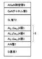
- FIG. 6 is a schematic cross-sectional view showing a laminated structure of a nitride semiconductor epitaxial wafer according to Comparative Example 1.
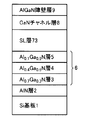
- FIG. 6 is a schematic cross-sectional view showing a laminated structure of a nitride semiconductor epitaxial wafer according to Comparative Example 2.
- FIG. The amount of warpage ( ⁇ m) of the epitaxial wafer depending on the Al composition difference (%) of the superlattice constituent layer having a relatively small band gap in the superlattice buffer layer structure with respect to the uppermost layer in the stepwise compositionally graded buffer layer structure. It is a graph to show.
- FIG. 1 is a schematic cross-sectional view showing a laminated structure of a heterojunction FET epitaxial wafer according to Example 1 of the present invention.
- a Si substrate 1 having a diameter of 4 inches and a thickness of 625 ⁇ m was used.
- the surface oxide film of the Si substrate 1 was removed with a hydrofluoric acid-based etchant, and then the substrate was set in an MOCVD (metal organic vapor deposition) apparatus.
- MOCVD metal organic vapor deposition
- the substrate was heated to 1100 ° C., and the surface of the substrate was cleaned in a hydrogen atmosphere with a chamber internal pressure of 13.3 kPa. Thereafter, nitriding of the Si substrate surface was performed by flowing ammonia NH3 (12.5 slm) while maintaining the substrate temperature and the pressure in the chamber.
- TMG trimethylgallium
- a 1 ⁇ m superlattice (SL) buffer layer structure 7 was formed.
- Example 1 the single GaN channel layer 8 was deposited. However, in order to improve the withstand voltage of the formed FET, the thickness of 0.3 ⁇ m deposited under a relatively low reaction gas pressure is used. A channel layer having a two-layer structure including a GaN layer having a thickness of 0.7 ⁇ m and deposited under a relatively high reaction gas pressure with the GaN layer may be formed. In this case, when the reaction gas pressure is low, carbon contained in TMG is easily doped into the GaN channel layer, and conversely, when the reaction gas pressure is high, the GaN channel layer is not easily doped with carbon. The withstand voltage is improved.
- An electron supply layer consisting of (20 nm thick) was deposited.
- an extremely thin AlN characteristic improving layer (1 nm thickness) is added between the GaN channel layer 8 and the Al0.2Ga0.8N barrier layer 9 to increase the 2DEG concentration in the GaN channel layer.
- an extremely thin AlN characteristic improving layer (1 nm thickness) is added between the GaN channel layer 8 and the Al0.2Ga0.8N barrier layer 9 to increase the 2DEG concentration in the GaN channel layer.
- FIG. 2 is a schematic cross-sectional view showing a laminated structure of an epitaxial wafer for a heterojunction FET according to Comparative Example 1.
- the substrate temperature is set to 1150 ° C., and an AlN superlattice constituting layer having a thickness of 10 nm and a GaN superlattice constituting layer having a thickness of 20 nm are laminated in 70 cycles. It was done.
- Example 2 Thereafter, as in Example 1, an electron supply layer of GaN channel layer 8 (thickness: 1000 nm) and Al0.2Ga0.8N barrier layer 9 (thickness: 20 nm) was deposited.
- FIG. 3 is a schematic cross-sectional view showing a laminated structure of an epitaxial wafer for a heterojunction FET according to Comparative Example 2.
- the layers other than the layer included in the superlattice (SL) buffer layer structure 73 were deposited under the same conditions as in Example 1.
- the substrate temperature was set to 1150 ° C., and an AlN superlattice constituent layer having a thickness of 10 nm and an Al0.2Ga0.8N superlattice constituent layer having a thickness of 20 nm were formed. 70 cycles were laminated.
- Example 2 Thereafter, as in Example 1, an electron supply layer of GaN channel layer 8 (thickness: 1000 nm) and Al0.2Ga0.8N barrier layer 9 (thickness: 20 nm) was deposited.
- Warpage and edge dislocation density were evaluated in the epitaxial wafers according to the examples and comparative examples as described above.
- the warpage of a wafer having a diameter of 4 inches is measured by adding the amount of warpage of the central portion convex downward.
- FWHM and edge dislocation density were related by observation by cathodoluminescence (CL).
- the numerical value “9.0” in the equation (1) is a fitting parameter that relates FWHM and edge dislocation density based on CL observation, and 3.189 ⁇ is the bar gas vector of the edge dislocation in the GaN crystal. Length.
- the composition of the uppermost layer in the stepwise composition gradient buffer layer structure is AlxGa1-xN (0 ⁇ x)
- the composition of the superlattice constituent layer having a relatively large band gap in the superlattice buffer layer structure is AlyGa1-
- yN (y ⁇ 1) and the composition of the superlattice constituent layer having a relatively small band gap is AlzGa1-zN (0 ⁇ z ⁇ y)
- Example 1 the uppermost layer of 6 in the graded composition graded buffer layer structure for the small band gap Al0.1Ga0.9N superlattice constituent layer in the superlattice buffer layer structure 7.
- the Al composition difference of the Al0.1Ga0.9N layer 5 was 0%.
- the amount of warpage of the wafer was 2.0 ⁇ m.
- the edge dislocation density in the wafer was 2.44 ⁇ 109 cm ⁇ 2.
- Comparative Example 1 the Al composition difference of the uppermost Al0.1Ga0.9N layer 5 in the stepwise composition gradient buffer layer structure with respect to the GaN superlattice constituent layer with a small band gap in the superlattice buffer layer structure 71 was ⁇ 10%, and in this case, the amount of warpage of the wafer was 44.8 ⁇ m.
- the edge dislocation density in the wafer was 6.15 ⁇ 10 9 cm ⁇ 2.
- the uppermost Al0.1Ga0.9N layer 5 in the graded composition graded buffer layer structure for the small band gap Al0.2Ga0.8N superlattice constituent layer in the superlattice buffer layer structure 72 The Al composition difference was + 10%, and in this case, the amount of warpage of the wafer was 67.4 ⁇ m. Further, the edge dislocation density in the wafer was 3.45 ⁇ 109 cm ⁇ 2.
- the warp of the epitaxial wafer is 20 ⁇ m or less
- the wafer can be easily handled in the semiconductor manufacturing process, and for example, a GaN-based low on-resistance small power device can be easily manufactured. Therefore, if the composition ratio difference is ⁇ 0.05 ⁇ z ⁇ x ⁇ 0.05, it can be used as a practical epitaxial wafer.
- the Al0.1Ga0.9N layer 5 was used as the uppermost layer in the composition gradient buffer layer structure 6, but the Al0.2Ga0.8N layer was used as the uppermost layer.
- the same tendency as in FIG. 4 was confirmed.
- the AlGaN layer has a lattice constant intermediate between those of the GaN layer and the AlN layer.
- the Al composition of the superlattice constituent layer with the smaller band gap in the superlattice buffer layer structure substantially the same as the Al composition of the uppermost layer in the graded graded buffer layer, It is considered that the distortion between the inclined buffer layer structure and the warp generated in the wafer can be further minimized.
- the superlattice buffer layer structure preferably includes an AlN superlattice constituting layer having as large a band gap as possible.
- the warpage of the nitride-based semiconductor epitaxial wafer can be greatly reduced, and the edge dislocations can be reduced. It is possible to provide a nitride-based semiconductor epitaxial wafer having a reduced density.
Landscapes
- Engineering & Computer Science (AREA)
- Physics & Mathematics (AREA)
- Condensed Matter Physics & Semiconductors (AREA)
- General Physics & Mathematics (AREA)
- Manufacturing & Machinery (AREA)
- Computer Hardware Design (AREA)
- Microelectronics & Electronic Packaging (AREA)
- Power Engineering (AREA)
- Chemical & Material Sciences (AREA)
- Materials Engineering (AREA)
- Junction Field-Effect Transistors (AREA)
Priority Applications (2)
| Application Number | Priority Date | Filing Date | Title |
|---|---|---|---|
| US14/372,366 US9111839B2 (en) | 2012-01-16 | 2013-01-15 | Epitaxial wafer for heterojunction type field effect transistor |
| CN201380005634.XA CN104054166A (zh) | 2012-01-16 | 2013-01-15 | 异质结型场效应晶体管用的外延晶片 |
Applications Claiming Priority (2)
| Application Number | Priority Date | Filing Date | Title |
|---|---|---|---|
| JP2012-005945 | 2012-01-16 | ||
| JP2012005945A JP5785103B2 (ja) | 2012-01-16 | 2012-01-16 | ヘテロ接合型電界効果トランジスタ用のエピタキシャルウエハ |
Publications (1)
| Publication Number | Publication Date |
|---|---|
| WO2013108733A1 true WO2013108733A1 (ja) | 2013-07-25 |
Family
ID=48799158
Family Applications (1)
| Application Number | Title | Priority Date | Filing Date |
|---|---|---|---|
| PCT/JP2013/050519 Ceased WO2013108733A1 (ja) | 2012-01-16 | 2013-01-15 | ヘテロ接合型電界効果トランジスタ用のエピタキシャルウエハ |
Country Status (4)
| Country | Link |
|---|---|
| US (1) | US9111839B2 (enExample) |
| JP (1) | JP5785103B2 (enExample) |
| CN (1) | CN104054166A (enExample) |
| WO (1) | WO2013108733A1 (enExample) |
Cited By (3)
| Publication number | Priority date | Publication date | Assignee | Title |
|---|---|---|---|---|
| CN104201196A (zh) * | 2014-08-13 | 2014-12-10 | 中国电子科技集团公司第五十五研究所 | 表面无微裂纹的Si基III族氮化物外延片 |
| GB2519338A (en) * | 2013-10-17 | 2015-04-22 | Nanogan Ltd | Crack-free gallium nitride materials |
| WO2016166949A1 (ja) * | 2015-04-16 | 2016-10-20 | 株式会社デンソー | 半導体ウエハ及び半導体装置 |
Families Citing this family (25)
| Publication number | Priority date | Publication date | Assignee | Title |
|---|---|---|---|---|
| JP2014220407A (ja) * | 2013-05-09 | 2014-11-20 | ローム株式会社 | 窒化物半導体素子 |
| JP6121806B2 (ja) * | 2013-06-07 | 2017-04-26 | 株式会社東芝 | 窒化物半導体ウェーハ、窒化物半導体素子及び窒化物半導体ウェーハの製造方法 |
| TWI574407B (zh) * | 2013-08-16 | 2017-03-11 | 晶元光電股份有限公司 | 半導體功率元件 |
| CN103500763B (zh) * | 2013-10-15 | 2017-03-15 | 苏州晶湛半导体有限公司 | Ⅲ族氮化物半导体器件及其制造方法 |
| JP2015103665A (ja) * | 2013-11-25 | 2015-06-04 | シャープ株式会社 | 窒化物半導体エピタキシャルウエハおよび窒化物半導体 |
| KR102175320B1 (ko) * | 2014-04-07 | 2020-11-06 | 엘지이노텍 주식회사 | 발광소자 및 이를 구비하는 조명 시스템 |
| CN104037287B (zh) * | 2014-06-10 | 2017-01-11 | 广州市众拓光电科技有限公司 | 生长在Si衬底上的LED外延片及其制备方法 |
| JP2016100471A (ja) * | 2014-11-21 | 2016-05-30 | 住友電気工業株式会社 | 半導体装置及び半導体装置の製造方法 |
| US10109736B2 (en) * | 2015-02-12 | 2018-10-23 | Taiwan Semiconductor Manufacturing Co., Ltd. | Superlattice buffer structure for gallium nitride transistors |
| US20160359004A1 (en) * | 2015-06-03 | 2016-12-08 | Veeco Instruments, Inc. | Stress control for heteroepitaxy |
| US9577042B1 (en) * | 2015-08-13 | 2017-02-21 | Globalfoundries Inc. | Semiconductor structure with multilayer III-V heterostructures |
| CN113506777B (zh) * | 2015-11-02 | 2024-12-13 | 日本碍子株式会社 | 半导体元件用外延基板和半导体元件 |
| US10586701B2 (en) * | 2016-02-26 | 2020-03-10 | Sanken Electric Co., Ltd. | Semiconductor base having a composition graded buffer layer stack |
| US9842900B2 (en) | 2016-03-30 | 2017-12-12 | International Business Machines Corporation | Graded buffer layers with lattice matched epitaxial oxide interlayers |
| CN106098749A (zh) * | 2016-06-30 | 2016-11-09 | 中国电子科技集团公司第五十五研究所 | 一种硅衬底上AlGaN/GaN异质结构及其生长方法 |
| JP6859084B2 (ja) * | 2016-11-30 | 2021-04-14 | 住友化学株式会社 | 半導体基板 |
| JP6796467B2 (ja) * | 2016-11-30 | 2020-12-09 | 住友化学株式会社 | 半導体基板 |
| CN108346694B (zh) | 2017-01-23 | 2020-10-02 | Imec 非营利协会 | 用于电力电子器件的基于iii-n的基材及其制造方法 |
| JP6781095B2 (ja) | 2017-03-31 | 2020-11-04 | エア・ウォーター株式会社 | 化合物半導体基板 |
| CN112820773B (zh) * | 2019-11-18 | 2024-05-07 | 联华电子股份有限公司 | 一种高电子迁移率晶体管 |
| CN111009599B (zh) * | 2020-01-02 | 2025-04-29 | 江西乾照光电有限公司 | 一种led外延片及其制备方法 |
| CN112768512A (zh) * | 2021-01-13 | 2021-05-07 | 西安电子科技大学 | 基于凹槽阳极结构的AlGaN基双沟道肖特基二极管及制备方法 |
| CN114823889A (zh) * | 2021-01-27 | 2022-07-29 | 中国科学院微电子研究所 | 一种半导体功率器件及其制备方法 |
| CN113380930B (zh) * | 2021-06-11 | 2022-08-19 | 厦门士兰明镓化合物半导体有限公司 | 深紫外发光二极管及其制造方法 |
| CN114361302B (zh) * | 2022-03-17 | 2022-06-17 | 江西兆驰半导体有限公司 | 一种发光二极管外延片、发光二极管缓冲层及其制备方法 |
Citations (4)
| Publication number | Priority date | Publication date | Assignee | Title |
|---|---|---|---|---|
| JP2005512327A (ja) * | 2001-12-03 | 2005-04-28 | クリー インコーポレイテッド | へテロ接合トランジスタ及びその製造方法 |
| JP2006100501A (ja) * | 2004-09-29 | 2006-04-13 | Sanken Electric Co Ltd | 半導体素子の形成に使用するための板状基体及びその製造方法 |
| WO2007077666A1 (ja) * | 2005-12-28 | 2007-07-12 | Nec Corporation | 電界効果トランジスタ、ならびに、該電界効果トランジスタの作製に供される多層エピタキシャル膜 |
| JP2009158804A (ja) * | 2007-12-27 | 2009-07-16 | Dowa Electronics Materials Co Ltd | 半導体材料、半導体材料の製造方法及び半導体素子 |
Family Cites Families (9)
| Publication number | Priority date | Publication date | Assignee | Title |
|---|---|---|---|---|
| US7112830B2 (en) * | 2002-11-25 | 2006-09-26 | Apa Enterprises, Inc. | Super lattice modification of overlying transistor |
| JP2007067077A (ja) | 2005-08-30 | 2007-03-15 | Nippon Telegr & Teleph Corp <Ntt> | 窒化物半導体素子およびその製造方法 |
| US7598108B2 (en) * | 2007-07-06 | 2009-10-06 | Sharp Laboratories Of America, Inc. | Gallium nitride-on-silicon interface using multiple aluminum compound buffer layers |
| CN101971308B (zh) * | 2008-03-12 | 2012-12-12 | 日本电气株式会社 | 半导体器件 |
| JP4677499B2 (ja) * | 2008-12-15 | 2011-04-27 | Dowaエレクトロニクス株式会社 | 電子デバイス用エピタキシャル基板およびその製造方法 |
| JP5634681B2 (ja) | 2009-03-26 | 2014-12-03 | 住友電工デバイス・イノベーション株式会社 | 半導体素子 |
| JP5473445B2 (ja) * | 2009-07-17 | 2014-04-16 | シャープ株式会社 | エピタキシャルウェハ |
| JP5708187B2 (ja) * | 2011-04-15 | 2015-04-30 | サンケン電気株式会社 | 半導体装置 |
| JP2013026321A (ja) * | 2011-07-19 | 2013-02-04 | Sharp Corp | 窒化物系半導体層を含むエピタキシャルウエハ |
-
2012
- 2012-01-16 JP JP2012005945A patent/JP5785103B2/ja active Active
-
2013
- 2013-01-15 US US14/372,366 patent/US9111839B2/en active Active
- 2013-01-15 CN CN201380005634.XA patent/CN104054166A/zh active Pending
- 2013-01-15 WO PCT/JP2013/050519 patent/WO2013108733A1/ja not_active Ceased
Patent Citations (4)
| Publication number | Priority date | Publication date | Assignee | Title |
|---|---|---|---|---|
| JP2005512327A (ja) * | 2001-12-03 | 2005-04-28 | クリー インコーポレイテッド | へテロ接合トランジスタ及びその製造方法 |
| JP2006100501A (ja) * | 2004-09-29 | 2006-04-13 | Sanken Electric Co Ltd | 半導体素子の形成に使用するための板状基体及びその製造方法 |
| WO2007077666A1 (ja) * | 2005-12-28 | 2007-07-12 | Nec Corporation | 電界効果トランジスタ、ならびに、該電界効果トランジスタの作製に供される多層エピタキシャル膜 |
| JP2009158804A (ja) * | 2007-12-27 | 2009-07-16 | Dowa Electronics Materials Co Ltd | 半導体材料、半導体材料の製造方法及び半導体素子 |
Cited By (3)
| Publication number | Priority date | Publication date | Assignee | Title |
|---|---|---|---|---|
| GB2519338A (en) * | 2013-10-17 | 2015-04-22 | Nanogan Ltd | Crack-free gallium nitride materials |
| CN104201196A (zh) * | 2014-08-13 | 2014-12-10 | 中国电子科技集团公司第五十五研究所 | 表面无微裂纹的Si基III族氮化物外延片 |
| WO2016166949A1 (ja) * | 2015-04-16 | 2016-10-20 | 株式会社デンソー | 半導体ウエハ及び半導体装置 |
Also Published As
| Publication number | Publication date |
|---|---|
| JP5785103B2 (ja) | 2015-09-24 |
| US20140353587A1 (en) | 2014-12-04 |
| US9111839B2 (en) | 2015-08-18 |
| JP2013145821A (ja) | 2013-07-25 |
| CN104054166A (zh) | 2014-09-17 |
Similar Documents
| Publication | Publication Date | Title |
|---|---|---|
| JP5785103B2 (ja) | ヘテロ接合型電界効果トランジスタ用のエピタキシャルウエハ | |
| JP6318474B2 (ja) | 半導体装置の製造方法 | |
| JP5634681B2 (ja) | 半導体素子 | |
| CN102891174A (zh) | 包括氮化物基半导体层的外延片 | |
| JP5495069B2 (ja) | 半導体素子及びその製造方法 | |
| JP2013145782A (ja) | ヘテロ接合型電界効果トランジスタ用のエピタキシャルウエハ | |
| WO2009119356A1 (ja) | 半導体素子用エピタキシャル基板、半導体素子、および半導体素子用エピタキシャル基板の作製方法 | |
| CN104078500B (zh) | 化合物半导体器件及其制造方法 | |
| CN102870195A (zh) | 外延基板以及外延基板的制造方法 | |
| CN102859653A (zh) | 外延基板以及外延基板的制造方法 | |
| JP2018538686A (ja) | 薄いケイ素基板の応力制御 | |
| CN113921608B (zh) | Iii族氮化物层叠物、半导体元件和iii族氮化物层叠物的制造方法 | |
| JP5817283B2 (ja) | 半導体装置の製造方法 | |
| JP5914999B2 (ja) | 半導体装置の製造方法 | |
| JP2015103665A (ja) | 窒化物半導体エピタキシャルウエハおよび窒化物半導体 | |
| JP6205497B2 (ja) | 窒化物半導体の製造方法 | |
| JP5776344B2 (ja) | 半導体装置 | |
| US9401420B2 (en) | Semiconductor device | |
| JP2014192226A (ja) | 電子デバイス用エピタキシャル基板 | |
| JP2013069935A (ja) | 半導体基板の製造方法 | |
| WO2016152106A1 (ja) | 半導体ウエハ、半導体装置及び半導体ウエハの製造方法 | |
| JP2013069938A (ja) | 半導体基板の製造方法 | |
| JP2013069939A (ja) | 半導体基板および半導体基板の製造方法 | |
| WO2016039178A1 (ja) | 窒化物半導体積層構造及びそれを用いた電子デバイス | |
| CN106057658A (zh) | 气相生长方法 |
Legal Events
| Date | Code | Title | Description |
|---|---|---|---|
| 121 | Ep: the epo has been informed by wipo that ep was designated in this application |
Ref document number: 13739024 Country of ref document: EP Kind code of ref document: A1 |
|
| WWE | Wipo information: entry into national phase |
Ref document number: 14372366 Country of ref document: US |
|
| 122 | Ep: pct application non-entry in european phase |
Ref document number: 13739024 Country of ref document: EP Kind code of ref document: A1 |
|
| NENP | Non-entry into the national phase |
Ref country code: DE |