WO2012169213A1 - 半導体デバイス、半導体基板、半導体基板の製造方法および半導体デバイスの製造方法 - Google Patents
半導体デバイス、半導体基板、半導体基板の製造方法および半導体デバイスの製造方法 Download PDFInfo
- Publication number
- WO2012169213A1 WO2012169213A1 PCT/JP2012/003788 JP2012003788W WO2012169213A1 WO 2012169213 A1 WO2012169213 A1 WO 2012169213A1 JP 2012003788 W JP2012003788 W JP 2012003788W WO 2012169213 A1 WO2012169213 A1 WO 2012169213A1
- Authority
- WO
- WIPO (PCT)
- Prior art keywords
- semiconductor crystal
- crystal layer
- semiconductor
- layer
- substrate
- Prior art date
- Legal status (The legal status is an assumption and is not a legal conclusion. Google has not performed a legal analysis and makes no representation as to the accuracy of the status listed.)
- Ceased
Links
Images






Classifications
-
- H—ELECTRICITY
- H10—SEMICONDUCTOR DEVICES; ELECTRIC SOLID-STATE DEVICES NOT OTHERWISE PROVIDED FOR
- H10D—INORGANIC ELECTRIC SEMICONDUCTOR DEVICES
- H10D84/00—Integrated devices formed in or on semiconductor substrates that comprise only semiconducting layers, e.g. on Si wafers or on GaAs-on-Si wafers
- H10D84/80—Integrated devices formed in or on semiconductor substrates that comprise only semiconducting layers, e.g. on Si wafers or on GaAs-on-Si wafers characterised by the integration of at least one component covered by groups H10D12/00 or H10D30/00, e.g. integration of IGFETs
- H10D84/82—Integrated devices formed in or on semiconductor substrates that comprise only semiconducting layers, e.g. on Si wafers or on GaAs-on-Si wafers characterised by the integration of at least one component covered by groups H10D12/00 or H10D30/00, e.g. integration of IGFETs of only field-effect components
- H10D84/83—Integrated devices formed in or on semiconductor substrates that comprise only semiconducting layers, e.g. on Si wafers or on GaAs-on-Si wafers characterised by the integration of at least one component covered by groups H10D12/00 or H10D30/00, e.g. integration of IGFETs of only field-effect components of only insulated-gate FETs [IGFET]
- H10D84/85—Complementary IGFETs, e.g. CMOS
-
- H—ELECTRICITY
- H10—SEMICONDUCTOR DEVICES; ELECTRIC SOLID-STATE DEVICES NOT OTHERWISE PROVIDED FOR
- H10D—INORGANIC ELECTRIC SEMICONDUCTOR DEVICES
- H10D30/00—Field-effect transistors [FET]
- H10D30/40—FETs having zero-dimensional [0D], one-dimensional [1D] or two-dimensional [2D] charge carrier gas channels
- H10D30/47—FETs having zero-dimensional [0D], one-dimensional [1D] or two-dimensional [2D] charge carrier gas channels having two-dimensional [2D] charge carrier gas channels, e.g. nanoribbon FETs or high electron mobility transistors [HEMT]
-
- H—ELECTRICITY
- H10—SEMICONDUCTOR DEVICES; ELECTRIC SOLID-STATE DEVICES NOT OTHERWISE PROVIDED FOR
- H10D—INORGANIC ELECTRIC SEMICONDUCTOR DEVICES
- H10D84/00—Integrated devices formed in or on semiconductor substrates that comprise only semiconducting layers, e.g. on Si wafers or on GaAs-on-Si wafers
- H10D84/01—Manufacture or treatment
- H10D84/0123—Integrating together multiple components covered by H10D12/00 or H10D30/00, e.g. integrating multiple IGBTs
- H10D84/0126—Integrating together multiple components covered by H10D12/00 or H10D30/00, e.g. integrating multiple IGBTs the components including insulated gates, e.g. IGFETs
- H10D84/0165—Integrating together multiple components covered by H10D12/00 or H10D30/00, e.g. integrating multiple IGBTs the components including insulated gates, e.g. IGFETs the components including complementary IGFETs, e.g. CMOS devices
-
- H—ELECTRICITY
- H10—SEMICONDUCTOR DEVICES; ELECTRIC SOLID-STATE DEVICES NOT OTHERWISE PROVIDED FOR
- H10D—INORGANIC ELECTRIC SEMICONDUCTOR DEVICES
- H10D84/00—Integrated devices formed in or on semiconductor substrates that comprise only semiconducting layers, e.g. on Si wafers or on GaAs-on-Si wafers
- H10D84/01—Manufacture or treatment
- H10D84/0123—Integrating together multiple components covered by H10D12/00 or H10D30/00, e.g. integrating multiple IGBTs
- H10D84/0126—Integrating together multiple components covered by H10D12/00 or H10D30/00, e.g. integrating multiple IGBTs the components including insulated gates, e.g. IGFETs
- H10D84/0165—Integrating together multiple components covered by H10D12/00 or H10D30/00, e.g. integrating multiple IGBTs the components including insulated gates, e.g. IGFETs the components including complementary IGFETs, e.g. CMOS devices
- H10D84/0167—Manufacturing their channels
-
- H—ELECTRICITY
- H10—SEMICONDUCTOR DEVICES; ELECTRIC SOLID-STATE DEVICES NOT OTHERWISE PROVIDED FOR
- H10D—INORGANIC ELECTRIC SEMICONDUCTOR DEVICES
- H10D84/00—Integrated devices formed in or on semiconductor substrates that comprise only semiconducting layers, e.g. on Si wafers or on GaAs-on-Si wafers
- H10D84/01—Manufacture or treatment
- H10D84/02—Manufacture or treatment characterised by using material-based technologies
- H10D84/03—Manufacture or treatment characterised by using material-based technologies using Group IV technology, e.g. silicon technology or silicon-carbide [SiC] technology
- H10D84/038—Manufacture or treatment characterised by using material-based technologies using Group IV technology, e.g. silicon technology or silicon-carbide [SiC] technology using silicon technology, e.g. SiGe
-
- H—ELECTRICITY
- H10—SEMICONDUCTOR DEVICES; ELECTRIC SOLID-STATE DEVICES NOT OTHERWISE PROVIDED FOR
- H10D—INORGANIC ELECTRIC SEMICONDUCTOR DEVICES
- H10D84/00—Integrated devices formed in or on semiconductor substrates that comprise only semiconducting layers, e.g. on Si wafers or on GaAs-on-Si wafers
- H10D84/01—Manufacture or treatment
- H10D84/02—Manufacture or treatment characterised by using material-based technologies
- H10D84/05—Manufacture or treatment characterised by using material-based technologies using Group III-V technology
-
- H—ELECTRICITY
- H10—SEMICONDUCTOR DEVICES; ELECTRIC SOLID-STATE DEVICES NOT OTHERWISE PROVIDED FOR
- H10D—INORGANIC ELECTRIC SEMICONDUCTOR DEVICES
- H10D84/00—Integrated devices formed in or on semiconductor substrates that comprise only semiconducting layers, e.g. on Si wafers or on GaAs-on-Si wafers
- H10D84/01—Manufacture or treatment
- H10D84/02—Manufacture or treatment characterised by using material-based technologies
- H10D84/08—Manufacture or treatment characterised by using material-based technologies using combinations of technologies, e.g. using both Si and SiC technologies or using both Si and Group III-V technologies
-
- H—ELECTRICITY
- H10—SEMICONDUCTOR DEVICES; ELECTRIC SOLID-STATE DEVICES NOT OTHERWISE PROVIDED FOR
- H10D—INORGANIC ELECTRIC SEMICONDUCTOR DEVICES
- H10D84/00—Integrated devices formed in or on semiconductor substrates that comprise only semiconducting layers, e.g. on Si wafers or on GaAs-on-Si wafers
- H10D84/80—Integrated devices formed in or on semiconductor substrates that comprise only semiconducting layers, e.g. on Si wafers or on GaAs-on-Si wafers characterised by the integration of at least one component covered by groups H10D12/00 or H10D30/00, e.g. integration of IGFETs
- H10D84/82—Integrated devices formed in or on semiconductor substrates that comprise only semiconducting layers, e.g. on Si wafers or on GaAs-on-Si wafers characterised by the integration of at least one component covered by groups H10D12/00 or H10D30/00, e.g. integration of IGFETs of only field-effect components
- H10D84/83—Integrated devices formed in or on semiconductor substrates that comprise only semiconducting layers, e.g. on Si wafers or on GaAs-on-Si wafers characterised by the integration of at least one component covered by groups H10D12/00 or H10D30/00, e.g. integration of IGFETs of only field-effect components of only insulated-gate FETs [IGFET]
- H10D84/85—Complementary IGFETs, e.g. CMOS
- H10D84/856—Complementary IGFETs, e.g. CMOS the complementary IGFETs having different architectures than each other, e.g. high-voltage and low-voltage CMOS
-
- H—ELECTRICITY
- H10—SEMICONDUCTOR DEVICES; ELECTRIC SOLID-STATE DEVICES NOT OTHERWISE PROVIDED FOR
- H10D—INORGANIC ELECTRIC SEMICONDUCTOR DEVICES
- H10D86/00—Integrated devices formed in or on insulating or conducting substrates, e.g. formed in silicon-on-insulator [SOI] substrates or on stainless steel or glass substrates
- H10D86/01—Manufacture or treatment
-
- H—ELECTRICITY
- H10—SEMICONDUCTOR DEVICES; ELECTRIC SOLID-STATE DEVICES NOT OTHERWISE PROVIDED FOR
- H10D—INORGANIC ELECTRIC SEMICONDUCTOR DEVICES
- H10D86/00—Integrated devices formed in or on insulating or conducting substrates, e.g. formed in silicon-on-insulator [SOI] substrates or on stainless steel or glass substrates
- H10D86/201—Integrated devices formed in or on insulating or conducting substrates, e.g. formed in silicon-on-insulator [SOI] substrates or on stainless steel or glass substrates the substrates comprising an insulating layer on a semiconductor body, e.g. SOI
-
- H—ELECTRICITY
- H10—SEMICONDUCTOR DEVICES; ELECTRIC SOLID-STATE DEVICES NOT OTHERWISE PROVIDED FOR
- H10D—INORGANIC ELECTRIC SEMICONDUCTOR DEVICES
- H10D87/00—Integrated devices comprising both bulk components and either SOI or SOS components on the same substrate
-
- H—ELECTRICITY
- H10—SEMICONDUCTOR DEVICES; ELECTRIC SOLID-STATE DEVICES NOT OTHERWISE PROVIDED FOR
- H10P—GENERIC PROCESSES OR APPARATUS FOR THE MANUFACTURE OR TREATMENT OF DEVICES COVERED BY CLASS H10
- H10P10/00—Bonding of wafers, substrates or parts of devices
-
- H—ELECTRICITY
- H10—SEMICONDUCTOR DEVICES; ELECTRIC SOLID-STATE DEVICES NOT OTHERWISE PROVIDED FOR
- H10P—GENERIC PROCESSES OR APPARATUS FOR THE MANUFACTURE OR TREATMENT OF DEVICES COVERED BY CLASS H10
- H10P90/00—Preparation of wafers not covered by a single main group of this subclass, e.g. wafer reinforcement
- H10P90/19—Preparing inhomogeneous wafers
- H10P90/1904—Preparing vertically inhomogeneous wafers
-
- H—ELECTRICITY
- H10—SEMICONDUCTOR DEVICES; ELECTRIC SOLID-STATE DEVICES NOT OTHERWISE PROVIDED FOR
- H10P—GENERIC PROCESSES OR APPARATUS FOR THE MANUFACTURE OR TREATMENT OF DEVICES COVERED BY CLASS H10
- H10P90/00—Preparation of wafers not covered by a single main group of this subclass, e.g. wafer reinforcement
- H10P90/19—Preparing inhomogeneous wafers
- H10P90/1904—Preparing vertically inhomogeneous wafers
- H10P90/1906—Preparing SOI wafers
- H10P90/1914—Preparing SOI wafers using bonding
-
- H—ELECTRICITY
- H10—SEMICONDUCTOR DEVICES; ELECTRIC SOLID-STATE DEVICES NOT OTHERWISE PROVIDED FOR
- H10P—GENERIC PROCESSES OR APPARATUS FOR THE MANUFACTURE OR TREATMENT OF DEVICES COVERED BY CLASS H10
- H10P90/00—Preparation of wafers not covered by a single main group of this subclass, e.g. wafer reinforcement
- H10P90/19—Preparing inhomogeneous wafers
- H10P90/1904—Preparing vertically inhomogeneous wafers
- H10P90/1906—Preparing SOI wafers
- H10P90/1922—Preparing SOI wafers using silicon etch back techniques, e.g. BESOI or ELTRAN
-
- H—ELECTRICITY
- H10—SEMICONDUCTOR DEVICES; ELECTRIC SOLID-STATE DEVICES NOT OTHERWISE PROVIDED FOR
- H10W—GENERIC PACKAGES, INTERCONNECTIONS, CONNECTORS OR OTHER CONSTRUCTIONAL DETAILS OF DEVICES COVERED BY CLASS H10
- H10W10/00—Isolation regions in semiconductor bodies between components of integrated devices
- H10W10/10—Isolation regions comprising dielectric materials
- H10W10/181—Semiconductor-on-insulator [SOI] isolation regions, e.g. buried oxide regions of SOI wafers
Definitions
- the present invention relates to a semiconductor device, a semiconductor substrate, a semiconductor substrate manufacturing method, and a semiconductor device manufacturing method.
- this application is a research project commissioned by the New Energy and Industrial Technology Development Organization, “Development of New Nanoelectronic Semiconductor Materials and New Structure Nanoelectronic Device Technology-Research and Development of III-V Group Semiconductor Channel Transistor Technology on Silicon Platform” "It is a patent application subject to Article 19 of the Industrial Technology Strengthening Act.
- Non-Patent Document 1 discloses a CMOSFET structure in which an N-channel MOSFET having a III-V group compound semiconductor channel and a P-channel MOSFET having Ge channel are formed on a single substrate.
- Non-Patent Document 1 S. Takagi, et al., SSE, vol. 51, pp. 526-536, 2007.
- nMISFET Metal-Insulator-Semiconductor-Field-Effect-Transistor
- n-MISFET P-channel MISFET
- CMOS complementary Metal-Insulator-Semiconductor Field-Effect Transistor
- a manufacturing process in which nMISFET and pMISFET are formed at the same time is adopted. Is preferred.
- the process can be simplified, and the device can be easily reduced in size and miniaturized.
- the source / drain formation region of the nMISFET and the source / drain formation region of the pMISFET are formed as a thin film of a material to be the source and drain, and further patterned by photolithography or the like, thereby forming the source / drain of the nMISFET
- the source and drain of the pMISFET can be formed simultaneously.
- the III-V compound semiconductor crystal layer in which the nMISFET is formed and the IV group semiconductor crystal layer in which the pMISFET is formed are different in material.
- the resistance of one or both of the source / drain regions of the nMISFET or pMISFET increases, or the contact resistance between the source / drain regions of one or both of the nMISFET or pMISFET and the source / drain electrodes increases. Therefore, it is difficult to reduce the resistance of the source / drain regions of both nMISFET and pMISFET or the contact resistance with the source / drain electrodes.
- An object of the present invention is to form a CMISFET composed of an nMISFET whose channel is a III-V group compound semiconductor and a pMISFET whose channel is a group IV semiconductor on one substrate. It is an object of the present invention to provide a semiconductor device and a manufacturing method thereof in which each source and each drain are formed simultaneously and the resistance of the source / drain region or the contact resistance with the source / drain electrode is reduced. Moreover, it is providing the semiconductor substrate suitable for such a technique.
- a base substrate, a first semiconductor crystal layer positioned above the base substrate, and a position above a partial region of the first semiconductor crystal layer are provided.
- a second MISFET having a second source and a second drain is provided.
- the first MISFET is a first channel type MISFET
- the second MISFET is different from the first channel type.
- phi 1 of the first semiconductor crystal layer and the second semiconductor crystal layer, the electron affinity of the crystalline part of which constitutes a semiconductor crystal layer of better functioning as an N-type channel
- phi 2 and E g2 are the Of the first semiconductor crystal layer and the second semiconductor crystal layer, the electron affinity and the forbidden band width of the crystal that constitutes the semiconductor crystal layer in which one part functions as a P-type channel are shown.
- a first separation layer located between the base substrate and the first semiconductor crystal layer and electrically separating the base substrate and the first semiconductor crystal layer, and between the first semiconductor crystal layer and the second semiconductor crystal layer And a second separation layer that electrically separates the first semiconductor crystal layer and the second semiconductor crystal layer.
- the semiconductor device may further include a second separation layer located between the first semiconductor crystal layer and the second semiconductor crystal layer and electrically separating the first semiconductor crystal layer and the second semiconductor crystal layer.
- the base substrate and the first semiconductor crystal layer are in contact with each other at the bonding surface, the region of the base substrate in the vicinity of the bonding surface contains impurity atoms exhibiting p-type or n-type conductivity, and the first in the vicinity of the bonding surface.
- the semiconductor crystal layer may contain impurity atoms having a conductivity type different from that of the impurity atoms contained in the base substrate.
- the base substrate may be in contact with the first separation layer.
- the region of the base substrate in contact with the first separation layer is conductive, and the voltage applied to the region of the base substrate in contact with the first separation layer is It may act as a back gate voltage to 1 MISFET.
- the first semiconductor crystal layer and the second separation layer may be in contact with each other.
- the region of the first semiconductor crystal layer that is in contact with the second separation layer is conductive, and the second semiconductor crystal layer and the second separation layer
- the voltage applied to the contact area may act as a back gate voltage to the second MISFET.
- the first MISFET is preferably a P channel type MISFET
- the second MISFET is an N channel type.
- a MISFET is preferable.
- the first MISFET is preferably an N-channel type MISFET
- the second MISFET is a P-channel type.
- a MISFET is preferable.
- Examples of the conductive substance include TiN, TaN, graphene, HfN, and WN.
- a semiconductor substrate for use in the semiconductor device of the first aspect comprising a base substrate, a first semiconductor crystal layer, and a second semiconductor crystal layer, wherein the first semiconductor A semiconductor substrate is provided in which the crystal layer is located above the base substrate and the second semiconductor crystal layer is located above a part or all of the first semiconductor crystal layer.
- a first separation layer located between the base substrate and the first semiconductor crystal layer and electrically separating the base substrate and the first semiconductor crystal layer, and between the first semiconductor crystal layer and the second semiconductor crystal layer And a second separation layer that electrically separates the first semiconductor crystal layer and the second semiconductor crystal layer.
- the first separation layer may be made of an amorphous insulator.
- the first separation layer may be made of a semiconductor crystal having a forbidden band width larger than the forbidden band width of the semiconductor crystal constituting the first semiconductor crystal layer.
- the semiconductor device may further include a second separation layer located between the first semiconductor crystal layer and the second semiconductor crystal layer and electrically separating the first semiconductor crystal layer and the second semiconductor crystal layer.
- the base substrate and the first semiconductor crystal layer are in contact with each other at the bonding surface, the region of the base substrate in the vicinity of the bonding surface contains impurity atoms exhibiting p-type or n-type conductivity, and the first in the vicinity of the bonding surface.
- the semiconductor crystal layer may contain impurity atoms having a conductivity type different from that of the impurity atoms contained in the base substrate.
- the second separation layer examples include those made of an amorphous insulator.
- the second separation layer may be made of a semiconductor crystal having a forbidden band width larger than the forbidden band width of the semiconductor crystal constituting the second semiconductor crystal layer.
- a plurality of second semiconductor crystal layers may be provided. In this case, it is preferable that each of the plurality of second semiconductor crystal layers is regularly arranged in a plane parallel to the upper surface of the base substrate.
- a method of manufacturing a semiconductor substrate according to the second aspect wherein a first semiconductor crystal layer forming step of forming a first semiconductor crystal layer above a base substrate, and a first semiconductor A second semiconductor crystal layer forming step of forming a second semiconductor crystal layer above a partial region of the crystal layer, and the second semiconductor crystal layer forming step includes forming a second semiconductor crystal layer on the semiconductor crystal layer forming substrate.
- a step of forming a second separation layer that electrically separates the first semiconductor crystal layer and the second semiconductor crystal layer, and the second separation layer on the first semiconductor crystal layer and the second semiconductor crystal layer are joined together.
- the second separation layer on the conductor crystal layer and the first semiconductor crystal layer are joined together, or the second separation layer on the first semiconductor crystal layer and the second separation layer on the second semiconductor crystal layer are joined.
- the first semiconductor crystal layer forming step includes an epitaxial growth step of forming the first semiconductor crystal layer on the semiconductor crystal layer formation substrate by an epitaxial crystal growth method, and the base substrate, the first semiconductor crystal layer, or the base substrate. Forming a first separation layer for electrically separating the base substrate and the first semiconductor crystal layer on both the first semiconductor crystal layer and the first semiconductor crystal layer; and the first separation layer and the first semiconductor crystal on the base substrate.
- the first separation layer on the first semiconductor crystal layer and the base substrate are joined so that the layers are joined, or the first separation layer on the base substrate and the first separation on the first semiconductor crystal layer are joined
- a bonding step of bonding the base substrate and the semiconductor crystal layer forming substrate may be provided so that the layers are bonded to each other.
- the first separation layer made of an insulator is formed on the base substrate before the first semiconductor crystal layer formation step.
- the first semiconductor crystal layer forming step may include forming a SiGe layer as a starting material for the first semiconductor crystal layer on the first separation layer; and Heating in an oxidizing atmosphere and oxidizing the surface to increase the concentration of Ge atoms in the SiGe layer.
- the first semiconductor crystal layer is made of a group IV semiconductor crystal and the second semiconductor crystal layer is made of a group III-V compound semiconductor crystal
- the first layer made of an insulator is formed on the surface of the semiconductor layer material substrate made of the group IV semiconductor crystal. Forming a separation layer; implanting cations through the first separation layer to a predetermined depth of separation of the semiconductor layer material substrate; and joining the surface of the first separation layer and the surface of the base substrate.
- the step of modifying the group IV semiconductor crystal located at the expected separation depth, and the position of the group IV semiconductor crystal modified in the step of modifying are located closer to the base substrate. Separating the group IV semiconductor crystal from the semiconductor layer material substrate by separating the semiconductor layer material substrate and the base substrate; and polishing the crystal layer made of the group IV semiconductor crystal remaining on the base substrate. May be.
- the first semiconductor crystal layer forming step Before the first semiconductor crystal layer forming step, a first separation layer made of a semiconductor crystal having a forbidden band width larger than the forbidden band width of the semiconductor crystal constituting the first semiconductor crystal layer is formed on the base substrate by an epitaxial growth method.
- the first semiconductor crystal layer forming step includes a step of forming the first semiconductor crystal layer on the first separation layer by an epitaxial growth method.
- the first semiconductor crystal layer forming step there is a step of forming the first semiconductor crystal layer on the base substrate by an epitaxial growth method.
- impurity atoms having p-type or n-type conductivity may be contained in the vicinity of the surface of the base substrate, and the impurities contained in the base substrate in the step of forming the first semiconductor crystal layer by the epitaxial growth method.
- the first semiconductor crystal layer may be doped with impurity atoms having a conductivity type different from the conductivity type indicated by the atoms.
- a method for manufacturing a semiconductor substrate according to the second aspect wherein a second semiconductor crystal layer is formed on a semiconductor crystal layer forming substrate by an epitaxial crystal growth method.
- the first separation layer on the first semiconductor crystal layer and the base substrate are joined such that the upper first separation layer and the first semiconductor crystal layer are joined, or the first separation layer on the base substrate is joined.
- the crystalline sacrificial layer is epitaxially crystallized on the surface of the semiconductor crystal layer forming substrate before forming the semiconductor crystal layer on the semiconductor crystal layer forming substrate.
- a step of manufacturing a semiconductor substrate having a first semiconductor crystal layer and a second semiconductor crystal layer On each of the first semiconductor crystal layer and the second semiconductor crystal layer, a step of forming a conductive material having a work function ⁇ M satisfying at least one of the relations of Formula 1 and Formula 2 and a gate electrode are formed.
- ⁇ 1 is the electron affinity of the crystal that constitutes the semiconductor crystal layer partly functioning as an N-type channel of the first semiconductor crystal layer and the second semiconductor crystal layer
- ⁇ 2 and E g2 are the first semiconductor crystal layer Of the crystal layer and the second semiconductor crystal layer, the electron affinity and the forbidden band width of a crystal that constitutes a semiconductor crystal layer in which a part functions as a P-type channel are shown.
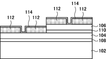
- FIG. 1 shows a cross section of a semiconductor device 100.
- 2 shows a cross section of the semiconductor device 100 in the manufacturing process.
- 2 shows a cross section of the semiconductor device 100 in the manufacturing process.
- 2 shows a cross section of the semiconductor device 100 in the manufacturing process.
- 2 shows a cross section of the semiconductor device 100 in the manufacturing process.
- 2 shows a cross section of the semiconductor device 100 in the manufacturing process.
- 2 shows a cross section of the semiconductor device 100 in the manufacturing process.
- 2 shows a cross section of the semiconductor device 100 in the manufacturing process.
- the cross section in the manufacture process of another semiconductor device is shown.
- the cross section in the manufacture process of another semiconductor device is shown.
- the cross section in the manufacture process of another semiconductor device is shown.
- the cross section in the manufacture process of another semiconductor device is shown.
- the cross section in the manufacture process of another semiconductor device is shown.
- a cross section in the manufacture process of another semiconductor device is shown.
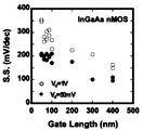
- a cross section of a semiconductor device 200 is shown. It is the SEM photograph which observed nMOSFET from the upper part. It is the TEM photograph which observed the cross section of the gate part of nMOSFET. It is a graph which shows a gate voltage versus source current characteristic. It is a graph which shows a gate voltage versus source current characteristic. It is a graph which shows a gate voltage versus source current characteristic. It is the graph which showed SS value with respect to gate length. It is the graph which showed the value of DIBL with respect to gate length.
- FIG. 1 shows a cross section of the semiconductor device 100.
- the semiconductor device 100 includes a base substrate 102, a first semiconductor crystal layer 104, and a second semiconductor crystal layer 106.
- the semiconductor device 100 of this example includes a first separation layer 108 between the base substrate 102 and the first semiconductor crystal layer 104, and a second separation between the first semiconductor crystal layer 104 and the second semiconductor crystal layer 106.
- a separation layer 110 is included. Note that, from the embodiment shown in FIG. 1, the invention of a semiconductor substrate comprising the base substrate 102, the first semiconductor crystal layer 104, and the second semiconductor crystal layer 106, the base substrate 102, and the first separation.
- At least two inventions can be grasped, including the semiconductor substrate invention having the layer 108, the first semiconductor crystal layer 104, the second separation layer 110, and the second semiconductor crystal layer 106 as constituent elements.
- a first MISFET 120 is formed on the first semiconductor crystal layer 104
- a second MISFET 130 is formed on the second semiconductor crystal layer 106.
- Examples of the base substrate 102 include a substrate whose surface is a silicon crystal.
- Examples of the substrate whose surface is a silicon crystal include a silicon substrate and an SOI (Silicon-on-Insulator) substrate, and a silicon substrate is preferable.
- SOI Silicon-on-Insulator
- the base substrate 102 is not limited to a substrate whose surface is a silicon crystal, and may be an insulator substrate such as glass, ceramics, and plastic, a conductor substrate such as metal, or a semiconductor substrate such as silicon carbide.
- the first semiconductor crystal layer 104 is located above the base substrate 102.
- the first semiconductor crystal layer 104 is made of a group IV semiconductor crystal or a group III-V compound semiconductor crystal.
- the thickness of the first semiconductor crystal layer 104 is preferably 20 nm or less. By setting the thickness of the first semiconductor crystal layer 104 to 20 nm or less, the first MISFET 120 having an extremely thin film body can be configured. By making the body of the first MISFET 120 an extremely thin film, the short channel effect can be suppressed and the leakage current of the first MISFET 120 can be reduced.
- the second semiconductor crystal layer 106 is located above a part of the surface of the first semiconductor crystal layer 104. That is, the second semiconductor crystal layer 106 is located above a part of the region of the first semiconductor crystal layer 104, and the region of the first semiconductor crystal layer 104 where the second semiconductor crystal layer 106 is not located above. A part of these functions as a channel of the first MISFET 120.
- the second semiconductor crystal layer 106 is made of a group III-V compound semiconductor crystal or a group IV semiconductor crystal.
- the thickness of the second semiconductor crystal layer 106 is preferably 20 nm or less. By setting the thickness of the second semiconductor crystal layer 106 to 20 nm or less, the second MISFET 130 having an extremely thin film body can be configured. By making the body of the second MISFET 130 an extremely thin film, the short channel effect can be suppressed and the leakage current of the second MISFET 130 can be reduced.
- the group III-V compound semiconductor crystal has a high electron mobility and the group IV semiconductor crystal, particularly Ge, has a high hole mobility, it is preferable to form an N channel MISFET in the group III-V compound semiconductor crystal layer. It is preferable to form a P-channel MISFET in the group IV semiconductor crystal layer. That is, when the first semiconductor crystal layer 104 is made of a group IV semiconductor crystal and the second semiconductor crystal layer 106 is made of a group III-V compound semiconductor crystal, the first MISFET 120 is a P-channel type MISFET and the second MISFET 130 is an N-channel type. A MISFET is preferable.
- the first MISFET 120 is an N-channel MISFET and the second MISFET 130 is a P-channel.
- a type MISFET is preferable.
- Examples of the group IV semiconductor crystal include a Ge crystal or a Si x Ge 1-x (0 ⁇ x ⁇ 1) crystal. When the group IV semiconductor crystal is a Si x Ge 1-x crystal, x is preferably 0.10 or less.
- Examples of the III-V compound semiconductor crystal include In x Ga 1-x As (0 ⁇ x ⁇ 1) crystal, InAs crystal, GaAs crystal, and InP crystal. Examples of the III-V compound semiconductor crystal include a mixed crystal of a III-V compound semiconductor that lattice matches or pseudo-lattice matches with GaAs or InP.
- the group III-V compound semiconductor crystal the mixed crystal In x Ga 1-x As ( 0 ⁇ x ⁇ 1) crystal, InAs crystal, a laminate of a GaAs crystal or InP crystals, and the like.
- the III-V compound semiconductor crystal In x Ga 1-x As (0 ⁇ x ⁇ 1) crystal and InAs crystal are preferable, and InAs crystal is more preferable.
- the first separation layer 108 is located between the base substrate 102 and the first semiconductor crystal layer 104.
- the first separation layer 108 electrically separates the base substrate 102 and the first semiconductor crystal layer 104.
- the first separation layer 108 may be made of an amorphous insulator.
- the first separation layer 108 is made of an amorphous insulator.
- the first separation layer 108 may be made of a semiconductor crystal having a forbidden band width larger than the forbidden band width of the semiconductor crystal constituting the first semiconductor crystal layer 104.
- a semiconductor crystal can be formed by an epitaxial crystal growth method.
- the semiconductor crystal constituting the first separation layer 108 include an AlGaAs crystal, an AlInGaP crystal, an AlGaInAs crystal, and an InP crystal.
- the semiconductor crystal constituting the first separation layer 108 includes a SiGe crystal, a Si crystal, a SiC crystal, or a C crystal.
- the second separation layer 110 is located between the first semiconductor crystal layer 104 and the second semiconductor crystal layer 106.
- the second separation layer 110 electrically separates the first semiconductor crystal layer 104 and the second semiconductor crystal layer 106.
- the second separation layer 110 may be made of an amorphous insulator.
- the second separation layer 110 becomes an amorphous insulator.
- the second separation layer 110 made of an amorphous insulator Al 2 O 3 , AlN, Ta 2 O 5 , ZrO 2 , HfO 2 , La 2 O 3 , SiO x (for example, SiO 2 ), SiN x (for example, Si) 3 N 4 ) and SiO x N y , or a laminate of at least two layers selected from these layers.
- the second isolation layer 110 may be made of a semiconductor crystal having a forbidden band width larger than the forbidden band width of the semiconductor crystal constituting the second semiconductor crystal layer 106.
- a semiconductor crystal can be formed by an epitaxial crystal growth method.
- the semiconductor crystal layer 106 is an InGaAs crystal layer or a GaAs crystal layer
- examples of the semiconductor crystal include an AlGaAs crystal, an AlInGaP crystal, an AlGaInAs crystal, and an InP crystal.
- the second semiconductor crystal layer 106 is a Ge crystal layer
- examples of the semiconductor crystal include SiGe crystal, Si crystal, SiC crystal, and C crystal.
- the first MISFET 120 is formed in the first semiconductor crystal layer 104 in a region where the second semiconductor crystal layer 106 is not located above, and has a first gate 122, a first source 124, and a first drain 126.
- a first gate metal 123 is formed on the first gate 122, and a first source electrode 125 and a first drain electrode 127 are formed on the first source 124 and the first drain 126, respectively.
- Examples of the material constituting the first gate metal 123, the first source electrode 125, and the first drain electrode 127 include Ti, Ta, W, Al, Cu, Au, and a stacked body thereof.
- the first source 124 and the first drain 126 are made of a conductive material formed on the first semiconductor crystal layer 104, and form a raised source / drain.
- the conductive material include TiN, TaN, graphene, HfN, and WN.
- a first gate 122 is formed between the first source 124 and the first drain 126.
- the first gate 122 is insulated from the first source 124, the first drain 126, and the first semiconductor crystal layer 104 by the insulating layer 114.
- Examples of the material constituting the first gate 122 include TiN, TaN, graphene, HfN, and WN.
- the insulating layer 114 Al 2 O 3 , AlN, Ta 2 O 5 , ZrO 2 , HfO 2 , La 2 O 3 , SiO x (for example, SiO 2 ), SiN x (for example, Si 3 N 4 ), and SiO x N y Among them, a layer composed of at least one of them, or a laminate of at least two layers selected from these.
- a part 114 a of the insulating layer 114 is formed in a region sandwiched between the part 104 a of the first semiconductor crystal layer 104 and the first gate 122, which is the channel region.
- the portion 114a may function as a gate insulating layer.
- the second MISFET 130 is formed in the second semiconductor crystal layer 106 and has a second gate 132, a second source 134, and a second drain 136.
- a second gate metal 133 is formed on the second gate 132, and a second source electrode 135 and a second drain electrode 137 are formed on the second source 134 and the second drain 136, respectively.
- Examples of the material constituting the second gate metal 133, the second source electrode 135, and the second drain electrode 137 include Ti, Ta, W, Al, Cu, Au, and a laminate thereof.
- the second source 134 and the second drain 136 are made of a conductive material formed on the second semiconductor crystal layer 106, and constitute a raised source / drain.
- the conductive material include TiN, TaN, graphene, HfN, and WN.
- a second gate 132 is formed between the second source 134 and the second drain 136.
- the second gate 132 is insulated from the second source 134, the second drain 136, and the second semiconductor crystal layer 106 by the insulating layer 114 similar to the first MISFET 120.
- Examples of the material constituting the second gate 132 include TiN, TaN, graphene, HfN, and WN.
- a part 114 a of the insulating layer 114 is formed in a region sandwiched between the part 106 a of the second semiconductor crystal layer 106 and the second gate 132 which is the channel region.
- the portion 114a may function as a gate insulating layer.
- the first source 124, the first drain 126, the second source 134, and the second drain 136 are made of the same conductive material, and the work function ⁇ M of the conductive material satisfies the relationship of Equation 1 or Equation 2.
- phi 1 shows the electron affinity of the crystalline part of which constitutes a semiconductor crystal layer of better functioning as an N-type channel.
- ⁇ 2 and E g2 indicate the electron affinity and the forbidden band width of the crystal that constitutes the semiconductor crystal layer of which part of the first semiconductor crystal layer 104 and the second semiconductor crystal layer 106 functions as a P-type channel.
- the work function ⁇ M of the conductive material may satisfy both of the relations of Formula 1 and Formula 2.
- the source / drain (first source 124 and first drain 126) of the first MISFET 120 and the source / drain (second source 134 and second drain 136) of the second MISFET 130 are made of the same conductive material. This is a configuration that enables the manufacture of the part using the same material film, and means that the manufacturing process can be simplified.
- the gate width can be easily controlled by the space between the source and the drain (etching groove interval). As a result, miniaturization becomes easy.
- the source / drain The contact resistance between the region and the semiconductor crystal layer can be reduced.
- the work function ⁇ M of the conductive material satisfies the relationship of Equation 1
- the difference between ⁇ M and ⁇ 1 and the difference between ⁇ M and ⁇ 2 + E g2 are ⁇ 1 and ⁇ 2 at the maximum. It becomes smaller than the difference from + Eg2 .
- the contact resistance between each source / drain region and the semiconductor crystal layer can be reduced.
- the work function ⁇ M of the conductive material satisfies the relationship of Equation 2 , the difference between ⁇ M and ⁇ 1 and the difference between ⁇ M and ⁇ 2 + E g2 can be suppressed to 0.1 eV or less. . For this reason, the contact resistance between each source / drain region and the semiconductor crystal layer can be reduced. As a result, the manufacturing process for manufacturing the CMISFET can be simplified, the miniaturization can be facilitated, and the performance of each FET can be enhanced.
- FIG. 2 to 8 show cross sections in the manufacturing process of the semiconductor device 100.
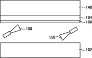
- the base substrate 102 and the semiconductor crystal layer formation substrate 140 are prepared, and the first semiconductor crystal layer 104 is formed on the semiconductor crystal layer formation substrate 140 by an epitaxial crystal growth method. Thereafter, a first separation layer 108 is formed on the first semiconductor crystal layer 104.
- the first separation layer 108 is formed by a thin film formation method such as an ALD (Atomic Layer Deposition) method, a thermal oxidation method, a vapor deposition method, a CVD (Chemical Layer Vapor Deposition) method, or a sputtering method.
- the semiconductor crystal layer formation substrate 140 When the first semiconductor crystal layer 104 is made of a III-V group compound semiconductor crystal, an InP substrate or a GaAs substrate can be selected as the semiconductor crystal layer formation substrate 140. When the first semiconductor crystal layer 104 is made of a group IV semiconductor crystal, a Ge substrate, Si substrate, SiC substrate, or GaAs substrate can be selected as the semiconductor crystal layer formation substrate 140.
- An MOCVD (Metal Organic Chemical Vapor Deposition) method can be used for epitaxial crystal growth of the first semiconductor crystal layer 104.
- TMIn trimethylindium
- TMGa trimethylgallium
- AsH 3 arsine
- P source is used.
- PH 3 phosphine
- Hydrogen can be used as the carrier gas.
- the reaction temperature can be appropriately selected in the range of 300 ° C. to 900 ° C., preferably in the range of 450 to 750 ° C.
- GeH 4 germane
- SiH 4 silane
- Si 2 H 6 diisilane
- a compound in which some of these hydrogen atoms are substituted with chlorine atoms or hydrocarbon groups can also be used.
- Hydrogen can be used as the carrier gas.
- the reaction temperature can be appropriately selected in the range of 300 ° C. to 900 ° C., preferably in the range of 450 to 750 ° C.
- the thickness of the epitaxial growth layer can be controlled by appropriately selecting the source gas supply amount and the reaction time.
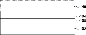
- the surface of the first separation layer 108 and the surface of the base substrate 102 are activated with an argon beam 150. Thereafter, as shown in FIG. 3, the surface of the first separation layer 108 activated by the argon beam 150 and the surface of the base substrate 102 are bonded and bonded together. Bonding can be performed at room temperature. The activation does not need to be performed by the argon beam 150, but may be a beam of other rare gas or the like. Thereafter, the semiconductor crystal layer forming substrate 140 is etched and removed. As a result, the first separation layer 108 and the first semiconductor crystal layer 104 are formed on the base substrate 102. Note that a sulfur termination treatment for terminating the surface of the first semiconductor crystal layer 104 with sulfur atoms may be performed between the formation of the first semiconductor crystal layer 104 and the formation of the first separation layer 108.
- the first separation layer 108 is formed only on the first semiconductor crystal layer 104 and the surface of the first separation layer 108 and the surface of the base substrate 102 are bonded to each other.
- the first separation layer 108 is also formed on the base substrate 102, and the surface of the first separation layer 108 on the first semiconductor crystal layer 104 and the surface of the first separation layer 108 on the base substrate 102 are bonded together. May be.
- the surface of the first separation layer 108 to be bonded is subjected to a hydrophilic treatment. When the hydrophilic treatment is performed, it is preferable that the first separation layers 108 are heated and bonded together.
- the first separation layer 108 may be formed only on the base substrate 102, and the surface of the first semiconductor crystal layer 104 and the surface of the first separation layer 108 on the base substrate 102 may be bonded to each other.
- the first separation layer 108 and the first semiconductor crystal layer 104 are bonded to the semiconductor crystal layer formation substrate.
- the first separation layer 108 and the first semiconductor crystal layer 104 are separated from the base substrate 102. You may stick together.
- the first separation layer 108 and the first semiconductor crystal layer 104 are separated from the semiconductor crystal layer formation substrate 140 and before being bonded to the base substrate 102, the first separation layer 108 and the first separation layer 108 are formed on an appropriate transfer substrate. It is preferable to hold one semiconductor crystal layer 104.
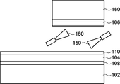
- a semiconductor crystal layer forming substrate 160 is prepared, and the second semiconductor crystal layer 106 is formed on the semiconductor crystal layer forming substrate 160 by an epitaxial crystal growth method.
- a second separation layer 110 is formed on the first semiconductor crystal layer 104 on the base substrate 102.
- the second separation layer 110 is formed by a thin film forming method such as an ALD method, a thermal oxidation method, a vapor deposition method, a CVD method, or a sputtering method.
- a sulfur termination treatment for terminating the surface of the first semiconductor crystal layer 104 with sulfur atoms may be performed before the formation of the second separation layer 110.
- the semiconductor crystal layer 106 is made of a III-V group compound semiconductor crystal
- an InP substrate or a GaAs substrate can be selected as the semiconductor crystal layer forming substrate 160.
- the second semiconductor crystal layer 106 is made of a group IV semiconductor crystal
- a Ge substrate, Si substrate, SiC substrate, or GaAs substrate can be selected as the semiconductor crystal layer forming substrate 160.
- the MOCVD method can be used for epitaxial crystal growth of the second semiconductor crystal layer 106.
- Gas used in the MOCVD method, reaction temperature conditions, and the like are the same as those for the first semiconductor crystal layer 104.
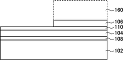
- the surface of the second semiconductor crystal layer 106 and the surface of the second separation layer 110 are activated with an argon beam 150. Thereafter, as shown in FIG. 5, the surface of the second semiconductor crystal layer 106 is bonded to and bonded to a part of the surface of the second separation layer 110. Bonding can be performed at room temperature. The activation does not need to be performed by the argon beam 150 but may be a beam of other rare gas or the like. Thereafter, the semiconductor crystal layer forming substrate 160 is removed by etching with an HCl solution or the like.
- the second separation layer 110 is formed on the first semiconductor crystal layer 104 on the base substrate 102, and the second semiconductor crystal layer 106 is formed on a part of the surface of the second separation layer 110.
- a sulfur termination treatment may be performed in which the surface of the second semiconductor crystal layer 106 is terminated with sulfur atoms.
- the second separation layer 110 is formed only on the first semiconductor crystal layer 104 and the surface of the second separation layer 110 and the surface of the second semiconductor crystal layer 106 are bonded to each other has been described.
- the second separation layer 110 is also formed on the second semiconductor crystal layer 106, and the surface of the second separation layer 110 on the first semiconductor crystal layer 104 and the second separation layer 110 on the second semiconductor crystal layer 106 are formed. You may stick together the surface.
- the second separation layer 110 is formed only on the second semiconductor crystal layer 106, and the surface of the first semiconductor crystal layer 104 and the surface of the second separation layer 110 on the second semiconductor crystal layer 106 are bonded together. Also good.
- the second semiconductor crystal layer 106 is separated from the semiconductor crystal layer formation substrate 160 after the second semiconductor crystal layer 106 is bonded to the second separation layer 110 on the base substrate 102 has been described.
- the second semiconductor crystal layer 106 may be bonded to the second separation layer 110.
- the second semiconductor crystal layer 106 may be held on an appropriate transfer substrate until the second semiconductor crystal layer 106 is bonded to the second separation layer 110. preferable.
- a conductive material layer 112 is formed on the first semiconductor crystal layer 104 and the second semiconductor crystal layer 106.
- the conductive material layer 112 becomes the first source 124, the first drain 126, the second source 134, and the second drain 136 later.
- the conductive material layer 112 is formed by a thin film formation method such as a vapor deposition method, a CVD method, or a sputtering method.
- the conductive material layer 112 in the region of the first MISFET 120 and the second MISFET 130 is separated depending on the thicknesses of the second separation layer 110 and the second semiconductor crystal layer 106.
- the conductive material layer 112 may be separated into regions of the first MISFET 120 and the second MISFET 130 by a method such as etching a part of the conductive material layer 112.
- the conductive material layer 112 in the region where the first gate 122 and the second gate 132 are formed is removed by etching to form an opening.
- an insulating layer 114 is formed inside the conductive material layer 112 and the opening.
- the insulating layer 114 is formed by a thin film forming method such as an ALD method, a thermal oxidation method, a vapor deposition method, a CVD method, or a sputtering method.
- a conductive thin film is formed on the insulating layer 114, and the conductive thin films other than the regions to be the first gate 122 and the second gate 132 are removed, so that the first gate 122 and the second gate A gate 132 is formed.
- the conductive material layer 112 separated by the first gate 122 or the second gate 132 becomes the first source 124, the first drain 126, the second source 134, and the second drain 136.
- An opening is formed in the insulating layer 114 so that the conductive material layer 112 to be the first source 124, the first drain 126, the second source 134, and the second drain 136 is exposed, and the first thin film is formed and patterned to form the first.
- the semiconductor device 100 shown in FIG. 1 can be manufactured.
- a metal film is formed as the conductive thin film, it is preferable to perform post metal annealing treatment.
- the post metal annealing treatment is preferably carried out by an RTA (rapid thermal annealing) method.
- the first source 124, the first drain 126, the second source 134, and the second drain 136 are simultaneously formed in the same process, so that the manufacturing process can be simplified. .
- manufacturing costs are reduced and miniaturization is facilitated.
- the work functions of the conductive materials constituting the first source 124, the first drain 126, the second source 134, and the second drain 136 satisfy the relationship represented by Equation 1 or Equation 2. Therefore, the contact between the first source 124 and the first drain 126 and the first semiconductor crystal layer 104 is an ohmic contact, and the contact between the second source 134 and the second drain 136 and the second semiconductor crystal layer 106 is an ohmic contact.
- each on-current of the first MISFET 120 and the second MISFET 130 can be increased. Further, since the resistance between each source and drain is reduced, it is not necessary to reduce the channel resistance of each MISFET, and the concentration of doping impurity atoms in the channel layer can be reduced. As a result, carrier mobility in the channel layer can be increased.
- the first separation of the base substrate 102 is performed.
- a voltage can be applied to a region in contact with the layer 108 and the voltage can act as a back gate voltage to the first MISFET 120.
- the semiconductor device 100 described above since the first semiconductor crystal layer 104 and the second separation layer 110 are in contact with each other, if the region of the first semiconductor crystal layer 104 in contact with the second separation layer 110 is conductive.
- a voltage can be applied to the region of the first semiconductor crystal layer 104 that is in contact with the second isolation layer 110, and this voltage can act as a back gate voltage to the second MISFET 130.
- the action of these back gate voltages can increase the on-current of the first MISFET 120 and the second MISFET 130 and reduce the off-current.
- the semiconductor device 100 described above may include a plurality of second semiconductor crystal layers 106, and each of the plurality of second semiconductor crystal layers 106 may be regularly arranged in a plane parallel to the upper surface of the base substrate 102. Regular means that the same arrangement pattern is repeated, for example.
- the semiconductor device 100 may include a plurality of first semiconductor crystal layers 104, and each of the plurality of first semiconductor crystal layers 104 may be regularly arranged in a plane parallel to the upper surface of the base substrate 102. Good.
- each first semiconductor crystal layer 104 may have a single semiconductor crystal layer 106 or a plurality of second semiconductor crystal layers 106, and each second semiconductor crystal layer 106 is parallel to the upper surface of the first semiconductor crystal layer 104. May be regularly arranged in a plane.
- the productivity of the semiconductor substrate used for the semiconductor device 100 can be increased.
- the regular arrangement of the second semiconductor crystal layer 106 or the first semiconductor crystal layer 104 is such that the second semiconductor crystal layer 106 or the first semiconductor crystal layer is grown after epitaxially growing the second semiconductor crystal layer 106 or the first semiconductor crystal layer 104.
- the first semiconductor crystal layer 104 and the first isolation layer 108 are formed on the semiconductor crystal layer formation substrate 140, and the first isolation layer 108 and the base substrate 102 are bonded together, and then the semiconductor crystal layer formation is performed. It has been described that the first semiconductor crystal layer 104 and the first separation layer 108 are formed on the base substrate 102 by removing the substrate 140. However, when the first semiconductor crystal layer 104 is made of SiGe and the second semiconductor crystal layer 106 is made of a group III-V compound semiconductor crystal, the first semiconductor crystal layer 104 and the first separation layer 108 are formed by an oxidation concentration method.
- the first separation layer 108 made of an insulator is formed on the base substrate 102, and the first semiconductor crystal layer 104 starts on the first separation layer 108.
- a SiGe layer as a material is formed.
- the SiGe layer is heated in an oxidizing atmosphere to oxidize the surface. By oxidizing the SiGe layer, the concentration of Ge atoms in the SiGe layer can be increased, and the first semiconductor crystal layer 104 having a high Ge concentration can be obtained.
- the first semiconductor crystal layer 104 and the first separation layer 108 are smart cut. It can be formed by the method. That is, a first separation layer 108 made of an insulator is formed on the surface of a semiconductor layer material substrate made of a group IV semiconductor crystal, and cations are implanted through the first separation layer 108 to a predetermined separation depth of the semiconductor layer material substrate. To do. The semiconductor layer material substrate and the base substrate 102 are attached to each other so that the surface of the first separation layer 108 and the surface of the base substrate 102 are bonded, and the semiconductor layer material substrate and the base substrate 102 are heated.
- the cations implanted at the planned separation depth react with the group IV atoms constituting the semiconductor layer material substrate, and the group IV semiconductor crystal located at the planned separation depth is denatured. If the semiconductor layer material substrate and the base substrate 102 are separated in this state, the group IV semiconductor crystal located on the base substrate 102 side from the modified group of the group IV semiconductor crystal is separated from the semiconductor layer material substrate. If the semiconductor layer material attached to the base substrate 102 side is appropriately polished, the polished semiconductor crystal layer can be used as the first semiconductor crystal layer 104.
- the first isolation layer 108 when the first separation layer 108 is a semiconductor crystal having a forbidden band width larger than the forbidden band width of the semiconductor crystal constituting the first semiconductor crystal layer 104,
- the first isolation layer 108 can be formed by an epitaxial growth method, and the first semiconductor crystal layer 104 can be formed on the first isolation layer 108 by an epitaxial growth method. Since the first separation layer 108 and the first semiconductor crystal layer 104 can be continuously formed by the epitaxial growth method, the manufacturing process is simplified.
- the second separation layer 110 is a semiconductor crystal having a forbidden band width larger than that of the semiconductor crystal constituting the second semiconductor crystal layer 106
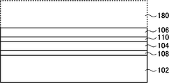
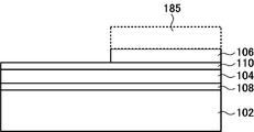
- the second semiconductor crystal layer 106, the second The two separation layers 110 and the first semiconductor crystal layer 104 can be continuously formed by an epitaxial growth method. That is, as shown in FIG. 9, the second semiconductor crystal layer 106 is formed on the semiconductor crystal layer forming substrate 180 by the epitaxial crystal growth method, and the second separation layer 110 is epitaxially formed on the second semiconductor crystal layer 106.
- a first semiconductor crystal layer 104 is formed on the second isolation layer 110 by an epitaxial crystal growth method. These epitaxial growths can be performed continuously.
- a first separation layer 108 is formed on the first semiconductor crystal layer 104, and the surface of the first separation layer 108 and the surface of the base substrate 102 are activated with an argon beam 150.
- the surface of the first separation layer 108 and the surface of the base substrate 102 are bonded together, and the semiconductor crystal layer forming substrate 180 is etched and removed with an HCl solution or the like.
- a part of the second semiconductor crystal layer 106 is etched using a mask 185, whereby a semiconductor substrate similar to that in FIG. 5 can be obtained.
- the second semiconductor crystal layer 106, the second separation layer 110, and the first semiconductor crystal layer 104 can be continuously formed by an epitaxial growth method, so that the manufacturing process is simplified.
- the first step is performed on either or both of the base substrate 102 and the first semiconductor crystal layer 104.
- One separation layer 108 may be formed.
- the first separation layer 108, the first semiconductor crystal layer 104, the second separation layer 110, and the second semiconductor crystal layer 106 may be transferred to an appropriate transfer substrate and then bonded to the base substrate 102.
- the second isolation layer 110 is an epitaxially grown crystal
- the first isolation crystal layer 104, the second isolation layer 110, and the second semiconductor crystal layer 106 are bonded to the base substrate 102, and then the second isolation layer 110 is oxidized. Then, it may be converted into an amorphous insulator layer.
- the second separation layer 110 is AlAs or AlInP
- the second separation layer 110 can be made of an insulating oxide by a selective oxidation technique.
- the substrate can also be removed. That is, before forming the first semiconductor crystal layer 104 on the semiconductor crystal layer formation substrate 140, the crystalline sacrificial layer 190 is formed on the surface of the semiconductor crystal layer formation substrate 140 by an epitaxial crystal growth method. Thereafter, the first semiconductor crystal layer 104 and the first separation layer 108 are formed on the surface of the crystalline sacrificial layer 190 by an epitaxial growth method, and the surface of the first separation layer 108 and the surface of the base substrate 102 are activated by the argon beam 150. .
- the semiconductor crystal layer forming substrate can be reused, and the manufacturing cost can be reduced.
- FIG. 14 shows a cross section of the semiconductor device 200.
- the semiconductor device 200 does not have the first separation layer 108 in the semiconductor device 100, and the first semiconductor crystal layer 104 is disposed in contact with the base substrate 102.
- the first separation layer 108 since it has the same structure as the semiconductor device 100 except that the first separation layer 108 is not provided, description of common members and the like is omitted.
- the base substrate 102 and the first semiconductor crystal layer 104 are in contact with each other at the bonding surface 103, and contain impurity atoms having p-type or n-type conductivity in the vicinity of the bonding surface 103 of the base substrate 102.
- impurity atoms having a conductivity type different from the conductivity type indicated by the impurity atoms contained in the base substrate 102 are contained. That is, the semiconductor device 200 has a pn junction in the vicinity of the bonding surface 103.
- the base substrate 102 and the first semiconductor crystal layer 104 can be electrically separated by a pn junction formed in the vicinity of the bonding surface 103.
- the first MISFET 120 formed in the semiconductor crystal layer 104 can be electrically isolated from the base substrate 102.
- Such separation by the pn junction can also be applied between the first semiconductor crystal layer 104 and the second semiconductor crystal layer 106. That is, in the structure in which the second semiconductor layer 104 is not in contact with the first semiconductor crystal layer 104 and the second semiconductor crystal layer 106 are in contact with each other at the junction surface, the p-type or An impurity atom having an n-type conductivity type is contained, and a conductivity type different from the conductivity type indicated by the impurity atom contained in the first semiconductor crystal layer 104 is present in the vicinity of the junction surface of the second semiconductor crystal layer 106. Contains impurity atoms.
- first semiconductor crystal layer 104 and the second semiconductor crystal layer 106 can be electrically separated, and the first MISFET 120 formed in the first semiconductor crystal layer 104 and the second MISFET 130 formed in the second semiconductor crystal layer 106 are electrically connected. Can be separated.
- the steps after the step of forming the first semiconductor crystal layer 104 on the base substrate 102 by the epitaxial growth method and forming the second isolation layer 110 on the first semiconductor crystal layer 104 are the same as those in the semiconductor device 200. It can be manufactured by performing the same process as in the case of the device 100.
- the base substrate 102 is formed in a step in which impurity atoms having p-type or n-type conductivity are contained in the vicinity of the surface of the base substrate 102 and the first semiconductor crystal layer 104 is formed by the epitaxial growth method.
- the first semiconductor crystal layer 104 can be doped with an impurity atom having a conductivity type different from that of the impurity atom contained in the first semiconductor crystal layer 104.
- the pn junction as the isolation structure is not essential when the need for element isolation is low. That is, the semiconductor device 200 does not contain an impurity atom having p-type or n-type conductivity in the vicinity of the bonding surface 103 of the base substrate 102, and is p-type or in the vicinity of the bonding surface 103 of the first semiconductor crystal layer 104. A structure not containing an impurity atom exhibiting n-type conductivity may be used.
- the epitaxial growth method is a method in which the first semiconductor crystal layer 104 is uniformly grown on the entire surface of the base substrate 102, or the surface of the base substrate 102 is divided finely by a growth inhibition layer such as SiO 2 and selectively. Any epitaxial growth method may be used.
- a semiconductor substrate having a Ge crystal layer above a part of the surface of the base substrate and having an InGaAs crystal layer above the other part of the surface of the base substrate where the Ge crystal layer is not located above is used.
- this embodiment is different from the semiconductor substrate of the present invention having the first semiconductor crystal layer 104 on the base substrate 102 and the second semiconductor crystal layer 106 on the first semiconductor crystal layer 104.
- the configurations of the following embodiments are also related to FIG. Similar results can be obtained with the configuration of the semiconductor device 100 described above.
- each of the first semiconductor crystal layer 104 and the second semiconductor crystal layer 106 in the present invention is a Ge crystal layer and an InGaAs crystal layer
- the same results as in the following examples can be obtained from the above-described viewpoint. Can be estimated. Therefore, the following examples will be described as an example of the effects expected in the present invention.
- a Ge crystal layer was formed on a part of the surface of the base substrate, and an InGaAs crystal layer was formed on the other part of the surface of the base substrate, that is, on the base substrate in a region where the Ge crystal layer was not formed.
- a TaN layer having a thickness of 30 nm was deposited on the InGaAs crystal layer and the Ge crystal layer, and the TaN layer was patterned. By the patterning, a source and a drain were formed on each of the InGaAs crystal layer and the Ge crystal layer.
- An Al 2 O 3 / TaN laminated film was deposited in the order of Al 2 O 3 and TaN so as to fill the trench between the source and drain, and the deposited layer was patterned to form a gate insulating film and a gate.
- FIG. 15 is a SEM photograph of the nMOSFET observed from above.
- a gate electrode is formed so as to overlap a gap (groove between source and drain) indicated by Lg.
- FIG. 16 is a TEM photograph observing a cross section of the gate portion of the nMOSFET. Even when the gate length Lg is 50 nm, it can be confirmed that the trench between the source and the drain is securely buried.
- the source / drain made of TaN formed as described above has a work function of about 4.6 eV.
- the electron affinity of InGaAs is 4.5 eV
- the electron affinity of Ge is 4.0 eV
- the band gap of Ge is 0.67 eV. Therefore, the work function ⁇ M of the source / drain is such that the electron affinity ⁇ 1 of InGaAs which is an nMOSFET material and the sum of electron affinity and band gap ⁇ 2 + E g2 of Ge which is a pMOSFET material are ⁇ 1 ⁇ M ⁇ The relationship of 2 + E g2 is satisfied.
- between the work function ⁇ M of the source / drain and the electron affinity ⁇ 1 of InGaAs is 0.1 eV or less, and the work function ⁇ M of the source / drain and the electron affinity of Ge and The sum of the band gap ⁇ 2 + E g2 and the difference
- are also 0.1 eV or less.
- the barrier between TaN and InGaAs when conducting n-type conduction is small, and the barrier between TaN and Ge when conducting p-type conduction is also small. That is, the contact resistance of the source / drain can be reduced by adopting TaN using the source / drain of the nMOSFET on the InGaAs crystal layer and the pMOSFET on the Ge crystal layer as a common electrode material.
- FIG. 17 and 18 are graphs showing gate voltage versus source current characteristics in the pMOSFET and nMOSFET included in the device of Example 1.
- FIG. 17 shows a case where the gate length Lg is 100 ⁇ m, and FIG. The case of 100 nm is shown.
- Each figure shows two types of data when the drain voltage Vd is 1V and when it is 50 mV.
- Lg was 100 ⁇ m
- a 4-digit on / off ratio was observed in the pMOSFET on the Ge crystal layer
- a 6-digit on / off ratio was observed in the nMOSFE on the InGaAs crystal layer.
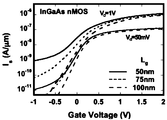
- FIG. 19 is a graph showing the gate voltage vs. source current characteristics, and shows the data for the nMOSFE on the InGaAs crystal layer when the gate length Lg is made smaller than that shown in FIG. Although the off-current increases due to the short channel effect and the subthreshold characteristic (SS value) deteriorates, the switching characteristic is observed even when the gate length is 50 nm.
- SS value subthreshold characteristic
- FIG. 20 is a graph showing the SS value with respect to the gate length
- FIG. 21 is a graph showing a DIBL (drain-induced barrier lowering) value with respect to the gate length.
- 100 semiconductor device 102 base substrate, 103 bonding surface, 104 first semiconductor crystal layer, 104a part of first semiconductor crystal layer, 106 second semiconductor crystal layer, 106a part of second semiconductor crystal layer, 108 first separation Layer, 110 second separation layer, 112 conductive material layer, 114 insulating layer, 114a part of insulating layer, 120 first MISFET, 122 first gate, 123 first gate metal, 124 first source, 125 first source electrode 126, first drain, 127, first drain electrode, 130, second MISFET, 132, second gate, 133, second gate metal, 134, second source, 135, second source electrode, 136, second drain, 137, second drain electrode, 140
Landscapes
- Thin Film Transistor (AREA)
- Metal-Oxide And Bipolar Metal-Oxide Semiconductor Integrated Circuits (AREA)
- Recrystallisation Techniques (AREA)
- Electrodes Of Semiconductors (AREA)
Abstract
第1半導体結晶層に形成された第1チャネル型の第1MISFETの第1ソースおよび第1ドレインと、第2半導体結晶層に形成された第2チャネル型の第2MISFETの第2ソースおよび第2ドレインが、同一の導電性物質からなり、当該導電性物質の仕事関数ΦMが、数1および数2の少なくとも一方の関係を満たす。 (数1) φ1<ΦM<φ2+Eg2 (数2) |ΦM-φ1|≦0.1eV、かつ、|(φ2+Eg2)-ΦM|≦0.1eV ただし、φ1は、N型半導体結晶層の電子親和力、φ2およびEg2は、P型半導体結晶層の電子親和力および禁制帯幅。
Description
本発明は、半導体デバイス、半導体基板、半導体基板の製造方法および半導体デバイスの製造方法に関する。なお本願は、平成22年度、独立行政法人新エネルギー・産業技術総合開発機構委託研究「ナノエレクトロニクス半導体新材料・新構造ナノ電子デバイス技術開発 ―シリコンプラットフォーム上III-V族半導体チャネルトランジスタ技術の研究開発」、産業技術力強化法第19条の適用を受ける特許出願である。
GaAs、InGaAs等のIII-V族化合物半導体は、高い電子移動度を有し、Ge、SiGe等のIV族半導体は、高い正孔移動度を有する。よって、III-V族化合物半導体でNチャネル型のMOSFET(Metal-Oxide-Semiconductor Field Effect Transistor)を構成し、IV族半導体でPチャネル型のMOSFETを構成すれば、高い性能を備えたCMOSFET(Complementary Metal-Oxide-Semiconductor Field Effect Transistor)が実現できる。非特許文献1には、III-V族化合物半導体をチャネルとするNチャネル型MOSFETとGeをチャネルとするPチャネル型MOSFETが、単一基板に形成されたCMOSFET構造が開示されている。
非特許文献1 S. Takagi, et al., SSE, vol. 51, pp. 526-536, 2007.
非特許文献1 S. Takagi, et al., SSE, vol. 51, pp. 526-536, 2007.
III-V族化合物半導体をチャネルとするNチャネル型MISFET(Metal-Insulator-Semiconductor Field-Effect Transistor)(以下単に「nMISFET」という。)と、IV族半導体をチャネルとするPチャネル型MISFET(以下単に「pMISFET」という。)とを、一つの基板上に形成するには、nMISFET用のIII-V族化合物半導体と、pMISFET用のIV族半導体を同一基板上に形成する技術が必要になる。LSI(Large Scale Integration)として製造することを考慮すれば、既存製造装置および既存工程の活用が可能なシリコン基板上にnMISFET用のIII-V族化合物半導体結晶層およびpMISFET用のIV族半導体結晶層を形成することが好ましい。
また、nMISFETとpMISFETとで構成されるCMISFET(Complementary Metal-Insulator-Semiconductor Field-Effect Transistor)を、LSIとして安価に効率よく製造するには、nMISFETおよびpMISFETが同時に形成される製造プロセスを採用することが好ましい。特に、nMISFETのソース・ドレインとpMISFETのソース・ドレインが同時に形成できれば、工程を簡略化することができ、コスト削減とともに素子の微細化にも容易に対応できるようになる。
たとえばnMISFETのソース・ドレイン形成領域とpMISFETのソース・ドレイン形成領域とに、ソースおよびドレインとなる材料を薄膜として形成し、さらにフォトリソグラフィ等によりパターニングして形成することで、nMISFETのソース・ドレインとpMISFETのソース・ドレインとを同時に形成できる。しかし、nMISFETが形成されるIII-V族化合物半導体結晶層と、pMISFETが形成されるIV族半導体結晶層とでは、構成される材料が異なる。このため、nMISFETまたはpMISFETの一方または両方のソース・ドレイン領域の抵抗が大きくなり、あるいは、nMISFETまたはpMISFETの一方または両方のソース・ドレイン領域とソース・ドレイン電極との接触抵抗が大きくなる。従って、nMISFETおよびpMISFETの両方のソース・ドレイン領域の抵抗あるいはソース・ドレイン電極との接触抵抗を小さくすることが難しい。
本発明の目的は、チャネルがIII-V族化合物半導体であるnMISFETと、チャネルがIV族半導体であるpMISFETと、で構成されるCMISFETを、一つの基板上に形成する場合において、nMISFETおよびpMISFETの各ソースおよび各ドレインを同時に形成し、かつ、ソース・ドレイン領域の抵抗またはソース・ドレイン電極との接触抵抗が小さくなるような半導体デバイスおよびその製造方法を提供することにある。また、そのような技術に適した半導体基板を提供することにある。
上記課題を解決するために、本発明の第1の態様においては、ベース基板と、ベース基板の上方に位置する第1半導体結晶層と、第1半導体結晶層における一部の領域の上方に位置する第2半導体結晶層と、第2半導体結晶層が上方に位置しない第1半導体結晶層の領域の一部をチャネルとし、第1ソースおよび第1ドレインを有する第1MISFETと、第2半導体結晶層の一部をチャネルとし、第2ソースおよび第2ドレインを有する第2MISFETと、を有し、第1MISFETが、第1チャネル型のMISFETであり、第2MISFETが、第1チャネル型とは相違する第2チャネル型のMISFETであり、第1ソース、第1ドレイン、第2ソースおよび第2ドレインが、同一の導電性物質からなり、導電性物質の仕事関数ΦMが、数1および数2の少なくとも一方の関係を満たす半導体デバイスを提供する。
(数1) φ1<ΦM<φ2+Eg2
(数2) |ΦM-φ1|≦0.1eV、かつ、|(φ2+Eg2)-ΦM|≦0.1eV
(数1) φ1<ΦM<φ2+Eg2
(数2) |ΦM-φ1|≦0.1eV、かつ、|(φ2+Eg2)-ΦM|≦0.1eV
ただし、φ1は、第1半導体結晶層および第2半導体結晶層のうち、一部がN型チャネルとして機能するほうの半導体結晶層を構成する結晶の電子親和力、φ2およびEg2は、第1半導体結晶層および第2半導体結晶層のうち、一部がP型チャネルとして機能するほうの半導体結晶層を構成する結晶の電子親和力および禁制帯幅を示す。
ベース基板と第1半導体結晶層との間に位置し、ベース基板と第1半導体結晶層とを電気的に分離する第1分離層と、第1半導体結晶層と第2半導体結晶層との間に位置し、第1半導体結晶層と第2半導体結晶層とを電気的に分離する第2分離層と、をさらに有してもよい。
第1半導体結晶層と第2半導体結晶層との間に位置し、第1半導体結晶層と第2半導体結晶層とを電気的に分離する第2分離層をさらに有してもよく、この場合、ベース基板と第1半導体結晶層とが接合面で接し、接合面の近傍におけるベース基板の領域に、p型またはn型の伝導型を示す不純物原子を含有し、接合面の近傍における第1半導体結晶層の領域に、ベース基板に含有された不純物原子が示す伝導型とは異なる伝導型を示す不純物原子を含有してもよい。
ベース基板と第1分離層とが接してもよく、この場合、ベース基板の第1分離層と接する領域が導電性であり、ベース基板の第1分離層と接する領域に印加した電圧が、第1MISFETへのバックゲート電圧として作用してもよい。第1半導体結晶層と第2分離層とが接してもよく、この場合、第1半導体結晶層の第2分離層と接する領域が導電性であり、第1半導体結晶層の第2分離層と接する領域に印加した電圧が、第2MISFETへのバックゲート電圧として作用してもよい。
第1半導体結晶層がIV族半導体結晶からなる場合、第1MISFETがPチャネル型MISFETであることが好ましく、第2半導体結晶層がIII-V族化合物半導体結晶からなる場合、第2MISFETがNチャネル型MISFETであることが好ましい。第1半導体結晶層がIII-V族化合物半導体結晶からなる場合、第1MISFETがNチャネル型MISFETであることが好ましく、第2半導体結晶層がIV族半導体結晶からなる場合、第2MISFETがPチャネル型MISFETであることが好ましい。
導電性物質として、TiN、TaN、グラフェン、HfNまたはWNが挙げられる。
本発明の第2の態様においては、第1の態様の半導体デバイスに用いる半導体基板であって、ベース基板と、第1半導体結晶層と、第2半導体結晶層と、を有し、第1半導体結晶層が、ベース基板の上方に位置し、第2半導体結晶層が、第1半導体結晶層の一部または全部の上方に位置する半導体基板を提供する。
ベース基板と第1半導体結晶層との間に位置し、ベース基板と第1半導体結晶層とを電気的に分離する第1分離層と、第1半導体結晶層と第2半導体結晶層との間に位置し、第1半導体結晶層と第2半導体結晶層とを電気的に分離する第2分離層と、をさらに有してもよい。この場合、第1分離層として、非晶質絶縁体からなるものが挙げられる。あるいは、第1分離層として、第1半導体結晶層を構成する半導体結晶の禁制帯幅より大きな禁制帯幅を有する半導体結晶からなるものが挙げられる。
第1半導体結晶層と第2半導体結晶層との間に位置し、第1半導体結晶層と第2半導体結晶層とを電気的に分離する第2分離層をさらに有してもよく、この場合、ベース基板と第1半導体結晶層とが接合面で接し、接合面の近傍におけるベース基板の領域に、p型またはn型の伝導型を示す不純物原子を含有し、接合面の近傍における第1半導体結晶層の領域に、ベース基板に含有された不純物原子が示す伝導型とは異なる伝導型を示す不純物原子を含有してもよい。
第2分離層として、非晶質絶縁体からなるものが挙げられる。あるいは、第2分離層として、第2半導体結晶層を構成する半導体結晶の禁制帯幅より大きな禁制帯幅を有する半導体結晶からなるものが挙げられる。第2半導体結晶層を複数有してもよく、この場合、複数の第2半導体結晶層のそれぞれが、ベース基板の上面と平行な面内で規則的に配列されていることが好ましい。
本発明の第3の態様においては、第2の態様の半導体基板を製造する方法であって、ベース基板の上方に第1半導体結晶層を形成する第1半導体結晶層形成ステップと、第1半導体結晶層における一部の領域の上方に第2半導体結晶層を形成する第2半導体結晶層形成ステップと、を有し、第2半導体結晶層形成ステップが、半導体結晶層形成基板上に第2半導体結晶層をエピタキシャル結晶成長法により形成するエピタキシャル成長ステップと、第1半導体結晶層の上、第2半導体結晶層の上、または、第1半導体結晶層および第2半導体結晶層の両方の上に、第1半導体結晶層と第2半導体結晶層とを電気的に分離する第2分離層を形成するステップと、第1半導体結晶層上の第2分離層と第2半導体結晶層とが接合するように、第2半導体結晶層上の第2分離層と第1半導体結晶層とが接合するように、または、第1半導体結晶層上の第2分離層と第2半導体結晶層上の第2分離層とが接合するように、第1半導体結晶層を有するベース基板と、半導体結晶層形成基板とを貼り合わせる貼り合わせステップと、を有する半導体基板の製造方法を提供する。
第1半導体結晶層形成ステップが、半導体結晶層形成基板上に第1半導体結晶層をエピタキシャル結晶成長法により形成するエピタキシャル成長ステップと、ベース基板の上、第1半導体結晶層の上、または、ベース基板および第1半導体結晶層の両方の上に、ベース基板と第1半導体結晶層とを電気的に分離する第1分離層を形成するステップと、ベース基板上の第1分離層と第1半導体結晶層とが接合するように、第1半導体結晶層上の第1分離層とベース基板とが接合するように、または、ベース基板上の第1分離層と第1半導体結晶層上の第1分離層とが接合するように、ベース基板と、半導体結晶層形成基板とを貼り合わせる貼り合わせステップと、を有してもよい。
第1半導体結晶層がSiGeからなり、第2半導体結晶層がIII-V族化合物半導体結晶からなる場合、第1半導体結晶層形成ステップの前に、絶縁体からなる第1分離層をベース基板の上に形成するステップを有してもよく、第1半導体結晶層形成ステップが、第1分離層の上に、第1半導体結晶層の出発材料となるSiGe層を形成するステップと、SiGe層を酸化雰囲気中で加熱し、表面を酸化することでSiGe層中のGe原子の濃度を高めるステップと、を有してもよい。
第1半導体結晶層がIV族半導体結晶からなり、第2半導体結晶層がIII-V族化合物半導体結晶からなる場合、IV族半導体結晶からなる半導体層材料基板の表面に、絶縁体からなる第1分離層を形成するステップと、第1分離層を通して、陽イオンを半導体層材料基板の分離予定深さに注入するステップと、第1分離層の表面とベース基板の表面とが接合されるように、半導体層材料基板とベース基板とを貼り合わせるステップと、半導体層材料基板およびベース基板を加熱し、分離予定深さに注入した陽イオンと半導体層材料基板を構成するIV族原子とを反応させることで、分離予定深さに位置するIV族半導体結晶を変性するステップと、変性するステップで変性させたIV族半導体結晶の変性部位よりベース基板側に位置するIV族半導体結晶を、半導体層材料基板とベース基板とを分離することで半導体層材料基板から剥離するステップと、ベース基板に残留したIV族半導体結晶からなる結晶層を研磨するステップと、を有してもよい。
第1半導体結晶層形成ステップの前に、ベース基板の上に第1半導体結晶層を構成する半導体結晶の禁制帯幅より大きな禁制帯幅を有する半導体結晶からなる第1分離層をエピタキシャル成長法により形成するステップを有してもよく、この場合、第1半導体結晶層形成ステップとして、第1分離層の上に第1半導体結晶層をエピタキシャル成長法により形成するステップが挙げられる。
第1半導体結晶層形成ステップとして、ベース基板の上に第1半導体結晶層をエピタキシャル成長法により形成するステップが挙げられる。この場合、ベース基板の表面近傍に、p型またはn型の伝導型を示す不純物原子を含有してもよく、第1半導体結晶層をエピタキシャル成長法により形成するステップにおいて、ベース基板に含有された不純物原子が示す伝導型とは異なる伝導型を示す不純物原子で第1半導体結晶層をドープしてもよい。
本発明の第4の態様においては、第2の態様の半導体基板を製造する方法であって、半導体結晶層形成基板の上に第2半導体結晶層をエピタキシャル結晶成長法により形成する第2半導体結晶層形成ステップと、第2半導体結晶層の上に、第2半導体結晶層を構成する半導体結晶の禁制帯幅より大きな禁制帯幅を有する半導体結晶からなる第2分離層をエピタキシャル結晶成長法により形成する第2分離層形成ステップと、第2分離層の上に第1半導体結晶層をエピタキシャル結晶成長法により形成する第1半導体結晶層形成ステップと、ベース基板の上、第1半導体結晶層の上、または、ベース基板および第1半導体結晶層の両方の上に、ベース基板と第1半導体結晶層とを電気的に分離する第1分離層を形成するステップと、ベース基板上の第1分離層と第1半導体結晶層とが接合するように、第1半導体結晶層上の第1分離層とベース基板とが接合するように、または、ベース基板上の第1分離層と第1半導体結晶層上の第1分離層とが接合するように、ベース基板と、半導体結晶層形成基板とを貼り合わせる貼り合わせステップと、を有する半導体基板の製造方法を提供する。
上記した第3態様および第4態様の半導体基板の製造方法において、半導体結晶層形成基板の上に半導体結晶層を形成する前に、半導体結晶層形成基板の表面に、結晶性犠牲層をエピタキシャル結晶成長法により形成するステップと、ベース基板と前導体結晶層形成基板とを貼り合わせた後に、結晶性犠牲層を除去することにより、半導体結晶層形成基板上にエピタキシャル結晶成長法により形成された半導体結晶層と半導体結晶層形成基板とを分離するステップと、をさらに有してもよい。第2半導体結晶層をエピタキシャル成長させた後に第2半導体結晶層を規則的な配列にパターニングするステップ、または第2半導体結晶層を予め規則的な配列に選択的にエピタキシャル成長させるステップ、のいずれかのステップを有してもよい。
本発明の第5の態様においては、第3の態様または第4の態様の半導体基板の製造方法を用いて、第1半導体結晶層および第2半導体結晶層を有する半導体基板を製造するステップと、第1半導体結晶層および第2半導体結晶層のそれぞれの上に、仕事関数ΦMが、数1および数2の少なくとも一方の関係を満たす導電性物質を形成するステップと、ゲート電極が形成される領域の導電性物質を除去するステップと、導電性物質が除去された領域にゲート絶縁層およびゲート電極を形成するステップと、導電性物質をパターニングおよび加熱して、第1半導体結晶上のゲート電極の両側に第1ソースおよび第1ドレインを形成し、第2半導体結晶上のゲート電極の両側に第2ソースおよび第2ドレインを形成するステップと、を有する半導体デバイスの製造方法を提供する。
(数1) φ1<ΦM<φ2+Eg2
(数2) |ΦM-φ1|≦0.1eV、かつ、|(φ2+Eg2)-ΦM|≦0.1eV
(数1) φ1<ΦM<φ2+Eg2
(数2) |ΦM-φ1|≦0.1eV、かつ、|(φ2+Eg2)-ΦM|≦0.1eV
ただし、φ1は、第1半導体結晶層および第2半導体結晶層のうち、一部がN型チャネルとして機能する半導体結晶層を構成する結晶の電子親和力、φ2およびEg2は、第1半導体結晶層および第2半導体結晶層のうち、一部がP型チャネルとして機能する半導体結晶層を構成する結晶の電子親和力および禁制帯幅を示す。
図1は、半導体デバイス100の断面を示す。半導体デバイス100は、ベース基板102と、第1半導体結晶層104と、第2半導体結晶層106とを有する。本例の半導体デバイス100は、ベース基板102と第1半導体結晶層104との間に第1分離層108を有し、第1半導体結晶層104と第2半導体結晶層106との間に第2分離層110を有する。なお、図1に示した実施例からは、ベース基板102と、第1半導体結晶層104と、第2半導体結晶層106とを構成要件とする半導体基板の発明と、ベース基板102、第1分離層108、第1半導体結晶層104、第2分離層110および第2半導体結晶層106を構成要件とする半導体基板の発明との少なくとも2つの発明が把握できる。第1半導体結晶層104には第1MISFET120が形成され、第2半導体結晶層106には第2MISFET130が形成されている。
ベース基板102として、表面がシリコン結晶である基板が挙げられる。表面がシリコン結晶である基板として、シリコン基板、または、SOI(Silicon on Insulator)基板が挙げられ、シリコン基板が好ましい。ベース基板102に、表面がシリコン結晶である基板を用いることで、既存の製造装置および既存の製造プロセスが利用でき、研究開発および製造の効率を高めることができる。ベース基板102は、表面がシリコン結晶である基板に限られず、ガラス、セラミックス、プラスティック等の絶縁体基板、金属等の導電体基板、または、炭化シリコン等の半導体基板であってもよい。
第1半導体結晶層104は、ベース基板102の上方に位置する。第1半導体結晶層104は、IV族半導体結晶またはIII-V族化合物半導体結晶からなる。第1半導体結晶層104の厚さは、20nm以下であることが好ましい。第1半導体結晶層104の厚さを20nm以下とすることで、極薄膜ボディの第1MISFET120を構成できる。第1MISFET120のボディを極薄膜にすることで、短チャネル効果を抑制し、第1MISFET120のリーク電流を減少することができる。
第2半導体結晶層106は、第1半導体結晶層104表面の一部の上方に位置する。すなわち、第2半導体結晶層106は、第1半導体結晶層104における一部の領域の上方に位置し、第1半導体結晶層104の領域のうち、第2半導体結晶層106が上方に位置しない領域の一部は、第1MISFET120のチャネルとして機能する。第2半導体結晶層106は、III-V族化合物半導体結晶またはIV族半導体結晶からなる。第2半導体結晶層106の厚さは、20nm以下であることが好ましい。第2半導体結晶層106の厚さを20nm以下とすることで、極薄膜ボディの第2MISFET130を構成できる。第2MISFET130のボディを極薄膜にすることで、短チャネル効果を抑制し、第2MISFET130のリーク電流を減少することができる。
III-V族化合物半導体結晶では電子移動度が高く、IV族半導体結晶、特にGeでは正孔移動度が高いので、III-V族化合物半導体結晶層にはNチャネル型MISFETを形成することが好ましく、IV族半導体結晶層にはPチャネル型MISFETを形成することが好ましい。つまり、第1半導体結晶層104がIV族半導体結晶からなり、第2半導体結晶層106がIII-V族化合物半導体結晶からなる場合、第1MISFET120がPチャネル型MISFETであり、第2MISFET130がNチャネル型MISFETであることが好ましい。
逆に、第1半導体結晶層104がIII-V族化合物半導体結晶からなり、第2半導体結晶層106がIV族半導体結晶からなる場合、第1MISFET120がNチャネル型MISFETであり、第2MISFET130がPチャネル型MISFETであることが好ましい。これにより、第1MISFET120および第2MISFET130の各々の性能を高め、第1MISFET120および第2MISFET130からなるCMISFETの性能を最大化することができる。
IV族半導体結晶として、Ge結晶、または、SixGe1-x(0≦x<1)結晶、が挙げられる。IV族半導体結晶がSixGe1-x結晶である場合、xは0.10以下であることが好ましい。III-V族化合物半導体結晶として、InxGa1-xAs(0<x<1)結晶、InAs結晶、GaAs結晶、InP結晶が挙げられる。また、III-V族化合物半導体結晶として、GaAsまたはInPに格子整合または擬格子整合するIII-V族化合物半導体の混晶が挙げられる。また、III-V族化合物半導体結晶として、当該混晶とInxGa1-xAs(0<x<1)結晶、InAs結晶、GaAs結晶またはInP結晶との積層体が挙げられる。なおIII-V族化合物半導体結晶としては、InxGa1-xAs(0<x<1)結晶およびInAs結晶が好適であり、InAs結晶がより好適である。
第1分離層108は、ベース基板102と第1半導体結晶層104との間に位置する。第1分離層108は、ベース基板102と第1半導体結晶層104とを電気的に分離する。
第1分離層108は、非晶質絶縁体からなるものであってもよい。第1半導体結晶層104および第1分離層108が、貼り合わせ法、酸化濃縮法またはスマートカット法により形成された場合、第1分離層108は非晶質絶縁体からなる。非晶質絶縁体からなる第1分離層108として、Al2O3、AlN、Ta2O5、ZrO2、HfO2、La2O3、SiOx(例えばSiO2)、SiNx(例えばSi3N4)およびSiOxNyのうちの少なくとも1からなる層、またはこれらの中から選ばれた少なくとも2層の積層が挙げられる。
第1分離層108は、第1半導体結晶層104を構成する半導体結晶の禁制帯幅より大きな禁制帯幅を有する半導体結晶からなるものであってもよい。このような半導体結晶は、エピタキシャル結晶成長法により形成できる。第1半導体結晶層104がInGaAs結晶層またはGaAs結晶層である場合、第1分離層108を構成する半導体結晶として、AlGaAs結晶、AlInGaP結晶、AlGaInAs結晶、InP結晶が挙げられる。第1半導体結晶層104がGe結晶層である場合、第1分離層108を構成する半導体結晶として、SiGe結晶、Si結晶、SiC結晶、または、C結晶が挙げられる。
第2分離層110は、第1半導体結晶層104と第2半導体結晶層106との間に位置する。第2分離層110は、第1半導体結晶層104と第2半導体結晶層106とを電気的に分離する。
第2分離層110は、非晶質絶縁体からなるものであってもよい。第2半導体結晶層106および第2分離層110が貼り合わせ法により形成された場合、第2分離層110は、非晶質絶縁体になる。非晶質絶縁体からなる第2分離層110として、Al2O3、AlN、Ta2O5、ZrO2、HfO2、La2O3、SiOx(例えばSiO2)、SiNx(例えばSi3N4)およびSiOxNyのうちの少なくとも1からなる層、またはこれらの中から選ばれた少なくとも2層の積層が挙げられる。
第2分離層110は、第2半導体結晶層106を構成する半導体結晶の禁制帯幅より大きな禁制帯幅を有する半導体結晶からなるものであってもよい。このような半導体結晶は、エピタキシャル結晶成長法により形成できる。第2半導体結晶層106がInGaAs結晶層またはGaAs結晶層である場合、当該半導体結晶として、AlGaAs結晶、AlInGaP結晶、AlGaInAs結晶、InP結晶が挙げられる。第2半導体結晶層106がGe結晶層である場合、当該半導体結晶として、SiGe結晶、Si結晶、SiC結晶、C結晶が挙げられる。
第1MISFET120は、第2半導体結晶層106が上方に位置しない領域の第1半導体結晶層104に形成され、第1ゲート122、第1ソース124および第1ドレイン126を有する。第1ゲート122上には、第1ゲートメタル123が形成され、第1ソース124および第1ドレイン126のそれぞれの上には、第1ソース電極125、第1ドレイン電極127がそれぞれ形成されている。第1ゲートメタル123、第1ソース電極125および第1ドレイン電極127を構成する物質として、Ti、Ta、W、Al、Cu、Auまたはこれらの積層体が挙げられる。
第1ソース124および第1ドレイン126は、第1半導体結晶層104上に形成された導電性物質からなり、レイズド・ソース・ドレインを成す。導電性物質として、TiN、TaN、グラフェン、HfNまたはWNが挙げられる。第1ソース124および第1ドレイン126の間には、第1ゲート122が形成されている。第1ゲート122は、絶縁層114によって、第1ソース124、第1ドレイン126および第1半導体結晶層104から絶縁されている。第1ゲート122を構成する物質として、TiN、TaN、グラフェン、HfNまたはWNが挙げられる。絶縁層114として、Al2O3、AlN、Ta2O5、ZrO2、HfO2、La2O3、SiOx(例えばSiO2)、SiNx(例えばSi3N4)およびSiOxNyのうちの少なくとも1からなる層、またはこれらの中から選ばれた少なくとも2層の積層が挙げられる。
第1ソース124と第1ドレイン126との間の、第1ゲート122が絶縁層114を介して対面している第1半導体結晶層104の一部104aは、第1MISFET120のチャネルとして機能する。当該チャネル領域である第1半導体結晶層104の一部104aと第1ゲート122とで挟まれた領域には、絶縁層114の一部114aが形成される。当該一部114aは、ゲート絶縁層として機能してもよい。
第2MISFET130は、第2半導体結晶層106に形成され、第2ゲート132、第2ソース134および第2ドレイン136を有する。第2ゲート132上には、第2ゲートメタル133が形成され、第2ソース134および第2ドレイン136のそれぞれの上には、第2ソース電極135、第2ドレイン電極137がそれぞれ形成されている。第2ゲートメタル133、第2ソース電極135および第2ドレイン電極137を構成する物質として、Ti、Ta、W、Al、Cu、Auおよびこれらの積層体が挙げられる。
第2ソース134および第2ドレイン136は、第2半導体結晶層106上に形成された導電性物質からなり、レイズド・ソース・ドレインを成す。導電性物質として、TiN、TaN、グラフェン、HfNまたはWNが挙げられる。第2ソース134および第2ドレイン136の間には、第2ゲート132が形成されている。第2ゲート132は、第1MISFET120と同様の絶縁層114によって、第2ソース134、第2ドレイン136および第2半導体結晶層106から絶縁されている。第2ゲート132を構成する物質として、TiN、TaN、グラフェン、HfNまたはWNが挙げられる。
第2ソース134と第2ドレイン136との間の、第2ゲート132が絶縁層114を介して対面している第2半導体結晶層106の一部106aは、第2MISFET130のチャネルとして機能する。当該チャネル領域である第2半導体結晶層106の一部106aと第2ゲート132とで挟まれた領域には、絶縁層114の一部114aが形成される。当該一部114aは、ゲート絶縁層として機能してもよい。
第1ソース124、第1ドレイン126、第2ソース134および第2ドレイン136は、同一の導電性物質からなり、導電性物質の仕事関数ΦMは、数1または数2の関係を満たす。
(数1) φ1<ΦM<φ2+Eg2
(数2) |ΦM-φ1|≦0.1eV、かつ、|(φ2+Eg2)-ΦM|≦0.1eV
(数1) φ1<ΦM<φ2+Eg2
(数2) |ΦM-φ1|≦0.1eV、かつ、|(φ2+Eg2)-ΦM|≦0.1eV
ただし、φ1は、第1半導体結晶層104および第2半導体結晶層106のうち、一部がN型チャネルとして機能するほうの半導体結晶層を構成する結晶の電子親和力を示す。φ2およびEg2は、第1半導体結晶層104および第2半導体結晶層106のうち、一部がP型チャネルとして機能するほうの半導体結晶層を構成する結晶の電子親和力および禁制帯幅を示す。なお、導電性物質の仕事関数ΦMは、数1および数2の両方の関係を満たしてもよい。
以上の通り、第1MISFET120のソース・ドレイン(第1ソース124および第1ドレイン126)と、第2MISFET130のソース・ドレイン(第2ソース134および第2ドレイン136)が、同一の導電性物質からなる。これは同一の材料膜を用いた当該部位の製造を可能にする構成であり、製造工程を簡略化できることを意味する。また、第1MISFET120および第2MISFET130において、ゲート幅は、ソース・ドレイン間のスペース(エッチング溝間隔)によって容易に制御できる。この結果、微細化が容易になる。また、第1ソース124、第1ドレイン126、第2ソース134および第2ドレイン136を構成する導電物質の仕事関数を、上記数1または数2の関係を満たすものとするので、各ソース・ドレイン領域と半導体結晶層との接触抵抗を低減できる。例えば、導電性物質の仕事関数ΦMが、数1の関係を満たせば、ΦMとφ1との差分、および、ΦMとφ2+Eg2との差分は、最大でもφ1とφ2+Eg2との差分よりも小さくなる。各ソース・ドレイン領域と半導体結晶層との接触抵抗を低減できる。また、導電性物質の仕事関数ΦMが、数2の関係を満たせば、ΦMとφ1との差分、および、ΦMとφ2+Eg2との差分を、0.1eV以下に抑制できる。このため、各ソース・ドレイン領域と半導体結晶層との接触抵抗を低減できる。この結果、CMISFETを製造する製造工程を簡略化し、微細化を容易にすると共に各FETの性能を高くすることができる。
図2から図8は、半導体デバイス100の製造過程における断面を示す。まず、ベース基板102と半導体結晶層形成基板140を用意し、半導体結晶層形成基板140上に第1半導体結晶層104をエピタキシャル結晶成長法により形成する。その後、第1半導体結晶層104上に第1分離層108を形成する。第1分離層108は、たとえばALD(Atomic Layer Deposition)法、熱酸化法、蒸着法、CVD(Chemical Vapor Deposition)法、スパッタ法等の薄膜形成法により形成する。
第1半導体結晶層104がIII-V族化合物半導体結晶からなる場合、半導体結晶層形成基板140としてInP基板、または、GaAs基板が選択できる。第1半導体結晶層104がIV族半導体結晶からなる場合、半導体結晶層形成基板140としてGe基板、Si基板、SiC基板、または、GaAs基板が選択できる。
第1半導体結晶層104のエピタキシャル結晶成長には、MOCVD(Metal Organic Chemical Vapor Deposition)法を利用することができる。III-V族化合物半導体結晶層をMOCVD法で形成する場合、InソースにはTMIn(トリメチルインジウム)を、GaソースにはTMGa(トリメチルガリウム)を、AsソースにはAsH3(アルシン)、PソースにはPH3(ホスフィン)を用いることができる。キャリアガスには水素を用いることができる。反応温度は、300℃から900℃の範囲で、好ましくは450~750℃の範囲で適宜選択できる。IV族半導体結晶層をCVD法で形成する場合、Geソースには、GeH4(ゲルマン)を、SiソースにはSiH4(シラン)、またはSi2H6(ジシラン)を用いることができ、またそれらの複数の水素原子の一部を塩素原子または炭化水素基で置換した化合物を用いることもできる。キャリアガスには水素を用いることができる。反応温度は、300℃から900℃の範囲で、好ましくは450~750℃の範囲で適宜選択できる。ソースガス供給量や反応時間を適宜選択することでエピタキシャル成長層の厚さを制御することができる。
図2に示すように、第1分離層108の表面とベース基板102の表面をアルゴンビーム150で活性化する。その後、図3に示すように、アルゴンビーム150で活性化した第1分離層108の表面とベース基板102の表面を貼り合わせて接合する。貼り合わせは室温で行うことができる。なお、活性化はアルゴンビーム150である必要はなく、他の希ガス等のビームであっても良い。その後、半導体結晶層形成基板140をエッチングし、除去する。これにより、ベース基板102上に、第1分離層108および第1半導体結晶層104が形成される。なお、第1半導体結晶層104の形成と第1分離層108の形成との間に、第1半導体結晶層104の表面を硫黄原子で終端する硫黄終端処理を行っても良い。
図2および図3に示す例では、第1分離層108を第1半導体結晶層104の上にのみ形成し、第1分離層108の表面とベース基板102の表面とを貼り合わせる例を説明したが、ベース基板102の上にも第1分離層108を形成し、第1半導体結晶層104上の第1分離層108の表面とベース基板102上の第1分離層108の表面とを貼り合わせてもよい。この場合、第1分離層108の貼り合わせる面を親水化処理することが好ましい。親水化処理した場合は、第1分離層108どうしを加熱して貼り合わせることが好ましい。あるいは、ベース基板102の上にのみ第1分離層108を形成し、第1半導体結晶層104の表面とベース基板102上の第1分離層108の表面とを貼り合わせてもよい。
図2および図3に示す例では、第1分離層108および第1半導体結晶層104をベース基板102に貼り合わせた後に、第1分離層108および第1半導体結晶層104を半導体結晶層形成基板140から分離する例を説明したが、第1分離層108および第1半導体結晶層104を半導体結晶層形成基板140から分離した後に、第1分離層108および第1半導体結晶層104をベース基板102に貼り合わせてもよい。この場合、第1分離層108および第1半導体結晶層104を半導体結晶層形成基板140から分離した後、ベース基板102に貼り合わせるまでの間、適切な転写用基板に第1分離層108および第1半導体結晶層104を保持することが好ましい。
次に、半導体結晶層形成基板160を用意し、半導体結晶層形成基板160上に第2半導体結晶層106をエピタキシャル結晶成長法により形成する。また、ベース基板102上の第1半導体結晶層104の上に、第2分離層110を形成する。第2分離層110は、たとえばALD法、熱酸化法、蒸着法、CVD法、スパッタ法等の薄膜形成法により形成する。なお、第2分離層110の形成前に、第1半導体結晶層104の表面を硫黄原子で終端する硫黄終端処理を行っても良い。
第2半導体結晶層106がIII-V族化合物半導体結晶からなる場合、半導体結晶層形成基板160としてInP基板、または、GaAs基板が選択できる。第2半導体結晶層106がIV族半導体結晶からなる場合、半導体結晶層形成基板160としてGe基板、Si基板、SiC基板、または、GaAs基板が選択できる。
第2半導体結晶層106のエピタキシャル結晶成長には、MOCVD法を利用することができる。MOCVD法で用いるガス、反応温度の条件等は、第1半導体結晶層104の場合と同様である。
図4に示すように、第2半導体結晶層106の表面と第2分離層110の表面をアルゴンビーム150で活性化する。その後、図5に示すように、第2半導体結晶層106の表面を第2分離層110の表面の一部に貼り合わせて接合する。貼り合わせは室温で行うことができる。活性化はアルゴンビーム150である必要はなく、他の希ガス等のビームであっても良い。その後、半導体結晶層形成基板160をHCl溶液等でエッチングし、除去する。これにより、ベース基板102上の第1半導体結晶層104上に第2分離層110が形成され、第2分離層110表面の一部の上に第2半導体結晶層106が形成される。なお、第2分離層110と第1半導体結晶層104とを貼り合わせる前に、第2半導体結晶層106の表面を硫黄原子で終端する硫黄終端処理を行っても良い。
図4に示す例では、第2分離層110を第1半導体結晶層104の上にのみ形成し、第2分離層110の表面と第2半導体結晶層106の表面とを貼り合わせる例を説明したが、第2半導体結晶層106の上にも第2分離層110を形成し、第1半導体結晶層104上の第2分離層110の表面と第2半導体結晶層106上の第2分離層110の表面とを貼り合わせてもよい。この場合、第2分離層110の貼り合わせる面を親水化処理することが好ましい。親水化処理した場合は、第2分離層110どうしを加熱して貼り合わせることが好ましい。あるいは、第2半導体結晶層106の上にのみ第2分離層110を形成し、第1半導体結晶層104の表面と第2半導体結晶層106上の第2分離層110の表面とを貼り合わせてもよい。
図4に示す例では、第2半導体結晶層106をベース基板102上の第2分離層110に貼り合わせた後に、第2半導体結晶層106を半導体結晶層形成基板160から分離する例を説明したが、第2半導体結晶層106を半導体結晶層形成基板160から分離した後に、第2半導体結晶層106を第2分離層110に貼り合わせてもよい。この場合、第2半導体結晶層106を半導体結晶層形成基板160から分離した後、第2分離層110に貼り合わせるまでの間、適切な転写用基板に第2半導体結晶層106を保持することが好ましい。
次に、図6に示すように、第1半導体結晶層104および第2半導体結晶層106の上に、導電性物質層112を形成する。導電性物質層112は、後に第1ソース124、第1ドレイン126、第2ソース134および第2ドレイン136となるものである。導電性物質層112は、たとえば蒸着法、CVD法、スパッタ法等の薄膜形成法により形成する。なお、図6においては、第2分離層110および第2半導体結晶層106の厚みにより、第1MISFET120および第2MISFET130の領域における導電性物質層112が分離している。他の例では、導電性物質層112の一部をエッチングする等の方法で、導電性物質層112を、第1MISFET120および第2MISFET130の領域に分離させてもよい。
図7に示すように、第1ゲート122および第2ゲート132が形成される領域の導電性物質層112を、エッチングにより除去して開口を形成する。その後、導電性物質層112および開口内部に絶縁層114を形成する。絶縁層114は、たとえばALD法、熱酸化法、蒸着法、CVD法、スパッタ法等の薄膜形成法により形成する。
図8に示すように、絶縁層114の上に、導電性薄膜を形成し、第1ゲート122および第2ゲート132となる領域以外の導電性薄膜を除去して、第1ゲート122および第2ゲート132を形成する。なお、第1ゲート122あるいは第2ゲート132で分離された導電性物質層112は、第1ソース124、第1ドレイン126、第2ソース134および第2ドレイン136となる。第1ソース124、第1ドレイン126、第2ソース134および第2ドレイン136となる導電性物質層112が露出するように絶縁層114に開口を形成し、導電性の薄膜形成およびパターニングにより第1ゲートメタル123、第1ソース電極125および第1ドレイン電極127、ならびに、第2ゲートメタル133、第2ソース電極135および第2ドレイン電極137を形成すれば、図1に示す半導体デバイス100が製造できる。なお、導電性薄膜として、金属膜を形成した場合には、ポストメタルアニール処理を行うことが好ましい。ポストメタルアニール処理は、RTA(rapid thermal annealing)法により実施することが好ましい。
以上説明した半導体デバイス100とその製造方法によれば、第1ソース124、第1ドレイン126、第2ソース134および第2ドレイン136が、同一プロセスで同時に形成されるので、製造工程を簡略化できる。その結果、製造コストが低減され、微細化も容易になる。また、第1ソース124、第1ドレイン126、第2ソース134および第2ドレイン136を構成する導電性物質の仕事関数が、数1または数2に示す関係を満足する。したがって第1ソース124および第1ドレイン126と第1半導体結晶層104とのコンタクトがオーミックコンタクトとなり、第2ソース134および第2ドレイン136と第2半導体結晶層106とのコンタクトがオーミックコンタクトとなる。この結果、第1MISFET120および第2MISFET130の各オン電流を大きくすることができる。また、各ソース・ドレイン間の抵抗が小さくなるから、各MISFETのチャネル抵抗を低くする必要がなく、チャネル層のドーピング不純物原子の濃度を少なくできる。この結果、チャネル層でのキャリアの移動度を大きくすることができる。
上記した半導体デバイス100では、ベース基板102と第1分離層108とが接しているので、ベース基板102の第1分離層108と接する領域が導電性であるならば、ベース基板102の第1分離層108と接する領域に電圧を印加し、当該電圧を、第1MISFET120へのバックゲート電圧として作用させることができる。また、上記した半導体デバイス100では、第1半導体結晶層104と第2分離層110とが接しているので、第1半導体結晶層104の第2分離層110と接する領域が導電性であるならば、第1半導体結晶層104の第2分離層110と接する領域に電圧を印加し、当該電圧を、第2MISFET130へのバックゲート電圧として作用させることができる。これらバックゲート電圧の作用は、第1MISFET120および第2MISFET130のオン電流を大きくし、オフ電流を小さくすることができる。
上記した半導体デバイス100において、第2半導体結晶層106を複数有し、複数の第2半導体結晶層106のそれぞれが、ベース基板102の上面と平行な面内で規則的に配列されてもよい。規則的とは、例えば同一の配列パターンが繰り返されることを指す。また、半導体デバイス100は、第1半導体結晶層104を複数有してもよく、複数の第1半導体結晶層104のそれぞれがベース基板102の上面と平行な面内で規則的に配列されてもよい。この場合、第1半導体結晶層104毎に、単一または複数の第2半導体結晶層106を有してもよく、それぞれの第2半導体結晶層106は、第1半導体結晶層104の上面と平行な面内で規則的に配列されてもよい。このように、第1半導体結晶層104あるいは第2半導体結晶層106を規則的に配列することで、半導体デバイス100に使用する半導体基板の生産性を高めることができる。第2半導体結晶層106または第1半導体結晶層104の規則的な配列は、第2半導体結晶層106または第1半導体結晶層104をエピタキシャル成長させた後に第2半導体結晶層106若しくは第1半導体結晶層104を規則的な配列にパターニングする方法、第2半導体結晶層106若しくは第1半導体結晶層104を予め規則的な配列に選択的にエピタキシャル成長させる方法、または第2半導体結晶層106若しくは第1半導体結晶層104のいずれかあるいは両方を、半導体結晶層形成基板160上にエピタキシャル成長させた後、半導体結晶層形成基板160から分離し、所定の形状に整形した後、規則的な配列でベース基板102上に貼り合せる方法、のいずれかの方法により実施でき、また、いずれか複数の方法を組み合わせた方法により実施できる。
上記した半導体デバイス100では、第1半導体結晶層104および第1分離層108を半導体結晶層形成基板140上に形成し、第1分離層108とベース基板102とを貼り合わせた後に半導体結晶層形成基板140を除去することで、第1半導体結晶層104および第1分離層108をベース基板102上に形成することを説明した。しかし、第1半導体結晶層104がSiGeからなり、第2半導体結晶層106がIII-V族化合物半導体結晶からなる場合、第1半導体結晶層104および第1分離層108は、酸化濃縮法により形成することもできる。すなわち、第1半導体結晶層104を形成する前に、絶縁体からなる第1分離層108をベース基板102の上に形成し、第1分離層108の上に、第1半導体結晶層104の出発材料となるSiGe層を形成する。SiGe層を酸化雰囲気中で加熱し、表面を酸化する。SiGe層を酸化することで、SiGe層中のGe原子の濃度を高め、Ge濃度が高い第1半導体結晶層104とすることができる。
あるいは、第1半導体結晶層104がIV族半導体結晶からなり、第2半導体結晶層106がIII-V族化合物半導体結晶からなる場合、第1半導体結晶層104および第1分離層108は、スマートカット法により形成できる。すなわち、IV族半導体結晶からなる半導体層材料基板の表面に、絶縁体からなる第1分離層108を形成し、第1分離層108を通して、陽イオンを半導体層材料基板の分離予定深さに注入する。第1分離層108の表面とベース基板102の表面とが接合されるように、半導体層材料基板とベース基板102とを貼り合わせ、半導体層材料基板およびベース基板102を加熱する。この加熱により、分離予定深さに注入した陽イオンと半導体層材料基板を構成するIV族原子とが反応し、分離予定深さに位置するIV族半導体結晶が変性する。この状態で半導体層材料基板とベース基板102とを分離すれば、IV族半導体結晶の変性部位よりベース基板102側に位置するIV族半導体結晶が、半導体層材料基板から剥離する。このベース基板102側に付着した半導体層材料に適切な研磨を施せば、研磨後の半導体結晶層を第1半導体結晶層104とすることができる。
上記した半導体デバイス100において、第1分離層108を、第1半導体結晶層104を構成する半導体結晶の禁制帯幅より大きな禁制帯幅を有する半導体結晶とする場合、ベース基板102の上に、第1分離層108をエピタキシャル成長法により形成し、第1分離層108の上に第1半導体結晶層104をエピタキシャル成長法により形成することができる。第1分離層108および第1半導体結晶層104を連続してエピタキシャル成長法により形成できるので、製造工程が簡単になる。
上記した半導体デバイス100において、第2分離層110を、第2半導体結晶層106を構成する半導体結晶の禁制帯幅より大きな禁制帯幅を有する半導体結晶とする場合、第2半導体結晶層106、第2分離層110および第1半導体結晶層104を連続してエピタキシャル成長法により形成できる。すなわち、図9に示すように、半導体結晶層形成基板180の上に第2半導体結晶層106をエピタキシャル結晶成長法により形成し、第2半導体結晶層106の上に、第2分離層110をエピタキシャル結晶成長法により形成し、第2分離層110の上に第1半導体結晶層104をエピタキシャル結晶成長法により形成する。これらエピタキシャル成長は連続して実施できる。第1半導体結晶層104の上に第1分離層108を形成し、第1分離層108の表面とベース基板102の表面をアルゴンビーム150で活性化する。その後、図10に示すように、第1分離層108の表面とベース基板102の表面を貼り合わせ、半導体結晶層形成基板180をHCl溶液等でエッチングし、除去する。さらに図11に示すように、マスク185を用いて第2半導体結晶層106の一部をエッチングし、図5と同様な半導体基板を得ることができる。当該方法であれば、第2半導体結晶層106、第2分離層110および第1半導体結晶層104を連続してエピタキシャル成長法により形成できるので、製造工程が簡単になる。
なお、図9および図10で説明した貼り合わせ工程において、図2および図3の場合と同様に、ベース基板102の上、および、第1半導体結晶層104の上の何れか一方または両方に第1分離層108を形成してもよい。また、第1分離層108、第1半導体結晶層104、第2分離層110および第2半導体結晶層106を適切な転写用基板に転写し、その後、ベース基板102に貼り合わせてもよい。さらに、第2分離層110がエピタキシャル成長結晶である場合、第1半導体結晶層104、第2分離層110および第2半導体結晶層106をベース基板102に貼り合わせた後、第2分離層110を酸化して非晶質絶縁体層に転換してもよい。たとえば、第2分離層110がAlAs、あるいはAlInPである場合、選択酸化技術により、第2分離層110を絶縁性酸化物とすることができる。
上記した半導体デバイス100の製造方法における貼り合わせ工程では、半導体結晶層形成基板をエッチングして除去する例を説明したが、図12に示すように、結晶性犠牲層190を用いて半導体結晶層形成基板を除去することもできる。すなわち、半導体結晶層形成基板140の上に第1半導体結晶層104を形成する前に、半導体結晶層形成基板140の表面に、結晶性犠牲層190をエピタキシャル結晶成長法により形成する。その後、結晶性犠牲層190の表面に第1半導体結晶層104および第1分離層108をエピタキシャル成長法により形成し、第1分離層108の表面とベース基板102の表面をアルゴンビーム150で活性化する。その後、第1分離層108の表面とベース基板102の表面を貼り合わせ、図13に示すように、結晶性犠牲層190を除去する。これにより、半導体結晶層形成基板140上の第1半導体結晶層104および第1分離層108と半導体結晶層形成基板140が分離される。当該方法によれば、半導体結晶層形成基板の再利用が可能になり、製造コストを低くすることができる。
図14は、半導体デバイス200の断面を示す。半導体デバイス200は、半導体デバイス100における第1分離層108を有さず、第1半導体結晶層104がベース基板102に接して配置されている。なお、第1分離層108が無い他は半導体デバイス100と同じ構造を有するので、共通する部材等の説明は省略する。
すなわち、半導体デバイス200は、ベース基板102と第1半導体結晶層104とが接合面103で接し、ベース基板102の接合面103の近傍に、p型またはn型の伝導型を示す不純物原子を含有し、第1半導体結晶層104の接合面103の近傍に、ベース基板102に含有された不純物原子が示す伝導型とは異なる伝導型を示す不純物原子を含有する。つまり、半導体デバイス200は、接合面103の近傍にpn接合を有する。第1分離層108が無い構造であっても、接合面103近傍に形成されるpn接合によって、ベース基板102と第1半導体結晶層104とを電気的に分離することが可能であり、第1半導体結晶層104に形成される第1MISFET120をベース基板102から電気的に分離することができる。
このようなpn接合による分離は、第1半導体結晶層104と第2半導体結晶層106との間においても適用できる。すなわち、第2分離層110が無く、第1半導体結晶層104と第2半導体結晶層106が接合面で接している構造において、第1半導体結晶層104の当該接合面の近傍に、p型またはn型の伝導型を示す不純物原子を含有し、第2半導体結晶層106の当該接合面の近傍に、第1半導体結晶層104に含有された不純物原子が示す伝導型とは異なる伝導型を示す不純物原子を含有する。これにより第1半導体結晶層104と第2半導体結晶層106を電気的に分離でき、第1半導体結晶層104に形成される第1MISFET120と第2半導体結晶層106に形成される第2MISFET130とを電気的に分離することができる。
なお、半導体デバイス200は、ベース基板102の上に第1半導体結晶層104をエピタキシャル成長法により形成し、第1半導体結晶層104の上に第2分離層110を形成する工程以降の工程を、半導体デバイス100の場合と同様の工程にすることで製造できる。ただし、pn接合の形成は、ベース基板102の表面近傍に、p型またはn型の伝導型を示す不純物原子を含有させ、第1半導体結晶層104をエピタキシャル成長法により形成するステップにおいて、ベース基板102に含有された不純物原子が示す伝導型とは異なる伝導型を示す不純物原子で第1半導体結晶層104をドープすることで実施できる。
第1半導体結晶層104をベース基板102の上に直接形成する構造において、素子分離の必要性が低い場合には分離構造としてのpn接合は必須ではない。つまり、半導体デバイス200は、ベース基板102の接合面103の近傍にp型またはn型の伝導型を示す不純物原子を含有せず、第1半導体結晶層104の接合面103の近傍にp型またはn型の伝導型を示す不純物原子を含有しない構造であってもよい。
第1半導体結晶層104をベース基板102の上に直接形成する場合、エピタキシャル成長の後、またはエピタキシャル成長の途中において、アニール処理を施してもよい。アニール処理により、第1半導体結晶層104中の転位が低減する。また、エピタキシャル成長法は、ベース基板102の表面全部に第1半導体結晶層104を一様に成長する方法、あるいは、SiO2等の成長阻害層でベース基板102の表面を細かく分割し、選択的に成長する方法の何れのエピタキシャル成長法であってもよい。
(実施例)
以下の実施例は、ベース基板表面の一部上方にGe結晶層を有し、Ge結晶層が上方に位置しないベース基板表面の他部上方にInGaAs結晶層を有する半導体基板を用いたものである。つまり、当該実施例は、ベース基板102上に第1半導体結晶層104を有し、第1半導体結晶層104上に第2半導体結晶層106を有する本発明の半導体基板とは構成が相違する。しかし、複数のソース・ドレインの製造工程を簡略化し、ゲートの微細化を容易にすると共に、各FETの性能を高くすることができるという観点では、以下の実施例の構成でも、図1に関連して説明した半導体デバイス100の構成でも同様の結果が得られる。例えば、本発明における第1半導体結晶層104および第2半導体結晶層106のそれぞれが、Ge結晶層およびInGaAs結晶層である場合、上述した観点においては、下記実施例と同様の結果が得られると推定できる。よって、本発明で期待される効果の一例として以下の実施例を説明する。
以下の実施例は、ベース基板表面の一部上方にGe結晶層を有し、Ge結晶層が上方に位置しないベース基板表面の他部上方にInGaAs結晶層を有する半導体基板を用いたものである。つまり、当該実施例は、ベース基板102上に第1半導体結晶層104を有し、第1半導体結晶層104上に第2半導体結晶層106を有する本発明の半導体基板とは構成が相違する。しかし、複数のソース・ドレインの製造工程を簡略化し、ゲートの微細化を容易にすると共に、各FETの性能を高くすることができるという観点では、以下の実施例の構成でも、図1に関連して説明した半導体デバイス100の構成でも同様の結果が得られる。例えば、本発明における第1半導体結晶層104および第2半導体結晶層106のそれぞれが、Ge結晶層およびInGaAs結晶層である場合、上述した観点においては、下記実施例と同様の結果が得られると推定できる。よって、本発明で期待される効果の一例として以下の実施例を説明する。
ベース基板表面の一部の上に、Ge結晶層を形成し、ベース基板表面の他部の上、つまりGe結晶層を形成していない領域のベース基板上にInGaAs結晶層を形成した。InGaAs結晶層およびGe結晶層の上に、30nm厚さのTaN層を堆積し、TaN層をパターニングした。当該パターニングにより、InGaAs結晶層およびGe結晶層の各層上にソースおよびドレインを形成した。ソース・ドレインの間の溝を埋め込むよう、Al2O3、TaNの順にAl2O3/TaN積層膜を堆積し、当該堆積層をパターニングしてゲート絶縁膜およびゲートを形成した。なお、ソース・ドレインの間の溝幅すなわちゲート長が、50nm、75nm、100nmおよび100μmの4種類のデバイスを形成した。以上のようにして、InGaAs結晶層上にnMOSFETを、Ge結晶層上にpMOSFETを、ソース・ドレインを同時形成するプロセスにより形成した。図15は、nMOSFETを上方から観察したSEM写真である。Lgで示すギャップ(ソース・ドレイン間の溝)をオーバーラップするようにゲート電極が形成されている。図16は、nMOSFETのゲート部分の断面を観察したTEM写真である。ゲート長Lgが50nmの場合でもソース・ドレイン間の溝が確実に埋め込まれていることが確認できる。
以上にようにして形成したTaNからなるソース・ドレインは、その仕事関数が約4.6eVである。一方InGaAsの電子親和力は4.5eVであり、Geの電子親和力は4.0eV、Geのバンドギャップは0.67eVである。よって、ソース・ドレインの仕事関数ΦMは、nMOSFET材料であるInGaAsの電子親和力φ1とpMOSFET材料であるGeの電子親和力およびバンドギャップの和φ2+Eg2とは、φ1<ΦM<φ2+Eg2の関係を満足する。また、ソース・ドレインの仕事関数ΦMとInGaAsの電子親和力φ1との差|ΦM-φ1|は、0.1eV以下であり、ソース・ドレインの仕事関数ΦMとGeの電子親和力およびバンドギャップの和φ2+Eg2と差|(φ2+Eg2)-ΦM|も0.1eV以下である。このため、TaNとn型伝導する場合のInGaAsとの間の障壁は小さく、TaNとp型伝導する場合のGeとの間の障壁もやはり小さい。すなわち、InGaAs結晶層上のnMOSFETとGe結晶層上のpMOSFETのソース・ドレインを共通電極材料としてTaNを採用することでソース・ドレインの接触抵抗を低減できる。
図17および図18は、実施例1のデバイスに含まれるpMOSFETおよびnMOSFETにおけるゲート電圧対ソース電流特性を示すグラフであり、図17はゲート長Lgが100μmの場合を、図18はゲート長Lgが100nmの場合を示す。なお、各図において、ドレイン電圧Vdが1Vの場合と50mVの場合の二通りのデータを示す。Lgが100μmの場合は、Ge結晶層上のpMOSFETで4桁のオンオフ比が、InGaAs結晶層上のnMOSFEで6桁のオンオフ比が観測された。
図19は、ゲート電圧対ソース電流特性を示すグラフであり、図18に示す場合よりさらにゲート長Lgを小さくした場合のデータをInGaAs結晶層上のnMOSFEについて示したものである。短チャネル効果によりオフ電流が上がり、サブスレッショルド特性(SS値)も劣化するが、ゲート長が50nmの場合でもスイッチング特性が観測された。
図20は、ゲート長に対するSS値を示したグラフであり、図21はゲート長に対するDIBL(drain-induced barrier lowering)の値を示したグラフである。ゲート長が100nmの場合にSS=200mV/dec、DIBL=150mV/Vという良好の値が得られた。
請求の範囲、明細書、および図面中において示した装置、システム、プログラム、および方法における動作、手順、ステップ、および段階等の各処理の実行順序は、特段「より前に」、「先立って」等と明示しておらず、また、前の処理の出力を後の処理で用いるのでない限り、任意の順序で実現しうることに留意すべきである。請求の範囲、明細書、および図面中の動作フローに関して、便宜上「まず、」、「次に、」等を用いて説明したとしても、この順で実施することが必須であることを意味するものではない。また、第1層が第2層の「上方」にあるとは、第1層が第2層の上面に接して設けられる場合と、第1層の下面および第2層の上面の間に他の層が介在している場合とを含む。また、「上」、「下」等の方向を指す語句は、半導体基板および半導体デバイスにおける相対的な方向を示しており、地面等の外部の基準面に対する絶対的な方向を指すものではない。
100 半導体デバイス、102 ベース基板、103 接合面、104 第1半導体結晶層、104a 第1半導体結晶層の一部、106 第2半導体結晶層、106a 第2半導体結晶層の一部、108 第1分離層、110 第2分離層、112 導電性物質層、114 絶縁層、114a 絶縁層の一部、120 第1MISFET、122 第1ゲート、123 第1ゲートメタル、124 第1ソース、125 第1ソース電極、126 第1ドレイン、127 第1ドレイン電極、130 第2MISFET、132 第2ゲート、133 第2ゲートメタル、134 第2ソース、135 第2ソース電極、136 第2ドレイン、137 第2ドレイン電極、140 半導体結晶層形成基板、150 アルゴンビーム、160 半導体結晶層形成基板、180 半導体結晶層形成基板、185 マスク、190 結晶性犠牲層、200 半導体デバイス
Claims (27)
- ベース基板と、
前記ベース基板の上方に位置する第1半導体結晶層と、
前記第1半導体結晶層における一部の領域の上方に位置する第2半導体結晶層と、
前記第2半導体結晶層が上方に位置しない前記第1半導体結晶層の領域の一部をチャネルとし、第1ソースおよび第1ドレインを有する第1MISFETと、
前記第2半導体結晶層の一部をチャネルとし、第2ソースおよび第2ドレインを有する第2MISFETと、を有し、
前記第1MISFETが、第1チャネル型のMISFETであり、前記第2MISFETが、前記第1チャネル型とは相違する第2チャネル型のMISFETであり、
前記第1ソース、前記第1ドレイン、前記第2ソースおよび前記第2ドレインが、同一の導電性物質からなり、
前記導電性物質の仕事関数ΦMが、数1および数2の少なくとも一方の関係を満たす
半導体デバイス。
(数1) φ1<ΦM<φ2+Eg2
(数2) |ΦM-φ1|≦0.1eV、かつ、|(φ2+Eg2)-ΦM|≦0.1eV
(ただし、φ1は、前記第1半導体結晶層および前記第2半導体結晶層のうち、一部がN型チャネルとして機能するほうの半導体結晶層を構成する結晶の電子親和力、φ2およびEg2は、前記第1半導体結晶層および前記第2半導体結晶層のうち、一部がP型チャネルとして機能するほうの半導体結晶層を構成する結晶の電子親和力および禁制帯幅を示す。) - 前記ベース基板と前記第1半導体結晶層との間に位置し、前記ベース基板と前記第1半導体結晶層とを電気的に分離する第1分離層と、
前記第1半導体結晶層と前記第2半導体結晶層との間に位置し、前記第1半導体結晶層と前記第2半導体結晶層とを電気的に分離する第2分離層と、をさらに有する
請求項1に記載の半導体デバイス。 - 前記第1半導体結晶層と前記第2半導体結晶層との間に位置し、前記第1半導体結晶層と前記第2半導体結晶層とを電気的に分離する第2分離層をさらに有し、
前記ベース基板と前記第1半導体結晶層とが接合面で接し、
前記接合面の近傍における前記ベース基板の領域に、p型またはn型の伝導型を示す不純物原子を含有し、
前記接合面の近傍における前記第1半導体結晶層の領域に、前記ベース基板に含有された不純物原子が示す伝導型とは異なる伝導型を示す不純物原子を含有する
請求項1に記載の半導体デバイス。 - 前記ベース基板と前記第1分離層とが接し、
前記ベース基板の前記第1分離層と接する領域が導電性であり、
前記ベース基板の前記第1分離層と接する領域に印加した電圧が、前記第1MISFETへのバックゲート電圧として作用する
請求項2に記載の半導体デバイス。 - 前記第1半導体結晶層と前記第2分離層とが接し、
前記第1半導体結晶層の前記第2分離層と接する領域が導電性であり、
前記第1半導体結晶層の前記第2分離層と接する領域に印加した電圧が、前記第2MISFETへのバックゲート電圧として作用する
請求項2に記載の半導体デバイス。 - 前記第1半導体結晶層がIV族半導体結晶からなり、前記第1MISFETがPチャネル型MISFETであり、
前記第2半導体結晶層がIII-V族化合物半導体結晶からなり、前記第2MISFETがNチャネル型MISFETである
請求項1に記載の半導体デバイス。 - 前記第1半導体結晶層がIII-V族化合物半導体結晶からなり、前記第1MISFETがNチャネル型MISFETであり、
前記第2半導体結晶層がIV族半導体結晶からなり、前記第2MISFETがPチャネル型MISFETである
請求項1に記載の半導体デバイス。 - 前記導電性物質が、TiN、TaN、グラフェン、HfNまたはWNである
請求項1に記載の半導体デバイス。 - 請求項1に記載の半導体デバイスに用いる半導体基板であって、
前記ベース基板と、前記第1半導体結晶層と、前記第2半導体結晶層と、を有し、
前記第1半導体結晶層が、前記ベース基板の上方に位置し、
前記第2半導体結晶層が、前記第1半導体結晶層の一部または全部の上方に位置する
半導体基板。 - 前記ベース基板と前記第1半導体結晶層との間に位置し、前記ベース基板と前記第1半導体結晶層とを電気的に分離する第1分離層と、
前記第1半導体結晶層と前記第2半導体結晶層との間に位置し、前記第1半導体結晶層と前記第2半導体結晶層とを電気的に分離する第2分離層と、をさらに有する
請求項9に記載の半導体基板。 - 前記第1分離層が、非晶質絶縁体からなる
請求項10に記載の半導体基板。 - 前記第1分離層が、前記第1半導体結晶層を構成する半導体結晶の禁制帯幅より大きな禁制帯幅を有する半導体結晶からなる
請求項10に記載の半導体基板。 - 前記第1半導体結晶層と前記第2半導体結晶層との間に位置し、前記第1半導体結晶層と前記第2半導体結晶層とを電気的に分離する第2分離層をさらに有し、
前記ベース基板と前記第1半導体結晶層とが接合面で接し、
前記接合面の近傍における前記ベース基板の領域に、p型またはn型の伝導型を示す不純物原子を含有し、
前記接合面の近傍における前記第1半導体結晶層の領域に、前記ベース基板に含有された不純物原子が示す伝導型とは異なる伝導型を示す不純物原子を含有する
請求項9に記載の半導体基板。 - 前記第2分離層が、非晶質絶縁体からなる
請求項10に記載の半導体基板。 - 前記第2分離層が、前記第2半導体結晶層を構成する半導体結晶の禁制帯幅より大きな禁制帯幅を有する半導体結晶からなる
請求項10に記載の半導体基板。 - 前記第2半導体結晶層を複数有し、
複数の前記第2半導体結晶層のそれぞれが、前記ベース基板の上面と平行な面内で規則的に配列されている
請求項9に記載の半導体基板。 - 請求項9に記載の半導体基板を製造する方法であって、
前記ベース基板の上方に前記第1半導体結晶層を形成する第1半導体結晶層形成ステップと、
前記第1半導体結晶層における一部の領域の上方に前記第2半導体結晶層を形成する第2半導体結晶層形成ステップと、を有し、
前記第2半導体結晶層形成ステップが、
半導体結晶層形成基板上に前記第2半導体結晶層をエピタキシャル結晶成長法により形成するエピタキシャル成長ステップと、
前記第1半導体結晶層の上、前記第2半導体結晶層の上、または、前記第1半導体結晶層および前記第2半導体結晶層の両方の上に、前記第1半導体結晶層と前記第2半導体結晶層とを電気的に分離する第2分離層を形成するステップと、
前記第1半導体結晶層上の前記第2分離層と前記第2半導体結晶層とが接合するように、前記第2半導体結晶層上の前記第2分離層と前記第1半導体結晶層とが接合するように、または、前記第1半導体結晶層上の前記第2分離層と前記第2半導体結晶層上の前記第2分離層とが接合するように、前記第1半導体結晶層を有する前記ベース基板と、前記半導体結晶層形成基板とを貼り合わせる貼り合わせステップと、
を有する半導体基板の製造方法。 - 前記第1半導体結晶層形成ステップが、
半導体結晶層形成基板上に前記第1半導体結晶層をエピタキシャル結晶成長法により形成するエピタキシャル成長ステップと、
前記ベース基板の上、前記第1半導体結晶層の上、または、前記ベース基板および前記第1半導体結晶層の両方の上に、前記ベース基板と前記第1半導体結晶層とを電気的に分離する第1分離層を形成するステップと、
前記ベース基板上の前記第1分離層と前記第1半導体結晶層とが接合するように、前記第1半導体結晶層上の前記第1分離層と前記ベース基板とが接合するように、または、前記ベース基板上の前記第1分離層と前記第1半導体結晶層上の前記第1分離層とが接合するように、前記ベース基板と、前記半導体結晶層形成基板とを貼り合わせる貼り合わせステップと、
を有する請求項17に記載の半導体基板の製造方法。 - 前記第1半導体結晶層がSiGeからなり、前記第2半導体結晶層がIII-V族化合物半導体結晶からなり、
前記第1半導体結晶層形成ステップの前に、絶縁体からなる第1分離層を前記ベース基板の上に形成するステップを有し、
前記第1半導体結晶層形成ステップが、
前記第1分離層の上に、前記第1半導体結晶層の出発材料となるSiGe層を形成するステップと、
前記SiGe層を酸化雰囲気中で加熱し、表面を酸化することで前記SiGe層中のGe原子の濃度を高めるステップと、
を有する請求項17に記載の半導体基板の製造方法。 - 前記第1半導体結晶層がIV族半導体結晶からなり、前記第2半導体結晶層がIII-V族化合物半導体結晶からなり、
IV族半導体結晶からなる半導体層材料基板の表面に、絶縁体からなる第1分離層を形成するステップと、
前記第1分離層を通して、陽イオンを前記半導体層材料基板の分離予定深さに注入するステップと、
前記第1分離層の表面と前記ベース基板の表面とが接合されるように、前記半導体層材料基板と前記ベース基板とを貼り合わせるステップと、
前記半導体層材料基板および前記ベース基板を加熱し、前記分離予定深さに注入した前記陽イオンと、前記半導体層材料基板を構成するIV族原子とを反応させることで、前記分離予定深さに位置する前記IV族半導体結晶を変性するステップと、
前記変性するステップで変性させた前記IV族半導体結晶の変性部位より前記ベース基板側に位置する前記IV族半導体結晶を、前記半導体層材料基板と前記ベース基板とを分離することで前記半導体層材料基板から剥離するステップと、
前記ベース基板に残留した前記IV族半導体結晶からなる結晶層を研磨するステップと、
を有する請求項17に記載の半導体基板の製造方法。 - 前記第1半導体結晶層形成ステップの前に、前記ベース基板の上に前記第1半導体結晶層を構成する半導体結晶の禁制帯幅より大きな禁制帯幅を有する半導体結晶からなる第1分離層をエピタキシャル成長法により形成するステップを有し、
前記第1半導体結晶層形成ステップが、前記第1分離層の上に前記第1半導体結晶層をエピタキシャル成長法により形成するステップである
請求項17に記載の半導体基板の製造方法。 - 前記第1半導体結晶層形成ステップが、前記ベース基板の上に前記第1半導体結晶層をエピタキシャル成長法により形成するステップである
請求項17に記載の半導体基板の製造方法。 - 前記ベース基板の表面近傍に、p型またはn型の伝導型を示す不純物原子を含有し、
前記第1半導体結晶層をエピタキシャル成長法により形成するステップにおいて、前記ベース基板に含有された不純物原子が示す伝導型とは異なる伝導型を示す不純物原子で第1半導体結晶層をドープする
請求項22に記載の半導体基板の製造方法。 - 請求項15に記載の半導体基板を製造する方法であって、
半導体結晶層形成基板の上に前記第2半導体結晶層をエピタキシャル結晶成長法により形成する第2半導体結晶層形成ステップと、
前記第2半導体結晶層の上に、前記第2半導体結晶層を構成する半導体結晶の禁制帯幅より大きな禁制帯幅を有する半導体結晶からなる第2分離層をエピタキシャル結晶成長法により形成する第2分離層形成ステップと、
前記第2分離層の上に前記第1半導体結晶層をエピタキシャル結晶成長法により形成する第1半導体結晶層形成ステップと、
前記ベース基板の上、前記第1半導体結晶層の上、または、前記ベース基板および前記第1半導体結晶層の両方の上に、前記ベース基板と前記第1半導体結晶層とを電気的に分離する第1分離層を形成するステップと、
前記ベース基板上の前記第1分離層と前記第1半導体結晶層とが接合するように、前記第1半導体結晶層上の前記第1分離層と前記ベース基板とが接合するように、または、前記ベース基板上の前記第1分離層と前記第1半導体結晶層上の前記第1分離層とが接合するように、前記ベース基板と、前記半導体結晶層形成基板とを貼り合わせる貼り合わせステップと、
を有する半導体基板の製造方法。 - 前記半導体結晶層形成基板の上に半導体結晶層を形成する前に、前記半導体結晶層形成基板の表面に、結晶性犠牲層をエピタキシャル結晶成長法により形成するステップと、
前記ベース基板と前記半導体結晶層形成基板とを貼り合わせた後に、前記結晶性犠牲層を除去することにより、前記半導体結晶層形成基板上にエピタキシャル結晶成長法により形成された半導体結晶層と前記半導体結晶層形成基板とを分離するステップと、
をさらに有する請求項17に記載の半導体基板の製造方法。 - 前記第2半導体結晶層をエピタキシャル成長させた後に前記第2半導体結晶層を規則的な配列にパターニングするステップ、または前記第2半導体結晶層を予め規則的な配列に選択的にエピタキシャル成長させるステップ、のいずれかのステップを有する
請求項17に記載の半導体基板の製造方法。 - 請求項17に記載の半導体基板の製造方法を用いて、前記第1半導体結晶層および前記第2半導体結晶層を有する半導体基板を製造するステップと、
前記第1半導体結晶層および前記第2半導体結晶層のそれぞれの上に、仕事関数ΦMが、数1および数2の少なくとも一方の関係を満たす導電性物質を形成するステップと、
ゲート電極が形成される領域の前記導電性物質を除去するステップと、
前記導電性物質が除去された領域にゲート絶縁層およびゲート電極を形成するステップと、
前記導電性物質をパターニングおよび加熱して、前記第1半導体結晶上の前記ゲート電極の両側に第1ソースおよび第1ドレインを形成し、前記第2半導体結晶上の前記ゲート電極の両側に第2ソースおよび第2ドレインを形成するステップと、
を有する半導体デバイスの製造方法。
(数1) φ1<ΦM<φ2+Eg2
(数2) |ΦM-φ1|≦0.1eV、かつ、|(φ2+Eg2)-ΦM|≦0.1eV
(ただし、φ1は、前記第1半導体結晶層および前記第2半導体結晶層のうち、一部がN型チャネルとして機能するほうの半導体結晶層を構成する結晶の電子親和力、φ2およびEg2は、前記第1半導体結晶層および前記第2半導体結晶層のうち、一部がP型チャネルとして機能するほうの半導体結晶層を構成する結晶の電子親和力および禁制帯幅を示す。)
Priority Applications (3)
| Application Number | Priority Date | Filing Date | Title |
|---|---|---|---|
| KR1020137031857A KR20140053008A (ko) | 2011-06-10 | 2012-06-11 | 반도체 디바이스, 반도체 기판, 반도체 기판의 제조 방법 및 반도체 디바이스의 제조 방법 |
| CN201280025380.3A CN103548133B (zh) | 2011-06-10 | 2012-06-11 | 半导体器件、半导体基板、半导体基板的制造方法及半导体器件的制造方法 |
| US14/099,190 US20140091392A1 (en) | 2011-06-10 | 2013-12-06 | Semiconductor device, semiconductor wafer, method for producing semiconductor wafer, and method for producing semiconductor device |
Applications Claiming Priority (2)
| Application Number | Priority Date | Filing Date | Title |
|---|---|---|---|
| JP2011130729 | 2011-06-10 | ||
| JP2011-130729 | 2011-06-10 |
Related Child Applications (1)
| Application Number | Title | Priority Date | Filing Date |
|---|---|---|---|
| US14/099,190 Continuation-In-Part US20140091392A1 (en) | 2011-06-10 | 2013-12-06 | Semiconductor device, semiconductor wafer, method for producing semiconductor wafer, and method for producing semiconductor device |
Publications (1)
| Publication Number | Publication Date |
|---|---|
| WO2012169213A1 true WO2012169213A1 (ja) | 2012-12-13 |
Family
ID=47295796
Family Applications (1)
| Application Number | Title | Priority Date | Filing Date |
|---|---|---|---|
| PCT/JP2012/003788 Ceased WO2012169213A1 (ja) | 2011-06-10 | 2012-06-11 | 半導体デバイス、半導体基板、半導体基板の製造方法および半導体デバイスの製造方法 |
Country Status (6)
| Country | Link |
|---|---|
| US (1) | US20140091392A1 (ja) |
| JP (1) | JP2013016791A (ja) |
| KR (1) | KR20140053008A (ja) |
| CN (1) | CN103548133B (ja) |
| TW (1) | TWI550828B (ja) |
| WO (1) | WO2012169213A1 (ja) |
Cited By (1)
| Publication number | Priority date | Publication date | Assignee | Title |
|---|---|---|---|---|
| WO2015065582A1 (en) * | 2013-10-28 | 2015-05-07 | Qualcomm Incorporated | Heterogeneous channel material integration into wafer |
Families Citing this family (12)
| Publication number | Priority date | Publication date | Assignee | Title |
|---|---|---|---|---|
| US8901666B1 (en) * | 2013-07-30 | 2014-12-02 | Micron Technology, Inc. | Semiconducting graphene structures, methods of forming such structures and semiconductor devices including such structures |
| US9123585B1 (en) * | 2014-02-11 | 2015-09-01 | International Business Machines Corporation | Method to form group III-V and Si/Ge FINFET on insulator |
| US9129863B2 (en) * | 2014-02-11 | 2015-09-08 | International Business Machines Corporation | Method to form dual channel group III-V and Si/Ge FINFET CMOS |
| WO2016157371A1 (ja) * | 2015-03-30 | 2016-10-06 | ルネサスエレクトロニクス株式会社 | 半導体装置および半導体装置の製造方法 |
| CN106971979B (zh) * | 2016-01-13 | 2019-12-24 | 中芯国际集成电路制造(上海)有限公司 | 一种半导体器件及其制造方法 |
| CN107346787A (zh) * | 2016-05-05 | 2017-11-14 | 上海新昇半导体科技有限公司 | 微电子结构及其形成方法 |
| CN107437505B (zh) * | 2016-05-26 | 2020-04-10 | 上海新昇半导体科技有限公司 | 制造石墨烯场效晶体管的方法 |
| JP2020043103A (ja) * | 2018-09-06 | 2020-03-19 | キオクシア株式会社 | 半導体記憶装置およびその製造方法 |
| TWI740521B (zh) * | 2019-05-29 | 2021-09-21 | 普渡研究基金會 | 脫層方法及藉以製造薄膜裝置之方法 |
| CN111863625B (zh) * | 2020-07-28 | 2023-04-07 | 哈尔滨工业大学 | 一种单一材料pn异质结及其设计方法 |
| CN113035783B (zh) * | 2021-03-12 | 2022-07-22 | 浙江集迈科微电子有限公司 | 石墨烯器件与GaN器件异质集成结构及制备方法 |
| CN113035934B (zh) * | 2021-03-12 | 2022-07-05 | 浙江集迈科微电子有限公司 | GaN基HEMT器件及其制备方法 |
Citations (8)
| Publication number | Priority date | Publication date | Assignee | Title |
|---|---|---|---|---|
| JPS59198750A (ja) * | 1983-04-25 | 1984-11-10 | Seiko Epson Corp | 半導体装置 |
| JPS63311768A (ja) * | 1987-06-13 | 1988-12-20 | Fujitsu Ltd | 相補型半導体装置の製造方法 |
| JPH0384960A (ja) * | 1989-08-28 | 1991-04-10 | Nec Corp | 半導体装置 |
| JPH03109740A (ja) * | 1989-09-25 | 1991-05-09 | Hitachi Ltd | 半導体装置 |
| JPH0969611A (ja) * | 1995-09-01 | 1997-03-11 | Hitachi Ltd | 半導体装置およびその製造方法 |
| JP2001093987A (ja) * | 1999-07-29 | 2001-04-06 | Stmicroelectronics Inc | Si基板上のGaAs/Geの新規なCMOS回路 |
| JP2007013025A (ja) * | 2005-07-04 | 2007-01-18 | Matsushita Electric Ind Co Ltd | 電界効果型トランジスタおよびその製造方法 |
| JP2009503871A (ja) * | 2005-07-26 | 2009-01-29 | アンバーウェーブ システムズ コーポレイション | 代替活性エリア材料の集積回路への組み込みのための解決策 |
Family Cites Families (21)
| Publication number | Priority date | Publication date | Assignee | Title |
|---|---|---|---|---|
| JP2608351B2 (ja) * | 1990-08-03 | 1997-05-07 | キヤノン株式会社 | 半導体部材及び半導体部材の製造方法 |
| JP3376078B2 (ja) * | 1994-03-18 | 2003-02-10 | 富士通株式会社 | 高電子移動度トランジスタ |
| JP3368449B2 (ja) * | 1994-12-28 | 2003-01-20 | 富士通株式会社 | 半導体装置及びその製造方法 |
| US6861326B2 (en) * | 2001-11-21 | 2005-03-01 | Micron Technology, Inc. | Methods of forming semiconductor circuitry |
| BE1015723A4 (nl) * | 2003-10-17 | 2005-07-05 | Imec Inter Uni Micro Electr | Werkwijze voor het vervaardigen van halfgeleiderinrichtingen met gesilicideerde elektroden. |
| US20050275018A1 (en) * | 2004-06-10 | 2005-12-15 | Suresh Venkatesan | Semiconductor device with multiple semiconductor layers |
| JP2006012995A (ja) * | 2004-06-23 | 2006-01-12 | Toshiba Corp | 半導体装置及びその製造方法 |
| JP4116990B2 (ja) * | 2004-09-28 | 2008-07-09 | 富士通株式会社 | 電界効果型トランジスタおよびその製造方法 |
| JP4617820B2 (ja) * | 2004-10-20 | 2011-01-26 | 信越半導体株式会社 | 半導体ウェーハの製造方法 |
| US7282425B2 (en) * | 2005-01-31 | 2007-10-16 | International Business Machines Corporation | Structure and method of integrating compound and elemental semiconductors for high-performance CMOS |
| US7342287B2 (en) * | 2005-07-19 | 2008-03-11 | International Business Machines Corporation | Power gating schemes in SOI circuits in hybrid SOI-epitaxial CMOS structures |
| US7696574B2 (en) * | 2005-10-26 | 2010-04-13 | International Business Machines Corporation | Semiconductor substrate with multiple crystallographic orientations |
| FR2911721B1 (fr) * | 2007-01-19 | 2009-05-01 | St Microelectronics Crolles 2 | Dispositif a mosfet sur soi |
| JP5469851B2 (ja) * | 2007-11-27 | 2014-04-16 | 株式会社半導体エネルギー研究所 | 半導体装置の作製方法 |
| CN103367115A (zh) * | 2007-12-28 | 2013-10-23 | 住友化学株式会社 | 半导体基板、半导体基板的制造方法及电子器件 |
| US8211786B2 (en) * | 2008-02-28 | 2012-07-03 | International Business Machines Corporation | CMOS structure including non-planar hybrid orientation substrate with planar gate electrodes and method for fabrication |
| KR20100123680A (ko) * | 2008-03-01 | 2010-11-24 | 스미또모 가가꾸 가부시키가이샤 | 반도체 기판, 반도체 기판의 제조방법 및 전자 디바이스 |
| JP5498662B2 (ja) * | 2008-03-26 | 2014-05-21 | 国立大学法人 東京大学 | 半導体装置および半導体装置の製造方法 |
| JP5478199B2 (ja) * | 2008-11-13 | 2014-04-23 | 株式会社半導体エネルギー研究所 | 半導体装置の作製方法 |
| JP5747401B2 (ja) * | 2009-09-04 | 2015-07-15 | 住友化学株式会社 | 半導体基板、電界効果トランジスタ、集積回路、及び半導体基板の製造方法 |
| US8546246B2 (en) * | 2011-01-13 | 2013-10-01 | International Business Machines Corporation | Radiation hardened transistors based on graphene and carbon nanotubes |
-
2012
- 2012-06-08 TW TW101120836A patent/TWI550828B/zh not_active IP Right Cessation
- 2012-06-11 JP JP2012131890A patent/JP2013016791A/ja active Pending
- 2012-06-11 CN CN201280025380.3A patent/CN103548133B/zh not_active Expired - Fee Related
- 2012-06-11 WO PCT/JP2012/003788 patent/WO2012169213A1/ja not_active Ceased
- 2012-06-11 KR KR1020137031857A patent/KR20140053008A/ko not_active Withdrawn
-
2013
- 2013-12-06 US US14/099,190 patent/US20140091392A1/en not_active Abandoned
Patent Citations (8)
| Publication number | Priority date | Publication date | Assignee | Title |
|---|---|---|---|---|
| JPS59198750A (ja) * | 1983-04-25 | 1984-11-10 | Seiko Epson Corp | 半導体装置 |
| JPS63311768A (ja) * | 1987-06-13 | 1988-12-20 | Fujitsu Ltd | 相補型半導体装置の製造方法 |
| JPH0384960A (ja) * | 1989-08-28 | 1991-04-10 | Nec Corp | 半導体装置 |
| JPH03109740A (ja) * | 1989-09-25 | 1991-05-09 | Hitachi Ltd | 半導体装置 |
| JPH0969611A (ja) * | 1995-09-01 | 1997-03-11 | Hitachi Ltd | 半導体装置およびその製造方法 |
| JP2001093987A (ja) * | 1999-07-29 | 2001-04-06 | Stmicroelectronics Inc | Si基板上のGaAs/Geの新規なCMOS回路 |
| JP2007013025A (ja) * | 2005-07-04 | 2007-01-18 | Matsushita Electric Ind Co Ltd | 電界効果型トランジスタおよびその製造方法 |
| JP2009503871A (ja) * | 2005-07-26 | 2009-01-29 | アンバーウェーブ システムズ コーポレイション | 代替活性エリア材料の集積回路への組み込みのための解決策 |
Cited By (2)
| Publication number | Priority date | Publication date | Assignee | Title |
|---|---|---|---|---|
| WO2015065582A1 (en) * | 2013-10-28 | 2015-05-07 | Qualcomm Incorporated | Heterogeneous channel material integration into wafer |
| US9257407B2 (en) | 2013-10-28 | 2016-02-09 | Qualcomm Incorporated | Heterogeneous channel material integration into wafer |
Also Published As
| Publication number | Publication date |
|---|---|
| TW201304122A (zh) | 2013-01-16 |
| JP2013016791A (ja) | 2013-01-24 |
| TWI550828B (zh) | 2016-09-21 |
| CN103548133B (zh) | 2015-12-23 |
| US20140091392A1 (en) | 2014-04-03 |
| KR20140053008A (ko) | 2014-05-07 |
| CN103548133A (zh) | 2014-01-29 |
Similar Documents
| Publication | Publication Date | Title |
|---|---|---|
| CN103548133B (zh) | 半导体器件、半导体基板、半导体基板的制造方法及半导体器件的制造方法 | |
| US8653599B1 (en) | Strained SiGe nanowire having (111)-oriented sidewalls | |
| CN105762080B (zh) | 具有替代通道材料的电性绝缘鳍片结构及其制法 | |
| WO2012169212A1 (ja) | 半導体デバイス、半導体基板、半導体基板の製造方法および半導体デバイスの製造方法 | |
| JP5678485B2 (ja) | 半導体装置 | |
| KR20070020288A (ko) | 고이동도 평면 및 다중-게이트 MOSFETs을 위한 혼성기판 기술 | |
| KR20170046560A (ko) | 스트레인을 갖는 적층된 나노시트 fet들 및/또는 양자 우물이 적층된 나노시트 | |
| JP6560117B2 (ja) | 半導体装置の製造方法 | |
| CN107039514A (zh) | Iii‑v族纳米线隧穿fet的方法及结构 | |
| CN103384917A (zh) | 半导体基板及其制造方法 | |
| CN103563068B (zh) | 半导体器件、半导体基板、半导体基板的制造方法及半导体器件的制造方法 | |
| WO2012169214A1 (ja) | 半導体デバイス、半導体基板、半導体基板の製造方法および半導体デバイスの製造方法 | |
| US8912055B2 (en) | Method for manufacturing a hybrid MOSFET device and hybrid MOSFET obtainable thereby | |
| JP2004055943A (ja) | 半導体装置とその製造方法 | |
| WO2012169210A1 (ja) | 半導体デバイス、半導体基板、半導体基板の製造方法および半導体デバイスの製造方法 | |
| JP6083707B2 (ja) | 半導体装置およびその製造方法 | |
| JP7444285B2 (ja) | 半導体構造および電界効果トランジスタの作製方法 | |
| JP2014090121A (ja) | 複合基板の製造方法 | |
| Takagi et al. | Advanced nano CMOS using Ge/III–V semiconductors for low power logic LSIs | |
| Hartmann | Si, SiGe, and Si (1− y) Cy on Si: Epitaxy of Group-IV Semiconductors for Nanoelectronics |
Legal Events
| Date | Code | Title | Description |
|---|---|---|---|
| 121 | Ep: the epo has been informed by wipo that ep was designated in this application |
Ref document number: 12797361 Country of ref document: EP Kind code of ref document: A1 |
|
| ENP | Entry into the national phase |
Ref document number: 20137031857 Country of ref document: KR Kind code of ref document: A |
|
| NENP | Non-entry into the national phase |
Ref country code: DE |
|
| 122 | Ep: pct application non-entry in european phase |
Ref document number: 12797361 Country of ref document: EP Kind code of ref document: A1 |