WO2012169209A1 - 半導体デバイス、半導体基板、半導体基板の製造方法および半導体デバイスの製造方法 - Google Patents
半導体デバイス、半導体基板、半導体基板の製造方法および半導体デバイスの製造方法 Download PDFInfo
- Publication number
- WO2012169209A1 WO2012169209A1 PCT/JP2012/003769 JP2012003769W WO2012169209A1 WO 2012169209 A1 WO2012169209 A1 WO 2012169209A1 JP 2012003769 W JP2012003769 W JP 2012003769W WO 2012169209 A1 WO2012169209 A1 WO 2012169209A1
- Authority
- WO
- WIPO (PCT)
- Prior art keywords
- semiconductor crystal
- crystal layer
- layer
- semiconductor
- substrate
- Prior art date
Links
- 239000004065 semiconductor Substances 0.000 title claims abstract description 766
- 239000000758 substrate Substances 0.000 title claims description 304
- 238000004519 manufacturing process Methods 0.000 title claims description 61
- 239000013078 crystal Substances 0.000 claims abstract description 660
- 150000001875 compounds Chemical class 0.000 claims abstract description 83
- PXHVJJICTQNCMI-UHFFFAOYSA-N Nickel Chemical group [Ni] PXHVJJICTQNCMI-UHFFFAOYSA-N 0.000 claims abstract description 36
- GUTLYIVDDKVIGB-UHFFFAOYSA-N cobalt atom Chemical group [Co] GUTLYIVDDKVIGB-UHFFFAOYSA-N 0.000 claims abstract description 35
- 238000000926 separation method Methods 0.000 claims description 178
- 238000000034 method Methods 0.000 claims description 98
- 125000004429 atom Chemical group 0.000 claims description 71
- 230000012010 growth Effects 0.000 claims description 48
- 239000012535 impurity Substances 0.000 claims description 36
- 238000002955 isolation Methods 0.000 claims description 31
- 239000000463 material Substances 0.000 claims description 27
- 229910052751 metal Inorganic materials 0.000 claims description 23
- 239000002184 metal Substances 0.000 claims description 23
- 239000012212 insulator Substances 0.000 claims description 19
- 229910000577 Silicon-germanium Inorganic materials 0.000 claims description 16
- 229910052759 nickel Inorganic materials 0.000 claims description 11
- 238000010438 heat treatment Methods 0.000 claims description 9
- 229910017052 cobalt Inorganic materials 0.000 claims description 8
- 239000010941 cobalt Substances 0.000 claims description 8
- QXZUUHYBWMWJHK-UHFFFAOYSA-N [Co].[Ni] Chemical compound [Co].[Ni] QXZUUHYBWMWJHK-UHFFFAOYSA-N 0.000 claims description 7
- 150000001768 cations Chemical class 0.000 claims description 6
- 230000001747 exhibiting effect Effects 0.000 claims description 6
- 229910000531 Co alloy Inorganic materials 0.000 claims description 5
- 230000001590 oxidative effect Effects 0.000 claims description 5
- 238000000059 patterning Methods 0.000 claims description 3
- 239000007858 starting material Substances 0.000 claims description 2
- 238000012986 modification Methods 0.000 claims 2
- 230000004048 modification Effects 0.000 claims 2
- 230000015572 biosynthetic process Effects 0.000 description 27
- 239000010408 film Substances 0.000 description 25
- XKRFYHLGVUSROY-UHFFFAOYSA-N Argon Chemical compound [Ar] XKRFYHLGVUSROY-UHFFFAOYSA-N 0.000 description 16
- 230000008569 process Effects 0.000 description 12
- 229910001218 Gallium arsenide Inorganic materials 0.000 description 10
- 239000010409 thin film Substances 0.000 description 10
- 229910052710 silicon Inorganic materials 0.000 description 9
- XUIMIQQOPSSXEZ-UHFFFAOYSA-N Silicon Chemical compound [Si] XUIMIQQOPSSXEZ-UHFFFAOYSA-N 0.000 description 8
- 229910052786 argon Inorganic materials 0.000 description 8
- 239000010703 silicon Substances 0.000 description 8
- 230000003647 oxidation Effects 0.000 description 6
- 238000007254 oxidation reaction Methods 0.000 description 6
- 150000002815 nickel Chemical group 0.000 description 5
- HBMJWWWQQXIZIP-UHFFFAOYSA-N silicon carbide Chemical compound [Si+]#[C-] HBMJWWWQQXIZIP-UHFFFAOYSA-N 0.000 description 5
- 229910010271 silicon carbide Inorganic materials 0.000 description 5
- 238000007740 vapor deposition Methods 0.000 description 5
- 229910000673 Indium arsenide Inorganic materials 0.000 description 4
- 229910004298 SiO 2 Inorganic materials 0.000 description 4
- 238000000231 atomic layer deposition Methods 0.000 description 4
- 238000005229 chemical vapour deposition Methods 0.000 description 4
- 239000007789 gas Substances 0.000 description 4
- RPQDHPTXJYYUPQ-UHFFFAOYSA-N indium arsenide Chemical compound [In]#[As] RPQDHPTXJYYUPQ-UHFFFAOYSA-N 0.000 description 4
- 238000004544 sputter deposition Methods 0.000 description 4
- 229910052717 sulfur Inorganic materials 0.000 description 4
- 229910018072 Al 2 O 3 Inorganic materials 0.000 description 3
- 229910000530 Gallium indium arsenide Inorganic materials 0.000 description 3
- 229910021193 La 2 O 3 Inorganic materials 0.000 description 3
- NINIDFKCEFEMDL-UHFFFAOYSA-N Sulfur Chemical compound [S] NINIDFKCEFEMDL-UHFFFAOYSA-N 0.000 description 3
- 238000006243 chemical reaction Methods 0.000 description 3
- 238000005516 engineering process Methods 0.000 description 3
- 230000005669 field effect Effects 0.000 description 3
- 238000004151 rapid thermal annealing Methods 0.000 description 3
- 238000009751 slip forming Methods 0.000 description 3
- 239000011593 sulfur Substances 0.000 description 3
- 125000004434 sulfur atom Chemical group 0.000 description 3
- 229910000980 Aluminium gallium arsenide Inorganic materials 0.000 description 2
- UFHFLCQGNIYNRP-UHFFFAOYSA-N Hydrogen Chemical compound [H][H] UFHFLCQGNIYNRP-UHFFFAOYSA-N 0.000 description 2
- XYFCBTPGUUZFHI-UHFFFAOYSA-N Phosphine Chemical compound P XYFCBTPGUUZFHI-UHFFFAOYSA-N 0.000 description 2
- 230000004913 activation Effects 0.000 description 2
- 238000000137 annealing Methods 0.000 description 2
- 239000012159 carrier gas Substances 0.000 description 2
- 150000001869 cobalt compounds Chemical class 0.000 description 2
- 230000000295 complement effect Effects 0.000 description 2
- 238000011161 development Methods 0.000 description 2
- 230000000694 effects Effects 0.000 description 2
- 238000005530 etching Methods 0.000 description 2
- 239000001257 hydrogen Substances 0.000 description 2
- 229910052739 hydrogen Inorganic materials 0.000 description 2
- 150000002816 nickel compounds Chemical class 0.000 description 2
- 238000000206 photolithography Methods 0.000 description 2
- 238000012827 research and development Methods 0.000 description 2
- 229910052715 tantalum Inorganic materials 0.000 description 2
- GUVRBAGPIYLISA-UHFFFAOYSA-N tantalum atom Chemical compound [Ta] GUVRBAGPIYLISA-UHFFFAOYSA-N 0.000 description 2
- XCZXGTMEAKBVPV-UHFFFAOYSA-N trimethylgallium Chemical compound C[Ga](C)C XCZXGTMEAKBVPV-UHFFFAOYSA-N 0.000 description 2
- IBEFSUTVZWZJEL-UHFFFAOYSA-N trimethylindium Chemical compound C[In](C)C IBEFSUTVZWZJEL-UHFFFAOYSA-N 0.000 description 2
- BLRPTPMANUNPDV-UHFFFAOYSA-N Silane Chemical compound [SiH4] BLRPTPMANUNPDV-UHFFFAOYSA-N 0.000 description 1
- 230000009471 action Effects 0.000 description 1
- 229910052782 aluminium Inorganic materials 0.000 description 1
- RBFQJDQYXXHULB-UHFFFAOYSA-N arsane Chemical compound [AsH3] RBFQJDQYXXHULB-UHFFFAOYSA-N 0.000 description 1
- 229910052796 boron Inorganic materials 0.000 description 1
- 239000000919 ceramic Substances 0.000 description 1
- 125000001309 chloro group Chemical group Cl* 0.000 description 1
- 239000004020 conductor Substances 0.000 description 1
- 239000000470 constituent Substances 0.000 description 1
- PZPGRFITIJYNEJ-UHFFFAOYSA-N disilane Chemical compound [SiH3][SiH3] PZPGRFITIJYNEJ-UHFFFAOYSA-N 0.000 description 1
- 229910052733 gallium Inorganic materials 0.000 description 1
- 229910000078 germane Inorganic materials 0.000 description 1
- 229910052732 germanium Inorganic materials 0.000 description 1
- 239000011521 glass Substances 0.000 description 1
- 230000009036 growth inhibition Effects 0.000 description 1
- 125000001183 hydrocarbyl group Chemical group 0.000 description 1
- 125000004435 hydrogen atom Chemical group [H]* 0.000 description 1
- 229910052738 indium Inorganic materials 0.000 description 1
- 230000010354 integration Effects 0.000 description 1
- 230000008520 organization Effects 0.000 description 1
- 229910000073 phosphorus hydride Inorganic materials 0.000 description 1
- 239000004033 plastic Substances 0.000 description 1
- 238000005036 potential barrier Methods 0.000 description 1
- 230000035484 reaction time Effects 0.000 description 1
- 238000011160 research Methods 0.000 description 1
- 229910052711 selenium Inorganic materials 0.000 description 1
- 229910000077 silane Inorganic materials 0.000 description 1
- 238000005728 strengthening Methods 0.000 description 1
- 239000000126 substance Substances 0.000 description 1
Images


Classifications
-
- H—ELECTRICITY
- H01—ELECTRIC ELEMENTS
- H01L—SEMICONDUCTOR DEVICES NOT COVERED BY CLASS H10
- H01L21/00—Processes or apparatus adapted for the manufacture or treatment of semiconductor or solid state devices or of parts thereof
- H01L21/70—Manufacture or treatment of devices consisting of a plurality of solid state components formed in or on a common substrate or of parts thereof; Manufacture of integrated circuit devices or of parts thereof
- H01L21/77—Manufacture or treatment of devices consisting of a plurality of solid state components or integrated circuits formed in, or on, a common substrate
- H01L21/78—Manufacture or treatment of devices consisting of a plurality of solid state components or integrated circuits formed in, or on, a common substrate with subsequent division of the substrate into plural individual devices
- H01L21/82—Manufacture or treatment of devices consisting of a plurality of solid state components or integrated circuits formed in, or on, a common substrate with subsequent division of the substrate into plural individual devices to produce devices, e.g. integrated circuits, each consisting of a plurality of components
- H01L21/822—Manufacture or treatment of devices consisting of a plurality of solid state components or integrated circuits formed in, or on, a common substrate with subsequent division of the substrate into plural individual devices to produce devices, e.g. integrated circuits, each consisting of a plurality of components the substrate being a semiconductor, using silicon technology
- H01L21/8232—Field-effect technology
- H01L21/8234—MIS technology, i.e. integration processes of field effect transistors of the conductor-insulator-semiconductor type
- H01L21/8238—Complementary field-effect transistors, e.g. CMOS
-
- H—ELECTRICITY
- H01—ELECTRIC ELEMENTS
- H01L—SEMICONDUCTOR DEVICES NOT COVERED BY CLASS H10
- H01L21/00—Processes or apparatus adapted for the manufacture or treatment of semiconductor or solid state devices or of parts thereof
- H01L21/02—Manufacture or treatment of semiconductor devices or of parts thereof
- H01L21/04—Manufacture or treatment of semiconductor devices or of parts thereof the devices having at least one potential-jump barrier or surface barrier, e.g. PN junction, depletion layer or carrier concentration layer
- H01L21/18—Manufacture or treatment of semiconductor devices or of parts thereof the devices having at least one potential-jump barrier or surface barrier, e.g. PN junction, depletion layer or carrier concentration layer the devices having semiconductor bodies comprising elements of Group IV of the Periodic System or AIIIBV compounds with or without impurities, e.g. doping materials
- H01L21/28—Manufacture of electrodes on semiconductor bodies using processes or apparatus not provided for in groups H01L21/20 - H01L21/268
- H01L21/283—Deposition of conductive or insulating materials for electrodes conducting electric current
- H01L21/285—Deposition of conductive or insulating materials for electrodes conducting electric current from a gas or vapour, e.g. condensation
- H01L21/28506—Deposition of conductive or insulating materials for electrodes conducting electric current from a gas or vapour, e.g. condensation of conductive layers
- H01L21/28512—Deposition of conductive or insulating materials for electrodes conducting electric current from a gas or vapour, e.g. condensation of conductive layers on semiconductor bodies comprising elements of Group IV of the Periodic System
- H01L21/28518—Deposition of conductive or insulating materials for electrodes conducting electric current from a gas or vapour, e.g. condensation of conductive layers on semiconductor bodies comprising elements of Group IV of the Periodic System the conductive layers comprising silicides
-
- H—ELECTRICITY
- H01—ELECTRIC ELEMENTS
- H01L—SEMICONDUCTOR DEVICES NOT COVERED BY CLASS H10
- H01L21/00—Processes or apparatus adapted for the manufacture or treatment of semiconductor or solid state devices or of parts thereof
- H01L21/70—Manufacture or treatment of devices consisting of a plurality of solid state components formed in or on a common substrate or of parts thereof; Manufacture of integrated circuit devices or of parts thereof
- H01L21/71—Manufacture of specific parts of devices defined in group H01L21/70
- H01L21/76—Making of isolation regions between components
- H01L21/762—Dielectric regions, e.g. EPIC dielectric isolation, LOCOS; Trench refilling techniques, SOI technology, use of channel stoppers
- H01L21/7624—Dielectric regions, e.g. EPIC dielectric isolation, LOCOS; Trench refilling techniques, SOI technology, use of channel stoppers using semiconductor on insulator [SOI] technology
- H01L21/76251—Dielectric regions, e.g. EPIC dielectric isolation, LOCOS; Trench refilling techniques, SOI technology, use of channel stoppers using semiconductor on insulator [SOI] technology using bonding techniques
- H01L21/76254—Dielectric regions, e.g. EPIC dielectric isolation, LOCOS; Trench refilling techniques, SOI technology, use of channel stoppers using semiconductor on insulator [SOI] technology using bonding techniques with separation/delamination along an ion implanted layer, e.g. Smart-cut, Unibond
-
- H—ELECTRICITY
- H01—ELECTRIC ELEMENTS
- H01L—SEMICONDUCTOR DEVICES NOT COVERED BY CLASS H10
- H01L21/00—Processes or apparatus adapted for the manufacture or treatment of semiconductor or solid state devices or of parts thereof
- H01L21/70—Manufacture or treatment of devices consisting of a plurality of solid state components formed in or on a common substrate or of parts thereof; Manufacture of integrated circuit devices or of parts thereof
- H01L21/77—Manufacture or treatment of devices consisting of a plurality of solid state components or integrated circuits formed in, or on, a common substrate
- H01L21/78—Manufacture or treatment of devices consisting of a plurality of solid state components or integrated circuits formed in, or on, a common substrate with subsequent division of the substrate into plural individual devices
- H01L21/82—Manufacture or treatment of devices consisting of a plurality of solid state components or integrated circuits formed in, or on, a common substrate with subsequent division of the substrate into plural individual devices to produce devices, e.g. integrated circuits, each consisting of a plurality of components
- H01L21/822—Manufacture or treatment of devices consisting of a plurality of solid state components or integrated circuits formed in, or on, a common substrate with subsequent division of the substrate into plural individual devices to produce devices, e.g. integrated circuits, each consisting of a plurality of components the substrate being a semiconductor, using silicon technology
- H01L21/8232—Field-effect technology
- H01L21/8234—MIS technology, i.e. integration processes of field effect transistors of the conductor-insulator-semiconductor type
- H01L21/8238—Complementary field-effect transistors, e.g. CMOS
- H01L21/823807—Complementary field-effect transistors, e.g. CMOS with a particular manufacturing method of the channel structures, e.g. channel implants, halo or pocket implants, or channel materials
-
- H—ELECTRICITY
- H01—ELECTRIC ELEMENTS
- H01L—SEMICONDUCTOR DEVICES NOT COVERED BY CLASS H10
- H01L21/00—Processes or apparatus adapted for the manufacture or treatment of semiconductor or solid state devices or of parts thereof
- H01L21/70—Manufacture or treatment of devices consisting of a plurality of solid state components formed in or on a common substrate or of parts thereof; Manufacture of integrated circuit devices or of parts thereof
- H01L21/77—Manufacture or treatment of devices consisting of a plurality of solid state components or integrated circuits formed in, or on, a common substrate
- H01L21/78—Manufacture or treatment of devices consisting of a plurality of solid state components or integrated circuits formed in, or on, a common substrate with subsequent division of the substrate into plural individual devices
- H01L21/82—Manufacture or treatment of devices consisting of a plurality of solid state components or integrated circuits formed in, or on, a common substrate with subsequent division of the substrate into plural individual devices to produce devices, e.g. integrated circuits, each consisting of a plurality of components
- H01L21/8252—Manufacture or treatment of devices consisting of a plurality of solid state components or integrated circuits formed in, or on, a common substrate with subsequent division of the substrate into plural individual devices to produce devices, e.g. integrated circuits, each consisting of a plurality of components the substrate being a semiconductor, using III-V technology
-
- H—ELECTRICITY
- H01—ELECTRIC ELEMENTS
- H01L—SEMICONDUCTOR DEVICES NOT COVERED BY CLASS H10
- H01L21/00—Processes or apparatus adapted for the manufacture or treatment of semiconductor or solid state devices or of parts thereof
- H01L21/70—Manufacture or treatment of devices consisting of a plurality of solid state components formed in or on a common substrate or of parts thereof; Manufacture of integrated circuit devices or of parts thereof
- H01L21/77—Manufacture or treatment of devices consisting of a plurality of solid state components or integrated circuits formed in, or on, a common substrate
- H01L21/78—Manufacture or treatment of devices consisting of a plurality of solid state components or integrated circuits formed in, or on, a common substrate with subsequent division of the substrate into plural individual devices
- H01L21/82—Manufacture or treatment of devices consisting of a plurality of solid state components or integrated circuits formed in, or on, a common substrate with subsequent division of the substrate into plural individual devices to produce devices, e.g. integrated circuits, each consisting of a plurality of components
- H01L21/8258—Manufacture or treatment of devices consisting of a plurality of solid state components or integrated circuits formed in, or on, a common substrate with subsequent division of the substrate into plural individual devices to produce devices, e.g. integrated circuits, each consisting of a plurality of components the substrate being a semiconductor, using a combination of technologies covered by H01L21/8206, H01L21/8213, H01L21/822, H01L21/8252, H01L21/8254 or H01L21/8256
-
- H—ELECTRICITY
- H01—ELECTRIC ELEMENTS
- H01L—SEMICONDUCTOR DEVICES NOT COVERED BY CLASS H10
- H01L21/00—Processes or apparatus adapted for the manufacture or treatment of semiconductor or solid state devices or of parts thereof
- H01L21/70—Manufacture or treatment of devices consisting of a plurality of solid state components formed in or on a common substrate or of parts thereof; Manufacture of integrated circuit devices or of parts thereof
- H01L21/77—Manufacture or treatment of devices consisting of a plurality of solid state components or integrated circuits formed in, or on, a common substrate
- H01L21/78—Manufacture or treatment of devices consisting of a plurality of solid state components or integrated circuits formed in, or on, a common substrate with subsequent division of the substrate into plural individual devices
- H01L21/82—Manufacture or treatment of devices consisting of a plurality of solid state components or integrated circuits formed in, or on, a common substrate with subsequent division of the substrate into plural individual devices to produce devices, e.g. integrated circuits, each consisting of a plurality of components
- H01L21/84—Manufacture or treatment of devices consisting of a plurality of solid state components or integrated circuits formed in, or on, a common substrate with subsequent division of the substrate into plural individual devices to produce devices, e.g. integrated circuits, each consisting of a plurality of components the substrate being other than a semiconductor body, e.g. being an insulating body
-
- H—ELECTRICITY
- H01—ELECTRIC ELEMENTS
- H01L—SEMICONDUCTOR DEVICES NOT COVERED BY CLASS H10
- H01L27/00—Devices consisting of a plurality of semiconductor or other solid-state components formed in or on a common substrate
- H01L27/02—Devices consisting of a plurality of semiconductor or other solid-state components formed in or on a common substrate including semiconductor components specially adapted for rectifying, oscillating, amplifying or switching and having at least one potential-jump barrier or surface barrier; including integrated passive circuit elements with at least one potential-jump barrier or surface barrier
- H01L27/04—Devices consisting of a plurality of semiconductor or other solid-state components formed in or on a common substrate including semiconductor components specially adapted for rectifying, oscillating, amplifying or switching and having at least one potential-jump barrier or surface barrier; including integrated passive circuit elements with at least one potential-jump barrier or surface barrier the substrate being a semiconductor body
- H01L27/08—Devices consisting of a plurality of semiconductor or other solid-state components formed in or on a common substrate including semiconductor components specially adapted for rectifying, oscillating, amplifying or switching and having at least one potential-jump barrier or surface barrier; including integrated passive circuit elements with at least one potential-jump barrier or surface barrier the substrate being a semiconductor body including only semiconductor components of a single kind
- H01L27/085—Devices consisting of a plurality of semiconductor or other solid-state components formed in or on a common substrate including semiconductor components specially adapted for rectifying, oscillating, amplifying or switching and having at least one potential-jump barrier or surface barrier; including integrated passive circuit elements with at least one potential-jump barrier or surface barrier the substrate being a semiconductor body including only semiconductor components of a single kind including field-effect components only
- H01L27/088—Devices consisting of a plurality of semiconductor or other solid-state components formed in or on a common substrate including semiconductor components specially adapted for rectifying, oscillating, amplifying or switching and having at least one potential-jump barrier or surface barrier; including integrated passive circuit elements with at least one potential-jump barrier or surface barrier the substrate being a semiconductor body including only semiconductor components of a single kind including field-effect components only the components being field-effect transistors with insulated gate
- H01L27/092—Devices consisting of a plurality of semiconductor or other solid-state components formed in or on a common substrate including semiconductor components specially adapted for rectifying, oscillating, amplifying or switching and having at least one potential-jump barrier or surface barrier; including integrated passive circuit elements with at least one potential-jump barrier or surface barrier the substrate being a semiconductor body including only semiconductor components of a single kind including field-effect components only the components being field-effect transistors with insulated gate complementary MIS field-effect transistors
- H01L27/0922—Combination of complementary transistors having a different structure, e.g. stacked CMOS, high-voltage and low-voltage CMOS
-
- H—ELECTRICITY
- H01—ELECTRIC ELEMENTS
- H01L—SEMICONDUCTOR DEVICES NOT COVERED BY CLASS H10
- H01L27/00—Devices consisting of a plurality of semiconductor or other solid-state components formed in or on a common substrate
- H01L27/02—Devices consisting of a plurality of semiconductor or other solid-state components formed in or on a common substrate including semiconductor components specially adapted for rectifying, oscillating, amplifying or switching and having at least one potential-jump barrier or surface barrier; including integrated passive circuit elements with at least one potential-jump barrier or surface barrier
- H01L27/04—Devices consisting of a plurality of semiconductor or other solid-state components formed in or on a common substrate including semiconductor components specially adapted for rectifying, oscillating, amplifying or switching and having at least one potential-jump barrier or surface barrier; including integrated passive circuit elements with at least one potential-jump barrier or surface barrier the substrate being a semiconductor body
- H01L27/08—Devices consisting of a plurality of semiconductor or other solid-state components formed in or on a common substrate including semiconductor components specially adapted for rectifying, oscillating, amplifying or switching and having at least one potential-jump barrier or surface barrier; including integrated passive circuit elements with at least one potential-jump barrier or surface barrier the substrate being a semiconductor body including only semiconductor components of a single kind
- H01L27/085—Devices consisting of a plurality of semiconductor or other solid-state components formed in or on a common substrate including semiconductor components specially adapted for rectifying, oscillating, amplifying or switching and having at least one potential-jump barrier or surface barrier; including integrated passive circuit elements with at least one potential-jump barrier or surface barrier the substrate being a semiconductor body including only semiconductor components of a single kind including field-effect components only
- H01L27/095—Devices consisting of a plurality of semiconductor or other solid-state components formed in or on a common substrate including semiconductor components specially adapted for rectifying, oscillating, amplifying or switching and having at least one potential-jump barrier or surface barrier; including integrated passive circuit elements with at least one potential-jump barrier or surface barrier the substrate being a semiconductor body including only semiconductor components of a single kind including field-effect components only the components being Schottky barrier gate field-effect transistors
-
- H—ELECTRICITY
- H01—ELECTRIC ELEMENTS
- H01L—SEMICONDUCTOR DEVICES NOT COVERED BY CLASS H10
- H01L27/00—Devices consisting of a plurality of semiconductor or other solid-state components formed in or on a common substrate
- H01L27/02—Devices consisting of a plurality of semiconductor or other solid-state components formed in or on a common substrate including semiconductor components specially adapted for rectifying, oscillating, amplifying or switching and having at least one potential-jump barrier or surface barrier; including integrated passive circuit elements with at least one potential-jump barrier or surface barrier
- H01L27/12—Devices consisting of a plurality of semiconductor or other solid-state components formed in or on a common substrate including semiconductor components specially adapted for rectifying, oscillating, amplifying or switching and having at least one potential-jump barrier or surface barrier; including integrated passive circuit elements with at least one potential-jump barrier or surface barrier the substrate being other than a semiconductor body, e.g. an insulating body
- H01L27/1203—Devices consisting of a plurality of semiconductor or other solid-state components formed in or on a common substrate including semiconductor components specially adapted for rectifying, oscillating, amplifying or switching and having at least one potential-jump barrier or surface barrier; including integrated passive circuit elements with at least one potential-jump barrier or surface barrier the substrate being other than a semiconductor body, e.g. an insulating body the substrate comprising an insulating body on a semiconductor body, e.g. SOI
- H01L27/1207—Devices consisting of a plurality of semiconductor or other solid-state components formed in or on a common substrate including semiconductor components specially adapted for rectifying, oscillating, amplifying or switching and having at least one potential-jump barrier or surface barrier; including integrated passive circuit elements with at least one potential-jump barrier or surface barrier the substrate being other than a semiconductor body, e.g. an insulating body the substrate comprising an insulating body on a semiconductor body, e.g. SOI combined with devices in contact with the semiconductor body, i.e. bulk/SOI hybrid circuits
-
- H—ELECTRICITY
- H01—ELECTRIC ELEMENTS
- H01L—SEMICONDUCTOR DEVICES NOT COVERED BY CLASS H10
- H01L29/00—Semiconductor devices adapted for rectifying, amplifying, oscillating or switching, or capacitors or resistors with at least one potential-jump barrier or surface barrier, e.g. PN junction depletion layer or carrier concentration layer; Details of semiconductor bodies or of electrodes thereof ; Multistep manufacturing processes therefor
- H01L29/66—Types of semiconductor device ; Multistep manufacturing processes therefor
- H01L29/68—Types of semiconductor device ; Multistep manufacturing processes therefor controllable by only the electric current supplied, or only the electric potential applied, to an electrode which does not carry the current to be rectified, amplified or switched
- H01L29/76—Unipolar devices, e.g. field effect transistors
- H01L29/772—Field effect transistors
- H01L29/78—Field effect transistors with field effect produced by an insulated gate
- H01L29/786—Thin film transistors, i.e. transistors with a channel being at least partly a thin film
- H01L29/78684—Thin film transistors, i.e. transistors with a channel being at least partly a thin film having a semiconductor body comprising semiconductor materials of Group IV not being silicon, or alloys including an element of the group IV, e.g. Ge, SiN alloys, SiC alloys
Landscapes
- Engineering & Computer Science (AREA)
- Power Engineering (AREA)
- Microelectronics & Electronic Packaging (AREA)
- Condensed Matter Physics & Semiconductors (AREA)
- General Physics & Mathematics (AREA)
- Physics & Mathematics (AREA)
- Computer Hardware Design (AREA)
- Manufacturing & Machinery (AREA)
- Ceramic Engineering (AREA)
- Metal-Oxide And Bipolar Metal-Oxide Semiconductor Integrated Circuits (AREA)
- Thin Film Transistor (AREA)
- Recrystallisation Techniques (AREA)
- Insulated Gate Type Field-Effect Transistor (AREA)
Abstract
Description
非特許文献1 S. Takagi, et al., SSE, vol. 51, pp. 526-536, 2007.
Claims (26)
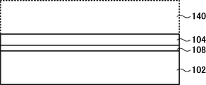
- ベース基板と、
前記ベース基板の上方に位置する第1半導体結晶層と、
前記第1半導体結晶層における一部の領域の上方に位置する第2半導体結晶層と、
前記第2半導体結晶層が上方に位置しない前記第1半導体結晶層の領域の一部をチャネルとし、第1ソースおよび第1ドレインを有する第1MISFETと、
前記第2半導体結晶層の一部をチャネルとし、第2ソースおよび第2ドレインを有する第2MISFETと、を有し、
前記第1MISFETが、第1チャネル型のMISFETであり、前記第2MISFETが、前記第1チャネル型とは相違する第2チャネル型のMISFETであり、
前記第1ソースおよび前記第1ドレインが、前記第1半導体結晶層を構成する原子とニッケル原子との化合物、前記第1半導体結晶層を構成する原子とコバルト原子との化合物、または、前記第1半導体結晶層を構成する原子とニッケル原子とコバルト原子との化合物からなり、
前記第2ソースおよび前記第2ドレインが、前記第2半導体結晶層を構成する原子とニッケル原子との化合物、前記第2半導体結晶層を構成する原子とコバルト原子との化合物、または、前記第2半導体結晶層を構成する原子とニッケル原子とコバルト原子との化合物からなる
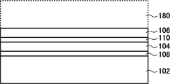
半導体デバイス。 - 前記ベース基板と前記第1半導体結晶層との間に位置し、前記ベース基板と前記第1半導体結晶層とを電気的に分離する第1分離層と、
前記第1半導体結晶層と前記第2半導体結晶層との間に位置し、前記第1半導体結晶層と前記第2半導体結晶層とを電気的に分離する第2分離層と、をさらに有する
請求項1に記載の半導体デバイス。 - 前記第1半導体結晶層と前記第2半導体結晶層との間に位置し、前記第1半導体結晶層と前記第2半導体結晶層とを電気的に分離する第2分離層をさらに有し、
前記ベース基板と前記第1半導体結晶層とが接合面で接し、
前記接合面の近傍における前記ベース基板の領域に、p型またはn型の伝導型を示す不純物原子を含有し、
前記接合面の近傍における前記第1半導体結晶層の領域に、前記ベース基板に含有された不純物原子が示す伝導型とは異なる伝導型を示す不純物原子を含有する
請求項1に記載の半導体デバイス。 - 前記ベース基板と前記第1分離層とが接し、
前記ベース基板の前記第1分離層と接する領域が導電性であり、
前記ベース基板の前記第1分離層と接する領域に印加した電圧が、前記第1MISFETへのバックゲート電圧として作用する
請求項2に記載の半導体デバイス。 - 前記第1半導体結晶層と前記第2分離層とが接し、
前記第1半導体結晶層の前記第2分離層と接する領域が導電性であり、
前記第1半導体結晶層の前記第2分離層と接する領域に印加した電圧が、前記第2MISFETへのバックゲート電圧として作用する
請求項2に記載の半導体デバイス。 - 前記第1半導体結晶層がIV族半導体結晶からなり、前記第1MISFETがPチャネル型MISFETであり、
前記第2半導体結晶層がIII-V族化合物半導体結晶からなり、前記第2MISFETがNチャネル型MISFETである
請求項1に記載の半導体デバイス。 - 前記第1半導体結晶層がIII-V族化合物半導体結晶からなり、前記第1MISFETがNチャネル型MISFETであり、
前記第2半導体結晶層がIV族半導体結晶からなり、前記第2MISFETがPチャネル型MISFETである
請求項1に記載の半導体デバイス。 - 請求項1に記載の半導体デバイスに用いる半導体基板であって、
前記ベース基板と、前記第1半導体結晶層と、前記第2半導体結晶層と、を有し、
前記第1半導体結晶層が、前記ベース基板の上方に位置し、
前記第2半導体結晶層が、前記第1半導体結晶層の一部または全部の上方に位置する
半導体基板。 - 前記ベース基板と前記第1半導体結晶層との間に位置し、前記ベース基板と前記第1半導体結晶層とを電気的に分離する第1分離層と、
前記第1半導体結晶層と前記第2半導体結晶層との間に位置し、前記第1半導体結晶層と前記第2半導体結晶層とを電気的に分離する第2分離層と、をさらに有する
請求項8に記載の半導体基板。 - 前記第1分離層が、非晶質絶縁体からなる
請求項9に記載の半導体基板。 - 前記第1分離層が、前記第1半導体結晶層を構成する半導体結晶の禁制帯幅より大きな禁制帯幅を有する半導体結晶からなる
請求項9に記載の半導体基板。 - 前記第1半導体結晶層と前記第2半導体結晶層との間に位置し、前記第1半導体結晶層と前記第2半導体結晶層とを電気的に分離する第2分離層をさらに有し、
前記ベース基板と前記第1半導体結晶層とが接合面で接し、
前記接合面の近傍における前記ベース基板の領域に、p型またはn型の伝導型を示す不純物原子を含有し、
前記接合面の近傍における前記第1半導体結晶層の領域に、前記ベース基板に含有された不純物原子が示す伝導型とは異なる伝導型を示す不純物原子を含有する
請求項8に記載の半導体基板。 - 前記第2分離層が、非晶質絶縁体からなる
請求項9に記載の半導体基板。 - 前記第2分離層が、前記第2半導体結晶層を構成する半導体結晶の禁制帯幅より大きな禁制帯幅を有する半導体結晶からなる
請求項9に記載の半導体基板。 - 前記第2半導体結晶層を複数有し、
複数の前記第2半導体結晶層のそれぞれが、前記ベース基板の上面と平行な面内で規則的に配列されている
請求項8に記載の半導体基板。 - 請求項8に記載の半導体基板を製造する方法であって、
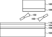
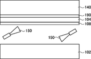
前記ベース基板の上方に前記第1半導体結晶層を形成する第1半導体結晶層形成ステップと、
前記第1半導体結晶層における一部の領域の上方に前記第2半導体結晶層を形成する第2半導体結晶層形成ステップと、を有し、
前記第2半導体結晶層形成ステップが、
半導体結晶層形成基板上に前記第2半導体結晶層をエピタキシャル成長法により形成するエピタキシャル成長ステップと、
前記第1半導体結晶層の上、前記第2半導体結晶層の上、または、前記第1半導体結晶層および前記第2半導体結晶層の両方の上に、前記第1半導体結晶層と前記第2半導体結晶層とを電気的に分離する第2分離層を形成するステップと、
前記第1半導体結晶層上の前記第2分離層と前記第2半導体結晶層とが接合するように、前記第2半導体結晶層上の前記第2分離層と前記第1半導体結晶層とが接合するように、または、前記第1半導体結晶層上の前記第2分離層と前記第2半導体結晶層上の前記第2分離層とが接合するように、前記第1半導体結晶層を有する前記ベース基板と、前記半導体結晶層形成基板とを貼り合わせる貼り合わせステップと、
を有する半導体基板の製造方法。 - 前記第1半導体結晶層形成ステップが、
半導体結晶層形成基板上に前記第1半導体結晶層をエピタキシャル成長法により形成するエピタキシャル成長ステップと、
前記ベース基板の上、前記第1半導体結晶層の上、または、前記ベース基板および前記第1半導体結晶層の両方の上に、前記ベース基板と前記第1半導体結晶層とを電気的に分離する第1分離層を形成するステップと、
前記ベース基板上の前記第1分離層と前記第1半導体結晶層とが接合するように、前記第1半導体結晶層上の前記第1分離層と前記ベース基板とが接合するように、または、前記ベース基板上の前記第1分離層と前記第1半導体結晶層上の前記第1分離層とが接合するように、前記ベース基板と、前記半導体結晶層形成基板とを貼り合わせる貼り合わせステップと、
を有する請求項16に記載の半導体基板の製造方法。 - 前記第1半導体結晶層がSiGeからなり、前記第2半導体結晶層がIII-V族化合物半導体結晶からなり、
前記第1半導体結晶層形成ステップの前に、絶縁体からなる第1分離層を前記ベース基板の上に形成するステップを有し、
前記第1半導体結晶層形成ステップが、
前記第1分離層の上に、前記第1半導体結晶層の出発材料となるSiGe層を形成するステップと、
前記SiGe層を酸化雰囲気中で加熱し、表面を酸化することで前記SiGe層中のGe原子の濃度を高めるステップと、
を有する請求項16に記載の半導体基板の製造方法。 - 前記第1半導体結晶層がIV族半導体結晶からなり、前記第2半導体結晶層がIII-V族化合物半導体結晶からなり、
IV族半導体結晶からなる半導体層材料基板の表面に、絶縁体からなる第1分離層を形成するステップと、
前記第1分離層を通して、陽イオンを前記半導体層材料基板の分離予定深さに注入するステップと、
前記第1分離層の表面と前記ベース基板の表面とが接合されるように、前記半導体層材料基板と前記ベース基板とを貼り合わせるステップと、
前記半導体層材料基板および前記ベース基板を加熱し、前記分離予定深さに注入した前記陽イオンと、前記半導体層材料基板を構成するIV族原子とを反応させることで、前記分離予定深さに位置する前記IV族半導体結晶を変性するステップと、
前記半導体層材料基板と前記ベース基板とを分離することで、前記変性するステップで変性させた前記IV族半導体結晶の変性部位より前記ベース基板側に位置する前記IV族半導体結晶を、前記半導体層材料基板から剥離するステップと、
を有する請求項16に記載の半導体基板の製造方法。 - 前記第1半導体結晶層形成ステップの前に、前記ベース基板の上に前記第1半導体結晶層を構成する半導体結晶の禁制帯幅より大きな禁制帯幅を有する半導体結晶からなる第1分離層をエピタキシャル成長法により形成するステップを有し、
前記第1半導体結晶層形成ステップが、前記第1分離層の上に前記第1半導体結晶層をエピタキシャル成長法により形成するステップである
請求項16に記載の半導体基板の製造方法。 - 前記第1半導体結晶層形成ステップが、前記ベース基板の上に前記第1半導体結晶層をエピタキシャル成長法により形成するステップである
請求項16に記載の半導体基板の製造方法。 - 前記ベース基板の表面近傍に、p型またはn型の伝導型を示す不純物原子を含有し、
前記第1半導体結晶層をエピタキシャル成長法により形成するステップにおいて、前記ベース基板に含有された不純物原子が示す伝導型とは異なる伝導型を示す不純物原子で第1半導体結晶層をドープする
請求項21に記載の半導体基板の製造方法。 - 請求項14に記載の半導体基板を製造する方法であって、
半導体結晶層形成基板の上に前記第2半導体結晶層をエピタキシャル成長法により形成する第2半導体結晶層形成ステップと、
前記第2半導体結晶層の上に、前記第2半導体結晶層を構成する半導体結晶の禁制帯幅より大きな禁制帯幅を有する半導体結晶からなる第2分離層をエピタキシャル成長法により形成する第2分離層形成ステップと、
前記第2分離層の上に前記第1半導体結晶層をエピタキシャル成長法により形成する第1半導体結晶層形成ステップと、
前記ベース基板の上、前記第1半導体結晶層の上、または、前記ベース基板および前記第1半導体結晶層の両方の上に、前記ベース基板と前記第1半導体結晶層とを電気的に分離する第1分離層を形成するステップと、
前記ベース基板上の前記第1分離層と前記第1半導体結晶層とが接合するように、前記第1半導体結晶層上の前記第1分離層と前記ベース基板とが接合するように、または、前記ベース基板上の前記第1分離層と前記第1半導体結晶層上の前記第1分離層とが接合するように、前記ベース基板と、前記半導体結晶層形成基板とを貼り合わせる貼り合わせステップと、
を有する半導体基板の製造方法。 - 前記半導体結晶層形成基板の上に半導体結晶層を形成する前に、前記半導体結晶層形成基板の表面に、結晶性犠牲層をエピタキシャル成長法により形成するステップと、
前記ベース基板と前記半導体結晶層形成基板とを貼り合わせた後に、前記結晶性犠牲層を除去することにより、前記半導体結晶層形成基板上にエピタキシャル成長法により形成された半導体結晶層と前記半導体結晶層形成基板とを分離するステップと、
をさらに有する請求項16に記載の半導体基板の製造方法。 - 前記第2半導体結晶層をエピタキシャル成長させた後に前記第2半導体結晶層を規則的な配列にパターニングするステップ、または前記第2半導体結晶層を予め規則的な配列に選択的にエピタキシャル成長させるステップ、のいずれかのステップを有する
請求項16に記載の半導体基板の製造方法。 - 請求項16に記載の半導体基板の製造方法を用いて、前記第1半導体結晶層および前記第2半導体結晶層を有する半導体基板を製造するステップと、
前記第1半導体結晶層および前記第2半導体結晶層のそれぞれの上にゲート絶縁層を介してゲート電極を形成するステップと、
前記第1半導体結晶層のソース電極形成領域上、前記第1半導体結晶層のドレイン電極形成領域上、前記第2半導体結晶層のソース電極形成領域上、および前記第2半導体結晶層のドレイン電極形成領域上に、ニッケル膜、コバルト膜およびニッケル-コバルト合金膜からなる群から選ばれた金属膜を形成するステップと、
前記金属膜を加熱して、前記第1半導体結晶層に、前記第1半導体結晶層を構成する原子とニッケル原子との化合物、前記第1半導体結晶層を構成する原子とコバルト原子との化合物、または、前記第1半導体結晶層を構成する原子とニッケル原子とコバルト原子との化合物からなる第1ソースおよび第1ドレインを形成し、前記第2半導体結晶層に、前記第2半導体結晶層を構成する原子とニッケル原子との化合物、前記第2半導体結晶層を構成する原子とコバルト原子との化合物、または、前記第2半導体結晶層を構成する原子とニッケル原子とコバルト原子との化合物からなる第2ソースおよび第2ドレインを形成するステップと、
未反応の前記金属膜を除去するステップと、
を有する半導体デバイスの製造方法。
Priority Applications (3)
| Application Number | Priority Date | Filing Date | Title |
|---|---|---|---|
| KR1020137031864A KR20140033070A (ko) | 2011-06-10 | 2012-06-08 | 반도체 디바이스, 반도체 기판, 반도체 기판의 제조 방법 및 반도체 디바이스의 제조 방법 |
| CN201280024791.0A CN103563068B (zh) | 2011-06-10 | 2012-06-08 | 半导体器件、半导体基板、半导体基板的制造方法及半导体器件的制造方法 |
| US14/099,427 US20140091393A1 (en) | 2011-06-10 | 2013-12-06 | Semiconductor device, semiconductor wafer, method for producing semiconductor wafer, and method for producing semiconductor device |
Applications Claiming Priority (2)
| Application Number | Priority Date | Filing Date | Title |
|---|---|---|---|
| JP2011130727 | 2011-06-10 | ||
| JP2011-130727 | 2011-06-10 |
Related Child Applications (1)
| Application Number | Title | Priority Date | Filing Date |
|---|---|---|---|
| US14/099,427 Continuation-In-Part US20140091393A1 (en) | 2011-06-10 | 2013-12-06 | Semiconductor device, semiconductor wafer, method for producing semiconductor wafer, and method for producing semiconductor device |
Publications (1)
| Publication Number | Publication Date |
|---|---|
| WO2012169209A1 true WO2012169209A1 (ja) | 2012-12-13 |
Family
ID=47295792
Family Applications (1)
| Application Number | Title | Priority Date | Filing Date |
|---|---|---|---|
| PCT/JP2012/003769 WO2012169209A1 (ja) | 2011-06-10 | 2012-06-08 | 半導体デバイス、半導体基板、半導体基板の製造方法および半導体デバイスの製造方法 |
Country Status (6)
| Country | Link |
|---|---|
| US (1) | US20140091393A1 (ja) |
| JP (1) | JP2013016789A (ja) |
| KR (1) | KR20140033070A (ja) |
| CN (1) | CN103563068B (ja) |
| TW (1) | TW201308602A (ja) |
| WO (1) | WO2012169209A1 (ja) |
Families Citing this family (4)
| Publication number | Priority date | Publication date | Assignee | Title |
|---|---|---|---|---|
| EP4044257A1 (en) | 2014-06-24 | 2022-08-17 | INTEL Corporation | Techniques for forming ge/sige-channel and iii-v-channel transistors on the same die |
| KR102034175B1 (ko) | 2017-05-30 | 2019-10-18 | 한국과학기술연구원 | 수평 배열된 반도체 채널을 가지는 반도체 소자 및 이의 제조 방법 |
| CN107946390A (zh) * | 2017-12-04 | 2018-04-20 | 孙健春 | 一种具有换电网的太阳能电池及制作方法 |
| DE102019125461A1 (de) * | 2018-09-28 | 2020-04-02 | Taiwan Semiconductor Manufacturing Co., Ltd. | Halbleiterstruktur, vorrichtung und verfahren |
Citations (7)
| Publication number | Priority date | Publication date | Assignee | Title |
|---|---|---|---|---|
| JPS59198750A (ja) * | 1983-04-25 | 1984-11-10 | Seiko Epson Corp | 半導体装置 |
| JPS63311768A (ja) * | 1987-06-13 | 1988-12-20 | Fujitsu Ltd | 相補型半導体装置の製造方法 |
| JPH0384960A (ja) * | 1989-08-28 | 1991-04-10 | Nec Corp | 半導体装置 |
| JPH03109740A (ja) * | 1989-09-25 | 1991-05-09 | Hitachi Ltd | 半導体装置 |
| JP2001093987A (ja) * | 1999-07-29 | 2001-04-06 | Stmicroelectronics Inc | Si基板上のGaAs/Geの新規なCMOS回路 |
| JP2006100403A (ja) * | 2004-09-28 | 2006-04-13 | Fujitsu Ltd | 電界効果型トランジスタおよびその製造方法 |
| JP2007103897A (ja) * | 2005-09-09 | 2007-04-19 | Fujitsu Ltd | 電界効果トランジスタおよびその製造方法 |
Family Cites Families (18)
| Publication number | Priority date | Publication date | Assignee | Title |
|---|---|---|---|---|
| JP2608351B2 (ja) * | 1990-08-03 | 1997-05-07 | キヤノン株式会社 | 半導体部材及び半導体部材の製造方法 |
| JPH06275786A (ja) * | 1993-03-23 | 1994-09-30 | Sony Corp | 相補形化合物半導体装置及びその作製方法 |
| JP3376078B2 (ja) * | 1994-03-18 | 2003-02-10 | 富士通株式会社 | 高電子移動度トランジスタ |
| JP3368449B2 (ja) * | 1994-12-28 | 2003-01-20 | 富士通株式会社 | 半導体装置及びその製造方法 |
| JP3512701B2 (ja) * | 2000-03-10 | 2004-03-31 | 株式会社東芝 | 半導体装置及びその製造方法 |
| US20050275018A1 (en) * | 2004-06-10 | 2005-12-15 | Suresh Venkatesan | Semiconductor device with multiple semiconductor layers |
| US7125785B2 (en) * | 2004-06-14 | 2006-10-24 | International Business Machines Corporation | Mixed orientation and mixed material semiconductor-on-insulator wafer |
| JP4617820B2 (ja) * | 2004-10-20 | 2011-01-26 | 信越半導体株式会社 | 半導体ウェーハの製造方法 |
| US7282425B2 (en) * | 2005-01-31 | 2007-10-16 | International Business Machines Corporation | Structure and method of integrating compound and elemental semiconductors for high-performance CMOS |
| US7342287B2 (en) * | 2005-07-19 | 2008-03-11 | International Business Machines Corporation | Power gating schemes in SOI circuits in hybrid SOI-epitaxial CMOS structures |
| US7696574B2 (en) * | 2005-10-26 | 2010-04-13 | International Business Machines Corporation | Semiconductor substrate with multiple crystallographic orientations |
| FR2911721B1 (fr) * | 2007-01-19 | 2009-05-01 | St Microelectronics Crolles 2 | Dispositif a mosfet sur soi |
| JP5469851B2 (ja) * | 2007-11-27 | 2014-04-16 | 株式会社半導体エネルギー研究所 | 半導体装置の作製方法 |
| US8211786B2 (en) * | 2008-02-28 | 2012-07-03 | International Business Machines Corporation | CMOS structure including non-planar hybrid orientation substrate with planar gate electrodes and method for fabrication |
| US8120110B2 (en) * | 2008-08-08 | 2012-02-21 | International Business Machines Corporation | Semiconductor structure including a high performance FET and a high voltage FET on a SOI substrate |
| JP5478199B2 (ja) * | 2008-11-13 | 2014-04-23 | 株式会社半導体エネルギー研究所 | 半導体装置の作製方法 |
| JP2011014806A (ja) * | 2009-07-06 | 2011-01-20 | Hitachi Ltd | 半導体装置及び半導体装置の製造方法 |
| KR20120049899A (ko) * | 2009-09-04 | 2012-05-17 | 스미또모 가가꾸 가부시키가이샤 | 반도체 기판, 전계 효과 트랜지스터, 집적 회로 및 반도체 기판의 제조 방법 |
-
2012
- 2012-06-08 CN CN201280024791.0A patent/CN103563068B/zh not_active Expired - Fee Related
- 2012-06-08 KR KR1020137031864A patent/KR20140033070A/ko not_active Application Discontinuation
- 2012-06-08 WO PCT/JP2012/003769 patent/WO2012169209A1/ja active Application Filing
- 2012-06-08 JP JP2012130652A patent/JP2013016789A/ja active Pending
- 2012-06-11 TW TW101120879A patent/TW201308602A/zh unknown
-
2013
- 2013-12-06 US US14/099,427 patent/US20140091393A1/en not_active Abandoned
Patent Citations (7)
| Publication number | Priority date | Publication date | Assignee | Title |
|---|---|---|---|---|
| JPS59198750A (ja) * | 1983-04-25 | 1984-11-10 | Seiko Epson Corp | 半導体装置 |
| JPS63311768A (ja) * | 1987-06-13 | 1988-12-20 | Fujitsu Ltd | 相補型半導体装置の製造方法 |
| JPH0384960A (ja) * | 1989-08-28 | 1991-04-10 | Nec Corp | 半導体装置 |
| JPH03109740A (ja) * | 1989-09-25 | 1991-05-09 | Hitachi Ltd | 半導体装置 |
| JP2001093987A (ja) * | 1999-07-29 | 2001-04-06 | Stmicroelectronics Inc | Si基板上のGaAs/Geの新規なCMOS回路 |
| JP2006100403A (ja) * | 2004-09-28 | 2006-04-13 | Fujitsu Ltd | 電界効果型トランジスタおよびその製造方法 |
| JP2007103897A (ja) * | 2005-09-09 | 2007-04-19 | Fujitsu Ltd | 電界効果トランジスタおよびその製造方法 |
Also Published As
| Publication number | Publication date |
|---|---|
| CN103563068B (zh) | 2016-03-23 |
| CN103563068A (zh) | 2014-02-05 |
| KR20140033070A (ko) | 2014-03-17 |
| TW201308602A (zh) | 2013-02-16 |
| JP2013016789A (ja) | 2013-01-24 |
| US20140091393A1 (en) | 2014-04-03 |
Similar Documents
| Publication | Publication Date | Title |
|---|---|---|
| TWI550828B (zh) | 半導體裝置、半導體基板、半導體基板之製造方法及半導體裝置之製造方法 | |
| WO2012169212A1 (ja) | 半導体デバイス、半導体基板、半導体基板の製造方法および半導体デバイスの製造方法 | |
| US8653599B1 (en) | Strained SiGe nanowire having (111)-oriented sidewalls | |
| US7795677B2 (en) | Nanowire field-effect transistors | |
| KR101183273B1 (ko) | 집적회로 및 그의 제조방법 | |
| US7534675B2 (en) | Techniques for fabricating nanowire field-effect transistors | |
| JP5678485B2 (ja) | 半導体装置 | |
| KR20020066191A (ko) | Mos 전계 효과 트랜지스터 | |
| KR20170046560A (ko) | 스트레인을 갖는 적층된 나노시트 fet들 및/또는 양자 우물이 적층된 나노시트 | |
| JP2020202391A (ja) | 異なる歪み状態を有するフィン構造を含む半導体構造を作製するための方法及び関連する半導体構造 | |
| JP2004531054A (ja) | 高速cmos電子機器及び高速アナログ回路のための緩和シリコンゲルマニウムプラットフォーム | |
| JP6560117B2 (ja) | 半導体装置の製造方法 | |
| WO2012169209A1 (ja) | 半導体デバイス、半導体基板、半導体基板の製造方法および半導体デバイスの製造方法 | |
| WO2012169214A1 (ja) | 半導体デバイス、半導体基板、半導体基板の製造方法および半導体デバイスの製造方法 | |
| WO2012169210A1 (ja) | 半導体デバイス、半導体基板、半導体基板の製造方法および半導体デバイスの製造方法 | |
| JP2004055943A (ja) | 半導体装置とその製造方法 | |
| WO2010119239A1 (en) | Uniaxial tensile strain in semiconductor devices | |
| JP2014090121A (ja) | 複合基板の製造方法 | |
| JP7444285B2 (ja) | 半導体構造および電界効果トランジスタの作製方法 | |
| CN103187309B (zh) | 结型场效应晶体管及其制造方法 | |
| US20160380001A1 (en) | Selective oxidation for making relaxed silicon germanium on insulator structures | |
| JP2014090122A (ja) | 複合基板の製造方法 |
Legal Events
| Date | Code | Title | Description |
|---|---|---|---|
| WWE | Wipo information: entry into national phase |
Ref document number: 201280024791.0 Country of ref document: CN |
|
| 121 | Ep: the epo has been informed by wipo that ep was designated in this application |
Ref document number: 12797335 Country of ref document: EP Kind code of ref document: A1 |
|
| ENP | Entry into the national phase |
Ref document number: 20137031864 Country of ref document: KR Kind code of ref document: A |
|
| NENP | Non-entry into the national phase |
Ref country code: DE |
|
| 122 | Ep: pct application non-entry in european phase |
Ref document number: 12797335 Country of ref document: EP Kind code of ref document: A1 |