WO2012153370A1 - Iii族窒化物半導体縦型構造ledチップおよびその製造方法 - Google Patents
Iii族窒化物半導体縦型構造ledチップおよびその製造方法 Download PDFInfo
- Publication number
- WO2012153370A1 WO2012153370A1 PCT/JP2011/002657 JP2011002657W WO2012153370A1 WO 2012153370 A1 WO2012153370 A1 WO 2012153370A1 JP 2011002657 W JP2011002657 W JP 2011002657W WO 2012153370 A1 WO2012153370 A1 WO 2012153370A1
- Authority
- WO
- WIPO (PCT)
- Prior art keywords
- light emitting
- emitting structure
- group iii
- iii nitride
- nitride semiconductor
- Prior art date
- Legal status (The legal status is an assumption and is not a legal conclusion. Google has not performed a legal analysis and makes no representation as to the accuracy of the status listed.)
- Ceased
Links
Images






Classifications
-
- H—ELECTRICITY
- H10—SEMICONDUCTOR DEVICES; ELECTRIC SOLID-STATE DEVICES NOT OTHERWISE PROVIDED FOR
- H10H—INORGANIC LIGHT-EMITTING SEMICONDUCTOR DEVICES HAVING POTENTIAL BARRIERS
- H10H20/00—Individual inorganic light-emitting semiconductor devices having potential barriers, e.g. light-emitting diodes [LED]
- H10H20/80—Constructional details
- H10H20/81—Bodies
- H10H20/811—Bodies having quantum effect structures or superlattices, e.g. tunnel junctions
-
- H—ELECTRICITY
- H10—SEMICONDUCTOR DEVICES; ELECTRIC SOLID-STATE DEVICES NOT OTHERWISE PROVIDED FOR
- H10H—INORGANIC LIGHT-EMITTING SEMICONDUCTOR DEVICES HAVING POTENTIAL BARRIERS
- H10H20/00—Individual inorganic light-emitting semiconductor devices having potential barriers, e.g. light-emitting diodes [LED]
- H10H20/01—Manufacture or treatment
- H10H20/011—Manufacture or treatment of bodies, e.g. forming semiconductor layers
- H10H20/018—Bonding of wafers
-
- H—ELECTRICITY
- H10—SEMICONDUCTOR DEVICES; ELECTRIC SOLID-STATE DEVICES NOT OTHERWISE PROVIDED FOR
- H10H—INORGANIC LIGHT-EMITTING SEMICONDUCTOR DEVICES HAVING POTENTIAL BARRIERS
- H10H20/00—Individual inorganic light-emitting semiconductor devices having potential barriers, e.g. light-emitting diodes [LED]
- H10H20/01—Manufacture or treatment
- H10H20/011—Manufacture or treatment of bodies, e.g. forming semiconductor layers
- H10H20/013—Manufacture or treatment of bodies, e.g. forming semiconductor layers having light-emitting regions comprising only Group III-V materials
- H10H20/0133—Manufacture or treatment of bodies, e.g. forming semiconductor layers having light-emitting regions comprising only Group III-V materials with a substrate not being Group III-V materials
- H10H20/01335—Manufacture or treatment of bodies, e.g. forming semiconductor layers having light-emitting regions comprising only Group III-V materials with a substrate not being Group III-V materials the light-emitting regions comprising nitride materials
-
- H—ELECTRICITY
- H10—SEMICONDUCTOR DEVICES; ELECTRIC SOLID-STATE DEVICES NOT OTHERWISE PROVIDED FOR
- H10H—INORGANIC LIGHT-EMITTING SEMICONDUCTOR DEVICES HAVING POTENTIAL BARRIERS
- H10H20/00—Individual inorganic light-emitting semiconductor devices having potential barriers, e.g. light-emitting diodes [LED]
- H10H20/01—Manufacture or treatment
- H10H20/011—Manufacture or treatment of bodies, e.g. forming semiconductor layers
- H10H20/013—Manufacture or treatment of bodies, e.g. forming semiconductor layers having light-emitting regions comprising only Group III-V materials
- H10H20/0137—Manufacture or treatment of bodies, e.g. forming semiconductor layers having light-emitting regions comprising only Group III-V materials the light-emitting regions comprising nitride materials
-
- H—ELECTRICITY
- H10—SEMICONDUCTOR DEVICES; ELECTRIC SOLID-STATE DEVICES NOT OTHERWISE PROVIDED FOR
- H10H—INORGANIC LIGHT-EMITTING SEMICONDUCTOR DEVICES HAVING POTENTIAL BARRIERS
- H10H20/00—Individual inorganic light-emitting semiconductor devices having potential barriers, e.g. light-emitting diodes [LED]
- H10H20/80—Constructional details
- H10H20/81—Bodies
- H10H20/822—Materials of the light-emitting regions
- H10H20/824—Materials of the light-emitting regions comprising only Group III-V materials, e.g. GaP
-
- H—ELECTRICITY
- H10—SEMICONDUCTOR DEVICES; ELECTRIC SOLID-STATE DEVICES NOT OTHERWISE PROVIDED FOR
- H10H—INORGANIC LIGHT-EMITTING SEMICONDUCTOR DEVICES HAVING POTENTIAL BARRIERS
- H10H20/00—Individual inorganic light-emitting semiconductor devices having potential barriers, e.g. light-emitting diodes [LED]
- H10H20/80—Constructional details
- H10H20/81—Bodies
- H10H20/822—Materials of the light-emitting regions
- H10H20/824—Materials of the light-emitting regions comprising only Group III-V materials, e.g. GaP
- H10H20/825—Materials of the light-emitting regions comprising only Group III-V materials, e.g. GaP containing nitrogen, e.g. GaN
-
- H—ELECTRICITY
- H10—SEMICONDUCTOR DEVICES; ELECTRIC SOLID-STATE DEVICES NOT OTHERWISE PROVIDED FOR
- H10H—INORGANIC LIGHT-EMITTING SEMICONDUCTOR DEVICES HAVING POTENTIAL BARRIERS
- H10H20/00—Individual inorganic light-emitting semiconductor devices having potential barriers, e.g. light-emitting diodes [LED]
- H10H20/80—Constructional details
- H10H20/83—Electrodes
- H10H20/831—Electrodes characterised by their shape
Definitions
- the present invention relates to a vertical structure LED chip in which group III nitride semiconductor layers are stacked and a method for manufacturing the same.
- III-V semiconductors composed of compounds of Group III elements and Group V elements are widely used in devices such as light emitting diodes (LEDs).
- Group III nitride semiconductors using Al, Ga, In, etc. as group III elements and N as group V elements have a high melting point, a high nitrogen dissociation pressure, are difficult to grow bulk single crystals, are large in diameter and inexpensive. Because there is no conductive single crystal substrate, it is generally formed by growing on a sapphire substrate.
- the sapphire substrate is insulative and no current flows, conventionally, an n-type group III nitride semiconductor layer, an active layer (light-emitting layer), and a p-type group III nitride that are sequentially grown on the sapphire substrate.
- the n-type group III nitride semiconductor layer is exposed by removing a part of the light emitting structure laminate composed of the oxide semiconductor layer, and the exposed n-type group III nitride semiconductor layer and p-type group III nitride are exposed. It has been usual to employ a lateral structure in which an n-type electrode and a p-type electrode are respectively disposed on a semiconductor layer and a current flows laterally.
- a buffer layer made of a specific element other than a group III element (eg, Al, Ga, etc.) on a sapphire substrate a light emitting structure laminate is formed, and this light emitting structure laminate is made conductive.
- the buffer layer is selectively dissolved by chemical etching, and the sapphire substrate is peeled off (lifted off), and the support body and the light emitting structure laminate are sandwiched between a pair of electrodes, thereby forming a vertical structure.
- a technique for obtaining the LED chip has been studied (see Patent Document 1).
- the buffer layer here is a buffer layer for epitaxial growth of the light emitting structure laminate, and also serves as a lift-off layer for peeling the light emitting structure laminate from the sapphire substrate.
- a general chemical lift-off method for peeling an epitaxial layer from a sapphire substrate by etching a lift-off layer made of a metal other than Group III or a metal nitride There is a photochemical lift-off method in which etching is performed while irradiating light such as ultraviolet light during the etching and activating the lift-off layer.
- etching is performed while irradiating light such as ultraviolet light during the etching and activating the lift-off layer.
- the lift-off layer to be etched has a thickness of about several nanometers to several tens of nanometers, and it is not easy to supply the etching solution to the gap between the substrate having an area of several inches and the epitaxial layer. could take several days to complete.
- the inventors of the present invention performed groove processing to the sapphire substrate in a grid pattern by dry etching the light-emitting structure laminate formed of a group III nitride semiconductor formed on the sapphire substrate, and the light-emitting structure laminate is divided into a plurality of independent structures.
- the primary separation of the light emitting structure was performed.
- a substrate-shaped conductive support body integrally supporting these light emitting structures was formed, and then the sapphire substrate was peeled off by a chemical lift-off method.
- the individual light emitting structures after the lift-off are still integrally supported by the support body.
- it has been found that cracks are introduced into the lifted-off individual light emitting structures at a considerable ratio. The crack seems to enter when the light emitting structure supported by the support body is released from the bond with the sapphire substrate by lift-off.
- Such cracks may be in the process of research and development, and have not been published in the patent literature or academic literature, but are important to be solved for mass production of group III nitride semiconductor LED chips with vertical structures It is a problem.
- the present invention provides a high-quality group III nitride semiconductor vertical structure LED chip that suppresses cracks generated in the light emitting structure, and a method for more efficiently manufacturing the LED chip. With the goal.
- the gist of the present invention is as follows. (1) A first conductivity type group III nitride semiconductor layer, a light emitting layer, and a second conductivity type group III nitride semiconductor layer different from the first conductivity type are formed on a growth substrate via a lift-off layer.
- a first step of sequentially laminating to form a light emitting structure laminate A second step of forming a plurality of independent light emitting structure parts by removing a part of the light emitting structure laminate so that a part of the growth substrate is exposed; A third step of forming a conductive support body having a lower electrode and integrally supporting the plurality of light emitting structure portions; A fourth step of peeling the growth substrate from the plurality of light emitting structures by removing the lift-off layer using a chemical lift-off method; A fifth step of separating the conductive support bodies between the light emitting structure sections into a plurality of LED chips each having the light emitting structure sections supported by the conductive support bodies.
- a first through hole penetrating at least until the lift-off layer is exposed is formed in the central region of the light emitting structure, and an etching solution is supplied from the first through hole in the fourth step.
- R / L 0 is 0.1, where R is the radius of curvature of the corner of the light emitting structure, and L 0 is the length of one side of the square shape when the light emitting structure is not rounded.
- the first through hole penetrating at least until the lift-off layer is exposed is formed in the central region of the light emitting structure portion, and the etching solution is supplied from the first through hole. It has become possible to more efficiently manufacture a high-quality group III nitride semiconductor vertical structure LED chip with suppressed cracks.
- FIG. 1 is a schematic top view of a group III nitride semiconductor vertical structure LED chip 100 according to an embodiment of the present invention.
- FIG. 1 A) to (D) are photographs of an LED chip before singulation, viewed from above, showing the progress of etching in the process of the manufacturing method according to one embodiment of the present invention. It is a photograph which shows the crack which arose in the corner of the light emission structure part of a LED chip after completion of the etching of FIG.
- FIG. 1 In the manufacturing method concerning other embodiment of this invention, it is a schematic diagram of the light emission structure part for demonstrating the case where the shape of the cross section of a light emission structure part is made into the shape which has a round corner. Is a graph showing the relationship between the R / L 0 and cracking incidence in Embodiment.
- FIG. 10 is a schematic top view of a wafer (a state shown in FIG. 9E) on which a plurality of light emitting structure portions before being singulated are formed.
- A) is a photograph showing cracks generated in the light emitting structure of the LED chip by the manufacturing method of FIG. 9, and (B) is generated in the light emitting structure of the LED chip by the manufacturing method according to the third comparative example. It is a photograph showing a crack.
- the vertical LED chip 300 concerning a 2nd comparative example it is a model top view of the wafer in which the several light emission structure part before dividing into pieces was formed.
- A) is a model top view of the wafer in which the several light emission structure part before dividing into pieces in the manufacturing method of the vertical LED chip 400 concerning a 3rd comparative example was formed
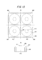
- B) is It is a schematic side view of one LED chip 400 separated into pieces along the broken line of (A).
- (A) is a schematic top view of a wafer on which a plurality of light emitting structures before being singulated is formed in the method for manufacturing a vertical LED chip 500 according to the fourth comparative example
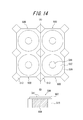
- (B) is It is a model side view of one LED chip 500 separated into pieces along the broken line of (A).
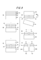
- a manufacturing method of a group III nitride semiconductor vertical structure LED chip (hereinafter simply referred to as “vertical LED chip”) 100 is performed on a growth substrate 101.
- a first conductive group III nitride semiconductor layer 103, a light emitting layer 104, and a second conductive group III nitride semiconductor layer 105 different from the first conductive type are sequentially stacked via a lift-off layer 102.
- the first step of forming the light emitting structure laminate 106 (FIG. 1A) and removing a part of the light emitting structure laminate 106 so that a part of the growth substrate 101 is exposed, for example, in an island shape.
- a second step (FIG.
- the lift-off layer 102 is exposed in the central region of the light emitting structure 107 (in FIG. 1, for growth)
- an etching solution is supplied from the first through hole 108, and the lift-off layer 102 is moved from the central portion to the outer peripheral portion. Select for Characterized by etching.
- the through hole of the light emitting structure 107 is penetrated through the conductive support 109 in a portion located in the central region of the light emitting structure 107 of the conductive support 109.
- a second through hole 110 communicating with 108 is provided.
- a step of forming the upper electrode 111 on the peeling surface side of the light emitting structure 107 can be provided after the fourth step (peeling step).
- the present inventors supply an etching solution from the first through-hole 108 and selectively etch the lift-off layer 102 from the central portion toward the outer peripheral portion, thereby sufficiently cracking the light emitting structure portion 107. It was found that it can be suppressed. Moreover, according to this peeling, the time required for etching can be shortened, and the vertical LED chip can be manufactured more efficiently.
- FIG. 9 schematically shows a flow of a manufacturing method of the vertical LED chip 200 according to the first comparative example.
- a first conductivity type group III nitride semiconductor layer 203, a light emitting layer 204, and a second conductivity type III different from the first conductivity type are formed on a growth substrate 201 via a lift-off layer 202.
- the second step (FIG.
- FIG. 9B for forming a plurality of independent light emitting structure portions 207 by removing the portion, and a conductive support that serves as a lower electrode and supports the plurality of light emitting structure portions 207 integrally.
- a third step of forming the body 209 (FIG. 9C), and a fourth step of removing the growth substrate 201 from the plurality of light emitting structure portions 207 by removing the lift-off layer 202 using a chemical lift-off method. (Fig. 9 (D)) and upper electrode 11 is formed on the peeled surface side of the light emitting structure portion 107 (FIG. 9E), and the conductive support body 209 is separated between the light emitting structure portions 207 by cutting or the like.
- a fifth step (FIG.
- FIG. 10 is a schematic top view of a wafer (a state shown in FIG. 9E) on which a plurality of light emitting structure portions before being singulated is formed, and singulation is performed along a broken line.
- FIG. 11 (A) shows the situation in which cracks were introduced when lift-off was actually performed according to this comparative example, as observed from above with an optical microscope.
- One side of the light emitting structure 207 is 1000 ⁇ m. It can be seen that an X-shaped crack band extending from the vicinity of the corner to the center is generated. (In Comparative Example 1 described later, the crack generation rate was 95.5%.)
- the crack generation rate was 95.5%.
- FIG. 12 is a schematic top view of a wafer on which a plurality of light emitting structure portions before being singulated are formed in the method for manufacturing the vertical LED chip 300 according to the second comparative example.
- This method is the same as the first comparative example except that the cross-sectional shape of the light emitting structure portion 307 is circular in the step of forming a plurality of independent light emitting structure portions 307. That is, there is no through hole in the central region of the light emitting structure portion 307, and no through hole serving as an etching supply port is provided in a portion of the support body 309 located between the light emitting structure portions 307. Therefore, in the fourth step, etching proceeds from the outer peripheral portion of the lift-off layer (not shown).
- reference numeral 311 denotes an upper electrode. Moreover, it divides into pieces along a broken line.
- FIG. 13A is a schematic top view of a wafer on which a plurality of light emitting structure portions 407 before being singulated are formed in the method for manufacturing a vertical LED chip 400 according to the third comparative example.
- (B) is a schematic side view of one LED chip 400 divided into pieces along the broken line of (A).
- This method is the same as that of the second comparative example except that a through groove 412 along the cutting line is provided in a portion of the support body 409 located between the light emitting structure portions 407. That is, the cross-sectional shape of the light emitting structure 407 is circular, and there is no through hole in the central region.
- etching liquid can be supplied from the penetration groove
- reference numeral 411 denotes an upper electrode.
- FIG. 11B is an observation of the situation in which cracks are introduced when the lift-off is actually performed according to this comparative example from the upper surface with an optical microscope. A dot-like crack is generated at the center of the light emitting structure.
- this method since etching proceeds from the outer peripheral portion of each element, the time required for peeling is shorter than that of the first and second comparative examples, but the time required for peeling is further reduced.
- FIG. 14A is a schematic top view of a wafer on which a plurality of light emitting structure portions 507 before being singulated are formed in the method for manufacturing a vertical LED chip 500 according to the fourth comparative example, ) Is a schematic side view of one LED chip 500 singulated along the broken line of (A).
- This method is the same as that of the second comparative example, except that a through hole 513 is provided in a portion of the support body 509 located between the light emitting structure portions (intersection portion of the cutting line). That is, the cross-sectional shape of the light emitting structure 507 is circular, and there is no through hole in the central region.
- reference numeral 511 denotes an upper electrode.
- the mode of cracks generated in each light emitting structure portion 507 after lift-off was the same as in the second comparative example. Also, in this method, since the etching proceeds from the outer peripheral portion of each element, the time required for peeling is shorter than that of the first and second comparative examples, but the time required for peeling is further reduced.
- the present inventors diligently studied the form of occurrence of point-like cracks generated in the second to fourth comparative examples.
- the etching solution is supplied from the outer peripheral side of the light emitting structure portion
- the lift-off layer is etched from the outer peripheral portion toward the central portion.
- local stress is generated at the boundary region between the dissolved front part where the growth substrate and the light emitting structure are bonded via the lift-off layer and the part where they are separated from each other.
- cracks were found to occur.
- the lift-off layer etching still remains in the central portion, so stress concentrates in the central portion and cracks occur.
- the final stage of completion of etching is the central portion of the light emitting structure.
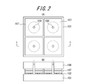
- FIG. 2A is a schematic top view of the wafer in the course of lift-off in the course of the manufacturing method according to one embodiment of the present invention (top view excluding the conductive support 109), and FIG. It is II sectional drawing of the state of a figure (A).
- FIG. 4 is an optical micrograph showing the actual etching progress of Example 1 described later. In this way, the etching solution is supplied from the first through hole 108, and the lift-off layer 102 is selectively etched from the central portion toward the outer peripheral portion.
- the melting front portion proceeds concentrically to the outer peripheral portion, it is possible to avoid stress concentration in the central region of the light emitting structure portion 107, and as a result, point-like in the central region of the light emitting structure portion 107. It is possible to suppress the occurrence of cracks. Furthermore, since etching is not performed from the side surface of the lift-off layer, it is possible to suppress the occurrence of X-type cracks that extend greatly from the corner to the center. In addition, similar etching can be started almost simultaneously in each light emitting structure on the wafer. In addition, the time required for etching could be shortened. As a result, it became possible to manufacture the vertical LED chip more efficiently.
- the etching spreads from the central portion of the lift-off layer 102, it is sufficient that the light emitting structure portions have a function of separating the light emitting structure portions. Can be narrowed, the light emitting area can be increased, and cracks can be suppressed with little loss of the effective area per wafer.
- the effect differs depending on the chip size, as an example, when the dimension of the light emitting structure is 1000 ⁇ m square, the separation groove width of the comparative example was 200 to 250 ⁇ m for securing the etching solution path, but in this method, it can be 80 ⁇ m. .
- the required area per chip was 1.44 to 1.56 mm 2 in the former, but in this embodiment, it may be 1.17 mm 2 , which is an increase of 23 to 33%. That is, the yield per wafer can be increased by the effects of both crack suppression and effective area increase.
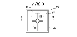
- FIG. 3 is a schematic top view of the group III nitride semiconductor vertical structure LED chip 100.
- the group III nitride semiconductor vertical structure LED chip 100 includes a conductive support 109A having a lower electrode, a second conductive type group III nitride semiconductor layer 105 provided on the conductive support 109A, a second conductive type.
- a light emitting layer 104 provided on the group III nitride semiconductor layer 105 and a first conductivity type group III nitride semiconductor layer 103 having a conductivity type different from the second conductivity type provided on the light emitting layer 104 are provided.
- a light emitting structure 107 having an upper electrode 111 provided on the light emitting structure 107, and a through-hole 108 penetrating the light emitting structure 107 and the support 109 ⁇ / b> A in the central region of the light emitting structure 107. 110.
- Reference numeral 111A denotes a pad electrode.
- the growth substrate 101 is preferably a sapphire substrate or an AlN template substrate in which an AlN film is formed on a sapphire substrate. What is necessary is just to select suitably according to the kind of lift-off layer to form, the composition of Al, Ga, In of the light emitting structure laminated body which consists of a group III nitride semiconductor, the quality of a LED chip, cost, etc.
- the lift-off layer 102 is preferable because a metal other than Group III such as CrN and a metal nitride buffer layer can be dissolved by chemical selective etching. It is preferable to form the film by sputtering, vacuum deposition, ion plating, or MOCVD.
- the light emitting structure laminate 106 may be configured such that the first conductivity type is n-type and the second conductivity type is p-type, or vice versa.
- the first conductive group III nitride semiconductor layer 103, the light emitting layer 104, and the second conductive group III nitride semiconductor layer 105 can be epitaxially grown on the lift-off layer 102 by MOCVD.
- the first through hole 108 may be formed before the fourth step, but is preferably performed simultaneously with the second step. A step of forming a through hole may be separately provided before and after the second step.
- the first through hole is formed through the second through hole in the third step, or a method of using a portion not grown in the first step as a through hole.
- the method of forming can also be considered, these are because man-hours increase and there exists a possibility that productivity may worsen.
- the present invention it is preferable to provide the first through hole 108 at the center of the circumscribed circle of the light emitting structure portion in order to make etching progress highly evenly, but the present invention is not limited to this.
- the “central region” in the present specification is within the region of 0.4 L from the center of the circumscribed circle with respect to the radius (length L) of the circumscribed circle of the light emitting structure, and more preferably within the region of 0.2 L.
- the first through hole 108 may be provided in the central region. Further, when the aspect ratio of the light emitting structure is large (for example, 2 times or more), a plurality of inscribed circles are set, and one or more through holes are formed with the center group of these inscribed circles as a “central region”. It may be provided.
- the cross-sectional shape of the through hole is not particularly limited, and can be, for example, a circle or a shape similar to the shape of the light emitting structure.
- the diameter is preferably 20 ⁇ m or more. If the thickness is less than 20 ⁇ m, when the through-hole 108 is formed by dry etching, a portion that does not reach the lift-off layer may occur in the wafer surface, and the etching of the lift-off layer may not proceed. From the viewpoint of sufficiently obtaining the effect of shortening the etching time, the diameter is more preferably 50 ⁇ m or more. Moreover, even if the through hole is too large, the area loss of the light emitting structure is increased, which is not preferable. From the viewpoint of sufficiently securing the area of the light emitting structure portion, the diameter is preferably 50% or less, and more preferably 30% or less, with respect to the side length L2 of the light emitting structure portion.
- the cross-sectional shape of the light emitting structure 107 is not particularly limited.
- the shape of the light emitting structure can be square in the second step.
- the shape of the cross section of the light emitting structure is preferably a shape having a round corner, and considering the ease of cutting, it is a quadrangular shape having a round corner. More preferred.
- the shape of the light emitting structure is a square as in the embodiment of FIG. 4, the occurrence of X-type cracks extending greatly from the corner to the center can be avoided. As shown in FIG. 5, it was found that very small cracks still occur at the corners. Then, by making the corner round, the stress applied to the light emitting structure 107 when the light emitting structure 107 is moved away from the growth substrate 101 and transferred to the support body 109 at the end of etching is dispersed. It has been found that the generation of such minute cracks can be sufficiently suppressed and a higher quality LED chip can be obtained.
- Having roundness can also be expressed as adding R or chamfering, and the shape is preferably a smooth arc shape, but is not limited to this, and there are a plurality of shaving surfaces that form some curved surface at the corner. It may be in shape.
- the roundness may be very small.
- a large light emitting area can be secured, and cracks can be avoided with a small loss of effective area per wafer.
- the area that decreases by rounding the corners is preferably 10% or less, more preferably 5% or less. can do.
- R / L 0 is R / L 0, where R is the radius of curvature of the corner of the light emitting structure, and L 0 is the length of one side of the square shape when the light emitting structure is not rounded. It is preferable to be within the range of 0.1 to 0.5. If it is less than 0.1, there is a possibility that minute cracks generated at the corner cannot be sufficiently suppressed, and if it exceeds 0.5, the area of the light emitting structure cannot be sufficiently secured.
- the radius of an arc inscribed in two sides intersecting at the corner of the light emitting structure before rounding is referred to as a curvature radius R.
- a plurality of light emitting structure portions 107 and a support body 109 are connected to each of the plurality of light emitting structure portions 107 with an ohmic electrode layer and a connection layer in contact with the support body 109. It is preferable to form via. More preferably, a reflective layer is further formed between the ohmic electrode layer and the connection layer, or the ohmic electrode layer also functions as the reflective layer. For the formation of these layers, dry film forming methods such as vacuum deposition, ion plating, and sputtering can be used.
- the ohmic electrode layer can be formed of a metal having a large work function, for example, a noble metal such as Pd, Pt, Rh, Au, Ag, or Co, Ni. Further, since the reflection layer has a high reflectance such as Rh, it can also be used as the ohmic electrode layer. However, when the light emitting region is from green to blue, an Ag or Al layer is used, and in the ultraviolet region, Rh or Ru is used. More preferably, a layer or the like is used. Further, although the connection layer depends on the method of forming the support body 109, Au, Au—Sn, solder, or the like can be used when the support body 109 is bonded by a bonding method, for example, thermocompression bonding.
- a bonding method for example, thermocompression bonding.
- a conductive silicon substrate, a CuW alloy substrate, a Mo substrate, etc., in which the second through holes 110 are formed in advance are suitable in terms of thermal expansion coefficient and thermal conductivity.
- the through hole positions are aligned and joined.
- the support body 109 can also be formed by wet or dry plating.
- Cu or Au Cu, Ni, Au or the like can be used as the connection layer.
- the first through hole 108 and the second through hole 110 are protected by a resist or the like so as not to be blocked by the connection layer or the plating layer.
- the fourth step is preferably performed by the aforementioned general chemical lift-off method or photochemical lift-off method.
- usable etchants include ceric ammonium nitrate solution and ferricyanium potassium solution when the lift-off layer is CrN, and hydrochloric acid, nitric acid, and organic acids when the lift-off layer is ScN.
- the surface of the light emitting structure 107 exposed in the fourth step is preferably cleaned by wet cleaning.
- a predetermined amount is removed by dry etching and / or wet etching, and an n-type ohmic electrode and a bonding pad electrode are formed by a lift-off method using a resist as a mask.
- Al, Cr, Ti, Ni, Pt, Au, etc. are used as electrode materials, and Pt, Au, etc. are formed as a cover layer on ohmic electrodes and bonding pads to reduce wiring resistance and adhesion of wire bonds.
- a protective film such as SiO 2 or SiN may be provided on the side surface and the surface of the light emitting structure 107. After the lift-off, a protective film may be applied to the through hole.
- the light emitting structure 107 is cut using, for example, a blade dicer or a laser dicer.
- the light emitting structure 107 is generally closer to the inside than the planar outer periphery of the conductive support 109a, but is usually about 10 to 30 ⁇ m.
- Example 1 First, the etching state of the lift-off layer via the through hole in the central portion of the light emitting structure will be described.
- a metal Cr film is formed on a sapphire substrate (0001) substrate by an 18 nm sputtering method, and then subjected to nitriding treatment in an ammonia gas atmosphere in an MOCVD apparatus.
- a blue LED structure layer 10 ⁇ m having an InGaN-based light emitting layer was grown.
- separation grooves were processed to the growth substrate by dry etching.
- the pitch between elements was 1280 ⁇ m. In this case, the corner of the light emitting structure is not intentionally chamfered.
- the light-emitting structure part was subjected to a penetration process with a diameter of 100 ⁇ m.
- a Cu layer was formed to a thickness of 1 ⁇ m by sputtering to form a connection layer for plating.
- a support portion having a thickness of 100 ⁇ m was formed by electroplating.
- a pillar made of a thick film resist was formed in the through hole to prevent the through hole from being blocked during plating. At this time, Cu was not plated at the position of the thick film resist on the through hole, and the through hole penetrating from the light emitting structure to the support body was formed by removing the resist.
- FIG. 4 shows the progress of etching, and is observed with an optical microscope from the transparent sapphire substrate side. Since the lift-off layer has a metallic gray color, it looks black in the picture. 4A shows a state before etching, and as shown in FIG. 4B, it can be seen that the etching progresses uniformly from the concentric circular central portion toward the outside (transparent by dissolution of the lift-off layer). ). In FIG. 4C, the lift-off layer is slightly left at the four corners, but finally the peeling is completed as shown in FIG.
- FIG. 4 shows that in this experimental example, the macro-like X-shaped crack as shown in FIG. 11A does not occur. Further, no dot-like macro cracks were observed from the central part to the entire area. However, when observed in detail, it was found that microcracks having a length of 10 ⁇ m or less may be introduced in the vicinity of the corner as shown in FIG. The reason is considered to be that stress concentrates locally on the portion where the lift-off layer slightly remains in the corner portion as seen in FIG.
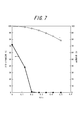
- the experiment was performed using the radius R of the circle inscribed in the orthogonal side as a parameter.
- the sample preparation method is the same as that shown in Experimental Example 1.
- the diameter of the through hole provided in the center of the light emitting structure was 50 ⁇ m.
- Samples with L 0 of 1200 ⁇ m and R of 156, 240, 330, 417, 505, and 600 ⁇ m were prepared.
- the area ratios after chamfering to the square area before chamfering are 98.5, 96.6, 93.5, 89.6, 84.8, and 78.5%, respectively.
- the horizontal axis is the ratio of R with respect to L 0
- the left vertical axis is the incidence of microcracks.
- the right horizontal axis indicates a ratio with respect to the area of the light emitting structure portion when the square portion has no R at the corner portion.
- the range of R / L 0 necessary for suppressing the occurrence of microcracks is 0.1 or more, more preferably 0.2 or more, and the upper limit is 0.5.
- the generation of cracks can be significantly suppressed even when the loss of the light emitting area due to R is 3.4%.
- Example 3 Next, the relationship between the diameter of the through hole for supplying the etching solution and the etching rate of the lift-off layer was examined.
- the sample preparation method is the same as that shown in Experimental Example 1, except that the diameter of the through hole in the central portion of the light emitting structure and the support portion is in the range of 10 ⁇ m to 400 ⁇ m and is etched when immersed in an etching solution for 1 hour. It was evaluated by the amount (diameter of the circle of the melted front part generated by etching).
- FIG. 8 shows the result. As the diameter of the through hole is increased, the etching diameter is increased. However, when the diameter of the through hole is 200 ⁇ m or more, the amount of etching increases gradually.
- the etching solution is supplied only from the central portion, this relationship is unchanged regardless of the planar dimensions of the light emitting structure portion.
- the diameter of the through hole is 10 ⁇ m, etching was possible, but when the light-emitting structure was subjected to through processing by dry etching, the lift-off layer might not be reached in some cases, and the lift-off layer could not be etched. Part occurred. In the case of 20 ⁇ m or more, such a problem did not occur. Therefore, the dimension of the through hole is preferably 20 ⁇ m or more.
- the right vertical axis in FIG. 9 shows the area loss rate of the light emitting structure with respect to the diameter of the through hole when L 0 is 1200 ⁇ m. If L 0 changes, this loss rate changes. Therefore, the diameter of the through hole can be appropriately determined in consideration of the etching rate and the like.
- an n-type group III nitride semiconductor layer GaN layer, thickness: 7 ⁇ m
- a light emitting layer InGaN-based MQW layer, thickness: 0) .1 ⁇ m
- a p-type group III nitride semiconductor layer GaN layer, thickness: 0.2 ⁇ m
- a plurality of independent light emitting structure portions were formed in an island shape so as to be a square having rounded corners.
- the width W of the light emitting structure is 1200 ⁇ m, and the arrangement of the individual elements is within the grid of the grid.
- the pitch between the elements is 1280 ⁇ m.
- the length L 0 of one side of the square before rounding the corner is 1200 ⁇ m, the radius of curvature R of the corner is 330 ⁇ m, and R / L 0 is 0.275.
- a through hole having a diameter of 50 ⁇ m was formed at the center of the independent light emitting structure.
- An ohmic electrode layer (Ag, thickness: 0.1 ⁇ m) and a connection layer (Ti / Cu, thickness: 1.5 ⁇ m) are formed on each light emitting structure (excluding the through hole), and the through hole is formed.
- the holes were plugged with thick film resist.
- Cu (thickness: 80 ⁇ m) was formed by the first plating, and further Cu (thickness: 80 ⁇ m) was formed by the second plating to form a support portion.
- the plating was electroplating using a copper sulfate electrolyte, the temperature of the solution was in the range of 25 to 30 ° C., and the deposition rate was 35 ⁇ m / hr.
- Cu was not plated at the position of the thick film resist on the through hole, and the through hole penetrating from the light emitting structure part to the support part was formed by removing the resist.
- the sapphire substrate was peeled off using a chemical lift-off method.
- the light emitting structure after lift-off was examined for the occurrence of macro and micro cracks using an optical microscope.
- the number of investigations was 3860, and there were no occurrences of macro and micro cracks.
- the time until completion of etching was 2 hours.
- FIG. 10 A sample as shown in FIG. 10 was prepared in the same manner as in the example except that the shape of the light emitting structure was a square of L 0 of 1000 ⁇ m, a through hole was not provided in the central region, and the element pitch was 1250 ⁇ m.
- the light emitting structure after the lift-off was observed with an optical microscope, X-shaped cracks extending greatly from the corner to the center occurred in 1824 out of the 1910 surveyed items, and the occurrence rate was 95.5%. .
- the time until completion of etching was 32 hours.
- FIG. 12 A sample as shown in FIG. 12 was prepared in the same manner as in the example except that the shape of the light emitting structure was a circle having a diameter of 1000 ⁇ m, a through hole was not provided in the central region, and the pitch between elements was 1250 ⁇ m.
- the shape of the light emitting structure was a circle having a diameter of 1000 ⁇ m, a through hole was not provided in the central region, and the pitch between elements was 1250 ⁇ m.
- the shape of the light emitting structure was a circle having a diameter of 1000 ⁇ m, a through hole was not provided in the central region, and the pitch between elements was 1250 ⁇ m.
- the shape of the light emitting structure was a circle having a diameter of 1000 ⁇ m
- a through hole was not provided in the central region
- the pitch between elements was 1250 ⁇ m.
- Comparative Example 3 and Comparative Example 4 In the manufacturing process of Comparative Example 2, as shown in FIG. 13 (Comparative Example 3) or FIG. 14 (Comparative Example 4) in the same manner as Comparative Example 2 except that through grooves or through holes are formed in the support body by the following steps. Sample was prepared.
- An ohmic electrode layer (NiO and Ag) is formed on the p layer of the individual light emitting structure, and then a photoresist is embedded in the separation groove, and the p-ohmic electrode layer of the individual light emitting structure is opened to provide a support body.
- a connection layer (Ni / Au / Cu) for connection to was formed.
- pillars were formed using a thick film resist. The formation position was set on the side of the square surrounding the light emitting structure as shown in FIG. 13A or the intersection of the sides as shown in FIG. The connection layer at the pillar formation position was removed in advance by etching.
- Cu was electroplated with 80 ⁇ m using a copper sulfate-based electrolytic solution to form a support body.
- the liquid temperature was in the range of 25-30 ° C., and the film formation rate was 25 ⁇ m / hr.
- the resist embedded in the pillar portion and the separation groove was removed by chemical cleaning, and grooves and holes penetrating up and down the support body were formed.
- the through-groove shown in FIG. 13A was formed on four sides with a width of 70 ⁇ m and a length of 900 ⁇ m.
- the through-hole shown in FIG. 14A was a quadrangular prism, and the side length was 410 ⁇ m.
- Comparative Example 3 When the light emitting structure after the lift-off was observed with an optical microscope, in Comparative Example 3, among the 1900 surveyed, 38 X-shaped cracks that greatly extended from the corner to the center were generated (occurrence rate was 2. 045), but there were 1045 samples in which dot-like cracks occurred in the central region of the light emitting structure, and the occurrence rate was 55.0%. The time until completion of etching was 3.5 hours. In Comparative Example 4, among the 2038 surveyed items, 108 were X-shaped cracks that greatly extended from the corner to the center (incidence: 5.3%). There were 978 samples in which dot-like cracks occurred in the central region, and the occurrence rate was 48.0%. The time until completion of etching was 4.5 hours.
- the first through hole penetrating at least until the lift-off layer is exposed is formed in the central region of the light emitting structure portion, and the etching solution is supplied from the first through hole. It has become possible to more efficiently manufacture a high-quality group III nitride semiconductor vertical structure LED chip with suppressed cracks.
- Group III Nitride Semiconductor Vertical Structure LED Chip 101 Growth Substrate 102 Lift-off Layer 103 First Conductive Group III Nitride Semiconductor Layer 104 Light Emitting Layer 105 Second Conductive Group III Nitride Semiconductor Layer 106 Light Emitting Structure Laminate 107 light emitting structure 108 first through hole 109 conductive support body 109A having lower electrode conductive support body 109A after cutting 110 second through hole 111 upper electrode 111A pad electrode
Landscapes
- Led Devices (AREA)
Abstract
Description
(1)成長用基板の上にリフトオフ層を介して、第1伝導型のIII族窒化物半導体層、発光層および前記第1伝導型とは異なる第2伝導型のIII族窒化物半導体層を順次積層して発光構造積層体を形成する第1工程と、
前記成長用基板の一部が露出するよう、前記発光構造積層体の一部を除去することで、独立した複数個の発光構造部を形成する第2工程と、
下部電極を有し、前記複数個の発光構造部を一体支持する導電性サポート体を形成する第3工程と、
ケミカルリフトオフ法を用いて、前記リフトオフ層を除去することで、前記成長用基板を前記複数個の発光構造部から剥離する第4工程と、
前記発光構造部間で前記導電性サポート体を分離することにより、各々が導電性サポート体に支持された前記発光構造部を有する複数個のLEDチップに個片化する第5工程と、を有し、
前記第4工程より前に、前記発光構造部の中央領域に、少なくとも前記リフトオフ層が露出するまで貫通する第1貫通孔を形成し、前記第4工程で該第1貫通孔からエッチング液を供給することを特徴とするIII族窒化物半導体縦型構造LEDチップの製造方法。
前記発光構造部の中央領域に、前記発光構造部および前記サポート部を貫通する貫通孔を有することを特徴とするIII族窒化物半導体縦型構造LEDチップ。
図9は、第1の比較例にかかる縦型LEDチップ200の製造方法のフローを模式的に示したものである。この製造方法は、成長用基板201の上にリフトオフ層202を介して、第1伝導型のIII族窒化物半導体層203、発光層204および前記第1伝導型とは異なる第2伝導型のIII族窒化物半導体層205を順次積層して発光構造積層体206を形成する第1工程(図9(A))と、成長用基板201の一部が露出するよう、発光構造積層体206の一部を除去することで、独立した複数個の発光構造部207を形成する第2工程(図9(B))と、下部電極を兼ね、複数個の発光構造部207を一体支持する導電性サポート体209を形成する第3工程(図9(C))と、ケミカルリフトオフ法を用いてリフトオフ層202を除去することで、成長用基板201を複数個の発光構造部207から剥離する第4工程(図9(D))と、上部電極211を発光構造部107の剥離面側に形成する工程と(図9(E))と、発光構造部207間で導電性サポート体209を切断等により分離することにより、各々が切断後の導電性サポート体209Aに支持された発光構造部207を有する複数個のLEDチップ200に個片化する第5工程(図1(E))と、を有する。図10に示すように、発光構造部207の横断面の形状は正方形である。また、発光構造部207の中央領域には貫通孔がなく、サポート体209のうち発光構造部207の間に位置する部分にも特にエッチング供給口となる貫通孔を設けていない。そのため、第4工程ではリフトオフ層202の外周部からエッチングが進行する。図10は、個片化する前の複数の発光構造部が形成されたウェハ(図9(E)の状態)の模式上面図であり、破線に沿って個片化を行う。
図12は、第2の比較例にかかる縦型LEDチップ300の製造方法において、個片化する前の複数の発光構造部が形成されたウェハの模式上面図である。この方法では、独立した複数個の発光構造部307を形成する工程において、発光構造部307の横断面形状を円形にした点以外、第1の比較例と同様である。すなわち、発光構造部307の中央領域には貫通孔がなく、サポート体309のうち発光構造部307の間に位置する部分にも特にエッチング供給口となる貫通孔を設けていない。そのため、第4工程ではリフトオフ層(図示せず)の外周部からエッチングが進行する。図12において、符号311は上部電極である。また、破線に沿って個片化を行う。
図13(A)は、第3の比較例にかかる縦型LEDチップ400の製造方法において、個片化する前の複数の発光構造部407が形成されたウェハの模式上面図であり、図13(B)は、(A)の破線に沿って個片化した1つのLEDチップ400の模式側面図である。この方法では、サポート体409のうち発光構造部407の間に位置する部分に切断ラインに沿った貫通溝412を設けた以外、第2の比較例と同様である。すなわち、発光構造部407の横断面形状は円形であり、その中央領域には貫通孔がない。そして、貫通溝412からエッチング液が供給可能なので、第4工程では、個片化前の各LEDチップの外周部からエッチングが進行する。図13において、符号411は上部電極である。
図14(A)は、第4の比較例にかかる縦型LEDチップ500の製造方法において、個片化する前の複数の発光構造部507が形成されたウェハの模式上面図であり、(B)は、(A)の破線に沿って個片化した1つのLEDチップ500の模式側面図である。この方法では、サポート体509のうち発光構造部の間に位置する部分(切断ラインの交点部分)に貫通孔513を設けた以外、第2の比較例と同様である。すなわち、発光構造部507の横断面形状は円形であり、その中央領域には貫通孔がない。そして、貫通孔513からエッチング液が供給可能なので、第4工程では、個片化前の各LEDチップの外周部からエッチングが進行する。図14において、符号511は上部電極である。
本発明者らは、第2~第4の比較例で生じる点状のクラックの発生形態について鋭意検討を行った。第3、第4の比較例のように、発光構造部の外周側からのエッチング液供給の場合、リフトオフ層は外周部から中央部に向けてエッチングが進行するが、成長用基板と発光構造部がまさに分離している溶解フロント部、すなわちリフトオフ層を介して成長用基板と発光構造部が接着状態である部分と、それらが分離された状態となった部分の境界領域で局所的な応力が加わってクラックが発生することが判明した。リフトオフ層のエッチングが終了する間際は、中央部分にリフトオフ層がまだ残っているため、中央部で応力が集中しクラックが発生する。第2の比較例の場合でも、エッチング終了の最終段階は、発光構造部の中央部分となる。
成長用基板101は、サファイア基板またはサファイア基板上にAlN膜を形成したAlNテンプレート基板を用いるのが好ましい。形成するリフトオフ層の種類やIII族窒化物半導体からなる発光構造積層体のAl、Ga、Inの組成、LEDチップの品質、コストなどにより適宜選択すればよい。
発光構造積層体106の一部の除去には、ドライエッチング法を用いるのが好ましい。これは、III族窒化物半導体層で構成される発光構造積層体106のエッチングの終点を再現性良く制御できるからである。また、隣接する発光構造部107が繋がった状態であると、後工程で再度分離溝加工が必要となるためこの除去は、成長用基板101の一部が露出するまで行うものとする。第1貫通孔108の形成は第4工程よりも前であれば良いが、この第2工程の時に同時に行うことが好ましい。第2工程の前後に貫通孔の形成工程を別途設けても良く、さらに第1工程にて成長させない箇所を貫通孔とする方法や、第3工程にて第2貫通孔を通して第1貫通孔を形成する方法も考えられるが、これらは工数が増えるため生産性が悪くなる恐れがあるためである。
図には示されないが、第3工程は、複数個の発光構造部107とサポート体109とを、複数個の発光構造部107の各々と接するオーミック電極層、およびサポート体109と接する接続層を介して形成するのが好ましい。また、オーミック電極層と接続層との間にさらに反射層を形成するか、オーミック電極層が反射層の機能を兼ねることがより好ましい。これらの層形成には、真空蒸着法、イオンプレーティング法、スパッタリング法などの乾式成膜法を用いることができる。
第4工程は、前述の一般的なケミカルリフトオフ法またはフォトケミカルリフトオフ法により行うのが好ましい。使用可能なエッチング液としては、リフトオフ層がCrNの場合、硝酸第二セリウムアンモン溶液やフェリシアンカリウム系の溶液、リフトオフ層がScNの場合、塩酸、硝酸、有機酸などを挙げることができる。
第5工程では、発光構造部107間を例えばブレードダイサーやレーザーダイサーを用いて切断する。発光構造部107に熱や破砕ダメージが入るのを防止するため、一般には発光構造部107は導電性サポート部109aの平面外周よりも内側に寄せるが、通常10から30μm程度である。
初めに、発光構造部の中央部の貫通孔を経由したリフトオフ層のエッチング状況について説明する。サファイア基板(0001)基板上に、金属Crを18nmスパッタリング法により成膜し、ついでMOCVD装置内でアンモニアガス雰囲気で窒化処理を行った後、形成されたCrNバッファ層(リフトオフ層を兼ねる)上にInGaN系発光層を有する青色LED構造層10μmを成長した。次に、1200μm角の正方形に発光構造部を形成するため、ドライエッチングにより成長基板まで分離溝加工を行った。素子間ピッチは1280μmとした。この場合、発光構造部のコーナーは意図的な面取りは行っていない。同時に、発光構造部に直径100μmの貫通加工処理を行った。次に、Cu層をスパッタリング法により1μm成膜してめっき用の接続層を形成した。さらに、電気めっき法により100μm厚みのサポート部を形成した。なお、貫通孔に厚膜レジストによるピラーを形成し、めっき中の貫通孔の閉塞を防いだ。このとき、貫通孔上の厚膜レジストの位置にはCuはめっきされず、レジストを除去することで、発光構造部からサポート体まで貫通する貫通孔を形成した。
そこで、リフトオフ層のエッチングの終了間際の部分での応力集中を回避するため、溶解終了部分に応力が分散できるようにすることを考えた。発光構造部の中央部からエッチング液を供給してリフトオフ層をエッチングする場合、図4に示したように、エッチングは等方的に円が広がるように進行する。図6に示すように発光構造部の平面の4コーナー部の円弧の長さが、応力の分散具合と関連するので、コーナー部の面取り形状とマイクロクラックの発生率を調べた。なお、4コーナーの1箇所でもマイクロクラックが発生した場合には、チップとしては不良となるので、個々のチップ単位で発生の有無で判定した。
次に、エッチング液の供給を行う貫通孔の径と、リフトオフ層のエッチング速度との関係を調べた。試料の作製方法は実験例1に示したものと同様であるが、発光構造部の中央部ならびにサポート部の貫通孔の直径を10μmから400μmの範囲として、エッチング液に1時間浸漬した際のエッチング量(エッチングされて生じた溶解フロント部の円の直径)で評価した。図8はその結果を示したものであるが、貫通孔の直径を大きくするほどエッチング径は大きくなる。しかしながら、貫通孔の直径が200μm以上になるとエッチング量の増加が緩やかになった。なお、中央部からのみのエッチング液の給液であるため、発光構造部の平面寸法によらずこの関係は不変的なものである。また、貫通孔の径が10μmの場合は、エッチングは可能であったが、ドライエッチングで発光構造物に貫通加工を行った際に、リフトオフ層までとどかない場合があり、リフトオフ層をエッチングができない部分が生じた。20μm以上の場合にはそのような問題は生じなかった。したがって、貫通孔の寸法としては、20μm以上が好ましい。なお、図9の右側縦軸はL0が1200μmの際の、貫通孔の直径に対する発光構造部の面積ロス率を示したものである。L0が変わればこのロス率は変化するので、エッチング速度等を加味して適宜貫通孔の直径を決定することができる。
サファイア基板上に、リフトオフ層(CrN層、厚さ:18nm)を形成後、n型III族窒化物半導体層(GaN層、厚さ:7μm)、発光層(InGaN系MQW層、厚さ:0.1μm)、p型III族窒化物半導体層(GaN層、厚さ:0.2μm)を順次積層して発光構造積層体を形成し、その後、サファイア基板の一部が露出するよう、発光構造積層体の一部を除去することで、コーナーに丸みを有する正方形となるよう、島状に独立した複数個の発光構造部を形成した。発光構造部の幅Wは1200μmであり、個々の素子の配置は碁盤の目状の升目内とした。素子間のピッチは1280μmである。コーナーに丸みを付与する前の正方形の一辺の長さL0は1200μm、コーナーの曲率半径Rは330μmであり、R/L0は0.275である。
発光構造部の形状をL0は1000μmの正方形とし、中央領域に貫通孔を設けず、素子間ピッチを1250μmとした以外は、実施例と同様にして図10のような試料を作製した。リフトオフ後の発光構造部を光学顕微鏡によって観察したところ、調査個数1910個のうち1824個に、コーナーから中央部に大きく伸展するX型のクラックが発生し、発生率は95.5%であった。また、エッチング完了までの時間は32時間であった。
発光構造部の形状を直径1000μmの円形とし、中央領域に貫通孔を設けず、素子間ピッチを1250μmとした以外は、実施例と同様にして図12のような試料を作製した。リフトオフ後の発光構造部を光学顕微鏡によって観察したところ、調査個数1890個のうち、コーナーから中央部に大きく伸展するX型のクラックが発生したものは437個(発生率は23.1%)であったが、発光構造部の中央部に点状のクラックが発生した試料が1607個あり、発生率は85.0%であった。また、エッチング完了までの時間は28時間であった。
比較例2の製造工程において、以下の工程によってサポート体に貫通溝または貫通孔を形成した以外は、比較例2と同様にして図13(比較例3)または図14(比較例4)のような試料を作製した。
101 成長用基板
102 リフトオフ層
103 第1伝導型のIII族窒化物半導体層
104 発光層
105 第2伝導型のIII族窒化物半導体層
106 発光構造積層体
107 発光構造部
108 第1貫通孔
109 下部電極を有する導電性サポート体
109A 切断後の導電性サポート体
110 第2貫通孔
111 上部電極
111A パッド電極
Claims (9)
- 成長用基板の上にリフトオフ層を介して、第1伝導型のIII族窒化物半導体層、発光層および前記第1伝導型とは異なる第2伝導型のIII族窒化物半導体層を順次積層して発光構造積層体を形成する第1工程と、
前記成長用基板の一部が露出するよう、前記発光構造積層体の一部を除去することで、独立した複数個の発光構造部を形成する第2工程と、
下部電極を有し、前記複数個の発光構造部を一体支持する導電性サポート体を形成する第3工程と、
ケミカルリフトオフ法を用いて、前記リフトオフ層を除去することで、前記成長用基板を前記複数個の発光構造部から剥離する第4工程と、
前記発光構造部間で前記導電性サポート体を分離することにより、各々が導電性サポート体に支持された前記発光構造部を有する複数個のLEDチップに個片化する第5工程と、を有し、
前記第4工程より前に、前記発光構造部の中央領域に、少なくとも前記リフトオフ層が露出するまで貫通する第1貫通孔を形成し、前記第4工程で該第1貫通孔からエッチング液を供給することを特徴とするIII族窒化物半導体縦型構造LEDチップの製造方法。 - 前記第3工程において、前記導電性サポート体における前記発光構造部の中央領域に位置する部分に、該導電性サポート体を貫通して前記発光構造部の貫通孔と連通する第2貫通孔を設ける請求項1に記載のIII族窒化物半導体縦型構造LEDチップの製造方法。
- 前記第2工程において、前記発光構造部の横断面の形状を、コーナーに丸みを有する形状とする請求項1または2に記載のIII族窒化物半導体縦型構造LEDチップの製造方法。
- 前記第2工程において、前記発光構造部の横断面の形状を、コーナーに丸みを有する4角形状とする請求項3に記載のIII族窒化物半導体縦型構造LEDチップの製造方法。
- 前記発光構造部のコーナーの曲率半径をR、前記発光構造部がコーナーに丸みを有しない場合の前記4角形状の一辺の長さをL0として、R/L0が0.1~0.5の範囲内である請求項4に記載のIII族窒化物半導体縦型構造LEDチップの製造方法。
- 前記第1貫通孔および/または第2貫通孔の直径が、20μm以上である請求項1~5のいずれか1項に記載のIII族窒化物半導体縦型構造LEDチップの製造方法。
- 前記第3工程は、接合法、湿式成膜法、乾式成膜法のいずれかを用いて行われる請求項1~6のいずれか1項に記載のIII族窒化物半導体縦型構造LEDチップの製造方法。
- 請求項1~7のいずれか1項に記載の方法により製造された縦型構造LEDチップであって、前記発光構造部の中央領域に第1貫通孔を有することを特徴とするIII族窒化物半導体縦型構造LEDチップ。
- 下部電極を有する導電性サポート体と、該導電性サポート体上に設けられた第2伝導型III族窒化物半導体層、該第2伝導型III族窒化物半導体層の上に設けられた発光層、および、該発光層の上に設けられた前記第2伝導型とは異なる伝導型の第1伝導型III族窒化物半導体層を有する発光構造部と、該発光構造部上に設けられた上部電極と、を有し、
前記発光構造部の中央領域に、前記発光構造部および前記サポート部を貫通する貫通孔を有することを特徴とするIII族窒化物半導体縦型構造LEDチップ。
Priority Applications (5)
| Application Number | Priority Date | Filing Date | Title |
|---|---|---|---|
| JP2013513828A JP5723442B2 (ja) | 2011-05-12 | 2011-05-12 | Iii族窒化物半導体縦型構造ledチップおよびその製造方法 |
| US14/117,281 US9502603B2 (en) | 2011-05-12 | 2011-05-12 | Vertically structured group III nitride semiconductor LED chip and method for manufacturing the same |
| CN201180072086.3A CN103814447B (zh) | 2011-05-12 | 2011-05-12 | 垂直型第iii族氮化物半导体led芯片及其制造方法 |
| KR1020137032452A KR20140041527A (ko) | 2011-05-12 | 2011-05-12 | Ⅲ족 질화물 반도체 수직형 구조 led 칩 및 그 제조 방법 |
| PCT/JP2011/002657 WO2012153370A1 (ja) | 2011-05-12 | 2011-05-12 | Iii族窒化物半導体縦型構造ledチップおよびその製造方法 |
Applications Claiming Priority (1)
| Application Number | Priority Date | Filing Date | Title |
|---|---|---|---|
| PCT/JP2011/002657 WO2012153370A1 (ja) | 2011-05-12 | 2011-05-12 | Iii族窒化物半導体縦型構造ledチップおよびその製造方法 |
Publications (1)
| Publication Number | Publication Date |
|---|---|
| WO2012153370A1 true WO2012153370A1 (ja) | 2012-11-15 |
Family
ID=47138873
Family Applications (1)
| Application Number | Title | Priority Date | Filing Date |
|---|---|---|---|
| PCT/JP2011/002657 Ceased WO2012153370A1 (ja) | 2011-05-12 | 2011-05-12 | Iii族窒化物半導体縦型構造ledチップおよびその製造方法 |
Country Status (5)
| Country | Link |
|---|---|
| US (1) | US9502603B2 (ja) |
| JP (1) | JP5723442B2 (ja) |
| KR (1) | KR20140041527A (ja) |
| CN (1) | CN103814447B (ja) |
| WO (1) | WO2012153370A1 (ja) |
Cited By (5)
| Publication number | Priority date | Publication date | Assignee | Title |
|---|---|---|---|---|
| JPWO2013046267A1 (ja) * | 2011-09-28 | 2015-03-26 | ビービーエスエイ リミテッドBBSA Limited | 半導体素子およびその製造方法 |
| CN104851945A (zh) * | 2015-04-17 | 2015-08-19 | 西安神光皓瑞光电科技有限公司 | 一种垂直结构led芯片制备方法 |
| CN104900766A (zh) * | 2014-03-07 | 2015-09-09 | 晶能光电(常州)有限公司 | 一种高压led芯片的制备方法 |
| CN105280759A (zh) * | 2014-07-25 | 2016-01-27 | 晶能光电(常州)有限公司 | 一种晶圆级薄膜倒装led芯片的制备方法 |
| WO2022004294A1 (ja) * | 2020-07-03 | 2022-01-06 | 信越半導体株式会社 | 接合型半導体ウェーハの製造方法及び接合型半導体素子の製造方法 |
Families Citing this family (11)
| Publication number | Priority date | Publication date | Assignee | Title |
|---|---|---|---|---|
| EP2912685B1 (en) * | 2012-10-26 | 2020-04-08 | RFHIC Corporation | Semiconductor devices with improved reliability and operating life and methods of manufacturing the same |
| US10551165B2 (en) * | 2015-05-01 | 2020-02-04 | Adarza Biosystems, Inc. | Methods and devices for the high-volume production of silicon chips with uniform anti-reflective coatings |
| KR102410788B1 (ko) | 2015-06-30 | 2022-06-21 | 쑤저우 레킨 세미컨덕터 컴퍼니 리미티드 | 발광 소자 |
| KR102603867B1 (ko) * | 2016-08-01 | 2023-11-21 | 삼성디스플레이 주식회사 | 유기 발광 표시 장치 및 유기 발광 표시 장치의 제조 방법 |
| TWI641128B (zh) * | 2017-07-10 | 2018-11-11 | 英屬開曼群島商錼創科技股份有限公司 | 顯示裝置 |
| TWI632675B (zh) * | 2017-07-10 | 2018-08-11 | 錼創科技股份有限公司 | 顯示面板 |
| JP6431631B1 (ja) * | 2018-02-28 | 2018-11-28 | 株式会社フィルネックス | 半導体素子の製造方法 |
| CN108470720B (zh) * | 2018-03-23 | 2020-07-28 | 广东省半导体产业技术研究院 | 利用湿法腐蚀剥离衬底的方法 |
| US11152533B1 (en) * | 2018-09-21 | 2021-10-19 | Facebook Technologies, Llc | Etchant-accessible carrier substrate for display manufacture |
| JP2024064494A (ja) * | 2022-10-28 | 2024-05-14 | 沖電気工業株式会社 | 半導体素子の製造方法、半導体層支持構造体、および半導体基板 |
| JP2024064422A (ja) * | 2022-10-28 | 2024-05-14 | 沖電気工業株式会社 | 半導体素子の製造方法、半導体層支持構造体、および半導体基板 |
Citations (8)
| Publication number | Priority date | Publication date | Assignee | Title |
|---|---|---|---|---|
| JP2008078275A (ja) * | 2006-09-20 | 2008-04-03 | Tohoku Univ | 化合物半導体素子の製造方法 |
| JP2010093186A (ja) * | 2008-10-10 | 2010-04-22 | Showa Denko Kk | 窒化ガリウム系化合物半導体発光素子の製造方法、窒化ガリウム系化合物半導体素子の積層構造及び窒化ガリウム系化合物半導体発光素子、並びにランプ |
| JP2010147164A (ja) * | 2008-12-17 | 2010-07-01 | Stanley Electric Co Ltd | 半導体素子の製造方法 |
| JP2010147166A (ja) * | 2008-12-17 | 2010-07-01 | Stanley Electric Co Ltd | 半導体素子の製造方法 |
| JP2010287681A (ja) * | 2009-06-10 | 2010-12-24 | Toyoda Gosei Co Ltd | Iii族窒化物半導体発光素子の製造方法 |
| WO2011055462A1 (ja) * | 2009-11-05 | 2011-05-12 | ウェーブスクエア,インコーポレイテッド | Iii族窒化物半導体縦型構造ledチップならびにその製造方法 |
| JP2011096707A (ja) * | 2009-10-27 | 2011-05-12 | Stanley Electric Co Ltd | 半導体素子の製造方法 |
| JP2011096881A (ja) * | 2009-10-30 | 2011-05-12 | Showa Denko Kk | 半導体発光素子、半導体発光素子の製造方法、半導体発光素子を用いた照明装置および電子機器 |
Family Cites Families (26)
| Publication number | Priority date | Publication date | Assignee | Title |
|---|---|---|---|---|
| JPS5116869A (en) | 1974-08-02 | 1976-02-10 | Hitachi Ltd | Handotaisochino seizoho |
| JPH02240975A (ja) | 1989-03-14 | 1990-09-25 | Toshiba Corp | 化合物半導体発光装置及びその製造方法 |
| JPH08293476A (ja) | 1995-04-21 | 1996-11-05 | Hitachi Ltd | 半導体集積回路装置の製造方法および半導体ウエハならびにフォトマスク |
| JP4437337B2 (ja) | 1999-06-08 | 2010-03-24 | 住友精密工業株式会社 | 半導体デバイスの製造方法 |
| JP3893874B2 (ja) | 1999-12-21 | 2007-03-14 | 日亜化学工業株式会社 | 窒化物半導体発光素子の製造方法 |
| JP2002076435A (ja) | 2000-09-05 | 2002-03-15 | Mitsubishi Cable Ind Ltd | 半導体発光素子 |
| US20030189215A1 (en) * | 2002-04-09 | 2003-10-09 | Jong-Lam Lee | Method of fabricating vertical structure leds |
| JP2005252222A (ja) | 2004-02-03 | 2005-09-15 | Matsushita Electric Ind Co Ltd | 半導体発光装置、照明モジュール、照明装置、表示素子、および半導体発光装置の製造方法 |
| US6924210B1 (en) | 2004-03-06 | 2005-08-02 | International Business Machines Corporation | Chip dicing |
| JP2006030329A (ja) | 2004-07-13 | 2006-02-02 | Ricoh Co Ltd | 電子写真感光体およびその製造方法 |
| JP2006086300A (ja) * | 2004-09-15 | 2006-03-30 | Sanken Electric Co Ltd | 保護素子を有する半導体発光装置及びその製造方法 |
| JP2006086469A (ja) | 2004-09-17 | 2006-03-30 | Matsushita Electric Ind Co Ltd | 半導体発光装置、照明モジュール、照明装置及び半導体発光装置の製造方法 |
| US7211500B2 (en) | 2004-09-27 | 2007-05-01 | United Microelectronics Corp. | Pre-process before cutting a wafer and method of cutting a wafer |
| JP2006228855A (ja) | 2005-02-16 | 2006-08-31 | Rohm Co Ltd | 半導体発光素子およびその製法 |
| JP4817673B2 (ja) | 2005-02-25 | 2011-11-16 | 三洋電機株式会社 | 窒化物系半導体素子の作製方法 |
| KR100976268B1 (ko) | 2005-04-04 | 2010-08-18 | 가부시키가이샤 토호쿠 테크노 아치 | GaN 단결정 성장방법, GaN 기판 제작방법, GaN계소자 제조방법 및 GaN계 소자 |
| KR100638732B1 (ko) | 2005-04-15 | 2006-10-30 | 삼성전기주식회사 | 수직구조 질화물 반도체 발광소자의 제조방법 |
| EP1798781B1 (en) | 2005-12-15 | 2009-08-05 | LG Electronics Inc. | LED having vertical structure and method for fabricating the same |
| US7439548B2 (en) * | 2006-08-11 | 2008-10-21 | Bridgelux, Inc | Surface mountable chip |
| JP4765916B2 (ja) * | 2006-12-04 | 2011-09-07 | サンケン電気株式会社 | 半導体発光素子 |
| US7648891B2 (en) | 2006-12-22 | 2010-01-19 | International Business Machines Corporation | Semiconductor chip shape alteration |
| KR20090028931A (ko) | 2007-09-17 | 2009-03-20 | 삼성전기주식회사 | 반도체 발광소자 |
| JP2009099681A (ja) | 2007-10-15 | 2009-05-07 | Shinko Electric Ind Co Ltd | 基板の個片化方法 |
| US8211781B2 (en) * | 2008-11-10 | 2012-07-03 | Stanley Electric Co., Ltd. | Semiconductor manufacturing method |
| JP2011029612A (ja) | 2009-06-24 | 2011-02-10 | Toyoda Gosei Co Ltd | Iii族窒化物半導体発光素子 |
| JP5281545B2 (ja) * | 2009-11-04 | 2013-09-04 | スタンレー電気株式会社 | 半導体発光素子の製造方法 |
-
2011
- 2011-05-12 US US14/117,281 patent/US9502603B2/en active Active
- 2011-05-12 CN CN201180072086.3A patent/CN103814447B/zh active Active
- 2011-05-12 WO PCT/JP2011/002657 patent/WO2012153370A1/ja not_active Ceased
- 2011-05-12 JP JP2013513828A patent/JP5723442B2/ja active Active
- 2011-05-12 KR KR1020137032452A patent/KR20140041527A/ko not_active Abandoned
Patent Citations (8)
| Publication number | Priority date | Publication date | Assignee | Title |
|---|---|---|---|---|
| JP2008078275A (ja) * | 2006-09-20 | 2008-04-03 | Tohoku Univ | 化合物半導体素子の製造方法 |
| JP2010093186A (ja) * | 2008-10-10 | 2010-04-22 | Showa Denko Kk | 窒化ガリウム系化合物半導体発光素子の製造方法、窒化ガリウム系化合物半導体素子の積層構造及び窒化ガリウム系化合物半導体発光素子、並びにランプ |
| JP2010147164A (ja) * | 2008-12-17 | 2010-07-01 | Stanley Electric Co Ltd | 半導体素子の製造方法 |
| JP2010147166A (ja) * | 2008-12-17 | 2010-07-01 | Stanley Electric Co Ltd | 半導体素子の製造方法 |
| JP2010287681A (ja) * | 2009-06-10 | 2010-12-24 | Toyoda Gosei Co Ltd | Iii族窒化物半導体発光素子の製造方法 |
| JP2011096707A (ja) * | 2009-10-27 | 2011-05-12 | Stanley Electric Co Ltd | 半導体素子の製造方法 |
| JP2011096881A (ja) * | 2009-10-30 | 2011-05-12 | Showa Denko Kk | 半導体発光素子、半導体発光素子の製造方法、半導体発光素子を用いた照明装置および電子機器 |
| WO2011055462A1 (ja) * | 2009-11-05 | 2011-05-12 | ウェーブスクエア,インコーポレイテッド | Iii族窒化物半導体縦型構造ledチップならびにその製造方法 |
Cited By (6)
| Publication number | Priority date | Publication date | Assignee | Title |
|---|---|---|---|---|
| JPWO2013046267A1 (ja) * | 2011-09-28 | 2015-03-26 | ビービーエスエイ リミテッドBBSA Limited | 半導体素子およびその製造方法 |
| CN104900766A (zh) * | 2014-03-07 | 2015-09-09 | 晶能光电(常州)有限公司 | 一种高压led芯片的制备方法 |
| CN104900766B (zh) * | 2014-03-07 | 2018-03-27 | 晶能光电(常州)有限公司 | 一种高压led芯片的制备方法 |
| CN105280759A (zh) * | 2014-07-25 | 2016-01-27 | 晶能光电(常州)有限公司 | 一种晶圆级薄膜倒装led芯片的制备方法 |
| CN104851945A (zh) * | 2015-04-17 | 2015-08-19 | 西安神光皓瑞光电科技有限公司 | 一种垂直结构led芯片制备方法 |
| WO2022004294A1 (ja) * | 2020-07-03 | 2022-01-06 | 信越半導体株式会社 | 接合型半導体ウェーハの製造方法及び接合型半導体素子の製造方法 |
Also Published As
| Publication number | Publication date |
|---|---|
| US20140319557A1 (en) | 2014-10-30 |
| CN103814447B (zh) | 2016-04-20 |
| US9502603B2 (en) | 2016-11-22 |
| CN103814447A (zh) | 2014-05-21 |
| KR20140041527A (ko) | 2014-04-04 |
| JP5723442B2 (ja) | 2015-05-27 |
| JPWO2012153370A1 (ja) | 2014-07-28 |
Similar Documents
| Publication | Publication Date | Title |
|---|---|---|
| JP5723442B2 (ja) | Iii族窒化物半導体縦型構造ledチップおよびその製造方法 | |
| JP5690738B2 (ja) | Iii族窒化物半導体縦型構造ledチップの製造方法 | |
| CN101901858B (zh) | 垂直结构半导体器件 | |
| JP5774712B2 (ja) | 半導体素子およびその製造方法 | |
| JP2008521220A (ja) | 機能が向上された厚い超伝導フィルム | |
| JP6059238B2 (ja) | Iii族窒化物半導体素子およびその製造方法 | |
| US8921227B2 (en) | Semiconductor device assembly and semiconductor device and method of manufacturing the same | |
| TW200849673A (en) | LED chip production method | |
| JP5934720B2 (ja) | Iii族窒化物半導体素子およびその製造方法 | |
| JP2009283762A (ja) | 窒化物系化合物半導体ledの製造方法 | |
| JP5723431B2 (ja) | Iii族窒化物半導体縦型構造ledチップ | |
| JP2010161198A (ja) | 半導体発光素子、半導体発光素子用ウェハ、半導体発光素子の製造方法、及び半導体発光素子用ウェハの製造方法 | |
| JP5763858B2 (ja) | Iii族窒化物半導体縦型構造ledチップの製造方法 | |
| JP5936696B2 (ja) | Iii族窒化物半導体素子およびその製造方法 |
Legal Events
| Date | Code | Title | Description |
|---|---|---|---|
| WWE | Wipo information: entry into national phase |
Ref document number: 201180072086.3 Country of ref document: CN |
|
| 121 | Ep: the epo has been informed by wipo that ep was designated in this application |
Ref document number: 11865272 Country of ref document: EP Kind code of ref document: A1 |
|
| ENP | Entry into the national phase |
Ref document number: 2013513828 Country of ref document: JP Kind code of ref document: A |
|
| NENP | Non-entry into the national phase |
Ref country code: DE |
|
| ENP | Entry into the national phase |
Ref document number: 20137032452 Country of ref document: KR Kind code of ref document: A |
|
| WWE | Wipo information: entry into national phase |
Ref document number: 14117281 Country of ref document: US |
|
| 122 | Ep: pct application non-entry in european phase |
Ref document number: 11865272 Country of ref document: EP Kind code of ref document: A1 |