WO2012137445A1 - Procédé de pilotage de dispositif d'imagerie à semi-conducteurs - Google Patents
Procédé de pilotage de dispositif d'imagerie à semi-conducteurs Download PDFInfo
- Publication number
- WO2012137445A1 WO2012137445A1 PCT/JP2012/002150 JP2012002150W WO2012137445A1 WO 2012137445 A1 WO2012137445 A1 WO 2012137445A1 JP 2012002150 W JP2012002150 W JP 2012002150W WO 2012137445 A1 WO2012137445 A1 WO 2012137445A1
- Authority
- WO
- WIPO (PCT)
- Prior art keywords
- row
- reset
- state imaging
- pixel
- imaging device
- Prior art date
Links
- 238000003384 imaging method Methods 0.000 title claims abstract description 84
- 238000000034 method Methods 0.000 title claims abstract description 64
- 238000009825 accumulation Methods 0.000 claims description 12
- 230000008859 change Effects 0.000 abstract description 7
- 239000011159 matrix material Substances 0.000 abstract description 3
- 239000003990 capacitor Substances 0.000 description 31
- 238000010586 diagram Methods 0.000 description 31
- 238000006243 chemical reaction Methods 0.000 description 28
- 206010047571 Visual impairment Diseases 0.000 description 22
- 239000010410 layer Substances 0.000 description 21
- 230000000875 corresponding effect Effects 0.000 description 16
- 239000000758 substrate Substances 0.000 description 14
- 230000003321 amplification Effects 0.000 description 13
- 238000003199 nucleic acid amplification method Methods 0.000 description 13
- 238000005070 sampling Methods 0.000 description 12
- 230000008878 coupling Effects 0.000 description 9
- 238000010168 coupling process Methods 0.000 description 9
- 238000005859 coupling reaction Methods 0.000 description 9
- 230000003071 parasitic effect Effects 0.000 description 9
- 230000000903 blocking effect Effects 0.000 description 6
- 239000000470 constituent Substances 0.000 description 5
- 238000002955 isolation Methods 0.000 description 4
- 239000004065 semiconductor Substances 0.000 description 4
- 230000002596 correlated effect Effects 0.000 description 3
- 230000001681 protective effect Effects 0.000 description 3
- 238000009792 diffusion process Methods 0.000 description 2
- 230000000694 effects Effects 0.000 description 2
- 239000011229 interlayer Substances 0.000 description 2
- 230000031700 light absorption Effects 0.000 description 2
- 229910044991 metal oxide Inorganic materials 0.000 description 2
- 150000004706 metal oxides Chemical class 0.000 description 2
- 230000008569 process Effects 0.000 description 2
- 230000035484 reaction time Effects 0.000 description 2
- 230000009467 reduction Effects 0.000 description 2
- 229910004298 SiO 2 Inorganic materials 0.000 description 1
- XUIMIQQOPSSXEZ-UHFFFAOYSA-N Silicon Chemical compound [Si] XUIMIQQOPSSXEZ-UHFFFAOYSA-N 0.000 description 1
- ATJFFYVFTNAWJD-UHFFFAOYSA-N Tin Chemical compound [Sn] ATJFFYVFTNAWJD-UHFFFAOYSA-N 0.000 description 1
- 239000011358 absorbing material Substances 0.000 description 1
- 230000002457 bidirectional effect Effects 0.000 description 1
- 230000000295 complement effect Effects 0.000 description 1
- 230000007423 decrease Effects 0.000 description 1
- 238000007599 discharging Methods 0.000 description 1
- AMGQUBHHOARCQH-UHFFFAOYSA-N indium;oxotin Chemical compound [In].[Sn]=O AMGQUBHHOARCQH-UHFFFAOYSA-N 0.000 description 1
- 238000002347 injection Methods 0.000 description 1
- 239000007924 injection Substances 0.000 description 1
- 239000000463 material Substances 0.000 description 1
- 230000007246 mechanism Effects 0.000 description 1
- 230000003287 optical effect Effects 0.000 description 1
- 230000002093 peripheral effect Effects 0.000 description 1
- 238000005096 rolling process Methods 0.000 description 1
- 229910052710 silicon Inorganic materials 0.000 description 1
- 239000010703 silicon Substances 0.000 description 1
- 239000007787 solid Substances 0.000 description 1
- 230000009466 transformation Effects 0.000 description 1
- 238000001771 vacuum deposition Methods 0.000 description 1
Images


Classifications
-
- H—ELECTRICITY
- H04—ELECTRIC COMMUNICATION TECHNIQUE
- H04N—PICTORIAL COMMUNICATION, e.g. TELEVISION
- H04N25/00—Circuitry of solid-state image sensors [SSIS]; Control thereof
- H04N25/70—SSIS architectures; Circuits associated therewith
- H04N25/71—Charge-coupled device [CCD] sensors; Charge-transfer registers specially adapted for CCD sensors
- H04N25/75—Circuitry for providing, modifying or processing image signals from the pixel array
-
- H—ELECTRICITY
- H04—ELECTRIC COMMUNICATION TECHNIQUE
- H04N—PICTORIAL COMMUNICATION, e.g. TELEVISION
- H04N25/00—Circuitry of solid-state image sensors [SSIS]; Control thereof
- H04N25/60—Noise processing, e.g. detecting, correcting, reducing or removing noise
- H04N25/62—Detection or reduction of noise due to excess charges produced by the exposure, e.g. smear, blooming, ghost image, crosstalk or leakage between pixels
- H04N25/626—Reduction of noise due to residual charges remaining after image readout, e.g. to remove ghost images or afterimages
-
- H—ELECTRICITY
- H04—ELECTRIC COMMUNICATION TECHNIQUE
- H04N—PICTORIAL COMMUNICATION, e.g. TELEVISION
- H04N25/00—Circuitry of solid-state image sensors [SSIS]; Control thereof
- H04N25/70—SSIS architectures; Circuits associated therewith
- H04N25/71—Charge-coupled device [CCD] sensors; Charge-transfer registers specially adapted for CCD sensors
- H04N25/745—Circuitry for generating timing or clock signals
-
- H—ELECTRICITY
- H04—ELECTRIC COMMUNICATION TECHNIQUE
- H04N—PICTORIAL COMMUNICATION, e.g. TELEVISION
- H04N25/00—Circuitry of solid-state image sensors [SSIS]; Control thereof
- H04N25/70—SSIS architectures; Circuits associated therewith
- H04N25/76—Addressed sensors, e.g. MOS or CMOS sensors
- H04N25/78—Readout circuits for addressed sensors, e.g. output amplifiers or A/D converters
-
- H—ELECTRICITY
- H01—ELECTRIC ELEMENTS
- H01L—SEMICONDUCTOR DEVICES NOT COVERED BY CLASS H10
- H01L27/00—Devices consisting of a plurality of semiconductor or other solid-state components formed in or on a common substrate
- H01L27/14—Devices consisting of a plurality of semiconductor or other solid-state components formed in or on a common substrate including semiconductor components sensitive to infrared radiation, light, electromagnetic radiation of shorter wavelength or corpuscular radiation and specially adapted either for the conversion of the energy of such radiation into electrical energy or for the control of electrical energy by such radiation
- H01L27/144—Devices controlled by radiation
- H01L27/146—Imager structures
- H01L27/14601—Structural or functional details thereof
- H01L27/14609—Pixel-elements with integrated switching, control, storage or amplification elements
Definitions
- the present invention relates to a method for driving a solid-state imaging device that outputs an image as an electrical signal.
- CMOS Complementary Metal Oxide Semiconductor
- MOS Metal Oxide Semiconductor
- CCD image sensor charge-coupled device CCD image sensor
- a conventional solid-state imaging device has a configuration in which pixels having a photoelectric conversion unit (photodiode) and a readout circuit unit are arranged in a two-dimensional array on the outermost surface of a semiconductor substrate. Therefore, the area of the photoelectric conversion unit is reduced by the area of the readout circuit unit on the light incident surface. As a result, the conventional solid-state imaging device has a problem that the aperture ratio decreases.
- Patent Document 1 and Patent Document 2 disclose stacked solid-state imaging devices each including a photoelectric conversion unit having a structure in which a light-absorbing material is stacked on a substrate and a readout circuit formed on the substrate. It has been reported.
- the photoelectric conversion unit of each pixel includes a pixel electrode, a photoelectric conversion film stacked above (light incident side), and a counter electrode formed on the upper surface thereof. including.
- the multilayer solid-state imaging device takes out a charge group generated by incident light as a current signal outside the photoelectric conversion unit via the pixel electrode.
- the stacked solid-state imaging device usually includes a charge blocking layer that conducts signal charges to select a sign of signal charges and blocks charges of opposite signs. The charge blocking layer faces the pixel electrode or is in direct contact with the pixel electrode.
- FIG. 14 schematically shows a circuit of a pixel portion (pixel) of a conventional stacked image sensor using an organic film described in Patent Document 1 as a photoelectric conversion film.
- the signal charge output from the photoelectric conversion unit 101 through the pixel electrode 102 is stored in the charge storage unit 103 formed of a depletion layer capacitance formed on the substrate.
- the charge storage unit 103 is connected to an input gate of a pixel readout transistor (amplification transistor) 104 via a wiring, and a selection transistor 105 that detects a change in voltage associated with a change in the amount of stored charge and selects a readout timing of the pixel.
- amplification transistor amplification transistor
- the drain part of the reset transistor 106 is connected to the charge storage part 103 in order to reset the charge of the charge storage part 103, and the charge storage part voltage is set to the initial state voltage at the time of reset. Is set.
- FIG. 15 schematically shows a stacked solid-state imaging device in which the pixels of FIG. 14 are two-dimensionally arranged, and n rows (n is an integer of 2 or more) of pixels are arranged in the vertical scanning direction. ing.
- the gates of the reset transistors 106 in each row are controlled by one reset control line for each row.
- the gate of the selection transistor 105 is controlled by a selection control line.
- Each row is numbered from 1 to n in the vertical scanning direction, the reset control line of the i-th row (i is an integer not less than 1 and not more than (n ⁇ 1)) is res_ (i), and the selection control line is sel_ (I) and a typical driving method of the multilayer solid-state imaging device at the time of moving image shooting will be described with reference to FIG.
- FIG. 16 is a diagram for explaining a typical driving method by showing a voltage applied to each control line and an output voltage appearing on a vertical signal line 107 in a certain column.
- FIG. 16 only the (i ⁇ 1) th to (i + 1) th rows are shown, but if the same driving is sequentially performed from the first to nth rows, an image signal for one screen can be obtained. Since it can be easily understood by those skilled in the art, it is omitted.
- the driving period (horizontal scanning period) of the i-th row is described as the (i) th scanning period.
- res_ (i ⁇ 1) is turned on, and the charge accumulation unit 103 is reset by the reset transistor 106 (a reset voltage is given to the reset transistor 106 in advance by a voltage source or the like). Thereafter, res_ (i-1) is turned off to complete the reset operation of the (i-1) th row, and the voltage V2 (referred to as a reset signal) output to the vertical signal line 107 is output by a CDS circuit or the like. Sampling is performed (this operation is hereinafter referred to as “reset signal reading”). Thereby, the difference between the sampling voltage V1 and the voltage V2 is obtained as the output voltage of the CDS circuit.
- the output voltage of the CDS circuit obtained in each column is sequentially output to the outside of the solid-state imaging device by the horizontal transfer circuit, and the driving in the (i-1) th scanning period is finished.
- the same driving is performed even after the next (i) scanning period.
- the same driving is repeated from the (1) th scanning period of the next frame.
- the output voltage V1 in the next frame is obtained by adding the voltage corresponding to the light intensity irradiated to each pixel to the output voltage V2 in the previous frame, and thus the voltage (V1-V2) obtained by the CDS circuit. ) Is a true image signal depending only on the light intensity.
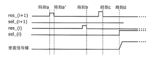
- FIG. 17 is a diagram showing two pixels in the i-th row and the (i + 1) -th row adjacent in the vertical scanning direction, and the configuration of each pixel is the same as that in FIG. However, in FIG. 17, a parasitic capacitance 108 between these pixels is added.
- the parasitic capacitance 108 is generated between the pixel electrodes 102, between the gate wirings of the pixel readout transistor 104, and the like.
- the value of the charge storage unit (storage capacitor) 103 is Ca (this is usually the same value for all pixels), and the value of the parasitic capacitor 108 is Cp.
- Vres (i) the voltage of the storage capacitor 103 (i) after the reset operation of the (i) th row is completed, that is, immediately after res_ (i) is turned off, is Vres (i).
- the voltage of the storage capacitor 103 (i + 1) at this time is set to Vfd1 (i + 1).
- Vres1 (i) is determined by the reset voltage applied to the reset transistor 106 (i), the threshold value of the reset transistor 106 (i), and the gate-drain capacitance (assuming the storage capacitor 103 side is the drain), and is applied to the pixel. It does not depend on the light intensity.
- Vfd1 (i + 1) depends on the light intensity applied to the pixels in the (i + 1) th row.
- ⁇ is a value that depends on the selection transistor 105 and other parasitic capacitances, and does not depend on the amount of light irradiation.
- the voltage of the storage capacitor 103 (i) when the selection transistor 105 (i) is turned on is substantially equal to the sum of Qa and Vres2 (i).
- the voltage value is Vout (i)
- Vout (i) depends on Vfd1 (i + 1), which appears as an afterimage. For example, if the intensity of light irradiated to the (i + 1) th row in the previous frame is high, the value of Vout (i) becomes small depending on it. As an image, a black and white inverted version of the image of the previous frame is superimposed on the current frame. Note that ⁇ is a value due to a parasitic component similar to ⁇ .
- the present invention has been made in view of the above-described prior art, and provides a driving method of a solid-state imaging device that enables high-quality imaging without occurrence of an afterimage phenomenon even when capturing moving images with a sharp change in luminance. With the goal.
- a driving method of a solid-state imaging device includes pixels arranged in a two-dimensional array of m columns in the horizontal scanning direction and n rows in the vertical scanning direction.
- This is a driving method of the solid-state imaging device (n is an integer of 2 or more, m is a natural number), and the reset operation of the pixel in the i-th row (i is an integer of 1 to n-1) is completed.
- the pixel in the (i + 1) th row is being reset, or the elapsed time after the pixel in the (i + 1) th row has finished the reset operation is less than one frame imaging time.
- the potential fluctuation of the output signal due to coupling of the reset operation of the row adjacent to the predetermined row does not occur. Therefore, no afterimage occurs between frames.
- the driving method of the solid-state imaging device includes an accumulation time of j horizontal scanning periods (j is an integer of 1 to (n ⁇ 1)).
- j is an integer of 1 to (n ⁇ 1)
- the driving method of the solid-state imaging device is to read out pixel signals of the (i + 1) -th row (i is an integer of 1 to n-1).
- the operation, the start of the reset operation of the (i + 1) -th row, and the end of the reset operation of the i-th row are sequentially performed.
- the potential fluctuation of the output signal due to the coupling of the reset operation of the adjacent row can be removed by the second reset operation, so that no afterimage is generated between frames.
- the driving method of the solid-state imaging device is to read out pixel signals of the (i + 1) -th row (i is an integer of 1 to n-1).
- the operation, the start of the reset operation of the (i + 1) th row, the end of the reset operation of the (i + 1) th row, the reset signal reading operation of the (i + 1) th row, and the end of the reset operation of the ith row are sequentially performed. It is characterized by performing.
- the potential fluctuation of the output signal due to the coupling of the reset operation of the adjacent row can be removed by the second reset operation, so that no afterimage is generated between frames.
- the driving method of the solid-state imaging device is to read out pixel signals of the (i + 1) -th row (i is an integer of 1 to n-1).
- the operation, the start of the reset operation of the (i + 1) th row, the end of the reset operation of the i row, and the reset signal read operation of the i row are sequentially performed.
- the potential fluctuation of the output signal due to the coupling of the reset operation of the adjacent row can be removed by the second reset operation, so that no afterimage is generated between frames.
- a driving method of a solid-state imaging device is a two-dimensional form of m columns in the horizontal scanning direction and 2k rows or (2k + 1) rows in the vertical scanning direction.
- a + 1) -th pixel signal (a is an integer of 0 to k) Operation, driving of the odd-numbered frame in which the reset operation of the (2a + 1) th row, the reset signal reading operation of the (2a + 1) th row, and the reset operation of the 2a row are sequentially performed, and the pixel signal reading of the (2a + 2) th row And an even-numbered frame driving in which the reset operation of the (2a + 2) th row, the reset signal reading operation of the (2a + 2) th row, and the reset operation of the (2a + 1) th row are sequentially performed.
- a driving method of the imaging apparatus can be provided.
- FIG. 1 is a diagram illustrating each part of the stacked solid-state imaging device according to Embodiment 1 of the present invention.
- FIG. 2 is a cross-sectional view of the solid-state imaging device according to Embodiment 1 of the present invention.
- FIG. 3A is a diagram illustrating a method for driving the solid-state imaging device according to Embodiment 1 of the present invention.
- FIG. 3B is a diagram illustrating a method for driving the solid-state imaging device according to Embodiment 1 of the present invention.
- FIG. 4 is a diagram for explaining the solid-state imaging device according to the second embodiment of the present invention.
- FIG. 5 is a diagram illustrating a method for driving the solid-state imaging device according to the second embodiment of the present invention.
- FIG. 6A is a diagram illustrating a method for driving the solid-state imaging device according to Embodiment 3 of the present invention.
- FIG. 6B is a diagram illustrating a method for driving the solid-state imaging device according to Embodiment 3 of the present invention.
- FIG. 7 is a diagram for explaining the solid-state imaging device according to the fourth embodiment of the present invention.
- FIG. 8 is a diagram illustrating a driving method of the solid-state imaging device according to the fourth embodiment of the present invention.
- FIG. 9 is a diagram illustrating a solid-state imaging device according to Embodiment 5 of the present invention.
- FIG. 10 is a diagram for explaining the solid-state imaging device according to the fifth embodiment of the present invention.
- FIG. 10 is a diagram for explaining the solid-state imaging device according to the fifth embodiment of the present invention.
- FIG. 11 is a diagram for explaining a driving method of the solid-state imaging device according to the fifth embodiment of the present invention.
- FIG. 12 is a diagram illustrating a solid-state imaging device according to Embodiment 6 of the present invention.
- FIG. 13 is a diagram for explaining a driving method of the solid-state imaging device according to the sixth embodiment of the present invention.
- FIG. 14 is a diagram illustrating pixels of a conventional stacked solid-state imaging device.
- FIG. 15 is a diagram illustrating a pixel array of the solid-state imaging device.
- FIG. 16 is a diagram illustrating a method for driving the solid-state imaging device.
- FIG. 17 is a diagram illustrating a pixel portion of the solid-state imaging device.
- Embodiment 1 A method for driving the solid-state imaging device according to Embodiment 1 of the present invention will be described with reference to FIGS. 1 to 3B.
- FIG. 1 is a block diagram showing a configuration of a solid-state imaging device 501 according to Embodiment 1 of the present invention.
- the solid-state imaging device 501 includes a pixel array 502, row signal driving circuits 503a and 503b, a column amplifier circuit 504 arranged for each column, a noise canceller circuit 505 arranged for each column, a horizontal driving circuit 506, And an output stage amplifier 507.
- FIG. 2 is a cross-sectional view of an area corresponding to three pixels of the solid-state imaging device 501.
- the actual pixels are arranged in the pixel array 502, for example, for 10 million pixels.
- the circuit diagram of each pixel is the same as FIG.
- the solid-state imaging device 501 includes a microlens 601, a red color filter 602, a green color filter 603, a blue color filter 604, a protective film 605, a planarization film 606, and an upper electrode 607.
- photoelectric conversion film 608 electron blocking layer 609
- interelectrode insulating film 610 lower electrode 611 (first electrode)
- interwiring insulating film 612 feeding layer 613, wiring layer 614, a substrate 618, a well 619, an STI region (shallow trench isolation region) 620, and an interlayer insulating layer 621.
- the substrate 618 is a semiconductor substrate, for example, a silicon substrate.
- a signal readout circuit for reading out signal charges generated by photoelectric conversion of the photoelectric conversion film 608 to the outside of the pixel as a signal voltage (readout signal), that is, a plurality of transistors (amplification transistor 616, selection transistor, and reset) Transistor 617) is formed.
- the micro lens 601 is formed for each pixel 510 on the outermost surface of the solid-state imaging device 501 in order to efficiently collect incident light.
- the red color filter 602, the green color filter 603, and the blue color filter 604 are formed for capturing a color image. Further, the red color filter 602, the green color filter 603, and the blue color filter 604 are formed immediately below each microlens 601 and in the protective film 605. These optical elements are formed on the planarizing film 606 in order to form a microlens 601 and a color filter group free from unevenness of color collection and color over 10 million pixels.
- the planarizing film 606 is made of SiN, for example.
- the upper electrode 607 is formed under the planarizing film 606 over the entire surface of the pixel array 502.
- the upper electrode 607 transmits visible light.
- the upper electrode 607 is made of ITO (Indium Tin Oxide).
- the photoelectric conversion film 608 converts light into signal charges. Specifically, the photoelectric conversion film 608 is formed under the upper electrode 607 and is composed of organic molecules having high light absorption ability. Moreover, the thickness of the photoelectric conversion film 608 is, for example, 500 nm. Further, the photoelectric conversion film 608 is formed by using a vacuum evaporation method. The organic molecule has a high light absorption ability over the entire visible light having a wavelength of 400 nm to 700 nm.
- the electron blocking layer 609 is formed under the photoelectric conversion film 608 and conducts holes generated by photoelectric conversion of incident light and blocks injection of electrons from the lower electrode 611.
- the electron blocking layer 609 is formed on the interelectrode insulating film 610 and the lower electrode 611 having high flatness.
- the plurality of lower electrodes 611 are arranged in a matrix above the substrate 618.
- the plurality of lower electrodes 611 are electrically isolated from each other.
- the lower electrode 611 is formed between the interelectrode insulating films 610 and collects holes generated in the photoelectric conversion film 608.
- the lower electrode 611 is made of, for example, TiN.
- the lower electrode 611 is formed on the planarized inter-wiring insulating film 612 having a thickness of 100 nm.
- the lower electrodes 611 are separated by an interval of 0.2 ⁇ m.
- An interelectrode insulating film 610 is also embedded in this isolation region.
- a power feeding layer 613 is disposed below the isolation region and below the inter-wiring insulating film 612.
- the power supply layer 613 is made of Cu, for example.
- the power feeding layer 613 is a region between the adjacent lower electrodes 611 and is formed between the lower electrode 611 and the substrate 618.
- a potential independent of the lower electrode 611 can be supplied to the power feeding layer 613.
- a potential for discharging signal charges is supplied to the power supply layer 613 during an exposure operation in which the photoelectric conversion film 608 performs photoelectric conversion and in a read operation in which the signal read circuit generates a read signal.
- a positive voltage is applied. Thereby, it can prevent that a hole mixes into each pixel from an adjacent pixel.
- Such voltage application control is performed, for example, by a control unit (not shown) included in the solid-state imaging device 501.
- a wiring layer 614 is connected to the power feeding layer 613.
- the wiring layer 614 is connected to the FD portion (charge storage portion) 615 and the gate terminal of the amplification transistor 616 of the signal readout circuit.
- the FD portion 615 is electrically connected to the source terminal of the reset transistor 617.
- the source terminal of the reset transistor 617 and the FD unit 615 share a diffusion region.
- These transistors, a selection transistor (not shown) formed in the same pixel, and the FD portion 615 are all formed in the same P-type well 619.
- the well 619 is formed on the substrate 618.
- the signal readout circuit is formed on the substrate 618 and generates a readout signal corresponding to the signal charge by detecting a change in current or voltage generated in each of the plurality of lower electrodes 611.
- the amplification transistor 616 generates a read signal by amplifying a change in current or voltage generated in the lower electrode 611.
- each transistor is electrically isolated by configured STI region 620 in SiO 2.
- the gate terminal of the reset transistor 617 is connected to the reset control line, and the on / off of the reset transistor 617 is controlled by the potential of the reset control line. For example, when the potential of the reset control line is set to a high level and the reset control line is turned on, the reset transistor 617 is turned on, and the potential of the reset control line is set to a low level and the reset control line is turned off. The reset transistor 617 is turned off.
- the gate terminal of the selection transistor is connected to the selection control line, and the on / off of the selection transistor is controlled by the potential of the selection control line. For example, when the potential of the selection control line is set to high level and the selection control line is turned on, the selection transistor is turned on, and when the potential of the selection control line is set to low level and the selection control line is turned off, The selection transistor is turned off.
- the configuration of the pixel array 502 of this embodiment is the same as that in FIG. 16, and n rows (n is an integer of 2 or more) in the vertical scanning direction and m rows (m is a natural number) are arranged in the horizontal direction. Has been.
- FIG. 3A and 3B are diagrams showing a driving method of the solid-state imaging device in the present embodiment. This shows the signals given to each control line in time series. Further, although only the i-th and (i + 1) -th lines are shown, it is easy for those skilled in the art to apply this to the normal vertical scanning operation.
- the reset control line in the i-th row is referred to as res_ (i), and the selection control line is referred to as sel_ (i).
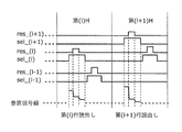
- FIG. 3A will be described.
- res_ (i) is turned on to start the reset operation of the i-th row.
- the voltage of the FD portion 615 (storage capacitor 103 (i + 1)) in the (i + 1) th row at time b is Vfd2 (i + 1), and the FD in the (i + 1) th row at time c.
- the voltage of the unit 615 (storage capacitor 103 (i + 1)) is Vfd3 (i + 1)
- the voltage of the FD unit 615 (storage capacitor 103 (i)) in the (i) th row is as follows.
- Vfd2 (i + 1) is a value immediately after reset during reset operation of the (i + 1) th row, and does not depend on the light irradiation amount. If time b in FIG. 3A is the previous frame of time d, which is the time of reading, no matter what light irradiation state was in the previous frame, an output independent of it will be obtained at time d, The afterimage removal which is the subject of the present invention can be achieved. Actually, if the solid-state imaging device is driven so as to satisfy the driving method shown in FIG. 3A described above (this example is shown in the following embodiment), the afterimage can be removed.
- FIG. 3B shows another driving method.
- res_ (i + 1) is turned off at time a ′, and the reset of the (i + 1) th row is completed.
- res_ (i + 1) is turned off at time c, and reset of the (i + 1) -th row is completed (res_ (i + 1) is turned on before time c).
- the operation at time d is the same as the driving method of FIG. 3A.
- the voltage of the FD unit 615 (storage capacitor 103 (i + 1)) in the (i) th row at time b is Vfd2 (i + 1) ′, and the FD unit 615 (storage capacitor 103 (i + 1) in the (i + 1) th row at time c. ) Is Vfd3 (i + 1) ′, the output voltage at time d is considered in the same way as in FIG. 3A.
- Vfd2 (i + 1) ′ depends on the light irradiation amount. However, if the time difference between the time a ′ and the time b is shortened, it can be made almost independent. A shorter time difference is better, for example, one scanning period. At least, it is necessary to make it less than one frame accumulation time (one frame accumulation time is the same as the normal driving method). Since Vfd3 (i + 1) ′ is immediately after reset and does not depend on the amount of light irradiation, this method can similarly remove the afterimage.
- sel_ (i) must be turned on only at time d, and may be turned on or off at time b.
- the voltage of the FD section 615 (storage capacitor 103_ (i + 1)) in the (i + 1) th row is set to a value that does not depend on the light irradiation amount at the end of resetting of the (i) th row.
- FIG. 4 schematically shows the pixel array 502 of the present embodiment.
- the pixel array 502 includes n rows in the vertical scanning direction (n is an integer of 2 or more) and m rows in the horizontal direction (m is a natural number). Pixels are arranged.
- the circuit diagram of each pixel is the same as that in FIG. 14, and the gate of the reset transistor 106 in each row is controlled by one reset control line in each row. Similarly, the gate of the selection transistor 105 is controlled by a selection control line.
- each row is numbered from 1 to n in the vertical scanning direction
- the reset control line of the i-th row (i is an integer not less than 1 and not more than (n ⁇ 1)) is res_ (i)
- the selection control line is sel_
- the notation (i) is the same as in FIG.
- signals are read out one by one in the illustrated direction (from bottom to top), but the reset operation for all the pixels in each row precedes the read operation by the readout period for j rows.
- a so-called electronic shutter operation is performed.
- the accumulation time for j rows can be given to the pixels.
- the line that performs the electronic shutter operation is described as (i + j) or the like. If this value exceeds n, it means “fold back”, and means a value obtained by subtracting n (for example, (i + j) exceeds n). In the case of (i + j ⁇ n) lines).
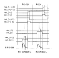
- FIG. 5 is a diagram for explaining a typical driving method by showing the voltage applied to each control line and the output voltage appearing on a vertical signal line in a certain column in the driving method of the present embodiment.
- the (i ⁇ 1) th and (i) th rows are for the row where the reading operation is performed, and the (i + j ⁇ 1) th to the (i + j + 1) th row for the row where the electronic shutter operation is performed.
- the driving period of the i-th row is the (i) scanning period ((i) H), and the driving period of the (i-1) -th row is the (i-1) -th scanning period ((i-1) H). ).
- res_ (i + j) is turned on to start the reset operation of the pixels in the (i + j) th row, and this state is changed to the (i + j + 1) th row in the (i) th scanning period. This is held until after the reset operation of the eye pixel is started. Thereafter, after sel_ (i + j) is turned on, res_ (i + j) is turned off, and sel_ (i + j) is turned off.
- the charge storage unit in the (i + j) th row is not subjected to potential fluctuation due to parasitic capacitance accompanying the start of the reset operation in the (i + j + 1) th row after the reset operation is completed until the start of reading. That is, no afterimage is generated.
- the reset of the pixels in the (i + j ⁇ 1) th row is switched from on to off during the (i ⁇ 1) th scanning period. Further, in FIG. 5, the (i-1) th row is read in the (i-1) th scanning period and the (i) th row is read in the (i) th scanning period by the same method as in FIG.
- the shutter period is j rows, but it is apparent in principle that this functions even if it exceeds the period of one frame.
- Embodiment 3 A solid-state imaging device according to Embodiment 3 of the present invention will be described with reference to FIGS. 6A and 6B.
- the configuration of the solid-state imaging device of this embodiment is the same as that in FIG. 1, and the cross-sectional structure of the pixel portion is the same as that in FIG.
- this is a case of driving for capturing a moving image without using an electronic shutter, that is, a rolling reset operation.
- the driving method shown in FIGS. 3A and 3B in Embodiment Mode 1 is applied in each scanning period, and an operation for sampling the reset signal may be added. It looks like this:
- sel_ (i) is turned on in the (i-1) th scanning period, and the pixel signal in the (i) th row is read. Thereafter, res_ (i) is turned on, and the reset operation of the (i) -th row is started.
- the time from res_ (i + 1) being turned on in the (i) th scanning period until res_ (i) is turned off is arbitrary, and the on / off operation of res_ (i + 1) is arbitrary. However, it must be on immediately before res_ (i) is turned off (exactly, a margin for the reaction time of the storage capacity is required).
- the time at which res_ (i) is turned on in advance is arbitrary (however, it is necessary to consider the reaction time of the charge storage unit or the like).
- sel_ (i) is turned on in the (i ⁇ 1) th scanning period, and the pixel signal in the (i) th row is read out. Thereafter, res_ (i) is turned on, and the reset operation of the (i) -th row is started. After maintaining this state for a time during which the pixel can be reset, res_ (i) is turned off.
- sel_ (i + 1) is turned on, and the pixel signal in the (i + 1) th row is read out. Thereafter, res_ (i + 1) is turned on, and the reset operation is started. After maintaining this state for a time during which the pixel can be reset, res_ (i + 1) is turned off. After that, sel_ (i) and res_ (i) are turned on, and (i) reset of the row is started (the sel_ (i) is not necessarily turned on. However, the transistor gate control line for selection and In order to suppress the influence of the parasitic component with the charge storage unit on the output signal, it is preferable to turn it on).
- res_ (i) is turned off, and the reset operation is terminated.
- the amount of charge in the charge accumulating portion on the (i + 1) th row does not substantially depend on the amount of light irradiation, so that afterimage can be prevented by this driving method according to the principle described in the first embodiment.
- the driving method described in this embodiment does not include reset signal readout.
- Embodiment 4 A solid-state imaging device according to Embodiment 4 of the present invention will be described with reference to FIGS.
- the configuration of the solid-state imaging device of this embodiment is the same as that of FIG. 1, and the cross-sectional structure of the pixel portion is the same as that of FIG.
- FIG. 7 schematically shows the pixel array 502 of the present embodiment, which is equivalent to FIG.
- Pixels in n rows (n is an integer of 2 or more) are arranged in the vertical scanning direction.
- the circuit diagram of each pixel is the same as that in FIG. 14, and the gate of the reset transistor 106 in each row is controlled by one reset control line in each row.
- the gate of the selection transistor 105 is controlled by a selection control line.
- Each row is numbered from 1 to n in the vertical scanning direction, the reset control line of the i-th row (i is an integer not less than 1 and not more than (n ⁇ 1)) is res_ (i), and the selection control line is sel_
- the notation (i) is the same as in FIG.
- signals are read out line by line in the illustrated direction (from bottom to top).
- a column amplifier 904 belonging to the column amplifier circuit 504 and a noise canceller circuit 905 for one column belonging to the noise canceller circuit 905 are shown.
- the noise canceller circuit 905 includes a first correlated double sampling circuit (first CDS circuit) including a switch 906, a capacitor 907, a switch 908, a capacitor 909, and a switch 910, a switch 911, a capacitor 912, a switch 913, and a capacitor 914.
- second CDS circuit comprising a switch 915 is connected in parallel.
- FIG. 8 is a diagram for explaining a typical driving method by showing the voltage applied to each control line and the output voltage appearing on a vertical signal line in a certain column in the driving method of the present embodiment.
- the i-th drive period is referred to as the (i) th scan period ((i) H)
- the (i + 1) th drive period is referred to as the (i + 1) th scan period ((i + 1) H).
- the second reset operation in the (i) th row is performed. Specifically, the switch 906 is turned on again, sel_ (i) and res_ (i) are turned on, and then turned off in the order of res_ (i) and sel_ (i).
- the vertical output signal V2 at this time is sampled by the first CDS circuit. Thereby, the difference between the previous sampling voltage V1 and this voltage V2 is obtained as the output voltage of the first CDS circuit. Thereafter, the output voltage of the CDS circuit obtained in each column is sequentially output to the outside of the solid-state imaging device by the horizontal driving circuit, and the driving in the (i) scanning period is finished. The same is true after the next (i + 1) th scanning period.
- the output voltage V1 in the next frame is obtained by adding only the voltage corresponding to the light intensity irradiated to each pixel that has no influence of the coupling of the reset operation to the output voltage V2 in the previous frame.
- the voltage (V1-V2) obtained by the CDS circuit is a true image signal that depends only on the light intensity. Therefore, also in the present embodiment, it is possible to capture a high-quality image with no afterimage.
- FIG. 9 is a block diagram showing a configuration of a solid-state imaging apparatus 1101 according to Embodiment 5 of the present invention.
- This solid-state imaging device 1101 includes a pixel array 1102, row signal drive circuits 1103a and 1103b, a column feedback circuit 1104 in which a circuit having an amplification and feedback function is arranged for each column, a column amplifier arranged in each column, A noise canceller circuit 1105 including a noise canceller, a horizontal drive circuit 1106, and an output stage amplifier 1107 are provided.
- the column feedback circuit 1104 receives and feeds back an output signal from the pixel array 1102. Therefore, the direction of signal flow is bidirectional with respect to the pixel array 1102 as shown in FIG.
- FIG. 10 is a circuit diagram showing a signal readout circuit of one pixel 1110 and its peripheral circuit included in the solid-state imaging device 1101.
- the pixel array 1102 includes a plurality of pixels 1110 arranged in a matrix, a plurality of column signal lines (vertical signal lines) 1204 provided for each column, and a plurality of row selection lines provided for each row. including.
- Each of the plurality of column signal lines 1204 is connected to a plurality of pixels 1110 arranged in the corresponding column.
- Each of the plurality of row selection lines is connected to a plurality of pixels 1110 arranged in the corresponding row.
- the pixel 1110 includes a photoelectric conversion unit 1201 and a signal readout circuit.
- the solid-state imaging device 1101 includes a column signal line 1204, a feedback amplifier 1205, a control circuit 1207 that controls an input level to the reset transistor 1206 according to an output from the feedback amplifier 1205, and an amplification transistor 1202.
- a transistor 1203, a column amplifier circuit 1212, a transistor 1210, and capacitors 1213 and 1214 are provided.
- the column signal line 1204, the feedback amplifier 1205, the control circuit 1207, the selection transistor 1203, the column amplification circuit 1212, the transistors 1210 and 1215, and the capacitors 1213 and 1214 are provided for each column.
- the photoelectric conversion unit 1201 generates signal charges corresponding to the amount of incident light by photoelectrically converting incident light.
- the signal read circuit generates a read signal corresponding to the signal charge generated by the photoelectric conversion unit 1201.
- This signal readout circuit includes an amplification transistor 1202, a selection transistor 1203, a reset transistor 1206, and an FD portion (floating diffusion portion) (not shown; the node voltage is described as V FD ).
- the amplification transistor 1202 detects the signal charge amount generated in the photoelectric conversion unit 1201.
- the selection transistor 1203 controls whether the signal detected by the amplification transistor 1202 is transmitted to the column signal line 1204.
- the reset transistor 1206 supplies a reset signal for resetting the photoelectric conversion unit 1201 and the FD unit to the FD unit.
- the control circuit 1207 controls the ON / OFF state of the reset transistor 1206 via the signal line in accordance with the output from the feedback amplifier 1205, and the photoelectric conversion unit controls the input level to the reset transistor 1206 via the signal line.
- 1201 is applied as a ground potential (hereinafter referred to as GND) or a high level potential (hereinafter referred to as V HIGH ).
- the selection transistor 1203 controls whether or not to transmit the pixel output signal V PIXO to the input terminal to the column amplifier circuit 1212.
- the transistor 1215 and the capacitors 1213 and 1214 are connected in series.
- the transistor 1215 controls whether or not the bias voltage V NCB is applied to the capacitor 1213.
- the signal amplified by the column amplifier circuit 1212 is input to a differential circuit including a transistor 1215 and capacitors 1213 and 1214. Then, the difference circuit detects a voltage corresponding to the signal by a difference operation.
- the configuration of the pixel array 1102 is the same as that in Embodiment 2 (FIG. 4).
- FIG. 11 is a diagram for explaining a typical driving method in the driving method according to the present embodiment by showing the voltage applied to each control line and the output voltage appearing on a vertical signal line in a certain column.
- the driving period of the i-th row is the (i) scanning period ((i) H)
- the driving period of the (i-1) -th row is the (i-1) -th scanning period ((i-1) H).
- the description will be made assuming that the noise canceller circuit 1105 has the same configuration as the noise canceller circuit 905.
- sel_ (i) is first turned on, and the selection transistor 1203 in the pixel on the (i) th row is turned on. Then, a voltage V 1 corresponding to the charge accumulated in the FD portion is generated by the amplification transistor 1202 and output to the column signal line 1204. This operation is performed with the switch 906 turned on, and sampling is performed by the first CDS circuit.
- the reset operation of the (i) line is started. Specifically, the switch 906 is turned off, res_ (i) is turned on, and the FD portion is reset by the reset transistor 1206 (a reset voltage is given to the reset transistor 1206 in advance by a voltage source or the like). Thereafter, res_ (i) is turned off to end the first reset operation in the (i) th row. At this time, the output after reset in the (i) th row is not sampled by the second CDS circuit.
- the second reset operation in the (i) th row is performed. Specifically, the switch 906 is turned on again, sel_ (i) and res_ (i) are turned on, and then turned off in the order of res_ (i) and sel_ (i).
- the vertical output signal V2 at this time is sampled by the first CDS circuit. Thereby, the difference between the previous sampling voltage V1 and this voltage V2 is obtained as the output voltage of the first CDS circuit. Thereafter, the output voltage of the CDS circuit obtained in each column is sequentially output to the outside of the solid-state imaging device by the horizontal driving circuit, and the driving in the (i) scanning period is finished. The same is true after the next (i + 1) th scanning period.
- the output voltage V1 in the next frame is obtained by adding only the voltage corresponding to the light intensity irradiated to each pixel that has no influence of the coupling of the reset operation to the output voltage V2 in the previous frame.
- the voltage (V1-V2) obtained by the CDS circuit is a true image signal that depends only on the light intensity. Therefore, also in the present embodiment, it is possible to capture a high-quality image with no afterimage.
- the reset operation is performed with the output fed back via the feedback amplifier 1205. With such a configuration, the inversion of the noise appearing at the output is fed back to the input, added with the positive sign component, and canceled.
- the reset signal is tapered at the end of the second reset in the (i) th row, so that a rapid reset operation is not performed.
- a rapid reset operation is not performed.
- This taper reset operation is not necessary in the present embodiment at the time of the first reset.
- the taper reset operation is performed. The higher noise reduction effect can be obtained.
- Embodiment 6 A solid-state imaging device driving method according to Embodiment 5 of the present invention will be described with reference to FIGS.
- the configuration of the solid-state imaging device of this embodiment is the same as that of FIG. 1, and the cross-sectional structure of the pixel portion is the same as that of FIG.
- FIG. 12 schematically shows the pixel array 502 of this embodiment, which is equivalent to FIG. Pixels in (2k) rows (2k and n are equal) are arranged in the vertical scanning direction.
- Pixels in (2k) rows (2k and n are equal) are arranged in the vertical scanning direction.
- it can be expressed as (2k + 1) rows.
- a is an integer of 0 to k.
- FIG. 13 is a diagram showing a driving method in the present embodiment.
- FIG. 13 shows so-called interlaced driving.
- An odd row signal is read in an odd frame and an even row signal is read in an even frame (the reverse combination is of course possible).
- the pixel signal of the (2a + 1) th row is read during the (a) scanning period.
- sel_ (2a + 1) is turned on, a voltage corresponding to the accumulated charge amount is read out to the vertical signal line, and is sampled by a CDS circuit or the like.
- res_ (2a + 1) is turned on to start the reset operation.
- the reset signal is read from the vertical signal line and sampled by a CDS circuit or the like.
- res_ (2a) is turned on, and the reset operation for the row (2a) is started.
- res_ (2a) is turned off and the reset operation is terminated.
- the reset operation of the (2a + 1) -th row since the reset operation of the (2a + 1) -th row has been completed and less than one scanning period has elapsed, the reset operation of the (2a) -th row hardly affects the light irradiation amount of the (2a + 1) -th row. Afterimages can be prevented.
- sel_ (2a) may be on or off (it is on in FIG. 13), but to the output signal of the parasitic component of the selection transistor gate control line and the storage capacitor. It is better to turn on to suppress the influence of.
- the (2a + 1) th row in the (a) scanning period in the odd frame described above is the (2a) row and the (2a) row is the (2a-1) row, respectively. Replace. With this operation, it is possible to secure an accumulation time of one frame and prevent afterimages.
- the present invention is not limited to these embodiments. Unless it deviates from the meaning of this invention, the form which carried out the various deformation
- the present invention is effective for digital still cameras, digital video cameras, and the like.
Abstract
Le but de la présente invention est de pourvoir à un procédé de pilotage d'un dispositif d'imagerie à semi-conducteurs apte à capturer une image de haute qualité sans la survenue d'un phénomène d'image résiduelle même lors de la capture d'une image animée avec un changement brusque de luminosité. Le dispositif d'imagerie à semi-conducteurs comprend des pixels agencés en une matrice bidimensionnelle ayant m colonnes dans une direction de balayage horizontale et n rangées dans une direction de balayage verticale, n étant un entier au moins égal à 2 et m étant un entier naturel. Lorsqu'une opération de réinitialisation pour les pixels de la ième rangée (i étant un entier allant de 1 à n-1 compris) est achevée, l'opération de réinitialisation pour les pixels de la (i+1)ième rangée est en cours ou le temps écoulé depuis l'achèvement de l'opération de réinitialisation pour les pixels de la (i+1)ième rangée est inférieur à la durée d'imagerie d'une image.
Priority Applications (3)
| Application Number | Priority Date | Filing Date | Title |
|---|---|---|---|
| JP2013508745A JP6011944B2 (ja) | 2011-04-08 | 2012-03-28 | 固体撮像装置の駆動方法 |
| CN201280015410.2A CN103444167B (zh) | 2011-04-08 | 2012-03-28 | 固体摄像装置的驱动方法 |
| US14/045,015 US9338383B2 (en) | 2011-04-08 | 2013-10-03 | Method for driving solid-state imaging device including starting/ending a reset operation on pixels arranged in a two-dimensional array |
Applications Claiming Priority (2)
| Application Number | Priority Date | Filing Date | Title |
|---|---|---|---|
| JP2011086842 | 2011-04-08 | ||
| JP2011-086842 | 2011-04-08 |
Related Child Applications (1)
| Application Number | Title | Priority Date | Filing Date |
|---|---|---|---|
| US14/045,015 Continuation US9338383B2 (en) | 2011-04-08 | 2013-10-03 | Method for driving solid-state imaging device including starting/ending a reset operation on pixels arranged in a two-dimensional array |
Publications (1)
| Publication Number | Publication Date |
|---|---|
| WO2012137445A1 true WO2012137445A1 (fr) | 2012-10-11 |
Family
ID=46968859
Family Applications (1)
| Application Number | Title | Priority Date | Filing Date |
|---|---|---|---|
| PCT/JP2012/002150 WO2012137445A1 (fr) | 2011-04-08 | 2012-03-28 | Procédé de pilotage de dispositif d'imagerie à semi-conducteurs |
Country Status (4)
| Country | Link |
|---|---|
| US (1) | US9338383B2 (fr) |
| JP (2) | JP6011944B2 (fr) |
| CN (1) | CN103444167B (fr) |
| WO (1) | WO2012137445A1 (fr) |
Cited By (2)
| Publication number | Priority date | Publication date | Assignee | Title |
|---|---|---|---|---|
| KR20160008632A (ko) | 2013-06-04 | 2016-01-22 | 후지필름 가부시키가이샤 | 고체 촬상 소자 및 촬상 장치 |
| US10079988B2 (en) | 2015-07-07 | 2018-09-18 | Panasonic Intellectual Property Management Co., Ltd. | Imaging device including pixel |
Families Citing this family (3)
| Publication number | Priority date | Publication date | Assignee | Title |
|---|---|---|---|---|
| FR3000347B1 (fr) * | 2012-12-21 | 2016-03-04 | Trixell | Procede de lecture d'un dispositif d'imagerie |
| JP6045382B2 (ja) * | 2013-02-13 | 2016-12-14 | オリンパス株式会社 | 固体撮像装置 |
| WO2020217783A1 (fr) * | 2019-04-25 | 2020-10-29 | パナソニックIpマネジメント株式会社 | Dispositif d'imagerie |
Citations (3)
| Publication number | Priority date | Publication date | Assignee | Title |
|---|---|---|---|---|
| JP2000253314A (ja) * | 1999-03-03 | 2000-09-14 | Olympus Optical Co Ltd | 固体撮像装置の駆動方法 |
| JP2009177378A (ja) * | 2008-01-23 | 2009-08-06 | Olympus Corp | 固体撮像装置 |
| JP2010183558A (ja) * | 2009-01-07 | 2010-08-19 | Sony Corp | 固体撮像素子および駆動制御方法 |
Family Cites Families (12)
| Publication number | Priority date | Publication date | Assignee | Title |
|---|---|---|---|---|
| JPS5850030B2 (ja) | 1979-03-08 | 1983-11-08 | 日本放送協会 | 光電変換装置およびそれを用いた固体撮像板 |
| JPS5850030A (ja) | 1981-09-21 | 1983-03-24 | Mitsubishi Electric Corp | 電子計算機システムの電源制御装置 |
| JPH05161073A (ja) * | 1991-12-06 | 1993-06-25 | Hamamatsu Photonics Kk | 固体撮像装置 |
| JP3693281B2 (ja) * | 1999-09-30 | 2005-09-07 | シャープ株式会社 | 増幅型固体撮像装置 |
| US20040036784A1 (en) * | 2002-08-23 | 2004-02-26 | Bock Nikolai E. | High dynamic range pixel with gain and true shutter capability |
| JP4510523B2 (ja) * | 2004-06-02 | 2010-07-28 | キヤノン株式会社 | 固体撮像装置および撮像システム |
| JP4325557B2 (ja) * | 2005-01-04 | 2009-09-02 | ソニー株式会社 | 撮像装置および撮像方法 |
| JP2007013245A (ja) * | 2005-06-28 | 2007-01-18 | Sony Corp | 固体撮像装置、固体撮像装置の駆動方法および撮像装置 |
| JP2007060350A (ja) * | 2005-08-25 | 2007-03-08 | Matsushita Electric Ind Co Ltd | イメージセンサ |
| JP5255790B2 (ja) * | 2007-02-14 | 2013-08-07 | 富士フイルム株式会社 | 撮像装置 |
| JP2011030060A (ja) * | 2009-07-28 | 2011-02-10 | Olympus Corp | 固体撮像装置および撮像方法 |
| JP4444371B1 (ja) | 2009-09-01 | 2010-03-31 | 富士フイルム株式会社 | 撮像素子及び撮像装置 |
-
2012
- 2012-03-28 CN CN201280015410.2A patent/CN103444167B/zh active Active
- 2012-03-28 JP JP2013508745A patent/JP6011944B2/ja active Active
- 2012-03-28 WO PCT/JP2012/002150 patent/WO2012137445A1/fr active Application Filing
-
2013
- 2013-10-03 US US14/045,015 patent/US9338383B2/en active Active
-
2016
- 2016-09-08 JP JP2016175979A patent/JP6191978B2/ja active Active
Patent Citations (3)
| Publication number | Priority date | Publication date | Assignee | Title |
|---|---|---|---|---|
| JP2000253314A (ja) * | 1999-03-03 | 2000-09-14 | Olympus Optical Co Ltd | 固体撮像装置の駆動方法 |
| JP2009177378A (ja) * | 2008-01-23 | 2009-08-06 | Olympus Corp | 固体撮像装置 |
| JP2010183558A (ja) * | 2009-01-07 | 2010-08-19 | Sony Corp | 固体撮像素子および駆動制御方法 |
Cited By (3)
| Publication number | Priority date | Publication date | Assignee | Title |
|---|---|---|---|---|
| KR20160008632A (ko) | 2013-06-04 | 2016-01-22 | 후지필름 가부시키가이샤 | 고체 촬상 소자 및 촬상 장치 |
| US10079988B2 (en) | 2015-07-07 | 2018-09-18 | Panasonic Intellectual Property Management Co., Ltd. | Imaging device including pixel |
| US10440302B2 (en) | 2015-07-07 | 2019-10-08 | Panasonic Intellectual Property Management Co., Ltd. | Imaging device including pixel |
Also Published As
| Publication number | Publication date |
|---|---|
| JP6191978B2 (ja) | 2017-09-06 |
| US20140027619A1 (en) | 2014-01-30 |
| US9338383B2 (en) | 2016-05-10 |
| JP2017005754A (ja) | 2017-01-05 |
| CN103444167B (zh) | 2017-09-29 |
| CN103444167A (zh) | 2013-12-11 |
| JPWO2012137445A1 (ja) | 2014-07-28 |
| JP6011944B2 (ja) | 2016-10-25 |
Similar Documents
| Publication | Publication Date | Title |
|---|---|---|
| US11159756B2 (en) | Solid-state image pickup element and image pickup system | |
| JP5326751B2 (ja) | 固体撮像装置、固体撮像装置の信号処理方法および電子機器 | |
| JP5251736B2 (ja) | 固体撮像装置、固体撮像装置の駆動方法および電子機器 | |
| JP6191978B2 (ja) | 固体撮像装置の駆動方法 | |
| JP5821315B2 (ja) | 電子機器、電子機器の駆動方法 | |
| TWI533699B (zh) | A solid-state imaging element and a driving method, and an electronic device | |
| WO2015072575A1 (fr) | Élément d'imagerie à semi-conducteurs et dispositif d'imagerie | |
| KR20150002593A (ko) | 고체 촬상 장치 및 전자 기기 | |
| JP6413401B2 (ja) | 固体撮像素子 | |
| JP2013005396A (ja) | 固体撮像装置、固体撮像装置の駆動方法、及び電子機器 | |
| TW201541963A (zh) | 固體攝像裝置 | |
| JP2012227889A (ja) | 固体撮像装置 | |
| JP2011055345A (ja) | 撮像装置 | |
| JP6733159B2 (ja) | 撮像素子、及び撮像装置 | |
| JP6217338B2 (ja) | 固体撮像素子及び撮像装置 | |
| JP6256054B2 (ja) | 固体撮像素子及び撮像装置 | |
| JP6702371B2 (ja) | 撮像素子及び撮像装置 | |
| JP2008177593A (ja) | 固体撮像素子及びカメラ装置 | |
| JP6375613B2 (ja) | 固体撮像素子及び撮像装置 | |
| JP7160129B2 (ja) | 撮像素子および撮像装置 | |
| JP7198675B2 (ja) | 固体撮像素子、その駆動回路および撮像装置 | |
| JP7439772B2 (ja) | 撮像素子及び撮像装置 | |
| JP5299496B2 (ja) | 固体撮像素子及びカメラ装置 | |
| JP2017220957A (ja) | 固体撮像素子及び撮像装置 | |
| JP2020170953A (ja) | 撮像装置および画像フレーム読出し制御回路 |
Legal Events
| Date | Code | Title | Description |
|---|---|---|---|
| 121 | Ep: the epo has been informed by wipo that ep was designated in this application |
Ref document number: 12767998 Country of ref document: EP Kind code of ref document: A1 |
|
| ENP | Entry into the national phase |
Ref document number: 2013508745 Country of ref document: JP Kind code of ref document: A |
|
| NENP | Non-entry into the national phase |
Ref country code: DE |
|
| 122 | Ep: pct application non-entry in european phase |
Ref document number: 12767998 Country of ref document: EP Kind code of ref document: A1 |