WO2012137445A1 - Method for driving solid-state imaging device - Google Patents
Method for driving solid-state imaging device Download PDFInfo
- Publication number
- WO2012137445A1 WO2012137445A1 PCT/JP2012/002150 JP2012002150W WO2012137445A1 WO 2012137445 A1 WO2012137445 A1 WO 2012137445A1 JP 2012002150 W JP2012002150 W JP 2012002150W WO 2012137445 A1 WO2012137445 A1 WO 2012137445A1
- Authority
- WO
- WIPO (PCT)
- Prior art keywords
- row
- reset
- state imaging
- pixel
- imaging device
- Prior art date
Links
- 238000003384 imaging method Methods 0.000 title claims abstract description 84
- 238000000034 method Methods 0.000 title claims abstract description 64
- 238000009825 accumulation Methods 0.000 claims description 12
- 230000008859 change Effects 0.000 abstract description 7
- 239000011159 matrix material Substances 0.000 abstract description 3
- 239000003990 capacitor Substances 0.000 description 31
- 238000010586 diagram Methods 0.000 description 31
- 238000006243 chemical reaction Methods 0.000 description 28
- 206010047571 Visual impairment Diseases 0.000 description 22
- 239000010410 layer Substances 0.000 description 21
- 230000000875 corresponding effect Effects 0.000 description 16
- 239000000758 substrate Substances 0.000 description 14
- 230000003321 amplification Effects 0.000 description 13
- 238000003199 nucleic acid amplification method Methods 0.000 description 13
- 238000005070 sampling Methods 0.000 description 12
- 230000008878 coupling Effects 0.000 description 9
- 238000010168 coupling process Methods 0.000 description 9
- 238000005859 coupling reaction Methods 0.000 description 9
- 230000003071 parasitic effect Effects 0.000 description 9
- 230000000903 blocking effect Effects 0.000 description 6
- 239000000470 constituent Substances 0.000 description 5
- 238000002955 isolation Methods 0.000 description 4
- 239000004065 semiconductor Substances 0.000 description 4
- 230000002596 correlated effect Effects 0.000 description 3
- 230000001681 protective effect Effects 0.000 description 3
- 238000009792 diffusion process Methods 0.000 description 2
- 230000000694 effects Effects 0.000 description 2
- 239000011229 interlayer Substances 0.000 description 2
- 230000031700 light absorption Effects 0.000 description 2
- 229910044991 metal oxide Inorganic materials 0.000 description 2
- 150000004706 metal oxides Chemical class 0.000 description 2
- 230000008569 process Effects 0.000 description 2
- 230000035484 reaction time Effects 0.000 description 2
- 230000009467 reduction Effects 0.000 description 2
- 229910004298 SiO 2 Inorganic materials 0.000 description 1
- XUIMIQQOPSSXEZ-UHFFFAOYSA-N Silicon Chemical compound [Si] XUIMIQQOPSSXEZ-UHFFFAOYSA-N 0.000 description 1
- ATJFFYVFTNAWJD-UHFFFAOYSA-N Tin Chemical compound [Sn] ATJFFYVFTNAWJD-UHFFFAOYSA-N 0.000 description 1
- 239000011358 absorbing material Substances 0.000 description 1
- 230000002457 bidirectional effect Effects 0.000 description 1
- 230000000295 complement effect Effects 0.000 description 1
- 230000007423 decrease Effects 0.000 description 1
- 238000007599 discharging Methods 0.000 description 1
- AMGQUBHHOARCQH-UHFFFAOYSA-N indium;oxotin Chemical compound [In].[Sn]=O AMGQUBHHOARCQH-UHFFFAOYSA-N 0.000 description 1
- 238000002347 injection Methods 0.000 description 1
- 239000007924 injection Substances 0.000 description 1
- 239000000463 material Substances 0.000 description 1
- 230000007246 mechanism Effects 0.000 description 1
- 230000003287 optical effect Effects 0.000 description 1
- 230000002093 peripheral effect Effects 0.000 description 1
- 238000005096 rolling process Methods 0.000 description 1
- 229910052710 silicon Inorganic materials 0.000 description 1
- 239000010703 silicon Substances 0.000 description 1
- 239000007787 solid Substances 0.000 description 1
- 230000009466 transformation Effects 0.000 description 1
- 238000001771 vacuum deposition Methods 0.000 description 1
Images


Classifications
-
- H—ELECTRICITY
- H04—ELECTRIC COMMUNICATION TECHNIQUE
- H04N—PICTORIAL COMMUNICATION, e.g. TELEVISION
- H04N25/00—Circuitry of solid-state image sensors [SSIS]; Control thereof
- H04N25/70—SSIS architectures; Circuits associated therewith
- H04N25/71—Charge-coupled device [CCD] sensors; Charge-transfer registers specially adapted for CCD sensors
- H04N25/75—Circuitry for providing, modifying or processing image signals from the pixel array
-
- H—ELECTRICITY
- H04—ELECTRIC COMMUNICATION TECHNIQUE
- H04N—PICTORIAL COMMUNICATION, e.g. TELEVISION
- H04N25/00—Circuitry of solid-state image sensors [SSIS]; Control thereof
- H04N25/60—Noise processing, e.g. detecting, correcting, reducing or removing noise
- H04N25/62—Detection or reduction of noise due to excess charges produced by the exposure, e.g. smear, blooming, ghost image, crosstalk or leakage between pixels
- H04N25/626—Reduction of noise due to residual charges remaining after image readout, e.g. to remove ghost images or afterimages
-
- H—ELECTRICITY
- H04—ELECTRIC COMMUNICATION TECHNIQUE
- H04N—PICTORIAL COMMUNICATION, e.g. TELEVISION
- H04N25/00—Circuitry of solid-state image sensors [SSIS]; Control thereof
- H04N25/70—SSIS architectures; Circuits associated therewith
- H04N25/71—Charge-coupled device [CCD] sensors; Charge-transfer registers specially adapted for CCD sensors
- H04N25/745—Circuitry for generating timing or clock signals
-
- H—ELECTRICITY
- H04—ELECTRIC COMMUNICATION TECHNIQUE
- H04N—PICTORIAL COMMUNICATION, e.g. TELEVISION
- H04N25/00—Circuitry of solid-state image sensors [SSIS]; Control thereof
- H04N25/70—SSIS architectures; Circuits associated therewith
- H04N25/76—Addressed sensors, e.g. MOS or CMOS sensors
- H04N25/78—Readout circuits for addressed sensors, e.g. output amplifiers or A/D converters
-
- H—ELECTRICITY
- H01—ELECTRIC ELEMENTS
- H01L—SEMICONDUCTOR DEVICES NOT COVERED BY CLASS H10
- H01L27/00—Devices consisting of a plurality of semiconductor or other solid-state components formed in or on a common substrate
- H01L27/14—Devices consisting of a plurality of semiconductor or other solid-state components formed in or on a common substrate including semiconductor components sensitive to infrared radiation, light, electromagnetic radiation of shorter wavelength or corpuscular radiation and specially adapted either for the conversion of the energy of such radiation into electrical energy or for the control of electrical energy by such radiation
- H01L27/144—Devices controlled by radiation
- H01L27/146—Imager structures
- H01L27/14601—Structural or functional details thereof
- H01L27/14609—Pixel-elements with integrated switching, control, storage or amplification elements
Definitions
- the present invention relates to a method for driving a solid-state imaging device that outputs an image as an electrical signal.
- CMOS Complementary Metal Oxide Semiconductor
- MOS Metal Oxide Semiconductor
- CCD image sensor charge-coupled device CCD image sensor
- a conventional solid-state imaging device has a configuration in which pixels having a photoelectric conversion unit (photodiode) and a readout circuit unit are arranged in a two-dimensional array on the outermost surface of a semiconductor substrate. Therefore, the area of the photoelectric conversion unit is reduced by the area of the readout circuit unit on the light incident surface. As a result, the conventional solid-state imaging device has a problem that the aperture ratio decreases.
- Patent Document 1 and Patent Document 2 disclose stacked solid-state imaging devices each including a photoelectric conversion unit having a structure in which a light-absorbing material is stacked on a substrate and a readout circuit formed on the substrate. It has been reported.
- the photoelectric conversion unit of each pixel includes a pixel electrode, a photoelectric conversion film stacked above (light incident side), and a counter electrode formed on the upper surface thereof. including.
- the multilayer solid-state imaging device takes out a charge group generated by incident light as a current signal outside the photoelectric conversion unit via the pixel electrode.
- the stacked solid-state imaging device usually includes a charge blocking layer that conducts signal charges to select a sign of signal charges and blocks charges of opposite signs. The charge blocking layer faces the pixel electrode or is in direct contact with the pixel electrode.
- FIG. 14 schematically shows a circuit of a pixel portion (pixel) of a conventional stacked image sensor using an organic film described in Patent Document 1 as a photoelectric conversion film.
- the signal charge output from the photoelectric conversion unit 101 through the pixel electrode 102 is stored in the charge storage unit 103 formed of a depletion layer capacitance formed on the substrate.
- the charge storage unit 103 is connected to an input gate of a pixel readout transistor (amplification transistor) 104 via a wiring, and a selection transistor 105 that detects a change in voltage associated with a change in the amount of stored charge and selects a readout timing of the pixel.
- amplification transistor amplification transistor
- the drain part of the reset transistor 106 is connected to the charge storage part 103 in order to reset the charge of the charge storage part 103, and the charge storage part voltage is set to the initial state voltage at the time of reset. Is set.
- FIG. 15 schematically shows a stacked solid-state imaging device in which the pixels of FIG. 14 are two-dimensionally arranged, and n rows (n is an integer of 2 or more) of pixels are arranged in the vertical scanning direction. ing.
- the gates of the reset transistors 106 in each row are controlled by one reset control line for each row.
- the gate of the selection transistor 105 is controlled by a selection control line.
- Each row is numbered from 1 to n in the vertical scanning direction, the reset control line of the i-th row (i is an integer not less than 1 and not more than (n ⁇ 1)) is res_ (i), and the selection control line is sel_ (I) and a typical driving method of the multilayer solid-state imaging device at the time of moving image shooting will be described with reference to FIG.
- FIG. 16 is a diagram for explaining a typical driving method by showing a voltage applied to each control line and an output voltage appearing on a vertical signal line 107 in a certain column.
- FIG. 16 only the (i ⁇ 1) th to (i + 1) th rows are shown, but if the same driving is sequentially performed from the first to nth rows, an image signal for one screen can be obtained. Since it can be easily understood by those skilled in the art, it is omitted.
- the driving period (horizontal scanning period) of the i-th row is described as the (i) th scanning period.
- res_ (i ⁇ 1) is turned on, and the charge accumulation unit 103 is reset by the reset transistor 106 (a reset voltage is given to the reset transistor 106 in advance by a voltage source or the like). Thereafter, res_ (i-1) is turned off to complete the reset operation of the (i-1) th row, and the voltage V2 (referred to as a reset signal) output to the vertical signal line 107 is output by a CDS circuit or the like. Sampling is performed (this operation is hereinafter referred to as “reset signal reading”). Thereby, the difference between the sampling voltage V1 and the voltage V2 is obtained as the output voltage of the CDS circuit.
- the output voltage of the CDS circuit obtained in each column is sequentially output to the outside of the solid-state imaging device by the horizontal transfer circuit, and the driving in the (i-1) th scanning period is finished.
- the same driving is performed even after the next (i) scanning period.
- the same driving is repeated from the (1) th scanning period of the next frame.
- the output voltage V1 in the next frame is obtained by adding the voltage corresponding to the light intensity irradiated to each pixel to the output voltage V2 in the previous frame, and thus the voltage (V1-V2) obtained by the CDS circuit. ) Is a true image signal depending only on the light intensity.
- FIG. 17 is a diagram showing two pixels in the i-th row and the (i + 1) -th row adjacent in the vertical scanning direction, and the configuration of each pixel is the same as that in FIG. However, in FIG. 17, a parasitic capacitance 108 between these pixels is added.
- the parasitic capacitance 108 is generated between the pixel electrodes 102, between the gate wirings of the pixel readout transistor 104, and the like.
- the value of the charge storage unit (storage capacitor) 103 is Ca (this is usually the same value for all pixels), and the value of the parasitic capacitor 108 is Cp.
- Vres (i) the voltage of the storage capacitor 103 (i) after the reset operation of the (i) th row is completed, that is, immediately after res_ (i) is turned off, is Vres (i).
- the voltage of the storage capacitor 103 (i + 1) at this time is set to Vfd1 (i + 1).
- Vres1 (i) is determined by the reset voltage applied to the reset transistor 106 (i), the threshold value of the reset transistor 106 (i), and the gate-drain capacitance (assuming the storage capacitor 103 side is the drain), and is applied to the pixel. It does not depend on the light intensity.
- Vfd1 (i + 1) depends on the light intensity applied to the pixels in the (i + 1) th row.
- ⁇ is a value that depends on the selection transistor 105 and other parasitic capacitances, and does not depend on the amount of light irradiation.
- the voltage of the storage capacitor 103 (i) when the selection transistor 105 (i) is turned on is substantially equal to the sum of Qa and Vres2 (i).
- the voltage value is Vout (i)
- Vout (i) depends on Vfd1 (i + 1), which appears as an afterimage. For example, if the intensity of light irradiated to the (i + 1) th row in the previous frame is high, the value of Vout (i) becomes small depending on it. As an image, a black and white inverted version of the image of the previous frame is superimposed on the current frame. Note that ⁇ is a value due to a parasitic component similar to ⁇ .
- the present invention has been made in view of the above-described prior art, and provides a driving method of a solid-state imaging device that enables high-quality imaging without occurrence of an afterimage phenomenon even when capturing moving images with a sharp change in luminance. With the goal.
- a driving method of a solid-state imaging device includes pixels arranged in a two-dimensional array of m columns in the horizontal scanning direction and n rows in the vertical scanning direction.
- This is a driving method of the solid-state imaging device (n is an integer of 2 or more, m is a natural number), and the reset operation of the pixel in the i-th row (i is an integer of 1 to n-1) is completed.
- the pixel in the (i + 1) th row is being reset, or the elapsed time after the pixel in the (i + 1) th row has finished the reset operation is less than one frame imaging time.
- the potential fluctuation of the output signal due to coupling of the reset operation of the row adjacent to the predetermined row does not occur. Therefore, no afterimage occurs between frames.
- the driving method of the solid-state imaging device includes an accumulation time of j horizontal scanning periods (j is an integer of 1 to (n ⁇ 1)).
- j is an integer of 1 to (n ⁇ 1)
- the driving method of the solid-state imaging device is to read out pixel signals of the (i + 1) -th row (i is an integer of 1 to n-1).
- the operation, the start of the reset operation of the (i + 1) -th row, and the end of the reset operation of the i-th row are sequentially performed.
- the potential fluctuation of the output signal due to the coupling of the reset operation of the adjacent row can be removed by the second reset operation, so that no afterimage is generated between frames.
- the driving method of the solid-state imaging device is to read out pixel signals of the (i + 1) -th row (i is an integer of 1 to n-1).
- the operation, the start of the reset operation of the (i + 1) th row, the end of the reset operation of the (i + 1) th row, the reset signal reading operation of the (i + 1) th row, and the end of the reset operation of the ith row are sequentially performed. It is characterized by performing.
- the potential fluctuation of the output signal due to the coupling of the reset operation of the adjacent row can be removed by the second reset operation, so that no afterimage is generated between frames.
- the driving method of the solid-state imaging device is to read out pixel signals of the (i + 1) -th row (i is an integer of 1 to n-1).
- the operation, the start of the reset operation of the (i + 1) th row, the end of the reset operation of the i row, and the reset signal read operation of the i row are sequentially performed.
- the potential fluctuation of the output signal due to the coupling of the reset operation of the adjacent row can be removed by the second reset operation, so that no afterimage is generated between frames.
- a driving method of a solid-state imaging device is a two-dimensional form of m columns in the horizontal scanning direction and 2k rows or (2k + 1) rows in the vertical scanning direction.
- a + 1) -th pixel signal (a is an integer of 0 to k) Operation, driving of the odd-numbered frame in which the reset operation of the (2a + 1) th row, the reset signal reading operation of the (2a + 1) th row, and the reset operation of the 2a row are sequentially performed, and the pixel signal reading of the (2a + 2) th row And an even-numbered frame driving in which the reset operation of the (2a + 2) th row, the reset signal reading operation of the (2a + 2) th row, and the reset operation of the (2a + 1) th row are sequentially performed.
- a driving method of the imaging apparatus can be provided.
- FIG. 1 is a diagram illustrating each part of the stacked solid-state imaging device according to Embodiment 1 of the present invention.
- FIG. 2 is a cross-sectional view of the solid-state imaging device according to Embodiment 1 of the present invention.
- FIG. 3A is a diagram illustrating a method for driving the solid-state imaging device according to Embodiment 1 of the present invention.
- FIG. 3B is a diagram illustrating a method for driving the solid-state imaging device according to Embodiment 1 of the present invention.
- FIG. 4 is a diagram for explaining the solid-state imaging device according to the second embodiment of the present invention.
- FIG. 5 is a diagram illustrating a method for driving the solid-state imaging device according to the second embodiment of the present invention.
- FIG. 6A is a diagram illustrating a method for driving the solid-state imaging device according to Embodiment 3 of the present invention.
- FIG. 6B is a diagram illustrating a method for driving the solid-state imaging device according to Embodiment 3 of the present invention.
- FIG. 7 is a diagram for explaining the solid-state imaging device according to the fourth embodiment of the present invention.
- FIG. 8 is a diagram illustrating a driving method of the solid-state imaging device according to the fourth embodiment of the present invention.
- FIG. 9 is a diagram illustrating a solid-state imaging device according to Embodiment 5 of the present invention.
- FIG. 10 is a diagram for explaining the solid-state imaging device according to the fifth embodiment of the present invention.
- FIG. 10 is a diagram for explaining the solid-state imaging device according to the fifth embodiment of the present invention.
- FIG. 11 is a diagram for explaining a driving method of the solid-state imaging device according to the fifth embodiment of the present invention.
- FIG. 12 is a diagram illustrating a solid-state imaging device according to Embodiment 6 of the present invention.
- FIG. 13 is a diagram for explaining a driving method of the solid-state imaging device according to the sixth embodiment of the present invention.
- FIG. 14 is a diagram illustrating pixels of a conventional stacked solid-state imaging device.
- FIG. 15 is a diagram illustrating a pixel array of the solid-state imaging device.
- FIG. 16 is a diagram illustrating a method for driving the solid-state imaging device.
- FIG. 17 is a diagram illustrating a pixel portion of the solid-state imaging device.
- Embodiment 1 A method for driving the solid-state imaging device according to Embodiment 1 of the present invention will be described with reference to FIGS. 1 to 3B.
- FIG. 1 is a block diagram showing a configuration of a solid-state imaging device 501 according to Embodiment 1 of the present invention.
- the solid-state imaging device 501 includes a pixel array 502, row signal driving circuits 503a and 503b, a column amplifier circuit 504 arranged for each column, a noise canceller circuit 505 arranged for each column, a horizontal driving circuit 506, And an output stage amplifier 507.
- FIG. 2 is a cross-sectional view of an area corresponding to three pixels of the solid-state imaging device 501.
- the actual pixels are arranged in the pixel array 502, for example, for 10 million pixels.
- the circuit diagram of each pixel is the same as FIG.
- the solid-state imaging device 501 includes a microlens 601, a red color filter 602, a green color filter 603, a blue color filter 604, a protective film 605, a planarization film 606, and an upper electrode 607.
- photoelectric conversion film 608 electron blocking layer 609
- interelectrode insulating film 610 lower electrode 611 (first electrode)
- interwiring insulating film 612 feeding layer 613, wiring layer 614, a substrate 618, a well 619, an STI region (shallow trench isolation region) 620, and an interlayer insulating layer 621.
- the substrate 618 is a semiconductor substrate, for example, a silicon substrate.
- a signal readout circuit for reading out signal charges generated by photoelectric conversion of the photoelectric conversion film 608 to the outside of the pixel as a signal voltage (readout signal), that is, a plurality of transistors (amplification transistor 616, selection transistor, and reset) Transistor 617) is formed.
- the micro lens 601 is formed for each pixel 510 on the outermost surface of the solid-state imaging device 501 in order to efficiently collect incident light.
- the red color filter 602, the green color filter 603, and the blue color filter 604 are formed for capturing a color image. Further, the red color filter 602, the green color filter 603, and the blue color filter 604 are formed immediately below each microlens 601 and in the protective film 605. These optical elements are formed on the planarizing film 606 in order to form a microlens 601 and a color filter group free from unevenness of color collection and color over 10 million pixels.
- the planarizing film 606 is made of SiN, for example.
- the upper electrode 607 is formed under the planarizing film 606 over the entire surface of the pixel array 502.
- the upper electrode 607 transmits visible light.
- the upper electrode 607 is made of ITO (Indium Tin Oxide).
- the photoelectric conversion film 608 converts light into signal charges. Specifically, the photoelectric conversion film 608 is formed under the upper electrode 607 and is composed of organic molecules having high light absorption ability. Moreover, the thickness of the photoelectric conversion film 608 is, for example, 500 nm. Further, the photoelectric conversion film 608 is formed by using a vacuum evaporation method. The organic molecule has a high light absorption ability over the entire visible light having a wavelength of 400 nm to 700 nm.
- the electron blocking layer 609 is formed under the photoelectric conversion film 608 and conducts holes generated by photoelectric conversion of incident light and blocks injection of electrons from the lower electrode 611.
- the electron blocking layer 609 is formed on the interelectrode insulating film 610 and the lower electrode 611 having high flatness.
- the plurality of lower electrodes 611 are arranged in a matrix above the substrate 618.
- the plurality of lower electrodes 611 are electrically isolated from each other.
- the lower electrode 611 is formed between the interelectrode insulating films 610 and collects holes generated in the photoelectric conversion film 608.
- the lower electrode 611 is made of, for example, TiN.
- the lower electrode 611 is formed on the planarized inter-wiring insulating film 612 having a thickness of 100 nm.
- the lower electrodes 611 are separated by an interval of 0.2 ⁇ m.
- An interelectrode insulating film 610 is also embedded in this isolation region.
- a power feeding layer 613 is disposed below the isolation region and below the inter-wiring insulating film 612.
- the power supply layer 613 is made of Cu, for example.
- the power feeding layer 613 is a region between the adjacent lower electrodes 611 and is formed between the lower electrode 611 and the substrate 618.
- a potential independent of the lower electrode 611 can be supplied to the power feeding layer 613.
- a potential for discharging signal charges is supplied to the power supply layer 613 during an exposure operation in which the photoelectric conversion film 608 performs photoelectric conversion and in a read operation in which the signal read circuit generates a read signal.
- a positive voltage is applied. Thereby, it can prevent that a hole mixes into each pixel from an adjacent pixel.
- Such voltage application control is performed, for example, by a control unit (not shown) included in the solid-state imaging device 501.
- a wiring layer 614 is connected to the power feeding layer 613.
- the wiring layer 614 is connected to the FD portion (charge storage portion) 615 and the gate terminal of the amplification transistor 616 of the signal readout circuit.
- the FD portion 615 is electrically connected to the source terminal of the reset transistor 617.
- the source terminal of the reset transistor 617 and the FD unit 615 share a diffusion region.
- These transistors, a selection transistor (not shown) formed in the same pixel, and the FD portion 615 are all formed in the same P-type well 619.
- the well 619 is formed on the substrate 618.
- the signal readout circuit is formed on the substrate 618 and generates a readout signal corresponding to the signal charge by detecting a change in current or voltage generated in each of the plurality of lower electrodes 611.
- the amplification transistor 616 generates a read signal by amplifying a change in current or voltage generated in the lower electrode 611.
- each transistor is electrically isolated by configured STI region 620 in SiO 2.
- the gate terminal of the reset transistor 617 is connected to the reset control line, and the on / off of the reset transistor 617 is controlled by the potential of the reset control line. For example, when the potential of the reset control line is set to a high level and the reset control line is turned on, the reset transistor 617 is turned on, and the potential of the reset control line is set to a low level and the reset control line is turned off. The reset transistor 617 is turned off.
- the gate terminal of the selection transistor is connected to the selection control line, and the on / off of the selection transistor is controlled by the potential of the selection control line. For example, when the potential of the selection control line is set to high level and the selection control line is turned on, the selection transistor is turned on, and when the potential of the selection control line is set to low level and the selection control line is turned off, The selection transistor is turned off.
- the configuration of the pixel array 502 of this embodiment is the same as that in FIG. 16, and n rows (n is an integer of 2 or more) in the vertical scanning direction and m rows (m is a natural number) are arranged in the horizontal direction. Has been.
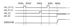
- FIG. 3A and 3B are diagrams showing a driving method of the solid-state imaging device in the present embodiment. This shows the signals given to each control line in time series. Further, although only the i-th and (i + 1) -th lines are shown, it is easy for those skilled in the art to apply this to the normal vertical scanning operation.
- the reset control line in the i-th row is referred to as res_ (i), and the selection control line is referred to as sel_ (i).
- FIG. 3A will be described.
- res_ (i) is turned on to start the reset operation of the i-th row.
- the voltage of the FD portion 615 (storage capacitor 103 (i + 1)) in the (i + 1) th row at time b is Vfd2 (i + 1), and the FD in the (i + 1) th row at time c.
- the voltage of the unit 615 (storage capacitor 103 (i + 1)) is Vfd3 (i + 1)
- the voltage of the FD unit 615 (storage capacitor 103 (i)) in the (i) th row is as follows.
- Vfd2 (i + 1) is a value immediately after reset during reset operation of the (i + 1) th row, and does not depend on the light irradiation amount. If time b in FIG. 3A is the previous frame of time d, which is the time of reading, no matter what light irradiation state was in the previous frame, an output independent of it will be obtained at time d, The afterimage removal which is the subject of the present invention can be achieved. Actually, if the solid-state imaging device is driven so as to satisfy the driving method shown in FIG. 3A described above (this example is shown in the following embodiment), the afterimage can be removed.
- FIG. 3B shows another driving method.
- res_ (i + 1) is turned off at time a ′, and the reset of the (i + 1) th row is completed.
- res_ (i + 1) is turned off at time c, and reset of the (i + 1) -th row is completed (res_ (i + 1) is turned on before time c).
- the operation at time d is the same as the driving method of FIG. 3A.
- the voltage of the FD unit 615 (storage capacitor 103 (i + 1)) in the (i) th row at time b is Vfd2 (i + 1) ′, and the FD unit 615 (storage capacitor 103 (i + 1) in the (i + 1) th row at time c. ) Is Vfd3 (i + 1) ′, the output voltage at time d is considered in the same way as in FIG. 3A.
- Vfd2 (i + 1) ′ depends on the light irradiation amount. However, if the time difference between the time a ′ and the time b is shortened, it can be made almost independent. A shorter time difference is better, for example, one scanning period. At least, it is necessary to make it less than one frame accumulation time (one frame accumulation time is the same as the normal driving method). Since Vfd3 (i + 1) ′ is immediately after reset and does not depend on the amount of light irradiation, this method can similarly remove the afterimage.
- sel_ (i) must be turned on only at time d, and may be turned on or off at time b.
- the voltage of the FD section 615 (storage capacitor 103_ (i + 1)) in the (i + 1) th row is set to a value that does not depend on the light irradiation amount at the end of resetting of the (i) th row.
- FIG. 4 schematically shows the pixel array 502 of the present embodiment.
- the pixel array 502 includes n rows in the vertical scanning direction (n is an integer of 2 or more) and m rows in the horizontal direction (m is a natural number). Pixels are arranged.
- the circuit diagram of each pixel is the same as that in FIG. 14, and the gate of the reset transistor 106 in each row is controlled by one reset control line in each row. Similarly, the gate of the selection transistor 105 is controlled by a selection control line.
- each row is numbered from 1 to n in the vertical scanning direction
- the reset control line of the i-th row (i is an integer not less than 1 and not more than (n ⁇ 1)) is res_ (i)
- the selection control line is sel_
- the notation (i) is the same as in FIG.
- signals are read out one by one in the illustrated direction (from bottom to top), but the reset operation for all the pixels in each row precedes the read operation by the readout period for j rows.
- a so-called electronic shutter operation is performed.
- the accumulation time for j rows can be given to the pixels.
- the line that performs the electronic shutter operation is described as (i + j) or the like. If this value exceeds n, it means “fold back”, and means a value obtained by subtracting n (for example, (i + j) exceeds n). In the case of (i + j ⁇ n) lines).
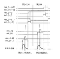
- FIG. 5 is a diagram for explaining a typical driving method by showing the voltage applied to each control line and the output voltage appearing on a vertical signal line in a certain column in the driving method of the present embodiment.
- the (i ⁇ 1) th and (i) th rows are for the row where the reading operation is performed, and the (i + j ⁇ 1) th to the (i + j + 1) th row for the row where the electronic shutter operation is performed.
- the driving period of the i-th row is the (i) scanning period ((i) H), and the driving period of the (i-1) -th row is the (i-1) -th scanning period ((i-1) H). ).
- res_ (i + j) is turned on to start the reset operation of the pixels in the (i + j) th row, and this state is changed to the (i + j + 1) th row in the (i) th scanning period. This is held until after the reset operation of the eye pixel is started. Thereafter, after sel_ (i + j) is turned on, res_ (i + j) is turned off, and sel_ (i + j) is turned off.
- the charge storage unit in the (i + j) th row is not subjected to potential fluctuation due to parasitic capacitance accompanying the start of the reset operation in the (i + j + 1) th row after the reset operation is completed until the start of reading. That is, no afterimage is generated.
- the reset of the pixels in the (i + j ⁇ 1) th row is switched from on to off during the (i ⁇ 1) th scanning period. Further, in FIG. 5, the (i-1) th row is read in the (i-1) th scanning period and the (i) th row is read in the (i) th scanning period by the same method as in FIG.
- the shutter period is j rows, but it is apparent in principle that this functions even if it exceeds the period of one frame.
- Embodiment 3 A solid-state imaging device according to Embodiment 3 of the present invention will be described with reference to FIGS. 6A and 6B.
- the configuration of the solid-state imaging device of this embodiment is the same as that in FIG. 1, and the cross-sectional structure of the pixel portion is the same as that in FIG.
- this is a case of driving for capturing a moving image without using an electronic shutter, that is, a rolling reset operation.
- the driving method shown in FIGS. 3A and 3B in Embodiment Mode 1 is applied in each scanning period, and an operation for sampling the reset signal may be added. It looks like this:
- sel_ (i) is turned on in the (i-1) th scanning period, and the pixel signal in the (i) th row is read. Thereafter, res_ (i) is turned on, and the reset operation of the (i) -th row is started.
- the time from res_ (i + 1) being turned on in the (i) th scanning period until res_ (i) is turned off is arbitrary, and the on / off operation of res_ (i + 1) is arbitrary. However, it must be on immediately before res_ (i) is turned off (exactly, a margin for the reaction time of the storage capacity is required).
- the time at which res_ (i) is turned on in advance is arbitrary (however, it is necessary to consider the reaction time of the charge storage unit or the like).
- sel_ (i) is turned on in the (i ⁇ 1) th scanning period, and the pixel signal in the (i) th row is read out. Thereafter, res_ (i) is turned on, and the reset operation of the (i) -th row is started. After maintaining this state for a time during which the pixel can be reset, res_ (i) is turned off.
- sel_ (i + 1) is turned on, and the pixel signal in the (i + 1) th row is read out. Thereafter, res_ (i + 1) is turned on, and the reset operation is started. After maintaining this state for a time during which the pixel can be reset, res_ (i + 1) is turned off. After that, sel_ (i) and res_ (i) are turned on, and (i) reset of the row is started (the sel_ (i) is not necessarily turned on. However, the transistor gate control line for selection and In order to suppress the influence of the parasitic component with the charge storage unit on the output signal, it is preferable to turn it on).
- res_ (i) is turned off, and the reset operation is terminated.
- the amount of charge in the charge accumulating portion on the (i + 1) th row does not substantially depend on the amount of light irradiation, so that afterimage can be prevented by this driving method according to the principle described in the first embodiment.
- the driving method described in this embodiment does not include reset signal readout.
- Embodiment 4 A solid-state imaging device according to Embodiment 4 of the present invention will be described with reference to FIGS.
- the configuration of the solid-state imaging device of this embodiment is the same as that of FIG. 1, and the cross-sectional structure of the pixel portion is the same as that of FIG.
- FIG. 7 schematically shows the pixel array 502 of the present embodiment, which is equivalent to FIG.
- Pixels in n rows (n is an integer of 2 or more) are arranged in the vertical scanning direction.
- the circuit diagram of each pixel is the same as that in FIG. 14, and the gate of the reset transistor 106 in each row is controlled by one reset control line in each row.
- the gate of the selection transistor 105 is controlled by a selection control line.
- Each row is numbered from 1 to n in the vertical scanning direction, the reset control line of the i-th row (i is an integer not less than 1 and not more than (n ⁇ 1)) is res_ (i), and the selection control line is sel_
- the notation (i) is the same as in FIG.
- signals are read out line by line in the illustrated direction (from bottom to top).
- a column amplifier 904 belonging to the column amplifier circuit 504 and a noise canceller circuit 905 for one column belonging to the noise canceller circuit 905 are shown.
- the noise canceller circuit 905 includes a first correlated double sampling circuit (first CDS circuit) including a switch 906, a capacitor 907, a switch 908, a capacitor 909, and a switch 910, a switch 911, a capacitor 912, a switch 913, and a capacitor 914.
- second CDS circuit comprising a switch 915 is connected in parallel.
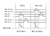
- FIG. 8 is a diagram for explaining a typical driving method by showing the voltage applied to each control line and the output voltage appearing on a vertical signal line in a certain column in the driving method of the present embodiment.
- the i-th drive period is referred to as the (i) th scan period ((i) H)
- the (i + 1) th drive period is referred to as the (i + 1) th scan period ((i + 1) H).
- the second reset operation in the (i) th row is performed. Specifically, the switch 906 is turned on again, sel_ (i) and res_ (i) are turned on, and then turned off in the order of res_ (i) and sel_ (i).
- the vertical output signal V2 at this time is sampled by the first CDS circuit. Thereby, the difference between the previous sampling voltage V1 and this voltage V2 is obtained as the output voltage of the first CDS circuit. Thereafter, the output voltage of the CDS circuit obtained in each column is sequentially output to the outside of the solid-state imaging device by the horizontal driving circuit, and the driving in the (i) scanning period is finished. The same is true after the next (i + 1) th scanning period.
- the output voltage V1 in the next frame is obtained by adding only the voltage corresponding to the light intensity irradiated to each pixel that has no influence of the coupling of the reset operation to the output voltage V2 in the previous frame.
- the voltage (V1-V2) obtained by the CDS circuit is a true image signal that depends only on the light intensity. Therefore, also in the present embodiment, it is possible to capture a high-quality image with no afterimage.
- FIG. 9 is a block diagram showing a configuration of a solid-state imaging apparatus 1101 according to Embodiment 5 of the present invention.
- This solid-state imaging device 1101 includes a pixel array 1102, row signal drive circuits 1103a and 1103b, a column feedback circuit 1104 in which a circuit having an amplification and feedback function is arranged for each column, a column amplifier arranged in each column, A noise canceller circuit 1105 including a noise canceller, a horizontal drive circuit 1106, and an output stage amplifier 1107 are provided.
- the column feedback circuit 1104 receives and feeds back an output signal from the pixel array 1102. Therefore, the direction of signal flow is bidirectional with respect to the pixel array 1102 as shown in FIG.
- FIG. 10 is a circuit diagram showing a signal readout circuit of one pixel 1110 and its peripheral circuit included in the solid-state imaging device 1101.
- the pixel array 1102 includes a plurality of pixels 1110 arranged in a matrix, a plurality of column signal lines (vertical signal lines) 1204 provided for each column, and a plurality of row selection lines provided for each row. including.
- Each of the plurality of column signal lines 1204 is connected to a plurality of pixels 1110 arranged in the corresponding column.
- Each of the plurality of row selection lines is connected to a plurality of pixels 1110 arranged in the corresponding row.
- the pixel 1110 includes a photoelectric conversion unit 1201 and a signal readout circuit.
- the solid-state imaging device 1101 includes a column signal line 1204, a feedback amplifier 1205, a control circuit 1207 that controls an input level to the reset transistor 1206 according to an output from the feedback amplifier 1205, and an amplification transistor 1202.
- a transistor 1203, a column amplifier circuit 1212, a transistor 1210, and capacitors 1213 and 1214 are provided.
- the column signal line 1204, the feedback amplifier 1205, the control circuit 1207, the selection transistor 1203, the column amplification circuit 1212, the transistors 1210 and 1215, and the capacitors 1213 and 1214 are provided for each column.
- the photoelectric conversion unit 1201 generates signal charges corresponding to the amount of incident light by photoelectrically converting incident light.
- the signal read circuit generates a read signal corresponding to the signal charge generated by the photoelectric conversion unit 1201.
- This signal readout circuit includes an amplification transistor 1202, a selection transistor 1203, a reset transistor 1206, and an FD portion (floating diffusion portion) (not shown; the node voltage is described as V FD ).
- the amplification transistor 1202 detects the signal charge amount generated in the photoelectric conversion unit 1201.
- the selection transistor 1203 controls whether the signal detected by the amplification transistor 1202 is transmitted to the column signal line 1204.
- the reset transistor 1206 supplies a reset signal for resetting the photoelectric conversion unit 1201 and the FD unit to the FD unit.
- the control circuit 1207 controls the ON / OFF state of the reset transistor 1206 via the signal line in accordance with the output from the feedback amplifier 1205, and the photoelectric conversion unit controls the input level to the reset transistor 1206 via the signal line.
- 1201 is applied as a ground potential (hereinafter referred to as GND) or a high level potential (hereinafter referred to as V HIGH ).
- the selection transistor 1203 controls whether or not to transmit the pixel output signal V PIXO to the input terminal to the column amplifier circuit 1212.
- the transistor 1215 and the capacitors 1213 and 1214 are connected in series.
- the transistor 1215 controls whether or not the bias voltage V NCB is applied to the capacitor 1213.
- the signal amplified by the column amplifier circuit 1212 is input to a differential circuit including a transistor 1215 and capacitors 1213 and 1214. Then, the difference circuit detects a voltage corresponding to the signal by a difference operation.
- the configuration of the pixel array 1102 is the same as that in Embodiment 2 (FIG. 4).
- FIG. 11 is a diagram for explaining a typical driving method in the driving method according to the present embodiment by showing the voltage applied to each control line and the output voltage appearing on a vertical signal line in a certain column.
- the driving period of the i-th row is the (i) scanning period ((i) H)
- the driving period of the (i-1) -th row is the (i-1) -th scanning period ((i-1) H).
- the description will be made assuming that the noise canceller circuit 1105 has the same configuration as the noise canceller circuit 905.
- sel_ (i) is first turned on, and the selection transistor 1203 in the pixel on the (i) th row is turned on. Then, a voltage V 1 corresponding to the charge accumulated in the FD portion is generated by the amplification transistor 1202 and output to the column signal line 1204. This operation is performed with the switch 906 turned on, and sampling is performed by the first CDS circuit.
- the reset operation of the (i) line is started. Specifically, the switch 906 is turned off, res_ (i) is turned on, and the FD portion is reset by the reset transistor 1206 (a reset voltage is given to the reset transistor 1206 in advance by a voltage source or the like). Thereafter, res_ (i) is turned off to end the first reset operation in the (i) th row. At this time, the output after reset in the (i) th row is not sampled by the second CDS circuit.
- the second reset operation in the (i) th row is performed. Specifically, the switch 906 is turned on again, sel_ (i) and res_ (i) are turned on, and then turned off in the order of res_ (i) and sel_ (i).
- the vertical output signal V2 at this time is sampled by the first CDS circuit. Thereby, the difference between the previous sampling voltage V1 and this voltage V2 is obtained as the output voltage of the first CDS circuit. Thereafter, the output voltage of the CDS circuit obtained in each column is sequentially output to the outside of the solid-state imaging device by the horizontal driving circuit, and the driving in the (i) scanning period is finished. The same is true after the next (i + 1) th scanning period.
- the output voltage V1 in the next frame is obtained by adding only the voltage corresponding to the light intensity irradiated to each pixel that has no influence of the coupling of the reset operation to the output voltage V2 in the previous frame.
- the voltage (V1-V2) obtained by the CDS circuit is a true image signal that depends only on the light intensity. Therefore, also in the present embodiment, it is possible to capture a high-quality image with no afterimage.
- the reset operation is performed with the output fed back via the feedback amplifier 1205. With such a configuration, the inversion of the noise appearing at the output is fed back to the input, added with the positive sign component, and canceled.
- the reset signal is tapered at the end of the second reset in the (i) th row, so that a rapid reset operation is not performed.
- a rapid reset operation is not performed.
- This taper reset operation is not necessary in the present embodiment at the time of the first reset.
- the taper reset operation is performed. The higher noise reduction effect can be obtained.
- Embodiment 6 A solid-state imaging device driving method according to Embodiment 5 of the present invention will be described with reference to FIGS.
- the configuration of the solid-state imaging device of this embodiment is the same as that of FIG. 1, and the cross-sectional structure of the pixel portion is the same as that of FIG.
- FIG. 12 schematically shows the pixel array 502 of this embodiment, which is equivalent to FIG. Pixels in (2k) rows (2k and n are equal) are arranged in the vertical scanning direction.
- Pixels in (2k) rows (2k and n are equal) are arranged in the vertical scanning direction.
- it can be expressed as (2k + 1) rows.
- a is an integer of 0 to k.
- FIG. 13 is a diagram showing a driving method in the present embodiment.
- FIG. 13 shows so-called interlaced driving.
- An odd row signal is read in an odd frame and an even row signal is read in an even frame (the reverse combination is of course possible).
- the pixel signal of the (2a + 1) th row is read during the (a) scanning period.
- sel_ (2a + 1) is turned on, a voltage corresponding to the accumulated charge amount is read out to the vertical signal line, and is sampled by a CDS circuit or the like.
- res_ (2a + 1) is turned on to start the reset operation.
- the reset signal is read from the vertical signal line and sampled by a CDS circuit or the like.
- res_ (2a) is turned on, and the reset operation for the row (2a) is started.
- res_ (2a) is turned off and the reset operation is terminated.
- the reset operation of the (2a + 1) -th row since the reset operation of the (2a + 1) -th row has been completed and less than one scanning period has elapsed, the reset operation of the (2a) -th row hardly affects the light irradiation amount of the (2a + 1) -th row. Afterimages can be prevented.
- sel_ (2a) may be on or off (it is on in FIG. 13), but to the output signal of the parasitic component of the selection transistor gate control line and the storage capacitor. It is better to turn on to suppress the influence of.
- the (2a + 1) th row in the (a) scanning period in the odd frame described above is the (2a) row and the (2a) row is the (2a-1) row, respectively. Replace. With this operation, it is possible to secure an accumulation time of one frame and prevent afterimages.
- the present invention is not limited to these embodiments. Unless it deviates from the meaning of this invention, the form which carried out the various deformation
- the present invention is effective for digital still cameras, digital video cameras, and the like.
Landscapes
- Engineering & Computer Science (AREA)
- Multimedia (AREA)
- Signal Processing (AREA)
- Transforming Light Signals Into Electric Signals (AREA)
- Solid State Image Pick-Up Elements (AREA)
Abstract
The purpose of the present invention is to provide a method for driving a solid-state imaging device capable of capturing a high-quality image without the occurrence of a residual image phenomenon even when capturing a moving image with a steep change in brightness. The solid-state imaging device includes pixels arranged in a two dimensional matrix having m columns in a horizontal scanning direction and n rows in a vertical scanning direction, where n is an integer of 2 or more and m is a natural number. When a reset operation for the pixels in the i-th row (where i is an integer of 1 to n-1, inclusive) is completed, the reset operation for the pixels in the (i+1)-th row is in progress or the elapsed time from the completion of the reset operation for the pixels in the (i+1)-th row is less than one-frame imaging time.
Description
本発明は、画像を電気信号として出力する固体撮像装置の駆動方法に関する。
The present invention relates to a method for driving a solid-state imaging device that outputs an image as an electrical signal.
CMOS(Complementary Metal Oxide Secmiconductor)及びMOS(Metal Oxide Secmiconductor)エリアイメージセンサ(以下両者を併せてCMOS固体撮像装置と称する)、並びに電荷結合素子(Charge Coupled Devices)エリアイメージセンサ(以下CCD固体撮像装置と称する)は、入力光情報を光電変換することにより画像信号を生成する。これらの固体撮像装置は、機能素子として、デジタルスチルカメラ、デジタルビデオカメラ、ネットワークカメラ、及び携帯電話用カメラ等、多岐にわたる撮像機器に用いられている。
CMOS (Complementary Metal Oxide Semiconductor) and MOS (Metal Oxide Semiconductor) area image sensors (hereinafter collectively referred to as CMOS solid-state imaging devices), and charge-coupled device (Charge Coupled Devices) CCD image sensor (hereinafter referred to as “Charge Coupled Devices”). The image signal is generated by photoelectrically converting the input light information. These solid-state imaging devices are used as functional elements in a wide variety of imaging devices such as digital still cameras, digital video cameras, network cameras, and mobile phone cameras.
従来の固体撮像装置は、半導体基板の最表面に、光電変換部(フォトダイオード)と読み出し回路部とを有する画素を二次元のアレイ状に配置した構成を有する。したがって、光電変換部の面積は光入射面において読み出し回路部の面積分削減される。これにより、従来の固体撮像装置では、開口率が低下するという課題があった。
A conventional solid-state imaging device has a configuration in which pixels having a photoelectric conversion unit (photodiode) and a readout circuit unit are arranged in a two-dimensional array on the outermost surface of a semiconductor substrate. Therefore, the area of the photoelectric conversion unit is reduced by the area of the readout circuit unit on the light incident surface. As a result, the conventional solid-state imaging device has a problem that the aperture ratio decreases.
この課題を解決するために、光吸収能を有する材料を基板上に積層した構成の光電変換部と、基板に形成した読出し回路とを有する積層型固体撮像装置が特許文献1及び特許文献2に報告されている。
In order to solve this problem, Patent Document 1 and Patent Document 2 disclose stacked solid-state imaging devices each including a photoelectric conversion unit having a structure in which a light-absorbing material is stacked on a substrate and a readout circuit formed on the substrate. It has been reported.
これらの文献に記載の積層型固体撮像装置では、各画素の光電変換部は、画素電極と、その上方(光入射側)に積層された光電変換膜と、その上面に形成された対向電極とを含む。さらに、当該積層型固体撮像装置は、入射光によって発生した電荷群を電流信号として画素電極を介して光電変換部外に取り出す。当該積層型固体撮像装置は、通常、信号電荷の符号を選択するために信号電荷を伝導し、その反対符号の電荷をブロックする電荷ブロッキング層を備える。当該電荷ブロッキング層は、画素電極に対向する、又は画素電極に直接接している。
In the stacked solid-state imaging device described in these documents, the photoelectric conversion unit of each pixel includes a pixel electrode, a photoelectric conversion film stacked above (light incident side), and a counter electrode formed on the upper surface thereof. including. Further, the multilayer solid-state imaging device takes out a charge group generated by incident light as a current signal outside the photoelectric conversion unit via the pixel electrode. The stacked solid-state imaging device usually includes a charge blocking layer that conducts signal charges to select a sign of signal charges and blocks charges of opposite signs. The charge blocking layer faces the pixel electrode or is in direct contact with the pixel electrode.
図14は、特許文献1に記載されている有機膜を光電変換膜とする従来の積層型イメージセンサの画素部(画素)の回路を模式的に示したものである。光電変換部101から画素電極102を通して出力された信号電荷は、基板上に形成された空乏層容量よりなる電荷蓄積部103に蓄積される。当該電荷蓄積部103は配線を介して画素読み出しトランジスタ(増幅トランジスタ)104の入力ゲートに接続され、蓄積電荷量の変動に伴う電圧変化が検出され、当該画素の読み出しタイミングを選択する選択トランジスタ105を介して読み出し信号として垂直信号線107に出力される。さらに信号電荷が読み出された後に、当該電荷蓄積部103の電荷をリセットするためにリセットトランジスタ106のドレイン部が電荷蓄積部103に接続されており、リセット時に初期状態電圧に電荷蓄積部電圧が設定される。
FIG. 14 schematically shows a circuit of a pixel portion (pixel) of a conventional stacked image sensor using an organic film described in Patent Document 1 as a photoelectric conversion film. The signal charge output from the photoelectric conversion unit 101 through the pixel electrode 102 is stored in the charge storage unit 103 formed of a depletion layer capacitance formed on the substrate. The charge storage unit 103 is connected to an input gate of a pixel readout transistor (amplification transistor) 104 via a wiring, and a selection transistor 105 that detects a change in voltage associated with a change in the amount of stored charge and selects a readout timing of the pixel. Through the vertical signal line 107 as a readout signal. Further, after the signal charge is read, the drain part of the reset transistor 106 is connected to the charge storage part 103 in order to reset the charge of the charge storage part 103, and the charge storage part voltage is set to the initial state voltage at the time of reset. Is set.
図15は図14の画素を二次元状に配列した積層型固体撮像装置を模式的に示したものであり、垂直走査方向にn行(nは2以上の整数とする)の画素が配列されている。各行のリセットトランジスタ106のゲートは各行それぞれ一本のリセット制御線で制御される。同様に、選択トランジスタ105のゲートは選択制御線で制御される。各行を垂直走査方向に1からnまで番号付けすることとし、i行目(iは1以上(n-1)以下の整数とする)のリセット制御線をres_(i)、選択制御線をsel_(i)と記し、積層型固体撮像装置の典型的な動画撮影時の駆動方法を図16によって説明する。
FIG. 15 schematically shows a stacked solid-state imaging device in which the pixels of FIG. 14 are two-dimensionally arranged, and n rows (n is an integer of 2 or more) of pixels are arranged in the vertical scanning direction. ing. The gates of the reset transistors 106 in each row are controlled by one reset control line for each row. Similarly, the gate of the selection transistor 105 is controlled by a selection control line. Each row is numbered from 1 to n in the vertical scanning direction, the reset control line of the i-th row (i is an integer not less than 1 and not more than (n−1)) is res_ (i), and the selection control line is sel_ (I) and a typical driving method of the multilayer solid-state imaging device at the time of moving image shooting will be described with reference to FIG.
図16は、各制御線に与える電圧および、ある列の垂直信号線107に現れる出力電圧を示すことで、典型的な駆動方法を説明する図である。図16では第(i-1)行から第(i+1)行しか記載していないが、第1行から第n行まで同様の駆動を順番に行えば一画面分の画像信号が得られることは当業者ならば容易に理解できるので省略している。また、i行目の駆動期間(水平走査期間)を第(i)走査期間と記している。
FIG. 16 is a diagram for explaining a typical driving method by showing a voltage applied to each control line and an output voltage appearing on a vertical signal line 107 in a certain column. In FIG. 16, only the (i−1) th to (i + 1) th rows are shown, but if the same driving is sequentially performed from the first to nth rows, an image signal for one screen can be obtained. Since it can be easily understood by those skilled in the art, it is omitted. In addition, the driving period (horizontal scanning period) of the i-th row is described as the (i) th scanning period.
第(i-1)走査期間では、まずsel_(i-1)をオンして、第(i-1)行目の画素内の選択トランジスタ105をオンする。すると、電荷蓄積部103に蓄積された電荷に対応する電圧V1が画素読み出しトランジスタ104により生成され、垂直信号線107に出力される(この電圧V1を画素信号と記す)。これは後段の相関二重サンプリング(CDS)回路などによってサンプリングされる。(以下、この動作を「画素信号の読み出し」と呼ぶ)。次に(i-1)行目のリセット動作を開始する。具体的には、res_(i-1)をオンし、リセットトランジスタ106により電荷蓄積部103をリセットする(リセットトランジスタ106には電圧源などによりリセット電圧をあらかじめあたえておく)。そのあとres_(i-1)をオフすることで(i-1)行目のリセット動作を終了し、垂直信号線107に出力される電圧V2(これをリセット信号と記す)をCDS回路などでサンプリングする(この動作を以下では「リセット信号の読出し」と呼ぶ)。これにより、先ほどのサンプリング電圧V1とこの電圧V2との差がCDS回路の出力電圧として得られる。そのあと、各列で得られるCDS回路の出力電圧を、水平転送回路により順番に固体撮像装置外に出力し、第(i-1)走査期間の駆動を終える。次の第(i)走査期間以下でも同様の駆動が行われる。第(n)走査期間が終われば、次のフレームの第(1)走査期間から同様の駆動が繰り返される。次のフレームでの出力電圧V1は、前のフレームの出力電圧V2に、各画素へ照射される光強度に対応した電圧が加算されたものになるので、CDS回路により得られる電圧(V1-V2)は、光強度のみに依存した真の画像信号ということになる。
In the (i-1) th scanning period, first, sel_ (i-1) is turned on, and the selection transistor 105 in the pixel on the (i-1) th row is turned on. Then, a voltage V1 corresponding to the charge accumulated in the charge accumulation unit 103 is generated by the pixel readout transistor 104 and output to the vertical signal line 107 (this voltage V1 is referred to as a pixel signal). This is sampled by a subsequent correlated double sampling (CDS) circuit or the like. (Hereinafter, this operation is referred to as “pixel signal readout”). Next, the reset operation of the (i-1) th row is started. Specifically, res_ (i−1) is turned on, and the charge accumulation unit 103 is reset by the reset transistor 106 (a reset voltage is given to the reset transistor 106 in advance by a voltage source or the like). Thereafter, res_ (i-1) is turned off to complete the reset operation of the (i-1) th row, and the voltage V2 (referred to as a reset signal) output to the vertical signal line 107 is output by a CDS circuit or the like. Sampling is performed (this operation is hereinafter referred to as “reset signal reading”). Thereby, the difference between the sampling voltage V1 and the voltage V2 is obtained as the output voltage of the CDS circuit. Thereafter, the output voltage of the CDS circuit obtained in each column is sequentially output to the outside of the solid-state imaging device by the horizontal transfer circuit, and the driving in the (i-1) th scanning period is finished. The same driving is performed even after the next (i) scanning period. When the (n) th scanning period ends, the same driving is repeated from the (1) th scanning period of the next frame. The output voltage V1 in the next frame is obtained by adding the voltage corresponding to the light intensity irradiated to each pixel to the output voltage V2 in the previous frame, and thus the voltage (V1-V2) obtained by the CDS circuit. ) Is a true image signal depending only on the light intensity.
しかしながら、このような駆動方法では、特に輝度が大きく変化する動画撮影時において、前フレームの画像が次フレームに現れる、いわゆる残像が生じるという課題があることが本願発明者らの研究によって明らかとなった。以下にその詳細を説明する。
However, such a driving method has a problem that a so-called afterimage is generated, in which an image of the previous frame appears in the next frame, particularly during moving image shooting in which the luminance changes greatly. It was. Details will be described below.
図17は垂直走査方向に隣接するi行目と(i+1)行目の2つの画素を示す図であり、各画素の構成は図14と同様である。ただし、図17では、これらの画素間の寄生容量108を追加している。寄生容量108は画素電極102間、画素読み出しトランジスタ104のゲート配線間などで生じる。電荷蓄積部(蓄積容量)103の値をCa(これは通常全画素で同じ値である)、寄生容量108の値をCpとする。
FIG. 17 is a diagram showing two pixels in the i-th row and the (i + 1) -th row adjacent in the vertical scanning direction, and the configuration of each pixel is the same as that in FIG. However, in FIG. 17, a parasitic capacitance 108 between these pixels is added. The parasitic capacitance 108 is generated between the pixel electrodes 102, between the gate wirings of the pixel readout transistor 104, and the like. The value of the charge storage unit (storage capacitor) 103 is Ca (this is usually the same value for all pixels), and the value of the parasitic capacitor 108 is Cp.
この寄生容量108により、以下のようなメカニズムで残像が発生する。
Due to this parasitic capacitance 108, an afterimage is generated by the following mechanism.
図16の第(i)走査期間において、(i)行目のリセット動作終了後すなわち、res_(i)をオフした直後の蓄積容量103(i)の電圧をVres(i)とする。またこのときの蓄積容量103(i+1)の電圧をVfd1(i+1)とする。Vres1(i)はリセットトランジスタ106(i)に与えられるリセット電圧、リセットトランジスタ106(i)の閾値や(蓄積容量103側をドレインとすると)ゲート・ドレイン間容量によって決定され、画素に照射される光強度には依らない。それに対し、Vfd1(i+1)は、(i+1)行目の画素に照射された光強度に依存する。
In the (i) scanning period of FIG. 16, the voltage of the storage capacitor 103 (i) after the reset operation of the (i) th row is completed, that is, immediately after res_ (i) is turned off, is Vres (i). In addition, the voltage of the storage capacitor 103 (i + 1) at this time is set to Vfd1 (i + 1). Vres1 (i) is determined by the reset voltage applied to the reset transistor 106 (i), the threshold value of the reset transistor 106 (i), and the gate-drain capacitance (assuming the storage capacitor 103 side is the drain), and is applied to the pixel. It does not depend on the light intensity. On the other hand, Vfd1 (i + 1) depends on the light intensity applied to the pixels in the (i + 1) th row.
この後、第(i+1)走査期間において、(i+1)行目のリセット動作終了後すなわち、res_(i+1)をオフした直後では、蓄積容量103(i+1)の電圧がVres1(i+1)に変化する。このとき蓄積容量103(i)は何ら電圧源に接続されておらず、いわゆるフローティングであるから、蓄積容量103(i+1)の電圧変化が蓄積容量103(i)の電圧に影響を及ぼす。すなわち、蓄積容量103(i)のこの瞬間での電圧をVres2(i)とすると、
Thereafter, in the (i + 1) th scanning period, after the reset operation of the (i + 1) th row is completed, that is, immediately after res_ (i + 1) is turned off, the voltage of the storage capacitor 103 (i + 1) changes to Vres1 (i + 1). At this time, since the storage capacitor 103 (i) is not connected to any voltage source and is so-called floating, a voltage change of the storage capacitor 103 (i + 1) affects the voltage of the storage capacitor 103 (i). That is, if the voltage at this moment of the storage capacitor 103 (i) is Vres2 (i),

この後、次のフレームの第(i)走査期間まで(i)行目の画素に光が照射され、電荷が蓄積される。この電荷をQaとする。
Thereafter, the pixels in the (i) th row are irradiated with light until the (i) scanning period of the next frame, and electric charges are accumulated. This charge is Qa.
次のフレームの第(i)走査期間において、選択トランジスタ105(i)をオンしたときの蓄積容量103(i)の電圧は、上記QaとVres2(i)を加算した値に略等しいので、この電圧値をVout(i)とすると、
In the (i) scanning period of the next frame, the voltage of the storage capacitor 103 (i) when the selection transistor 105 (i) is turned on is substantially equal to the sum of Qa and Vres2 (i). When the voltage value is Vout (i),

本発明は、上記従来技術の実情に鑑みてなされたものであり、輝度変化の激しい動画撮像時においても、残像現象の発生しない高画質撮像を可能とする固体撮像装置の駆動方法を提供することを目的とする。
The present invention has been made in view of the above-described prior art, and provides a driving method of a solid-state imaging device that enables high-quality imaging without occurrence of an afterimage phenomenon even when capturing moving images with a sharp change in luminance. With the goal.
上記従来技術の課題を解決するために、本発明の一形態に係る固体撮像装置の駆動方法は、水平走査方向にm列、垂直走査方向にn行の2次元状に配列された画素を含む固体撮像装置の駆動方法であって(nは2以上の整数、mは自然数とする)、i行目(iは1以上n-1以下の整数とする)の前記画素のリセット動作を終了するとき、(i+1)行目の前記画素がリセット動作中であるか、もしくは(i+1)行目の前記画素がリセット動作を終了してからの経過時間が1フレーム撮像時間未満であることを特徴とする。このような駆動方法とすることによって、所定の行のリセット動作終了後には、所定の行に隣接する行のリセット動作のカップリングによる出力信号の電位変動が発生しない。従って、フレーム間で残像は全く発生しない。
In order to solve the above-described problems of the related art, a driving method of a solid-state imaging device according to an aspect of the present invention includes pixels arranged in a two-dimensional array of m columns in the horizontal scanning direction and n rows in the vertical scanning direction. This is a driving method of the solid-state imaging device (n is an integer of 2 or more, m is a natural number), and the reset operation of the pixel in the i-th row (i is an integer of 1 to n-1) is completed. The pixel in the (i + 1) th row is being reset, or the elapsed time after the pixel in the (i + 1) th row has finished the reset operation is less than one frame imaging time. To do. By adopting such a driving method, after the reset operation of a predetermined row is finished, the potential fluctuation of the output signal due to coupling of the reset operation of the row adjacent to the predetermined row does not occur. Therefore, no afterimage occurs between frames.
さらに上記従来技術の課題を解決するために、本発明の一形態に係る固体撮像装置の駆動方法は、j水平走査期間(jは1以上(n-1)以下の整数とする)の蓄積時間を与える電子シャッタの駆動を行い、i行目の前記画素からの画素信号を読み出す走査期間中に、(i+j)行目の前記画素のリセット動作を終了する前に、(i+j+1)行目の前記画素のリセット動作を開始することを特徴とする。読み出し行のリセット動作終了後には、隣接する行のリセット動作のカップリングによる出力信号の電位変動が発生しない。従って、フレーム間で残像は発生しない。
Further, in order to solve the above-described problems of the related art, the driving method of the solid-state imaging device according to one aspect of the present invention includes an accumulation time of j horizontal scanning periods (j is an integer of 1 to (n−1)). Before the reset operation of the pixel in the (i + j) row is completed during the scanning period for reading out the pixel signal from the pixel in the i row. The pixel reset operation is started. After the reset operation of the read row is completed, the potential fluctuation of the output signal due to the coupling of the reset operation of the adjacent row does not occur. Therefore, no afterimage occurs between frames.
さらに上記従来技術の課題を解決するために、本発明の一形態に係る固体撮像装置の駆動方法は、(i+1)行目(iは1以上n-1以下の整数とする)の画素信号読出し動作と、(i+1)行目のリセット動作の開始と、i行目のリセット動作の終了とを順次行うことを特徴とする。このような駆動方法とすることによって、隣接する行のリセット動作のカップリングによる出力信号の電位変動は、2度目のリセット動作で除去できるので、フレーム間で残像は発生しない。
Further, in order to solve the above-described problems of the related art, the driving method of the solid-state imaging device according to one aspect of the present invention is to read out pixel signals of the (i + 1) -th row (i is an integer of 1 to n-1). The operation, the start of the reset operation of the (i + 1) -th row, and the end of the reset operation of the i-th row are sequentially performed. By adopting such a driving method, the potential fluctuation of the output signal due to the coupling of the reset operation of the adjacent row can be removed by the second reset operation, so that no afterimage is generated between frames.
さらに上記従来技術の課題を解決するために、本発明の一形態に係る固体撮像装置の駆動方法は、(i+1)行目(iは1以上n-1以下の整数とする)の画素信号読出し動作と、(i+1)行目のリセット動作の開始と、(i+1)行目のリセット動作の終了と、(i+1)行目のリセット信号読出し動作と、i行目のリセット動作の終了とを順次行うことを特徴とする。このような駆動方法とすることによって、隣接する行のリセット動作のカップリングによる出力信号の電位変動は、2度目のリセット動作で除去できるので、フレーム間で残像は発生しない。
Further, in order to solve the above-described problems of the related art, the driving method of the solid-state imaging device according to one aspect of the present invention is to read out pixel signals of the (i + 1) -th row (i is an integer of 1 to n-1). The operation, the start of the reset operation of the (i + 1) th row, the end of the reset operation of the (i + 1) th row, the reset signal reading operation of the (i + 1) th row, and the end of the reset operation of the ith row are sequentially performed. It is characterized by performing. By adopting such a driving method, the potential fluctuation of the output signal due to the coupling of the reset operation of the adjacent row can be removed by the second reset operation, so that no afterimage is generated between frames.
さらに上記従来技術の課題を解決するために、本発明の一形態に係る固体撮像装置の駆動方法は、(i+1)行目(iは1以上n-1以下の整数とする)の画素信号読出し動作と、(i+1)行目のリセット動作の開始と、i行目のリセット動作の終了と、i行目のリセット信号読出し動作とを順次行うことを特徴とする。このような駆動方法とすることによって、隣接する行のリセット動作のカップリングによる出力信号の電位変動は、2度目のリセット動作で除去できるので、フレーム間で残像は発生しない。
Further, in order to solve the above-described problems of the related art, the driving method of the solid-state imaging device according to one aspect of the present invention is to read out pixel signals of the (i + 1) -th row (i is an integer of 1 to n-1). The operation, the start of the reset operation of the (i + 1) th row, the end of the reset operation of the i row, and the reset signal read operation of the i row are sequentially performed. By adopting such a driving method, the potential fluctuation of the output signal due to the coupling of the reset operation of the adjacent row can be removed by the second reset operation, so that no afterimage is generated between frames.
さらに上記従来技術の課題を解決するために、本発明の一形態に係る固体撮像装置の駆動方法は、水平走査方向にm列、垂直走査方向に2k行又は(2k+1)行の2次元状に配列された画素を含む固体撮像装置において(2kとnとが等しい、又は(2k+1)とnとが等しい)、(2a+1)行目(aは0以上k以下の整数とする)の画素信号読出し動作と、(2a+1)行目のリセット動作と、(2a+1)行目のリセット信号読出し動作と、2a行目のリセット動作とを順次行う奇数フレームの駆動と、(2a+2)行目の画素信号読出し動作と、(2a+2)行目のリセット動作と、(2a+2)行目のリセット信号読出し動作と、(2a+1)行目のリセット動作とを順次行う偶数フレームの駆動とを含むことを特徴とする。このような駆動方法とすることによって、読み出し行のリセット動作終了後には、隣接する行のリセット動作のカップリングによる出力信号の電位変動が発生しない。従って、フレーム間で残像は発生しない。
Further, in order to solve the above-described problems of the prior art, a driving method of a solid-state imaging device according to an aspect of the present invention is a two-dimensional form of m columns in the horizontal scanning direction and 2k rows or (2k + 1) rows in the vertical scanning direction. In a solid-state imaging device including arranged pixels (2k and n are equal, or (2k + 1) and n are equal), (2a + 1) -th pixel signal (a is an integer of 0 to k) Operation, driving of the odd-numbered frame in which the reset operation of the (2a + 1) th row, the reset signal reading operation of the (2a + 1) th row, and the reset operation of the 2a row are sequentially performed, and the pixel signal reading of the (2a + 2) th row And an even-numbered frame driving in which the reset operation of the (2a + 2) th row, the reset signal reading operation of the (2a + 2) th row, and the reset operation of the (2a + 1) th row are sequentially performed. With such a driving method, after the reset operation of the readout row is finished, the potential fluctuation of the output signal due to the coupling of the reset operation of the adjacent row does not occur. Therefore, no afterimage occurs between frames.
以上のように、輝度変化の激しい動画撮像時においても、行読み出し後の隣接行のリセット動作のカップリングによって発生する出力変動を除去し、フレーム間残像の発生しない高画質撮像を可能とする固体撮像装置の駆動方法を提供できる。
As described above, even when capturing moving images with significant changes in luminance, a solid state that eliminates output fluctuations caused by coupling of the reset operation of adjacent rows after row readout and enables high-quality imaging that does not cause interframe afterimages. A driving method of the imaging apparatus can be provided.
以下、本発明に係る固体撮像装置の駆動方法の実施の形態について、図面を参照しながら説明する。なお、本発明について、以下の実施の形態及び添付の図面を用いて説明を行うが、これは例示を目的としており、本発明がこれらに限定されることを意図しない。以下の実施の形態で示される数値、形状、材料、構成要素、構成要素の配置位置及び接続形態、ステップ、ステップの順序などは、一例であり、本発明を限定する主旨ではない。また、以下の実施の形態における構成要素のうち、本発明の最上位概念を示す独立請求項に記載されていない構成要素については、より好ましい形態を構成する任意の構成要素として説明される。
Hereinafter, embodiments of a method for driving a solid-state imaging device according to the present invention will be described with reference to the drawings. In addition, although this invention is demonstrated using the following embodiment and attached drawing, this is for the purpose of illustration and this invention is not intended to be limited to these. The numerical values, shapes, materials, constituent elements, arrangement positions and connecting forms of the constituent elements, steps, order of steps, and the like shown in the following embodiments are merely examples, and are not intended to limit the present invention. In addition, among the constituent elements in the following embodiments, constituent elements that are not described in the independent claims indicating the highest concept of the present invention are described as optional constituent elements that constitute a more preferable embodiment.
(実施の形態1)
本発明の実施の形態1に係る固体撮像装置の駆動方法について図1から図3Bを用いて説明する。 (Embodiment 1)
A method for driving the solid-state imaging device according toEmbodiment 1 of the present invention will be described with reference to FIGS. 1 to 3B.
本発明の実施の形態1に係る固体撮像装置の駆動方法について図1から図3Bを用いて説明する。 (Embodiment 1)
A method for driving the solid-state imaging device according to
まず、本発明の実施の形態1に係る固体撮像装置の全体構成を説明する。図1は、本発明の実施の形態1に係る固体撮像装置501の構成を示すブロック図である。
First, the overall configuration of the solid-state imaging device according to Embodiment 1 of the present invention will be described. FIG. 1 is a block diagram showing a configuration of a solid-state imaging device 501 according to Embodiment 1 of the present invention.
この固体撮像装置501は、画素アレイ502と、行信号駆動回路503a及び503bと、列毎に配置された列アンプ回路504と、各列に配置されたノイズキャンセラ回路505と、水平駆動回路506と、出力段アンプ507とを備える。
The solid-state imaging device 501 includes a pixel array 502, row signal driving circuits 503a and 503b, a column amplifier circuit 504 arranged for each column, a noise canceller circuit 505 arranged for each column, a horizontal driving circuit 506, And an output stage amplifier 507.
図2は、固体撮像装置501の3画素分の領域の断面図である。なお、実際の画素は、画素アレイ502に、例えば1000万画素分配列されている。各画素の回路図は図15と同様である。
FIG. 2 is a cross-sectional view of an area corresponding to three pixels of the solid-state imaging device 501. The actual pixels are arranged in the pixel array 502, for example, for 10 million pixels. The circuit diagram of each pixel is the same as FIG.
図2に示すように、固体撮像装置501は、マイクロレンズ601と、赤色カラーフィルタ602と、緑色カラーフィルタ603と、青色カラーフィルタ604と、保護膜605と、平坦化膜606と、上部電極607(第2電極)と、光電変換膜608と、電子ブロッキング層609と、電極間絶縁膜610と、下部電極611(第1電極)と、配線間絶縁膜612と、給電層613と、配線層614と、基板618と、ウェル619と、STI領域(シャロウトレンチ分離領域)620と、層間絶縁層621とを備える。
As shown in FIG. 2, the solid-state imaging device 501 includes a microlens 601, a red color filter 602, a green color filter 603, a blue color filter 604, a protective film 605, a planarization film 606, and an upper electrode 607. (Second electrode), photoelectric conversion film 608, electron blocking layer 609, interelectrode insulating film 610, lower electrode 611 (first electrode), interwiring insulating film 612, feeding layer 613, wiring layer 614, a substrate 618, a well 619, an STI region (shallow trench isolation region) 620, and an interlayer insulating layer 621.
基板618は、半導体基板であり、例えばシリコン基板である。基板618内には、光電変換膜608の光電変換により生成された信号電荷を信号電圧(読み出し信号)として画素外部に読み出すための信号読み出し回路、つまり複数のトランジスタ(増幅トランジスタ616、選択トランジスタ及びリセットトランジスタ617)が形成されている。
The substrate 618 is a semiconductor substrate, for example, a silicon substrate. In the substrate 618, a signal readout circuit for reading out signal charges generated by photoelectric conversion of the photoelectric conversion film 608 to the outside of the pixel as a signal voltage (readout signal), that is, a plurality of transistors (amplification transistor 616, selection transistor, and reset) Transistor 617) is formed.
マイクロレンズ601は、入射光を効率よく集光するために、固体撮像装置501の最表面に、画素510ごとに形成されている。
The micro lens 601 is formed for each pixel 510 on the outermost surface of the solid-state imaging device 501 in order to efficiently collect incident light.
赤色カラーフィルタ602、緑色カラーフィルタ603及び青色カラーフィルタ604は、カラー画像を撮像するために形成されている。また、赤色カラーフィルタ602、緑色カラーフィルタ603及び青色カラーフィルタ604は、各マイクロレンズ601の直下、かつ保護膜605内に形成されている。1000万画素分にわたって集光ムラ及び色ムラのないマイクロレンズ601及びカラーフィルタ群を形成するために、これらの光学素子は平坦化膜606上に形成されている。平坦化膜606は、例えば、SiNで構成される。
The red color filter 602, the green color filter 603, and the blue color filter 604 are formed for capturing a color image. Further, the red color filter 602, the green color filter 603, and the blue color filter 604 are formed immediately below each microlens 601 and in the protective film 605. These optical elements are formed on the planarizing film 606 in order to form a microlens 601 and a color filter group free from unevenness of color collection and color over 10 million pixels. The planarizing film 606 is made of SiN, for example.
上部電極607は、平坦化膜606下に画素アレイ502の全面にわたって形成されている。この上部電極607は可視光を透過する。例えば、上部電極607はITO(Indium Tin Oxide)で構成される。
The upper electrode 607 is formed under the planarizing film 606 over the entire surface of the pixel array 502. The upper electrode 607 transmits visible light. For example, the upper electrode 607 is made of ITO (Indium Tin Oxide).
光電変換膜608は光を信号電荷に変換する。具体的には、光電変換膜608は、上部電極607の下に形成されており、高い光吸収能を有する有機分子で構成されている。また、光電変換膜608の厚さは、例えば500nmである。また、光電変換膜608は、真空蒸着法を用いて形成される。上記有機分子は波長400nmから700nmの可視光全域にわたって高い光吸収能を有する。
The photoelectric conversion film 608 converts light into signal charges. Specifically, the photoelectric conversion film 608 is formed under the upper electrode 607 and is composed of organic molecules having high light absorption ability. Moreover, the thickness of the photoelectric conversion film 608 is, for example, 500 nm. Further, the photoelectric conversion film 608 is formed by using a vacuum evaporation method. The organic molecule has a high light absorption ability over the entire visible light having a wavelength of 400 nm to 700 nm.
電子ブロッキング層609は、光電変換膜608の下に形成されており、入射光の光電変換によって発生した正孔を伝導するとともに、下部電極611からの電子注入を阻止する。この電子ブロッキング層609は、高い平坦度を有する電極間絶縁膜610と下部電極611上に形成されている。
The electron blocking layer 609 is formed under the photoelectric conversion film 608 and conducts holes generated by photoelectric conversion of incident light and blocks injection of electrons from the lower electrode 611. The electron blocking layer 609 is formed on the interelectrode insulating film 610 and the lower electrode 611 having high flatness.
複数の下部電極611は、基板618の上方に、行列状に配置されている。また、複数の下部電極611は、各々が電気的に分離されている。具体的には、下部電極611は、電極間絶縁膜610間に形成されており、光電変換膜608で発生した正孔を収集する。この下部電極611は、例えばTiNで構成される。また、下部電極611は、平坦化された厚さ100nmの配線間絶縁膜612上に形成されている。
The plurality of lower electrodes 611 are arranged in a matrix above the substrate 618. The plurality of lower electrodes 611 are electrically isolated from each other. Specifically, the lower electrode 611 is formed between the interelectrode insulating films 610 and collects holes generated in the photoelectric conversion film 608. The lower electrode 611 is made of, for example, TiN. The lower electrode 611 is formed on the planarized inter-wiring insulating film 612 having a thickness of 100 nm.
また、各下部電極611は0.2μmの間隔で分離されている。そして、この分離領域にも電極間絶縁膜610が埋め込まれている。
Also, the lower electrodes 611 are separated by an interval of 0.2 μm. An interelectrode insulating film 610 is also embedded in this isolation region.
さらに、この分離領域の下方、かつ配線間絶縁膜612下に給電層613が配されている。この給電層613は、例えばCuで構成される。具体的には、給電層613は、隣接する下部電極611の間の領域であり、かつ下部電極611と基板618との間に形成されている。また、給電層613には、下部電極611とは独立した電位を供給可能である。具体的には、光電変換膜608が光電変換を行う露光動作時、及び信号読み出し回路が読み出し信号を生成する読み出し動作時に、給電層613に、信号電荷を排斥するための電位が供給される。例えば、信号電荷が正孔の場合には正電圧が印加される。これにより、各画素に、隣接画素から正孔が混入することを防止できる。なお、このような電圧印加の制御は、例えば、固体撮像装置501が備える制御部(図示せず)により行なわれる。
Furthermore, a power feeding layer 613 is disposed below the isolation region and below the inter-wiring insulating film 612. The power supply layer 613 is made of Cu, for example. Specifically, the power feeding layer 613 is a region between the adjacent lower electrodes 611 and is formed between the lower electrode 611 and the substrate 618. In addition, a potential independent of the lower electrode 611 can be supplied to the power feeding layer 613. Specifically, a potential for discharging signal charges is supplied to the power supply layer 613 during an exposure operation in which the photoelectric conversion film 608 performs photoelectric conversion and in a read operation in which the signal read circuit generates a read signal. For example, when the signal charge is a hole, a positive voltage is applied. Thereby, it can prevent that a hole mixes into each pixel from an adjacent pixel. Such voltage application control is performed, for example, by a control unit (not shown) included in the solid-state imaging device 501.
給電層613には配線層614が接続されている。また、配線層614は、信号読み出し回路のFD部(電荷蓄積部)615及び増幅トランジスタ616のゲート端子に接続されている。さらにFD部615は、リセットトランジスタ617のソース端子に電気的に接続されている。また、リセットトランジスタ617のソース端子とFD部615とは拡散領域を共有している。これらのトランジスタと、図示されてはいないが同一画素内に形成されている選択トランジスタと、FD部615とは全て同一のP型のウェル619内に形成されている。また、このウェル619は、基板618に形成されている。つまり、信号読み出し回路は、基板618に形成されており、複数の下部電極611の各々に発生する電流又は電圧の変化を検知することにより、信号電荷に応じた読み出し信号を生成する。また、増幅トランジスタ616は、下部電極611に発生する電流又は電圧の変化を増幅することにより、読み出し信号を生成する。
A wiring layer 614 is connected to the power feeding layer 613. The wiring layer 614 is connected to the FD portion (charge storage portion) 615 and the gate terminal of the amplification transistor 616 of the signal readout circuit. Further, the FD portion 615 is electrically connected to the source terminal of the reset transistor 617. Further, the source terminal of the reset transistor 617 and the FD unit 615 share a diffusion region. These transistors, a selection transistor (not shown) formed in the same pixel, and the FD portion 615 are all formed in the same P-type well 619. The well 619 is formed on the substrate 618. In other words, the signal readout circuit is formed on the substrate 618 and generates a readout signal corresponding to the signal charge by detecting a change in current or voltage generated in each of the plurality of lower electrodes 611. The amplification transistor 616 generates a read signal by amplifying a change in current or voltage generated in the lower electrode 611.
また、各トランジスタは、SiO2で構成されるSTI領域620によって電気的に分離されている。
Also, each transistor is electrically isolated by configured STI region 620 in SiO 2.
また、リセットトランジスタ617のゲート端子はリセット制御線と接続され、リセット制御線の電位によりリセットトランジスタ617のオン・オフが制御されている。例えば、リセット制御線の電位がハイレベルとされてリセット制御線がオンされていると、リセットトランジスタ617がオンされ、リセット制御線の電位がローレベルとされてリセット制御線がオフされていると、リセットトランジスタ617がオフされる。
The gate terminal of the reset transistor 617 is connected to the reset control line, and the on / off of the reset transistor 617 is controlled by the potential of the reset control line. For example, when the potential of the reset control line is set to a high level and the reset control line is turned on, the reset transistor 617 is turned on, and the potential of the reset control line is set to a low level and the reset control line is turned off. The reset transistor 617 is turned off.
また、選択トランジスタのゲート端子は選択制御線と接続され、選択制御線の電位により選択トランジスタのオン・オフが制御されている。例えば、選択制御線の電位がハイレベルとされて選択制御線がオンされていると、選択トランジスタがオンされ、選択制御線の電位がローレベルとされて選択制御線がオフされていると、選択トランジスタがオフされる。本実施形態の画素アレイ502の構成は図16と同様であり、垂直走査方向にn行(nは2以上の整数とする)、水平方向にm行(mは自然数とする)の画素が配列されている。
Also, the gate terminal of the selection transistor is connected to the selection control line, and the on / off of the selection transistor is controlled by the potential of the selection control line. For example, when the potential of the selection control line is set to high level and the selection control line is turned on, the selection transistor is turned on, and when the potential of the selection control line is set to low level and the selection control line is turned off, The selection transistor is turned off. The configuration of the pixel array 502 of this embodiment is the same as that in FIG. 16, and n rows (n is an integer of 2 or more) in the vertical scanning direction and m rows (m is a natural number) are arranged in the horizontal direction. Has been.
図3A及び図3Bは本実施形態における固体撮像装置の駆動方法を示した図である。これは各制御線に与える信号を時系列的に示したものである。また、i行目と(i+1)行目しか示していないが、これを通常の垂直走査動作にあてはめることは当業者ならば容易である。また、i行目のリセット制御線をres_(i)、選択制御線をsel_(i)と記す。まず、図3Aについて説明する。
3A and 3B are diagrams showing a driving method of the solid-state imaging device in the present embodiment. This shows the signals given to each control line in time series. Further, although only the i-th and (i + 1) -th lines are shown, it is easy for those skilled in the art to apply this to the normal vertical scanning operation. The reset control line in the i-th row is referred to as res_ (i), and the selection control line is referred to as sel_ (i). First, FIG. 3A will be described.
時刻aにおいて、res_(i+1)をオンすることにより、(i+1)行目の画素のリセット動作を開始する。
At time a, by turning on res_ (i + 1), the reset operation of the pixels in the (i + 1) th row is started.
時刻aと時刻bの間に、res_(i)をオンしてi行目のリセット動作を開始する。
Between time a and time b, res_ (i) is turned on to start the reset operation of the i-th row.
そのあとの時刻bにおいて、res_(i)をオフすることにより、i行目のリセット動作を終了する。このとき、res_(i+1)をオンのままとしておく。
At the subsequent time b, by turning off res_ (i), the reset operation of the i-th row is completed. At this time, res_ (i + 1) is kept on.
そのあとの時刻cにおいて、res_(i+1)をオフし、(i+1)行目のリセット動作を終了する。このときの(i)行目のFD部615(蓄積容量103(i))の電圧が(式1)に対応する。すなわち、(i+1)行目のFD部615(蓄積容量103(i+1))の変動により、(i)行目のFD部615(蓄積容量103(i))が影響を受ける。ただし、以上説明した駆動方法においては、時刻bでの(i+1)行目のFD部615(蓄積容量103(i+1))の電圧をVfd2(i+1)、時刻cでの(i+1)行目のFD部615(蓄積容量103(i+1))の電圧をVfd3(i+1)とすると、(i)行目のFD部615(蓄積容量103(i))の電圧は次式のようになる。
At the subsequent time c, res_ (i + 1) is turned off, and the reset operation on the (i + 1) th row is completed. At this time, the voltage of the FD unit 615 (storage capacitor 103 (i)) in the (i) th row corresponds to (Equation 1). That is, the fluctuation of the FD section 615 (storage capacitor 103 (i + 1)) in the (i + 1) th row affects the FD section 615 (storage capacitor 103 (i)) in the (i) th row. However, in the driving method described above, the voltage of the FD portion 615 (storage capacitor 103 (i + 1)) in the (i + 1) th row at time b is Vfd2 (i + 1), and the FD in the (i + 1) th row at time c. When the voltage of the unit 615 (storage capacitor 103 (i + 1)) is Vfd3 (i + 1), the voltage of the FD unit 615 (storage capacitor 103 (i)) in the (i) th row is as follows.


Vfd2(i+1)は(i+1)行目のリセット動作中、Vfd3(i+1)はリセット直後の値であり、光照射量に依らない。図3Aの時刻bが、読み出し時である時刻dの前フレームであるとすると、前フレームでどのような光照射状態であったとしても、時刻dではそれに依らない出力が得られることになり、本発明の課題である残像の除去が達成できる。実際には、以上説明した図3Aに示した駆動方法を満たすように固体撮像装置を駆動すれば(この例は以下の実施形態で示される)、残像の除去が可能である。
Vfd2 (i + 1) is a value immediately after reset during reset operation of the (i + 1) th row, and does not depend on the light irradiation amount. If time b in FIG. 3A is the previous frame of time d, which is the time of reading, no matter what light irradiation state was in the previous frame, an output independent of it will be obtained at time d, The afterimage removal which is the subject of the present invention can be achieved. Actually, if the solid-state imaging device is driven so as to satisfy the driving method shown in FIG. 3A described above (this example is shown in the following embodiment), the afterimage can be removed.
図3Bはもう一つの駆動方法である。
FIG. 3B shows another driving method.
まず、時刻aでres_(i+1)をオンし、(i+1)行目のリセットを開始する。
First, at time a, res_ (i + 1) is turned on, and reset of the (i + 1) th row is started.
そのあと、時刻a’でres_(i+1)をオフし、(i+1)行目のリセットを終了する。
After that, res_ (i + 1) is turned off at time a ′, and the reset of the (i + 1) th row is completed.
そのあと、時刻bでres_(i)をオフし、(i)行目のリセットを終了する(時刻bの前にres_(i)はオンしておく)。
Then, res_ (i) is turned off at time b, and (i) reset of the line is finished (res_ (i) is turned on before time b).
そのあと、時刻cでres_(i+1)をオフし、(i+1)行目のリセットを終了する(時刻cの前にres_(i+1)はオンしておく)。
Thereafter, res_ (i + 1) is turned off at time c, and reset of the (i + 1) -th row is completed (res_ (i + 1) is turned on before time c).
時刻dでの動作は図3Aの駆動方法と同様である。時刻bでの(i)行目のFD部615(蓄積容量103(i+1))の電圧をVfd2(i+1)’、時刻cでの(i+1)行目のFD部615(蓄積容量103(i+1))の電圧をVfd3(i+1)’とすると、図3Aと同様に考えて、時刻dでの出力電圧は、
The operation at time d is the same as the driving method of FIG. 3A. The voltage of the FD unit 615 (storage capacitor 103 (i + 1)) in the (i) th row at time b is Vfd2 (i + 1) ′, and the FD unit 615 (storage capacitor 103 (i + 1) in the (i + 1) th row at time c. ) Is Vfd3 (i + 1) ′, the output voltage at time d is considered in the same way as in FIG. 3A.

図3A及び図3Bにおいて、上述した部分以外では、他の駆動方法も考えられる。例えば、sel_(i)を必ずオンにしなければならないのは時刻dにおいてだけであり、時刻bではオンでもオフでもよい。本質的なのは(i)行目のリセット終了時に、(i+1)行目のFD部615(蓄積容量103_(i+1))の電圧を光照射量によらない値にすることである。
In FIG. 3A and FIG. 3B, other driving methods other than the above-described parts are also conceivable. For example, sel_ (i) must be turned on only at time d, and may be turned on or off at time b. What is essential is that the voltage of the FD section 615 (storage capacitor 103_ (i + 1)) in the (i + 1) th row is set to a value that does not depend on the light irradiation amount at the end of resetting of the (i) th row.
(実施の形態2)
本発明に係る実施の形態2を図4と図5を用いて説明する。固体撮像装置全体の構成は実施の形態1と同様である。 (Embodiment 2)
A second embodiment according to the present invention will be described with reference to FIGS. The entire configuration of the solid-state imaging device is the same as that of the first embodiment.
本発明に係る実施の形態2を図4と図5を用いて説明する。固体撮像装置全体の構成は実施の形態1と同様である。 (Embodiment 2)
A second embodiment according to the present invention will be described with reference to FIGS. The entire configuration of the solid-state imaging device is the same as that of the first embodiment.
図4は本実施形態の画素アレイ502を模式的に示したものであり、垂直走査方向にn行(nは2以上の整数とする)、水平方向にm行(mは自然数とする)の画素が配列されている。各画素の回路図は図14と同様であり、各行のリセットトランジスタ106のゲートは各行それぞれ一本のリセット制御線で制御される。同様に、選択トランジスタ105のゲートは選択制御線で制御される。各行を垂直走査方向に1からnまで番号付けすることとし、i行目(iは1以上(n-1)以下の整数とする)のリセット制御線をres_(i)、選択制御線をsel_(i)と記すことは図16と同様である。本実施形態の駆動方法においては、信号は1行ずつ図示の方向(下から上)に読み出されるが、各行の全画素のリセット動作は読み出し動作よりもj行分の読み出し期間分だけ先行して行われる、いわゆる電子シャッター動作を行う。このことにより、j行分の蓄積時間を画素に与えることが出来る。また、以下で電子シャッター動作を行う行を(i+j)などと記すが、この値がnを超えた場合は「折り返して」、nを引いた値を意味する(たとえば(i+j)がnを超えた場合は(i+j-n)行とみなす)。
FIG. 4 schematically shows the pixel array 502 of the present embodiment. The pixel array 502 includes n rows in the vertical scanning direction (n is an integer of 2 or more) and m rows in the horizontal direction (m is a natural number). Pixels are arranged. The circuit diagram of each pixel is the same as that in FIG. 14, and the gate of the reset transistor 106 in each row is controlled by one reset control line in each row. Similarly, the gate of the selection transistor 105 is controlled by a selection control line. Each row is numbered from 1 to n in the vertical scanning direction, the reset control line of the i-th row (i is an integer not less than 1 and not more than (n−1)) is res_ (i), and the selection control line is sel_ The notation (i) is the same as in FIG. In the driving method according to the present embodiment, signals are read out one by one in the illustrated direction (from bottom to top), but the reset operation for all the pixels in each row precedes the read operation by the readout period for j rows. A so-called electronic shutter operation is performed. As a result, the accumulation time for j rows can be given to the pixels. In the following, the line that performs the electronic shutter operation is described as (i + j) or the like. If this value exceeds n, it means “fold back”, and means a value obtained by subtracting n (for example, (i + j) exceeds n). In the case of (i + j−n) lines).
図5は、本実施形態の駆動方法において、各制御線に与える電圧および、ある列の垂直信号線に現れる出力電圧を示すことで、典型的な駆動方法を説明する図である。図5では読み出し動作が行われる行については、第(i-1)行と第(i)行を、また、電子シャッター動作が行われる行については第(i+j-1)行から第(i+j+1)行までしか記載していないが、第1行から第n行まで同様の駆動を順次に行うことで一画面分の画像信号が得られることは当業者ならば容易に理解できるので省略している。また、i行目の駆動期間を第(i)走査期間(第(i)H)、(i-1)行目の駆動期間を第(i-1)走査期間(第(i-1)H)と記している。
FIG. 5 is a diagram for explaining a typical driving method by showing the voltage applied to each control line and the output voltage appearing on a vertical signal line in a certain column in the driving method of the present embodiment. In FIG. 5, the (i−1) th and (i) th rows are for the row where the reading operation is performed, and the (i + j−1) th to the (i + j + 1) th row for the row where the electronic shutter operation is performed. Although only the lines are described, since it is easily understood by those skilled in the art that an image signal for one screen can be obtained by sequentially performing the same driving from the first line to the nth line, it is omitted. . The driving period of the i-th row is the (i) scanning period ((i) H), and the driving period of the (i-1) -th row is the (i-1) -th scanning period ((i-1) H). ).
第(i-1)走査期間では、第(i+j)行目の画素のリセット動作を開始するために、res_(i+j)をオンとし、この状態を第(i)走査期間に第(i+j+1)行目の画素のリセット動作開始後まで保持する。しかる後、sel_(i+j)をオンとした後にres_(i+j)をオフとし、さらにsel_(i+j)をオフとする。このような駆動とすることで、第(i+j)行目の電荷蓄積部はリセット動作終了後、読み出し開始まで、第(i+j+1)行目のリセット動作開始に伴う寄生容量による電位変動を受けない、すなわち、残像は発生しない。
In the (i−1) th scanning period, res_ (i + j) is turned on to start the reset operation of the pixels in the (i + j) th row, and this state is changed to the (i + j + 1) th row in the (i) th scanning period. This is held until after the reset operation of the eye pixel is started. Thereafter, after sel_ (i + j) is turned on, res_ (i + j) is turned off, and sel_ (i + j) is turned off. With such driving, the charge storage unit in the (i + j) th row is not subjected to potential fluctuation due to parasitic capacitance accompanying the start of the reset operation in the (i + j + 1) th row after the reset operation is completed until the start of reading. That is, no afterimage is generated.
なお、第(i-1)走査期間中に第(i+j-1)行目の画素のリセットをオンからオフに切り替えている。また、図5中、第(i-1)走査期間に第(i-1)行目、第(i)走査期間に第(i)行目を図16と同様の方法で読み出している。
Note that the reset of the pixels in the (i + j−1) th row is switched from on to off during the (i−1) th scanning period. Further, in FIG. 5, the (i-1) th row is read in the (i-1) th scanning period and the (i) th row is read in the (i) th scanning period by the same method as in FIG.
このように、本実施形態では、電子シャッター動作時に残像の全くない極めて高画質の撮像を可能とする。なお、図5の説明では、シャッター期間をj行としたが、これは、1フレーム分の期間を超えても機能することは原理的に明らかである。
As described above, in this embodiment, it is possible to capture an extremely high image quality without any afterimage when the electronic shutter is operated. In the description of FIG. 5, the shutter period is j rows, but it is apparent in principle that this functions even if it exceeds the period of one frame.
なお、画素信号読出し、リセット信号読出しの動作は図16と同様であるから説明を省略する。
The pixel signal readout and reset signal readout operations are the same as those in FIG.
(実施の形態3)
本発明の実施の形態3に係る固体撮像装置について図6A及び図6Bを用いて説明する。本実施形態の固体撮像装置の構成は図1と、画素部の断面構造は図2と同等である。 (Embodiment 3)
A solid-state imaging device according toEmbodiment 3 of the present invention will be described with reference to FIGS. 6A and 6B. The configuration of the solid-state imaging device of this embodiment is the same as that in FIG. 1, and the cross-sectional structure of the pixel portion is the same as that in FIG.
本発明の実施の形態3に係る固体撮像装置について図6A及び図6Bを用いて説明する。本実施形態の固体撮像装置の構成は図1と、画素部の断面構造は図2と同等である。 (Embodiment 3)
A solid-state imaging device according to
本実施形態では、電子シャッターを用いずに動画を撮像する駆動、すなわちローリングリセット動作の場合である。この場合では、実施の形態1における図3A及び図3Bの駆動方法を、各走査期間においてあてはめ、リセット信号をサンプリングする動作を追加すればよい。それは以下のようになる。
In the present embodiment, this is a case of driving for capturing a moving image without using an electronic shutter, that is, a rolling reset operation. In this case, the driving method shown in FIGS. 3A and 3B in Embodiment Mode 1 is applied in each scanning period, and an operation for sampling the reset signal may be added. It looks like this:
図6Aでは、第(i-1)走査期間にまずsel_(i)をオンし、(i)行目の画素信号を読み出す。そのあと、res_(i)をオンし、(i)行目のリセット動作を開始する。
In FIG. 6A, first, sel_ (i) is turned on in the (i-1) th scanning period, and the pixel signal in the (i) th row is read. Thereafter, res_ (i) is turned on, and the reset operation of the (i) -th row is started.
第(i)走査期間ではまず、sel_(i+1)をオンし、(i+1)行目の画素信号を読み出す。そのあと、res_(i+1)をオンし、リセット動作を開始する。そのあと、res_(i)をオフし(この前のいずれかの時刻でres_(i)はあらかじめオンにしておく)、(i)行目のリセット動作を終了する。このときの(i+1)行目の電荷蓄積部の電荷量は光照射量に依らないので、実施の形態1で述べた原理により、この駆動方法で残像が防止できる。
In the (i) scanning period, first, sel_ (i + 1) is turned on, and the pixel signal in the (i + 1) th row is read out. Thereafter, res_ (i + 1) is turned on, and the reset operation is started. Thereafter, res_ (i) is turned off (res_ (i) is turned on in advance at any time before this), and the reset operation of the (i) -th row is ended. At this time, the amount of charge in the charge storage portion in the (i + 1) th row does not depend on the amount of light irradiation, and thus afterimage can be prevented by this driving method according to the principle described in the first embodiment.
ここで、第(i)走査期間でのres_(i+1)のオンから、res_(i)をオフまでの時間で、res_(i+1)のオン・オフ動作は任意である。ただし、res_(i)をオフする直前(正確には蓄積容量の反応時間分余裕が必要)にはオンしていなければならない。また、あらかじめres_(i)をオンする時刻は任意である(ただし、電荷蓄積部などの反応時間を考慮する必要がある)。
Here, the time from res_ (i + 1) being turned on in the (i) th scanning period until res_ (i) is turned off is arbitrary, and the on / off operation of res_ (i + 1) is arbitrary. However, it must be on immediately before res_ (i) is turned off (exactly, a margin for the reaction time of the storage capacity is required). In addition, the time at which res_ (i) is turned on in advance is arbitrary (however, it is necessary to consider the reaction time of the charge storage unit or the like).
図6Bでは、第(i-1)走査期間にまずsel_(i)をオンし、(i)行目の画素信号を読み出す。そのあと、res_(i)をオンし、(i)行目のリセット動作を開始する。画素がリセットできる時間この状態を保持した後、res_(i)をオフする。
In FIG. 6B, first, sel_ (i) is turned on in the (i−1) th scanning period, and the pixel signal in the (i) th row is read out. Thereafter, res_ (i) is turned on, and the reset operation of the (i) -th row is started. After maintaining this state for a time during which the pixel can be reset, res_ (i) is turned off.
第(i)走査期間ではまず、sel_(i+1)をオンし、(i+1)行目の画素信号を読み出す。そのあと、res_(i+1)をオンし、リセット動作を開始する。画素がリセットできる時間この状態を保持した後、res_(i+1)をオフする。そのあと、sel_(i)およびres_(i)をオンし、(i)行目のリセットを開始する(ここでのsel_(i)のオンは必須ではない。ただし、選択用トランジスタゲート制御線と電荷蓄積部との寄生成分の出力信号への影響を抑制するためには、オンの方が望ましい)。そのあと、res_(i)をオフし、リセット動作を終了する。このときの(i+1)行目の電荷蓄積部の電荷量は光照射量にほぼ依らないので、実施の形態1で述べた原理により、この駆動方法で残像が防止できる。
In the (i) scanning period, first, sel_ (i + 1) is turned on, and the pixel signal in the (i + 1) th row is read out. Thereafter, res_ (i + 1) is turned on, and the reset operation is started. After maintaining this state for a time during which the pixel can be reset, res_ (i + 1) is turned off. After that, sel_ (i) and res_ (i) are turned on, and (i) reset of the row is started (the sel_ (i) is not necessarily turned on. However, the transistor gate control line for selection and In order to suppress the influence of the parasitic component with the charge storage unit on the output signal, it is preferable to turn it on). Thereafter, res_ (i) is turned off, and the reset operation is terminated. At this time, the amount of charge in the charge accumulating portion on the (i + 1) th row does not substantially depend on the amount of light irradiation, so that afterimage can be prevented by this driving method according to the principle described in the first embodiment.
本実施形態で述べた駆動方法には、リセット信号の読出しが含まれていない。どの時点でリセット信号を読み出すかにより、大きく2つの任意性が存在する。すなわち、(i)行目のリセット信号の読出しを第(i-1)走査期間で行うか、第(i)走査期間で行うかの2通りである。これらの具体例として、実施の形態4および実施の形態5において説明する。
The driving method described in this embodiment does not include reset signal readout. There are two main options depending on when the reset signal is read out. That is, (i) the reset signal of the row is read in the (i-1) th scanning period or in the (i) th scanning period. Specific examples thereof will be described in Embodiment 4 and Embodiment 5.
(実施の形態4)
本発明の実施の形態4に係る固体撮像装置について図7及び図8を用いて説明する。本実施形態の固体撮像装置の構成は図1と、さらに画素部の断面構造は図2と同等である。 (Embodiment 4)
A solid-state imaging device according to Embodiment 4 of the present invention will be described with reference to FIGS. The configuration of the solid-state imaging device of this embodiment is the same as that of FIG. 1, and the cross-sectional structure of the pixel portion is the same as that of FIG.
図7は本実施形態の画素アレイ502を模式的に示したものであり、図15と同等である。垂直走査方向にn行(nは2以上の整数とする)の画素が配列されている。各画素の回路図は図14と同様であり、各行のリセットトランジスタ106のゲートは各行それぞれ一本のリセット制御線で制御される。同様に、選択トランジスタ105のゲートは選択制御線で制御される。各行を垂直走査方向に1からnまで番号付けすることとし、i行目(iは1以上(n-1)以下の整数とする)のリセット制御線をres_(i)、選択制御線をsel_(i)と記すことは図16と同様である。本実施形態の駆動方法においては、信号は1行ずつ図示の方向(下から上)に読み出される。また、画素アレイ502下段には。列アンプ回路504に属する列アンプ904とノイズキャンセラ回路905に属する1列分のノイズキャンセラ回路905を示している。ノイズキャンセラ回路905は、スイッチ906、容量907、スイッチ908、容量909、及びスイッチ910よりなる第一の相関二重サンプリング回路(第一のCDS回路)と、スイッチ911、容量912、スイッチ913、容量914、及びスイッチ915よりなる第二の相関二重サンプリング回路(第二のCDS回路)とが並列接続された構成である。
FIG. 7 schematically shows the pixel array 502 of the present embodiment, which is equivalent to FIG. Pixels in n rows (n is an integer of 2 or more) are arranged in the vertical scanning direction. The circuit diagram of each pixel is the same as that in FIG. 14, and the gate of the reset transistor 106 in each row is controlled by one reset control line in each row. Similarly, the gate of the selection transistor 105 is controlled by a selection control line. Each row is numbered from 1 to n in the vertical scanning direction, the reset control line of the i-th row (i is an integer not less than 1 and not more than (n−1)) is res_ (i), and the selection control line is sel_ The notation (i) is the same as in FIG. In the driving method according to the present embodiment, signals are read out line by line in the illustrated direction (from bottom to top). In the lower part of the pixel array 502. A column amplifier 904 belonging to the column amplifier circuit 504 and a noise canceller circuit 905 for one column belonging to the noise canceller circuit 905 are shown. The noise canceller circuit 905 includes a first correlated double sampling circuit (first CDS circuit) including a switch 906, a capacitor 907, a switch 908, a capacitor 909, and a switch 910, a switch 911, a capacitor 912, a switch 913, and a capacitor 914. , And a second correlated double sampling circuit (second CDS circuit) comprising a switch 915 is connected in parallel.
図8は、本実施形態の駆動方法において、各制御線に与える電圧および、ある列の垂直信号線に現れる出力電圧を示すことで、典型的な駆動方法を説明する図である。図8では読み出し動作が行われる行については、第(i-1)行から第(i+1)行までしか記載していないが、第1行から第n行まで同様の駆動を順次に行うことで一画面分の画像信号が得られることは当業者ならば容易に理解できるので省略している。また、i行目の駆動期間を第(i)走査期間(第(i)H)、(i+1)行目の駆動期間を第(i+1)走査期間(第(i+1)H)と記している。
FIG. 8 is a diagram for explaining a typical driving method by showing the voltage applied to each control line and the output voltage appearing on a vertical signal line in a certain column in the driving method of the present embodiment. In FIG. 8, only the (i−1) th to (i + 1) th rows are described for the row on which the read operation is performed. However, the same driving is sequentially performed from the first to the nth row. A person skilled in the art can easily understand that an image signal for one screen can be obtained, and is omitted. The i-th drive period is referred to as the (i) th scan period ((i) H), and the (i + 1) th drive period is referred to as the (i + 1) th scan period ((i + 1) H).
第(i)走査期間では、まずsel_(i)をオンして、第(i)行目の画素内の選択トランジスタ105をオンする。すると、電荷蓄積部103に蓄積された電荷に対応する電圧V1が画素読み出しトランジスタ104により生成され、垂直信号線107に出力される。この動作をスイッチ906をオンとした状態で行い、第一のCDS回路によってサンプリングする。次に(i)行目のリセット動作を開始する。具体的には、スイッチ906をオフとし、res_(i)をオンし、リセットトランジスタ106により電荷蓄積部103をリセットする(リセットトランジスタ106には電圧源などによりリセット電圧をあらかじめあたえておく)。そのあとres_(i)をオフすることで(i)行目の第1回目のリセット動作を終了する。この時点で、第(i)行目のリセット後出力は第二のCDS回路ではサンプリングされない。
In the (i) scanning period, sel_ (i) is first turned on, and the selection transistor 105 in the pixel on the (i) th row is turned on. Then, a voltage V 1 corresponding to the charge accumulated in the charge accumulation unit 103 is generated by the pixel readout transistor 104 and output to the vertical signal line 107. This operation is performed with the switch 906 turned on, and sampling is performed by the first CDS circuit. Next, the reset operation of the (i) line is started. Specifically, the switch 906 is turned off, res_ (i) is turned on, and the charge accumulation unit 103 is reset by the reset transistor 106 (a reset voltage is given to the reset transistor 106 in advance by a voltage source or the like). Thereafter, res_ (i) is turned off to end the first reset operation in the (i) th row. At this time, the output after reset in the (i) th row is not sampled by the second CDS circuit.
次に第(i+1)走査期間においても同様に、sel_(i+1)をオンして、第(i+1)行目の画素内の選択トランジスタ105をオンする。すると、電荷蓄積部103に蓄積された電荷に対応する電圧V1が画素読み出しトランジスタ104により生成され、垂直信号線107に出力される。この動作をスイッチ911をオンとした状態で行い、第二のCDS回路によってサンプリングする。次に(i)行目のリセット動作を開始する。具体的には、スイッチ906をオフとし、res_(i+1)をオンし、リセットトランジスタ106により電荷蓄積部103をリセットする(リセットトランジスタ106には電圧源などによりリセット電圧をあらかじめあたえておく)。そのあとres_(i+1)をオフすることで(i+1)行目の第1回目のリセット動作を終了する。この時点で、第(i+1)行目のリセット後出力は第二のCDS回路ではサンプリングされない。
Next, similarly in the (i + 1) th scanning period, sel_ (i + 1) is turned on, and the selection transistor 105 in the pixel on the (i + 1) th row is turned on. Then, a voltage V 1 corresponding to the charge accumulated in the charge accumulation unit 103 is generated by the pixel readout transistor 104 and output to the vertical signal line 107. This operation is performed with the switch 911 turned on, and sampling is performed by the second CDS circuit. Next, the reset operation of the (i) line is started. Specifically, the switch 906 is turned off, res_ (i + 1) is turned on, and the charge accumulation unit 103 is reset by the reset transistor 106 (a reset voltage is given to the reset transistor 106 in advance by a voltage source or the like). Thereafter, res_ (i + 1) is turned off to end the first reset operation of the (i + 1) th row. At this time, the output after reset in the (i + 1) th row is not sampled by the second CDS circuit.
次に第(i)行目の第2回目のリセット動作を行う。具体的には、スイッチ906を再びオンとし、sel_(i)、res_(i)をオンとしてしかる後、res_(i)、sel_(i)の順にオフとする。このときの垂直出力信号V2を第一のCDS回路によってサンプリングする。これにより、先ほどのサンプリング電圧V1とこの電圧V2との差が第一のCDS回路の出力電圧として得られる。そのあと、各列で得られるCDS回路の出力電圧を、水平駆動回路により順番に固体撮像装置外に出力し、第(i)走査期間の駆動を終える。次の第(i+1)走査期間後も同様である。第(n)走査期間が終われば、次のフレームの第(1)走査期間から繰り返される。次のフレームでの出力電圧V1は、前のフレームの出力電圧V2に、リセット動作のカップリングの影響の全くない各画素へ照射される光強度に対応した電圧のみが加算されたものになるので、CDS回路により得られる電圧(V1-V2)は、光強度のみに依存した真の画像信号となる。従って、本実施形態においても、残像は全く発生しない高品質な画像の撮像が可能となる。
Next, the second reset operation in the (i) th row is performed. Specifically, the switch 906 is turned on again, sel_ (i) and res_ (i) are turned on, and then turned off in the order of res_ (i) and sel_ (i). The vertical output signal V2 at this time is sampled by the first CDS circuit. Thereby, the difference between the previous sampling voltage V1 and this voltage V2 is obtained as the output voltage of the first CDS circuit. Thereafter, the output voltage of the CDS circuit obtained in each column is sequentially output to the outside of the solid-state imaging device by the horizontal driving circuit, and the driving in the (i) scanning period is finished. The same is true after the next (i + 1) th scanning period. When the (n) scanning period ends, the process is repeated from the (1) scanning period of the next frame. The output voltage V1 in the next frame is obtained by adding only the voltage corresponding to the light intensity irradiated to each pixel that has no influence of the coupling of the reset operation to the output voltage V2 in the previous frame. The voltage (V1-V2) obtained by the CDS circuit is a true image signal that depends only on the light intensity. Therefore, also in the present embodiment, it is possible to capture a high-quality image with no afterimage.
(実施の形態5)
図9は、本発明の実施の形態5に係る固体撮像装置1101の構成を示すブロック図である。この固体撮像装置1101は、画素アレイ1102と、行信号駆動回路1103a及び1103bと、増幅及びフィードバック機能を有する回路が列毎に配置された列フィードバック回路1104と、各列に配置された列アンプとノイズキャンセラとを含むノイズキャンセラ回路1105と、水平駆動回路1106と、出力段アンプ1107とを備える。ここで列フィードバック回路1104は、画素アレイ1102からの出力信号を受け取り、かつ、フィードバックする。よって、信号の流れの方向は図9に示すように画素アレイ1102に対して双方向となる。 (Embodiment 5)
FIG. 9 is a block diagram showing a configuration of a solid-state imaging apparatus 1101 according to Embodiment 5 of the present invention. This solid-state imaging device 1101 includes a pixel array 1102, row signal drive circuits 1103a and 1103b, a column feedback circuit 1104 in which a circuit having an amplification and feedback function is arranged for each column, a column amplifier arranged in each column, A noise canceller circuit 1105 including a noise canceller, a horizontal drive circuit 1106, and an output stage amplifier 1107 are provided. Here, the column feedback circuit 1104 receives and feeds back an output signal from the pixel array 1102. Therefore, the direction of signal flow is bidirectional with respect to the pixel array 1102 as shown in FIG.
図9は、本発明の実施の形態5に係る固体撮像装置1101の構成を示すブロック図である。この固体撮像装置1101は、画素アレイ1102と、行信号駆動回路1103a及び1103bと、増幅及びフィードバック機能を有する回路が列毎に配置された列フィードバック回路1104と、各列に配置された列アンプとノイズキャンセラとを含むノイズキャンセラ回路1105と、水平駆動回路1106と、出力段アンプ1107とを備える。ここで列フィードバック回路1104は、画素アレイ1102からの出力信号を受け取り、かつ、フィードバックする。よって、信号の流れの方向は図9に示すように画素アレイ1102に対して双方向となる。 (Embodiment 5)
FIG. 9 is a block diagram showing a configuration of a solid-
図10は、固体撮像装置1101に含まれる、ある1つの画素1110の信号読み出し回路とその周辺回路とを示す回路図である。
FIG. 10 is a circuit diagram showing a signal readout circuit of one pixel 1110 and its peripheral circuit included in the solid-state imaging device 1101.
また、画素アレイ1102は、行列状に配置された複数の画素1110と、列毎に設けられた複数の列信号線(垂直信号線)1204と、行毎に設けられた複数の行選択線とを含む。複数の列信号線1204の各々は、対応する列に配置されている複数の画素1110と接続されている。複数の行選択線の各々は、対応する行に配置されている複数の画素1110と接続されている。
The pixel array 1102 includes a plurality of pixels 1110 arranged in a matrix, a plurality of column signal lines (vertical signal lines) 1204 provided for each column, and a plurality of row selection lines provided for each row. including. Each of the plurality of column signal lines 1204 is connected to a plurality of pixels 1110 arranged in the corresponding column. Each of the plurality of row selection lines is connected to a plurality of pixels 1110 arranged in the corresponding row.
図10に示すように、画素1110は、光電変換部1201と、信号読み出し回路とを備える。また、固体撮像装置1101は、列信号線1204と、フィードバックアンプ1205と、フィードバックアンプ1205からの出力に応じて、リセットトランジスタ1206への入力レベルを制御する制御回路1207と、増幅トランジスタ1202と、選択トランジスタ1203と、列増幅回路1212と、トランジスタ1210と、容量1213及び1214とを備える。ここで、列信号線1204と、フィードバックアンプ1205と、制御回路1207と、選択トランジスタ1203と、列増幅回路1212と、トランジスタ1210及び1215と、容量1213及び1214とは、列毎に設けられており、図9に示す列フィードバック回路1104及びノイズキャンセラ回路1105等に含まれる。
As shown in FIG. 10, the pixel 1110 includes a photoelectric conversion unit 1201 and a signal readout circuit. In addition, the solid-state imaging device 1101 includes a column signal line 1204, a feedback amplifier 1205, a control circuit 1207 that controls an input level to the reset transistor 1206 according to an output from the feedback amplifier 1205, and an amplification transistor 1202. A transistor 1203, a column amplifier circuit 1212, a transistor 1210, and capacitors 1213 and 1214 are provided. Here, the column signal line 1204, the feedback amplifier 1205, the control circuit 1207, the selection transistor 1203, the column amplification circuit 1212, the transistors 1210 and 1215, and the capacitors 1213 and 1214 are provided for each column. Are included in the column feedback circuit 1104 and the noise canceller circuit 1105 shown in FIG.
光電変換部1201は、入射光を光電変換することにより、入射光量に応じた信号電荷を生成する。
The photoelectric conversion unit 1201 generates signal charges corresponding to the amount of incident light by photoelectrically converting incident light.
信号読み出し回路は、光電変換部1201で生成された信号電荷に応じた読み出し信号を生成する。この信号読み出し回路は、増幅トランジスタ1202と、選択トランジスタ1203と、リセットトランジスタ1206と、FD部(フローティングディフュージョン部)(図示せず。ノード電圧はVFDと記載。)とを含む。
The signal read circuit generates a read signal corresponding to the signal charge generated by the photoelectric conversion unit 1201. This signal readout circuit includes an amplification transistor 1202, a selection transistor 1203, a reset transistor 1206, and an FD portion (floating diffusion portion) (not shown; the node voltage is described as V FD ).
増幅トランジスタ1202は、光電変換部1201で発生した信号電荷量を検出する。
The amplification transistor 1202 detects the signal charge amount generated in the photoelectric conversion unit 1201.
選択トランジスタ1203は、増幅トランジスタ1202で検出された信号を列信号線1204へ伝達するか否かを制御する。
The selection transistor 1203 controls whether the signal detected by the amplification transistor 1202 is transmitted to the column signal line 1204.
リセットトランジスタ1206は、光電変換部1201及びFD部をリセットするためのリセット信号をFD部に供給する。
The reset transistor 1206 supplies a reset signal for resetting the photoelectric conversion unit 1201 and the FD unit to the FD unit.
制御回路1207は、フィードバックアンプ1205からの出力に応じて、リセットトランジスタ1206のON/OFF状態を信号線を介して制御すると共に、リセットトランジスタ1206への入力レベルを、信号線を介して光電変換部1201へ接地電位(以下、GND)または、高レベル電位(以下VHIGH)として印加する。
The control circuit 1207 controls the ON / OFF state of the reset transistor 1206 via the signal line in accordance with the output from the feedback amplifier 1205, and the photoelectric conversion unit controls the input level to the reset transistor 1206 via the signal line. 1201 is applied as a ground potential (hereinafter referred to as GND) or a high level potential (hereinafter referred to as V HIGH ).
選択トランジスタ1203は、画素出力信号VPIXOを列増幅回路1212への入力端子に伝達するか否かを制御する。
The selection transistor 1203 controls whether or not to transmit the pixel output signal V PIXO to the input terminal to the column amplifier circuit 1212.
トランジスタ1215、容量1213及び1214は直列に接続されている。トランジスタ1215は、バイアス電圧VNCBを容量1213に印加するか否かを制御する。
The transistor 1215 and the capacitors 1213 and 1214 are connected in series. The transistor 1215 controls whether or not the bias voltage V NCB is applied to the capacitor 1213.
列増幅回路1212で増幅された信号は、トランジスタ1215、容量1213及び1214で構成される差分回路に入力される。そして、当該差分回路は、信号相当分の電圧を差分動作によって検出する。
The signal amplified by the column amplifier circuit 1212 is input to a differential circuit including a transistor 1215 and capacitors 1213 and 1214. Then, the difference circuit detects a voltage corresponding to the signal by a difference operation.
なお、本実施形態においては、画素アレイ1102の構成は実施の形態2(図4)と同様である。
In this embodiment, the configuration of the pixel array 1102 is the same as that in Embodiment 2 (FIG. 4).
図11は、本実施の形態の駆動方法において、各制御線に与える電圧および、ある列の垂直信号線に現れる出力電圧を示すことで、典型的な駆動方法を説明する図である。図11では読み出し動作が行われる行については、第(i-1)行から第(i+1)行までしか記載していないが、第1行から第n行まで同様の駆動を順次に行うことで一画面分の画像信号が得られることは当業者ならば容易に理解できるので省略している。また、i行目の駆動期間を第(i)走査期間(第(i)H)、(i-1)行目の駆動期間を第(i-1)走査期間(第(i-1)H)と記している。また、ノイズキャンセラ回路1105がノイズキャンセラ回路905と同様の構成を有するとして説明する。
FIG. 11 is a diagram for explaining a typical driving method in the driving method according to the present embodiment by showing the voltage applied to each control line and the output voltage appearing on a vertical signal line in a certain column. In FIG. 11, only the (i−1) -th to (i + 1) -th rows are described for the row on which the read operation is performed, but the same drive is sequentially performed from the first to the n-th row. A person skilled in the art can easily understand that an image signal for one screen can be obtained, and is omitted. The driving period of the i-th row is the (i) scanning period ((i) H), and the driving period of the (i-1) -th row is the (i-1) -th scanning period ((i-1) H). ). The description will be made assuming that the noise canceller circuit 1105 has the same configuration as the noise canceller circuit 905.
第(i)走査期間では、まずsel_(i)をオンして、第(i)行目の画素内の選択トランジスタ1203をオンする。すると、FD部に蓄積された電荷に対応する電圧V1が増幅トランジスタ1202により生成され、列信号線1204に出力される。この動作をスイッチ906をオンとした状態で行い、第一のCDS回路によってサンプリングする。次に(i)行目のリセット動作を開始する。具体的には、スイッチ906をオフとし、res_(i)をオンし、リセットトランジスタ1206によりFD部をリセットする(リセットトランジスタ1206には電圧源などによりリセット電圧をあらかじめあたえておく)。そのあとres_(i)をオフすることで(i)行目の第1回目のリセット動作を終了する。この時点で、第(i)行目のリセット後出力は第二のCDS回路ではサンプリングされない。
In the (i) scanning period, sel_ (i) is first turned on, and the selection transistor 1203 in the pixel on the (i) th row is turned on. Then, a voltage V 1 corresponding to the charge accumulated in the FD portion is generated by the amplification transistor 1202 and output to the column signal line 1204. This operation is performed with the switch 906 turned on, and sampling is performed by the first CDS circuit. Next, the reset operation of the (i) line is started. Specifically, the switch 906 is turned off, res_ (i) is turned on, and the FD portion is reset by the reset transistor 1206 (a reset voltage is given to the reset transistor 1206 in advance by a voltage source or the like). Thereafter, res_ (i) is turned off to end the first reset operation in the (i) th row. At this time, the output after reset in the (i) th row is not sampled by the second CDS circuit.
次に第(i+1)走査期間においても同様に、sel_(i+1)をオンして、第(i+1)行目の画素内の選択トランジスタ1203をオンする。すると、FD部に蓄積された電荷に対応する電圧V1が増幅トランジスタ1202により生成され、列信号線1204に出力される。この動作をスイッチ911をオンとした状態で行い、第二のCDS回路によってサンプリングする。次に(i)行目のリセット動作を開始する。具体的には、スイッチ906をオフとし、res_(i+1)をオンし、リセットトランジスタ1206によりFD部をリセットする(リセットトランジスタ1206には電圧源などによりリセット電圧をあらかじめあたえておく)。そのあとres_(i+1)をオフすることで(i+1)行目の第1回目のリセット動作を終了する。この時点で、第(i+1)行目のリセット後出力は第二のCDS回路ではサンプリングされない。
Next, similarly in the (i + 1) th scanning period, sel_ (i + 1) is turned on, and the selection transistor 1203 in the pixel on the (i + 1) th row is turned on. Then, a voltage V 1 corresponding to the charge accumulated in the FD portion is generated by the amplification transistor 1202 and output to the column signal line 1204. This operation is performed with the switch 911 turned on, and sampling is performed by the second CDS circuit. Next, the reset operation of the (i) line is started. Specifically, the switch 906 is turned off, res_ (i + 1) is turned on, and the FD portion is reset by the reset transistor 1206 (a reset voltage is given to the reset transistor 1206 in advance by a voltage source or the like). Thereafter, res_ (i + 1) is turned off to end the first reset operation of the (i + 1) th row. At this time, the output after reset in the (i + 1) th row is not sampled by the second CDS circuit.
次に第(i)行目の第2回目のリセット動作を行う。具体的には、スイッチ906を再びオンとし、sel_(i)、res_(i)をオンとしてしかる後、res_(i)、sel_(i)の順にオフとする。このときの垂直出力信号V2を第一のCDS回路によってサンプリングする。これにより、先ほどのサンプリング電圧V1とこの電圧V2との差が第一のCDS回路の出力電圧として得られる。そのあと、各列で得られるCDS回路の出力電圧を、水平駆動回路により順番に固体撮像装置外に出力し、第(i)走査期間の駆動を終える。次の第(i+1)走査期間後も同様である。第(n)走査期間が終われば、次のフレームの第(1)走査期間から繰り返される。次のフレームでの出力電圧V1は、前のフレームの出力電圧V2に、リセット動作のカップリングの影響の全くない各画素へ照射される光強度に対応した電圧のみが加算されたものになるので、CDS回路により得られる電圧(V1-V2)は、光強度のみに依存した真の画像信号となる。従って、本実施形態においても、残像は全く発生しない高品質な画像の撮像が可能となる。ここで、リセット動作はフィードバックアンプ1205を介して、出力がフィードバックされた状態で行われている。このような構成とすることで、出力に現れるノイズはその反転が入力に帰還され、正符号成分と加算され、キャンセルされる。さらに、この第(i)行目の第2回目のリセット終了時にリセット信号にテーパ形状を施して、急激なリセット動作をしない設定としている。このようなリセット動作とすることにより、フィードバックループの帯域が制限され、より高いノイズ低減効果が得られる。なお、このテーパリセット動作は第1回目のリセット時には本実施形態では必要ではないが、第1回目のリセット終了直後の信号をサンプリングして、ゼロレベルとして参照する場合には、テーパリセット動作とした方が、より高いノイズ低減効果を得ることができる。
Next, the second reset operation in the (i) th row is performed. Specifically, the switch 906 is turned on again, sel_ (i) and res_ (i) are turned on, and then turned off in the order of res_ (i) and sel_ (i). The vertical output signal V2 at this time is sampled by the first CDS circuit. Thereby, the difference between the previous sampling voltage V1 and this voltage V2 is obtained as the output voltage of the first CDS circuit. Thereafter, the output voltage of the CDS circuit obtained in each column is sequentially output to the outside of the solid-state imaging device by the horizontal driving circuit, and the driving in the (i) scanning period is finished. The same is true after the next (i + 1) th scanning period. When the (n) scanning period ends, the process is repeated from the (1) scanning period of the next frame. The output voltage V1 in the next frame is obtained by adding only the voltage corresponding to the light intensity irradiated to each pixel that has no influence of the coupling of the reset operation to the output voltage V2 in the previous frame. The voltage (V1-V2) obtained by the CDS circuit is a true image signal that depends only on the light intensity. Therefore, also in the present embodiment, it is possible to capture a high-quality image with no afterimage. Here, the reset operation is performed with the output fed back via the feedback amplifier 1205. With such a configuration, the inversion of the noise appearing at the output is fed back to the input, added with the positive sign component, and canceled. Further, the reset signal is tapered at the end of the second reset in the (i) th row, so that a rapid reset operation is not performed. By performing such a reset operation, the bandwidth of the feedback loop is limited, and a higher noise reduction effect can be obtained. This taper reset operation is not necessary in the present embodiment at the time of the first reset. However, when the signal immediately after the end of the first reset is sampled and referred to as a zero level, the taper reset operation is performed. The higher noise reduction effect can be obtained.
(実施の形態6)
本発明の実施の形態5に係る固体撮像装置の駆動方法について図12と図13を用いて説明する。本実施形態の固体撮像装置の構成は図1と、さらに画素部の断面構造は図2と同等である。 (Embodiment 6)
A solid-state imaging device driving method according to Embodiment 5 of the present invention will be described with reference to FIGS. The configuration of the solid-state imaging device of this embodiment is the same as that of FIG. 1, and the cross-sectional structure of the pixel portion is the same as that of FIG.
図12は本実施形態の画素アレイ502を模式的に示したものであり、図15と同等である。垂直走査方向に(2k)行(2kとnは等しい)の画素が配列されている。もしくは行数が奇数の場合、(2k+1)行と表すことができる。奇数の場合は説明が煩雑であるため省略するが、同様に考えることができるのはいうまでもない。aは0以上k以下の整数である。
FIG. 12 schematically shows the pixel array 502 of this embodiment, which is equivalent to FIG. Pixels in (2k) rows (2k and n are equal) are arranged in the vertical scanning direction. Alternatively, when the number of rows is odd, it can be expressed as (2k + 1) rows. In the case of an odd number, the explanation is complicated and omitted, but it is needless to say that it can be considered similarly. a is an integer of 0 to k.
図13が本実施形態における駆動方法を示す図である。図13はいわゆるインターレース駆動を示している。奇数フレームに奇数行の信号、偶数フレームに偶数行の信号を読み出す(この逆の組み合わせももちろん可能である)。各フレームで読み出されるのはk行分である。
FIG. 13 is a diagram showing a driving method in the present embodiment. FIG. 13 shows so-called interlaced driving. An odd row signal is read in an odd frame and an even row signal is read in an even frame (the reverse combination is of course possible). In each frame, k rows are read out.
奇数フレームにおいては、第(a)走査期間に、第(2a+1)行目の画素信号を読み出す。具体的な動作としては、まず、sel_(2a+1)をオンし、垂直信号線に蓄積電荷量に対応する電圧を読み出し、CDS回路などによりサンプリングする。次にres_(2a+1)をオンし、リセット動作を開始する。次にres_(2a+1)をオフし、リセット動作を終了したあと、リセット信号を垂直信号線から読み出し、CDS回路などによりサンプリングする。そのあと、res_(2a)をオンし、(2a)行のリセット動作を開始する。そのあとres_(2a)をオフしリセット動作を終了する。この時点では、(2a+1)行目のリセット動作を終了して1走査期間未満しか経過していないので、(2a)行目のこのリセット動作では(2a+1)行目の光照射量の影響をほとんどうけず、残像を防止することができる。この(2a)行目のリセット動作中は、sel_(2a)はオンでもオフでも良いが(図13中ではオンとしている)、選択用トランジスタゲート制御線と蓄積容量との寄生成分の出力信号への影響を抑制するためには、オンの方がよい。
In the odd frame, the pixel signal of the (2a + 1) th row is read during the (a) scanning period. As a specific operation, first, sel_ (2a + 1) is turned on, a voltage corresponding to the accumulated charge amount is read out to the vertical signal line, and is sampled by a CDS circuit or the like. Next, res_ (2a + 1) is turned on to start the reset operation. Next, after res_ (2a + 1) is turned off and the reset operation is completed, the reset signal is read from the vertical signal line and sampled by a CDS circuit or the like. Thereafter, res_ (2a) is turned on, and the reset operation for the row (2a) is started. Thereafter, res_ (2a) is turned off and the reset operation is terminated. At this time, since the reset operation of the (2a + 1) -th row has been completed and less than one scanning period has elapsed, the reset operation of the (2a) -th row hardly affects the light irradiation amount of the (2a + 1) -th row. Afterimages can be prevented. During the reset operation of the (2a) th row, sel_ (2a) may be on or off (it is on in FIG. 13), but to the output signal of the parasitic component of the selection transistor gate control line and the storage capacitor. It is better to turn on to suppress the influence of.
偶数フレームにおける第(a)走査期間では、上述の奇数フレームにおける第(a)走査期間における第(2a+1)行が第(2a)行、第(2a)行が第(2a-1)行にそれぞれ置き換わる。この動作により、1フレームの蓄積時間を確保し、かつ残像を防止することが出来る。
In the (a) scanning period in the even frame, the (2a + 1) th row in the (a) scanning period in the odd frame described above is the (2a) row and the (2a) row is the (2a-1) row, respectively. Replace. With this operation, it is possible to secure an accumulation time of one frame and prevent afterimages.
以上、本発明の固体撮像装置の駆動方法について、実施の形態に基づいて説明したが、本発明は、これらの実施の形態に限定されるものではない。本発明の趣旨を逸脱しない限り、当業者が思いつく各種変形を本実施の形態に施したものや、異なる実施の形態における構成要素を組み合わせて構築される形態も、本発明の範囲内に含まれる。
As mentioned above, although the driving method of the solid-state imaging device of the present invention has been described based on the embodiments, the present invention is not limited to these embodiments. Unless it deviates from the meaning of this invention, the form which carried out the various deformation | transformation which those skilled in the art can think to this embodiment, and the structure constructed | assembled combining the component in different embodiment is also contained in the scope of the present invention. .
本発明は、デジタルスチルカメラ、デジタルビデオカメラ等に有効である。
The present invention is effective for digital still cameras, digital video cameras, and the like.
101、1201 光電変換部
102 画素電極
103 電荷蓄積部
104 画素読み出しトランジスタ(増幅トランジスタ)
105、1203 選択トランジスタ
106、617、1206 リセットトランジスタ
107 垂直信号線
501、1101 固体撮像装置
502、1102 画素アレイ
503a、503b、1103a、1103b 行信号駆動回路
504 列アンプ回路
505、905、1105 ノイズキャンセラ回路
506、1106 水平駆動回路
507、1107 出力段アンプ
510、1110 画素
601 マイクロレンズ
602 赤色カラーフィルタ
603 緑色カラーフィルタ
604 青色カラーフィルタ
605 保護膜
606 平坦化膜
607 上部電極(第2電極)
608 光電変換膜
609 電子ブロッキング層
610 電極間絶縁膜
611 下部電極(第1電極)
612 配線間絶縁膜
613 給電層
614 配線層
615 FD部
616 増幅トランジスタ
618 基板
619 ウェル
620 STI領域(シャロウトレンチ分離領域)
621 層間絶縁層
904 列アンプ
906、908、910、911、913、915 スイッチ
907、909、912、914、1213、1214 容量
1104 列フィードバック回路
1202 増幅トランジスタ
1204 列信号線
1205 フィードバックアンプ
1207 制御回路
1210、1215 トランジスタ
1212 列増幅回路 101, 1201Photoelectric conversion unit 102 Pixel electrode 103 Charge storage unit 104 Pixel readout transistor (amplification transistor)
105, 1203 Selection transistor 106, 617, 1206 Reset transistor 107 Vertical signal line 501, 1101 Solid- state imaging device 502, 1102 Pixel array 503a, 503b, 1103a, 1103b Row signal drive circuit 504 Column amplifier circuit 505, 905, 1105 Noise canceller circuit 506 DESCRIPTION OF SYMBOLS 1106 Horizontal drive circuit 507, 1107 Output stage amplifier 510, 1110 Pixel 601 Micro lens 602 Red color filter 603 Green color filter 604 Blue color filter 605 Protective film 606 Flattening film 607 Upper electrode (second electrode)
608Photoelectric conversion film 609 Electron blocking layer 610 Interelectrode insulating film 611 Lower electrode (first electrode)
612 Inter-wiringinsulating film 613 Feed layer 614 Wiring layer 615 FD section 616 Amplifying transistor 618 Substrate 619 Well 620 STI region (shallow trench isolation region)
621Interlayer insulating layer 904 Column amplifier 906, 908, 910, 911, 913, 915 Switch 907, 909, 912, 914, 1213, 1214 Capacitance 1104 Column feedback circuit 1202 Amplifying transistor 1204 Column signal line 1205 Feedback amplifier 1207 Control circuit 1210, 1215 transistor 1212 column amplifier circuit
102 画素電極
103 電荷蓄積部
104 画素読み出しトランジスタ(増幅トランジスタ)
105、1203 選択トランジスタ
106、617、1206 リセットトランジスタ
107 垂直信号線
501、1101 固体撮像装置
502、1102 画素アレイ
503a、503b、1103a、1103b 行信号駆動回路
504 列アンプ回路
505、905、1105 ノイズキャンセラ回路
506、1106 水平駆動回路
507、1107 出力段アンプ
510、1110 画素
601 マイクロレンズ
602 赤色カラーフィルタ
603 緑色カラーフィルタ
604 青色カラーフィルタ
605 保護膜
606 平坦化膜
607 上部電極(第2電極)
608 光電変換膜
609 電子ブロッキング層
610 電極間絶縁膜
611 下部電極(第1電極)
612 配線間絶縁膜
613 給電層
614 配線層
615 FD部
616 増幅トランジスタ
618 基板
619 ウェル
620 STI領域(シャロウトレンチ分離領域)
621 層間絶縁層
904 列アンプ
906、908、910、911、913、915 スイッチ
907、909、912、914、1213、1214 容量
1104 列フィードバック回路
1202 増幅トランジスタ
1204 列信号線
1205 フィードバックアンプ
1207 制御回路
1210、1215 トランジスタ
1212 列増幅回路 101, 1201
105, 1203
608
612 Inter-wiring
621
Claims (6)
- 水平走査方向にm列、垂直走査方向にn行の2次元状に配列された画素を含む固体撮像装置の駆動方法であって(nは2以上の整数、mは自然数とする)、
i行目(iは1以上n-1以下の整数とする)の前記画素のリセット動作を終了するとき、(i+1)行目の前記画素がリセット動作中であるか、もしくは(i+1)行目の前記画素がリセット動作を終了してからの経過時間が1フレーム撮像時間未満である
固体撮像装置の駆動方法。 A driving method of a solid-state imaging device including pixels arranged in a two-dimensional form of m columns in the horizontal scanning direction and n rows in the vertical scanning direction (n is an integer of 2 or more, m is a natural number),
When the reset operation of the pixel in the i-th row (i is an integer not less than 1 and not more than n-1) is finished, the pixel in the (i + 1) -th row is being reset, or the (i + 1) -th row A method for driving a solid-state imaging device, wherein an elapsed time from the completion of the reset operation of the pixel is less than one frame imaging time. - j水平走査期間(jは1以上(n-1)以下の整数とする)の蓄積時間を与える電子シャッタの駆動を行い、
i行目の前記画素からの画素信号を読み出す走査期間中に、(i+j)行目の前記画素のリセット動作を終了する前に、(i+j+1)行目の前記画素のリセット動作を開始する
請求項1に記載の固体撮像装置の駆動方法。 driving an electronic shutter that gives an accumulation time of j horizontal scanning period (j is an integer not less than 1 and not more than (n-1));
The reset operation of the pixel in the (i + j + 1) th row is started before the reset operation of the pixel in the (i + j) row is completed during a scanning period in which a pixel signal from the pixel in the i row is read. 2. A method for driving a solid-state imaging device according to 1. - (i+1)行目(iは1以上n-1以下の整数とする)の画素信号読出し動作と、(i+1)行目のリセット動作の開始と、i行目のリセット動作の終了とを順次行う
請求項1に記載の固体撮像装置の駆動方法。 The pixel signal read operation for the (i + 1) th row (i is an integer between 1 and n-1), the start of the reset operation for the (i + 1) th row, and the end of the reset operation for the i-th row are sequentially performed. The method for driving a solid-state imaging device according to claim 1. - (i+1)行目(iは1以上n-1以下の整数とする)の画素信号読出し動作と、(i+1)行目のリセット動作の開始と、(i+1)行目のリセット動作の終了と、(i+1)行目のリセット信号読出し動作と、i行目のリセット動作の終了とを順次行う
請求項1に記載の固体撮像装置の駆動方法。 A pixel signal read operation of the (i + 1) th row (i is an integer not less than 1 and not more than n−1), a reset operation of the (i + 1) th row, an end of the reset operation of the (i + 1) th row, The solid-state imaging device driving method according to claim 1, wherein the reset signal read operation of the (i + 1) th row and the end of the reset operation of the i-th row are sequentially performed. - (i+1)行目(iは1以上n-1以下の整数とする)の画素信号読出し動作と、(i+1)行目のリセット動作の開始と、i行目のリセット動作の終了と、i行目のリセット信号読出し動作とを順次行う
請求項1に記載の固体撮像装置の駆動方法。 The pixel signal read operation of the (i + 1) th row (i is an integer not less than 1 and not more than n-1), the start of the reset operation of the (i + 1) th row, the end of the reset operation of the ith row, and the ith row The driving method of the solid-state imaging device according to claim 1, wherein the eye reset signal reading operation is sequentially performed. - 水平走査方向にm列、垂直走査方向に2k行又は(2k+1)行の2次元状に配列された画素を含む固体撮像装置において(2kとnとが等しい、又は(2k+1)とnとが等しい)、
(2a+1)行目(aは0以上k以下の整数とする)の画素信号読出し動作と、(2a+1)行目のリセット動作と、(2a+1)行目のリセット信号読出し動作と、2a行目のリセット動作とを順次行う奇数フレームの駆動と、
(2a+2)行目の画素信号読出し動作と、(2a+2)行目のリセット動作と、(2a+2)行目のリセット信号読出し動作と、(2a+1)行目のリセット動作とを順次行う偶数フレームの駆動とを含む
請求項1に記載の固体撮像装置の駆動方法。 (2k and n are equal or (2k + 1) and n are equal) in a solid-state imaging device including two-dimensionally arranged pixels of m columns in the horizontal scanning direction and 2k rows or (2k + 1) rows in the vertical scanning direction ),
The pixel signal readout operation of the (2a + 1) -th row (a is an integer not less than 0 and not more than k), the reset operation of the (2a + 1) -th row, the reset signal readout operation of the (2a + 1) -th row, and the 2a-th row Driving odd frames that sequentially perform reset operations;
Even-numbered frame driving that sequentially performs the pixel signal read operation of the (2a + 2) th row, the reset operation of the (2a + 2) th row, the reset signal read operation of the (2a + 2) th row, and the reset operation of the (2a + 1) th row. The driving method of the solid-state imaging device according to claim 1.
Priority Applications (3)
| Application Number | Priority Date | Filing Date | Title |
|---|---|---|---|
| CN201280015410.2A CN103444167B (en) | 2011-04-08 | 2012-03-28 | The driving method of solid camera head |
| JP2013508745A JP6011944B2 (en) | 2011-04-08 | 2012-03-28 | Driving method of solid-state imaging device |
| US14/045,015 US9338383B2 (en) | 2011-04-08 | 2013-10-03 | Method for driving solid-state imaging device including starting/ending a reset operation on pixels arranged in a two-dimensional array |
Applications Claiming Priority (2)
| Application Number | Priority Date | Filing Date | Title |
|---|---|---|---|
| JP2011-086842 | 2011-04-08 | ||
| JP2011086842 | 2011-04-08 |
Related Child Applications (1)
| Application Number | Title | Priority Date | Filing Date |
|---|---|---|---|
| US14/045,015 Continuation US9338383B2 (en) | 2011-04-08 | 2013-10-03 | Method for driving solid-state imaging device including starting/ending a reset operation on pixels arranged in a two-dimensional array |
Publications (1)
| Publication Number | Publication Date |
|---|---|
| WO2012137445A1 true WO2012137445A1 (en) | 2012-10-11 |
Family
ID=46968859
Family Applications (1)
| Application Number | Title | Priority Date | Filing Date |
|---|---|---|---|
| PCT/JP2012/002150 WO2012137445A1 (en) | 2011-04-08 | 2012-03-28 | Method for driving solid-state imaging device |
Country Status (4)
| Country | Link |
|---|---|
| US (1) | US9338383B2 (en) |
| JP (2) | JP6011944B2 (en) |
| CN (1) | CN103444167B (en) |
| WO (1) | WO2012137445A1 (en) |
Cited By (2)
| Publication number | Priority date | Publication date | Assignee | Title |
|---|---|---|---|---|
| KR20160008632A (en) | 2013-06-04 | 2016-01-22 | 후지필름 가부시키가이샤 | Solid-state imaging element and imaging apparatus |
| US10079988B2 (en) | 2015-07-07 | 2018-09-18 | Panasonic Intellectual Property Management Co., Ltd. | Imaging device including pixel |
Families Citing this family (3)
| Publication number | Priority date | Publication date | Assignee | Title |
|---|---|---|---|---|
| FR3000347B1 (en) * | 2012-12-21 | 2016-03-04 | Trixell | METHOD FOR READING AN IMAGING DEVICE |
| JP6045382B2 (en) * | 2013-02-13 | 2016-12-14 | オリンパス株式会社 | Solid-state imaging device |
| WO2020217783A1 (en) * | 2019-04-25 | 2020-10-29 | パナソニックIpマネジメント株式会社 | Imaging device |
Citations (3)
| Publication number | Priority date | Publication date | Assignee | Title |
|---|---|---|---|---|
| JP2000253314A (en) * | 1999-03-03 | 2000-09-14 | Olympus Optical Co Ltd | Method for driving solid-state image pickup device |
| JP2009177378A (en) * | 2008-01-23 | 2009-08-06 | Olympus Corp | Solid-state imaging apparatus |
| JP2010183558A (en) * | 2009-01-07 | 2010-08-19 | Sony Corp | Solid-state imaging device, and driving control method |
Family Cites Families (12)
| Publication number | Priority date | Publication date | Assignee | Title |
|---|---|---|---|---|
| JPS5850030B2 (en) | 1979-03-08 | 1983-11-08 | 日本放送協会 | Photoelectric conversion device and solid-state imaging plate using it |
| JPS5850030A (en) | 1981-09-21 | 1983-03-24 | Mitsubishi Electric Corp | Power supply controller for electronic computer system |
| JPH05161073A (en) * | 1991-12-06 | 1993-06-25 | Hamamatsu Photonics Kk | Solid-state image pickup device |
| JP3693281B2 (en) * | 1999-09-30 | 2005-09-07 | シャープ株式会社 | Amplification type solid-state imaging device |
| US20040036784A1 (en) * | 2002-08-23 | 2004-02-26 | Bock Nikolai E. | High dynamic range pixel with gain and true shutter capability |
| JP4510523B2 (en) * | 2004-06-02 | 2010-07-28 | キヤノン株式会社 | Solid-state imaging device and imaging system |
| JP4325557B2 (en) * | 2005-01-04 | 2009-09-02 | ソニー株式会社 | Imaging apparatus and imaging method |
| JP2007013245A (en) * | 2005-06-28 | 2007-01-18 | Sony Corp | Solid-state imaging apparatus, drive method of solid-state imaging apparatus, and imaging apparatus |
| JP2007060350A (en) * | 2005-08-25 | 2007-03-08 | Matsushita Electric Ind Co Ltd | Image sensor |
| JP5255790B2 (en) * | 2007-02-14 | 2013-08-07 | 富士フイルム株式会社 | Imaging device |
| JP2011030060A (en) * | 2009-07-28 | 2011-02-10 | Olympus Corp | Solid-state imaging apparatus and imaging method |
| JP4444371B1 (en) | 2009-09-01 | 2010-03-31 | 富士フイルム株式会社 | Imaging device and imaging apparatus |
-
2012
- 2012-03-28 JP JP2013508745A patent/JP6011944B2/en active Active
- 2012-03-28 CN CN201280015410.2A patent/CN103444167B/en active Active
- 2012-03-28 WO PCT/JP2012/002150 patent/WO2012137445A1/en active Application Filing
-
2013
- 2013-10-03 US US14/045,015 patent/US9338383B2/en active Active
-
2016
- 2016-09-08 JP JP2016175979A patent/JP6191978B2/en active Active
Patent Citations (3)
| Publication number | Priority date | Publication date | Assignee | Title |
|---|---|---|---|---|
| JP2000253314A (en) * | 1999-03-03 | 2000-09-14 | Olympus Optical Co Ltd | Method for driving solid-state image pickup device |
| JP2009177378A (en) * | 2008-01-23 | 2009-08-06 | Olympus Corp | Solid-state imaging apparatus |
| JP2010183558A (en) * | 2009-01-07 | 2010-08-19 | Sony Corp | Solid-state imaging device, and driving control method |
Cited By (3)
| Publication number | Priority date | Publication date | Assignee | Title |
|---|---|---|---|---|
| KR20160008632A (en) | 2013-06-04 | 2016-01-22 | 후지필름 가부시키가이샤 | Solid-state imaging element and imaging apparatus |
| US10079988B2 (en) | 2015-07-07 | 2018-09-18 | Panasonic Intellectual Property Management Co., Ltd. | Imaging device including pixel |
| US10440302B2 (en) | 2015-07-07 | 2019-10-08 | Panasonic Intellectual Property Management Co., Ltd. | Imaging device including pixel |
Also Published As
| Publication number | Publication date |
|---|---|
| JP2017005754A (en) | 2017-01-05 |
| CN103444167B (en) | 2017-09-29 |
| US20140027619A1 (en) | 2014-01-30 |
| JP6011944B2 (en) | 2016-10-25 |
| JP6191978B2 (en) | 2017-09-06 |
| US9338383B2 (en) | 2016-05-10 |
| CN103444167A (en) | 2013-12-11 |
| JPWO2012137445A1 (en) | 2014-07-28 |
Similar Documents
| Publication | Publication Date | Title |
|---|---|---|
| US11159756B2 (en) | Solid-state image pickup element and image pickup system | |
| JP5326751B2 (en) | SOLID-STATE IMAGING DEVICE, SIGNAL PROCESSING METHOD FOR SOLID-STATE IMAGING DEVICE, AND ELECTRONIC DEVICE | |
| JP5251736B2 (en) | Solid-state imaging device, driving method of solid-state imaging device, and electronic apparatus | |
| JP6191978B2 (en) | Driving method of solid-state imaging device | |
| JP5821315B2 (en) | Electronic device, driving method of electronic device | |
| TWI533699B (en) | A solid-state imaging element and a driving method, and an electronic device | |
| WO2015072575A1 (en) | Solid-state imaging element, and imaging device | |
| KR20150002593A (en) | Solid-state imaging device and electronic device | |
| JP6413401B2 (en) | Solid-state image sensor | |
| JP2013005396A (en) | Solid-state imaging apparatus, driving method of the same and electronic apparatus | |
| TW201541963A (en) | Solid-state imaging device | |
| JP2012227889A (en) | Image pickup device | |
| JP2011055345A (en) | Imaging apparatus | |
| JP6733159B2 (en) | Imaging device and imaging device | |
| JP6217338B2 (en) | Solid-state imaging device and imaging apparatus | |
| JP6256054B2 (en) | Solid-state imaging device and imaging apparatus | |
| JP6702371B2 (en) | Imaging device and imaging device | |
| JP2008177593A (en) | Solid-state image sensor and camera | |
| JP6375613B2 (en) | Solid-state imaging device and imaging apparatus | |
| JP7160129B2 (en) | Imaging element and imaging device | |
| JP7198675B2 (en) | Solid-state imaging device, its driving circuit, and imaging device | |
| JP7439772B2 (en) | Imaging device and imaging device | |
| JP5299496B2 (en) | Solid-state image sensor and camera device | |
| JP2017220957A (en) | Solid-state imaging element and imaging apparatus | |
| JP2020170953A (en) | Imaging device and image frame readout control circuit |
Legal Events
| Date | Code | Title | Description |
|---|---|---|---|
| 121 | Ep: the epo has been informed by wipo that ep was designated in this application |
Ref document number: 12767998 Country of ref document: EP Kind code of ref document: A1 |
|
| ENP | Entry into the national phase |
Ref document number: 2013508745 Country of ref document: JP Kind code of ref document: A |
|
| NENP | Non-entry into the national phase |
Ref country code: DE |
|
| 122 | Ep: pct application non-entry in european phase |
Ref document number: 12767998 Country of ref document: EP Kind code of ref document: A1 |