WO2020217783A1 - Imaging device - Google Patents
Imaging device Download PDFInfo
- Publication number
- WO2020217783A1 WO2020217783A1 PCT/JP2020/011717 JP2020011717W WO2020217783A1 WO 2020217783 A1 WO2020217783 A1 WO 2020217783A1 JP 2020011717 W JP2020011717 W JP 2020011717W WO 2020217783 A1 WO2020217783 A1 WO 2020217783A1
- Authority
- WO
- WIPO (PCT)
- Prior art keywords
- pixel
- electrode
- blocking layer
- photoelectric conversion
- layer
- Prior art date
Links
- 238000003384 imaging method Methods 0.000 title claims abstract description 65
- 230000000903 blocking effect Effects 0.000 claims abstract description 370
- 238000006243 chemical reaction Methods 0.000 claims abstract description 255
- 239000000463 material Substances 0.000 claims description 39
- 239000010410 layer Substances 0.000 description 594
- 239000011229 interlayer Substances 0.000 description 77
- 238000001514 detection method Methods 0.000 description 34
- 239000012535 impurity Substances 0.000 description 30
- 239000004065 semiconductor Substances 0.000 description 29
- 230000000875 corresponding effect Effects 0.000 description 27
- 238000002156 mixing Methods 0.000 description 24
- 238000012545 processing Methods 0.000 description 18
- 239000000758 substrate Substances 0.000 description 18
- 230000000052 comparative effect Effects 0.000 description 12
- 239000004020 conductor Substances 0.000 description 12
- 229910010272 inorganic material Inorganic materials 0.000 description 10
- 239000011147 inorganic material Substances 0.000 description 10
- 238000000034 method Methods 0.000 description 10
- 238000000059 patterning Methods 0.000 description 10
- 230000008569 process Effects 0.000 description 8
- 229910052751 metal Inorganic materials 0.000 description 7
- 239000002184 metal Substances 0.000 description 7
- 239000010949 copper Substances 0.000 description 6
- 230000000694 effects Effects 0.000 description 6
- 229910021420 polycrystalline silicon Inorganic materials 0.000 description 6
- 229920005591 polysilicon Polymers 0.000 description 6
- 239000002096 quantum dot Substances 0.000 description 6
- 238000000926 separation method Methods 0.000 description 6
- OKTJSMMVPCPJKN-UHFFFAOYSA-N Carbon Chemical compound [C] OKTJSMMVPCPJKN-UHFFFAOYSA-N 0.000 description 5
- RYGMFSIKBFXOCR-UHFFFAOYSA-N Copper Chemical compound [Cu] RYGMFSIKBFXOCR-UHFFFAOYSA-N 0.000 description 5
- 230000015572 biosynthetic process Effects 0.000 description 5
- 239000002041 carbon nanotube Substances 0.000 description 5
- 229910021393 carbon nanotube Inorganic materials 0.000 description 5
- 229910052802 copper Inorganic materials 0.000 description 5
- 239000011159 matrix material Substances 0.000 description 5
- 230000003287 optical effect Effects 0.000 description 5
- 230000035945 sensitivity Effects 0.000 description 5
- 230000032258 transport Effects 0.000 description 5
- XLOMVQKBTHCTTD-UHFFFAOYSA-N Zinc monoxide Chemical compound [Zn]=O XLOMVQKBTHCTTD-UHFFFAOYSA-N 0.000 description 4
- 230000005540 biological transmission Effects 0.000 description 4
- 230000001276 controlling effect Effects 0.000 description 4
- 238000010586 diagram Methods 0.000 description 4
- 239000011368 organic material Substances 0.000 description 4
- VYPSYNLAJGMNEJ-UHFFFAOYSA-N Silicium dioxide Chemical compound O=[Si]=O VYPSYNLAJGMNEJ-UHFFFAOYSA-N 0.000 description 3
- 230000002159 abnormal effect Effects 0.000 description 3
- 238000010521 absorption reaction Methods 0.000 description 3
- 230000005669 field effect Effects 0.000 description 3
- 239000011810 insulating material Substances 0.000 description 3
- 238000009413 insulation Methods 0.000 description 3
- 239000007769 metal material Substances 0.000 description 3
- 229910044991 metal oxide Inorganic materials 0.000 description 3
- 150000004706 metal oxides Chemical class 0.000 description 3
- 150000004767 nitrides Chemical class 0.000 description 3
- XUIMIQQOPSSXEZ-UHFFFAOYSA-N Silicon Chemical compound [Si] XUIMIQQOPSSXEZ-UHFFFAOYSA-N 0.000 description 2
- 229910052782 aluminium Inorganic materials 0.000 description 2
- XAGFODPZIPBFFR-UHFFFAOYSA-N aluminium Chemical compound [Al] XAGFODPZIPBFFR-UHFFFAOYSA-N 0.000 description 2
- 239000003086 colorant Substances 0.000 description 2
- 230000006866 deterioration Effects 0.000 description 2
- 238000009792 diffusion process Methods 0.000 description 2
- 238000001312 dry etching Methods 0.000 description 2
- 238000000605 extraction Methods 0.000 description 2
- 230000014509 gene expression Effects 0.000 description 2
- 230000006872 improvement Effects 0.000 description 2
- 230000003647 oxidation Effects 0.000 description 2
- 238000007254 oxidation reaction Methods 0.000 description 2
- 230000000704 physical effect Effects 0.000 description 2
- 238000005498 polishing Methods 0.000 description 2
- 238000007517 polishing process Methods 0.000 description 2
- 229910052710 silicon Inorganic materials 0.000 description 2
- 239000010703 silicon Substances 0.000 description 2
- 239000011787 zinc oxide Substances 0.000 description 2
- QPLDLSVMHZLSFG-UHFFFAOYSA-N Copper oxide Chemical compound [Cu]=O QPLDLSVMHZLSFG-UHFFFAOYSA-N 0.000 description 1
- 239000005751 Copper oxide Substances 0.000 description 1
- OAICVXFJPJFONN-UHFFFAOYSA-N Phosphorus Chemical compound [P] OAICVXFJPJFONN-UHFFFAOYSA-N 0.000 description 1
- 229910004298 SiO 2 Inorganic materials 0.000 description 1
- 229910006404 SnO 2 Inorganic materials 0.000 description 1
- 229910010413 TiO 2 Inorganic materials 0.000 description 1
- GWEVSGVZZGPLCZ-UHFFFAOYSA-N Titan oxide Chemical compound O=[Ti]=O GWEVSGVZZGPLCZ-UHFFFAOYSA-N 0.000 description 1
- WGLPBDUCMAPZCE-UHFFFAOYSA-N Trioxochromium Chemical compound O=[Cr](=O)=O WGLPBDUCMAPZCE-UHFFFAOYSA-N 0.000 description 1
- 238000009825 accumulation Methods 0.000 description 1
- 229910052787 antimony Inorganic materials 0.000 description 1
- WATWJIUSRGPENY-UHFFFAOYSA-N antimony atom Chemical compound [Sb] WATWJIUSRGPENY-UHFFFAOYSA-N 0.000 description 1
- 229910052785 arsenic Inorganic materials 0.000 description 1
- RQNWIZPPADIBDY-UHFFFAOYSA-N arsenic atom Chemical compound [As] RQNWIZPPADIBDY-UHFFFAOYSA-N 0.000 description 1
- 230000008859 change Effects 0.000 description 1
- 229910000423 chromium oxide Inorganic materials 0.000 description 1
- 229910000428 cobalt oxide Inorganic materials 0.000 description 1
- IVMYJDGYRUAWML-UHFFFAOYSA-N cobalt(ii) oxide Chemical compound [Co]=O IVMYJDGYRUAWML-UHFFFAOYSA-N 0.000 description 1
- 230000000295 complement effect Effects 0.000 description 1
- 238000011109 contamination Methods 0.000 description 1
- 229910000431 copper oxide Inorganic materials 0.000 description 1
- 238000012937 correction Methods 0.000 description 1
- 230000002596 correlated effect Effects 0.000 description 1
- 239000002178 crystalline material Substances 0.000 description 1
- 239000000428 dust Substances 0.000 description 1
- 238000002513 implantation Methods 0.000 description 1
- WPYVAWXEWQSOGY-UHFFFAOYSA-N indium antimonide Chemical compound [Sb]#[In] WPYVAWXEWQSOGY-UHFFFAOYSA-N 0.000 description 1
- 238000005468 ion implantation Methods 0.000 description 1
- 238000005259 measurement Methods 0.000 description 1
- 230000007246 mechanism Effects 0.000 description 1
- VNWKTOKETHGBQD-UHFFFAOYSA-N methane Chemical compound C VNWKTOKETHGBQD-UHFFFAOYSA-N 0.000 description 1
- 238000012986 modification Methods 0.000 description 1
- 230000004048 modification Effects 0.000 description 1
- 239000002086 nanomaterial Substances 0.000 description 1
- 229910000480 nickel oxide Inorganic materials 0.000 description 1
- 150000002894 organic compounds Chemical class 0.000 description 1
- GNRSAWUEBMWBQH-UHFFFAOYSA-N oxonickel Chemical compound [Ni]=O GNRSAWUEBMWBQH-UHFFFAOYSA-N 0.000 description 1
- 230000002093 peripheral effect Effects 0.000 description 1
- 229910052698 phosphorus Inorganic materials 0.000 description 1
- 239000011574 phosphorus Substances 0.000 description 1
- 238000000206 photolithography Methods 0.000 description 1
- 229920002120 photoresistant polymer Polymers 0.000 description 1
- 230000003863 physical function Effects 0.000 description 1
- 230000002040 relaxant effect Effects 0.000 description 1
- 230000027756 respiratory electron transport chain Effects 0.000 description 1
- 238000005070 sampling Methods 0.000 description 1
- 235000012239 silicon dioxide Nutrition 0.000 description 1
- 239000000377 silicon dioxide Substances 0.000 description 1
- 229910052814 silicon oxide Inorganic materials 0.000 description 1
- 239000000126 substance Substances 0.000 description 1
- 230000001629 suppression Effects 0.000 description 1
- OGIDPMRJRNCKJF-UHFFFAOYSA-N titanium oxide Inorganic materials [Ti]=O OGIDPMRJRNCKJF-UHFFFAOYSA-N 0.000 description 1
- 230000001052 transient effect Effects 0.000 description 1
- 238000002834 transmittance Methods 0.000 description 1
Images


Classifications
-
- H—ELECTRICITY
- H10—SEMICONDUCTOR DEVICES; ELECTRIC SOLID-STATE DEVICES NOT OTHERWISE PROVIDED FOR
- H10K—ORGANIC ELECTRIC SOLID-STATE DEVICES
- H10K39/00—Integrated devices, or assemblies of multiple devices, comprising at least one organic radiation-sensitive element covered by group H10K30/00
- H10K39/30—Devices controlled by radiation
- H10K39/32—Organic image sensors
-
- H—ELECTRICITY
- H01—ELECTRIC ELEMENTS
- H01L—SEMICONDUCTOR DEVICES NOT COVERED BY CLASS H10
- H01L27/00—Devices consisting of a plurality of semiconductor or other solid-state components formed in or on a common substrate
- H01L27/14—Devices consisting of a plurality of semiconductor or other solid-state components formed in or on a common substrate including semiconductor components sensitive to infrared radiation, light, electromagnetic radiation of shorter wavelength or corpuscular radiation and specially adapted either for the conversion of the energy of such radiation into electrical energy or for the control of electrical energy by such radiation
- H01L27/144—Devices controlled by radiation
- H01L27/146—Imager structures
- H01L27/14601—Structural or functional details thereof
- H01L27/14609—Pixel-elements with integrated switching, control, storage or amplification elements
- H01L27/14612—Pixel-elements with integrated switching, control, storage or amplification elements involving a transistor
-
- H—ELECTRICITY
- H01—ELECTRIC ELEMENTS
- H01L—SEMICONDUCTOR DEVICES NOT COVERED BY CLASS H10
- H01L27/00—Devices consisting of a plurality of semiconductor or other solid-state components formed in or on a common substrate
- H01L27/14—Devices consisting of a plurality of semiconductor or other solid-state components formed in or on a common substrate including semiconductor components sensitive to infrared radiation, light, electromagnetic radiation of shorter wavelength or corpuscular radiation and specially adapted either for the conversion of the energy of such radiation into electrical energy or for the control of electrical energy by such radiation
- H01L27/144—Devices controlled by radiation
- H01L27/146—Imager structures
- H01L27/14601—Structural or functional details thereof
- H01L27/1462—Coatings
- H01L27/14621—Colour filter arrangements
-
- H—ELECTRICITY
- H01—ELECTRIC ELEMENTS
- H01L—SEMICONDUCTOR DEVICES NOT COVERED BY CLASS H10
- H01L27/00—Devices consisting of a plurality of semiconductor or other solid-state components formed in or on a common substrate
- H01L27/14—Devices consisting of a plurality of semiconductor or other solid-state components formed in or on a common substrate including semiconductor components sensitive to infrared radiation, light, electromagnetic radiation of shorter wavelength or corpuscular radiation and specially adapted either for the conversion of the energy of such radiation into electrical energy or for the control of electrical energy by such radiation
- H01L27/144—Devices controlled by radiation
- H01L27/146—Imager structures
- H01L27/14601—Structural or functional details thereof
- H01L27/14636—Interconnect structures
-
- H—ELECTRICITY
- H10—SEMICONDUCTOR DEVICES; ELECTRIC SOLID-STATE DEVICES NOT OTHERWISE PROVIDED FOR
- H10K—ORGANIC ELECTRIC SOLID-STATE DEVICES
- H10K30/00—Organic devices sensitive to infrared radiation, light, electromagnetic radiation of shorter wavelength or corpuscular radiation
- H10K30/30—Organic devices sensitive to infrared radiation, light, electromagnetic radiation of shorter wavelength or corpuscular radiation comprising bulk heterojunctions, e.g. interpenetrating networks of donor and acceptor material domains
- H10K30/353—Organic devices sensitive to infrared radiation, light, electromagnetic radiation of shorter wavelength or corpuscular radiation comprising bulk heterojunctions, e.g. interpenetrating networks of donor and acceptor material domains comprising blocking layers, e.g. exciton blocking layers
-
- Y—GENERAL TAGGING OF NEW TECHNOLOGICAL DEVELOPMENTS; GENERAL TAGGING OF CROSS-SECTIONAL TECHNOLOGIES SPANNING OVER SEVERAL SECTIONS OF THE IPC; TECHNICAL SUBJECTS COVERED BY FORMER USPC CROSS-REFERENCE ART COLLECTIONS [XRACs] AND DIGESTS
- Y02—TECHNOLOGIES OR APPLICATIONS FOR MITIGATION OR ADAPTATION AGAINST CLIMATE CHANGE
- Y02E—REDUCTION OF GREENHOUSE GAS [GHG] EMISSIONS, RELATED TO ENERGY GENERATION, TRANSMISSION OR DISTRIBUTION
- Y02E10/00—Energy generation through renewable energy sources
- Y02E10/50—Photovoltaic [PV] energy
- Y02E10/549—Organic PV cells
Definitions
- the imaging device includes a first pixel and a second pixel adjacent to the first pixel.
- Each of the first pixel and the second pixel has a first electrode, a second electrode located above the first electrode and facing the first electrode, and the first electrode and the second electrode.
- the first charge blocking layer of the first pixel and the first charge blocking layer of the second pixel are separated.
- the photoelectric conversion layer is arranged so as to straddle the first pixel and the second pixel.
- the area of the first charge blocking layer in the first pixel is larger than the area of the first electrode in the first pixel.
- the area of the first charge blocking layer in the second pixel is larger than the area of the first electrode in the second pixel.
- FIG. 6 is a plan view showing a plan layout of the pixel electrodes and the electron blocking layer of the image pickup apparatus according to the first embodiment.
- FIG. 7 is a schematic cross-sectional view showing a cross-sectional structure of a photoelectric conversion unit of the imaging apparatus according to another example of the first embodiment.
- FIG. 8 is a schematic cross-sectional view showing a cross-sectional structure of a photoelectric conversion unit of the imaging device according to the second embodiment.
- FIG. 9 is a schematic cross-sectional view showing a cross-sectional structure of a photoelectric conversion unit of the imaging device according to the third embodiment.
- FIG. 10 is a plan view showing a plan layout of the pixel electrodes and the electron blocking layer of the image pickup apparatus according to the third embodiment.
- the first charge blocking layer that transports the signal charge to the first electrode and suppresses the movement of the charge opposite to the signal charge is separated between the two adjacent pixels. Therefore, the signal charge that has moved in the first charge blocking layer is less likely to move across the two adjacent pixels, and the intersection of the signal charges between the two adjacent pixels is suppressed. Therefore, since color mixing is suppressed, the image quality can be improved.
- the first electrode in the first pixel is located inside the first charge blocking layer in the first pixel
- the first electrode in the second pixel is located. , May be located inside the first charge blocking layer in the second pixel.
- the area of the first charge blocking layer is smaller than the area of the first electrode in the corresponding pixel, the first charge of the two adjacent pixels is larger than the distance between the first electrodes of the two adjacent pixels.
- the distance between the blocking layers increases. Therefore, with respect to the signal charge collected to the first electrode via the first charge blocking layer, the signal charge to be captured by the first electrode of one of the two adjacent pixels is set to the second of the other pixel. It becomes difficult to be collected by one electrode. Therefore, since color mixing can be suppressed, the image quality can be further improved.
- the image pickup apparatus includes a first insulating layer located below the first charge blocking layer of the first pixel and the first charge blocking layer of the second pixel, and the first insulating layer of the first pixel.
- a second insulating layer located between the one charge blocking layer and the first charge blocking layer of the second pixel may be further provided.
- FIG. 1 is a schematic diagram showing an exemplary circuit configuration of the image pickup apparatus according to the present embodiment.
- the image pickup apparatus 100 shown in FIG. 1 has a pixel array PA including a plurality of pixels 10 arranged in two dimensions.
- FIG. 1 schematically shows an example in which pixels 10 are arranged in a matrix of 2 rows and 2 columns.
- the number and arrangement of the pixels 10 in the image pickup apparatus 100 is not limited to the example shown in FIG.
- the image pickup apparatus 100 may be a line sensor in which a plurality of pixels 10 are arranged in a row.
- the reset voltage line 44 that supplies the reset voltage Vr to the reset transistor 28 is connected to the reset voltage source 34.
- the reset voltage source is also called a "reset voltage supply circuit".
- the reset voltage source 34 may have a configuration capable of supplying a predetermined reset voltage Vr to the reset voltage line 44 during the operation of the image pickup apparatus 100, and may be supplied to a specific power supply circuit as in the voltage supply circuit 32 described above. Not limited.
- Each of the voltage supply circuit 32 and the reset voltage source 34 may be a part of a single voltage supply circuit or may be an independent and separate voltage supply circuit.
- One or both of the voltage supply circuit 32 and the reset voltage source 34 may be a part of the vertical scanning circuit 36.
- the counter electrode voltage from the voltage supply circuit 32 and / or the reset voltage Vr from the reset voltage source 34 may be supplied to each pixel 10 via the vertical scanning circuit 36.
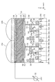
- FIG. 2 is a schematic cross-sectional view showing a cross-sectional structure of two adjacent pixels 10a and 10b among the plurality of pixels 10 shown in FIG.
- the two adjacent pixels 10a and 10b are examples of the first pixel and the second pixel.
- the two adjacent pixels 10a and 10b shown in FIG. 2 both have the same structure.
- one pixel 10a of the two adjacent pixels 10a and 10b will be described.
- the two adjacent pixels 10a and 10b may have a partially different structure.
- the above-mentioned signal detection transistor 24, address transistor 26, and reset transistor 28 are formed on the semiconductor substrate 20.
- the semiconductor substrate 20 is not limited to a substrate whose entire structure is a semiconductor.
- the semiconductor substrate 20 may be an insulating substrate or the like in which a semiconductor layer is provided on the surface on the side where the photosensitive region is formed.
- a P-type silicon (Si) substrate is used as the semiconductor substrate 20 will be described.
- a plug 52, a wiring 53, a contact plug 54, and a contact plug 55 are provided in the interlayer insulating layer 50.
- the wiring 53 may be a part of the wiring layer 56.
- the plug 52, the wiring 53, the contact plug 54, and the contact plug 55 are each formed of a conductive material.
- the plug 52 and the wiring 53 are made of a metal such as copper.
- the contact plugs 54 and 55 are formed of, for example, polysilicon that has been imparted conductivity by doping with impurities.
- the plug 52, the wiring 53, the contact plug 54, and the contact plug 55 may be formed of the same material, or may be formed of different materials.
- the photoelectric conversion unit 13 is arranged between the pixel electrode 11, the counter electrode 12, the photoelectric conversion layer 15 arranged between the pixel electrode 11 and the counter electrode 12, and the pixel electrode 11 and the photoelectric conversion layer 15. Also includes an electron blocking layer 16.
- the photoelectric conversion unit 13 includes a pixel electrode 11, an electron blocking layer 16 located on the pixel electrode 11, a counter electrode 12 of the electron blocking layer 16 facing the opposite side of the pixel electrode 11, and an electron blocking layer.
- a photoelectric conversion layer 15 located between the 16 and the counter electrode 12 is included.
- the electron blocking layer 16 is an example of a first charge blocking layer
- the counter electrode 12 is an example of a second electrode.
- the counter electrode 12 and the photoelectric conversion layer 15 are formed so as to straddle two adjacent pixels 10a and 10b.
- the counter electrode 12 and the photoelectric conversion layer 15 may be formed over the other pixels 10.
- the pixel electrodes 11 are provided on the two adjacent pixels 10a and 10b, respectively.
- the pixel electrode 11 of the pixel 10a is electrically separated from the pixel electrode 11 of the pixel 10b by being spatially separated from the pixel electrode 11 of the adjacent pixel 10b.
- the pixel electrodes 11 of the other pixels 10 not shown in FIG. 2 and the pixel electrodes 11 are provided for each pixel 10.
- At least one of the counter electrode 12 and the photoelectric conversion layer 15 may be provided separately for each pixel 10.
- the counter electrode 12 has a connection with the voltage supply circuit 32. Further, as shown in FIG. 2, the counter electrode 12 is formed so as to straddle two adjacent pixels 10a and 10b. Therefore, it is possible to collectively apply a counter electrode voltage of a desired magnitude from the voltage supply circuit 32 between the two adjacent pixels 10a and 10b via the counter electrode 12.
- the counter electrode 12 may be further formed over a plurality of pixels 10 (not shown in FIG. 2). If a counter electrode voltage of a desired magnitude can be applied from the voltage supply circuit 32, the counter electrode 12 is provided separately for each of the two adjacent pixels 10a and 10b and a plurality of pixels 10 (not shown). It may have been.
- the material of the photoelectric conversion layer 15 may be a quantum dot material or a quantum well material having a quantum confinement effect.
- Quantum dot materials include, for example, PbS, InSb and Ge quantum dots.
- the conductivity of the signal charge of the electron blocking layer 16 may be higher than the conductivity of the signal charge of the photoelectric conversion layer 15 from the viewpoint of improving the charge extraction speed and efficiency.
- a method of separating the photoelectric conversion layer 15 for each pixel can be considered, but when the photoelectric conversion layer 15 is patterned, the dark current increases due to the damage to the photoelectric conversion layer 15, and the image quality is improved. Will deteriorate. This effect becomes more remarkable when a material such as carbon nanotubes or quantum dots having a nanostructure is used for the photoelectric conversion layer 15.
- the flatness of the electron blocking layer 16 and the resistance layer 17 affects the flatness of the photoelectric conversion layer 15 formed thereafter. Further, since the flatness of the photoelectric conversion layer 15 has a problem of affecting the sensitivity variation due to the thickness change for each pixel, it is possible to reduce the sensitivity variation of the image pickup apparatus in this configuration.
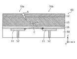
- the individual electron blocking layers 16 and the individual pixel electrodes 11 of the two adjacent pixels 10e and 10f are formed in the interlayer insulating layers 50 and 51, and the interlayers are formed.
- the two electron blocking layers 16 are insulated by the insulating layer 51. Therefore, since the signal charge cannot move between the electron blocking layer 16 of the pixel 10e and the electron blocking layer 16 of the pixel 10f, the movement of the signal charge between the two adjacent pixels 10e and 10f is suppressed, and the colors are mixed. Can be reduced.
- the electron blocking layer 16 is embedded in the interlayer insulating layers 50 and 51, and the step between the upper surface of the electron blocking layer 16 and the upper surface of the interlayer insulating layers 50 and 51 is reduced, so that the photoelectric conversion laminated on the electronic blocking layer 16 is reduced.
- the layer 15 can be easily formed flat, and the occurrence of cracks in the photoelectric conversion layer 15 can be suppressed.
- a polishing process such as CMP Is convenient to use.
- a polishing process such as CMP can be easily used.
- the area of the electron blocking layer 16 is smaller than the area of the pixel electrode 11 in the corresponding pixel in the plan view. Further, the signal charge generated in the photoelectric conversion layer 15 is more likely to move in the electron blocking layer 16 than in the interlayer insulating layer 51. That is, the signal charge collected by the pixel electrode 11 passes through the electron blocking layer 16 corresponding to each pixel and moves to the pixel electrode 11. Since the area of the electron blocking layer 16 is smaller than the area of the pixel electrode 11 in the corresponding pixel in the plan view, the electrons of the pixel 10h adjacent to the pixel 10g are derived from the charge to be collected by the pixel electrode 11 of the pixel 10g.
- the distance to the blocking layer 16 is increased. Therefore, it becomes difficult for the electric charge to be captured by the pixel electrode 11 of the pixel 10g to be collected by the pixel electrode 11 of the pixel 10h, and the color mixing between the two adjacent pixels 10h and 10g can be suppressed.
- the fourth embodiment is different from the first embodiment in that a shield electrode is provided between the two pixel electrodes and an electron blocking layer is arranged on the shield electrode.
- a shield electrode is provided between the two pixel electrodes and an electron blocking layer is arranged on the shield electrode.
- the shield electrode 11a is located between the pixel electrodes 11 of the two adjacent pixels 70e and 70f, and by supplying a fixed potential, the signal charge generated in the photoelectric conversion layer 15 is generated by the two adjacent pixels. Signal charges can be captured when moving across the 70e and 70f. Therefore, by providing the shield electrode 11a, color mixing is suppressed.
- the shield electrode 11a can collect the signal charge that moves across the two adjacent pixels 10i and 10j, so that the color mixing is suppressed.
- the electron blocking layer 16a on the shield electrode 11a is the electron blocking layer 16 of the pixel 10i.
- the electron blocking layer 16 of the pixel 10j are separated. Therefore, the signal charge transferred from the photoelectric conversion layer 15 to the electron blocking layer 16 of the pixel 10i or the electron blocking layer 16 of the pixel 10j is unlikely to move to the electron blocking layer 16a on the shield electrode 11a. Therefore, even when the amount of signal charge to be photoelectrically converted increases, it is difficult for an excessive current to flow through the shield electrode 11a, and damage to the photoelectric conversion unit 13d is suppressed.
- the shapes of the pixel electrode 11, the shield electrode 11a, the electron blocking layer 16 and the electron blocking layer 16a are not particularly limited.
- the pixel electrode 11 and the electron blocking layer 16 may be circular, or may be a regular polygon such as a regular hexagon or a regular octagon.
- the shield electrode 11a and the electron blocking layer 16a may have a plate shape having a plurality of circular or regular polygonal openings provided side by side in a matrix.
- the fifth embodiment is different from the second embodiment in that a shield electrode is provided between the two pixel electrodes and an electron blocking layer is arranged on the shield electrode.
- a shield electrode is provided between the two pixel electrodes and an electron blocking layer is arranged on the shield electrode.
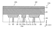
- two adjacent pixels 10k and 10l include a counter electrode 12 and a photoelectric conversion layer 15.
- the counter electrode 12 and the photoelectric conversion layer 15 are formed so as to straddle two adjacent pixels 10k and 10l.
- the two adjacent pixels 10k and 10l each include an individual electron blocking layer 16 and an individual pixel electrode 11.
- the photoelectric conversion unit 13e includes a shield electrode 11a between the pixel electrode 11 of the pixel 10k and the pixel electrode 11 of the pixel 10l.
- the shield electrode 11a is laminated on the interlayer insulating layer 50, and the electron blocking layer 16a is laminated on the shield electrode 11a.
- the electron blocking layer 16a is located between the shield electrode 11a and the photoelectric conversion layer 15.
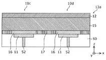
- two adjacent pixels 10m and 10n include a counter electrode 12 and a photoelectric conversion layer 15.
- the counter electrode 12 and the photoelectric conversion layer 15 are formed so as to straddle two adjacent pixels 10m and 10n.
- the two adjacent pixels 10m and 10n each include an individual electron blocking layer 16 and an individual pixel electrode 11.
- the photoelectric conversion unit 13f includes an interlayer insulating layer 51 that insulates the electron blocking layer 16 of the pixel 10m and the electron blocking layer 16 of the pixel 10n.
- the electron blocking layer 16 having 10 m of pixels and the electron blocking layer 16 having 10 n pixels are separated from each other via an interlayer insulating layer 51.
- the photoelectric conversion unit 13f includes a shield electrode 11a between the pixel electrode 11 of the pixel 10m and the pixel electrode 11 of the pixel 10n.
- the shield electrode 11a is formed in the interlayer insulating layer 50, and the upper surface of the shield electrode 11a is in contact with the interlayer insulating layer 51. That is, the photoelectric conversion layer 15 and the shield electrode 11a are insulated by the interlayer insulating layer 51.
- the upper surface of the interlayer insulating layer 51 and the upper surface of the electron blocking layer 16 form a flat surface. Further, in a plan view, the area of the electron blocking layer 16 is larger than that of the pixel electrode 11 in the corresponding pixel.
- the shield electrode 11a is arranged between the pixel electrodes 11 of the two adjacent pixels 10m and 10n.
- a voltage is applied to the shield electrode 11a, it moves across the interface between the photoelectric conversion layer 15 and the interlayer insulating layer 51 located on the shield electrode 11a, straddling the two adjacent pixels 10m and 10n.
- the signal charge is attracted and the color mixing can be reduced.
- the shield electrode 11a and the photoelectric conversion layer 15 are insulated by the interlayer insulating layer 51, the collection of signal charges of the shield electrode 11a is restricted. Therefore, even when the amount of signal charge to be photoelectrically converted increases, an excessive current does not flow to the shield electrode 11a, so that damage to the photoelectric conversion unit 13f is suppressed.
- FIG. 16 is a schematic cross-sectional view showing a cross-sectional structure of a photoelectric conversion unit 13 g of an imaging device according to another example of the present embodiment.
- FIG. 16 shows a photoelectric conversion unit 13g formed so as to straddle two adjacent pixels 10o and 10p. Note that FIG. 16 also shows a part of the interlayer insulating layer 50.
- FIG. 17 is a plan view showing a plan layout of the pixel electrode 11, the shield electrode 11a, and the electron blocking layer 16 of the image pickup apparatus according to another example of the present embodiment. In FIG. 17, the configurations other than the pixel electrode 11, the shield electrode 11a, and the electron blocking layer 16 are not shown.
- two adjacent pixels 10o and 10p include a counter electrode 12 and a photoelectric conversion layer 15.
- the counter electrode 12 and the photoelectric conversion layer 15 are formed so as to straddle two adjacent pixels 10o and 10p.
- the two adjacent pixels 10o and 10p each include an individual electron blocking layer 16 and an individual pixel electrode 11.
- the photoelectric conversion unit 13g includes an interlayer insulating layer 51 that insulates the electron blocking layer 16 of the pixel 10o and the electron blocking layer 16 of the pixel 10p.
- the electron blocking layer 16 of the pixel 10o and the electron blocking layer 16 of the pixel 10p are separated via an interlayer insulating layer 51.
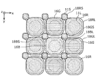
- the seventh embodiment is different from the first embodiment in that pixel electrodes of two sizes, large and small, are provided, and a color filter is provided above the photoelectric conversion unit.
- the differences from the first to sixth embodiments will be mainly described, and the common points will be omitted or simplified.
- FIG. 18 is a plan view showing a plan layout of pixel electrodes 11L and 11S, electron blocking layers 16R, 16G and 16B, and color filters 18RL, 18RS, 18GL, 18GS, 18BL and 18BS of the image pickup apparatus according to the present embodiment. ..
- the configurations other than the pixel electrodes 11L and 11S, the electron blocking layers 16R, 16G and 16B, and the color filters 18RL, 18RS, 18GL, 18GS, 18BL and 18BS are not shown.
- the electron blocking layer is patterned according to the pattern of the color filter, so that the effects such as improvement of area utilization efficiency and improvement of yield can be further obtained.
- the system controller 603 controls the entire camera system 600.
- the system controller 603 can be realized, for example, by a microcomputer.
- a high-quality camera system can be provided by using the image pickup apparatus according to any one of the first to seventh embodiments.
- the photoelectric conversion unit has a configuration including a counter electrode, a photoelectric conversion layer, an electron blocking layer, and a pixel electrode, but the present invention is not limited to this.
- the photoelectric conversion unit may further include a charge blocking layer and the like other than the charge transport layer and the electron blocking layer.
- the photoelectric conversion layer of the photoelectric conversion unit is not limited to one, and a plurality of photoelectric conversion layers may be laminated.
Abstract
An imaging device according to an aspect of the present disclosure is provided with a first pixel and a second pixel adjacent to the first pixel. Each of the first pixel and the second pixel includes: a first electrode; a second electrode positioned over the first electrode and opposing the first electrode; a photoelectric conversion layer positioned between the first electrode and the second electrode; and a first charge blocking layer positioned between the first electrode and the photoelectric conversion layer. The first charge blocking layer of the first pixel and the first charge blocking layer of the second pixel are separated from each other. The photoelectric conversion layer is disposed across the first pixel and the second pixel. In a plan view, the area of the first charge blocking layer in the first pixel is greater than the area of the first electrode in the first pixel, and the area of the first charge blocking layer in the second pixel is greater than the area of the first electrode in the second pixel.
Description
本開示は、撮像装置に関する。
This disclosure relates to an imaging device.
近年、光電変換素子が半導体基板上に設けられた積層型撮像装置が実現されている。積層型撮像装置では、半導体基板と異なる材料によって光電変換素子の光電変換層を形成することができる。このため、例えば、特許文献1および2に開示されているように、シリコンなどの従来の半導体材料とは異なる無機材料または有機材料によって光電変換層を形成することが可能であり、従来とは異なる波長帯域に感度を有する等、従来の撮像装置とは異なる物性または機能を有する撮像装置が実現可能である。また、積層型撮像装置では、信号電荷を取り出すための電極から信号電荷とは異なる電荷が光電変換層へ流入することを抑制するために、電荷ブロッキング層が光電変換層と電極との間に積層される場合がある。
In recent years, a laminated image pickup device in which a photoelectric conversion element is provided on a semiconductor substrate has been realized. In the laminated image pickup apparatus, the photoelectric conversion layer of the photoelectric conversion element can be formed of a material different from that of the semiconductor substrate. Therefore, for example, as disclosed in Patent Documents 1 and 2, it is possible to form the photoelectric conversion layer with an inorganic material or an organic material different from the conventional semiconductor material such as silicon, which is different from the conventional one. It is possible to realize an imaging device having physical properties or functions different from those of a conventional imaging device, such as having sensitivity in a wavelength band. Further, in the laminated image pickup apparatus, a charge blocking layer is laminated between the photoelectric conversion layer and the electrode in order to prevent a charge different from the signal charge from flowing into the photoelectric conversion layer from the electrode for extracting the signal charge. May be done.
積層型撮像装置において、電荷取出し速度および効率を上げるため電荷ブロッキング層および光電変換層の電気伝導度を上げると、隣接画素へ電荷が広がる確率も上がり、混色および解像度低下を招き、画質が低下する。また、混色を防止するために、光電変換層のパターニングを実施すると、光電変換層にダメージが入り光電変換層で発生する暗電流が多くなり、画質を低下させてしまう。
In a stacked image pickup device, if the electric conductivity of the charge blocking layer and the photoelectric conversion layer is increased in order to increase the charge extraction speed and efficiency, the probability that the charge spreads to adjacent pixels also increases, which causes color mixing and resolution deterioration, resulting in deterioration of image quality. .. Further, when the photoelectric conversion layer is patterned in order to prevent color mixing, the photoelectric conversion layer is damaged and the dark current generated in the photoelectric conversion layer increases, which deteriorates the image quality.
そこで、本開示では、画質を向上させることができる撮像装置を提供する。
Therefore, in the present disclosure, an imaging device capable of improving image quality is provided.
本開示の一態様に係る撮像装置は、第1画素と、前記第1画素に隣接する第2画素と、を備える。前記第1画素および前記第2画素のそれぞれは、第1電極と、前記第1電極の上方に位置し、前記第1電極に対向する第2電極と、前記第1電極と前記第2電極との間に位置する光電変換層と、前記第1電極と前記光電変換層との間に位置する第1電荷ブロッキング層と、を含む。前記第1画素の前記第1電荷ブロッキング層と、前記第2画素の前記第1電荷ブロッキング層とは分離されている。前記光電変換層は、前記第1画素と前記第2画素とにまたがって配置されている。平面視において、前記第1画素における前記第1電荷ブロッキング層の面積は、前記第1画素における前記第1電極の面積よりも大きい。平面視において、前記第2画素における前記第1電荷ブロッキング層の面積は、前記第2画素における前記第1電極の面積よりも大きい。
The imaging device according to one aspect of the present disclosure includes a first pixel and a second pixel adjacent to the first pixel. Each of the first pixel and the second pixel has a first electrode, a second electrode located above the first electrode and facing the first electrode, and the first electrode and the second electrode. Includes a photoelectric conversion layer located between the above and a first charge blocking layer located between the first electrode and the photoelectric conversion layer. The first charge blocking layer of the first pixel and the first charge blocking layer of the second pixel are separated. The photoelectric conversion layer is arranged so as to straddle the first pixel and the second pixel. In a plan view, the area of the first charge blocking layer in the first pixel is larger than the area of the first electrode in the first pixel. In a plan view, the area of the first charge blocking layer in the second pixel is larger than the area of the first electrode in the second pixel.
また、本開示の一態様に係る撮像装置は、第1画素と、前記第1画素に隣接する第2画素と、を備える。前記第1画素および前記第2画素のそれぞれは、第1電極と、前記第1電極の上方に位置し、前記第1電極に対向する第2電極と、前記第1電極と前記第2電極との間に位置する光電変換層と、前記第1電極と前記光電変換層との間に位置する第1電荷ブロッキング層と、を含む。前記第1画素の前記第1電荷ブロッキング層と、前記第2画素の前記第1電荷ブロッキング層とは分離されている。前記光電変換層は、前記第1画素と前記第2画素とにまたがって配置されている。平面視において、前記第1画素における前記第1電荷ブロッキング層の面積は、前記第1画素における前記第1電極の面積よりも小さい。平面視において、前記第2画素における前記第1電荷ブロッキング層の面積は、前記第2画素における前記第1電極の面積よりも小さい。
Further, the imaging device according to one aspect of the present disclosure includes a first pixel and a second pixel adjacent to the first pixel. Each of the first pixel and the second pixel has a first electrode, a second electrode located above the first electrode and facing the first electrode, and the first electrode and the second electrode. Includes a photoelectric conversion layer located between the above and a first charge blocking layer located between the first electrode and the photoelectric conversion layer. The first charge blocking layer of the first pixel and the first charge blocking layer of the second pixel are separated. The photoelectric conversion layer is arranged so as to straddle the first pixel and the second pixel. In a plan view, the area of the first charge blocking layer in the first pixel is smaller than the area of the first electrode in the first pixel. In a plan view, the area of the first charge blocking layer in the second pixel is smaller than the area of the first electrode in the second pixel.
本開示の一態様によれば、画質を向上させることができる撮像装置を提供できる。
According to one aspect of the present disclosure, it is possible to provide an imaging device capable of improving image quality.
(本開示の概要)
本開示の一態様に係る撮像装置は、第1画素と、前記第1画素に隣接する第2画素と、を備える。前記第1画素および前記第2画素のそれぞれは、第1電極と、前記第1電極の上方に位置し、前記第1電極に対向する第2電極と、前記第1電極と前記第2電極との間に位置する光電変換層と、前記第1電極と前記光電変換層との間に位置する第1電荷ブロッキング層と、を含む。前記第1画素の前記第1電荷ブロッキング層と、前記第2画素の前記第1電荷ブロッキング層とは分離されている。前記光電変換層は、前記第1画素と前記第2画素とにまたがって配置されている。平面視において、前記第1画素における前記第1電荷ブロッキング層の面積は、前記第1画素における前記第1電極の面積よりも大きい。平面視において、前記第2画素における前記第1電荷ブロッキング層の面積は、前記第2画素における前記第1電極の面積よりも大きい。 (Summary of this disclosure)
The imaging device according to one aspect of the present disclosure includes a first pixel and a second pixel adjacent to the first pixel. Each of the first pixel and the second pixel is a first electrode, a second electrode located above the first electrode and facing the first electrode, and the first electrode and the second electrode. Includes a photoelectric conversion layer located between the above and a first charge blocking layer located between the first electrode and the photoelectric conversion layer. The first charge blocking layer of the first pixel and the first charge blocking layer of the second pixel are separated. The photoelectric conversion layer is arranged so as to straddle the first pixel and the second pixel. In a plan view, the area of the first charge blocking layer in the first pixel is larger than the area of the first electrode in the first pixel. In a plan view, the area of the first charge blocking layer in the second pixel is larger than the area of the first electrode in the second pixel.
これにより、第1電極に信号電荷を輸送し、信号電荷とは逆の電荷の移動を抑制する第1電荷ブロッキング層が、隣接する2つの画素間で分離されている。そのため、第1電荷ブロッキング層内に移動した信号電荷が隣接する2つの画素にまたがって移動しにくくなり、隣接する2つの画素間での信号電荷の交差が抑制される。よって、混色が抑制されるため、画質を向上させることができる。
As a result, the first charge blocking layer that transports the signal charge to the first electrode and suppresses the movement of the charge opposite to the signal charge is separated between the two adjacent pixels. Therefore, the signal charge that has moved in the first charge blocking layer is less likely to move across the two adjacent pixels, and the intersection of the signal charges between the two adjacent pixels is suppressed. Therefore, since color mixing is suppressed, the image quality can be improved.
また、第1電荷ブロッキング層の面積が、対応する画素における第1電極の面積より大きいため、第1電極と第1電荷ブロッキング層の上に位置する光電変換層とが接触しにくくなる。これにより、第1電極から光電変換層への信号電荷とは逆の電荷の移動を抑制する第1電荷ブロッキング層が機能しやすくなり、暗電流を抑制することができる。よって、暗電流が低減されるため、画質を向上させることができる。
Further, since the area of the first charge blocking layer is larger than the area of the first electrode in the corresponding pixel, it becomes difficult for the first electrode and the photoelectric conversion layer located on the first charge blocking layer to come into contact with each other. As a result, the first charge blocking layer that suppresses the movement of the charge opposite to the signal charge from the first electrode to the photoelectric conversion layer becomes easier to function, and the dark current can be suppressed. Therefore, since the dark current is reduced, the image quality can be improved.
また、例えば、平面視において、前記第1画素における前記第1電極は、前記第1画素における前記第1電荷ブロッキング層の内側に位置し、平面視において、前記第2画素における前記第1電極は、前記第2画素における前記第1電荷ブロッキング層の内側に位置してもよい。
Further, for example, in a plan view, the first electrode in the first pixel is located inside the first charge blocking layer in the first pixel, and in a plan view, the first electrode in the second pixel is located. , May be located inside the first charge blocking layer in the second pixel.
これにより、第1電極が、対応する画素における第1電荷ブロッキング層の内側となるため、第1電極と光電変換層とが接触しなくなる。これにより、第1電荷ブロッキング層を介して第1電極と光電変換層とが分離されるため、光電変換層への信号電荷とは逆の電荷の移動が抑制され、暗電流を抑制することができる。
また、例えば、前記第1画素および前記第2画素のそれぞれにおいて、前記第1電荷ブロッキング層の伝導率は、前記光電変換層の伝導率より大きくてもよい。 As a result, the first electrode is inside the first charge blocking layer in the corresponding pixel, so that the first electrode and the photoelectric conversion layer do not come into contact with each other. As a result, the first electrode and the photoelectric conversion layer are separated from each other via the first charge blocking layer, so that the movement of the charge opposite to the signal charge to the photoelectric conversion layer is suppressed, and the dark current can be suppressed. it can.
Further, for example, in each of the first pixel and the second pixel, the conductivity of the first charge blocking layer may be larger than the conductivity of the photoelectric conversion layer.
また、例えば、上記撮像装置は、前記第1画素の前記第1電荷ブロッキング層および前記第2画素の前記第1電荷ブロッキング層の下方に位置する第1絶縁層と、前記第1画素の前記第1電荷ブロッキング層と前記第2画素の前記第1電荷ブロッキング層との間に位置する第2絶縁層と、をさらに備えてもよい。
Further, for example, the image pickup apparatus includes a first insulating layer located below the first charge blocking layer of the first pixel and the first charge blocking layer of the second pixel, and the first insulating layer of the first pixel. A second insulating layer located between the one charge blocking layer and the first charge blocking layer of the second pixel may be further provided.
これにより、第2絶縁層によって、隣接する2つの画素のそれぞれの第1電荷ブロッキング層が絶縁され、2つの第1電荷ブロッキング層との間で信号電荷が移動できないことから、隣接する2つの画素間での信号電荷の移動がより抑制され、より混色が抑制される。
As a result, the first charge blocking layer of each of the two adjacent pixels is insulated by the second insulating layer, and the signal charge cannot be transferred between the two first charge blocking layers. Therefore, the two adjacent pixels The movement of signal charges between them is more suppressed and the color mixing is more suppressed.
また、例えば、前記第1絶縁層と前記第2絶縁層とは同一の材料を含んでもよい。
Further, for example, the first insulating layer and the second insulating layer may contain the same material.
これにより、第1電荷ブロッキング層の間を絶縁する第2絶縁層を、第1絶縁層と同一の材料で形成できるため、簡便に形成される。
As a result, the second insulating layer that insulates between the first charge blocking layers can be formed of the same material as the first insulating layer, so that the second insulating layer can be easily formed.
また、例えば、上記撮像装置は、前記第2絶縁層に接し、平面視において、前記第1画素の前記第1電極と前記第2画素の前記第1電極との間に位置する第3電極をさらに備えてもよい。
Further, for example, the image pickup apparatus has a third electrode that is in contact with the second insulating layer and is located between the first electrode of the first pixel and the first electrode of the second pixel in a plan view. You may also prepare for it.
これにより、第3電極が、隣接する2つの画素のそれぞれの第1画素の間に配置されるため、第3電極にも電圧を印加することで、光電変換層と第3電極上に位置する第2絶縁層との界面に、隣接する2つの画素間をまたがって移動する信号電荷が引き寄せられる。そのため、隣接する2つの画素間での信号電荷の交差が抑制され、より混色が抑制される。
As a result, the third electrode is arranged between the first pixels of the two adjacent pixels, and therefore, by applying a voltage to the third electrode as well, the third electrode is located on the photoelectric conversion layer and the third electrode. A signal charge that moves across two adjacent pixels is attracted to the interface with the second insulating layer. Therefore, the intersection of signal charges between two adjacent pixels is suppressed, and color mixing is further suppressed.
また、例えば、上記撮像装置は、平面視において、前記第1画素の前記第1電極と前記第2画素の前記第1電極との間に位置する第3電極と、前記第3電極と前記光電変換層との間に位置する第2電荷ブロッキング層と、をさらに備え、前記第1画素の前記第1電荷ブロッキング層および前記第2画素の前記第1電荷ブロッキング層からなる群から選択される少なくとも一方と、前記第2電荷ブロッキング層とは分離されてもよい。
Further, for example, in a plan view, the image pickup apparatus includes a third electrode located between the first electrode of the first pixel and the first electrode of the second pixel, and the third electrode and the photoelectric. A second charge blocking layer located between the conversion layer is further provided, and at least selected from the group consisting of the first charge blocking layer of the first pixel and the first charge blocking layer of the second pixel. On the other hand, the second charge blocking layer may be separated.
これにより、第3電極が、隣接する2つの画素のそれぞれの第1画素の間に配置される。また、第3電極は、第2電荷ブロッキング層を介して光電変換層の下側に配置される。そのため、第3電極にも電圧を印加することで、第3電極が、隣接する2つの画素間をまたがって移動する信号電荷を、第2電荷ブロッキング層を介して捕集する。そのため、隣接する2つの画素間での信号電荷の交差が抑制され、より混色が抑制される。
As a result, the third electrode is arranged between the first pixel of each of the two adjacent pixels. Further, the third electrode is arranged under the photoelectric conversion layer via the second charge blocking layer. Therefore, by applying a voltage to the third electrode as well, the third electrode collects the signal charge moving across two adjacent pixels via the second charge blocking layer. Therefore, the intersection of signal charges between two adjacent pixels is suppressed, and color mixing is further suppressed.
また、例えば、平面視において、前記第2電荷ブロッキング層の面積は、前記第3電極の面積よりも大きくてもよい。
Further, for example, in a plan view, the area of the second charge blocking layer may be larger than the area of the third electrode.
これにより、第2電荷ブロッキング層の面積が、第2電荷ブロッキング層の下に位置する第3電極の面積より大きいため、第3電極と第2電荷ブロッキング層の上に位置する光電変換層との接触箇所が少なくなる。これにより、第3電極から光電変換層への信号電荷とは逆の電荷の移動を抑制する第2電荷ブロッキング層が機能しやすくなり、暗電流を抑制することができる。
As a result, the area of the second charge blocking layer is larger than the area of the third electrode located below the second charge blocking layer, so that the third electrode and the photoelectric conversion layer located above the second charge blocking layer are combined. There are fewer contact points. As a result, the second charge blocking layer that suppresses the movement of the charge opposite to the signal charge from the third electrode to the photoelectric conversion layer becomes easier to function, and the dark current can be suppressed.
また、例えば、前記第2電荷ブロッキング層は電子ブロッキング層であってもよい。
Further, for example, the second charge blocking layer may be an electron blocking layer.
これにより、第1電荷ブロッキング層が電子の移動を抑制し、正孔を輸送する。そのため、信号電荷として正孔を用いる場合に、第3電極に信号電荷である正孔を輸送し、信号電荷とは逆の電荷である電子の移動を抑制することができる。
As a result, the first charge blocking layer suppresses the movement of electrons and transports holes. Therefore, when holes are used as the signal charge, the holes, which are the signal charges, can be transported to the third electrode, and the movement of electrons, which are the opposite charges to the signal charges, can be suppressed.
また、例えば、前記光電変換層の一部は、前記第1画素の前記第1電荷ブロッキング層と、前記第2画素の前記第1電荷ブロッキング層との間に位置していてもよい。
Further, for example, a part of the photoelectric conversion layer may be located between the first charge blocking layer of the first pixel and the first charge blocking layer of the second pixel.
これにより、光電変換層が第1電荷ブロッキング層の間に位置するため、第1電極および第1絶縁層の上面を平坦にした後に第1電荷ブロッキング層を形成できる。そのため、第1電極および第1絶縁層の上面に分離されていない第1電荷ブロッキング層を形成し、ドライエッチングなどのパターニングをするのみで隣接する画素の間で分離された第1電荷ブロッキング層を形成できる。よって、第1電荷ブロッキング層の形成後に平坦化プロセスが不要となり、容易に隣接する画素の間で分離された第1電荷ブロッキング層を形成できる。
As a result, since the photoelectric conversion layer is located between the first charge blocking layers, the first charge blocking layer can be formed after the upper surfaces of the first electrode and the first insulating layer are flattened. Therefore, an unseparated first charge blocking layer is formed on the upper surfaces of the first electrode and the first insulating layer, and the first charge blocking layer separated between adjacent pixels is formed only by patterning such as dry etching. Can be formed. Therefore, the flattening process becomes unnecessary after the formation of the first charge blocking layer, and the first charge blocking layer separated between the adjacent pixels can be easily formed.
また、本開示の一態様に係る撮像装置は、第1画素と、前記第1画素に隣接する第2画素と、を備える。前記第1画素および前記第2画素のそれぞれは、第1電極と、前記第1電極の上方に位置し、前記第1電極に対向する第2電極と、前記第1電極と前記第2電極との間に位置する光電変換層と、前記第1電極と前記光電変換層との間に位置する第1電荷ブロッキング層と、を含む。前記第1画素の前記第1電荷ブロッキング層と、前記第2画素の前記第1電荷ブロッキング層とは分離されている。前記光電変換層は、前記第1画素と前記第2画素とにまたがって配置されている。平面視において、前記第1画素における前記第1電荷ブロッキング層の面積は、前記第1画素における前記第1電極の面積よりも小さい。平面視において、前記第2画素における前記第1電荷ブロッキング層の面積は、前記第2画素における前記第1電極の面積よりも小さい。
Further, the imaging device according to one aspect of the present disclosure includes a first pixel and a second pixel adjacent to the first pixel. Each of the first pixel and the second pixel has a first electrode, a second electrode located above the first electrode and facing the first electrode, and the first electrode and the second electrode. Includes a photoelectric conversion layer located between the above and a first charge blocking layer located between the first electrode and the photoelectric conversion layer. The first charge blocking layer of the first pixel and the first charge blocking layer of the second pixel are separated. The photoelectric conversion layer is arranged so as to straddle the first pixel and the second pixel. In a plan view, the area of the first charge blocking layer in the first pixel is smaller than the area of the first electrode in the first pixel. In a plan view, the area of the first charge blocking layer in the second pixel is smaller than the area of the first electrode in the second pixel.
これにより、第1電極に信号電荷を輸送し、信号電荷とは逆の電荷の移動を抑制する第1電荷ブロッキング層が、隣接する2つの画素間で分離されている。そのため、第1電荷ブロッキング層内に移動した信号電荷が隣接する2つの画素にまたがって移動しにくくなり、隣接する2つの画素間での信号電荷の交差が抑制される。よって、混色が抑制されるため、画質を向上させることができる。
As a result, the first charge blocking layer that transports the signal charge to the first electrode and suppresses the movement of the charge opposite to the signal charge is separated between the two adjacent pixels. Therefore, the signal charge that has moved in the first charge blocking layer is less likely to move across the two adjacent pixels, and the intersection of the signal charges between the two adjacent pixels is suppressed. Therefore, since color mixing is suppressed, the image quality can be improved.
また、第1電荷ブロッキング層の面積が、対応する画素における第1電極の面積よりも小さいため、隣接する2つの画素の第1電極の間の距離よりも、隣接する2つの画素の第1電荷ブロッキング層の距離が長くなる。そのため、第1電荷ブロッキング層を介して第1電極へ捕集される信号電荷について、隣接する2つの画素のうち一方の画素の第1電極に捕捉されるべき信号電荷を、他方の画素の第1電極に捕集され難くなる。よって、混色を抑制することができるため、より画質を向上させることができる。
Further, since the area of the first charge blocking layer is smaller than the area of the first electrode in the corresponding pixel, the first charge of the two adjacent pixels is larger than the distance between the first electrodes of the two adjacent pixels. The distance between the blocking layers increases. Therefore, with respect to the signal charge collected to the first electrode via the first charge blocking layer, the signal charge to be captured by the first electrode of one of the two adjacent pixels is set to the second of the other pixel. It becomes difficult to be collected by one electrode. Therefore, since color mixing can be suppressed, the image quality can be further improved.
また、例えば、上記撮像装置は、前記第1画素の前記第1電荷ブロッキング層および前記第2画素の前記第1電荷ブロッキング層の下方に位置する第1絶縁層と、前記第1画素の前記第1電荷ブロッキング層と前記第2画素の前記第1電荷ブロッキング層との間に位置する第2絶縁層と、をさらに備えてもよい。
Further, for example, the image pickup apparatus includes a first insulating layer located below the first charge blocking layer of the first pixel and the first charge blocking layer of the second pixel, and the first insulating layer of the first pixel. A second insulating layer located between the one charge blocking layer and the first charge blocking layer of the second pixel may be further provided.
これにより、第2絶縁層により隣接する2つの画素のそれぞれの第1電荷ブロッキング層が絶縁され、2つの第1電荷ブロッキング層との間で信号電荷が移動できないことから、隣接する2つの画素間での信号電荷の移動がより抑制され、より混色が抑制される。
As a result, the first charge blocking layer of each of the two adjacent pixels is insulated by the second insulating layer, and the signal charge cannot be transferred between the two first charge blocking layers. Therefore, the signal charge cannot be transferred between the two adjacent pixels. The movement of the signal charge in the above is more suppressed, and the color mixing is more suppressed.
また、例えば、前記第1電荷ブロッキング層は電子ブロッキング層であってもよい。
Further, for example, the first charge blocking layer may be an electron blocking layer.
これにより、第1電荷ブロッキング層が電子の移動を抑制し、正孔を輸送する。そのため、信号電荷として正孔を用いる場合に、第1電極に信号電荷である正孔を輸送し、信号電荷とは逆の電荷である電子の移動を抑制することができる。
As a result, the first charge blocking layer suppresses the movement of electrons and transports holes. Therefore, when holes are used as the signal charge, the holes, which are the signal charges, can be transported to the first electrode, and the movement of electrons, which are the opposite charges to the signal charges, can be suppressed.
以下、図面を参照しながら、本開示に係る撮像装置の実施の形態について説明する。なお、本開示は、以下の実施の形態に限定されない。また、本開示の効果を奏する範囲を逸脱しない範囲で、適宜変更は可能である。さらに、一の実施の形態と他の実施の形態とを組み合わせることも可能である。以下の説明において、同一または類似する構成要素については、同一の参照符号を付している。また、重複する説明は省略する場合がある。
Hereinafter, embodiments of the imaging apparatus according to the present disclosure will be described with reference to the drawings. The present disclosure is not limited to the following embodiments. In addition, changes can be made as appropriate without departing from the scope of the effects of the present disclosure. Further, it is possible to combine one embodiment with another. In the following description, the same or similar components are designated by the same reference numerals. In addition, duplicate explanations may be omitted.
また、本明細書において、等しいなどの要素間の関係性を示す用語、および、正方形または円形などの要素の形状を示す用語、ならびに、数値範囲は、厳格な意味のみを表す表現ではなく、実質的に同等な範囲、例えば数%程度の差異をも含むことを意味する表現である。
Further, in the present specification, terms indicating relationships between elements such as equals, terms indicating the shape of elements such as squares or circles, and numerical ranges are not expressions that express only strict meanings, but are substantial. It is an expression meaning that the same range, for example, a difference of about several percent is included.
また、本明細書において、「上方」および「下方」という用語は、絶対的な空間認識における上方向(鉛直上方)および下方向(鉛直下方)を指すものではなく、積層構成における積層順を基に相対的な位置関係により規定される用語として用いる。また、「上方」および「下方」という用語は、2つの構成要素が互いに間隔を空けて配置されて2つの構成要素の間に別の構成要素が存在する場合のみならず、2つの構成要素が互いに密着して配置されて2つの構成要素が接する場合にも適用される。
Further, in the present specification, the terms "upper" and "lower" do not refer to the upward direction (vertically upward) and the downward direction (vertically downward) in absolute spatial recognition, but are based on the stacking order in the stacking configuration. It is used as a term defined by the relative positional relationship with. Also, the terms "upper" and "lower" are used not only when the two components are spaced apart from each other and another component exists between the two components, but also when the two components It also applies when the two components are placed in close contact with each other and touch each other.
(実施の形態1)
[撮像装置の回路構成]
まず本実施の形態に係る撮像装置の回路構成について、図1を用いて説明する。 (Embodiment 1)
[Circuit configuration of imaging device]
First, the circuit configuration of the image pickup apparatus according to the present embodiment will be described with reference to FIG.
[撮像装置の回路構成]
まず本実施の形態に係る撮像装置の回路構成について、図1を用いて説明する。 (Embodiment 1)
[Circuit configuration of imaging device]
First, the circuit configuration of the image pickup apparatus according to the present embodiment will be described with reference to FIG.
図1は、本実施の形態に係る撮像装置の例示的な回路構成を示す模式的な図である。図1に示される撮像装置100は、2次元に配列された複数の画素10を含む画素アレイPAを有する。図1は、画素10が2行2列のマトリクス状に配置された例を模式的に示している。撮像装置100における画素10の数および配置は、図1に示す例に限定されない。例えば、撮像装置100は、複数の画素10が1列に並んだラインセンサであってもよい。
FIG. 1 is a schematic diagram showing an exemplary circuit configuration of the image pickup apparatus according to the present embodiment. The image pickup apparatus 100 shown in FIG. 1 has a pixel array PA including a plurality of pixels 10 arranged in two dimensions. FIG. 1 schematically shows an example in which pixels 10 are arranged in a matrix of 2 rows and 2 columns. The number and arrangement of the pixels 10 in the image pickup apparatus 100 is not limited to the example shown in FIG. For example, the image pickup apparatus 100 may be a line sensor in which a plurality of pixels 10 are arranged in a row.
各画素10は、光電変換部13および信号検出回路14を有する。後に図面を参照して説明するように、光電変換部13は、互いに対向する2つの電極の間に挟まれた光電変換層を有し、入射した光を受けて信号を生成する。光電変換部13は、その全体が、画素10ごとに独立した素子である必要はなく、光電変換部13の例えば一部分が複数の画素10にまたがっていてもよい。信号検出回路14は、光電変換部13によって生成された信号を検出する回路である。この例では、信号検出回路14は、信号検出トランジスタ24およびアドレストランジスタ26を含んでいる。信号検出トランジスタ24およびアドレストランジスタ26は、典型的には、電界効果トランジスタ(FET)であり、ここでは、信号検出トランジスタ24およびアドレストランジスタ26としてNチャネルMOSFET(Metal Oxide Semiconductor Field Effect Transistor)を例示する。信号検出トランジスタ24およびアドレストランジスタ26、ならびに、後述するリセットトランジスタ28などの各トランジスタは、制御端子、入力端子および出力端子を有する。制御端子は、例えばゲートである。入力端子は、ドレインおよびソースの一方であり、例えばドレインである。出力端子は、ドレインおよびソースの他方であり、例えばソースである。
Each pixel 10 has a photoelectric conversion unit 13 and a signal detection circuit 14. As will be described later with reference to the drawings, the photoelectric conversion unit 13 has a photoelectric conversion layer sandwiched between two electrodes facing each other, and receives incident light to generate a signal. The entire photoelectric conversion unit 13 does not have to be an independent element for each pixel 10, and for example, a part of the photoelectric conversion unit 13 may span a plurality of pixels 10. The signal detection circuit 14 is a circuit that detects a signal generated by the photoelectric conversion unit 13. In this example, the signal detection circuit 14 includes a signal detection transistor 24 and an address transistor 26. The signal detection transistor 24 and the address transistor 26 are typically field effect transistors (FETs), and here, as the signal detection transistor 24 and the address transistor 26, an N-channel MOSFET (Metal Oxide Semiconductor Field Effect Transistor) is exemplified. .. Each transistor such as the signal detection transistor 24 and the address transistor 26, and the reset transistor 28 described later has a control terminal, an input terminal, and an output terminal. The control terminal is, for example, a gate. The input terminal is one of the drain and the source, for example, the drain. The output terminal is the other of the drain and the source, for example the source.
図1において模式的に示されるように、信号検出トランジスタ24の制御端子は、光電変換部13との電気的な接続を有する。光電変換部13によって生成される信号電荷は、信号検出トランジスタ24のゲートと光電変換部13との間の電荷蓄積ノード41に蓄積される。ここで、信号電荷は、正孔または電子である。電荷蓄積ノード41は、電荷蓄積部の一例であり、「フローティングディフュージョンノード」とも呼ばれる。本明細書では、電荷蓄積ノードを電荷蓄積領域と呼ぶ。光電変換部13の構造の詳細は、後述する。
As schematically shown in FIG. 1, the control terminal of the signal detection transistor 24 has an electrical connection with the photoelectric conversion unit 13. The signal charge generated by the photoelectric conversion unit 13 is stored in the charge storage node 41 between the gate of the signal detection transistor 24 and the photoelectric conversion unit 13. Here, the signal charge is a hole or an electron. The charge storage node 41 is an example of a charge storage unit, and is also called a “floating diffusion node”. In the present specification, the charge storage node is referred to as a charge storage region. Details of the structure of the photoelectric conversion unit 13 will be described later.
各画素10の光電変換部13は、さらに、対向電極12との接続を有している。対向電極12は、電圧供給回路32に接続されている。電圧供給回路は、対向電極供給回路とも呼ばれる。電圧供給回路32は、任意の可変電圧を供給可能に構成された回路である。電圧供給回路32は、撮像装置100の動作時、対向電極12を介して光電変換部13に所定の電圧を供給する。電圧供給回路32は、特定の電源回路に限定されず、所定の電圧を生成する回路であってもよく、他の電源から供給された電圧を所定の電圧に変換する回路であってもよい。
The photoelectric conversion unit 13 of each pixel 10 further has a connection with the counter electrode 12. The counter electrode 12 is connected to the voltage supply circuit 32. The voltage supply circuit is also called a counter electrode supply circuit. The voltage supply circuit 32 is a circuit configured to be able to supply an arbitrary variable voltage. The voltage supply circuit 32 supplies a predetermined voltage to the photoelectric conversion unit 13 via the counter electrode 12 during the operation of the image pickup apparatus 100. The voltage supply circuit 32 is not limited to a specific power supply circuit, and may be a circuit that generates a predetermined voltage, or may be a circuit that converts a voltage supplied from another power supply into a predetermined voltage.
電圧供給回路32から光電変換部13に供給される電圧が、互いに異なる複数の電圧の間で切り替えられることにより、光電変換部13からの電荷蓄積ノード41への信号電荷の蓄積の開始および終了が制御される。また、上記の制御は、電荷蓄積ノード41側の電圧もしくは後述する画素電極の電圧を制御することでも同等の機能が実現可能である。換言すれば、本実施の形態では、電圧供給回路32から光電変換部13に供給される電圧、または、電荷蓄積ノード41もしくは画素電極の初期電圧を切り替えることによって、電子シャッタ動作が実行される。撮像装置100の動作の例は、後述する。図1に示される構成においては、電荷蓄積ノード41と画素電極とは接続されており、同一の電位となる。
By switching the voltage supplied from the voltage supply circuit 32 to the photoelectric conversion unit 13 between a plurality of different voltages, the start and end of the accumulation of signal charge from the photoelectric conversion unit 13 to the charge storage node 41 can be started. Be controlled. Further, the above control can realize the same function by controlling the voltage on the charge storage node 41 side or the voltage of the pixel electrode described later. In other words, in the present embodiment, the electronic shutter operation is executed by switching the voltage supplied from the voltage supply circuit 32 to the photoelectric conversion unit 13 or the initial voltage of the charge storage node 41 or the pixel electrode. An example of the operation of the image pickup apparatus 100 will be described later. In the configuration shown in FIG. 1, the charge storage node 41 and the pixel electrode are connected and have the same potential.
各画素10は、電源電圧VDDを供給する電源線40との接続を有する。図示するように、電源線40には、信号検出トランジスタ24の入力端子が接続されている。電源線40がソースフォロア電源として機能することにより、信号検出トランジスタ24は、光電変換部13によって生成された信号を増幅して出力する。
Each pixel 10 has a connection with a power supply line 40 that supplies a power supply voltage VDD. As shown in the figure, the input terminal of the signal detection transistor 24 is connected to the power supply line 40. When the power supply line 40 functions as a source follower power supply, the signal detection transistor 24 amplifies and outputs the signal generated by the photoelectric conversion unit 13.
信号検出トランジスタ24の出力端子には、アドレストランジスタ26の入力端子が接続されている。アドレストランジスタ26の出力端子は、画素アレイPAの列ごとに配置された複数の垂直信号線47のうちの1つに接続されている。アドレストランジスタ26の制御端子は、アドレス制御線46に接続されており、アドレス制御線46の電位を制御することにより、信号検出トランジスタ24の出力を、対応する垂直信号線47に選択的に読み出すことができる。
The input terminal of the address transistor 26 is connected to the output terminal of the signal detection transistor 24. The output terminal of the address transistor 26 is connected to one of a plurality of vertical signal lines 47 arranged for each row of the pixel array PA. The control terminal of the address transistor 26 is connected to the address control line 46, and by controlling the potential of the address control line 46, the output of the signal detection transistor 24 is selectively read out to the corresponding vertical signal line 47. Can be done.
図示する例では、アドレス制御線46は、垂直走査回路36に接続されている。垂直走査回路は、「行走査回路」とも呼ばれる。垂直走査回路36は、アドレス制御線46に所定の電圧を印加することにより、各行に配置された複数の画素10を行単位で選択する。これにより、選択された画素10の信号の読み出しと、電荷蓄積ノード41のリセットとが実行される。
In the illustrated example, the address control line 46 is connected to the vertical scanning circuit 36. The vertical scan circuit is also called a "row scan circuit". The vertical scanning circuit 36 selects a plurality of pixels 10 arranged in each row in units of rows by applying a predetermined voltage to the address control line 46. As a result, the signal of the selected pixel 10 is read out and the charge storage node 41 is reset.
垂直信号線47は、画素アレイPAからの画素信号を周辺回路へ伝達する主信号線である。垂直信号線47には、カラム信号処理回路37が接続される。カラム信号処理回路は、「行信号蓄積回路」とも呼ばれる。カラム信号処理回路37は、相関二重サンプリングに代表される雑音抑圧信号処理およびアナログ-デジタル変換(AD変換)などを行う。図示するように、カラム信号処理回路37は、画素アレイPAにおける画素10の各列に対応して設けられる。これらのカラム信号処理回路37には、水平信号読み出し回路38が接続される。水平信号読み出し回路は、「列走査回路」とも呼ばれる。水平信号読み出し回路38は、複数のカラム信号処理回路37から水平共通信号線49に信号を順次読み出す。
The vertical signal line 47 is a main signal line that transmits a pixel signal from the pixel array PA to peripheral circuits. A column signal processing circuit 37 is connected to the vertical signal line 47. The column signal processing circuit is also called a "row signal storage circuit". The column signal processing circuit 37 performs noise suppression signal processing represented by correlated double sampling, analog-to-digital conversion (AD conversion), and the like. As shown, the column signal processing circuit 37 is provided corresponding to each row of pixels 10 in the pixel array PA. A horizontal signal reading circuit 38 is connected to these column signal processing circuits 37. The horizontal signal readout circuit is also called a "column scanning circuit". The horizontal signal reading circuit 38 sequentially reads signals from the plurality of column signal processing circuits 37 to the horizontal common signal line 49.
画素10は、リセットトランジスタ28を有する。リセットトランジスタ28は、例えば、信号検出トランジスタ24およびアドレストランジスタ26と同様に、電界効果トランジスタである。以下では、特に断りの無い限り、リセットトランジスタ28としてNチャネルMOSFETを適用した例を説明する。図示するように、リセットトランジスタ28は、リセット電圧Vrを供給するリセット電圧線44と、電荷蓄積ノード41との間に接続される。リセットトランジスタ28の制御端子は、リセット制御線48に接続されており、リセット制御線48の電位を制御することによって、電荷蓄積ノード41の電位をリセット電圧Vrにリセットすることができる。この例では、リセット制御線48が、垂直走査回路36に接続されている。したがって、垂直走査回路36がリセット制御線48に所定の電圧を印加することにより、各行に配置された複数の画素10を行単位でリセットすることが可能である。
Pixel 10 has a reset transistor 28. The reset transistor 28 is, for example, a field effect transistor similar to the signal detection transistor 24 and the address transistor 26. Hereinafter, unless otherwise specified, an example in which an N-channel MOSFET is applied as the reset transistor 28 will be described. As shown, the reset transistor 28 is connected between the reset voltage line 44 that supplies the reset voltage Vr and the charge storage node 41. The control terminal of the reset transistor 28 is connected to the reset control line 48, and the potential of the charge storage node 41 can be reset to the reset voltage Vr by controlling the potential of the reset control line 48. In this example, the reset control line 48 is connected to the vertical scanning circuit 36. Therefore, the vertical scanning circuit 36 can reset the plurality of pixels 10 arranged in each row in units of rows by applying a predetermined voltage to the reset control line 48.
この例では、リセットトランジスタ28にリセット電圧Vrを供給するリセット電圧線44が、リセット電圧源34に接続されている。リセット電圧源は、「リセット電圧供給回路」とも呼ばれる。リセット電圧源34は、撮像装置100の動作時にリセット電圧線44に所定のリセット電圧Vrを供給可能な構成を有していればよく、上述の電圧供給回路32と同様に、特定の電源回路に限定されない。電圧供給回路32およびリセット電圧源34の各々は、単一の電圧供給回路の一部分であってもよいし、独立した別個の電圧供給回路であってもよい。なお、電圧供給回路32およびリセット電圧源34の一方または両方が、垂直走査回路36の一部分であってもよい。あるいは、電圧供給回路32からの対向電極電圧および/またはリセット電圧源34からのリセット電圧Vrが、垂直走査回路36を介して各画素10に供給されてもよい。
In this example, the reset voltage line 44 that supplies the reset voltage Vr to the reset transistor 28 is connected to the reset voltage source 34. The reset voltage source is also called a "reset voltage supply circuit". The reset voltage source 34 may have a configuration capable of supplying a predetermined reset voltage Vr to the reset voltage line 44 during the operation of the image pickup apparatus 100, and may be supplied to a specific power supply circuit as in the voltage supply circuit 32 described above. Not limited. Each of the voltage supply circuit 32 and the reset voltage source 34 may be a part of a single voltage supply circuit or may be an independent and separate voltage supply circuit. One or both of the voltage supply circuit 32 and the reset voltage source 34 may be a part of the vertical scanning circuit 36. Alternatively, the counter electrode voltage from the voltage supply circuit 32 and / or the reset voltage Vr from the reset voltage source 34 may be supplied to each pixel 10 via the vertical scanning circuit 36.
リセット電圧Vrとして、信号検出回路14の電源電圧VDDを用いることも可能である。この場合、各画素10に電源電圧を供給する電圧供給回路(図1において不図示)と、リセット電圧源34とを共通化し得る。また、電源線40と、リセット電圧線44を共通化できるので、画素アレイPAにおける配線を単純化し得る。ただし、リセット電圧Vrと、信号検出回路14の電源電圧VDDとに互いに異なる電圧を用いることは、撮像装置100のより柔軟な制御を可能にする。
It is also possible to use the power supply voltage VDD of the signal detection circuit 14 as the reset voltage Vr. In this case, the voltage supply circuit (not shown in FIG. 1) that supplies the power supply voltage to each pixel 10 and the reset voltage source 34 can be shared. Further, since the power supply line 40 and the reset voltage line 44 can be shared, the wiring in the pixel array PA can be simplified. However, using different voltages for the reset voltage Vr and the power supply voltage VDD of the signal detection circuit 14 enables more flexible control of the image pickup apparatus 100.
[画素の断面構造]
次に、本実施の形態に係る撮像装置100の画素の断面構造について、図2を用いて説明する。 [Cross-sectional structure of pixels]
Next, the cross-sectional structure of the pixels of theimage pickup apparatus 100 according to the present embodiment will be described with reference to FIG.
次に、本実施の形態に係る撮像装置100の画素の断面構造について、図2を用いて説明する。 [Cross-sectional structure of pixels]
Next, the cross-sectional structure of the pixels of the
図2は、図1に示される複数の画素10のうち、隣接する2つの画素10aおよび10bの断面構造を示す概略断面図である。隣接する2つの画素10aおよび10bは、第1画素および第2画素の一例である。図2に示される隣接する2つの画素10aおよび10bは、いずれも同じ構造である。以下では隣接する2つの画素10aおよび10bのうちの1つの画素10aについて説明する。隣接する2つの画素10aおよび10bは、一部が異なる構造を有していてもよい。図2に例示する構成では、上述の信号検出トランジスタ24、アドレストランジスタ26およびリセットトランジスタ28が、半導体基板20に形成されている。半導体基板20は、その全体が半導体である基板に限定されない。半導体基板20は、感光領域が形成される側の表面に半導体層が設けられた絶縁性基板などであってもよい。ここでは、半導体基板20としてP型シリコン(Si)基板を用いる例を説明する。
FIG. 2 is a schematic cross-sectional view showing a cross-sectional structure of two adjacent pixels 10a and 10b among the plurality of pixels 10 shown in FIG. The two adjacent pixels 10a and 10b are examples of the first pixel and the second pixel. The two adjacent pixels 10a and 10b shown in FIG. 2 both have the same structure. Hereinafter, one pixel 10a of the two adjacent pixels 10a and 10b will be described. The two adjacent pixels 10a and 10b may have a partially different structure. In the configuration illustrated in FIG. 2, the above-mentioned signal detection transistor 24, address transistor 26, and reset transistor 28 are formed on the semiconductor substrate 20. The semiconductor substrate 20 is not limited to a substrate whose entire structure is a semiconductor. The semiconductor substrate 20 may be an insulating substrate or the like in which a semiconductor layer is provided on the surface on the side where the photosensitive region is formed. Here, an example in which a P-type silicon (Si) substrate is used as the semiconductor substrate 20 will be described.
半導体基板20は、不純物領域26s、24s、24d、28dおよび28sと、画素10間の電気的な分離のための素子分離領域20tとを有する。ここでは、不純物領域26s、24s、24d、28dおよび28sはN型領域である。また、素子分離領域20tは、不純物領域24dと不純物領域28dとの間にも設けられている。素子分離領域20tは、例えば所定の注入条件のもとでアクセプタのイオン注入を行うことによって形成される。
The semiconductor substrate 20 has impurity regions 26s, 24s, 24d, 28d and 28s, and an element separation region 20t for electrical separation between the pixels 10. Here, the impurity regions 26s, 24s, 24d, 28d and 28s are N-type regions. Further, the element separation region 20t is also provided between the impurity region 24d and the impurity region 28d. The device separation region 20t is formed by, for example, performing ion implantation of an acceptor under predetermined implantation conditions.
不純物領域26s、24s、24d、28dおよび28sは、例えば、半導体基板20内に形成された、不純物の拡散層である。図2に模式的に示すように、信号検出トランジスタ24は、不純物領域24sおよび24dと、ゲート電極24gとを含む。ゲート電極24gは、導電性材料を用いて形成される。導電性材料は、例えば、不純物がドープされることにより導電性が付与されたポリシリコンであるが、金属材料でもよい。不純物領域24sおよび24dは、それぞれ、信号検出トランジスタ24の例えばソース領域およびドレイン領域として機能する。不純物領域24sと24dとの間に、信号検出トランジスタ24のチャネル領域が形成される。
The impurity regions 26s, 24s, 24d, 28d and 28s are, for example, a diffusion layer of impurities formed in the semiconductor substrate 20. As schematically shown in FIG. 2, the signal detection transistor 24 includes impurity regions 24s and 24d and a gate electrode 24g. The gate electrode 24g is formed by using a conductive material. The conductive material is, for example, polysilicon to which conductivity is imparted by doping with impurities, but a metallic material may also be used. The impurity regions 24s and 24d function as, for example, a source region and a drain region of the signal detection transistor 24, respectively. A channel region of the signal detection transistor 24 is formed between the impurity regions 24s and 24d.
同様に、アドレストランジスタ26は、不純物領域26sおよび24sと、アドレス制御線46に接続されたゲート電極26gとを含む。ゲート電極26gは、導電性材料を用いて形成される。導電性材料は、例えば、不純物がドープされることにより導電性が付与されたポリシリコンであるが、金属材料でもよい。この例では、信号検出トランジスタ24およびアドレストランジスタ26は、不純物領域24sを共有することによって互いに電気的に接続されている。不純物領域24sは、アドレストランジスタ26の例えばドレイン領域として機能する。不純物領域26sは、アドレストランジスタ26の例えばソース領域として機能する。不純物領域26sは、図2には図示されていない垂直信号線47との接続を有する。なお、不純物領域24sは、信号検出トランジスタ24およびアドレストランジスタ26によって共有されていなくてもよい。具体的には、信号検出トランジスタ24のソース領域とアドレストランジスタ26のドレイン領域とは、半導体基板20内では分離しており、層間絶縁層50内に設けられた配線層を介して電気的に接続されていてもよい。
Similarly, the address transistor 26 includes impurity regions 26s and 24s and a gate electrode 26g connected to the address control line 46. The gate electrode 26g is formed by using a conductive material. The conductive material is, for example, polysilicon to which conductivity is imparted by doping with impurities, but a metallic material may also be used. In this example, the signal detection transistor 24 and the address transistor 26 are electrically connected to each other by sharing an impurity region 24s. The impurity region 24s functions as, for example, a drain region of the address transistor 26. The impurity region 26s functions as, for example, a source region of the address transistor 26. The impurity region 26s has a connection with a vertical signal line 47 (not shown in FIG. 2). The impurity region 24s does not have to be shared by the signal detection transistor 24 and the address transistor 26. Specifically, the source region of the signal detection transistor 24 and the drain region of the address transistor 26 are separated in the semiconductor substrate 20, and are electrically connected via a wiring layer provided in the interlayer insulation layer 50. It may have been.
リセットトランジスタ28は、不純物領域28dおよび28sと、リセット制御線48に接続されたゲート電極28gとを含む。ゲート電極28gは、例えば、導電性材料を用いて形成される。導電性材料は、例えば、不純物がドープされることにより導電性が付与されたポリシリコンであるが、金属材料でもよい。不純物領域28sは、リセットトランジスタ28の例えばソース領域として機能する。不純物領域28sは、図2には図示されていないリセット電圧線44との接続を有する。不純物領域28dは、リセットトランジスタ28の例えばドレイン領域として機能する。
The reset transistor 28 includes impurity regions 28d and 28s and a gate electrode 28g connected to the reset control line 48. The gate electrode 28g is formed using, for example, a conductive material. The conductive material is, for example, polysilicon to which conductivity is imparted by doping with impurities, but a metallic material may also be used. The impurity region 28s functions as, for example, a source region of the reset transistor 28. The impurity region 28s has a connection with a reset voltage line 44 (not shown in FIG. 2). The impurity region 28d functions as, for example, a drain region of the reset transistor 28.
半導体基板20上には、信号検出トランジスタ24、アドレストランジスタ26およびリセットトランジスタ28を覆うように層間絶縁層50が配置されている。層間絶縁層50は、第1絶縁層の一例である。層間絶縁層50は、例えば、二酸化シリコンなどの絶縁性材料から形成される。図示するように、層間絶縁層50中には、配線層56が配置されている。配線層56は、典型的には、銅などの金属から形成され、例えば、上述の垂直信号線47などの信号線または電源線をその一部に含み得る。層間絶縁層50中の絶縁層の層数、および、層間絶縁層50中に配置される配線層56に含まれる層数は、任意に設定可能であり、図2に示す例に限定されない。
On the semiconductor substrate 20, an interlayer insulation layer 50 is arranged so as to cover the signal detection transistor 24, the address transistor 26, and the reset transistor 28. The interlayer insulating layer 50 is an example of the first insulating layer. The interlayer insulating layer 50 is formed of an insulating material such as silicon dioxide. As shown in the figure, the wiring layer 56 is arranged in the interlayer insulating layer 50. The wiring layer 56 is typically made of a metal such as copper and may include, for example, a signal line or power line such as the vertical signal line 47 described above as part thereof. The number of layers of the insulating layer in the interlayer insulating layer 50 and the number of layers included in the wiring layer 56 arranged in the interlayer insulating layer 50 can be arbitrarily set and are not limited to the example shown in FIG.
また、層間絶縁層50中には、図2に示されるように、プラグ52、配線53、コンタクトプラグ54、および、コンタクトプラグ55が設けられている。配線53は、配線層56の一部であってもよい。プラグ52、配線53、コンタクトプラグ54、および、コンタクトプラグ55はそれぞれ、導電性材料を用いて形成されている。例えば、プラグ52および配線53は、銅などの金属から形成されている。コンタクトプラグ54および55は、例えば、不純物がドープされることにより導電性が付与されたポリシリコンから形成されている。なお、プラグ52、配線53、コンタクトプラグ54、および、コンタクトプラグ55は、互いに同じ材料を用いて形成されていてもよく、互いに異なる材料を用いて形成されていてもよい。
Further, as shown in FIG. 2, a plug 52, a wiring 53, a contact plug 54, and a contact plug 55 are provided in the interlayer insulating layer 50. The wiring 53 may be a part of the wiring layer 56. The plug 52, the wiring 53, the contact plug 54, and the contact plug 55 are each formed of a conductive material. For example, the plug 52 and the wiring 53 are made of a metal such as copper. The contact plugs 54 and 55 are formed of, for example, polysilicon that has been imparted conductivity by doping with impurities. The plug 52, the wiring 53, the contact plug 54, and the contact plug 55 may be formed of the same material, or may be formed of different materials.
プラグ52、配線53およびコンタクトプラグ54は、信号検出トランジスタ24と光電変換部13との間の電荷蓄積ノード41の少なくとも一部を構成する。図2に例示する構成において、信号検出トランジスタ24のゲート電極24g、プラグ52、配線53、コンタクトプラグ54および55、ならびに、リセットトランジスタ28のソース領域およびドレイン領域の一方である不純物領域28dは、層間絶縁層50上に位置する光電変換部13の画素電極11によって収集された信号電荷を蓄積する電荷蓄積領域として機能する。画素電極11は、第1電極の一例である。
The plug 52, the wiring 53, and the contact plug 54 form at least a part of the charge storage node 41 between the signal detection transistor 24 and the photoelectric conversion unit 13. In the configuration illustrated in FIG. 2, the gate electrode 24g of the signal detection transistor 24, the plug 52, the wiring 53, the contact plugs 54 and 55, and the impurity region 28d, which is one of the source region and the drain region of the reset transistor 28, are interposed. It functions as a charge storage region for accumulating the signal charge collected by the pixel electrode 11 of the photoelectric conversion unit 13 located on the insulating layer 50. The pixel electrode 11 is an example of the first electrode.
具体的には、光電変換部13の画素電極11は、プラグ52、配線53およびコンタクトプラグ54を介して、信号検出トランジスタ24のゲート電極24gに接続されている。言い換えれば、信号検出トランジスタ24のゲートは、画素電極11と電気的に接続されている。また、画素電極11は、プラグ52、配線53およびコンタクトプラグ55を介して、不純物領域28dにも接続されている。
Specifically, the pixel electrode 11 of the photoelectric conversion unit 13 is connected to the gate electrode 24g of the signal detection transistor 24 via the plug 52, the wiring 53, and the contact plug 54. In other words, the gate of the signal detection transistor 24 is electrically connected to the pixel electrode 11. The pixel electrode 11 is also connected to the impurity region 28d via the plug 52, the wiring 53, and the contact plug 55.
画素電極11によって信号電荷が捕集されることにより、電荷蓄積領域に蓄積された信号電荷の量に応じた電圧が、信号検出トランジスタ24のゲートに印加される。信号検出トランジスタ24は、この電圧を増幅する。信号検出トランジスタ24によって増幅された電圧が、信号電圧としてアドレストランジスタ26を介して選択的に読み出される。
By collecting the signal charge by the pixel electrode 11, a voltage corresponding to the amount of the signal charge accumulated in the charge storage region is applied to the gate of the signal detection transistor 24. The signal detection transistor 24 amplifies this voltage. The voltage amplified by the signal detection transistor 24 is selectively read out as a signal voltage via the address transistor 26.
層間絶縁層50上には、上述の光電変換部13が配置される。別の言い方をすれば、本実施の形態では、図1に示される画素アレイPAを構成する複数の画素10が、半導体基板20中および半導体基板20上に形成されている。半導体基板20を平面視した場合に2次元に配列された複数の画素10は、感光領域を形成する。感光領域は、画素領域とも呼ばれる。図2に示される、隣接する2つの画素10aおよび10b間の距離すなわち、画素ピッチは、例えば2μm程度であってもよい。
The above-mentioned photoelectric conversion unit 13 is arranged on the interlayer insulating layer 50. In other words, in the present embodiment, a plurality of pixels 10 constituting the pixel array PA shown in FIG. 1 are formed in the semiconductor substrate 20 and on the semiconductor substrate 20. When the semiconductor substrate 20 is viewed in a plan view, the plurality of pixels 10 arranged two-dimensionally form a photosensitive region. The photosensitive area is also called a pixel area. The distance between two adjacent pixels 10a and 10b shown in FIG. 2, that is, the pixel pitch may be, for example, about 2 μm.
光電変換部13は、画素電極11と、対向電極12と、光電変換層15と、電子ブロッキング層16とを含む。つまり、複数の画素10のそれぞれは、画素電極11と、画素電極11の上方に位置し、画素電極11に対向する対向電極12と、画素電極11と対向電極12との間に位置する光電変換層15と、画素電極11と光電変換層15との間に位置する電子ブロッキング層16と、を備える。層間絶縁層50は、電子ブロッキング層16の下方に位置する。
The photoelectric conversion unit 13 includes a pixel electrode 11, a counter electrode 12, a photoelectric conversion layer 15, and an electron blocking layer 16. That is, each of the plurality of pixels 10 is positioned above the pixel electrode 11 and the pixel electrode 11, and is located between the counter electrode 12 facing the pixel electrode 11 and the pixel electrode 11 and the counter electrode 12. A layer 15 and an electron blocking layer 16 located between the pixel electrode 11 and the photoelectric conversion layer 15 are provided. The interlayer insulating layer 50 is located below the electron blocking layer 16.
また、図2に示されるように、光電変換部13上には、カラーフィルタ18が配置されていてもよい。カラーフィルタ18は、例えば、赤色光、緑色光または青色光の波長範囲の光を透過させるバンドパスフィルタである。カラーフィルタ18は、ロングパスフィルタまたはノッチフィルタであってもよい。また、カラーフィルタ18は、紫外線または赤外線を透過させるフィルタであってもよい。また、カラーフィルタ18は、透過させる光の透過率を調整できるフィルタであってもよい。
Further, as shown in FIG. 2, a color filter 18 may be arranged on the photoelectric conversion unit 13. The color filter 18 is, for example, a bandpass filter that transmits light in the wavelength range of red light, green light, or blue light. The color filter 18 may be a long-pass filter or a notch filter. Further, the color filter 18 may be a filter that transmits ultraviolet rays or infrared rays. Further, the color filter 18 may be a filter capable of adjusting the transmittance of the transmitted light.
[光電変換部の構成]
以下では、層間絶縁層50上に位置する光電変換部13の具体的な構成について説明する。 [Configuration of photoelectric conversion unit]
Hereinafter, a specific configuration of thephotoelectric conversion unit 13 located on the interlayer insulating layer 50 will be described.
以下では、層間絶縁層50上に位置する光電変換部13の具体的な構成について説明する。 [Configuration of photoelectric conversion unit]
Hereinafter, a specific configuration of the
光電変換部13は、画素電極11と、対向電極12と、画素電極11と対向電極12との間に配置された光電変換層15と、画素電極11と光電変換層15との間に配置された電子ブロッキング層16とを含む。言い換えると、光電変換部13は、画素電極11と、画素電極11上に位置する電子ブロッキング層16と、電子ブロッキング層16の画素電極11とは反対側に対向する対向電極12と、電子ブロッキング層16と対向電極12との間に位置する光電変換層15とを含む。電子ブロッキング層16は、第1電荷ブロッキング層の一例であり、対向電極12は第2電極の一例である。この例では、対向電極12および光電変換層15は、隣接する2つの画素10aおよび10bにまたがって形成されている。対向電極12および光電変換層15は、さらに他の画素10にもまたがって形成されていてもよい。画素電極11は、隣接する2つの画素10aおよび10bそれぞれに設けられている。画素10aの画素電極11は、隣接する画素10bの画素電極11と空間的に分離されることによって、画素10bの画素電極11から電気的に分離されている。図2に示されていない他の画素10の画素電極11についても、同様であり、画素電極11は、画素10ごとに設けられている。なお、対向電極12および光電変換層15の少なくとも1つは、画素10ごとに分離して設けられていてもよい。
The photoelectric conversion unit 13 is arranged between the pixel electrode 11, the counter electrode 12, the photoelectric conversion layer 15 arranged between the pixel electrode 11 and the counter electrode 12, and the pixel electrode 11 and the photoelectric conversion layer 15. Also includes an electron blocking layer 16. In other words, the photoelectric conversion unit 13 includes a pixel electrode 11, an electron blocking layer 16 located on the pixel electrode 11, a counter electrode 12 of the electron blocking layer 16 facing the opposite side of the pixel electrode 11, and an electron blocking layer. A photoelectric conversion layer 15 located between the 16 and the counter electrode 12 is included. The electron blocking layer 16 is an example of a first charge blocking layer, and the counter electrode 12 is an example of a second electrode. In this example, the counter electrode 12 and the photoelectric conversion layer 15 are formed so as to straddle two adjacent pixels 10a and 10b. The counter electrode 12 and the photoelectric conversion layer 15 may be formed over the other pixels 10. The pixel electrodes 11 are provided on the two adjacent pixels 10a and 10b, respectively. The pixel electrode 11 of the pixel 10a is electrically separated from the pixel electrode 11 of the pixel 10b by being spatially separated from the pixel electrode 11 of the adjacent pixel 10b. The same applies to the pixel electrodes 11 of the other pixels 10 not shown in FIG. 2, and the pixel electrodes 11 are provided for each pixel 10. At least one of the counter electrode 12 and the photoelectric conversion layer 15 may be provided separately for each pixel 10.
画素電極11は、光電変換部13で生成された信号電荷を読み出すための電極である。画素電極11は、画素10ごとに少なくとも1つ存在する。画素電極11は、信号検出トランジスタ24のゲート電極24gおよび不純物領域28dに電気的に接続されている。
The pixel electrode 11 is an electrode for reading out the signal charge generated by the photoelectric conversion unit 13. There is at least one pixel electrode 11 for each pixel 10. The pixel electrode 11 is electrically connected to the gate electrode 24g of the signal detection transistor 24 and the impurity region 28d.
画素電極11は、導電性材料を用いて形成されている。導電性材料は、例えば、アルミニウム、銅などの金属、金属窒化物、または、不純物がドープされることにより導電性が付与されたポリシリコンである。
The pixel electrode 11 is formed by using a conductive material. The conductive material is, for example, a metal such as aluminum or copper, a metal nitride, or polysilicon to which conductivity is imparted by doping with impurities.
対向電極12は、例えば、透明な導電性材料から形成される透明電極である。対向電極12は、光電変換層15において光が入射される側に配置される。したがって、光電変換層15には、対向電極12を透過した光が入射する。なお、撮像装置100によって検出される光は、可視光の波長範囲内の光に限定されない。例えば、撮像装置100は、赤外線または紫外線を検出してもよい。ここで、可視光の波長範囲とは、例えば、380nm以上780nm以下である。
The counter electrode 12 is, for example, a transparent electrode formed of a transparent conductive material. The counter electrode 12 is arranged on the side of the photoelectric conversion layer 15 on which light is incident. Therefore, the light transmitted through the counter electrode 12 is incident on the photoelectric conversion layer 15. The light detected by the image pickup apparatus 100 is not limited to the light within the wavelength range of visible light. For example, the image pickup apparatus 100 may detect infrared rays or ultraviolet rays. Here, the wavelength range of visible light is, for example, 380 nm or more and 780 nm or less.
なお、本明細書における「透明」は、検出しようとする波長範囲の光の少なくとも一部を透過することを意味し、可視光の波長範囲全体にわたって光を透過することは必須ではない。本明細書では、赤外線および紫外線を含めた電磁波全般を、便宜上「光」と表現する。
Note that "transparent" in the present specification means that at least a part of light in the wavelength range to be detected is transmitted, and it is not essential to transmit light over the entire wavelength range of visible light. In the present specification, electromagnetic waves in general including infrared rays and ultraviolet rays are referred to as "light" for convenience.
対向電極12は、例えば、ITO、IZO、AZO、FTO、SnO2、TiO2、ZnO2などの透明導電性酸化物(TCO:Transparent Conducting Oxide)を用いて形成される。
The counter electrode 12 is formed by using, for example, a transparent conductive oxide (TCO: Transient Conducting Oxide) such as ITO, IZO, AZO, FTO, SnO 2 , TiO 2 , and ZnO 2 .
図1を参照して説明したように、対向電極12は、電圧供給回路32との接続を有する。また、図2に示されるように、対向電極12は、隣接する2つの画素10aおよび10bにまたがって形成されている。したがって、対向電極12を介して、電圧供給回路32から所望の大きさの対向電極電圧を隣接する2つの画素10aおよび10bの間に一括して印加することが可能である。対向電極12は、さらに図2に示されていない複数の画素10にもまたがって形成されていてもよい。なお、電圧供給回路32から所望の大きさの対向電極電圧を印加することができれば、対向電極12は、隣接する2つの画素10aおよび10bならびに図示されていない複数の画素10ごとに分離して設けられていてもよい。
As described with reference to FIG. 1, the counter electrode 12 has a connection with the voltage supply circuit 32. Further, as shown in FIG. 2, the counter electrode 12 is formed so as to straddle two adjacent pixels 10a and 10b. Therefore, it is possible to collectively apply a counter electrode voltage of a desired magnitude from the voltage supply circuit 32 between the two adjacent pixels 10a and 10b via the counter electrode 12. The counter electrode 12 may be further formed over a plurality of pixels 10 (not shown in FIG. 2). If a counter electrode voltage of a desired magnitude can be applied from the voltage supply circuit 32, the counter electrode 12 is provided separately for each of the two adjacent pixels 10a and 10b and a plurality of pixels 10 (not shown). It may have been.
電圧供給回路32が画素電極11の電位に対する対向電極12の電位を制御することにより、光電変換によって光電変換層15内に生じた正孔-電子対のうち正孔および電子のいずれか一方を、信号電荷として画素電極11によって捕集することができる。例えば信号電荷として正孔を利用する場合、画素電極11よりも対向電極12の電位を高くすることにより、画素電極11によって正孔を選択的に捕集することが可能である。以下では、信号電荷として正孔を利用する場合を例示する。なお、信号電荷として電子を利用することも可能であり、この場合、画素電極11よりも対向電極12の電位を低くすればよい。対向電極12に対向する画素電極11は、対向電極12と画素電極11との間に適切なバイアス電圧が与えられることにより、光電変換層15において光電変換によって発生した正および負の電荷のうちの一方を捕集する。
By controlling the potential of the counter electrode 12 with respect to the potential of the pixel electrode 11, the voltage supply circuit 32 converts either holes or electrons among the hole-electron pairs generated in the photoelectric conversion layer 15 by photoelectric conversion. It can be collected by the pixel electrode 11 as a signal charge. For example, when holes are used as signal charges, holes can be selectively collected by the pixel electrodes 11 by making the potential of the counter electrode 12 higher than that of the pixel electrodes 11. In the following, a case where holes are used as signal charges will be illustrated. It is also possible to use electrons as signal charges. In this case, the potential of the counter electrode 12 may be lower than that of the pixel electrode 11. The pixel electrode 11 facing the counter electrode 12 has a positive and negative charge generated by the photoelectric conversion in the photoelectric conversion layer 15 by applying an appropriate bias voltage between the counter electrode 12 and the pixel electrode 11. Collect one.
光電変換層15は、入射する光を受けて正孔-電子対を発生させる。光電変換層の材料としては、例えば、半導体性の無機材料、または、半導体性の有機材料などが用いられる。
The photoelectric conversion layer 15 receives the incident light to generate a hole-electron pair. As the material of the photoelectric conversion layer, for example, a semiconductor inorganic material, a semiconductor organic material, or the like is used.
光電変換層15の材料は、量子閉じ込め効果を持つ量子ドット材料または量子井戸材料であってもよい。量子ドット材料としては、例えば、PbS、InSbおよびGeの量子ドットが挙げられる。
The material of the photoelectric conversion layer 15 may be a quantum dot material or a quantum well material having a quantum confinement effect. Quantum dot materials include, for example, PbS, InSb and Ge quantum dots.
また、光電変換層15の材料は、カイラリティ選定による波長選択性を持たせたカーボンナノチューブであってもよい。カイラリティ選定による波長選択性を持たせたカーボンナノチューブは、結晶性材料等によるブロードな吸光ピークではなく、シャープかつナローな吸光ピークによる吸収感度特性を持つため、狭帯域波長撮像の実現が可能である。
Further, the material of the photoelectric conversion layer 15 may be carbon nanotubes having wavelength selectivity by selecting chirality. Carbon nanotubes with wavelength selectivity selected by chirality have absorption sensitivity characteristics due to sharp and narrow absorption peaks instead of broad absorption peaks due to crystalline materials, etc., so narrow-band wavelength imaging can be realized. ..
量子ドット材料またはカーボンナノチューブを光電変換層の材料として用いた場合、光電変換層のパターニングを光電変換層の成膜後に行うと、用いられた量子ドット材料またはカーボンナノチューブが明確に欠損ダメージを受ける。その結果、撮像装置の暗電流の増加を招くため、本実施の形態に係る撮像装置の構成とすることで、光電変換層のパターニングを行う場合の光電変換層への欠損ダメージがなく、解像度低下および混色を低減することが可能となる。
When a quantum dot material or carbon nanotube is used as a material for a photoelectric conversion layer, if the photoelectric conversion layer is patterned after the film formation of the photoelectric conversion layer, the quantum dot material or carbon nanotube used is clearly damaged. As a result, the dark current of the imaging device is increased. Therefore, by configuring the imaging device according to the present embodiment, there is no damage to the photoelectric conversion layer when patterning the photoelectric conversion layer, and the resolution is lowered. And it is possible to reduce color mixing.
本実施の形態に係る撮像装置100のように、光電変換層15を回路基板に積層する構成では、CMOS(Complementary Metal Oxide Semiconductor)イメージセンサと異なり、回路基板を構成するSi等とは異なる材料を選択し、光電変換部13を構成できるため、回路基板の持つ波長特性に依らない撮像が実現できる効果が得られる。
In the configuration in which the photoelectric conversion layer 15 is laminated on the circuit board as in the image pickup apparatus 100 according to the present embodiment, unlike the CMOS (Complementary Metal Oxide Semiconductor) image sensor, a material different from Si or the like constituting the circuit board is used. Since the photoelectric conversion unit 13 can be selected and configured, the effect of realizing imaging that does not depend on the wavelength characteristics of the circuit board can be obtained.
電子ブロッキング層16は、隣接する画素電極11から光電変換層15への信号電荷とは逆の電荷である電子の移動を抑制するとともに、光電変換層15で発生した信号電荷である正孔を電極へ輸送する機能を有する。これにより、撮像装置の暗電流が抑制される。電子ブロッキング層16の材料は、例えば、p型半導体であり、具体的には、ニッケル酸化物、酸化銅、酸化クロム、酸化コバルト、酸化チタン、酸化亜鉛などの無機材料からなる半導体が挙げられるが、これに限定されない。p型半導体は、金属酸化物または金属窒化物に不純物をドーピングした無機材料からなるp型半導体であってもよく、具体的には、例えば、シリコン酸化物にリン、ヒ素またはアンチモンなどをドーピングした膜などであってもよい。電子ブロッキング層16の材料には、正孔輸送性有機化合物などの有機材料からなる半導体が用いられてもよい。
The electron blocking layer 16 suppresses the movement of electrons, which is a charge opposite to the signal charge from the adjacent pixel electrode 11, to the photoelectric conversion layer 15, and electrodes holes, which are signal charges generated in the photoelectric conversion layer 15. Has the function of transporting to. As a result, the dark current of the imaging device is suppressed. The material of the electron blocking layer 16 is, for example, a p-type semiconductor, and specific examples thereof include semiconductors made of inorganic materials such as nickel oxide, copper oxide, chromium oxide, cobalt oxide, titanium oxide, and zinc oxide. , Not limited to this. The p-type semiconductor may be a p-type semiconductor made of an inorganic material obtained by doping a metal oxide or a metal nitride with impurities. Specifically, for example, a silicon oxide is doped with phosphorus, arsenic, antimony, or the like. It may be a film or the like. As the material of the electron blocking layer 16, a semiconductor made of an organic material such as a hole-transporting organic compound may be used.
電子ブロッキング層16の材料は、上記のように無機材料であってもよい。電子ブロッキング層16の材料として無機材料を用いることにより、フォトリソグラフィーによる電子ブロッキング層16のパターニングが精度良く容易に実現される。また、電子ブロッキング層16の材料として無機材料を用いた場合には、無機材料は、CMOSプロセスとの親和性も高く、ダスト導入の汚染リスクが低いこと、および、成膜後のCMP(Chemical Mechanical Polishing)研磨により平坦性が確保できることにより、光電変換効率バラつきを低減できる。よって、より高画質な撮像装置が実現される。
The material of the electron blocking layer 16 may be an inorganic material as described above. By using an inorganic material as the material of the electron blocking layer 16, patterning of the electron blocking layer 16 by photolithography can be easily realized with high accuracy. Further, when an inorganic material is used as the material of the electron blocking layer 16, the inorganic material has a high affinity with the CMOS process, has a low risk of contamination due to dust introduction, and has a CMP (Chemical Mechanical) after film formation. Since the flatness can be ensured by polishing) polishing, the variation in photoelectric conversion efficiency can be reduced. Therefore, a higher image quality imaging device is realized.
また、電子ブロッキング層16の信号電荷の伝導率は、電荷取出し速度および効率を向上する観点から、光電変換層15の信号電荷の伝導率よりも高くてもよい。
Further, the conductivity of the signal charge of the electron blocking layer 16 may be higher than the conductivity of the signal charge of the photoelectric conversion layer 15 from the viewpoint of improving the charge extraction speed and efficiency.
光電変換部13における電子ブロッキング層16の構造の詳細は後述する。
Details of the structure of the electron blocking layer 16 in the photoelectric conversion unit 13 will be described later.
本実施の形態においては、光電変換層15から信号電荷として正孔を蓄積し、読み出しを行う場合に、暗電流を低減するための電子ブロッキング層16を設ける構造について述べた。逆に信号電荷として電子を蓄積し、読み出しを行う場合には、第1電荷ブロッキング層として正孔ブロッキング層を、電子ブロッキング層16の代わりに用いればよい。正孔ブロッキング層は、隣接する画素電極11から光電変換層15への正孔の移動を抑制するとともに、光電変換層15で発生した電子を電極へ輸送する機能を有する。正孔ブロッキング層の材料は、例えば、n型半導体である。
In the present embodiment, the structure in which the electron blocking layer 16 for reducing the dark current is provided when holes are accumulated as signal charges from the photoelectric conversion layer 15 and read out is described. On the contrary, when electrons are accumulated as signal charges and read out, a hole blocking layer may be used as the first charge blocking layer instead of the electron blocking layer 16. The hole blocking layer has a function of suppressing the movement of holes from the adjacent pixel electrode 11 to the photoelectric conversion layer 15 and transporting electrons generated in the photoelectric conversion layer 15 to the electrode. The material of the hole blocking layer is, for example, an n-type semiconductor.
次に、本実施の形態に係る撮像装置100の電子ブロッキング層16の積層構造の詳細について説明する。
Next, the details of the laminated structure of the electron blocking layer 16 of the image pickup apparatus 100 according to the present embodiment will be described.
まず、実施の形態1を説明するための比較例1に係る撮像装置について説明する。図3は、比較例1に係る撮像装置の光電変換部60の断面構造を示す概略断面図である。図3には、隣接する2つの画素70aおよび70bにまたがって形成されている光電変換部60が示されている。なお、図3には層間絶縁層50の一部も示されている。以下の光電変換部の断面構造を示す各概略断面図では、光電変換部および層間絶縁層の一部以外の構成については図示されていないが、光電変換部以外の構成については、図2に示される画素10aおよび10bの構成と同じである。
First, the imaging apparatus according to Comparative Example 1 for explaining the first embodiment will be described. FIG. 3 is a schematic cross-sectional view showing the cross-sectional structure of the photoelectric conversion unit 60 of the imaging device according to Comparative Example 1. FIG. 3 shows a photoelectric conversion unit 60 formed so as to straddle two adjacent pixels 70a and 70b. Note that FIG. 3 also shows a part of the interlayer insulating layer 50. In each schematic cross-sectional view showing the cross-sectional structure of the photoelectric conversion unit below, the configuration other than the photoelectric conversion unit and a part of the interlayer insulating layer is not shown, but the configuration other than the photoelectric conversion unit is shown in FIG. The configuration is the same as that of the pixels 10a and 10b.
図3に示されるように、隣接する2つの画素70aおよび70bは、対向電極12、光電変換層15および電子ブロッキング層16を備える。対向電極12、光電変換層15および電子ブロッキング層16は、隣接する2つの画素70aおよび70bにまたがって形成されている。また、隣接する2つの画素70aおよび70bは、それぞれ、個別の画素電極11を備える。そのため、光電変換層15に入射した光Aが光電変換されることにより発生した信号電荷は、矢印Bで示されるように光電変換層15内で画素70aから画素70bへ移動したり、矢印Cで示されるように電子ブロッキング層16内で画素70aおよび70b間を移動したりしやすい。そのため、本来、画素70aの画素電極11に捕捉されるべき電荷が、画素70bの画素電極11に捕集された場合には、隣接する2つの画素70aおよび70b間での混色が発生する。また、同様のメカニズムにより、画素電極11のピッチよりも電荷捕集範囲が拡大することによる解像度低下、および、許容される撮像装置100への光線入射角度が、混色を避けるために制限されることで、入射角度が狭くなってしまうこと等の課題も起こり得る。
As shown in FIG. 3, two adjacent pixels 70a and 70b include a counter electrode 12, a photoelectric conversion layer 15, and an electron blocking layer 16. The counter electrode 12, the photoelectric conversion layer 15, and the electron blocking layer 16 are formed so as to straddle two adjacent pixels 70a and 70b. Further, the two adjacent pixels 70a and 70b each include individual pixel electrodes 11. Therefore, the signal charge generated by the photoelectric conversion of the light A incident on the photoelectric conversion layer 15 moves from the pixel 70a to the pixel 70b in the photoelectric conversion layer 15 as indicated by the arrow B, or is indicated by the arrow C. As shown, it is easy to move between pixels 70a and 70b within the electron blocking layer 16. Therefore, when the electric charge that should be originally captured by the pixel electrode 11 of the pixel 70a is collected by the pixel electrode 11 of the pixel 70b, color mixing occurs between the two adjacent pixels 70a and 70b. Further, by the same mechanism, the resolution is lowered due to the charge collection range expanding beyond the pitch of the pixel electrodes 11, and the permissible angle of light incident on the imaging device 100 is limited in order to avoid color mixing. Therefore, problems such as a narrowing of the incident angle may occur.
光電変換した信号電荷を高速で画素電極11に捕集するために、光電変換層15および電子ブロッキング層16の電気伝導度を向上させようとした場合、この混色に関する課題はより顕著になる。
When the electrical conductivity of the photoelectric conversion layer 15 and the electron blocking layer 16 is to be improved in order to collect the photoelectrically converted signal charge on the pixel electrode 11 at high speed, the problem related to this color mixing becomes more remarkable.
この混色課題を解決する為に、光電変換層15を画素毎に分離する手法も考えられるが、光電変換層15にパターニングを行うと、光電変換層15へのダメージにより暗電流が増加し、画質を劣化させてしまう。この影響は、光電変換層15にナノ構造を持つカーボンナノチューブまたは量子ドット等の材料を用いた場合に、より顕著になる。
In order to solve this color mixing problem, a method of separating the photoelectric conversion layer 15 for each pixel can be considered, but when the photoelectric conversion layer 15 is patterned, the dark current increases due to the damage to the photoelectric conversion layer 15, and the image quality is improved. Will deteriorate. This effect becomes more remarkable when a material such as carbon nanotubes or quantum dots having a nanostructure is used for the photoelectric conversion layer 15.
次に、比較例2に係る撮像装置について説明する。図4は、比較例2に係る撮像装置の光電変換部60aの断面構造を示す概略断面図である。図4には、隣接する2つの画素70cおよび70dにまたがって形成されている光電変換部60aが示されている。なお、図4には層間絶縁層50の一部も示されている。
Next, the imaging device according to Comparative Example 2 will be described. FIG. 4 is a schematic cross-sectional view showing the cross-sectional structure of the photoelectric conversion unit 60a of the imaging device according to Comparative Example 2. FIG. 4 shows a photoelectric conversion unit 60a formed so as to straddle two adjacent pixels 70c and 70d. Note that FIG. 4 also shows a part of the interlayer insulating layer 50.
図4に示されるように、隣接する2つの画素70cおよび70dは、対向電極12および光電変換層15を備える。対向電極12および光電変換層15は、隣接する2つの画素70cおよび70dにまたがって形成されている。また、隣接する2つの画素70cおよび70dは、それぞれ、個別の電子ブロッキング層16、および、個別の画素電極11を備える。層間絶縁層50の一部は、2つの個別の画素電極11の間に埋め込まれており、2つの個別の画素電極11の間には、絶縁性材料が存在している。光電変換層15の一部は、2つの個別の電子ブロッキング層16の間に位置しており、2つの個別の電子ブロッキング層16の間には光電変換材料が存在している。
As shown in FIG. 4, two adjacent pixels 70c and 70d include a counter electrode 12 and a photoelectric conversion layer 15. The counter electrode 12 and the photoelectric conversion layer 15 are formed so as to straddle two adjacent pixels 70c and 70d. Further, the two adjacent pixels 70c and 70d each include an individual electron blocking layer 16 and an individual pixel electrode 11. A part of the interlayer insulating layer 50 is embedded between two individual pixel electrodes 11, and an insulating material exists between the two individual pixel electrodes 11. A portion of the photoelectric conversion layer 15 is located between two individual electron blocking layers 16, and a photoelectric conversion material exists between the two individual electron blocking layers 16.
これにより、信号電荷を輸送する機能を有する電子ブロッキング層16が、隣接する2つの画素70cおよび70dとで分離されているため、光電変換層15から電子ブロッキング層16に移動した信号電荷が、隣接する2つの画素70cおよび70dにまたがって移動しにくくなる。よって、隣接する2つの画素70cおよび70d間での混色が抑制される。
As a result, the electron blocking layer 16 having a function of transporting the signal charge is separated by the two adjacent pixels 70c and 70d, so that the signal charge transferred from the photoelectric conversion layer 15 to the electron blocking layer 16 is adjacent to each other. It becomes difficult to move across the two pixels 70c and 70d. Therefore, color mixing between two adjacent pixels 70c and 70d is suppressed.
しかしながら、比較例2の係る撮像装置は、以下の課題が生じる。図4に示されるように、電子ブロッキング層16は、対応する画素における画素電極11と、平面視において、側面の位置が同じである。また、図示していないが、電子ブロッキング層16は、対応する画素における画素電極11と、平面視において、面積が同じであり、かつ、外周が同じ位置となるように配置されている。そのため、画素電極11と光電変換層15が接触する箇所Dでは、画素電極11から光電変換層15への電子の移動を抑制していた電子ブロッキング層16が機能せず、暗電流が発生する。そのため、撮像装置の画質の劣化が生じる。
However, the imaging device according to Comparative Example 2 has the following problems. As shown in FIG. 4, the electron blocking layer 16 has the same side surface position in the plan view as the pixel electrode 11 in the corresponding pixel. Further, although not shown, the electron blocking layer 16 is arranged so that the area is the same as that of the pixel electrode 11 in the corresponding pixel and the outer circumference is at the same position in a plan view. Therefore, at the location D where the pixel electrode 11 and the photoelectric conversion layer 15 come into contact with each other, the electron blocking layer 16 that suppresses the movement of electrons from the pixel electrode 11 to the photoelectric conversion layer 15 does not function, and a dark current is generated. Therefore, the image quality of the image pickup apparatus deteriorates.
次に、本実施の形態に係る撮像装置について、図5および図6を用いて説明する。図5は、本実施の形態に係る撮像装置100の光電変換部13の断面構造を示す概略断面図である。図5には、隣接する2つの画素10aおよび10bにまたがって形成されている光電変換部13が示されている。なお、光電変換部13は、図示されていない他の画素にもまたがって形成されていてもよい。また、図5には層間絶縁層50の一部も示されている。図5に示される本実施の形態に係る光電変換部13は、図4に示される比較例2に係る光電変換部60aと比べて、電子ブロッキング層16の面積が異なる。また、図6は、本実施の形態に係る撮像装置100の画素電極11および電子ブロッキング層16の平面レイアウトを示す平面図である。図6では、画素電極11および電子ブロッキング層16以外の構成については、図示を省略している。
Next, the image pickup apparatus according to the present embodiment will be described with reference to FIGS. 5 and 6. FIG. 5 is a schematic cross-sectional view showing the cross-sectional structure of the photoelectric conversion unit 13 of the imaging device 100 according to the present embodiment. FIG. 5 shows a photoelectric conversion unit 13 formed so as to straddle two adjacent pixels 10a and 10b. The photoelectric conversion unit 13 may be formed over other pixels (not shown). In addition, a part of the interlayer insulating layer 50 is also shown in FIG. The photoelectric conversion unit 13 according to the present embodiment shown in FIG. 5 has an area of the electron blocking layer 16 different from that of the photoelectric conversion unit 60a according to Comparative Example 2 shown in FIG. Further, FIG. 6 is a plan view showing a plan layout of the pixel electrodes 11 and the electron blocking layer 16 of the image pickup apparatus 100 according to the present embodiment. In FIG. 6, the configurations other than the pixel electrode 11 and the electron blocking layer 16 are not shown.
図5に示されるように、隣接する2つの画素10aおよび10bは、対向電極12および光電変換層15を備える。対向電極12および光電変換層15は、隣接する2つの画素10aおよび10bにまたがって形成されている。なお、対向電極12および光電変換層15は、図示されていない他の画素にもまたがって形成されていてもよい。
As shown in FIG. 5, two adjacent pixels 10a and 10b include a counter electrode 12 and a photoelectric conversion layer 15. The counter electrode 12 and the photoelectric conversion layer 15 are formed so as to straddle two adjacent pixels 10a and 10b. The counter electrode 12 and the photoelectric conversion layer 15 may be formed over other pixels (not shown).
また、隣接する2つの画素10aおよび10bは、それぞれ、個別の電子ブロッキング層16、および、個別の画素電極11を備える。層間絶縁層50の一部は、2つの個別の画素電極11の間に埋め込まれており、2つの個別の画素電極11の間には、絶縁性材料が存在している。光電変換層15の一部は、画素10aの電子ブロッキング層16と画素10bの電子ブロッキング層との間に位置しており、2つの個別の電子ブロッキング層16の間には光電変換材料が存在している。つまり、画素10aの電子ブロッキング層16と画素10bの電子ブロッキング層16とは、光電変換層15の一部を介して分離されている。
Further, the two adjacent pixels 10a and 10b each include an individual electron blocking layer 16 and an individual pixel electrode 11. A part of the interlayer insulating layer 50 is embedded between two individual pixel electrodes 11, and an insulating material exists between the two individual pixel electrodes 11. A part of the photoelectric conversion layer 15 is located between the electron blocking layer 16 of the pixel 10a and the electron blocking layer of the pixel 10b, and a photoelectric conversion material exists between the two individual electron blocking layers 16. ing. That is, the electron blocking layer 16 of the pixel 10a and the electron blocking layer 16 of the pixel 10b are separated via a part of the photoelectric conversion layer 15.
これにより、電荷を輸送する機能を有する電子ブロッキング層16が、隣接する2つの画素10aおよび10bとで分離されているため、図3の矢印Cで示されるような、光電変換層15から電子ブロッキング層16に移動した信号電荷が、隣接する2つの画素10aおよび10bにまたがって移動しにくくなる。よって、隣接する2つの画素10aおよび10b間での混色が抑制される。
As a result, the electron blocking layer 16 having a function of transporting electric charges is separated from the two adjacent pixels 10a and 10b, so that electron blocking from the photoelectric conversion layer 15 as shown by the arrow C in FIG. The signal charge transferred to the layer 16 becomes difficult to move across the two adjacent pixels 10a and 10b. Therefore, color mixing between two adjacent pixels 10a and 10b is suppressed.
また、図6に示されるように、画素電極11の平面視形状が正方形であり、複数の画素電極11は、行列状に並んで配置されている。また、電子ブロッキング層16の平面視形状も正方形である。平面視において、電子ブロッキング層16の面積は、対応する画素における画素電極11よりも大きい。平面視において、画素電極11の外周は、対応する画素における電子ブロッキング層16の外周の内側に位置し、画素電極11の上方を電子ブロッキング層16が完全に覆っている。言い換えると、平面視において、画素電極11の全体が、電子ブロッキング層16の外縁の内側の領域に位置している。画素電極11を電子ブロッキング層16の内側に位置させる際には、画素電極11が電子ブロッキング層16に対して等方的に小さくなるように配置されるとよい。なお、画素電極11および電子ブロッキング層16の平面視形状は、特に限定されない。例えば、画素電極11および電子ブロッキング層16は、円形であってもよく、正六角形もしくは正八角形などの正多角形であってもよい。
Further, as shown in FIG. 6, the pixel electrode 11 has a square shape in a plan view, and the plurality of pixel electrodes 11 are arranged side by side in a matrix. The plan view shape of the electron blocking layer 16 is also square. In plan view, the area of the electron blocking layer 16 is larger than the pixel electrode 11 in the corresponding pixel. In a plan view, the outer circumference of the pixel electrode 11 is located inside the outer circumference of the electron blocking layer 16 in the corresponding pixel, and the electron blocking layer 16 completely covers the upper part of the pixel electrode 11. In other words, in plan view, the entire pixel electrode 11 is located in the inner region of the outer edge of the electron blocking layer 16. When the pixel electrode 11 is positioned inside the electron blocking layer 16, the pixel electrode 11 may be arranged so as to be isotropically smaller than the electron blocking layer 16. The plan-view shape of the pixel electrode 11 and the electron blocking layer 16 is not particularly limited. For example, the pixel electrode 11 and the electron blocking layer 16 may be circular, or may be a regular polygon such as a regular hexagon or a regular octagon.
このように、図4に示される比較例2に係る光電変換部60aとは異なり、本実施の形態に係る光電変換部13は、電子ブロッキング層16の面積が、対応する画素における画素電極11の面積より大きく、画素電極11の上面が電子ブロッキング層16で完全に覆われている。そのため、光電変換部13は、図4の箇所Dに示されるような、画素電極11と光電変換層15との接触箇所が存在しないため、画素電極11から光電変換層15への電子の移動を抑制する電子ブロッキング層16が機能し、暗電流が抑制される。また、上述のように2つの電子ブロッキング層16が分離された構成であるため、混色を低減することができる。よって、本実施の形態に係る撮像装置100は画質を向上させることができる。
As described above, unlike the photoelectric conversion unit 60a according to Comparative Example 2 shown in FIG. 4, in the photoelectric conversion unit 13 according to the present embodiment, the area of the electron blocking layer 16 is the pixel electrode 11 in the corresponding pixel. Larger than the area, the upper surface of the pixel electrode 11 is completely covered with the electron blocking layer 16. Therefore, since the photoelectric conversion unit 13 does not have a contact portion between the pixel electrode 11 and the photoelectric conversion layer 15 as shown in the location D in FIG. 4, the electron transfer from the pixel electrode 11 to the photoelectric conversion layer 15 is performed. The suppressing electron blocking layer 16 functions, and the dark current is suppressed. Further, since the two electron blocking layers 16 are separated as described above, color mixing can be reduced. Therefore, the image quality can be improved by the image pickup apparatus 100 according to the present embodiment.
また、光電変換層15の一部が電子ブロッキング層16の間に位置している構造であるため、層間絶縁層50および画素電極11の上面を平坦にした後に電子ブロッキング層16を形成できる。そのため、層間絶縁層50および画素電極11の上面に分離されていない電子ブロッキング層を形成し、ドライエッチングなどのパターニングをするのみで分離された電子ブロッキング層16を形成できる。よって、電子ブロッキング層16の形成後にCMPなどの平坦化プロセスが不要となり、容易に分離された電子ブロッキング層16を形成できる。また、CMPにより劣化しやすい有機材料を電子ブロッキング層16の材料に用いることもできる。
Further, since a part of the photoelectric conversion layer 15 is located between the electron blocking layers 16, the electron blocking layer 16 can be formed after the upper surfaces of the interlayer insulating layer 50 and the pixel electrode 11 are flattened. Therefore, an electron blocking layer that is not separated can be formed on the upper surface of the interlayer insulating layer 50 and the pixel electrode 11, and the separated electron blocking layer 16 can be formed only by patterning such as dry etching. Therefore, a flattening process such as CMP becomes unnecessary after the formation of the electron blocking layer 16, and the separated electron blocking layer 16 can be easily formed. Further, an organic material that is easily deteriorated by CMP can also be used as the material of the electron blocking layer 16.
また、画素電極11に接続するプラグ52に銅(Cu)などの異常酸化および異常成長しやすい材料を用いた場合、画素電極11の側面から、異常成長したプラグ52の材料の一部が露出し、工程汚染を発生させる課題がある。電子ブロッキング層16の面積が対応する画素における画素電極11の面積より大きいことにより、電子ブロッキング層16によって、プラグ52の材料の異常酸化の抑制および異常成長したプラグ52の材料の一部の露出を抑制することができる。
Further, when a material such as copper (Cu) that is prone to abnormal oxidation and abnormal growth is used for the plug 52 connected to the pixel electrode 11, a part of the material of the abnormally grown plug 52 is exposed from the side surface of the pixel electrode 11. , There is a problem of causing process pollution. Since the area of the electron blocking layer 16 is larger than the area of the pixel electrode 11 in the corresponding pixel, the electron blocking layer 16 suppresses abnormal oxidation of the material of the plug 52 and exposes a part of the material of the plug 52 that has grown abnormally. It can be suppressed.
次に、本実施の形態の別の例に係る撮像装置について説明する。図7は、本実施の形態の別の例に係る撮像装置の光電変換部13aの断面構造を示す概略断面図である。図7には、隣接する2つの画素10cおよび10dにまたがって形成されている光電変換部13aが示されている。なお、図7には層間絶縁層50の一部も示されている。
Next, an imaging device according to another example of the present embodiment will be described. FIG. 7 is a schematic cross-sectional view showing the cross-sectional structure of the photoelectric conversion unit 13a of the imaging device according to another example of the present embodiment. FIG. 7 shows a photoelectric conversion unit 13a formed so as to straddle two adjacent pixels 10c and 10d. Note that FIG. 7 also shows a part of the interlayer insulating layer 50.
図7に示されるように、隣接する2つの画素10cおよび10dは、対向電極12および光電変換層15を備える。対向電極12および光電変換層15は、隣接する2つの画素10cおよび10dにまたがって形成されている。また、隣接する2つの画素10cおよび10dは、それぞれ、個別の電子ブロッキング層16、および、個別の画素電極11を備える。また、光電変換部13aは、画素10cの電子ブロッキング層16と画素10dの電子ブロッキング層16との間に抵抗層17を備える。つまり、画素10cの電子ブロッキング層16と画素10dの電子ブロッキング層16とは、抵抗層17を介して分離されている。また、抵抗層17は、層間絶縁層50と光電変換層15との間に位置する。抵抗層17の厚みは、電子ブロッキング層16の厚みと同じである。また、平面視において、電子ブロッキング層16の面積は、対応する画素における画素電極11よりも大きい。
As shown in FIG. 7, two adjacent pixels 10c and 10d include a counter electrode 12 and a photoelectric conversion layer 15. The counter electrode 12 and the photoelectric conversion layer 15 are formed so as to straddle two adjacent pixels 10c and 10d. Further, the two adjacent pixels 10c and 10d each include an individual electron blocking layer 16 and an individual pixel electrode 11. Further, the photoelectric conversion unit 13a includes a resistance layer 17 between the electron blocking layer 16 of the pixel 10c and the electron blocking layer 16 of the pixel 10d. That is, the electron blocking layer 16 of the pixel 10c and the electron blocking layer 16 of the pixel 10d are separated via the resistance layer 17. Further, the resistance layer 17 is located between the interlayer insulating layer 50 and the photoelectric conversion layer 15. The thickness of the resistance layer 17 is the same as the thickness of the electron blocking layer 16. Further, in a plan view, the area of the electron blocking layer 16 is larger than that of the pixel electrode 11 in the corresponding pixel.
抵抗層17は、光電変換層15および電子ブロッキング層16よりも、信号電荷の伝導率が低く、電気抵抗が大きい層である。これにより、画素10cの電子ブロッキング層16と画素10dの電子ブロッキング層16との間で、信号電荷の移動が抑制される。よって、隣接する2つの画素10cおよび10d間での混色が抑制される。また、2つの電子ブロッキング層16の間に埋め込まれるように、電子ブロッキング層16と厚みが同じの抵抗層17が存在するため、電子ブロッキング層16および抵抗層17が形成する上面に、段差がほとんどない。よって、その上に積層される光電変換層15を平坦に形成しやすく、光電変換層15のクラック発生を抑制できる。
The resistance layer 17 is a layer having a lower signal charge conductivity and a higher electrical resistance than the photoelectric conversion layer 15 and the electron blocking layer 16. As a result, the movement of the signal charge is suppressed between the electron blocking layer 16 of the pixel 10c and the electron blocking layer 16 of the pixel 10d. Therefore, color mixing between two adjacent pixels 10c and 10d is suppressed. Further, since the resistance layer 17 having the same thickness as the electron blocking layer 16 exists so as to be embedded between the two electron blocking layers 16, there is almost no step on the upper surface formed by the electron blocking layer 16 and the resistance layer 17. Absent. Therefore, the photoelectric conversion layer 15 laminated on the photoelectric conversion layer 15 can be easily formed flat, and the occurrence of cracks in the photoelectric conversion layer 15 can be suppressed.
抵抗層17を用いることにより、電子ブロッキング層16を先に作製しておき、後から電子ブロッキング層16よりも電気抵抗の大きい抵抗層17を電子ブロッキング層16の間に埋める、もしくは、抵抗層17を先にパターニングしておき、後から抵抗層17の間に電子ブロッキング層16を埋めるような製造方法を取ることができるため、その後の膜の平坦化がより容易になる。例えば、電子ブロッキング層16の材料を変更する場合、平坦性を出すためのCMP等の工程では、電子ブロッキング層16と抵抗層17との硬さ等の物性が大きく影響するが、光電変換部13aを備える撮像装置では、電気抵抗が電子ブロッキング層16と比較して高い抵抗層17の挿入により、電子ブロッキング層16の材料選択性の幅が広がる。電子ブロッキング層16と抵抗層17との平坦性は、その後に形成される光電変換層15の平坦性に影響する。さらに、光電変換層15の平坦性は、画素毎の厚み変化に起因する感度バラつきに影響するという課題が生じるため、本構成では撮像装置の感度バラつきを低減することが可能である。
By using the resistance layer 17, the electron blocking layer 16 is prepared first, and then the resistance layer 17 having a larger electric resistance than the electron blocking layer 16 is buried between the electron blocking layers 16, or the resistance layer 17 is used. Is patterned first, and the electron blocking layer 16 is embedded between the resistance layers 17 afterwards, so that the subsequent flattening of the film becomes easier. For example, when the material of the electron blocking layer 16 is changed, the physical properties such as the hardness of the electron blocking layer 16 and the resistance layer 17 have a great influence in the steps such as CMP for obtaining flatness, but the photoelectric conversion unit 13a By inserting the resistance layer 17, which has a higher electrical resistance than the electron blocking layer 16, the range of material selectivity of the electron blocking layer 16 is widened. The flatness of the electron blocking layer 16 and the resistance layer 17 affects the flatness of the photoelectric conversion layer 15 formed thereafter. Further, since the flatness of the photoelectric conversion layer 15 has a problem of affecting the sensitivity variation due to the thickness change for each pixel, it is possible to reduce the sensitivity variation of the image pickup apparatus in this configuration.
(実施の形態2)
続いて、実施の形態2について説明する。実施の形態2では、2つの電子ブロッキング層の間に、層間絶縁層が存在する点が、実施の形態1と相違する。以下では、実施の形態1との相違点を中心に説明し、共通点の説明を省略または簡略化する。 (Embodiment 2)
Subsequently, the second embodiment will be described. The second embodiment is different from the first embodiment in that an interlayer insulating layer is present between the two electron blocking layers. In the following, the differences from the first embodiment will be mainly described, and the common points will be omitted or simplified.
図8は、本実施の形態に係る撮像装置の光電変換部13bの断面構造を示す概略断面図である。図8には、隣接する2つの画素10eおよび10fにまたがって形成されている光電変換部13bが示されている。なお、図8には層間絶縁層50の一部も示されている。
FIG. 8 is a schematic cross-sectional view showing the cross-sectional structure of the photoelectric conversion unit 13b of the imaging device according to the present embodiment. FIG. 8 shows a photoelectric conversion unit 13b formed so as to straddle two adjacent pixels 10e and 10f. Note that FIG. 8 also shows a part of the interlayer insulating layer 50.
図8に示されるように、隣接する2つの画素10eおよび10fは、対向電極12および光電変換層15を備える。対向電極12および光電変換層15は、隣接する2つの画素10eおよび10fにまたがって形成されている。また、隣接する2つの画素10eおよび10fは、それぞれ、個別の電子ブロッキング層16、および、個別の画素電極11を備える。光電変換部13bは、画素10eの電子ブロッキング層16と画素10fの電子ブロッキング層16とを絶縁する層間絶縁層51を備える。層間絶縁層51は、第2絶縁層の一例である。層間絶縁層51は、画素10eの電子ブロッキング層16と画素10fの電子ブロッキング層16との間に位置する。つまり、画素10eの電子ブロッキング層16と画素10fの電子ブロッキング層16とは、層間絶縁層51を介して分離されている。層間絶縁層51の上面と、電子ブロッキング層16の上面とは、平坦な面を形成している。また、平面視において、電子ブロッキング層16の面積は、対応する画素における画素電極11よりも大きい。
As shown in FIG. 8, two adjacent pixels 10e and 10f include a counter electrode 12 and a photoelectric conversion layer 15. The counter electrode 12 and the photoelectric conversion layer 15 are formed so as to straddle two adjacent pixels 10e and 10f. Further, the two adjacent pixels 10e and 10f each include an individual electron blocking layer 16 and an individual pixel electrode 11. The photoelectric conversion unit 13b includes an interlayer insulating layer 51 that insulates the electron blocking layer 16 of the pixel 10e and the electron blocking layer 16 of the pixel 10f. The interlayer insulating layer 51 is an example of the second insulating layer. The interlayer insulating layer 51 is located between the electron blocking layer 16 of the pixel 10e and the electron blocking layer 16 of the pixel 10f. That is, the electron blocking layer 16 of the pixel 10e and the electron blocking layer 16 of the pixel 10f are separated via the interlayer insulating layer 51. The upper surface of the interlayer insulating layer 51 and the upper surface of the electron blocking layer 16 form a flat surface. Further, in a plan view, the area of the electron blocking layer 16 is larger than that of the pixel electrode 11 in the corresponding pixel.
このように、本実施の形態に係る光電変換部13bは、隣接する2つの画素10eおよび10fの個別の電子ブロッキング層16および個別の画素電極11は層間絶縁層50および51中に形成され、層間絶縁層51により2つの電子ブロッキング層16が絶縁されている。よって、画素10eの電子ブロッキング層16と画素10fの電子ブロッキング層16との間で信号電荷が移動できないことから、隣接する2つの画素10eおよび10fの間での信号電荷の移動が抑制され、混色を低減することができる。
As described above, in the photoelectric conversion unit 13b according to the present embodiment, the individual electron blocking layers 16 and the individual pixel electrodes 11 of the two adjacent pixels 10e and 10f are formed in the interlayer insulating layers 50 and 51, and the interlayers are formed. The two electron blocking layers 16 are insulated by the insulating layer 51. Therefore, since the signal charge cannot move between the electron blocking layer 16 of the pixel 10e and the electron blocking layer 16 of the pixel 10f, the movement of the signal charge between the two adjacent pixels 10e and 10f is suppressed, and the colors are mixed. Can be reduced.
隣接する2つの画素10eおよび10fに、それぞれ個別に設けられた電子ブロッキング層16の間に配置される層間絶縁層51には、電子ブロッキング層16の形成前に形成されるCMOSプロセスでの電気伝導性の低い層間絶縁層50の一部を用いることにより、より簡便かつ安価に本実施の形態にかかる光電変換部13を形成することができる。2つの電子ブロッキング層16の間に形成される層間絶縁層51の材料は、画素電極11に接続されるプラグ52が埋め込まれた層間絶縁層50と同じ材料であってもよく、異なる材料であってもよい。層間絶縁層51の材料としては、例えば、SiO2が用いられ、電気伝導性が低いAlOまたはSiNなどが用いられてもよい。
The interlayer insulating layer 51 arranged between the electron blocking layers 16 individually provided in the two adjacent pixels 10e and 10f is electrically conducted in a CMOS process formed before the formation of the electron blocking layer 16. By using a part of the interlayer insulating layer 50 having a low property, the photoelectric conversion unit 13 according to the present embodiment can be formed more easily and inexpensively. The material of the interlayer insulating layer 51 formed between the two electron blocking layers 16 may be the same material as the interlayer insulating layer 50 in which the plug 52 connected to the pixel electrode 11 is embedded, and may be different materials. You may. As the material of the interlayer insulating layer 51, for example, SiO 2 may be used, and AlO or SiN having low electrical conductivity may be used.
また、電子ブロッキング層16が層間絶縁層50および51に埋め込まれ、電子ブロッキング層16の上面と層間絶縁層50および51の上面との段差が低減されることで、その上に積層される光電変換層15を平坦に形成しやすく、光電変換層15のクラック発生を抑制できる。電子ブロッキング層16が層間絶縁層50および51に埋め込まれた後の、電子ブロッキング層16の上面と層間絶縁層50および51の上面との段差を低減するプロセスとしては、例えば、CMPなどの研磨プロセスを用いることが簡便である。電子ブロッキング層16の材料に無機材料を用いることで、容易にCMPなどの研磨プロセスを用いることができる。
Further, the electron blocking layer 16 is embedded in the interlayer insulating layers 50 and 51, and the step between the upper surface of the electron blocking layer 16 and the upper surface of the interlayer insulating layers 50 and 51 is reduced, so that the photoelectric conversion laminated on the electronic blocking layer 16 is reduced. The layer 15 can be easily formed flat, and the occurrence of cracks in the photoelectric conversion layer 15 can be suppressed. As a process of reducing the step between the upper surface of the electron blocking layer 16 and the upper surface of the interlayer insulating layers 50 and 51 after the electron blocking layer 16 is embedded in the interlayer insulating layers 50 and 51, for example, a polishing process such as CMP Is convenient to use. By using an inorganic material as the material of the electron blocking layer 16, a polishing process such as CMP can be easily used.
(実施の形態3)
続いて、実施の形態3について説明する。実施の形態3では、平面視における電子ブロッキング層の面積が画素電極の面積よりも小さい点が、実施の形態2と相違する。以下では、実施の形態1および2との相違点を中心に説明し、共通点の説明を省略または簡略化する。 (Embodiment 3)
Subsequently, the third embodiment will be described. The third embodiment is different from the second embodiment in that the area of the electron blocking layer in the plan view is smaller than the area of the pixel electrodes. In the following, the differences from the first and second embodiments will be mainly described, and the common points will be omitted or simplified.
図9は、本実施の形態に係る撮像装置の光電変換部13cの断面構造を示す概略断面図である。図9には、隣接する2つの画素10gおよび10hにまたがって形成されている光電変換部13cが示されている。なお、図9には層間絶縁層50の一部も示されている。また、図10は、本実施の形態に係る撮像装置の画素電極11および電子ブロッキング層16の平面レイアウトを示す平面図である。図10では、画素電極11および電子ブロッキング層16以外の構成については、図示を省略している。
FIG. 9 is a schematic cross-sectional view showing the cross-sectional structure of the photoelectric conversion unit 13c of the imaging device according to the present embodiment. FIG. 9 shows a photoelectric conversion unit 13c formed so as to straddle two adjacent pixels 10g and 10h. Note that FIG. 9 also shows a part of the interlayer insulating layer 50. Further, FIG. 10 is a plan view showing a plan layout of the pixel electrodes 11 and the electron blocking layer 16 of the image pickup apparatus according to the present embodiment. In FIG. 10, the configurations other than the pixel electrode 11 and the electron blocking layer 16 are not shown.
図9に示されるように、隣接する2つの画素10gおよび10hは、対向電極12および光電変換層15を備える。対向電極12および光電変換層15は、隣接する2つの画素10gおよび10hにまたがって形成されている。また、隣接する2つの画素10gおよび10hは、それぞれ、個別の電子ブロッキング層16、および、個別の画素電極11を備える。光電変換部13cは、画素10gの電子ブロッキング層16と画素10hの電子ブロッキング層16とを絶縁する層間絶縁層51を備える。層間絶縁層51は、画素10gの電子ブロッキング層16と画素10hの電子ブロッキング層16との間に位置する。つまり、画素10gの電子ブロッキング層16と画素10hの電子ブロッキング層16とは、層間絶縁層51を介して分離されている。層間絶縁層51の上面と、電子ブロッキング層16の上面とは、平坦な面を形成している。また、層間絶縁層51は、画素電極11上の電子ブロッキング層16が形成されていない面と光電変換層15との間にも配置されている。
As shown in FIG. 9, two adjacent pixels 10g and 10h include a counter electrode 12 and a photoelectric conversion layer 15. The counter electrode 12 and the photoelectric conversion layer 15 are formed so as to straddle two adjacent pixels 10g and 10h. Further, the two adjacent pixels 10g and 10h each include an individual electron blocking layer 16 and an individual pixel electrode 11. The photoelectric conversion unit 13c includes an interlayer insulating layer 51 that insulates the electron blocking layer 16 of the pixel 10g and the electron blocking layer 16 of the pixel 10h. The interlayer insulating layer 51 is located between the electron blocking layer 16 of the pixel 10g and the electron blocking layer 16 of the pixel 10h. That is, the electron blocking layer 16 of the pixel 10g and the electron blocking layer 16 of the pixel 10h are separated via the interlayer insulating layer 51. The upper surface of the interlayer insulating layer 51 and the upper surface of the electron blocking layer 16 form a flat surface. Further, the interlayer insulating layer 51 is also arranged between the surface of the pixel electrode 11 on which the electron blocking layer 16 is not formed and the photoelectric conversion layer 15.
また、図10に示されるように、平面視において、電子ブロッキング層16の面積は、対応する画素における画素電極11の面積よりも小さい。平面視において、画素電極11の外周は、対応する画素における電子ブロッキング層16の外周の外側に位置し、電子ブロッキング層16の全ての辺の外側に画素電極11が存在する。
Further, as shown in FIG. 10, in a plan view, the area of the electron blocking layer 16 is smaller than the area of the pixel electrode 11 in the corresponding pixel. In a plan view, the outer circumference of the pixel electrode 11 is located outside the outer circumference of the electron blocking layer 16 in the corresponding pixel, and the pixel electrode 11 exists outside all sides of the electron blocking layer 16.
このように、本実施の形態に係る光電変換部13cは、平面視において、電子ブロッキング層16の面積が、対応する画素における画素電極11の面積よりも小さい。また、光電変換層15で発生した信号電荷は、層間絶縁層51中よりも電子ブロッキング層16中で移動しやすい。つまり、画素電極11に捕集される信号電荷は、各画素に対応する電子ブロッキング層16を通り、画素電極11へ移動する。平面視において、電子ブロッキング層16の面積が、対応する画素における画素電極11の面積よりも小さいため、画素10gの画素電極11に捕集されるべき電荷から、画素10gと隣接する画素10hの電子ブロッキング層16までの距離が離される。よって、画素10gの画素電極11に捕捉されるべき電荷を、画素10hの画素電極11に捕集され難くなり、隣接する2つの画素10hおよび10g間の混色を抑制できる。
As described above, in the photoelectric conversion unit 13c according to the present embodiment, the area of the electron blocking layer 16 is smaller than the area of the pixel electrode 11 in the corresponding pixel in the plan view. Further, the signal charge generated in the photoelectric conversion layer 15 is more likely to move in the electron blocking layer 16 than in the interlayer insulating layer 51. That is, the signal charge collected by the pixel electrode 11 passes through the electron blocking layer 16 corresponding to each pixel and moves to the pixel electrode 11. Since the area of the electron blocking layer 16 is smaller than the area of the pixel electrode 11 in the corresponding pixel in the plan view, the electrons of the pixel 10h adjacent to the pixel 10g are derived from the charge to be collected by the pixel electrode 11 of the pixel 10g. The distance to the blocking layer 16 is increased. Therefore, it becomes difficult for the electric charge to be captured by the pixel electrode 11 of the pixel 10g to be collected by the pixel electrode 11 of the pixel 10h, and the color mixing between the two adjacent pixels 10h and 10g can be suppressed.
(実施の形態4)
続いて、実施の形態4について説明する。実施の形態4では、2つの画素電極の間にシールド電極が備えられ、シールド電極上に電子ブロッキング層が配置されている点が、実施の形態1と相違する。以下では、実施の形態1から3との相違点を中心に説明し、共通点の説明を省略または簡略化する。 (Embodiment 4)
Subsequently, the fourth embodiment will be described. The fourth embodiment is different from the first embodiment in that a shield electrode is provided between the two pixel electrodes and an electron blocking layer is arranged on the shield electrode. In the following, the differences from the first to third embodiments will be mainly described, and the common points will be omitted or simplified.
まず、実施の形態4を説明するための比較例3に係る撮像装置について説明する。図11は、本実施の形態に係る撮像装置の光電変換部60bの断面構造を示す概略断面図である。図11には、隣接する2つの画素70eおよび70fにまたがって形成されている光電変換部60bが示されている。なお、図11には層間絶縁層50の一部も示されている。
First, the imaging apparatus according to Comparative Example 3 for explaining the fourth embodiment will be described. FIG. 11 is a schematic cross-sectional view showing a cross-sectional structure of the photoelectric conversion unit 60b of the imaging device according to the present embodiment. FIG. 11 shows a photoelectric conversion unit 60b formed so as to straddle two adjacent pixels 70e and 70f. Note that FIG. 11 also shows a part of the interlayer insulating layer 50.
図11に示されるように、隣接する2つの画素70eおよび70fは、対向電極12、光電変換層15および電子ブロッキング層16を備える。対向電極12、光電変換層15および電子ブロッキング層16は、隣接する2つの画素70eおよび70fにまたがって形成されている。また、隣接する2つの画素70eおよび70fは、それぞれ、個別の画素電極11を備える。また、光電変換部60bは、画素70eの画素電極11と画素70fの画素電極11との間にシールド電極11aを備える。シールド電極11aは、層間絶縁層50と電子ブロッキング層16との間に積層されている。シールド電極11aは、第3電極の一例である。
As shown in FIG. 11, two adjacent pixels 70e and 70f include a counter electrode 12, a photoelectric conversion layer 15, and an electron blocking layer 16. The counter electrode 12, the photoelectric conversion layer 15, and the electron blocking layer 16 are formed so as to straddle two adjacent pixels 70e and 70f. Further, the two adjacent pixels 70e and 70f each include individual pixel electrodes 11. Further, the photoelectric conversion unit 60b includes a shield electrode 11a between the pixel electrode 11 of the pixel 70e and the pixel electrode 11 of the pixel 70f. The shield electrode 11a is laminated between the interlayer insulating layer 50 and the electron blocking layer 16. The shield electrode 11a is an example of the third electrode.
シールド電極11aは、プラグ52aを介して半導体基板20に電気的に接続され、固定電位を供給する。シールド電極11aは、画素電極11と印加される電位、面積および接続される回路が異なる。シールド電極11aは、導電性材料を用いて形成されている。導電性材料は、例えば、アルミニウム、銅などの金属、金属窒化物、または、不純物がドープされることにより導電性が付与されたポリシリコンである。
The shield electrode 11a is electrically connected to the semiconductor substrate 20 via the plug 52a to supply a fixed potential. The shield electrode 11a differs from the pixel electrode 11 in the applied potential, area, and connected circuit. The shield electrode 11a is formed by using a conductive material. The conductive material is, for example, a metal such as aluminum or copper, a metal nitride, or polysilicon to which conductivity is imparted by doping with impurities.
シールド電極11aは、隣接する2つの画素70eおよび70fのそれぞれの画素電極11の間に位置し、固定電位を供給することで、光電変換層15中で発生した信号電荷が、隣接する2つの画素70eおよび70f間にまたがって移動する場合に、信号電荷を捕集することができる。そのため、シールド電極11aが備えられることで、混色が抑制される。
The shield electrode 11a is located between the pixel electrodes 11 of the two adjacent pixels 70e and 70f, and by supplying a fixed potential, the signal charge generated in the photoelectric conversion layer 15 is generated by the two adjacent pixels. Signal charges can be captured when moving across the 70e and 70f. Therefore, by providing the shield electrode 11a, color mixing is suppressed.
しかしながら、光電変換部60bにおいては、隣接する2つの画素70eおよび70fが、画素70eおよび70fにまたがって形成される電子ブロッキング層16を備え、2つの画素電極11およびシールド電極11aが、同じ電子ブロッキング層16と接している。そのため、シールド電極11aには、光電変換層15から、シールド電極11a上の電子ブロッキング層16を介して、信号電荷が捕集されるだけでなく、シールド電極11a上以外の電子ブロッキング層16に移動した信号電荷が、電子ブロッキング層16中を移動して、シールド電極11aに捕集されうる。そのため、光電変換される信号電荷量が増えると、シールド電極11aに過剰な電流が流れ、光電変換部60bが破損する可能性がある。
However, in the photoelectric conversion unit 60b, two adjacent pixels 70e and 70f are provided with an electron blocking layer 16 formed over the pixels 70e and 70f, and the two pixel electrodes 11 and the shield electrode 11a have the same electron blocking. It is in contact with layer 16. Therefore, the shield electrode 11a not only collects the signal charge from the photoelectric conversion layer 15 via the electron blocking layer 16 on the shield electrode 11a, but also moves to the electron blocking layer 16 other than on the shield electrode 11a. The signal charge generated can move in the electron blocking layer 16 and be collected by the shield electrode 11a. Therefore, if the amount of signal charge to be photoelectrically converted increases, an excessive current may flow through the shield electrode 11a, and the photoelectric conversion unit 60b may be damaged.
次に、本実施の形態に係る撮像装置について、図12および図13を用いて説明する。図12は、本実施の形態に係る撮像装置の光電変換部13dの断面構造を示す概略断面図である。図12には、隣接する2つの画素10iおよび10jにまたがって形成されている光電変換部13dが示されている。また、図12には層間絶縁層50の一部も示されている。また、図13は、本実施の形態に係る撮像装置の画素電極11、シールド電極11a、電子ブロッキング層16および電子ブロッキング層16aの平面レイアウトを示す平面図である。図13では、画素電極11、シールド電極11a、電子ブロッキング層16および電子ブロッキング層16a以外の構成については、図示を省略している。
Next, the image pickup apparatus according to the present embodiment will be described with reference to FIGS. 12 and 13. FIG. 12 is a schematic cross-sectional view showing a cross-sectional structure of the photoelectric conversion unit 13d of the imaging device according to the present embodiment. FIG. 12 shows a photoelectric conversion unit 13d formed so as to straddle two adjacent pixels 10i and 10j. In addition, a part of the interlayer insulating layer 50 is also shown in FIG. Further, FIG. 13 is a plan view showing a plan layout of the pixel electrode 11, the shield electrode 11a, the electron blocking layer 16 and the electron blocking layer 16a of the image pickup apparatus according to the present embodiment. In FIG. 13, the configurations other than the pixel electrode 11, the shield electrode 11a, the electron blocking layer 16 and the electron blocking layer 16a are not shown.
図12に示されるように、隣接する2つの画素10iおよび10jは、対向電極12および光電変換層15を備える。対向電極12および光電変換層15は、隣接する2つの画素10iおよび10jにまたがって形成されている。また、隣接する2つの画素10iおよび10jは、それぞれ、個別の電子ブロッキング層16、および、個別の画素電極11を備える。また、光電変換部13dは、画素10iの画素電極11と画素10jの画素電極11との間にシールド電極11aを備える。シールド電極11aは、層間絶縁層50上に積層されており、シールド電極11a上には電子ブロッキング層16aが積層されている。つまり、電子ブロッキング層16aは、シールド電極11aと光電変換層15との間に位置する。光電変換層15の一部は、画素10iの電子ブロッキング層16、画素10jの電子ブロッキング層16およびシールド電極11a上の電子ブロッキング層16aの、それぞれの間に位置している。つまり、画素10iの電子ブロッキング層16とシールド電極11a上の電子ブロッキング層16a、および、画素10jの電子ブロッキング層16とシールド電極11a上の電子ブロッキング層16aとは、光電変換層15の一部を介して分離されている。電子ブロッキング層16aは、第2電荷ブロッキング層の一例である。
As shown in FIG. 12, two adjacent pixels 10i and 10j include a counter electrode 12 and a photoelectric conversion layer 15. The counter electrode 12 and the photoelectric conversion layer 15 are formed so as to straddle two adjacent pixels 10i and 10j. Further, the two adjacent pixels 10i and 10j each include an individual electron blocking layer 16 and an individual pixel electrode 11. Further, the photoelectric conversion unit 13d includes a shield electrode 11a between the pixel electrode 11 of the pixel 10i and the pixel electrode 11 of the pixel 10j. The shield electrode 11a is laminated on the interlayer insulating layer 50, and the electron blocking layer 16a is laminated on the shield electrode 11a. That is, the electron blocking layer 16a is located between the shield electrode 11a and the photoelectric conversion layer 15. A part of the photoelectric conversion layer 15 is located between the electron blocking layer 16 of the pixel 10i, the electron blocking layer 16 of the pixel 10j, and the electron blocking layer 16a on the shield electrode 11a. That is, the electron blocking layer 16 on the pixel 10i and the electron blocking layer 16a on the shield electrode 11a, and the electron blocking layer 16 on the pixel 10j and the electron blocking layer 16a on the shield electrode 11a form a part of the photoelectric conversion layer 15. Separated through. The electron blocking layer 16a is an example of a second charge blocking layer.
これにより、シールド電極11aが、隣接する2つの画素10iおよび10j間にまたがって移動する信号電荷を捕集することができるため、混色が抑制される。また、図11に示される比較例3に係る光電変換部60bとは異なり、本実施の形態に係る光電変換部13dは、シールド電極11a上の電子ブロッキング層16aが、画素10iの電子ブロッキング層16および画素10jの電子ブロッキング層16とは、分離されている。そのため、光電変換層15から画素10iの電子ブロッキング層16または画素10jの電子ブロッキング層16に移動した信号電荷が、シールド電極11a上の電子ブロッキング層16aに移動しにくい。よって、光電変換される信号電荷量が増えた場合でも、シールド電極11aに過剰な電流が流れにくく、光電変換部13dの破損が抑制される。
As a result, the shield electrode 11a can collect the signal charge that moves across the two adjacent pixels 10i and 10j, so that the color mixing is suppressed. Further, unlike the photoelectric conversion unit 60b according to Comparative Example 3 shown in FIG. 11, in the photoelectric conversion unit 13d according to the present embodiment, the electron blocking layer 16a on the shield electrode 11a is the electron blocking layer 16 of the pixel 10i. And the electron blocking layer 16 of the pixel 10j are separated. Therefore, the signal charge transferred from the photoelectric conversion layer 15 to the electron blocking layer 16 of the pixel 10i or the electron blocking layer 16 of the pixel 10j is unlikely to move to the electron blocking layer 16a on the shield electrode 11a. Therefore, even when the amount of signal charge to be photoelectrically converted increases, it is difficult for an excessive current to flow through the shield electrode 11a, and damage to the photoelectric conversion unit 13d is suppressed.
また、光電変換部13dは、電子ブロッキング層16および16aが光電変換層15中に埋め込まれている構造を有する。これにより、CMOS半導体プロセスにより画素電極11およびシールド電極11aまで形成された後に、画素電極11よりも上側の層が形成される方法が適している。例えば、電子ブロッキング層を、平坦化された画素電極11、シールド電極11aおよび層間絶縁層50が形成する上面に成膜し、パターニングした後に、光電変換層15が形成される。電子ブロッキング層16より上側の層は、画素電極11、シールド電極11aおよび層間絶縁層50が形成する上面が平坦化されたのちに成膜することが可能であるため、光電変換特性の面内均一性を高めることが可能である。また、電子ブロッキング層16および16aの材料として無機材料を用いる場合には、パターニングを実施する際に使用するフォトレジストと溶解性が異なることから、より容易にパターニングを実施することが可能である。
Further, the photoelectric conversion unit 13d has a structure in which the electron blocking layers 16 and 16a are embedded in the photoelectric conversion layer 15. As a result, a method in which the pixel electrode 11 and the shield electrode 11a are formed by the CMOS semiconductor process and then the layer above the pixel electrode 11 is formed is suitable. For example, the electron blocking layer is formed on the upper surface formed by the flattened pixel electrode 11, the shield electrode 11a, and the interlayer insulating layer 50, and after patterning, the photoelectric conversion layer 15 is formed. Since the layer above the electron blocking layer 16 can be formed after the upper surfaces formed by the pixel electrode 11, the shield electrode 11a, and the interlayer insulating layer 50 are flattened, the film can be formed, so that the photoelectric conversion characteristics are uniform in the plane. It is possible to enhance the sex. Further, when an inorganic material is used as the material of the electron blocking layers 16 and 16a, patterning can be performed more easily because the solubility is different from that of the photoresist used when patterning is performed.
また、図13に示されるように、画素電極11の平面視形状が正方形であり、複数の画素電極11は、行列状に並んで配置されている。また、電子ブロッキング層16の平面視形状も正方形である。この場合、シールド電極11aは、隣り合う画素電極11間に、画素電極11および電子ブロッキング層16に接触しないように格子状に設けられている。また、シールド電極11a上の電子ブロッキング層16aも、隣り合う画素電極11間に、画素電極11および電子ブロッキング層16に接触しないように格子状に設けられている。
Further, as shown in FIG. 13, the pixel electrode 11 has a square shape in a plan view, and the plurality of pixel electrodes 11 are arranged side by side in a matrix. The plan view shape of the electron blocking layer 16 is also square. In this case, the shield electrodes 11a are provided between the adjacent pixel electrodes 11 in a grid pattern so as not to come into contact with the pixel electrodes 11 and the electron blocking layer 16. Further, the electron blocking layer 16a on the shield electrode 11a is also provided between the adjacent pixel electrodes 11 in a grid pattern so as not to come into contact with the pixel electrode 11 and the electron blocking layer 16.
平面視において、電子ブロッキング層16の面積は、対応する画素における画素電極11よりも大きい。平面視において、画素電極11の外周は、対応する画素における電子ブロッキング層16の外周の内側に位置し、画素電極11の上方を電子ブロッキング層16が完全に覆っている。また、平面視において、電子ブロッキング層16aの面積は、当該電子ブロッキング層16aの下側に設けられるシールド電極11aの面積よりも大きい。平面視において、シールド電極11aの外周は、当該シールド電極11aの上側に設けられている電子ブロッキング層16aの外周の内側に位置し、シールド電極11aの上方を電子ブロッキング層16aが完全に覆っている。このように、シールド電極11aが、隣り合う画素電極11間に、格子状に設けられることで、シールド電極11aが画素電極11間に隙間なく配列され、かつ、シールド電極11aへの電位供給が容易になる。
In plan view, the area of the electron blocking layer 16 is larger than the pixel electrode 11 in the corresponding pixel. In a plan view, the outer circumference of the pixel electrode 11 is located inside the outer circumference of the electron blocking layer 16 in the corresponding pixel, and the electron blocking layer 16 completely covers the upper part of the pixel electrode 11. Further, in a plan view, the area of the electron blocking layer 16a is larger than the area of the shield electrode 11a provided under the electron blocking layer 16a. In a plan view, the outer circumference of the shield electrode 11a is located inside the outer circumference of the electron blocking layer 16a provided above the shield electrode 11a, and the electron blocking layer 16a completely covers the upper part of the shield electrode 11a. .. By providing the shield electrodes 11a in a grid pattern between the adjacent pixel electrodes 11 in this way, the shield electrodes 11a are arranged without gaps between the pixel electrodes 11, and the potential can be easily supplied to the shield electrodes 11a. become.
なお、画素電極11、シールド電極11a、電子ブロッキング層16および電子ブロッキング層16aの形状は、特に限定されない。例えば、画素電極11および電子ブロッキング層16は、円形であってもよく、正六角形もしくは正八角形などの正多角形であってもよい。この場合、シールド電極11aおよび電子ブロッキング層16aは、行列状に並んで設けられた円形または正多角形の複数の開口を有する板状であってもよい。
The shapes of the pixel electrode 11, the shield electrode 11a, the electron blocking layer 16 and the electron blocking layer 16a are not particularly limited. For example, the pixel electrode 11 and the electron blocking layer 16 may be circular, or may be a regular polygon such as a regular hexagon or a regular octagon. In this case, the shield electrode 11a and the electron blocking layer 16a may have a plate shape having a plurality of circular or regular polygonal openings provided side by side in a matrix.
このように、電子ブロッキング層16の面積は、対応する画素における画素電極11の面積より大きく、電子ブロッキング層16が画素電極11の上方を完全に覆っている。電子ブロッキング層16aの面積は、当該電子ブロッキング層16aの下側に位置するシールド電極11aの面積より大きく、電子ブロッキング層16aがシールド電極11aの上方を完全に覆っている。これにより、画素電極11およびシールド電極11aが、光電変換層15と接触しない。よって、画素電極11およびシールド電極11aから光電変換層15への電子の移動を抑制する電子ブロッキング層16および16aが機能し、暗電流が抑制される。
As described above, the area of the electron blocking layer 16 is larger than the area of the pixel electrode 11 in the corresponding pixel, and the electron blocking layer 16 completely covers the upper part of the pixel electrode 11. The area of the electron blocking layer 16a is larger than the area of the shield electrode 11a located below the electron blocking layer 16a, and the electron blocking layer 16a completely covers the upper part of the shield electrode 11a. As a result, the pixel electrode 11 and the shield electrode 11a do not come into contact with the photoelectric conversion layer 15. Therefore, the electron blocking layers 16 and 16a that suppress the movement of electrons from the pixel electrode 11 and the shield electrode 11a to the photoelectric conversion layer 15 function, and the dark current is suppressed.
(実施の形態5)
続いて、実施の形態5について説明する。実施の形態5では、2つの画素電極の間にシールド電極が備えられ、シールド電極上に電子ブロッキング層が配置されている点が、実施の形態2と相違する。以下では、実施の形態1から4との相違点を中心に説明し、共通点の説明を省略または簡略化する。 (Embodiment 5)
Subsequently, the fifth embodiment will be described. The fifth embodiment is different from the second embodiment in that a shield electrode is provided between the two pixel electrodes and an electron blocking layer is arranged on the shield electrode. In the following, the differences from the first to fourth embodiments will be mainly described, and the common points will be omitted or simplified.
図14は、本実施の形態に係る撮像装置の光電変換部13eの断面構造を示す概略断面図である。図14には、隣接する2つの画素10kおよび10lにまたがって形成されている光電変換部13eが示されている。なお、図14には層間絶縁層50の一部も示されている。
FIG. 14 is a schematic cross-sectional view showing the cross-sectional structure of the photoelectric conversion unit 13e of the imaging device according to the present embodiment. FIG. 14 shows a photoelectric conversion unit 13e formed so as to straddle two adjacent pixels 10k and 10l. Note that FIG. 14 also shows a part of the interlayer insulating layer 50.
図14に示されるように、隣接する2つの画素10kおよび10lは、対向電極12および光電変換層15を備える。対向電極12および光電変換層15は、隣接する2つの画素10kおよび10lにまたがって形成されている。また、隣接する2つの画素10kおよび10lは、それぞれ、個別の電子ブロッキング層16、および、個別の画素電極11を備える。また、光電変換部13eは、画素10kの画素電極11と画素10lの画素電極11との間にシールド電極11aを備える。シールド電極11aは、層間絶縁層50上に積層されており、シールド電極11a上には電子ブロッキング層16aが積層されている。電子ブロッキング層16aは、シールド電極11aと光電変換層15との間に位置する。また、光電変換部13eは、電子ブロッキング層16と電子ブロッキング層16aとを絶縁する層間絶縁層51を備える。層間絶縁層51は、画素10kの電子ブロッキング層16と電子ブロッキング層16aの間、および、画素10lの電子ブロッキング層16と電子ブロッキング層16aの間、に位置する。つまりそれぞれの電子ブロッキング層16と電子ブロッキング層16aとは、層間絶縁層51を介して分離されている。層間絶縁層51の上面と、電子ブロッキング層16の上面と、電子ブロッキング層16aの上面とは、平坦な面を形成している。また、平面視において、電子ブロッキング層16の面積は、対応する画素における画素電極11よりも大きく、電子ブロッキング層16aの面積は、シールド電極11aの面積と同じである。
As shown in FIG. 14, two adjacent pixels 10k and 10l include a counter electrode 12 and a photoelectric conversion layer 15. The counter electrode 12 and the photoelectric conversion layer 15 are formed so as to straddle two adjacent pixels 10k and 10l. Further, the two adjacent pixels 10k and 10l each include an individual electron blocking layer 16 and an individual pixel electrode 11. Further, the photoelectric conversion unit 13e includes a shield electrode 11a between the pixel electrode 11 of the pixel 10k and the pixel electrode 11 of the pixel 10l. The shield electrode 11a is laminated on the interlayer insulating layer 50, and the electron blocking layer 16a is laminated on the shield electrode 11a. The electron blocking layer 16a is located between the shield electrode 11a and the photoelectric conversion layer 15. Further, the photoelectric conversion unit 13e includes an interlayer insulating layer 51 that insulates the electron blocking layer 16 and the electron blocking layer 16a. The interlayer insulating layer 51 is located between the electron blocking layer 16 and the electron blocking layer 16a of the pixel 10k, and between the electron blocking layer 16 and the electron blocking layer 16a of the pixel 10l. That is, each of the electron blocking layer 16 and the electron blocking layer 16a is separated via the interlayer insulating layer 51. The upper surface of the interlayer insulating layer 51, the upper surface of the electron blocking layer 16, and the upper surface of the electron blocking layer 16a form a flat surface. Further, in a plan view, the area of the electron blocking layer 16 is larger than that of the pixel electrode 11 in the corresponding pixel, and the area of the electron blocking layer 16a is the same as the area of the shield electrode 11a.
このように、光電変換部13eはシールド電極11aを備えるため、シールド電極11aが、隣接する2つの画素10kおよび10l間をまたがって移動する信号電荷を捕集することができるため、混色が抑制される。また、層間絶縁層51により電子ブロッキング層16と電子ブロッキング層16aとが絶縁されているため、電子ブロッキング層16と電子ブロッキング層16aとの間で信号電荷が移動できない。よって、光電変換される信号電荷量が増えた場合でも、シールド電極11aに過剰な電流が流れにくく、光電変換部13eの破損が抑制される。
As described above, since the photoelectric conversion unit 13e includes the shield electrode 11a, the shield electrode 11a can collect the signal charge moving across the two adjacent pixels 10k and 10l, so that the color mixing is suppressed. To. Further, since the electron blocking layer 16 and the electron blocking layer 16a are insulated by the interlayer insulating layer 51, the signal charge cannot move between the electron blocking layer 16 and the electron blocking layer 16a. Therefore, even when the amount of signal charge to be photoelectrically converted increases, it is difficult for an excessive current to flow through the shield electrode 11a, and damage to the photoelectric conversion unit 13e is suppressed.
(実施の形態6)
続いて、実施の形態6について説明する。実施の形態6では、2つの画素電極の間にシールド電極が備えられている点が、実施の形態2と相違する。以下では、実施の形態1から5との相違点を中心に説明し、共通点の説明を省略または簡略化する。 (Embodiment 6)
Subsequently, the sixth embodiment will be described. The sixth embodiment is different from the second embodiment in that a shield electrode is provided between the two pixel electrodes. In the following, the differences from the first to fifth embodiments will be mainly described, and the common points will be omitted or simplified.
図15は、本実施の形態に係る撮像装置の光電変換部13fの断面構造を示す概略断面図である。図15には、隣接する2つの画素10mおよび10nにまたがって形成されている光電変換部13fが示されている。なお、図15には層間絶縁層50の一部も示されている。
FIG. 15 is a schematic cross-sectional view showing the cross-sectional structure of the photoelectric conversion unit 13f of the imaging device according to the present embodiment. FIG. 15 shows a photoelectric conversion unit 13f formed so as to straddle two adjacent pixels 10m and 10n. Note that FIG. 15 also shows a part of the interlayer insulating layer 50.
図15に示されるように、隣接する2つの画素10mおよび10nは、対向電極12および光電変換層15を備える。対向電極12および光電変換層15は、隣接する2つの画素10mおよび10nにまたがって形成されている。また、隣接する2つの画素10mおよび10nは、それぞれ、個別の電子ブロッキング層16、および、個別の画素電極11を備える。光電変換部13fは、画素10mの電子ブロッキング層16と画素10nの電子ブロッキング層16とを絶縁する層間絶縁層51を備える。画素10mの電子ブロッキング層16と画素10nの電子ブロッキング層16とは、層間絶縁層51を介して分離されている。また、光電変換部13fは、画素10mの画素電極11と画素10nの画素電極11との間にシールド電極11aを備える。シールド電極11aは、層間絶縁層50中に形成されており、シールド電極11aの上面は、層間絶縁層51に接している。つまり、光電変換層15とシールド電極11aとは、層間絶縁層51により絶縁されている。層間絶縁層51の上面と、電子ブロッキング層16の上面とは、平坦な面を形成している。また、平面視において、電子ブロッキング層16の面積は、対応する画素における画素電極11よりも大きい。
As shown in FIG. 15, two adjacent pixels 10m and 10n include a counter electrode 12 and a photoelectric conversion layer 15. The counter electrode 12 and the photoelectric conversion layer 15 are formed so as to straddle two adjacent pixels 10m and 10n. Further, the two adjacent pixels 10m and 10n each include an individual electron blocking layer 16 and an individual pixel electrode 11. The photoelectric conversion unit 13f includes an interlayer insulating layer 51 that insulates the electron blocking layer 16 of the pixel 10m and the electron blocking layer 16 of the pixel 10n. The electron blocking layer 16 having 10 m of pixels and the electron blocking layer 16 having 10 n pixels are separated from each other via an interlayer insulating layer 51. Further, the photoelectric conversion unit 13f includes a shield electrode 11a between the pixel electrode 11 of the pixel 10m and the pixel electrode 11 of the pixel 10n. The shield electrode 11a is formed in the interlayer insulating layer 50, and the upper surface of the shield electrode 11a is in contact with the interlayer insulating layer 51. That is, the photoelectric conversion layer 15 and the shield electrode 11a are insulated by the interlayer insulating layer 51. The upper surface of the interlayer insulating layer 51 and the upper surface of the electron blocking layer 16 form a flat surface. Further, in a plan view, the area of the electron blocking layer 16 is larger than that of the pixel electrode 11 in the corresponding pixel.
このように、隣接する2つの画素10mおよび10nのそれぞれの画素電極11の間に、シールド電極11aが配置される。これにより、シールド電極11aに電圧が印加されることで、光電変換層15とシールド電極11a上に位置する層間絶縁層51との界面に、隣接する2つの画素10mおよび10n間をまたがって移動する信号電荷が引き寄せられ、混色が低減できる。また、シールド電極11aと光電変換層15とが、層間絶縁層51により絶縁されることで、シールド電極11aの信号電荷の捕集が制限される。よって、光電変換される信号電荷量が増えた場合でも、シールド電極11aへの過剰な電流が流れないため、光電変換部13fの破損が抑制される。
In this way, the shield electrode 11a is arranged between the pixel electrodes 11 of the two adjacent pixels 10m and 10n. As a result, when a voltage is applied to the shield electrode 11a, it moves across the interface between the photoelectric conversion layer 15 and the interlayer insulating layer 51 located on the shield electrode 11a, straddling the two adjacent pixels 10m and 10n. The signal charge is attracted and the color mixing can be reduced. Further, since the shield electrode 11a and the photoelectric conversion layer 15 are insulated by the interlayer insulating layer 51, the collection of signal charges of the shield electrode 11a is restricted. Therefore, even when the amount of signal charge to be photoelectrically converted increases, an excessive current does not flow to the shield electrode 11a, so that damage to the photoelectric conversion unit 13f is suppressed.
次に、本実施の形態の別の例に係る撮像装置について説明する。図16は、本実施の形態の別の例に係る撮像装置の光電変換部13gの断面構造を示す概略断面図である。図16には、隣接する2つの画素10oおよび10pにまたがって形成されている光電変換部13gが示されている。なお、図16には層間絶縁層50の一部も示されている。また、図17は、本実施の形態の別の例に係る撮像装置の画素電極11、シールド電極11aおよび電子ブロッキング層16の平面レイアウトを示す平面図である。図17では、画素電極11、シールド電極11aおよび電子ブロッキング層16以外の構成については、図示を省略している。
Next, an imaging device according to another example of the present embodiment will be described. FIG. 16 is a schematic cross-sectional view showing a cross-sectional structure of a photoelectric conversion unit 13 g of an imaging device according to another example of the present embodiment. FIG. 16 shows a photoelectric conversion unit 13g formed so as to straddle two adjacent pixels 10o and 10p. Note that FIG. 16 also shows a part of the interlayer insulating layer 50. Further, FIG. 17 is a plan view showing a plan layout of the pixel electrode 11, the shield electrode 11a, and the electron blocking layer 16 of the image pickup apparatus according to another example of the present embodiment. In FIG. 17, the configurations other than the pixel electrode 11, the shield electrode 11a, and the electron blocking layer 16 are not shown.
図16に示されるように、隣接する2つの画素10oおよび10pは、対向電極12および光電変換層15を備える。対向電極12および光電変換層15は、隣接する2つの画素10oおよび10pにまたがって形成されている。また、隣接する2つの画素10oおよび10pは、それぞれ、個別の電子ブロッキング層16、および、個別の画素電極11を備える。光電変換部13gは、画素10oの電子ブロッキング層16と画素10pの電子ブロッキング層16とを絶縁する層間絶縁層51を備える。画素10oの電子ブロッキング層16と画素10pの電子ブロッキング層16とは、層間絶縁層51を介して分離されている。また、光電変換部13gは、画素10oの画素電極11と画素10pの画素電極11との間にシールド電極11aを備える。シールド電極11aは、層間絶縁層50中に形成されており、シールド電極11aの上面は、層間絶縁層51に接している。つまり、光電変換層15とシールド電極11aとは、層間絶縁層51により絶縁されている。層間絶縁層51の上面と、電子ブロッキング層16の上面とは、平坦な面を形成している。
As shown in FIG. 16, two adjacent pixels 10o and 10p include a counter electrode 12 and a photoelectric conversion layer 15. The counter electrode 12 and the photoelectric conversion layer 15 are formed so as to straddle two adjacent pixels 10o and 10p. Further, the two adjacent pixels 10o and 10p each include an individual electron blocking layer 16 and an individual pixel electrode 11. The photoelectric conversion unit 13g includes an interlayer insulating layer 51 that insulates the electron blocking layer 16 of the pixel 10o and the electron blocking layer 16 of the pixel 10p. The electron blocking layer 16 of the pixel 10o and the electron blocking layer 16 of the pixel 10p are separated via an interlayer insulating layer 51. Further, the photoelectric conversion unit 13g includes a shield electrode 11a between the pixel electrode 11 of the pixel 10o and the pixel electrode 11 of the pixel 10p. The shield electrode 11a is formed in the interlayer insulating layer 50, and the upper surface of the shield electrode 11a is in contact with the interlayer insulating layer 51. That is, the photoelectric conversion layer 15 and the shield electrode 11a are insulated by the interlayer insulating layer 51. The upper surface of the interlayer insulating layer 51 and the upper surface of the electron blocking layer 16 form a flat surface.
また、図17に示されるように、画素電極11の平面視形状が正方形であり、複数の画素電極11は、行列状に並んで配置されている。また、電子ブロッキング層16の平面視形状も正方形である。この場合、シールド電極11aは、隣り合う画素電極11間に、画素電極11および電子ブロッキング層16に接触しないように格子状に設けられている。
Further, as shown in FIG. 17, the pixel electrode 11 has a square shape in a plan view, and the plurality of pixel electrodes 11 are arranged side by side in a matrix. The plan view shape of the electron blocking layer 16 is also square. In this case, the shield electrodes 11a are provided between the adjacent pixel electrodes 11 in a grid pattern so as not to come into contact with the pixel electrodes 11 and the electron blocking layer 16.
平面視において、電子ブロッキング層16の面積は、対応する画素における画素電極11と同じであり、電子ブロッキング層16の外周と対応する画素における画素電極11の外周とが同じ位置に配置されている。このように、電子ブロッキング層16の外周と対応する画素における画素電極11の外周とが同じ位置に配置される場合、層間絶縁層50上に画素電極11と電子ブロッキング層16とを簡便に形成できる。
In a plan view, the area of the electron blocking layer 16 is the same as the pixel electrode 11 in the corresponding pixel, and the outer circumference of the electron blocking layer 16 and the outer circumference of the pixel electrode 11 in the corresponding pixel are arranged at the same position. In this way, when the outer circumference of the electron blocking layer 16 and the outer circumference of the pixel electrode 11 in the corresponding pixel are arranged at the same position, the pixel electrode 11 and the electron blocking layer 16 can be easily formed on the interlayer insulating layer 50. ..
(実施の形態7)
続いて、実施の形態7について説明する。実施の形態7では、大小2つのサイズの画素電極を備え、光電変換部の上方にカラーフィルタを備える点が、実施の形態1と相違する。以下では、実施の形態1から6との相違点を中心に説明し、共通点の説明を省略または簡略化する。 (Embodiment 7)
Subsequently, the seventh embodiment will be described. The seventh embodiment is different from the first embodiment in that pixel electrodes of two sizes, large and small, are provided, and a color filter is provided above the photoelectric conversion unit. In the following, the differences from the first to sixth embodiments will be mainly described, and the common points will be omitted or simplified.
図18は、本実施の形態に係る撮像装置の画素電極11Lおよび11S、電子ブロッキング層16R、16Gおよび16Bならびにカラーフィルタ18RL、18RS、18GL、18GS、18BLおよび18BSの平面レイアウトを示す平面図である。図18では、画素電極11Lおよび11S、電子ブロッキング層16R、16Gおよび16Bならびにカラーフィルタ18RL、18RS、18GL、18GS、18BLおよび18BS以外の構成については、図示を省略している。後述するように、本実施の形態に係る撮像装置では、電子ブロッキング層がカラーフィルタのパターンに合わせてパターニングされることにより、面積利用効率の向上、および、歩留まり向上などの効果がさらに得られる。
FIG. 18 is a plan view showing a plan layout of pixel electrodes 11L and 11S, electron blocking layers 16R, 16G and 16B, and color filters 18RL, 18RS, 18GL, 18GS, 18BL and 18BS of the image pickup apparatus according to the present embodiment. .. In FIG. 18, the configurations other than the pixel electrodes 11L and 11S, the electron blocking layers 16R, 16G and 16B, and the color filters 18RL, 18RS, 18GL, 18GS, 18BL and 18BS are not shown. As will be described later, in the image pickup apparatus according to the present embodiment, the electron blocking layer is patterned according to the pattern of the color filter, so that the effects such as improvement of area utilization efficiency and improvement of yield can be further obtained.
図18に示されるように、複数の大小2つのサイズの画素電極11Lおよび11Sが、斜め45度方向に交互に配置されている。平面視において、画素電極11Lの面積は、画素電極11Sの面積よりも大きい。画素電極11Lおよび11Sの平面視形状は、いずれも、正八角形である。
As shown in FIG. 18, a plurality of large and small pixel electrodes 11L and 11S of two sizes are alternately arranged in the diagonal 45 degree direction. In a plan view, the area of the pixel electrode 11L is larger than the area of the pixel electrode 11S. The plan-view shapes of the pixel electrodes 11L and 11S are both regular octagons.
これにより、大きい面積の画素電極11Lは、面積が大きいためより多くの信号電荷を捕集することで、信号電荷の発生が少ない低照度状態でもより高感度に画像取得する。また、小さい面積の画素電極11Sは、非常に明るい光により多量の信号電荷が発生する場合であっても、面積が小さいため、画素電極11Sに捕集される信号電荷量を少なくすることができるため、高照度状態の画像を取得することができる。そのため、ダイナミックレンジが拡大された撮像装置が実現される。また、画素電極の面積とは反対に、ノイズを低減する観点から、画素電極11Lが捕集した信号電荷の蓄積容量が小さく、画素電極11Sが捕集した信号電荷の蓄積容量が大きいとよい。
As a result, the pixel electrode 11L having a large area collects a larger amount of signal charges due to its large area, so that an image can be acquired with higher sensitivity even in a low illuminance state where less signal charges are generated. Further, since the pixel electrode 11S having a small area has a small area even when a large amount of signal charge is generated by very bright light, the amount of signal charge collected by the pixel electrode 11S can be reduced. Therefore, it is possible to acquire an image in a high illuminance state. Therefore, an imaging device having an expanded dynamic range is realized. Further, contrary to the area of the pixel electrode, from the viewpoint of reducing noise, it is preferable that the storage capacity of the signal charge collected by the pixel electrode 11L is small and the storage capacity of the signal charge collected by the pixel electrode 11S is large.
また、大小2つのサイズの画素電極11Lおよび11Sを斜め方向に交互に配置することで、大きい面積の画素電極11Lの間に効率よく小さい面積の画素電極11Sが配置されるため、面積利用効率が向上する。
Further, by arranging the pixel electrodes 11L and 11S of two sizes alternately in the diagonal direction, the pixel electrodes 11S having a small area are efficiently arranged between the pixel electrodes 11L having a large area, so that the area utilization efficiency is improved. improves.
斜め45度方向に隣接する2つの画素電極11Lおよび11Sの上方には、大小2つのサイズの同色のカラーフィルタ18RLおよび18RS、18GLおよび18GS、または、18BLおよび18GSが、画素電極11Lおよび11Sを完全に覆うように配置されている。
Above the two pixel electrodes 11L and 11S adjacent in the oblique 45 degree direction, color filters 18RL and 18RS, 18GL and 18GS of the same color of two sizes, or 18BL and 18GS, completely complete the pixel electrodes 11L and 11S. It is arranged so as to cover it.
カラーフィルタ18RLおよび18RSは、赤色光に対して透明であり、赤色光以外の可視光帯域の光を遮断する赤色透過フィルタである。カラーフィルタ18GLおよび18GSは、緑色光に対して透明であり、緑色光以外の波長帯域の光を遮断する緑色透過フィルタである。カラーフィルタ18BLおよび18GSは、青色光に対して透明であり、青色光以外の波長帯域の光を遮断する青色透過フィルタである。カラーフィルタ18RL、18GLおよび18BLの面積は、それぞれ、カラーフィルタ18RS、18GSおよび18BSの面積より大きい。
The color filters 18RL and 18RS are red transmission filters that are transparent to red light and block light in the visible light band other than red light. The color filters 18GL and 18GS are green transmission filters that are transparent to green light and block light in a wavelength band other than green light. The color filters 18BL and 18GS are blue transmission filters that are transparent to blue light and block light in a wavelength band other than blue light. The area of the color filters 18RL, 18GL and 18BL is larger than the area of the color filters 18RS, 18GS and 18BS, respectively.
また、斜め45度方向に隣接する2つの画素電極11Lおよび11S上には、電子ブロッキング層16R、16Gまたは16Bが配置される。電子ブロッキング層16R、16Gおよび16Bの上方には、それぞれ、大小2つのサイズの同色のカラーフィルタ18RLおよび18RS、18GLおよび18GS、ならびに、18BLおよび18GSが配置される。
Further, the electron blocking layer 16R, 16G or 16B is arranged on the two pixel electrodes 11L and 11S adjacent to each other in the diagonally 45 degree direction. Above the electron blocking layers 16R, 16G and 16B, color filters 18RL and 18RS, 18GL and 18GS of the same color of two sizes, and 18BL and 18GS, respectively, are arranged.
このように、同色の大小2つのサイズのカラーフィルタ18RLおよび18RS、18GLおよび18GS、または、18BLおよび18GSが、斜め45度方向に隣接する2つの画素電極11Lおよび11S上に配置されることで、1色あたりのカラーフィルタの配置面積をより大きくとることができ、画素電極ごとの細かいカラーフィルタのパターニングが必要なくなる。同色のカラーフィルタ下方に配置されているため、電子ブロッキング層16R、16Gおよび16Bに関しても、図18に示されるように、斜め45度方向に隣接する2つの画素電極11Lおよび11Sで分けずにパターニングすればよい。結果として、電子ブロッキング層16R、16Gおよび16Bの配置面積をより大きくとることができ、画素電極11Lおよび11Sごとの細かいカラーフィルタのパターニングが必要なくなり、加工精度緩和による歩留まり向上が期待できる。
In this way, the color filters 18RL and 18RS, 18GL and 18GS, or 18BL and 18GS of the same color and two sizes are arranged on the two pixel electrodes 11L and 11S adjacent to each other in the oblique 45 degree direction. The arrangement area of the color filter per color can be made larger, and fine patterning of the color filter for each pixel electrode becomes unnecessary. Since it is arranged below the color filter of the same color, the electron blocking layers 16R, 16G and 16B are also patterned without being separated by the two pixel electrodes 11L and 11S adjacent to each other in the diagonal 45 degree direction as shown in FIG. do it. As a result, the arrangement area of the electron blocking layers 16R, 16G and 16B can be made larger, the patterning of a fine color filter for each of the pixel electrodes 11L and 11S becomes unnecessary, and the yield can be expected to be improved by relaxing the processing accuracy.
さらに、本実施の形態に係る撮像装置のカラーフィルタの配列は、一般的なカラーフィルタのベイヤ配列であり、図18に示されるように、斜め方向に緑色透過フィルタであるカラーフィルタ18GLおよび18GSが隣接する。このような場合には、電子ブロッキング層16Gのうち、隣接する2つの電子ブロッキング層16Gは、パターニングにより分けず、つなげた電子ブロッキング層としてもよい。同色カラーフィルタ下領域の間の信号電荷の移動であれば、異なる色のカラーフィルタ下領域の間での信号電荷の移動にくらべて、混色の影響を緩和できるため、上述のように電子ブロッキング層を複数の画素電極上にまたがって形成することができる。また、隣接する2つの電子ブロッキング層16Gは、図18に示されるによう、分割することで、電子ブロッキング層16Rおよび16Bとの画素アレイ上の規則性をそろえ、歩留まり向上を図ってもよい。
Further, the arrangement of the color filters of the image pickup apparatus according to the present embodiment is a Bayer arrangement of general color filters, and as shown in FIG. 18, the color filters 18GL and 18GS which are green transmission filters in the oblique direction are arranged. Adjacent. In such a case, of the electron blocking layers 16G, the two adjacent electron blocking layers 16G may not be separated by patterning and may be connected as an electron blocking layer. The movement of the signal charge between the regions under the color filter of the same color can mitigate the effect of color mixing as compared with the movement of the signal charge between the regions under the color filter of different colors. Therefore, as described above, the electron blocking layer. Can be formed across a plurality of pixel electrodes. Further, the two adjacent electron blocking layers 16G may be divided as shown in FIG. 18 to align the regularity on the pixel array with the electron blocking layers 16R and 16B to improve the yield.
なお、本実施の形態に係る撮像装置に、さらにシールド電極を配置する場合には、それぞれの画素電極11Lおよび11Sの間にシールド電極を配置してもよいが、同色のカラーフィルタ下方に位置する画素電極11Lと画素電極11Sとの間には、シールド電極が配置されなくてもよい。
When the shield electrode is further arranged in the image pickup apparatus according to the present embodiment, the shield electrode may be arranged between the pixel electrodes 11L and 11S, but the shield electrode is located below the color filter of the same color. The shield electrode may not be arranged between the pixel electrode 11L and the pixel electrode 11S.
(実施の形態8)
続いて、実施の形態8について説明する。 (Embodiment 8)
Subsequently, the eighth embodiment will be described.
続いて、実施の形態8について説明する。 (Embodiment 8)
Subsequently, the eighth embodiment will be described.
図19は、本実施の形態に係るカメラシステム600の構造を示すブロック図である。
FIG. 19 is a block diagram showing the structure of the camera system 600 according to the present embodiment.
図19に示されるように、カメラシステム600は、レンズ光学系601と、撮像装置602と、システムコントローラ603と、カメラ信号処理部604とを備えている。
As shown in FIG. 19, the camera system 600 includes a lens optical system 601, an image pickup device 602, a system controller 603, and a camera signal processing unit 604.
レンズ光学系601は、例えばオートフォーカス用レンズ、ズーム用レンズおよび絞りを含んでいる。レンズ光学系601は、撮像装置602の撮像面に光を集光する。レンズ光学系601を通過した光が対向電極12側から入射し、光電変換層15によって光電変換される。撮像装置602としては、上述した実施の形態1から7のいずれかに係る撮像装置が用いられる。
The lens optical system 601 includes, for example, an autofocus lens, a zoom lens, and an aperture. The lens optical system 601 collects light on the imaging surface of the imaging device 602. The light that has passed through the lens optical system 601 enters from the counter electrode 12 side and is photoelectrically converted by the photoelectric conversion layer 15. As the image pickup device 602, the image pickup device according to any one of the above-described first to seventh embodiments is used.
システムコントローラ603は、カメラシステム600全体を制御する。システムコントローラ603は、例えばマイクロコンピュータによって実現され得る。
The system controller 603 controls the entire camera system 600. The system controller 603 can be realized, for example, by a microcomputer.
カメラ信号処理部604は、撮像装置602からの出力信号を処理する信号処理回路として機能する。カメラ信号処理部604は、例えばガンマ補正、色補間処理、空間補間処理、オートホワイトバランス、距離計測演算および波長情報分離などの処理を行う。カメラ信号処理部604は、例えばDSP(Digital Signal Processor)などによって実現され得る。
The camera signal processing unit 604 functions as a signal processing circuit that processes the output signal from the image pickup device 602. The camera signal processing unit 604 performs processing such as gamma correction, color interpolation processing, spatial interpolation processing, auto white balance, distance measurement calculation, and wavelength information separation. The camera signal processing unit 604 can be realized by, for example, a DSP (Digital Signal Processor) or the like.
本実施の形態に係るカメラシステム600によれば、実施の形態1から7のいずれかに係る撮像装置を利用することによって、高画質なカメラシステムを提供できる。
According to the camera system 600 according to the present embodiment, a high-quality camera system can be provided by using the image pickup apparatus according to any one of the first to seventh embodiments.
(他の実施の形態)
以上、1つまたは複数の態様に係る撮像装置について、実施の形態に基づいて説明したが、本開示は、これらの実施の形態に限定されるものではない。本開示の主旨を逸脱しない限り、当業者が思いつく各種変形を本実施の形態に施したもの、および、異なる実施の形態における構成要素を組み合わせて構築される形態も、本開示の範囲内に含まれる。 (Other embodiments)
Although the imaging device according to one or more aspects has been described above based on the embodiments, the present disclosure is not limited to these embodiments. As long as the gist of the present disclosure is not deviated, various modifications that can be conceived by those skilled in the art are applied to the present embodiment, and a form constructed by combining components in different embodiments is also included in the scope of the present disclosure. Is done.
例えば、上記実施の形態4および5において、シールド電極上の電子ブロッキング層が、2つの画素電極上の電子ブロッキング層のどちらとも分離されていたが、これに限らない。2つの画素電極上の電子ブロッキング層のうちの一方と、シールド電極上の電子ブロッキング層とは分離されていなくてもよい。
For example, in the above embodiments 4 and 5, the electron blocking layer on the shield electrode is separated from both the electron blocking layer on the two pixel electrodes, but the present invention is not limited to this. One of the electron blocking layers on the two pixel electrodes and the electron blocking layer on the shield electrode may not be separated.
また、例えば、上記実施の形態において、光電変換部は、対向電極と、光電変換層と、電子ブロッキング層と、画素電極とを含む構成であったが、これに限らない。光電変換部は、さらに、電荷輸送層および電子ブロッキング層とは別の電荷ブロッキング層などを含んでいてもよい。また、光電変換部の光電変換層は、1つとは限らず、複数の光電変換層が積層されていてもよい。
Further, for example, in the above embodiment, the photoelectric conversion unit has a configuration including a counter electrode, a photoelectric conversion layer, an electron blocking layer, and a pixel electrode, but the present invention is not limited to this. The photoelectric conversion unit may further include a charge blocking layer and the like other than the charge transport layer and the electron blocking layer. Further, the photoelectric conversion layer of the photoelectric conversion unit is not limited to one, and a plurality of photoelectric conversion layers may be laminated.
本開示に係る撮像装置は、医療用カメラ、監視用カメラ、車載用カメラ、測距カメラ、顕微鏡カメラ、ドローン用カメラ、ロボット用カメラなど、様々なカメラシステムおよびセンサシステムに適用できる。
The imaging device according to the present disclosure can be applied to various camera systems and sensor systems such as medical cameras, surveillance cameras, in-vehicle cameras, ranging cameras, microscope cameras, drone cameras, and robot cameras.
10、10a、10b、10c、10d、10e、10f、10g、10h、10i、10j、10k、10l、10m、10n、10o、10p 画素
11、11L、11S 画素電極
11a シールド電極
12 対向電極
13、13a、13b、13c、13d、13e、13f、13g 光電変換部
14 信号検出回路
15 光電変換層
16、16a、16B、16G、16R 電子ブロッキング層
17 抵抗層
18、18BL、18BS、18GL、18GS、18RL、18RS カラーフィルタ
20 半導体基板
20t 素子分離領域
24 信号検出トランジスタ
24d、24s、26s、28d、28s 不純物領域
24g、26g、28g ゲート電極
26 アドレストランジスタ
28 リセットトランジスタ
32 電圧供給回路
34 リセット電圧源
36 垂直走査回路
37 カラム信号処理回路
38 水平信号読み出し回路
40 電源線
41 電荷蓄積ノード
44 リセット電圧線
46 アドレス制御線
47 垂直信号線
48 リセット制御線
49 水平共通信号線
50、51 層間絶縁層
52、52a プラグ
53 配線
54、55 コンタクトプラグ
56 配線層
100、602 撮像装置
600 カメラシステム
601 レンズ光学系
603 システムコントローラ
604 カメラ信号処理部 10, 10a, 10b, 10c, 10d, 10e, 10f, 10g, 10h, 10i, 10j, 10k, 10l, 10m, 10n, 10o, 10p Pixel 11, 11L, 11S Pixel electrode 11a Shield electrode 12 Opposite electrode 13, 13a , 13b, 13c, 13d, 13e, 13f, 13g Transistor conversion unit 14 Signal detection circuit 15 Transistor conversion layer 16, 16a, 16B, 16G, 16R Electronic blocking layer 17 Resistance layer 18, 18BL, 18BS, 18GL, 18GS, 18RL, 18RS color filter 20 semiconductor substrate 20t element separation region 24 signal detection transistor 24d, 24s, 26s, 28d, 28s impurity region 24g, 26g, 28g Gate electrode 26 address transistor 28 reset transistor 32 voltage supply circuit 34 reset voltage source 36 vertical scanning circuit 37 Column signal processing circuit 38 Horizontal signal readout circuit 40 Power supply line 41 Charge storage node 44 Reset voltage line 46 Address control line 47 Vertical signal line 48 Reset control line 49 Horizontal common signal line 50, 51 Interlayer insulation layer 52, 52a Plug 53 Wiring 54, 55 Contact plug 56 Wiring layer 100, 602 Imaging device 600 Camera system 601 Lens optical system 603 System controller 604 Camera signal processing unit
11、11L、11S 画素電極
11a シールド電極
12 対向電極
13、13a、13b、13c、13d、13e、13f、13g 光電変換部
14 信号検出回路
15 光電変換層
16、16a、16B、16G、16R 電子ブロッキング層
17 抵抗層
18、18BL、18BS、18GL、18GS、18RL、18RS カラーフィルタ
20 半導体基板
20t 素子分離領域
24 信号検出トランジスタ
24d、24s、26s、28d、28s 不純物領域
24g、26g、28g ゲート電極
26 アドレストランジスタ
28 リセットトランジスタ
32 電圧供給回路
34 リセット電圧源
36 垂直走査回路
37 カラム信号処理回路
38 水平信号読み出し回路
40 電源線
41 電荷蓄積ノード
44 リセット電圧線
46 アドレス制御線
47 垂直信号線
48 リセット制御線
49 水平共通信号線
50、51 層間絶縁層
52、52a プラグ
53 配線
54、55 コンタクトプラグ
56 配線層
100、602 撮像装置
600 カメラシステム
601 レンズ光学系
603 システムコントローラ
604 カメラ信号処理部 10, 10a, 10b, 10c, 10d, 10e, 10f, 10g, 10h, 10i, 10j, 10k, 10l, 10m, 10n, 10o,
Claims (13)
- 第1画素と、
前記第1画素に隣接する第2画素と、を備え、
前記第1画素および前記第2画素のそれぞれは、
第1電極と、
前記第1電極の上方に位置し、前記第1電極に対向する第2電極と、
前記第1電極と前記第2電極との間に位置する光電変換層と、
前記第1電極と前記光電変換層との間に位置する第1電荷ブロッキング層と、を含み、
前記第1画素の前記第1電荷ブロッキング層と、前記第2画素の前記第1電荷ブロッキング層とは分離され、
前記光電変換層は、前記第1画素と前記第2画素とにまたがって配置され、
平面視において、前記第1画素における前記第1電荷ブロッキング層の面積は、前記第1画素における前記第1電極の面積よりも大きく、
平面視において、前記第2画素における前記第1電荷ブロッキング層の面積は、前記第2画素における前記第1電極の面積よりも大きい、
撮像装置。 1st pixel and
A second pixel adjacent to the first pixel is provided.
Each of the first pixel and the second pixel
With the first electrode
A second electrode located above the first electrode and facing the first electrode,
A photoelectric conversion layer located between the first electrode and the second electrode,
Includes a first charge blocking layer located between the first electrode and the photoelectric conversion layer.
The first charge blocking layer of the first pixel and the first charge blocking layer of the second pixel are separated from each other.
The photoelectric conversion layer is arranged so as to straddle the first pixel and the second pixel.
In a plan view, the area of the first charge blocking layer in the first pixel is larger than the area of the first electrode in the first pixel.
In a plan view, the area of the first charge blocking layer in the second pixel is larger than the area of the first electrode in the second pixel.
Imaging device. - 平面視において、前記第1画素における前記第1電極は、前記第1画素における前記第1電荷ブロッキング層の内側に位置し、
平面視において、前記第2画素における前記第1電極は、前記第2画素における前記第1電荷ブロッキング層の内側に位置する、
請求項1に記載の撮像装置。 In a plan view, the first electrode in the first pixel is located inside the first charge blocking layer in the first pixel.
In a plan view, the first electrode in the second pixel is located inside the first charge blocking layer in the second pixel.
The imaging device according to claim 1. - 前記第1画素および前記第2画素のそれぞれにおいて、前記第1電荷ブロッキング層の伝導率は、前記光電変換層の伝導率より大きい、
請求項1または2に記載の撮像装置。 In each of the first pixel and the second pixel, the conductivity of the first charge blocking layer is larger than the conductivity of the photoelectric conversion layer.
The imaging device according to claim 1 or 2. - 前記第1画素の前記第1電荷ブロッキング層および前記第2画素の前記第1電荷ブロッキング層の下方に位置する第1絶縁層と、
前記第1画素の前記第1電荷ブロッキング層と前記第2画素の前記第1電荷ブロッキング層との間に位置する第2絶縁層と、をさらに備える、
請求項1から3のいずれか一項に記載の撮像装置。 A first insulating layer located below the first charge blocking layer of the first pixel and the first charge blocking layer of the second pixel.
A second insulating layer located between the first charge blocking layer of the first pixel and the first charge blocking layer of the second pixel is further provided.
The imaging device according to any one of claims 1 to 3. - 前記第1絶縁層と前記第2絶縁層とは同一の材料を含む、
請求項4に記載の撮像装置。 The first insulating layer and the second insulating layer contain the same material.
The imaging device according to claim 4. - 前記第2絶縁層に接し、平面視において、前記第1画素の前記第1電極と前記第2画素の前記第1電極との間に位置する第3電極をさらに備える、
請求項4または5に記載の撮像装置。 A third electrode that is in contact with the second insulating layer and is located between the first electrode of the first pixel and the first electrode of the second pixel in a plan view is further provided.
The imaging device according to claim 4 or 5. - 平面視において、前記第1画素の前記第1電極と前記第2画素の前記第1電極との間に位置する第3電極と、
前記第3電極と前記光電変換層との間に位置する第2電荷ブロッキング層と、をさらに備え、
前記第1画素の前記第1電荷ブロッキング層および前記第2画素の前記第1電荷ブロッキング層からなる群から選択される少なくとも一方と、前記第2電荷ブロッキング層とは分離される、
請求項1から3のいずれか一項に記載の撮像装置。 In a plan view, a third electrode located between the first electrode of the first pixel and the first electrode of the second pixel, and
A second charge blocking layer located between the third electrode and the photoelectric conversion layer is further provided.
At least one selected from the group consisting of the first charge blocking layer of the first pixel and the first charge blocking layer of the second pixel is separated from the second charge blocking layer.
The imaging device according to any one of claims 1 to 3. - 平面視において、前記第2電荷ブロッキング層の面積は、前記第3電極の面積よりも大きい、
請求項7に記載の撮像装置。 In a plan view, the area of the second charge blocking layer is larger than the area of the third electrode.
The imaging device according to claim 7. - 前記第2電荷ブロッキング層は電子ブロッキング層である、
請求項7または8に記載の撮像装置。 The second charge blocking layer is an electron blocking layer.
The imaging device according to claim 7 or 8. - 前記光電変換層の一部は、前記第1画素の前記第1電荷ブロッキング層と、前記第2画素の前記第1電荷ブロッキング層との間に位置している、
請求項1から3のいずれか一項に記載の撮像装置。 A part of the photoelectric conversion layer is located between the first charge blocking layer of the first pixel and the first charge blocking layer of the second pixel.
The imaging device according to any one of claims 1 to 3. - 第1画素と、
前記第1画素に隣接する第2画素と、を備え、
前記第1画素および前記第2画素のそれぞれは、
第1電極と、
前記第1電極の上方に位置し、前記第1電極に対向する第2電極と、
前記第1電極と前記第2電極との間に位置する光電変換層と、
前記第1電極と前記光電変換層との間に位置する第1電荷ブロッキング層と、を含み、
前記第1画素の前記第1電荷ブロッキング層と、前記第2画素の前記第1電荷ブロッキング層とは分離され、
前記光電変換層は、前記第1画素と前記第2画素とにまたがって配置され、
平面視において、前記第1画素における前記第1電荷ブロッキング層の面積は、前記第1画素における前記第1電極の面積よりも小さく、
平面視において、前記第2画素における前記第1電荷ブロッキング層の面積は、前記第2画素における前記第1電極の面積よりも小さい、
撮像装置。 1st pixel and
A second pixel adjacent to the first pixel is provided.
Each of the first pixel and the second pixel
With the first electrode
A second electrode located above the first electrode and facing the first electrode,
A photoelectric conversion layer located between the first electrode and the second electrode,
Includes a first charge blocking layer located between the first electrode and the photoelectric conversion layer.
The first charge blocking layer of the first pixel and the first charge blocking layer of the second pixel are separated from each other.
The photoelectric conversion layer is arranged so as to straddle the first pixel and the second pixel.
In a plan view, the area of the first charge blocking layer in the first pixel is smaller than the area of the first electrode in the first pixel.
In a plan view, the area of the first charge blocking layer in the second pixel is smaller than the area of the first electrode in the second pixel.
Imaging device. - 前記第1画素の前記第1電荷ブロッキング層および前記第2画素の前記第1電荷ブロッキング層の下方に位置する第1絶縁層と、
前記第1画素の前記第1電荷ブロッキング層と前記第2画素の前記第1電荷ブロッキング層との間に位置する第2絶縁層と、をさらに備える、
請求項11に記載の撮像装置。 A first insulating layer located below the first charge blocking layer of the first pixel and the first charge blocking layer of the second pixel.
A second insulating layer located between the first charge blocking layer of the first pixel and the first charge blocking layer of the second pixel is further provided.
The imaging device according to claim 11. - 前記第1電荷ブロッキング層は電子ブロッキング層である、
請求項1から12のいずれか一項に記載の撮像装置。 The first charge blocking layer is an electron blocking layer.
The imaging device according to any one of claims 1 to 12.
Priority Applications (3)
| Application Number | Priority Date | Filing Date | Title |
|---|---|---|---|
| CN202080007020.5A CN113196489A (en) | 2019-04-25 | 2020-03-17 | Image pickup apparatus |
| JP2021515871A JPWO2020217783A1 (en) | 2019-04-25 | 2020-03-17 | |
| US17/347,460 US20210313399A1 (en) | 2019-04-25 | 2021-06-14 | Imaging device |
Applications Claiming Priority (2)
| Application Number | Priority Date | Filing Date | Title |
|---|---|---|---|
| JP2019084259 | 2019-04-25 | ||
| JP2019-084259 | 2019-04-25 |
Related Child Applications (1)
| Application Number | Title | Priority Date | Filing Date |
|---|---|---|---|
| US17/347,460 Continuation US20210313399A1 (en) | 2019-04-25 | 2021-06-14 | Imaging device |
Publications (1)
| Publication Number | Publication Date |
|---|---|
| WO2020217783A1 true WO2020217783A1 (en) | 2020-10-29 |
Family
ID=72942536
Family Applications (1)
| Application Number | Title | Priority Date | Filing Date |
|---|---|---|---|
| PCT/JP2020/011717 WO2020217783A1 (en) | 2019-04-25 | 2020-03-17 | Imaging device |
Country Status (4)
| Country | Link |
|---|---|
| US (1) | US20210313399A1 (en) |
| JP (1) | JPWO2020217783A1 (en) |
| CN (1) | CN113196489A (en) |
| WO (1) | WO2020217783A1 (en) |
Families Citing this family (1)
| Publication number | Priority date | Publication date | Assignee | Title |
|---|---|---|---|---|
| US11595596B2 (en) * | 2018-02-07 | 2023-02-28 | Sony Semiconductor Solutions Corporation | Solid-state image device and imaging apparatus |
Citations (5)
| Publication number | Priority date | Publication date | Assignee | Title |
|---|---|---|---|---|
| US20080237481A1 (en) * | 2007-03-29 | 2008-10-02 | Varian Medical Systems Technologies, Inc. | Corrosion barrier layer for photoconductive X-ray imagers |
| JP2012114160A (en) * | 2010-11-22 | 2012-06-14 | Panasonic Corp | Solid-state imaging device and method of manufacturing the same |
| WO2014002332A1 (en) * | 2012-06-27 | 2014-01-03 | パナソニック株式会社 | Solid-state imaging device |
| JP2016086231A (en) * | 2014-10-23 | 2016-05-19 | パナソニックIpマネジメント株式会社 | Imaging device and image acquisition apparatus |
| JP2018125495A (en) * | 2017-02-03 | 2018-08-09 | パナソニックIpマネジメント株式会社 | Photoelectric conversion element and imaging device |
Family Cites Families (11)
| Publication number | Priority date | Publication date | Assignee | Title |
|---|---|---|---|---|
| JP4783861B1 (en) * | 2010-02-25 | 2011-09-28 | 富士フイルム株式会社 | Imaging device, manufacturing method of imaging device, and imaging apparatus |
| CN103444167B (en) * | 2011-04-08 | 2017-09-29 | 松下知识产权经营株式会社 | The driving method of solid camera head |
| WO2014024348A1 (en) * | 2012-08-09 | 2014-02-13 | パナソニック株式会社 | Solid-state imaging device |
| EP3039724A4 (en) * | 2013-08-29 | 2017-06-21 | University of Florida Research Foundation, Inc. | Air stable infrared photodetectors from solution-processed inorganic semiconductors |
| KR102141592B1 (en) * | 2014-01-02 | 2020-08-05 | 삼성전자주식회사 | Organic photoelectronic device and image sensor |
| US11728356B2 (en) * | 2015-05-14 | 2023-08-15 | Semiconductor Energy Laboratory Co., Ltd. | Photoelectric conversion element and imaging device |
| US9754980B2 (en) * | 2015-06-30 | 2017-09-05 | Semiconductor Energy Laboratory Co., Ltd. | Photoelectric conversion element and imaging device |
| JP2017098393A (en) * | 2015-11-24 | 2017-06-01 | ソニー株式会社 | Photoelectric conversion element, manufacturing method of the same, solid-state imaging device, electronic apparatus, and solar battery |
| JP6780421B2 (en) * | 2016-03-01 | 2020-11-04 | ソニー株式会社 | Image sensor, stacked image sensor, solid-state image sensor, and driving method of solid-state image sensor |
| JP2017168812A (en) * | 2016-03-10 | 2017-09-21 | パナソニックIpマネジメント株式会社 | Imaging device |
| US11552268B2 (en) * | 2018-03-19 | 2023-01-10 | Sony Semiconductor Solutions Corporation | Solid-state imaging element and solid-state imaging device |
-
2020
- 2020-03-17 WO PCT/JP2020/011717 patent/WO2020217783A1/en active Application Filing
- 2020-03-17 CN CN202080007020.5A patent/CN113196489A/en active Pending
- 2020-03-17 JP JP2021515871A patent/JPWO2020217783A1/ja active Pending
-
2021
- 2021-06-14 US US17/347,460 patent/US20210313399A1/en active Pending
Patent Citations (5)
| Publication number | Priority date | Publication date | Assignee | Title |
|---|---|---|---|---|
| US20080237481A1 (en) * | 2007-03-29 | 2008-10-02 | Varian Medical Systems Technologies, Inc. | Corrosion barrier layer for photoconductive X-ray imagers |
| JP2012114160A (en) * | 2010-11-22 | 2012-06-14 | Panasonic Corp | Solid-state imaging device and method of manufacturing the same |
| WO2014002332A1 (en) * | 2012-06-27 | 2014-01-03 | パナソニック株式会社 | Solid-state imaging device |
| JP2016086231A (en) * | 2014-10-23 | 2016-05-19 | パナソニックIpマネジメント株式会社 | Imaging device and image acquisition apparatus |
| JP2018125495A (en) * | 2017-02-03 | 2018-08-09 | パナソニックIpマネジメント株式会社 | Photoelectric conversion element and imaging device |
Also Published As
| Publication number | Publication date |
|---|---|
| US20210313399A1 (en) | 2021-10-07 |
| JPWO2020217783A1 (en) | 2020-10-29 |
| CN113196489A (en) | 2021-07-30 |
Similar Documents
| Publication | Publication Date | Title |
|---|---|---|
| KR101861964B1 (en) | Solid-state imaging device, method of manufacturing the same, and electronic equipment | |
| CN107924928B (en) | Solid-state imaging device, electronic apparatus, and method for forming image sensor | |
| US8829410B2 (en) | Solid-state imaging device, manufacturing method thereof, and electronic apparatus | |
| US20160191825A1 (en) | Imaging device including unit pixel cell | |
| JP5032954B2 (en) | Color imaging device | |
| WO2014208047A1 (en) | Solid state image-capture device and production method therefor | |
| WO2012169127A1 (en) | Solid-state image pickup apparatus | |
| US20150187843A1 (en) | Solid-state image pickup device and electronic apparatus | |
| WO2012035702A1 (en) | Solid-stage imaging device and manufacturing method therefor | |
| US20140167124A1 (en) | Solid-state imaging apparatus, method of manufacturing solid-state imaging apparatus, and electronic apparatus | |
| US20140077324A1 (en) | Solid-state image pickup device, method of manufacturing solid-state image pickup device, and electronic apparatus | |
| KR20190055732A (en) | Color filter uniformity for image sensor devices | |
| WO2012070171A1 (en) | Solid-state imaging device and manufacturing method thereof | |
| KR20170128869A (en) | Image sensor | |
| US20230017757A1 (en) | Image sensor and method of manufacturing same | |
| US20110031573A1 (en) | Solid-state imaging device, imaging apparatus, and manufacturing method of solid-state imaging device | |
| JP5427541B2 (en) | Solid-state imaging device, manufacturing method thereof, and imaging apparatus | |
| WO2020217783A1 (en) | Imaging device | |
| JP2005353626A (en) | Photoelectric conversion film laminated solid state imaging element and its manufacturing method | |
| US20240021651A1 (en) | Backside illuminated image sensor device with shielding layer and forming method | |
| US20210202547A1 (en) | Image sensor and method of fabricating the same | |
| TWI556423B (en) | Image sensor device and semiconductor structure | |
| US20210375998A1 (en) | Imaging device | |
| WO2011145158A1 (en) | Solid-state imaging device | |
| US20210351212A1 (en) | Imaging device |
Legal Events
| Date | Code | Title | Description |
|---|---|---|---|
| 121 | Ep: the epo has been informed by wipo that ep was designated in this application |
Ref document number: 20795458 Country of ref document: EP Kind code of ref document: A1 |
|
| ENP | Entry into the national phase |
Ref document number: 2021515871 Country of ref document: JP Kind code of ref document: A |
|
| NENP | Non-entry into the national phase |
Ref country code: DE |
|
| 122 | Ep: pct application non-entry in european phase |
Ref document number: 20795458 Country of ref document: EP Kind code of ref document: A1 |