WO2014208047A1 - Solid state image-capture device and production method therefor - Google Patents
Solid state image-capture device and production method therefor Download PDFInfo
- Publication number
- WO2014208047A1 WO2014208047A1 PCT/JP2014/003235 JP2014003235W WO2014208047A1 WO 2014208047 A1 WO2014208047 A1 WO 2014208047A1 JP 2014003235 W JP2014003235 W JP 2014003235W WO 2014208047 A1 WO2014208047 A1 WO 2014208047A1
- Authority
- WO
- WIPO (PCT)
- Prior art keywords
- lower electrode
- solid
- focus detection
- imaging device
- state imaging
- Prior art date
Links
- 238000004519 manufacturing process Methods 0.000 title claims description 17
- 239000007787 solid Substances 0.000 title abstract 2
- 238000001514 detection method Methods 0.000 claims abstract description 143
- 238000006243 chemical reaction Methods 0.000 claims abstract description 79
- 238000003384 imaging method Methods 0.000 claims description 189
- 238000000034 method Methods 0.000 claims description 16
- 239000004065 semiconductor Substances 0.000 claims description 10
- 239000000758 substrate Substances 0.000 claims description 10
- 239000011368 organic material Substances 0.000 claims description 5
- 239000011159 matrix material Substances 0.000 claims description 3
- 238000009751 slip forming Methods 0.000 claims description 2
- 239000010410 layer Substances 0.000 description 40
- 238000010586 diagram Methods 0.000 description 31
- 230000004048 modification Effects 0.000 description 21
- 238000012986 modification Methods 0.000 description 21
- 230000006866 deterioration Effects 0.000 description 10
- 230000005684 electric field Effects 0.000 description 7
- 239000000463 material Substances 0.000 description 6
- 229910052751 metal Inorganic materials 0.000 description 5
- 239000002184 metal Substances 0.000 description 5
- 230000003321 amplification Effects 0.000 description 4
- 230000008878 coupling Effects 0.000 description 4
- 238000010168 coupling process Methods 0.000 description 4
- 238000005859 coupling reaction Methods 0.000 description 4
- 238000003199 nucleic acid amplification method Methods 0.000 description 4
- 230000008569 process Effects 0.000 description 4
- 238000009825 accumulation Methods 0.000 description 3
- 230000015572 biosynthetic process Effects 0.000 description 3
- 230000008859 change Effects 0.000 description 3
- 230000007547 defect Effects 0.000 description 3
- 230000000694 effects Effects 0.000 description 3
- 238000001459 lithography Methods 0.000 description 3
- 230000002093 peripheral effect Effects 0.000 description 3
- 238000003860 storage Methods 0.000 description 3
- VYPSYNLAJGMNEJ-UHFFFAOYSA-N Silicium dioxide Chemical compound O=[Si]=O VYPSYNLAJGMNEJ-UHFFFAOYSA-N 0.000 description 2
- 238000005530 etching Methods 0.000 description 2
- 238000003702 image correction Methods 0.000 description 2
- 239000007769 metal material Substances 0.000 description 2
- 238000001020 plasma etching Methods 0.000 description 2
- 238000005498 polishing Methods 0.000 description 2
- 229910052814 silicon oxide Inorganic materials 0.000 description 2
- 238000004544 sputter deposition Methods 0.000 description 2
- 239000000126 substance Substances 0.000 description 2
- RYGMFSIKBFXOCR-UHFFFAOYSA-N Copper Chemical compound [Cu] RYGMFSIKBFXOCR-UHFFFAOYSA-N 0.000 description 1
- XUIMIQQOPSSXEZ-UHFFFAOYSA-N Silicon Chemical compound [Si] XUIMIQQOPSSXEZ-UHFFFAOYSA-N 0.000 description 1
- RTAQQCXQSZGOHL-UHFFFAOYSA-N Titanium Chemical compound [Ti] RTAQQCXQSZGOHL-UHFFFAOYSA-N 0.000 description 1
- 229910052782 aluminium Inorganic materials 0.000 description 1
- XAGFODPZIPBFFR-UHFFFAOYSA-N aluminium Chemical compound [Al] XAGFODPZIPBFFR-UHFFFAOYSA-N 0.000 description 1
- 238000005229 chemical vapour deposition Methods 0.000 description 1
- 239000000470 constituent Substances 0.000 description 1
- 229910052802 copper Inorganic materials 0.000 description 1
- 239000010949 copper Substances 0.000 description 1
- 238000007599 discharging Methods 0.000 description 1
- 238000001312 dry etching Methods 0.000 description 1
- 238000005516 engineering process Methods 0.000 description 1
- 230000005669 field effect Effects 0.000 description 1
- 230000006872 improvement Effects 0.000 description 1
- 229910010272 inorganic material Inorganic materials 0.000 description 1
- 239000011147 inorganic material Substances 0.000 description 1
- 239000011229 interlayer Substances 0.000 description 1
- 230000003287 optical effect Effects 0.000 description 1
- 238000005268 plasma chemical vapour deposition Methods 0.000 description 1
- 230000006798 recombination Effects 0.000 description 1
- 238000005215 recombination Methods 0.000 description 1
- 229910052710 silicon Inorganic materials 0.000 description 1
- 239000010703 silicon Substances 0.000 description 1
- 229910052715 tantalum Inorganic materials 0.000 description 1
- GUVRBAGPIYLISA-UHFFFAOYSA-N tantalum atom Chemical compound [Ta] GUVRBAGPIYLISA-UHFFFAOYSA-N 0.000 description 1
- 239000010936 titanium Substances 0.000 description 1
- 229910052719 titanium Inorganic materials 0.000 description 1
- 238000002834 transmittance Methods 0.000 description 1
- WFKWXMTUELFFGS-UHFFFAOYSA-N tungsten Chemical compound [W] WFKWXMTUELFFGS-UHFFFAOYSA-N 0.000 description 1
- 229910052721 tungsten Inorganic materials 0.000 description 1
- 239000010937 tungsten Substances 0.000 description 1
Images


Classifications
-
- H—ELECTRICITY
- H01—ELECTRIC ELEMENTS
- H01L—SEMICONDUCTOR DEVICES NOT COVERED BY CLASS H10
- H01L27/00—Devices consisting of a plurality of semiconductor or other solid-state components formed in or on a common substrate
- H01L27/14—Devices consisting of a plurality of semiconductor or other solid-state components formed in or on a common substrate including semiconductor components sensitive to infrared radiation, light, electromagnetic radiation of shorter wavelength or corpuscular radiation and specially adapted either for the conversion of the energy of such radiation into electrical energy or for the control of electrical energy by such radiation
- H01L27/144—Devices controlled by radiation
- H01L27/146—Imager structures
- H01L27/14601—Structural or functional details thereof
- H01L27/1462—Coatings
- H01L27/14621—Colour filter arrangements
-
- G—PHYSICS
- G02—OPTICS
- G02B—OPTICAL ELEMENTS, SYSTEMS OR APPARATUS
- G02B13/00—Optical objectives specially designed for the purposes specified below
- G02B13/001—Miniaturised objectives for electronic devices, e.g. portable telephones, webcams, PDAs, small digital cameras
- G02B13/0015—Miniaturised objectives for electronic devices, e.g. portable telephones, webcams, PDAs, small digital cameras characterised by the lens design
-
- H—ELECTRICITY
- H01—ELECTRIC ELEMENTS
- H01L—SEMICONDUCTOR DEVICES NOT COVERED BY CLASS H10
- H01L27/00—Devices consisting of a plurality of semiconductor or other solid-state components formed in or on a common substrate
- H01L27/14—Devices consisting of a plurality of semiconductor or other solid-state components formed in or on a common substrate including semiconductor components sensitive to infrared radiation, light, electromagnetic radiation of shorter wavelength or corpuscular radiation and specially adapted either for the conversion of the energy of such radiation into electrical energy or for the control of electrical energy by such radiation
- H01L27/144—Devices controlled by radiation
- H01L27/146—Imager structures
- H01L27/14601—Structural or functional details thereof
- H01L27/1462—Coatings
- H01L27/14623—Optical shielding
-
- H—ELECTRICITY
- H01—ELECTRIC ELEMENTS
- H01L—SEMICONDUCTOR DEVICES NOT COVERED BY CLASS H10
- H01L27/00—Devices consisting of a plurality of semiconductor or other solid-state components formed in or on a common substrate
- H01L27/14—Devices consisting of a plurality of semiconductor or other solid-state components formed in or on a common substrate including semiconductor components sensitive to infrared radiation, light, electromagnetic radiation of shorter wavelength or corpuscular radiation and specially adapted either for the conversion of the energy of such radiation into electrical energy or for the control of electrical energy by such radiation
- H01L27/144—Devices controlled by radiation
- H01L27/146—Imager structures
- H01L27/14601—Structural or functional details thereof
- H01L27/14625—Optical elements or arrangements associated with the device
- H01L27/14627—Microlenses
-
- H—ELECTRICITY
- H01—ELECTRIC ELEMENTS
- H01L—SEMICONDUCTOR DEVICES NOT COVERED BY CLASS H10
- H01L27/00—Devices consisting of a plurality of semiconductor or other solid-state components formed in or on a common substrate
- H01L27/14—Devices consisting of a plurality of semiconductor or other solid-state components formed in or on a common substrate including semiconductor components sensitive to infrared radiation, light, electromagnetic radiation of shorter wavelength or corpuscular radiation and specially adapted either for the conversion of the energy of such radiation into electrical energy or for the control of electrical energy by such radiation
- H01L27/144—Devices controlled by radiation
- H01L27/146—Imager structures
- H01L27/14643—Photodiode arrays; MOS imagers
- H01L27/14645—Colour imagers
- H01L27/14647—Multicolour imagers having a stacked pixel-element structure, e.g. npn, npnpn or MQW elements
-
- H—ELECTRICITY
- H01—ELECTRIC ELEMENTS
- H01L—SEMICONDUCTOR DEVICES NOT COVERED BY CLASS H10
- H01L27/00—Devices consisting of a plurality of semiconductor or other solid-state components formed in or on a common substrate
- H01L27/14—Devices consisting of a plurality of semiconductor or other solid-state components formed in or on a common substrate including semiconductor components sensitive to infrared radiation, light, electromagnetic radiation of shorter wavelength or corpuscular radiation and specially adapted either for the conversion of the energy of such radiation into electrical energy or for the control of electrical energy by such radiation
- H01L27/144—Devices controlled by radiation
- H01L27/146—Imager structures
- H01L27/14665—Imagers using a photoconductor layer
-
- H—ELECTRICITY
- H04—ELECTRIC COMMUNICATION TECHNIQUE
- H04N—PICTORIAL COMMUNICATION, e.g. TELEVISION
- H04N23/00—Cameras or camera modules comprising electronic image sensors; Control thereof
- H04N23/60—Control of cameras or camera modules
- H04N23/67—Focus control based on electronic image sensor signals
- H04N23/672—Focus control based on electronic image sensor signals based on the phase difference signals
-
- H—ELECTRICITY
- H04—ELECTRIC COMMUNICATION TECHNIQUE
- H04N—PICTORIAL COMMUNICATION, e.g. TELEVISION
- H04N25/00—Circuitry of solid-state image sensors [SSIS]; Control thereof
- H04N25/70—SSIS architectures; Circuits associated therewith
- H04N25/703—SSIS architectures incorporating pixels for producing signals other than image signals
- H04N25/704—Pixels specially adapted for focusing, e.g. phase difference pixel sets
Definitions
- the present disclosure relates to a solid-state imaging device.
- a solid-state imaging device having a focus detection function has been proposed, and a phase difference detection method is known as one of focus detection methods.
- the present disclosure provides a solid-state imaging device equipped with high-precision focus detection pixels while suppressing deterioration in image quality, and a method for manufacturing the same.
- a solid-state imaging device is a solid-state imaging device having an imaging region in which a plurality of pixels are arranged, and the plurality of pixels includes a plurality of imaging pixels and a plurality of focus detection pixels.
- Each of the plurality of imaging pixels includes a first lower electrode, a photoelectric conversion film formed on the first lower electrode, and an upper electrode formed on the photoelectric conversion film.
- Each of the plurality of focus detection pixels includes a second lower electrode, the photoelectric conversion film formed on the second lower electrode, and an upper electrode formed on the photoelectric conversion film And the second lower electrode has a smaller area than the first lower electrode, and the two lower detection electrodes included in the plurality of focus detection pixels have respective second lower electrodes. Are arranged eccentrically in different directions from the pixel center. And wherein the door.
- FIG. 1 is a diagram illustrating a circuit configuration of the solid-state imaging device according to the first embodiment.
- 2A is a diagram showing a cross-sectional structure of the solid-state imaging device according to Embodiment 1.
- FIG. 2B is a diagram showing a planar structure of the solid-state imaging device according to Embodiment 1.
- FIG. 3A is a diagram showing a cross-sectional structure of a solid-state imaging device according to a modification of the first embodiment.
- FIG. 3B is a diagram illustrating a planar structure of the solid-state imaging device according to the modification of the first embodiment.
- FIG. 4 is a diagram illustrating the movement of charges photoelectrically converted by the focus detection pixels.
- FIG. 5 is a process cross-sectional view illustrating the method for manufacturing the solid-state imaging device according to the first embodiment.
- 6A is a diagram illustrating a cross-sectional structure of the solid-state imaging device according to Embodiment 2.
- FIG. 6B is a diagram illustrating a planar structure of the solid-state imaging device according to Embodiment 2.
- FIG. 7A is a diagram illustrating a cross-sectional structure of the solid-state imaging device according to Embodiment 3.
- FIG. 7B is a diagram illustrating a planar structure of the solid-state imaging device according to Embodiment 3.
- FIG. 8A is a diagram illustrating a cross-sectional structure of a solid-state imaging device according to a modification of the third embodiment.
- FIG. 8B is a diagram illustrating a planar structure of a solid-state imaging device according to a modification of the third embodiment.
- FIG. 9 is a diagram illustrating a planar structure of the solid-state imaging device according to the fourth embodiment.
- FIG. 10 is a diagram illustrating a cross-sectional structure of the solid-state imaging device according to the fifth embodiment.
- FIG. 11 is a diagram illustrating a cross-sectional structure of the solid-state imaging device according to the sixth embodiment.
- the space available for the light receiving part (photodiode) is limited even if the pixel size of the image sensor uses the latest fine processing technology. This is because most of the pixel area is occupied by electronic components (such as field effect transistors) required for the drive circuit.
- phase difference detection method when the phase difference detection method is applied to a solid-state imaging device having a photoelectric conversion film on the upper layer, a light-shielding band is formed on the photoelectric conversion film (light receiving unit) as a focus detection pixel, as in the prior art. Then, a step is generated on the photoelectric conversion film around the focus detection pixel. For this reason, the color filters and microlenses formed on the photoelectric conversion film are not uniformly formed, and the image quality characteristics are deteriorated. Therefore, for a solid-state imaging device having a photoelectric conversion film as an upper layer, a technique capable of realizing a phase difference detection method while suppressing deterioration in image quality characteristics is required.
- FIG. 1 is a diagram illustrating a circuit configuration of the solid-state imaging device according to the first embodiment.
- the solid-state imaging device 100 has an imaging region in which unit cells 20 are arranged in a matrix. 1 includes an amplification transistor 21, a reset transistor 22, an address transistor 23, a photoelectric conversion element 24 (a photoelectric conversion film 104 in FIG. 2 described later) that is a pixel that receives incident light, This is a cell that is a repeating unit composed of wiring (metal wiring) that connects these, and generates a pixel signal corresponding to incident light.
- the photoelectric conversion element 24 (photoelectric conversion film 104 in FIG. 2 described later) of the unit cell 20 includes a pixel (imaging pixel 40) that performs image capturing and an auto as shown in a diagram (FIG. 2 and the like) described later.
- Pixels for detecting a focus such as a focus (focus detection pixels 41A and 41B) are included.
- the pixel for detecting the focal point is a pixel for determining the focus direction and amount from the interval between the two images formed.
- the power source wiring 27 running in the vertical direction is connected to the source of the amplification transistor 21.
- a reset signal line 28 running in the horizontal direction is connected to the gate of the reset transistor 22, and a feedback signal line 30 running in the vertical direction is connected to the source.
- An address signal line 29 running in the horizontal direction is connected to the gate of the address transistor 23, and a vertical signal line 26 running in the vertical direction is connected to the drain.
- the vertical signal line 26 is a main signal line that is arranged for each column and transmits a pixel signal to a peripheral circuit.
- the power supply wiring 27 is arranged for each column and supplies a power supply voltage to the unit cells 20 belonging to the corresponding column.
- the feedback signal line 30 is arranged for each column, and transmits the feedback signal from the peripheral circuit to the unit cells 20 belonging to the corresponding column.
- the signal charge generated by the photoelectric conversion element 24 in the unit cell 20 is converted into a voltage by the charge storage node 25, amplified by the amplification transistor 21, and output to the vertical signal line 26 as a pixel signal. After the pixel signal is read, the charge accumulated in the charge accumulation node 25 is reset.
- the feedback signal line 30 and the feedback amplifier 31 are arranged on a one-to-one basis in order to cancel the accumulated charge with random noise remaining after the reset.
- the vertical signal line 26 is connected to the negative input terminal of the feedback amplifier 31, and the feedback signal line 30 is connected to the output terminal of the feedback amplifier 31 via a switch.
- the solid-state imaging device includes a feedback circuit for removing the random noise, detects the random noise signal output from each unit cell, and stores the accumulated charge on which the random noise is superimposed. A signal is fed back to each unit cell so as to cancel.
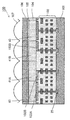
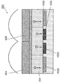
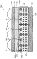
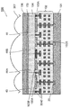
- FIG. 2A is a diagram showing a cross-sectional structure of the solid-state imaging device according to Embodiment 1.
- FIG. In the solid-state imaging device shown in the figure, a plurality of wiring layers 102 are formed on a semiconductor substrate 101. On the plurality of wiring layers 102, the first lower electrode 103A and the second lower electrode 103B are formed.
- a photoelectric conversion film 104 is formed on the first lower electrode 103 ⁇ / b> A and the second lower electrode 103 ⁇ / b> B, and a transparent upper electrode 105 is formed on the photoelectric conversion film 104.
- a color filter 106 is formed on the upper electrode 105, and a microlens 107 is formed on the color filter 106.
- the solid-state imaging device 100 includes a plurality of imaging pixels 40 and focus detection pixels 41A and 41B. That is, the solid-state imaging device 100 includes a plurality of imaging pixels and a pair of focus detection pixels.
- the imaging pixel 40 includes a wiring layer 102 formed on the semiconductor substrate 101, a first lower electrode 103A formed on the wiring layer 102, and a photoelectric conversion film formed on the first lower electrode 103A. 104 and an upper electrode 105 formed on the photoelectric conversion film 104. That is, the imaging pixel 40 has an imaging structure in which the photoelectric conversion film 104 is sandwiched between the upper electrode 105 and the first lower electrode 103A.
- the focus detection pixels 41A and 41B each include a wiring layer 102 formed on the semiconductor substrate 101 and a second lower electrode 103B formed on the wiring layer 102 and having a smaller area than the first lower electrode 103A.
- the second lower electrode 103B is eccentrically arranged in different directions from the pixel center. That is, each of the focus detection pixels 41A and 41B has a focus detection structure in which the photoelectric conversion film 104 is sandwiched between the second lower electrode 103B and the upper electrode 105 each having a smaller area than the first lower electrode 103A.
- the solid-state imaging device can use any material such as an organic material or an inorganic material with high efficiency for converting light into electric charge as a material used for the photoelectric conversion film 104.
- a photoelectric conversion film is formed of an organic material, it is possible to select an optimum material according to the wavelength band of incident light to be received. Therefore, the film thickness and shape of the photoelectric conversion film are adjusted for each pixel. There is no need. For this reason, it is not necessary to change the shape of the photoelectric conversion film, the surrounding microlens, the color filter, and the like corresponding to the wavelength band between the pixels.
- the solid-state imaging device it is not necessary to form a light-shielding band on the photoelectric conversion film 104 by using, for example, a metal material due to the structure of the focus detection pixels 41A and 41B. Therefore, there is no step on the photoelectric conversion film 104, so there is no need to change the shapes of the microlenses and color filters to be formed on the photoelectric conversion film 104, and the characteristics of the imaging pixels 40 are made uniform. It is possible to obtain a remarkable effect that the deterioration can be prevented and the focus detection can be performed with high accuracy.
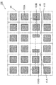
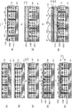
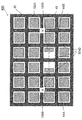
- FIG. 2B is a diagram illustrating a planar structure of the solid-state imaging device according to the first embodiment. This figure shows the planar structure of the first lower electrode 103A and the second lower electrode 103B. 2A is a cross-sectional view taken along the line XX in FIG. 2B. As shown in FIG. 2B, the solid-state imaging device 100 assigns a part of the imaging pixels 40 to the focus detection pixels 41A and 41B in the imaging area 35 in which a plurality of unit cells are arranged in a plane. It is the composition which is done. Further, two or more focus detection pixels are provided in the imaging region 35. However, the number of focus detection pixels is not limited to two (a pair), and may be three or more.
- the charges generated by the photoelectric conversion in the photoelectric conversion film 104 are collected on the first lower electrode 103A by applying an electric field between the upper electrode 105 and the first lower electrode 103A. Output as a pixel signal.
- the focus detection pixels 41A and 41B are each provided with a second lower electrode 103B, and each of the focus detection pixels 41A and 41B is connected to a separate charge detection node 25.
- the charges generated in the vicinity of the second lower electrode 103B are collected in the second lower electrode 103B according to the electric field and output as a focus detection signal.
- the charge generated in the region away from the second lower electrode 103B disappears before reaching the second lower electrode 103B due to recombination of electrons and holes, no signal is detected.
- the second lower electrode 103B is eccentrically arranged in different directions from the pixel center.
- the charge amount collected on the second lower electrode 103B of the focus detection pixel 41A and the charge amount collected on the second lower electrode 103B of the focus detection pixel 41B are, for example, from the same light source.
- the incident light can be made different, and focus detection can be performed based on the difference between these charge amounts.
- the solid-state imaging device 100 divides incident light into two light beams on the left and right sides to generate two divided images, detects a pattern shift between the two divided images, and determines the focus direction of the photographing lens.
- a so-called phase difference detection method for determining the amount of deviation from the focus position is employed.
- the solid-state imaging device 200 according to this modification is different from the first lower electrode 103A and the second lower electrode 103B in the focus detection pixels 42A and 42B as compared to the solid-state imaging device 100 according to the first embodiment.
- the configuration differs in that the third lower electrode 103C is formed.
- the configuration of the solid-state imaging device 200 will be described focusing on differences from the solid-state imaging device 100.
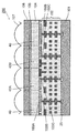
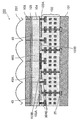
- FIG. 3A is a diagram showing a cross-sectional structure of a solid-state imaging device according to a modification of the first embodiment.
- a wiring layer 102 is formed on a semiconductor substrate 101, and a first lower electrode 103A, a second lower electrode 103B, and a third lower electrode 103C are formed thereon.
- a photoelectric conversion film 104 is formed so as to straddle over the first lower electrode 103A, the second lower electrode 103B, and the third lower electrode 103C.
- a transparent upper electrode 105 is formed on the photoelectric conversion film 104.
- the solid-state imaging device 200 according to this modification includes a plurality of imaging pixels 40 and focus detection pixels 42A and 42B. That is, the solid-state imaging device 200 includes a plurality of imaging pixels and a pair of focus detection pixels.
- the imaging pixel 40 has an imaging structure in which the photoelectric conversion film 104 is sandwiched between the upper electrode 105 and the first lower electrode 103A.
- the focus detection pixel 42A has a focus detection structure in which the photoelectric conversion film 104 is sandwiched between the second lower electrode 103B, the third lower electrode 103C, and the upper electrode 105.
- the second lower electrode 103B has a smaller area than the first lower electrode 103A.
- the third lower electrode 103C is connected to the power supply or grounded via the wiring layer 102.
- each of the focus detection pixels 42A and 42B according to the present modified example has a third lower electrode 103C connected to the power source or grounded via the wiring layer 102 in addition to the second lower electrode 103B. It is provided between the layer 102 and the photoelectric conversion film 104.
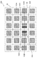
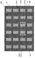
- FIG. 3B is a diagram illustrating a planar structure of the solid-state imaging device according to the modification of the first embodiment. Specifically, the drawing shows a planar structure of the first lower electrode 103A, the second lower electrode 103B, and the third lower electrode 103C.
- FIG. 3A is a YY cross-sectional view in FIG. 3B.
- FIG. 4 is a diagram showing the movement of charges photoelectrically converted by the focus detection pixels.
- a part of the imaging pixels 40 is assigned by replacing the focus detection pixels 42A and 42B in the imaging region 35 in which a plurality of unit cells are arranged in a plane. Two or more focus detection pixels are provided in the imaging region 35.
- the number of focus detection pixels is not limited to two (a pair), and may be three or more.
- the focus detection pixels 42A and 42B are provided with a second lower electrode 103B and a third lower electrode 103C, respectively, and are connected to separate wirings.
- the electric charges generated in the vicinity of the second lower electrode 103B are collected by the second lower electrode 103B according to the electric field and used as a focus detection signal.
- the electric charges generated in the vicinity of the third lower electrode 103C are collected by the third lower electrode 103C according to the electric field and discharged through the power supply wiring or the ground wiring.
- each of the second lower electrodes 103B collects charges in the vicinity thereof, so that the focus detection accuracy is improved.
- the focus detection pixels 42A and 42B are not necessarily adjacent to each other.
- the eccentric direction of the second lower electrode 103B from the pixel center is not limited to the above pattern.
- the second lower electrode 103B is decentered in the upper direction on the paper surface in FIGS. 2B and 3B, and in the focus detection pixel 42B, the second lower electrode 103B is deviated in the lower direction on the paper surface in FIGS. 2B and 3B. You may mind.
- FIG. 5 is a process cross-sectional view illustrating the method for manufacturing the solid-state imaging device according to the first embodiment.
- FIG. 5 shows a manufacturing process of the solid-state imaging device 200 according to the first modification of the present embodiment.
- the manufacturing method of the solid-state imaging device 100 according to the present embodiment is realized by omitting the formation process of the third lower electrode 103C from the manufacturing process shown in FIG.
- a plurality of signal readout circuits are formed on a semiconductor substrate 101, and a wiring layer 102 is formed on the semiconductor substrate 101.
- the process shown in FIG. 5A is performed using a known semiconductor manufacturing process.
- an insulating film 401 (for example, a silicon oxide film) is deposited on the wiring layer 102 by, for example, a plasma CVD (Chemical Vapor Deposition) method.
- the film thickness is 50 nm or more and 500 nm or less.
- the insulating film 401 is an interlayer insulating film between the uppermost layer of the wiring layer 102 and the lower electrode.
- a resist pattern is formed on the insulating film 401 by a lithography technique.
- the resist pattern is a pattern that opens a portion that electrically connects the uppermost layer of the wiring layer 102 and the lower electrode.
- anisotropic etching such as plasma etching is performed to form a connection portion between the uppermost layer of the wiring layer 102 and the lower electrode.
- a metal layer 402 for example, tungsten
- CMP Chemical Mechanical Polishing
- Flattening is performed.
- a metal layer 403 is deposited by a sputtering method or the like.
- the film thickness is 10 nm or more and 400 nm or less.
- the material of the metal layer 403 is, for example, copper, aluminum, titanium, tantalum, or the like.
- a resist pattern is formed on the metal layer 403 by lithography.
- the resist pattern is a pattern in which the resist remains in portions that become the first lower electrode 103A, the second lower electrode 103B, and the third lower electrode 103C.
- the first lower electrode 103A, the second lower electrode 103B, and the third lower electrode 103C are formed by anisotropic etching such as plasma etching. That is, the first lower electrode 103A, the second lower electrode 103B, and the third lower electrode 103C are formed of the same material in the same layer.
- the first lower electrode 103A is formed in the imaging region 140 on the wiring layer 102 where each of the plurality of imaging pixels 40 is formed.
- the focus detection regions 142A and 142B on the wiring layer 102 where the focus detection pixels 41A and 41B are respectively formed have a smaller area than the first lower electrode 103A and a pair of focus detection regions.
- the second lower electrode 103B is formed so as to be eccentrically arranged in different directions from the pixel center.
- an insulating film 404 (for example, a silicon oxide film) is deposited on the first lower electrode 103A, the second lower electrode 103B, and the third lower electrode 103C.
- planarization is performed by a CMP (Chemical Mechanical Polishing) method, and the first lower electrode 103A, the second lower electrode 103B, and the third lower electrode 103C are formed. Expose to the surface. At this time, the film thickness of the lower electrode is, for example, 50 nm to 200 nm.
- the photoelectric conversion film 104 is formed on the first lower electrode 103A, the second lower electrode 103B, and the third lower electrode 103C, and then the transparent upper electrode 105 is formed.
- the film thickness of the photoelectric conversion film 104 is, for example, 250 nm or more and 650 nm or less
- the film thickness of the upper electrode 105 is, for example, 50 nm or less.
- the color filter 106 is formed on the upper electrode 105, and then the microlens 107 is formed.
- the solid-state imaging device 200 includes the focus detection pixels 42 ⁇ / b> A and 42 ⁇ / b> B, so that the focus detection signal by the phase difference detection method is formed without forming a light shielding band on the photoelectric conversion film 104. Can be obtained.
- the solid-state imaging devices 100 and 200 according to the present embodiment can also prevent the characteristic deterioration and the reliability deterioration.
- the solid-state imaging devices 100 and 200 according to the present embodiment or the manufacturing methods thereof, even the solid-state imaging device including the photoelectric conversion film 104 can perform focus detection with high accuracy.
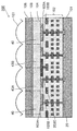
- FIG. 6A is a diagram illustrating a cross-sectional structure of the solid-state imaging device according to the second embodiment
- FIG. 6B is a diagram illustrating a planar structure of the solid-state imaging device according to the second embodiment.
- 6A is a ZZ cross-sectional view in FIG. 6B.
- the solid-state imaging device 300 according to the present embodiment differs from the solid-state imaging device 100 according to the first embodiment in the configuration of the third lower electrode provided in the adjacent focus detection pixels 43A and 43B.
- electric charges generated by photoelectric conversion in the photoelectric conversion film 104 are applied by applying an electric field between the upper electrode 105, the second lower electrode 103B, and the third lower electrode 203C. Collected to the second lower electrode 103B or the third lower electrode 203C and output as an electrical signal. The charges generated in the vicinity of the second lower electrode 103B are collected in the second lower electrode 103B in accordance with the electric field, and the charges generated in the vicinity of the third lower electrode 203C are in the third in accordance with the electric field. The lower electrode 203C is collected. The electric charge collected at the second lower electrode 103B is used as a focus detection signal, and the electric charge collected at the third lower electrode 203C is discharged by being connected or grounded to the power supply wiring.
- one third lower electrode 203C is shared between adjacent focus detection pixels 43A and 43B. This simplifies the layout and reduces the number of wires and the number of power supplies. Therefore, it is possible to improve the operation speed and reduce the defect rate.
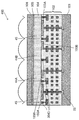
- FIG. 7A is a diagram illustrating a cross-sectional structure of the solid-state imaging device according to Embodiment 3
- FIG. 7B is a diagram illustrating a planar structure of the solid-state imaging device according to Embodiment 3.
- 7A is a cross-sectional view taken along the line VV in FIG. 7B.
- the solid-state imaging device according to the present embodiment is different from the solid-state imaging device according to the first embodiment in that a fourth lower electrode 304D that is common to all the pixels arranged in the imaging region 35 is connected. .
- the fourth lower electrode 304D is between adjacent lower electrodes of the plurality of first lower electrodes 103A and the plurality of second lower electrodes 103B, and is the first lower electrode 103A and the second lower electrode. It is a lower electrode different from 103B.
- the fourth lower electrode 304D is disposed between the plurality of first lower electrodes 103A and the plurality of second lower electrodes 103B so as to extend at least in the row direction or the column direction.
- the fourth lower electrode 304 ⁇ / b> D is a shield electrode that is connected to the power supply or grounded via the wiring layer 102.
- the layout is simplified, the number of wirings and the number of power supplies can be reduced, and the defect rate can be reduced. realizable.
- the first lower electrode 103A and the second lower electrode 103B of each pixel are disposed so as to be surrounded by the fourth lower electrode 304D, whereby the first lower electrode of the adjacent pixel is arranged.
- Capacitive coupling between 103A and the second lower electrode 103B can be suppressed.
- the influence of the signal level of adjacent pixels can be greatly reduced.
- the fourth lower electrode 304D not only suppresses capacitive coupling but also has a function of extracting charges in the vicinity of the fourth lower electrode 304D. That is, by discharging charges generated between adjacent pixels, an effect of suppressing optical crosstalk that occurs until incident light reaches the photoelectric conversion film can also be obtained.
- FIGS. 8A and 8B a modification of the present embodiment will be described based on FIGS. 8A and 8B.
- the solid-state imaging device 500 according to this modification is different from the second lower electrode 103B and the second lower electrode 103B in the focus detection pixels 46A and 46B as compared with the solid-state imaging device 400 according to the third embodiment.
- the structure is different in that another lower electrode is formed.
- the configuration of the solid-state imaging device 500 will be described focusing on differences from the solid-state imaging device 400.
- FIG. 8A is a diagram illustrating a cross-sectional structure of a solid-state imaging device according to a modification of the third embodiment
- FIG. 8B is a diagram illustrating a planar structure of the solid-state imaging device according to the modification of the third embodiment.
- 8A is a cross-sectional view taken along the line WW in FIG. 8B.
- the fourth lower electrode 305D common to all the pixels arranged in the imaging region 35 is connected, similarly to the solid-state imaging device 500 according to the third embodiment.
- the fourth lower electrode 305D is arranged in a grid pattern in the boundary region between the imaging pixel 45 and the focus detection pixels 46A and 46B.
- the fourth lower electrode 305D is formed so as to extend at least in the row direction or the column direction between the plurality of first lower electrodes 103A and the plurality of second lower electrodes 103B.
- the fourth lower electrode 305 ⁇ / b> D is a shield electrode that is power-connected or grounded via the wiring layer 102.
- the fourth lower electrode 305D is also arranged in a region where the second lower electrode 103B is not formed in the focus detection pixels 46A and 46B. That is, in the solid-state imaging device 500 according to the present modification, the third lower electrode 103C in the solid-state imaging device 200 according to the modification of the first embodiment and the fourth lower portion in the solid-state imaging device 400 according to the third embodiment.
- the electrode 304D is continuously formed without being separated. As a result, the fourth lower electrode 305D is formed, and capacitive coupling between adjacent pixels can be suppressed, and the discharge of unnecessary charges in the focus detection pixels 46A and 46B is enhanced.
- FIG. 9 is a diagram illustrating a planar structure of the solid-state imaging device according to the fourth embodiment.
- the solid-state imaging device includes a first lower electrode arranged in the imaging pixel 47 in the focus detection pixels 48A and 48B.
- the structure is different in that 203A is provided.
- the focus detection pixels 48A and 48B realize an imaging and focus detection pixel having both functions of the imaging pixel and the focus detection pixel. In other words, some of the plurality of imaging pixels 47 have a focus detection function.
- the solid-state imaging device 600 includes a plurality of imaging pixels 47 and focus detection pixels 48A and 48B. That is, the solid-state imaging device 600 includes a plurality of imaging pixels and a plurality of focus detection pixels.
- the imaging pixel 47 has an imaging structure in which the photoelectric conversion film 104 is sandwiched between the upper electrode 105 and the first lower electrode 203A.
- the photoelectric conversion film 104 is sandwiched between the first lower electrode 203A and the second lower electrode 203B having a smaller area than the first lower electrode 203A and the upper electrode 105, respectively.
- Structure and focus detection structure That is, the focus detection pixels 48 ⁇ / b> A and 48 ⁇ / b> B include the second lower electrode 203 ⁇ / b> B formed between the wiring layer 102 and the photoelectric conversion film 104, and further formed between the wiring layer 102 and the photoelectric conversion film 104.
- the first lower electrode 203A is provided.
- the fourth lower electrode 203D is arranged in a grid pattern in the boundary region between the imaging pixel 47 and the focus detection pixels 48A and 48B.
- the fourth lower electrode 203 ⁇ / b> D is a shield electrode that is connected to the power source or grounded via the wiring layer 102.
- the missing pixels are corrected by performing image processing by complementing using the signal information of the imaging pixels.
- the focus detection pixel can be configured so that the imaging function is not lost while maintaining the focus detection function, so that the focus that does not require image correction can be obtained.
- a solid-state imaging device having a detection function can be realized.
- FIG. 10 is a diagram showing a cross-sectional structure of the solid-state imaging device according to the fifth embodiment.
- the solid-state imaging device 700 according to the present embodiment is different from the solid-state imaging devices according to the first to fourth embodiments in that the center of the microlens 207 on the focus detection pixels 46A and 46B is the corresponding focus detection pixel 46A. And the center of 46B is different in that each second lower electrode 103B is deviated in an eccentric direction. By doing so, the amount of charge generated in the photoelectric conversion film in the focus detection pixel is biased. In the present embodiment, the amount of charge in the vicinity of the second lower electrode 103B is reduced. As a result, since the focus detection signals received by the left and right focus detection pixels 46A and 46B can be controlled with higher accuracy, the focus detection accuracy can be improved.
- the microlens 207 can be formed by performing lithography using, for example, a gray scale mask (photomask) having different light transmittances depending on positions.
- a gray scale mask photomask
- FIG. 11 is a diagram showing a cross-sectional structure of the solid-state imaging device according to the sixth embodiment.
- the solid-state imaging device 800 according to the present embodiment is different from the solid-state imaging devices according to the first to fourth embodiments in that the microlenses 307 on the adjacent focus detection pixels 46A and 46B are shared.
- the microlens on the focus detection pixel has an asymmetrical configuration, so that the focus detection accuracy is improved as in the fifth embodiment. Can be realized.
- the dimension controllability (dimension uniformity in the imaging region) is excellent.
- a gray scale mask it is not necessary to use a gray scale mask, that is, improvement in focus detection accuracy can be realized by a low-cost manufacturing method using a general photomask.
- a gray scale mask can be used to further optimize the shape of the microlens.
- one aspect of the solid-state imaging device is a solid-state imaging device having an imaging region in which a plurality of pixels are arranged, and the plurality of pixels includes a plurality of imaging pixels 40 and a plurality of pixels.
- Each of the plurality of imaging pixels 40 includes a first lower electrode 103A, a photoelectric conversion film 104 formed on the first lower electrode 103A, and a photoelectric conversion.
- the film 104 and the upper electrode 105 formed on the photoelectric conversion film 104 are provided, the second lower electrode 103B has a smaller area than the first lower electrode 103A, and the focus detection pixels 41A and 41B include The second lower electrode 103B of respectively, are arranged eccentrically in different directions from the pixel center.
- the first lower electrode and the second lower electrode are formed in the same layer. Thereby, the surface of the photoelectric conversion film can be further planarized.
- each of the focus detection pixels 42A and 42B includes a third lower electrode 103C different from the second lower electrode 103B, and the third lower electrode 103C may be connected to a power source or grounded. .
- each of the second lower electrodes 103B collects charges in the vicinity thereof, so that the focus detection accuracy is improved.
- the plurality of focus detection pixels 43A and 43B may share the third lower electrode 203C.
- a fourth lower electrode 304D different from the first lower electrode 103A and the second lower electrode 103B formed between the adjacent first lower electrode 103A and the second lower electrode 103B is provided. May be.
- the third lower electrode and the fourth lower electrode 305D may be formed continuously.
- each of the focus detection pixels 48A and 48B may include the first lower electrode 203A.
- a microlens is provided on each of the focus detection pixels 46A and 46B, and the center of each microlens is decentered from the center of the corresponding focus detection pixel. It may be displaced in the direction.
- one shared microlens may be disposed on the adjacent focus detection pixels 46A and 46B.
- the photoelectric conversion film 104 may be made of an organic material.
- one aspect of the method for manufacturing the solid-state imaging device according to the above embodiment is a solid-state imaging device having an imaging region in which a plurality of imaging pixels 40 and a plurality of focus detection pixels 42A and 42B are arranged in a matrix.
- the first lower electrode in the step of forming the wiring layer 102 on the semiconductor substrate and the imaging region 140 on the wiring layer 102 where each of the plurality of imaging pixels 40 is formed.
- the area is smaller than that of the first lower electrode 103A, and A step of forming the second lower electrode 103B so as to be eccentrically arranged in different directions from the pixel center, and the first lower electrode 103A and the second lower electrode 1 On 3B, and forming the photoelectric conversion layer 104, and forming an upper electrode 105 on the photoelectric conversion film 104.
- two or more focus detection pixels may be provided in the imaging region 35, and may not be adjacent to each other as in the first to sixth embodiments.
- the number and position of the focus detection pixels are determined by the required performance and specifications of the solid-state imaging device.
- the solid-state imaging device can provide a high-speed and high-accuracy phase difference detection autofocus function without deterioration in image quality, and is particularly effective for a digital camera or the like.
Abstract
A solid state image-capture device (100) is constituted from a plurality of image-capture pixels (40) and a plurality of focal point detection pixels (41A and 41B). Each image-capture pixel (40) is provided with a first lower part electrode (103A), a photoelectric conversion film (104) formed above the first lower part electrode (103A), and an upper part electrode (105) formed above the photoelectric conversion film (104). The focal point detection pixels (41A and 41B) are each provided with a second lower part electrode (103B), the photoelectric conversion film (104) formed above the second lower part electrode (103B), and the upper part electrode (105) formed above the photoelectric conversion film (104). The second lower part electrodes have a smaller surface area than the first lower part electrode, the respective second lower part electrodes (103B) being disposed off-centered from the pixel center in different directions from each other in the two focal point detection pixels (41A and 41B) contained in the plurality of focal point detection pixels.
Description
本開示は、固体撮像装置に関する。
The present disclosure relates to a solid-state imaging device.
カメラセットの小型化とフォーカス速度の向上のために、焦点検出機能を持つ固体撮像装置が提案されており、焦点検出方式の一つとして位相差検出方式が知られている。
In order to reduce the size of the camera set and improve the focus speed, a solid-state imaging device having a focus detection function has been proposed, and a phase difference detection method is known as one of focus detection methods.
特許文献1および2に示された固体撮像装置では受光部(フォトダイオード)の半分程度を、金属材料等により形成された遮光帯により遮光し、それにより位相差検出を行う方式が開示されている。
In the solid-state imaging devices disclosed in Patent Documents 1 and 2, a method is disclosed in which about half of the light receiving portion (photodiode) is shielded by a shading band formed of a metal material or the like, thereby detecting a phase difference. .
光電変換膜を備える固体撮像装置に、背景技術と同じように、位相差検出方式を行うための画素(焦点検出用画素)として光電変換膜(受光部)の上に遮光帯を形成すると、焦点検出用画素の周辺で光電変換膜上に段差が生じる。このため、焦点検出用画素周辺のカラーフィルタおよびマイクロレンズの形成が不均一となり、画質特性が悪化する。
When a light-shielding band is formed on a photoelectric conversion film (light receiving unit) as a pixel (focus detection pixel) for performing a phase difference detection method on a solid-state imaging device including a photoelectric conversion film, as in the background art, A step is formed on the photoelectric conversion film around the detection pixel. For this reason, the formation of color filters and microlenses around the focus detection pixels becomes non-uniform, and image quality characteristics deteriorate.
本開示は、画質の劣化を抑制しつつ、高精度の焦点検出用画素を搭載した固体撮像装置およびその製造方法を提供する。
The present disclosure provides a solid-state imaging device equipped with high-precision focus detection pixels while suppressing deterioration in image quality, and a method for manufacturing the same.
本開示の一態様に係る固体撮像装置は、複数の画素が配置された撮像領域を有する固体撮像装置であって、前記複数の画素は、複数の撮像用画素と複数の焦点検出用画素とを含み、前記複数の撮像用画素のそれぞれは、第1の下部電極と、前記第1の下部電極の上に形成された光電変換膜と、前記光電変換膜の上に形成された上部電極とを備え、前記複数の焦点検出用画素のそれぞれは、第2の下部電極と、前記第2の下部電極の上に形成された前記光電変換膜と、前記光電変換膜の上に形成された上部電極とを備え、前記第2の下部電極は、前記第1の下部電極よりも面積が小さく、前記複数の焦点検出用画素に含まれる2つの焦点検出用画素は、それぞれの第2の下部電極が、画素中心から互いに異なる方向に偏心して配置されていることを特徴とする。
A solid-state imaging device according to an aspect of the present disclosure is a solid-state imaging device having an imaging region in which a plurality of pixels are arranged, and the plurality of pixels includes a plurality of imaging pixels and a plurality of focus detection pixels. Each of the plurality of imaging pixels includes a first lower electrode, a photoelectric conversion film formed on the first lower electrode, and an upper electrode formed on the photoelectric conversion film. Each of the plurality of focus detection pixels includes a second lower electrode, the photoelectric conversion film formed on the second lower electrode, and an upper electrode formed on the photoelectric conversion film And the second lower electrode has a smaller area than the first lower electrode, and the two lower detection electrodes included in the plurality of focus detection pixels have respective second lower electrodes. Are arranged eccentrically in different directions from the pixel center. And wherein the door.
本開示によれば、画質の劣化を抑制しつつ、高精度の焦点検出用画素を搭載した固体撮像装置を提供することが可能となる。
According to the present disclosure, it is possible to provide a solid-state imaging device equipped with high-precision focus detection pixels while suppressing deterioration in image quality.
(本開示の基礎となった知見)
本開示にかかる固体撮像装置の実施の形態を説明する前に、本開示の基礎となった知見について説明する。 (Knowledge that became the basis of this disclosure)
Prior to describing an embodiment of a solid-state imaging device according to the present disclosure, knowledge that is the basis of the present disclosure will be described.
本開示にかかる固体撮像装置の実施の形態を説明する前に、本開示の基礎となった知見について説明する。 (Knowledge that became the basis of this disclosure)
Prior to describing an embodiment of a solid-state imaging device according to the present disclosure, knowledge that is the basis of the present disclosure will be described.
イメージセンサの画素サイズは、最新の微細加工技術を用いてもなお、受光部(フォトダイオード)に利用可能なスペースは限られている。画素面積のほとんどが、駆動回路のために必要とされる電子部品(電界効果トランジスタなど)によって占有されている為である。
The space available for the light receiving part (photodiode) is limited even if the pixel size of the image sensor uses the latest fine processing technology. This is because most of the pixel area is occupied by electronic components (such as field effect transistors) required for the drive circuit.
この問題を解決するため、シリコン基板上に受光部を設けるのではなく、光電変換膜を、有機材料などを用いて上層に配置した固体撮像装置が提案されている。
In order to solve this problem, there has been proposed a solid-state imaging device in which a photoelectric conversion film is disposed in an upper layer using an organic material or the like instead of providing a light receiving portion on a silicon substrate.
しかしながら、上層に光電変換膜を備える固体撮像装置に位相差検出方式を適用しようとした場合、従来技術と同じように、焦点検出用画素として光電変換膜(受光部)の上に遮光帯を形成すると、焦点検出用画素の周辺で光電変換膜上に段差が生じることになる。このため、光電変換膜の上に形成されるカラーフィルタおよびマイクロレンズの形成が不均一となり、画質特性が悪化する。従って、上層に光電変換膜を備える固体撮像装置にあっては、画質特性の悪化を抑制しつつ位相差検出方式を実現可能な技術が求められている。
However, when the phase difference detection method is applied to a solid-state imaging device having a photoelectric conversion film on the upper layer, a light-shielding band is formed on the photoelectric conversion film (light receiving unit) as a focus detection pixel, as in the prior art. Then, a step is generated on the photoelectric conversion film around the focus detection pixel. For this reason, the color filters and microlenses formed on the photoelectric conversion film are not uniformly formed, and the image quality characteristics are deteriorated. Therefore, for a solid-state imaging device having a photoelectric conversion film as an upper layer, a technique capable of realizing a phase difference detection method while suppressing deterioration in image quality characteristics is required.
以下、図面を参照しながら、本実施の形態に係る固体撮像装置の詳細を説明する。なお、以下の実施の形態は、いずれも本開示の一具体例を示すものであり、数値、形状、材料、構成要素、構成要素の配置位置および接続形態などは、一例であり、本開示を限定するものではない。
Hereinafter, details of the solid-state imaging device according to the present embodiment will be described with reference to the drawings. Note that each of the following embodiments is a specific example of the present disclosure, and numerical values, shapes, materials, components, arrangement positions and connection forms of the components are examples, and the present disclosure is not limited. It is not limited.
(実施の形態1)
[1.回路構成]
図1は、実施の形態1に係る固体撮像装置の回路構成を示す図である。 (Embodiment 1)
[1. Circuit configuration]
FIG. 1 is a diagram illustrating a circuit configuration of the solid-state imaging device according to the first embodiment.
[1.回路構成]
図1は、実施の形態1に係る固体撮像装置の回路構成を示す図である。 (Embodiment 1)
[1. Circuit configuration]
FIG. 1 is a diagram illustrating a circuit configuration of the solid-state imaging device according to the first embodiment.
本実施の形態に係る固体撮像装置100は、行列状に単位セル20が配置された撮像領域を有する。図1に記載された単位セル20は、増幅トランジスタ21と、リセットトランジスタ22と、アドレストランジスタ23と、入射光を受ける画素である光電変換素子24(後述する図2における光電変換膜104)と、これらを結線する配線(金属配線)とで構成された繰り返し単位となるセルであり、入射光に応じた画素信号を生成する。
The solid-state imaging device 100 according to the present embodiment has an imaging region in which unit cells 20 are arranged in a matrix. 1 includes an amplification transistor 21, a reset transistor 22, an address transistor 23, a photoelectric conversion element 24 (a photoelectric conversion film 104 in FIG. 2 described later) that is a pixel that receives incident light, This is a cell that is a repeating unit composed of wiring (metal wiring) that connects these, and generates a pixel signal corresponding to incident light.
また、単位セル20の光電変換素子24(後述する図2における光電変換膜104)は、後述する図(図2等)に示すように、画像撮像を行う画素(撮像用画素40)と、オートフォーカスなどの焦点を検知するための画素(焦点検出用画素41A、41B)とが含まれる。焦点を検出するための画素とは、具体的には、結像した2つの画像の間隔からピントの方向と量を判断するための画素である。
In addition, the photoelectric conversion element 24 (photoelectric conversion film 104 in FIG. 2 described later) of the unit cell 20 includes a pixel (imaging pixel 40) that performs image capturing and an auto as shown in a diagram (FIG. 2 and the like) described later. Pixels for detecting a focus such as a focus ( focus detection pixels 41A and 41B) are included. Specifically, the pixel for detecting the focal point is a pixel for determining the focus direction and amount from the interval between the two images formed.
増幅トランジスタ21のソースには、垂直方向に走る電源配線27が接続されている。リセットトランジスタ22のゲートには、水平方向に走るリセット信号線28が接続され、ソースには垂直方向に走るフィードバック信号線30が接続されている。アドレストランジスタ23のゲートには、水平方向に走るアドレス信号線29が接続され、ドレインには垂直方向に走る垂直信号線26が接続されている。
The power source wiring 27 running in the vertical direction is connected to the source of the amplification transistor 21. A reset signal line 28 running in the horizontal direction is connected to the gate of the reset transistor 22, and a feedback signal line 30 running in the vertical direction is connected to the source. An address signal line 29 running in the horizontal direction is connected to the gate of the address transistor 23, and a vertical signal line 26 running in the vertical direction is connected to the drain.
垂直信号線26は、列毎に配置され、画素信号を周辺回路へ伝達する主信号線である。電源配線27は、列毎に配置され、対応する列に属する単位セル20に電源電圧を供給する。フィードバック信号線30は、列毎に配置され、周辺回路からのフィードバック信号を対応する列に属する単位セル20に伝達する。
The vertical signal line 26 is a main signal line that is arranged for each column and transmits a pixel signal to a peripheral circuit. The power supply wiring 27 is arranged for each column and supplies a power supply voltage to the unit cells 20 belonging to the corresponding column. The feedback signal line 30 is arranged for each column, and transmits the feedback signal from the peripheral circuit to the unit cells 20 belonging to the corresponding column.
単位セル20内の光電変換素子24で生成された信号電荷は、電荷蓄積ノード25で電圧に変換され、増幅トランジスタ21で増幅され、画素信号として垂直信号線26に出力される。画素信号が読み出された後、電荷蓄積ノード25に蓄積された電荷はリセットされる。ここで、リセット後に残存するランダムノイズの乗った蓄積電荷を打ち消すために、フィードバック信号線30とフィードバックアンプ31とが1対1で配置されている。フィードバックアンプ31の負入力端子には垂直信号線26が接続され、フィードバックアンプ31の出力端子には、スイッチを介してフィードバック信号線30が接続されている。
The signal charge generated by the photoelectric conversion element 24 in the unit cell 20 is converted into a voltage by the charge storage node 25, amplified by the amplification transistor 21, and output to the vertical signal line 26 as a pixel signal. After the pixel signal is read, the charge accumulated in the charge accumulation node 25 is reset. Here, the feedback signal line 30 and the feedback amplifier 31 are arranged on a one-to-one basis in order to cancel the accumulated charge with random noise remaining after the reset. The vertical signal line 26 is connected to the negative input terminal of the feedback amplifier 31, and the feedback signal line 30 is connected to the output terminal of the feedback amplifier 31 via a switch.
上記構成において、電荷蓄積ノード25に蓄積された電荷がリセットトランジスタ22によりリセットされる際(リセットトランジスタ22が導通状態)、電荷蓄積ノード25に発生するランダムノイズは、増幅トランジスタ21、アドレストランジスタ23、垂直信号線26、周辺回路の一部であるフィードバックアンプ31およびフィードバック信号線30を介して、リセットトランジスタ22のソースに負帰還フィードバックされる。これにより、電荷蓄積ノード25のノイズ成分が打ち消され、ランダムノイズを低減することができる。
In the above configuration, when the charge accumulated in the charge accumulation node 25 is reset by the reset transistor 22 (the reset transistor 22 is in a conductive state), random noise generated in the charge accumulation node 25 is generated by the amplification transistor 21, the address transistor 23, Negative feedback is fed back to the source of the reset transistor 22 through the vertical signal line 26, the feedback amplifier 31 and the feedback signal line 30 which are part of the peripheral circuit. As a result, the noise component of the charge storage node 25 is canceled, and random noise can be reduced.
すなわち、信号電荷を転送またはリセットする際に、ランダムノイズが発生する。リセット時にランダムノイズが残存すると、次に蓄積される信号電荷は残存ノイズに加算される為、当該信号電荷を読み出す際に当該ランダムノイズが重畳された信号が出力されることになる。そこで、本実施の形態に係る固体撮像装置は、このランダムノイズを除去するためにフィードバック回路を備え、各単位セルから出力されたランダムノイズ信号を検知して、ランダムノイズが重畳された蓄積電荷を打ち消すように各単位セルへ信号をフィードバックさせている。
That is, random noise is generated when signal charges are transferred or reset. If random noise remains at the time of resetting, the signal charge to be accumulated next is added to the remaining noise. Therefore, when the signal charge is read, a signal on which the random noise is superimposed is output. Therefore, the solid-state imaging device according to the present embodiment includes a feedback circuit for removing the random noise, detects the random noise signal output from each unit cell, and stores the accumulated charge on which the random noise is superimposed. A signal is fed back to each unit cell so as to cancel.
[2.画素構成]
図2Aは、実施の形態1に係る固体撮像装置の断面構造を示す図である。同図に示された固体撮像装置は、半導体基板101上に複数の配線層102が形成されている。複数の配線層102上に、第1の下部電極103Aおよび第2の下部電極103Bが形成されている。第1の下部電極103Aおよび第2の下部電極103Bの上に、光電変換膜104が形成され、光電変換膜104上に、透明な上部電極105が形成されている。また、上部電極105上に、カラーフィルタ106が形成され、カラーフィルタ106上に、マイクロレンズ107が形成されている。 [2. Pixel configuration]
2A is a diagram showing a cross-sectional structure of the solid-state imaging device according toEmbodiment 1. FIG. In the solid-state imaging device shown in the figure, a plurality of wiring layers 102 are formed on a semiconductor substrate 101. On the plurality of wiring layers 102, the first lower electrode 103A and the second lower electrode 103B are formed. A photoelectric conversion film 104 is formed on the first lower electrode 103 </ b> A and the second lower electrode 103 </ b> B, and a transparent upper electrode 105 is formed on the photoelectric conversion film 104. A color filter 106 is formed on the upper electrode 105, and a microlens 107 is formed on the color filter 106.
図2Aは、実施の形態1に係る固体撮像装置の断面構造を示す図である。同図に示された固体撮像装置は、半導体基板101上に複数の配線層102が形成されている。複数の配線層102上に、第1の下部電極103Aおよび第2の下部電極103Bが形成されている。第1の下部電極103Aおよび第2の下部電極103Bの上に、光電変換膜104が形成され、光電変換膜104上に、透明な上部電極105が形成されている。また、上部電極105上に、カラーフィルタ106が形成され、カラーフィルタ106上に、マイクロレンズ107が形成されている。 [2. Pixel configuration]
2A is a diagram showing a cross-sectional structure of the solid-state imaging device according to
本実施の形態に係る固体撮像装置100は、複数の撮像用画素40と焦点検出用画素41Aおよび41Bとを有する。つまり、固体撮像装置100は、複数の撮像用画素と一対の焦点検出用画素とで構成される。
The solid-state imaging device 100 according to the present embodiment includes a plurality of imaging pixels 40 and focus detection pixels 41A and 41B. That is, the solid-state imaging device 100 includes a plurality of imaging pixels and a pair of focus detection pixels.
撮像用画素40は、半導体基板101上に形成された配線層102と、配線層102上に形成された第1の下部電極103Aと、第1の下部電極103Aの上に形成された光電変換膜104と、光電変換膜104の上に形成された上部電極105とを備える。つまり、撮像用画素40は、上部電極105と第1の下部電極103Aとで光電変換膜104が挟まれた撮像構造を有する。
The imaging pixel 40 includes a wiring layer 102 formed on the semiconductor substrate 101, a first lower electrode 103A formed on the wiring layer 102, and a photoelectric conversion film formed on the first lower electrode 103A. 104 and an upper electrode 105 formed on the photoelectric conversion film 104. That is, the imaging pixel 40 has an imaging structure in which the photoelectric conversion film 104 is sandwiched between the upper electrode 105 and the first lower electrode 103A.
焦点検出用画素41Aおよび41Bは、それぞれ、半導体基板101上に形成された配線層102と、配線層102上に形成された、第1の下部電極103Aよりも面積の小さい第2の下部電極103Bと、第2の下部電極103Bの上に形成された光電変換膜104と、光電変換膜104の上に形成された上部電極105とを備える。さらに、焦点検出用画素である一対の焦点検出用画素41Aおよび41Bでは、撮像領域を平面視した場合、第2の下部電極103Bが画素中心から互いに異なる方向に偏心して配置されている。つまり、焦点検出用画素41Aおよび41Bは、それぞれ、第1の下部電極103Aよりも面積の小さい第2の下部電極103Bと上部電極105とで光電変換膜104が挟まれた焦点検出構造を有する。
The focus detection pixels 41A and 41B each include a wiring layer 102 formed on the semiconductor substrate 101 and a second lower electrode 103B formed on the wiring layer 102 and having a smaller area than the first lower electrode 103A. A photoelectric conversion film 104 formed on the second lower electrode 103B, and an upper electrode 105 formed on the photoelectric conversion film 104. Further, in the pair of focus detection pixels 41A and 41B, which are focus detection pixels, when the imaging region is viewed in plan, the second lower electrode 103B is eccentrically arranged in different directions from the pixel center. That is, each of the focus detection pixels 41A and 41B has a focus detection structure in which the photoelectric conversion film 104 is sandwiched between the second lower electrode 103B and the upper electrode 105 each having a smaller area than the first lower electrode 103A.
また、本実施の形態に係る固体撮像装置は、光電変換膜104に用いる材料として、光から電荷へ変換する効率が高い有機材料または無機材料など、あらゆる材料を用いることができる。特に、有機材料により光電変換膜を形成した場合、受光すべき入射光の波長帯域に応じて最適材料を選択することが可能であるため、光電変換膜の膜厚や形状を画素ごとに調整する必要がない。このため、画素間で、波長帯域に対応させて光電変換膜およびその周辺のマイクロレンズおよびカラーフィルタなどの形状を変化させる必要がない。
In addition, the solid-state imaging device according to this embodiment can use any material such as an organic material or an inorganic material with high efficiency for converting light into electric charge as a material used for the photoelectric conversion film 104. In particular, when a photoelectric conversion film is formed of an organic material, it is possible to select an optimum material according to the wavelength band of incident light to be received. Therefore, the film thickness and shape of the photoelectric conversion film are adjusted for each pixel. There is no need. For this reason, it is not necessary to change the shape of the photoelectric conversion film, the surrounding microlens, the color filter, and the like corresponding to the wavelength band between the pixels.
本実施の形態に係る固体撮像装置は、焦点検出用画素41Aおよび41Bの構造により、光電変換膜104の上に、例えば金属材料により遮光帯を形成する必要がない。そのため、光電変換膜104上に段差が生じないので、光電変換膜104の上に形成すべきマイクロレンズおよびカラーフィルタなどの形状を変化させる必要がなく、撮像用画素40の特性を均一にして画質劣化を防ぎ、かつ、焦点検出を高精度に実施できるという顕著な効果を得ることが可能となる。
In the solid-state imaging device according to the present embodiment, it is not necessary to form a light-shielding band on the photoelectric conversion film 104 by using, for example, a metal material due to the structure of the focus detection pixels 41A and 41B. Therefore, there is no step on the photoelectric conversion film 104, so there is no need to change the shapes of the microlenses and color filters to be formed on the photoelectric conversion film 104, and the characteristics of the imaging pixels 40 are made uniform. It is possible to obtain a remarkable effect that the deterioration can be prevented and the focus detection can be performed with high accuracy.
図2Bは、実施の形態1に係る固体撮像装置の平面構造を示す図である。同図には、第1の下部電極103Aおよび第2の下部電極103Bの平面構造が示されている。なお、図2Aは、図2BにおけるX-X断面図である。図2Bに示すように、固体撮像装置100は、複数の単位セルが平面状に配置された撮像領域35のなかで、撮像用画素40の一部が焦点検出用画素41Aおよび41Bに置き換えて割り当てられている構成である。また、焦点検出用画素は、撮像領域35内に2箇所以上設けられるが2箇所(一対)に限定するものではなく3箇所以上設けても良い。
FIG. 2B is a diagram illustrating a planar structure of the solid-state imaging device according to the first embodiment. This figure shows the planar structure of the first lower electrode 103A and the second lower electrode 103B. 2A is a cross-sectional view taken along the line XX in FIG. 2B. As shown in FIG. 2B, the solid-state imaging device 100 assigns a part of the imaging pixels 40 to the focus detection pixels 41A and 41B in the imaging area 35 in which a plurality of unit cells are arranged in a plane. It is the composition which is done. Further, two or more focus detection pixels are provided in the imaging region 35. However, the number of focus detection pixels is not limited to two (a pair), and may be three or more.
撮像用画素40において、光電変換膜104中で光電変換により発生した電荷は、上部電極105と第1の下部電極103Aとの間に電界をかけることによって、第1の下部電極103Aへ集められ、画素信号として出力される。
In the imaging pixel 40, the charges generated by the photoelectric conversion in the photoelectric conversion film 104 are collected on the first lower electrode 103A by applying an electric field between the upper electrode 105 and the first lower electrode 103A. Output as a pixel signal.
焦点検出用画素41Aおよび41Bでは、それぞれ、第2の下部電極103Bが設けられ、それぞれの焦点検出用画素41Aおよび41Bは、別々の電荷検出ノード25に接続される。焦点検出用画素41Aおよび41Bにおいて、第2の下部電極103Bの近傍で発生した電荷は、電界に応じて、第2の下部電極103Bに集められ、焦点検出用信号として出力される。一方、第2の下部電極103Bから離れた領域で発生した電荷は、電子・ホールの再結合により第2の下部電極103Bに到達する前に消滅するため、信号検出されない。
The focus detection pixels 41A and 41B are each provided with a second lower electrode 103B, and each of the focus detection pixels 41A and 41B is connected to a separate charge detection node 25. In the focus detection pixels 41A and 41B, the charges generated in the vicinity of the second lower electrode 103B are collected in the second lower electrode 103B according to the electric field and output as a focus detection signal. On the other hand, since the charge generated in the region away from the second lower electrode 103B disappears before reaching the second lower electrode 103B due to recombination of electrons and holes, no signal is detected.
ここで、焦点検出用画素41Aおよび41Bでは、撮像領域を平面視した場合、第2の下部電極103Bが画素中心から互いに異なる方向に偏心して配置されている。これにより、焦点検出用画素41Aの第2の下部電極103Bに集められた電荷量と、焦点検出用画素41Bの第2の下部電極103Bに集められた電荷量とを、例えば、同一光源からの入射光に対して異ならせることが可能となり、これらの電荷量の差分に基づいて、焦点検出をすることが可能となる。
Here, in the focus detection pixels 41A and 41B, when the imaging region is viewed in plan, the second lower electrode 103B is eccentrically arranged in different directions from the pixel center. As a result, the charge amount collected on the second lower electrode 103B of the focus detection pixel 41A and the charge amount collected on the second lower electrode 103B of the focus detection pixel 41B are, for example, from the same light source. The incident light can be made different, and focus detection can be performed based on the difference between these charge amounts.
つまり、本実施の形態に係る固体撮像装置100は、入射光を左右2つの光に分けて2つの分割像を生成し、その2つの分割像のパターンずれを検出して撮影レンズのピント方向とフォーカス位置からのずれ量を判断する、いわゆる位相差検知方式が採用される。
In other words, the solid-state imaging device 100 according to the present embodiment divides incident light into two light beams on the left and right sides to generate two divided images, detects a pattern shift between the two divided images, and determines the focus direction of the photographing lens. A so-called phase difference detection method for determining the amount of deviation from the focus position is employed.
[3.変形例の画素構成]
次に、本実施の形態の変形例を図3A、図3Bに基づいて説明する。本変形例に係る固体撮像装置200は、実施の形態1に係る固体撮像装置100と比較して、焦点検出用画素42Aおよび42Bに、第1の下部電極103Aおよび第2の下部電極103Bと異なる第3の下部電極103Cが形成されている点が構成として異なる。以下、固体撮像装置200の構成について、固体撮像装置100と異なる点を中心に説明する。 [3. Modified pixel configuration]
Next, a modification of the present embodiment will be described with reference to FIGS. 3A and 3B. The solid-state imaging device 200 according to this modification is different from the first lower electrode 103A and the second lower electrode 103B in the focus detection pixels 42A and 42B as compared to the solid-state imaging device 100 according to the first embodiment. The configuration differs in that the third lower electrode 103C is formed. Hereinafter, the configuration of the solid-state imaging device 200 will be described focusing on differences from the solid-state imaging device 100.
次に、本実施の形態の変形例を図3A、図3Bに基づいて説明する。本変形例に係る固体撮像装置200は、実施の形態1に係る固体撮像装置100と比較して、焦点検出用画素42Aおよび42Bに、第1の下部電極103Aおよび第2の下部電極103Bと異なる第3の下部電極103Cが形成されている点が構成として異なる。以下、固体撮像装置200の構成について、固体撮像装置100と異なる点を中心に説明する。 [3. Modified pixel configuration]
Next, a modification of the present embodiment will be described with reference to FIGS. 3A and 3B. The solid-
図3Aは、実施の形態1の変形例に係る固体撮像装置の断面構造を示す図である。同図に示された固体撮像装置200は、半導体基板101上に配線層102が形成され、その上に、第1の下部電極103A、第2の下部電極103Bおよび第3の下部電極103Cが形成されている。また、これら第1の下部電極103A、第2の下部電極103Bおよび第3の下部電極103Cの上に跨るように、光電変換膜104が形成されている。光電変換膜104上には、透明な上部電極105が形成されている。また、本変形例に係る固体撮像装置200は、複数の撮像用画素40と焦点検出用画素42Aおよび42Bとを有する。つまり、固体撮像装置200は、複数の撮像用画素と一対の焦点検出用画素とで構成される。
FIG. 3A is a diagram showing a cross-sectional structure of a solid-state imaging device according to a modification of the first embodiment. In the solid-state imaging device 200 shown in the figure, a wiring layer 102 is formed on a semiconductor substrate 101, and a first lower electrode 103A, a second lower electrode 103B, and a third lower electrode 103C are formed thereon. Has been. A photoelectric conversion film 104 is formed so as to straddle over the first lower electrode 103A, the second lower electrode 103B, and the third lower electrode 103C. A transparent upper electrode 105 is formed on the photoelectric conversion film 104. Further, the solid-state imaging device 200 according to this modification includes a plurality of imaging pixels 40 and focus detection pixels 42A and 42B. That is, the solid-state imaging device 200 includes a plurality of imaging pixels and a pair of focus detection pixels.
撮像用画素40は、上部電極105と第1の下部電極103Aとで光電変換膜104が挟まれた撮像構造を有する。
The imaging pixel 40 has an imaging structure in which the photoelectric conversion film 104 is sandwiched between the upper electrode 105 and the first lower electrode 103A.
焦点検出用画素42Aは、第2の下部電極103Bおよび第3の下部電極103Cと、上部電極105とで光電変換膜104が挟まれた焦点検出構造を有する。第2の下部電極103Bは第1の下部電極103Aよりも面積が小さい。第3の下部電極103Cは配線層102を介して電源接続または接地されている。
The focus detection pixel 42A has a focus detection structure in which the photoelectric conversion film 104 is sandwiched between the second lower electrode 103B, the third lower electrode 103C, and the upper electrode 105. The second lower electrode 103B has a smaller area than the first lower electrode 103A. The third lower electrode 103C is connected to the power supply or grounded via the wiring layer 102.
つまり、本変形例に係る焦点検出用画素42Aおよび42Bのそれぞれは、第2の下部電極103Bに加え、さらに、配線層102を介して電源接続または接地された第3の下部電極103Cを、配線層102と光電変換膜104との間に有している。
That is, each of the focus detection pixels 42A and 42B according to the present modified example has a third lower electrode 103C connected to the power source or grounded via the wiring layer 102 in addition to the second lower electrode 103B. It is provided between the layer 102 and the photoelectric conversion film 104.
図3Bは、実施の形態1の変形例に係る固体撮像装置の平面構造を示す図である。同図は、具体的には第1の下部電極103A、第2の下部電極103Bおよび第3の下部電極103Cの平面構造である。なお、図3Aは、図3BにおけるY-Y断面図である。また、図4は、焦点検出用画素で光電変換した電荷の動きを示す図である。固体撮像装置200は、複数の単位セルが平面状に配置された撮像領域35の中で、撮像用画素40の一部が焦点検出用画素42Aおよび42Bに置き換えて割り当てられている。焦点検出用画素は、撮像領域35内に2以上設けられるが2箇所(一対)に限定するものではなく3箇所以上設けても良い。
FIG. 3B is a diagram illustrating a planar structure of the solid-state imaging device according to the modification of the first embodiment. Specifically, the drawing shows a planar structure of the first lower electrode 103A, the second lower electrode 103B, and the third lower electrode 103C. FIG. 3A is a YY cross-sectional view in FIG. 3B. FIG. 4 is a diagram showing the movement of charges photoelectrically converted by the focus detection pixels. In the solid-state imaging device 200, a part of the imaging pixels 40 is assigned by replacing the focus detection pixels 42A and 42B in the imaging region 35 in which a plurality of unit cells are arranged in a plane. Two or more focus detection pixels are provided in the imaging region 35. However, the number of focus detection pixels is not limited to two (a pair), and may be three or more.
焦点検出用画素42Aおよび42Bには、それぞれ、第2の下部電極103Bおよび第3の下部電極103Cが設けられ、それぞれ、別々の配線に接続される。第2の下部電極103Bの近傍で発生した電荷は、電界に応じて、第2の下部電極103Bに集められて焦点検出用の信号として用いられる。第3の下部電極103Cの近傍で発生した電荷は、電界に応じて、第3の下部電極103Cに集められて電源用配線または接地配線を介して排出される。すなわち、それぞれの第2の下部電極103Bには、その近傍の電荷を中心に集まるので、焦点検出精度が高くなる。
The focus detection pixels 42A and 42B are provided with a second lower electrode 103B and a third lower electrode 103C, respectively, and are connected to separate wirings. The electric charges generated in the vicinity of the second lower electrode 103B are collected by the second lower electrode 103B according to the electric field and used as a focus detection signal. The electric charges generated in the vicinity of the third lower electrode 103C are collected by the third lower electrode 103C according to the electric field and discharged through the power supply wiring or the ground wiring. In other words, each of the second lower electrodes 103B collects charges in the vicinity thereof, so that the focus detection accuracy is improved.
また、実施の形態1およびその変形例において、焦点検出用画素42Aおよび42Bは、必ずしも隣接している必要はない。また、第2の下部電極103Bの画素中心からの偏心方向も上記パターンに限定されない。例えば、第2の下部電極103Bは、焦点検出用画素42Aでは、図2Bおよび図3B上において紙面上方向に偏心し、焦点検出用画素42Bでは、図2Bおよび図3B上において紙面下方向に偏心してもよい。
Further, in the first embodiment and the modifications thereof, the focus detection pixels 42A and 42B are not necessarily adjacent to each other. Further, the eccentric direction of the second lower electrode 103B from the pixel center is not limited to the above pattern. For example, in the focus detection pixel 42A, the second lower electrode 103B is decentered in the upper direction on the paper surface in FIGS. 2B and 3B, and in the focus detection pixel 42B, the second lower electrode 103B is deviated in the lower direction on the paper surface in FIGS. 2B and 3B. You may mind.
[4.固体撮像装置の製造方法]
次に、実施の形態1に係る固体撮像装置の製造方法について説明する。 [4. Manufacturing method of solid-state imaging device]
Next, a method for manufacturing the solid-state imaging device according toEmbodiment 1 will be described.
次に、実施の形態1に係る固体撮像装置の製造方法について説明する。 [4. Manufacturing method of solid-state imaging device]
Next, a method for manufacturing the solid-state imaging device according to
図5は、実施の形態1に係る固体撮像装置の製造方法を説明する工程断面図である。なお、図5には、本実施の形態の変形例1に係る固体撮像装置200の製造工程が示されている。これに対して、本実施の形態に係る固体撮像装置100の製造方法は、図5に示された製造工程から、第3の下部電極103Cの形成工程を省略することで実現される。
FIG. 5 is a process cross-sectional view illustrating the method for manufacturing the solid-state imaging device according to the first embodiment. FIG. 5 shows a manufacturing process of the solid-state imaging device 200 according to the first modification of the present embodiment. On the other hand, the manufacturing method of the solid-state imaging device 100 according to the present embodiment is realized by omitting the formation process of the third lower electrode 103C from the manufacturing process shown in FIG.
まず、図5の(a)に示すように、半導体基板101上に、複数の信号読み出し回路を形成し、半導体基板101上に配線層102を形成する。図5の(a)に示す工程は、周知の半導体製造プロセスを用いて行われる。
First, as shown in FIG. 5A, a plurality of signal readout circuits are formed on a semiconductor substrate 101, and a wiring layer 102 is formed on the semiconductor substrate 101. The process shown in FIG. 5A is performed using a known semiconductor manufacturing process.
次に、図5の(b)に示すように、配線層102上に、絶縁膜401(たとえばシリコン酸化膜)を、例えばプラズマCVD(Chemical Vapor Deposition)法にて堆積する。例えば、50nm以上500nm以下の膜厚とする。絶縁膜401は、配線層102の最上層と下部電極との層間絶縁膜とする。絶縁膜401上に、リソグラフィ技術にてレジストパターンを形成する。上記レジストパターンは、配線層102の最上層と下部電極とを電気的に接続する部分を開口させるパターンとする。そして、プラズマエッチングなどの異方性エッチングを実施し、配線層102の最上層と下部電極の接続部を形成する。
Next, as shown in FIG. 5B, an insulating film 401 (for example, a silicon oxide film) is deposited on the wiring layer 102 by, for example, a plasma CVD (Chemical Vapor Deposition) method. For example, the film thickness is 50 nm or more and 500 nm or less. The insulating film 401 is an interlayer insulating film between the uppermost layer of the wiring layer 102 and the lower electrode. A resist pattern is formed on the insulating film 401 by a lithography technique. The resist pattern is a pattern that opens a portion that electrically connects the uppermost layer of the wiring layer 102 and the lower electrode. Then, anisotropic etching such as plasma etching is performed to form a connection portion between the uppermost layer of the wiring layer 102 and the lower electrode.
次に、図5の(c)に示すように、絶縁膜401中に、パターン形成した部分に、例えばスパッタリング法などにより金属層402(たとえば、タングステンなど)を埋め込んだ後、CMP(Chemical Mechanical Polishing)法にて平坦化を実施する。そして、金属層403をスパッタリング法などにより堆積する。例えば、10nm以上400nm以下の膜厚とする。金属層403の材料は、たとえば、銅、アルミニウム、チタン、タンタルなどである。
Next, as shown in FIG. 5C, after a metal layer 402 (for example, tungsten) is embedded in the patterned portion in the insulating film 401 by, for example, sputtering, CMP (Chemical Mechanical Polishing) is performed. ) Flattening is performed. Then, a metal layer 403 is deposited by a sputtering method or the like. For example, the film thickness is 10 nm or more and 400 nm or less. The material of the metal layer 403 is, for example, copper, aluminum, titanium, tantalum, or the like.
次に、図5の(d)に示すように、金属層403上に、リソグラフィ技術にてレジストパターンを形成する。上記レジストパターンは、第1の下部電極103A、第2の下部電極103Bおよび第3の下部電極103Cとなる部分にレジストが残るパターンとする。そして、プラズマエッチングなどの異方性エッチングにより第1の下部電極103A、第2の下部電極103Bおよび第3の下部電極103Cを形成する。つまり、第1の下部電極103A、第2の下部電極103Bおよび第3の下部電極103Cは、同じ層に同一材料で形成されている。
Next, as shown in FIG. 5D, a resist pattern is formed on the metal layer 403 by lithography. The resist pattern is a pattern in which the resist remains in portions that become the first lower electrode 103A, the second lower electrode 103B, and the third lower electrode 103C. Then, the first lower electrode 103A, the second lower electrode 103B, and the third lower electrode 103C are formed by anisotropic etching such as plasma etching. That is, the first lower electrode 103A, the second lower electrode 103B, and the third lower electrode 103C are formed of the same material in the same layer.
ここで、本工程では、配線層102上であって複数の撮像用画素40のそれぞれが形成される撮像用領域140に、第1の下部電極103Aを形成する。また、配線層102上であって焦点検出用画素41Aおよび41Bのそれぞれが形成される焦点検出用領域142Aおよび142Bに、第1の下部電極103Aよりも面積が小さく、かつ、一対の焦点検出用領域142Aおよび142Bにおいて画素中心から互いに異なる方向に偏心して配置されるように、第2の下部電極103Bを形成する。
Here, in this step, the first lower electrode 103A is formed in the imaging region 140 on the wiring layer 102 where each of the plurality of imaging pixels 40 is formed. In addition, the focus detection regions 142A and 142B on the wiring layer 102 where the focus detection pixels 41A and 41B are respectively formed have a smaller area than the first lower electrode 103A and a pair of focus detection regions. In the regions 142A and 142B, the second lower electrode 103B is formed so as to be eccentrically arranged in different directions from the pixel center.
次に、図5の(e)に示すように、第1の下部電極103A、第2の下部電極103Bおよび第3の下部電極103Cの上に絶縁膜404(たとえばシリコン酸化膜)を堆積する。
Next, as shown in FIG. 5E, an insulating film 404 (for example, a silicon oxide film) is deposited on the first lower electrode 103A, the second lower electrode 103B, and the third lower electrode 103C.
次に、図5の(f)に示すように、CMP(Chemical Mechanical Polishing)法にて平坦化を実施し、第1の下部電極103A、第2の下部電極103Bおよび第3の下部電極103Cを表面に露出させる。このときの下部電極の膜厚は、たとえば50nm~200nmとする。
Next, as shown in FIG. 5F, planarization is performed by a CMP (Chemical Mechanical Polishing) method, and the first lower electrode 103A, the second lower electrode 103B, and the third lower electrode 103C are formed. Expose to the surface. At this time, the film thickness of the lower electrode is, for example, 50 nm to 200 nm.
次に、図5の(g)に示すように、第1の下部電極103A、第2の下部電極103Bおよび第3の下部電極103C上に、光電変換膜104を形成し、次いで透明な上部電極105を形成する。このときの光電変換膜104の膜厚は、例えば250nm以上650nm以下であり、上部電極105の膜厚は、例えば50nm以下である。
Next, as shown in FIG. 5G, the photoelectric conversion film 104 is formed on the first lower electrode 103A, the second lower electrode 103B, and the third lower electrode 103C, and then the transparent upper electrode 105 is formed. At this time, the film thickness of the photoelectric conversion film 104 is, for example, 250 nm or more and 650 nm or less, and the film thickness of the upper electrode 105 is, for example, 50 nm or less.
最後に、図5の(h)に示すように、上部電極105の上に、カラーフィルタ106を形成し、次いでマイクロレンズ107を形成する。
Finally, as shown in FIG. 5H, the color filter 106 is formed on the upper electrode 105, and then the microlens 107 is formed.
以上の構成により、本変形例に係る固体撮像装置200は、焦点検出用画素42Aおよび42Bを搭載することで、光電変換膜104上に遮光帯を形成することなく位相差検知方式による焦点検出信号を得ることができる。
With the above configuration, the solid-state imaging device 200 according to the present modification includes the focus detection pixels 42 </ b> A and 42 </ b> B, so that the focus detection signal by the phase difference detection method is formed without forming a light shielding band on the photoelectric conversion film 104. Can be obtained.
さらに、焦点検出用画素42Aおよび42Bの周辺において、光電変換膜104上に遮光帯を形成した場合には、焦点検出用画素の周辺において光電変換膜上に段差が生じる。これに対し、本実施の形態に係る固体撮像装置100および200は、光電変換膜104上に遮光帯を形成しないので、焦点検出用画素周辺のカラーフィルタおよびマイクロレンズの形成が不均一となることを防ぎ、撮像領域35内における撮像用画素40の特性不均一による画質劣化を防ぐことが出来る。
Furthermore, when a light shielding band is formed on the photoelectric conversion film 104 around the focus detection pixels 42A and 42B, a step is generated on the photoelectric conversion film around the focus detection pixels. On the other hand, since the solid- state imaging devices 100 and 200 according to the present embodiment do not form a light-shielding band on the photoelectric conversion film 104, the formation of color filters and microlenses around the focus detection pixels becomes nonuniform. Image quality deterioration due to non-uniform characteristics of the imaging pixels 40 in the imaging region 35 can be prevented.
さらに、光電変換膜104上に遮光帯を形成する場合には、ドライエッチングによる光電変換膜へのダメージにより、固体撮像装置の特性劣化および信頼性が低下してしまう。これに対し、本実施の形態に係る固体撮像装置100および200は、上記特性劣化および信頼性の低下を防ぐことも出来る。
Furthermore, when a light shielding band is formed on the photoelectric conversion film 104, the characteristic deterioration and reliability of the solid-state imaging device are reduced due to damage to the photoelectric conversion film by dry etching. On the other hand, the solid- state imaging devices 100 and 200 according to the present embodiment can also prevent the characteristic deterioration and the reliability deterioration.
以上、本実施の形態に係る固体撮像装置100、200、または、これらの製造方法によれば、光電変換膜104を備えた固体撮像装置であっても、焦点検出を高精度に実施できる。
As described above, according to the solid- state imaging devices 100 and 200 according to the present embodiment, or the manufacturing methods thereof, even the solid-state imaging device including the photoelectric conversion film 104 can perform focus detection with high accuracy.
(実施の形態2)
以下、図面を参照しながら、実施の形態2に係る固体撮像装置の構成および動作について、実施の形態1との相違点を中心に説明する。 (Embodiment 2)
Hereinafter, the configuration and operation of the solid-state imaging device according to the second embodiment will be described with a focus on differences from the first embodiment, with reference to the drawings.
以下、図面を参照しながら、実施の形態2に係る固体撮像装置の構成および動作について、実施の形態1との相違点を中心に説明する。 (Embodiment 2)
Hereinafter, the configuration and operation of the solid-state imaging device according to the second embodiment will be described with a focus on differences from the first embodiment, with reference to the drawings.
図6Aは、実施の形態2に係る固体撮像装置の断面構造を示す図であり、図6Bは、実施の形態2に係る固体撮像装置の平面構造を示す図である。なお、図6Aは、図6BにおけるZ-Z断面図である。
6A is a diagram illustrating a cross-sectional structure of the solid-state imaging device according to the second embodiment, and FIG. 6B is a diagram illustrating a planar structure of the solid-state imaging device according to the second embodiment. 6A is a ZZ cross-sectional view in FIG. 6B.
本実施の形態に係る固体撮像装置300は、実施の形態1に係る固体撮像装置100に対して、隣接した焦点検出用画素43Aおよび43Bに設けられた第3の下部電極の構成が異なる。
The solid-state imaging device 300 according to the present embodiment differs from the solid-state imaging device 100 according to the first embodiment in the configuration of the third lower electrode provided in the adjacent focus detection pixels 43A and 43B.
焦点検出用画素43Aおよび43Bでは、光電変換膜104中で光電変換により発生した電荷は、上部電極105と第2の下部電極103Bおよび第3の下部電極203Cとの間に電界をかけることによって、第2の下部電極103Bまたは第3の下部電極203Cへ集められ、電気信号として出力される。第2の下部電極103Bの近傍で発生した電荷は、電界に応じて、第2の下部電極103Bに集められ、第3の下部電極203Cの近傍で発生した電荷は、電界に応じて、第3の下部電極203Cに集められる。第2の下部電極103Bに集められた電荷は焦点検出用の信号として用いられ、第3の下部電極203Cに集められた電荷は電源用配線に接続または接地されることで排出される。
In the focus detection pixels 43A and 43B, electric charges generated by photoelectric conversion in the photoelectric conversion film 104 are applied by applying an electric field between the upper electrode 105, the second lower electrode 103B, and the third lower electrode 203C. Collected to the second lower electrode 103B or the third lower electrode 203C and output as an electrical signal. The charges generated in the vicinity of the second lower electrode 103B are collected in the second lower electrode 103B in accordance with the electric field, and the charges generated in the vicinity of the third lower electrode 203C are in the third in accordance with the electric field. The lower electrode 203C is collected. The electric charge collected at the second lower electrode 103B is used as a focus detection signal, and the electric charge collected at the third lower electrode 203C is discharged by being connected or grounded to the power supply wiring.
図6Aおよび図6Bに示されるように、隣接する焦点検出用画素43Aおよび43Bの間で、1つの第3の下部電極203Cが共有されている。これにより、レイアウトが簡素になり配線数および電源数が削減される。よって、動作速度が向上すると同時に、不良率の低減を実現できる。
As shown in FIGS. 6A and 6B, one third lower electrode 203C is shared between adjacent focus detection pixels 43A and 43B. This simplifies the layout and reduces the number of wires and the number of power supplies. Therefore, it is possible to improve the operation speed and reduce the defect rate.
(実施の形態3)
以下、図面を参照しながら、実施の形態3に係る固体撮像装置の構成および動作について、実施の形態1との相違点を中心に説明する。 (Embodiment 3)
Hereinafter, the configuration and operation of the solid-state imaging device according to the third embodiment will be described with a focus on differences from the first embodiment, with reference to the drawings.
以下、図面を参照しながら、実施の形態3に係る固体撮像装置の構成および動作について、実施の形態1との相違点を中心に説明する。 (Embodiment 3)
Hereinafter, the configuration and operation of the solid-state imaging device according to the third embodiment will be described with a focus on differences from the first embodiment, with reference to the drawings.
図7Aは、実施の形態3に係る固体撮像装置の断面構造を示す図であり、図7Bは、実施の形態3に係る固体撮像装置の平面構造を示す図である。なお、図7Aは、図7BにおけるV-V断面図である。
7A is a diagram illustrating a cross-sectional structure of the solid-state imaging device according to Embodiment 3, and FIG. 7B is a diagram illustrating a planar structure of the solid-state imaging device according to Embodiment 3. 7A is a cross-sectional view taken along the line VV in FIG. 7B.
本実施の形態に係る固体撮像装置は、実施の形態1に係る固体撮像装置に対して、撮像領域35に配置されたすべての画素に共通した第4の下部電極304Dが接続される点が異なる。
The solid-state imaging device according to the present embodiment is different from the solid-state imaging device according to the first embodiment in that a fourth lower electrode 304D that is common to all the pixels arranged in the imaging region 35 is connected. .
第4の下部電極304Dは、複数の第1の下部電極103Aおよび複数の第2の下部電極103Bのうちの隣接する下部電極の間であって、第1の下部電極103Aおよび第2の下部電極103Bとは異なる下部電極である。
The fourth lower electrode 304D is between adjacent lower electrodes of the plurality of first lower electrodes 103A and the plurality of second lower electrodes 103B, and is the first lower electrode 103A and the second lower electrode. It is a lower electrode different from 103B.
具体的には、撮像用画素45、焦点検出用画素44Aおよび4Bの境界領域に、格子状に配置されている。言い換えると、第4の下部電極304Dは、複数の第1の下部電極103Aおよび複数の第2の下部電極103Bの間であって、少なくとも行方向または列方向に延在するように配置されている。ここで、第4の下部電極304Dは、配線層102を介して電源接続または接地されたシールド電極である。
More specifically, they are arranged in a grid pattern in the boundary region between the imaging pixel 45 and the focus detection pixels 44A and 4B. In other words, the fourth lower electrode 304D is disposed between the plurality of first lower electrodes 103A and the plurality of second lower electrodes 103B so as to extend at least in the row direction or the column direction. . Here, the fourth lower electrode 304 </ b> D is a shield electrode that is connected to the power supply or grounded via the wiring layer 102.
図7Aおよび図7Bに示されるように、すべての第4の下部電極304Dを共通化することにより、レイアウトが簡素になり、配線数および電源数を削減することができると同時に不良率の低減を実現できる。
As shown in FIGS. 7A and 7B, by sharing all the fourth lower electrodes 304D, the layout is simplified, the number of wirings and the number of power supplies can be reduced, and the defect rate can be reduced. realizable.
また、図7Bに示すように、各画素の第1の下部電極103Aおよび第2の下部電極103Bを、第4の下部電極304Dで囲む配置とすることで、隣接する画素の第1の下部電極103Aおよび第2の下部電極103Bの間の容量カップリングを抑制できる。この構成とすることにより、隣接画素の信号レベルの影響の大幅な低減を実現できる。なお、第4の下部電極304Dは、容量カップリングを抑制するだけでなく、第4の下部電極304D近傍の電荷を引き抜く機能も有する。つまり、隣接する画素間で発生する電荷を排出することにより、入射光が光電変換膜に到達するまでの間に生じた光学的なクロストークを抑制する効果も得られる。
Further, as shown in FIG. 7B, the first lower electrode 103A and the second lower electrode 103B of each pixel are disposed so as to be surrounded by the fourth lower electrode 304D, whereby the first lower electrode of the adjacent pixel is arranged. Capacitive coupling between 103A and the second lower electrode 103B can be suppressed. With this configuration, the influence of the signal level of adjacent pixels can be greatly reduced. Note that the fourth lower electrode 304D not only suppresses capacitive coupling but also has a function of extracting charges in the vicinity of the fourth lower electrode 304D. That is, by discharging charges generated between adjacent pixels, an effect of suppressing optical crosstalk that occurs until incident light reaches the photoelectric conversion film can also be obtained.
[変形例の画素構成]
次に、本実施の形態の変形例を図8A、図8Bに基づいて説明する。本変形例に係る固体撮像装置500は、実施の形態3に係る固体撮像装置400と比較して、焦点検出用画素46Aおよび46Bに、第2の下部電極103Bと第2の下部電極103Bと異なる別の下部電極が形成されている点が構成として異なる。以下、固体撮像装置500の構成について、固体撮像装置400と異なる点を中心に説明する。 [Pixel configuration of modified example]
Next, a modification of the present embodiment will be described based on FIGS. 8A and 8B. The solid-state imaging device 500 according to this modification is different from the second lower electrode 103B and the second lower electrode 103B in the focus detection pixels 46A and 46B as compared with the solid-state imaging device 400 according to the third embodiment. The structure is different in that another lower electrode is formed. Hereinafter, the configuration of the solid-state imaging device 500 will be described focusing on differences from the solid-state imaging device 400.
次に、本実施の形態の変形例を図8A、図8Bに基づいて説明する。本変形例に係る固体撮像装置500は、実施の形態3に係る固体撮像装置400と比較して、焦点検出用画素46Aおよび46Bに、第2の下部電極103Bと第2の下部電極103Bと異なる別の下部電極が形成されている点が構成として異なる。以下、固体撮像装置500の構成について、固体撮像装置400と異なる点を中心に説明する。 [Pixel configuration of modified example]
Next, a modification of the present embodiment will be described based on FIGS. 8A and 8B. The solid-
図8Aは、実施の形態3の変形例に係る固体撮像装置の断面構造を示す図であり、図8Bは、実施の形態3の変形例に係る固体撮像装置の平面構造を示す図である。なお、図8Aは、図8BにおけるW-W断面図である。
FIG. 8A is a diagram illustrating a cross-sectional structure of a solid-state imaging device according to a modification of the third embodiment, and FIG. 8B is a diagram illustrating a planar structure of the solid-state imaging device according to the modification of the third embodiment. 8A is a cross-sectional view taken along the line WW in FIG. 8B.
本変形例に係る固体撮像装置500は、実施の形態3に係る固体撮像装置500と同様に、撮像領域35に配置されたすべての画素に共通した第4の下部電極305Dが接続されている。
In the solid-state imaging device 500 according to the present modification, the fourth lower electrode 305D common to all the pixels arranged in the imaging region 35 is connected, similarly to the solid-state imaging device 500 according to the third embodiment.
第4の下部電極305Dは、撮像用画素45、焦点検出用画素46Aおよび46Bの境界領域に、格子状に配置されている。言い換えると、第4の下部電極305Dは、複数の第1の下部電極103Aおよび複数の第2の下部電極103Bの間に、少なくとも行方向または列方向に延在するように形成されている。ここで、第4の下部電極305Dは、配線層102を介して電源接続または接地されたシールド電極である。
The fourth lower electrode 305D is arranged in a grid pattern in the boundary region between the imaging pixel 45 and the focus detection pixels 46A and 46B. In other words, the fourth lower electrode 305D is formed so as to extend at least in the row direction or the column direction between the plurality of first lower electrodes 103A and the plurality of second lower electrodes 103B. Here, the fourth lower electrode 305 </ b> D is a shield electrode that is power-connected or grounded via the wiring layer 102.
また、第4の下部電極305Dは、焦点検出用画素46Aおよび46Bにおける第2の下部電極103Bが形成されていない領域にも配置されている。つまり、本変形例に係る固体撮像装置500では、実施の形態1の変形例に係る固体撮像装置200における第3の下部電極103Cと、実施の形態3に係る固体撮像装置400における第4の下部電極304Dとが分離されず連続形成されている。これにより、第4の下部電極305Dが形成され、隣接画素の容量カップリングを抑制できるとともに、焦点検出用画素46Aおよび46Bにおける、不要電荷の排出が強化される。
Further, the fourth lower electrode 305D is also arranged in a region where the second lower electrode 103B is not formed in the focus detection pixels 46A and 46B. That is, in the solid-state imaging device 500 according to the present modification, the third lower electrode 103C in the solid-state imaging device 200 according to the modification of the first embodiment and the fourth lower portion in the solid-state imaging device 400 according to the third embodiment. The electrode 304D is continuously formed without being separated. As a result, the fourth lower electrode 305D is formed, and capacitive coupling between adjacent pixels can be suppressed, and the discharge of unnecessary charges in the focus detection pixels 46A and 46B is enhanced.
(実施の形態4)
以下、図面を参照しながら、実施の形態4に係る固体撮像装置の構成および動作について、実施の形態3との相違点を中心に説明する。 (Embodiment 4)
Hereinafter, the configuration and operation of the solid-state imaging device according to the fourth embodiment will be described with a focus on differences from the third embodiment with reference to the drawings.
以下、図面を参照しながら、実施の形態4に係る固体撮像装置の構成および動作について、実施の形態3との相違点を中心に説明する。 (Embodiment 4)
Hereinafter, the configuration and operation of the solid-state imaging device according to the fourth embodiment will be described with a focus on differences from the third embodiment with reference to the drawings.
図9は、実施の形態4に係る固体撮像装置の平面構造を示す図である。
FIG. 9 is a diagram illustrating a planar structure of the solid-state imaging device according to the fourth embodiment.
本実施の形態に係る固体撮像装置は、実施の形態3に係る固体撮像装置400と比較して、焦点検出用画素48Aおよび48Bの中に、撮像用画素47に配置される第1の下部電極203Aが設けられている点が構造として異なる。これにより、焦点検出用画素48Aおよび48Bは、撮像用画素および焦点検出用画素の機能を兼ね備えた撮像用兼焦点検出用画素を実現している。言い換えると、複数の撮像用画素47のうち、一部の撮像用画素には、焦点検出の機能を持たせている。
Compared with the solid-state imaging device 400 according to the third embodiment, the solid-state imaging device according to the present embodiment includes a first lower electrode arranged in the imaging pixel 47 in the focus detection pixels 48A and 48B. The structure is different in that 203A is provided. Thereby, the focus detection pixels 48A and 48B realize an imaging and focus detection pixel having both functions of the imaging pixel and the focus detection pixel. In other words, some of the plurality of imaging pixels 47 have a focus detection function.
本実施の形態に係る固体撮像装置600は、複数の撮像用画素47と焦点検出用画素48Aおよび48Bとを有する。つまり、固体撮像装置600は、複数の撮像用画素と複数の焦点検出用画素とで構成される。
The solid-state imaging device 600 according to the present embodiment includes a plurality of imaging pixels 47 and focus detection pixels 48A and 48B. That is, the solid-state imaging device 600 includes a plurality of imaging pixels and a plurality of focus detection pixels.
撮像用画素47は、上部電極105と第1の下部電極203Aとで光電変換膜104が挟まれた撮像構造を有する。
The imaging pixel 47 has an imaging structure in which the photoelectric conversion film 104 is sandwiched between the upper electrode 105 and the first lower electrode 203A.
焦点検出用画素48Aおよび48Bは、それぞれ、第1の下部電極203Aおよび第1の下部電極203Aよりも面積の小さい第2の下部電極203Bと上部電極105とで光電変換膜104が挟まれた撮像構造かつ焦点検出構造を有する。つまり、焦点検出用画素48Aおよび48Bは、配線層102と光電変換膜104との間に形成された第2の下部電極203Bを備え、さらに、配線層102と光電変換膜104との間に形成された第1の下部電極203Aを備える。
In the focus detection pixels 48A and 48B, the photoelectric conversion film 104 is sandwiched between the first lower electrode 203A and the second lower electrode 203B having a smaller area than the first lower electrode 203A and the upper electrode 105, respectively. Structure and focus detection structure. That is, the focus detection pixels 48 </ b> A and 48 </ b> B include the second lower electrode 203 </ b> B formed between the wiring layer 102 and the photoelectric conversion film 104, and further formed between the wiring layer 102 and the photoelectric conversion film 104. The first lower electrode 203A is provided.
第4の下部電極203Dは、撮像用画素47、焦点検出用画素48Aおよび48Bの境界領域に、格子状に配置されている。ここで、第4の下部電極203Dは、配線層102を介して電源接続または接地されたシールド電極である。
The fourth lower electrode 203D is arranged in a grid pattern in the boundary region between the imaging pixel 47 and the focus detection pixels 48A and 48B. Here, the fourth lower electrode 203 </ b> D is a shield electrode that is connected to the power source or grounded via the wiring layer 102.
実施の形態1~3では、撮像領域35の画素の一部を、撮像用画素から焦点検出用画素に置き換えた場合、焦点検出用画素での画像情報が欠落するため、焦点検出用画素の周辺の撮像用画素の信号情報を用いて補完することで画像処理を実施することにより、欠落した画素の補正を行っている。
In the first to third embodiments, when a part of the pixels in the imaging region 35 is replaced with the focus detection pixels from the imaging pixels, image information in the focus detection pixels is lost. The missing pixels are corrected by performing image processing by complementing using the signal information of the imaging pixels.
これに対して、本実施の形態の構成をとることにより、焦点検出用画素であっても、焦点検出機能を保持したまま、撮像機能の欠落がない構成とできるため、画像補正が不要な焦点検出機能を持つ固体撮像装置を実現できる。
On the other hand, by adopting the configuration of the present embodiment, the focus detection pixel can be configured so that the imaging function is not lost while maintaining the focus detection function, so that the focus that does not require image correction can be obtained. A solid-state imaging device having a detection function can be realized.
(実施の形態5)
以下、図面を参照しながら、実施の形態5に係る固体撮像装置の構成および動作について、実施の形態1~4との相違点を中心に説明する。 (Embodiment 5)
Hereinafter, the configuration and operation of the solid-state imaging device according to the fifth embodiment will be described with a focus on differences from the first to fourth embodiments with reference to the drawings.
図10は、実施の形態5に係る固体撮像装置の断面構造を示す図である。
FIG. 10 is a diagram showing a cross-sectional structure of the solid-state imaging device according to the fifth embodiment.
本実施の形態に係る固体撮像装置700は、実施の形態1~4に係る固体撮像装置に対して、焦点検出用画素46Aおよび46B上のマイクロレンズ207の中心が、対応する焦点検出用画素46Aおよび46Bの中心に対し、それぞれの第2の下部電極103Bが偏心する方向にずれている点が異なる。こうすることで、焦点検出用画素内において光電変換膜中に発生する電荷量に偏りが生じる。本実施の形態では、第2の下部電極103Bの近傍の電荷量が少なくなる。その結果、左右の焦点検出用画素46Aおよび46Bで受ける焦点検出信号を、より高精度にコントロールすることが可能になるため、焦点検出精度の向上を実現できる。
The solid-state imaging device 700 according to the present embodiment is different from the solid-state imaging devices according to the first to fourth embodiments in that the center of the microlens 207 on the focus detection pixels 46A and 46B is the corresponding focus detection pixel 46A. And the center of 46B is different in that each second lower electrode 103B is deviated in an eccentric direction. By doing so, the amount of charge generated in the photoelectric conversion film in the focus detection pixel is biased. In the present embodiment, the amount of charge in the vicinity of the second lower electrode 103B is reduced. As a result, since the focus detection signals received by the left and right focus detection pixels 46A and 46B can be controlled with higher accuracy, the focus detection accuracy can be improved.
なお、マイクロレンズ207は、例えば、位置によって異なる光透過率を持つグレイスケールマスク(フォトマスク)を用いてリソグラフィを実施することにより形成することができる。
The microlens 207 can be formed by performing lithography using, for example, a gray scale mask (photomask) having different light transmittances depending on positions.
(実施の形態6)
以下、図面を参照しながら、実施の形態6に係る固体撮像装置の構成および動作について、実施形態1~4との相違点を中心に説明する。 (Embodiment 6)
Hereinafter, the configuration and operation of the solid-state imaging device according to the sixth embodiment will be described with a focus on differences from the first to fourth embodiments with reference to the drawings.
図11は、実施の形態6に係る固体撮像装置の断面構造を示す図である。
FIG. 11 is a diagram showing a cross-sectional structure of the solid-state imaging device according to the sixth embodiment.
本実施の形態に係る固体撮像装置800は、実施形態1~4に係る固体撮像装置に対して、隣接する焦点検出用画素46Aおよび46B上のマイクロレンズ307が共通化されている点が異なる。
The solid-state imaging device 800 according to the present embodiment is different from the solid-state imaging devices according to the first to fourth embodiments in that the microlenses 307 on the adjacent focus detection pixels 46A and 46B are shared.
隣接する焦点検出用画素46Aおよび46B上のマイクロレンズ307を共通化することにより、焦点検出用画素上のマイクロレンズが非対称な構成となるため、実施の形態5と同様に、焦点検出精度の向上を実現できる。
By sharing the microlens 307 on the adjacent focus detection pixels 46A and 46B, the microlens on the focus detection pixel has an asymmetrical configuration, so that the focus detection accuracy is improved as in the fifth embodiment. Can be realized.
また、本実施の形態においては、焦点検出用画素上のマイクロレンズの平面状の寸法が大きいため、寸法制御性(撮像領域内の寸法均一性)に優れている。
In the present embodiment, since the planar dimension of the microlens on the focus detection pixel is large, the dimension controllability (dimension uniformity in the imaging region) is excellent.
また、本実施の形態においては、グレイスケールマスクを使用する必要がなく、つまり、一般的なフォトマスクの使用による低コストの製造方法によって焦点検出精度の向上を実現できる。但し、固体撮像装置の他特性との両立を考慮し、マイクロレンズの形状を更に最適化しようとしてグレイスケールマスクを用いることも出来る。
Further, in the present embodiment, it is not necessary to use a gray scale mask, that is, improvement in focus detection accuracy can be realized by a low-cost manufacturing method using a general photomask. However, in consideration of compatibility with other characteristics of the solid-state imaging device, a gray scale mask can be used to further optimize the shape of the microlens.
(効果など)
以上のように、上記実施の形態に係る固体撮像装置の一態様は、複数の画素が配置された撮像領域を有する固体撮像装置であって、複数の画素は、複数の撮像用画素40と複数の焦点検出用画素41A及び41Bとを含み、複数の撮像用画素40のそれぞれは、第1の下部電極103Aと、第1の下部電極103Aの上に形成された光電変換膜104と、光電変換膜104の上に形成された上部電極105とを備え、複数の焦点検出用画素41A及び41Bのそれぞれは、第2の下部電極103Bと、第2の下部電極103Bの上に形成された光電変換膜104と、光電変換膜104の上に形成された上部電極105とを備え、第2の下部電極103Bは、第1の下部電極103Aよりも面積が小さく、焦点検出用画素41A及び41Bは、それぞれの第2の下部電極103Bが、画素中心から互いに異なる方向に偏心して配置されている。 (Effect etc.)
As described above, one aspect of the solid-state imaging device according to the above-described embodiment is a solid-state imaging device having an imaging region in which a plurality of pixels are arranged, and the plurality of pixels includes a plurality ofimaging pixels 40 and a plurality of pixels. Each of the plurality of imaging pixels 40 includes a first lower electrode 103A, a photoelectric conversion film 104 formed on the first lower electrode 103A, and a photoelectric conversion. An upper electrode 105 formed on the film 104, and each of the plurality of focus detection pixels 41A and 41B includes a second lower electrode 103B and a photoelectric conversion formed on the second lower electrode 103B. The film 104 and the upper electrode 105 formed on the photoelectric conversion film 104 are provided, the second lower electrode 103B has a smaller area than the first lower electrode 103A, and the focus detection pixels 41A and 41B include The second lower electrode 103B of respectively, are arranged eccentrically in different directions from the pixel center.
以上のように、上記実施の形態に係る固体撮像装置の一態様は、複数の画素が配置された撮像領域を有する固体撮像装置であって、複数の画素は、複数の撮像用画素40と複数の焦点検出用画素41A及び41Bとを含み、複数の撮像用画素40のそれぞれは、第1の下部電極103Aと、第1の下部電極103Aの上に形成された光電変換膜104と、光電変換膜104の上に形成された上部電極105とを備え、複数の焦点検出用画素41A及び41Bのそれぞれは、第2の下部電極103Bと、第2の下部電極103Bの上に形成された光電変換膜104と、光電変換膜104の上に形成された上部電極105とを備え、第2の下部電極103Bは、第1の下部電極103Aよりも面積が小さく、焦点検出用画素41A及び41Bは、それぞれの第2の下部電極103Bが、画素中心から互いに異なる方向に偏心して配置されている。 (Effect etc.)
As described above, one aspect of the solid-state imaging device according to the above-described embodiment is a solid-state imaging device having an imaging region in which a plurality of pixels are arranged, and the plurality of pixels includes a plurality of
これによれば、撮像領域内における撮像用画素40の特性を均一にして画質劣化を防ぎ、かつ、焦点検出を高精度に実施できる。
According to this, it is possible to make the characteristics of the imaging pixels 40 in the imaging region uniform to prevent image quality deterioration and to perform focus detection with high accuracy.
ここで、第1の下部電極と第2の下部電極とは、同じ層に形成されていることが望ましい。これにより光電変換膜の表面をより平坦化することができる。
Here, it is desirable that the first lower electrode and the second lower electrode are formed in the same layer. Thereby, the surface of the photoelectric conversion film can be further planarized.
ここで、焦点検出用画素42A及び42Bのそれぞれは、第2の下部電極103Bとは異なる第3の下部電極103Cを備え、第3の下部電極103Cは、電源に接続または接地されていてもよい。
Here, each of the focus detection pixels 42A and 42B includes a third lower electrode 103C different from the second lower electrode 103B, and the third lower electrode 103C may be connected to a power source or grounded. .
これにより、それぞれの第2の下部電極103Bには、その近傍の電荷を中心に集まるので、焦点検出精度が高くなる。
Thereby, each of the second lower electrodes 103B collects charges in the vicinity thereof, so that the focus detection accuracy is improved.
ここで、複数の焦点検出用画素43A及び43Bは、第3の下部電極203Cを共有していてもよい。
Here, the plurality of focus detection pixels 43A and 43B may share the third lower electrode 203C.
これにより、レイアウトが簡素になり、不良率を低減できる。
This simplifies the layout and reduces the defect rate.
ここで、隣接する第1の下部電極103Aと第2の下部電極103Bとの間に形成された、第1の下部電極103Aおよび第2の下部電極103Bとは異なる第4の下部電極304Dを備えてもよい。
Here, a fourth lower electrode 304D different from the first lower electrode 103A and the second lower electrode 103B formed between the adjacent first lower electrode 103A and the second lower electrode 103B is provided. May be.
これにより、第1の下部電極103Aおよび第2の下部電極103Bの間の容量カップリングを抑制できるので、互いに信号レベルの変動の影響を受けにくくなる。
Thereby, since the capacitive coupling between the first lower electrode 103A and the second lower electrode 103B can be suppressed, it becomes difficult to be influenced by the fluctuation of the signal level.
ここで、第3の下部電極と第4の下部電極305Dとは、連続形成されているもよい。
Here, the third lower electrode and the fourth lower electrode 305D may be formed continuously.
これにより、第3の下部電極と第4の下部電極とをそれぞれ独立して電源に接続または接地する必要がなくなる。
This eliminates the need to independently connect or ground the third lower electrode and the fourth lower electrode to the power source.
ここで、焦点検出用画素48Aおよび48Bのそれぞれは、第1の下部電極203Aを備えてもよい。
Here, each of the focus detection pixels 48A and 48B may include the first lower electrode 203A.
これにより、画像補正が不要な焦点検出機能を持つ固体撮像装置を実現できる。
This makes it possible to realize a solid-state imaging device having a focus detection function that does not require image correction.
ここで、焦点検出用画素46Aおよび46Bのそれぞれの上に配置されたマイクロレンズを備え、それぞれのマイクロレンズの中心は、対応する焦点検出用画素の中心に対し、第2の下部電極が偏心する方向にずれていてもよい。
Here, a microlens is provided on each of the focus detection pixels 46A and 46B, and the center of each microlens is decentered from the center of the corresponding focus detection pixel. It may be displaced in the direction.
これにより、左右の焦点検出用画素46Aおよび46Bで受ける焦点検出信号を、より高精度にコントロールすることが可能になるため、焦点検出精度の向上を実現できる。
This makes it possible to control the focus detection signals received by the left and right focus detection pixels 46A and 46B with higher accuracy, thereby improving the focus detection accuracy.
ここで、隣接した焦点検出用画素46Aおよび46Bの上に、共有される一のマイクロレンズが配置されていてもよい。
Here, one shared microlens may be disposed on the adjacent focus detection pixels 46A and 46B.
これにより、マイクロレンズの平面状の寸法が大きいため、寸法制御性(撮像領域内の寸法均一性)が向上する。
Thereby, since the planar dimension of the microlens is large, the dimensional controllability (dimensional uniformity in the imaging region) is improved.
ここで、光電変換膜104は、有機材料で構成されてもよい。
Here, the photoelectric conversion film 104 may be made of an organic material.
これにより、波長帯域に対応させて光電変換膜およびその周辺のマイクロレンズおよびカラーフィルタなどの形状を変化させる必要がない。
Therefore, it is not necessary to change the shape of the photoelectric conversion film, the surrounding microlenses, the color filter, and the like corresponding to the wavelength band.
また、上記実施の形態に係る固体撮像装置の製造方法の一態様は、複数の撮像用画素40と複数の焦点検出用画素42Aおよび42Bとが行列状に配置された撮像領域を有する固体撮像装置の製造方法であって、半導体基板上に配線層102を形成する工程と、配線層102上であって複数の撮像用画素40のそれぞれが形成される撮像用領域140に、第1の下部電極103Aを形成する工程と、配線層102上であって焦点検出用画素42Aおよび42Bのそれぞれが形成される焦点検出用領域142Aおよび142Bに、第1の下部電極103Aよりも面積が小さく、かつ、画素中心から互いに異なる方向に偏心して配置されるように、第2の下部電極103Bを形成する工程と、第1の下部電極103A上および第2の下部電極103B上に、光電変換膜104を形成する工程と、光電変換膜104の上に上部電極105を形成する工程とを含む。
Further, one aspect of the method for manufacturing the solid-state imaging device according to the above embodiment is a solid-state imaging device having an imaging region in which a plurality of imaging pixels 40 and a plurality of focus detection pixels 42A and 42B are arranged in a matrix. The first lower electrode in the step of forming the wiring layer 102 on the semiconductor substrate and the imaging region 140 on the wiring layer 102 where each of the plurality of imaging pixels 40 is formed. 103A, and in the focus detection regions 142A and 142B where the focus detection pixels 42A and 42B are formed on the wiring layer 102, the area is smaller than that of the first lower electrode 103A, and A step of forming the second lower electrode 103B so as to be eccentrically arranged in different directions from the pixel center, and the first lower electrode 103A and the second lower electrode 1 On 3B, and forming the photoelectric conversion layer 104, and forming an upper electrode 105 on the photoelectric conversion film 104.
(その他の実施の形態)
以上、本開示の固体撮像装置およびその製造方法について、実施の形態1~6に基づいて説明してきたが、本開示に係る固体撮像装置およびその製造方法は、上記実施の形態に限定されるものではない。上記実施の形態における任意の構成要素を組み合わせて実現される別の実施の形態や、上記実施の形態に対して本開示の主旨を逸脱しない範囲で当業者が思いつく各種変形を施して得られる変形例や、本開示に係る固体撮像装置を内蔵した各種機器も本開示に含まれる。 (Other embodiments)
As described above, the solid-state imaging device and the manufacturing method thereof according to the present disclosure have been described based onEmbodiments 1 to 6. However, the solid-state imaging device and the manufacturing method according to the present disclosure are limited to the above-described embodiments. is not. Other embodiments realized by combining arbitrary constituent elements in the above-described embodiments, and modifications obtained by subjecting the above-described embodiments to various modifications conceivable by those skilled in the art without departing from the gist of the present disclosure. Examples and various devices incorporating the solid-state imaging device according to the present disclosure are also included in the present disclosure.
以上、本開示の固体撮像装置およびその製造方法について、実施の形態1~6に基づいて説明してきたが、本開示に係る固体撮像装置およびその製造方法は、上記実施の形態に限定されるものではない。上記実施の形態における任意の構成要素を組み合わせて実現される別の実施の形態や、上記実施の形態に対して本開示の主旨を逸脱しない範囲で当業者が思いつく各種変形を施して得られる変形例や、本開示に係る固体撮像装置を内蔵した各種機器も本開示に含まれる。 (Other embodiments)
As described above, the solid-state imaging device and the manufacturing method thereof according to the present disclosure have been described based on
例えば、実施の形態1~6において、焦点検出用画素は、撮像領域35内に2つ以上あればよく、また、実施の形態1~6のように互いに隣接していなくてもよい。焦点検出用画素の配置数および配置位置は、固体撮像装置の要求性能および仕様により決定される。
For example, in the first to sixth embodiments, two or more focus detection pixels may be provided in the imaging region 35, and may not be adjacent to each other as in the first to sixth embodiments. The number and position of the focus detection pixels are determined by the required performance and specifications of the solid-state imaging device.
本開示に係る固体撮像装置は、画質劣化を伴わずに、高速で高精度な位相差検知方式のオートフォーカス機能を提供でき、特にデジタルカメラ等に有効である。
The solid-state imaging device according to the present disclosure can provide a high-speed and high-accuracy phase difference detection autofocus function without deterioration in image quality, and is particularly effective for a digital camera or the like.
20 単位セル
21 増幅トランジスタ
22 リセットトランジスタ
23 アドレストランジスタ
24 光電変換素子
25 電荷蓄積ノード
26 垂直信号線
27 電源配線
28 リセット信号線
29 アドレス信号線
30 フィードバック信号線
31 フィードバックアンプ
35 撮像領域
40,45,47 撮像用画素
41A,41B,42A,42B,43A,43B,44A,44B,46A,46B,48A,48B 焦点検出用画素
100,200,300,400,500,600,700,800 固体撮像装置
101 半導体基板
102 配線層
103A,203A 第1の下部電極
103B,203B 第2の下部電極
103C,203C 第3の下部電極
104 光電変換膜
105 上部電極
106 カラーフィルタ
107,207,307 マイクロレンズ
140 撮像用領域
142A,142B 焦点検出用領域
203D,304D,305D 第4の下部電極
401,404 絶縁膜
402,403 金属層
901 受光部
902 遮光帯 20unit cell 21 amplifying transistor 22 reset transistor 23 address transistor 24 photoelectric conversion element 25 charge storage node 26 vertical signal line 27 power supply line 28 reset signal line 29 address signal line 30 feedback signal line 31 feedback amplifier 35 imaging area 40, 45, 47 Imaging pixels 41A, 41B, 42A, 42B, 43A, 43B, 44A, 44B, 46A, 46B, 48A, 48B Focus detection pixels 100, 200, 300, 400, 500, 600, 700, 800 Solid-state imaging device 101 Semiconductor Substrate 102 Wiring layer 103A, 203A First lower electrode 103B, 203B Second lower electrode 103C, 203C Third lower electrode 104 Photoelectric conversion film 105 Upper electrode 106 Color filter 07,207,307 microlenses 140 imaging region 142A, 142B focus detection region 203D, 304D, 305D fourth lower electrode 401, 404 insulating film 402, 403 metallic layer 901 light receiving section 902 light-shielding band of
21 増幅トランジスタ
22 リセットトランジスタ
23 アドレストランジスタ
24 光電変換素子
25 電荷蓄積ノード
26 垂直信号線
27 電源配線
28 リセット信号線
29 アドレス信号線
30 フィードバック信号線
31 フィードバックアンプ
35 撮像領域
40,45,47 撮像用画素
41A,41B,42A,42B,43A,43B,44A,44B,46A,46B,48A,48B 焦点検出用画素
100,200,300,400,500,600,700,800 固体撮像装置
101 半導体基板
102 配線層
103A,203A 第1の下部電極
103B,203B 第2の下部電極
103C,203C 第3の下部電極
104 光電変換膜
105 上部電極
106 カラーフィルタ
107,207,307 マイクロレンズ
140 撮像用領域
142A,142B 焦点検出用領域
203D,304D,305D 第4の下部電極
401,404 絶縁膜
402,403 金属層
901 受光部
902 遮光帯 20
Claims (11)
- 複数の画素が配置された撮像領域を有する固体撮像装置であって、
前記複数の画素は、複数の撮像用画素と複数の焦点検出用画素とを含み、
前記複数の撮像用画素のそれぞれは、
第1の下部電極と、
前記第1の下部電極の上に形成された光電変換膜と、
前記光電変換膜の上に形成された上部電極とを備え、
前記複数の焦点検出用画素のそれぞれは、
第2の下部電極と、
前記第2の下部電極の上に形成された前記光電変換膜と、
前記光電変換膜の上に形成された上部電極とを備え、
前記第2の下部電極は、前記第1の下部電極よりも面積が小さく、
前記複数の焦点検出用画素に含まれる2つの焦点検出用画素は、それぞれの第2の下部電極が、画素中心から互いに異なる方向に偏心して配置されている、
固体撮像装置。 A solid-state imaging device having an imaging region in which a plurality of pixels are arranged,
The plurality of pixels include a plurality of imaging pixels and a plurality of focus detection pixels,
Each of the plurality of imaging pixels is
A first lower electrode;
A photoelectric conversion film formed on the first lower electrode;
An upper electrode formed on the photoelectric conversion film,
Each of the plurality of focus detection pixels includes:
A second lower electrode;
The photoelectric conversion film formed on the second lower electrode;
An upper electrode formed on the photoelectric conversion film,
The second lower electrode has a smaller area than the first lower electrode,
In the two focus detection pixels included in the plurality of focus detection pixels, the respective second lower electrodes are eccentrically arranged in different directions from the pixel center.
Solid-state imaging device. - 前記第1の下部電極と第2の下部電極とは、同じ層に形成されている、
請求項1に記載の固体撮像装置。 The first lower electrode and the second lower electrode are formed in the same layer,
The solid-state imaging device according to claim 1. - 前記焦点検出用画素は、前記第2の下部電極とは異なる第3の下部電極を備え、前記第3の下部電極は、電源に接続または接地されている、
請求項1又は2に記載の固体撮像装置。 The focus detection pixel includes a third lower electrode different from the second lower electrode, and the third lower electrode is connected to a power source or grounded.
The solid-state imaging device according to claim 1 or 2. - 前記複数の焦点検出用画素は、前記第3の下部電極を共有している、
請求項3に記載の固体撮像装置。 The plurality of focus detection pixels share the third lower electrode.
The solid-state imaging device according to claim 3. - 隣接する第1の下部電極と第2の下部電極との間に形成された、前記第1の下部電極および前記第2の下部電極とは異なる第4の下部電極を備える、
請求項3又は4に記載の固体撮像装置。 A fourth lower electrode different from the first lower electrode and the second lower electrode formed between the adjacent first lower electrode and the second lower electrode;
The solid-state imaging device according to claim 3 or 4. - 前記第3の下部電極と前記第4の下部電極とは、連続形成されている、
請求項5に記載の固体撮像装置。 The third lower electrode and the fourth lower electrode are continuously formed.
The solid-state imaging device according to claim 5. - 前記複数の焦点検出用画素のそれぞれは、前記第1の下部電極を備える、
請求項1~6のいずれか1項に記載の固体撮像装置。 Each of the plurality of focus detection pixels includes the first lower electrode.
The solid-state imaging device according to any one of claims 1 to 6. - 前記複数の焦点検出用画素のそれぞれの上に配置されたマイクロレンズを備え、それぞれのマイクロレンズの中心は、対応する焦点検出用画素の中心に対し、第2の下部電極が偏心する方向にずれている、
請求項1~7のいずれか1項に記載の固体撮像装置。 A microlens disposed on each of the plurality of focus detection pixels, the center of each microlens being shifted in a direction in which the second lower electrode is decentered with respect to the center of the corresponding focus detection pixel; ing,
The solid-state imaging device according to any one of claims 1 to 7. - 隣接した前記焦点検出用画素の上に、共有される一のマイクロレンズが配置されている、
請求項1~7のいずれか1項に記載の固体撮像装置。 One shared microlens is disposed on the adjacent focus detection pixels.
The solid-state imaging device according to any one of claims 1 to 7. - 前記光電変換膜は、有機材料で構成されている、
請求項1~9のいずれか1項に記載の固体撮像装置。 The photoelectric conversion film is made of an organic material,
The solid-state imaging device according to any one of claims 1 to 9. - 複数の撮像用画素と複数の焦点検出用画素とが行列状に配置された撮像領域を有する固体撮像装置の製造方法であって、
半導体基板上に配線層を形成する工程と、
前記配線層上であって前記複数の撮像用画素のそれぞれが形成される撮像用領域に、第1の下部電極を形成する工程と、
前記配線層上であって前記焦点検出用画素のそれぞれが形成される焦点検出用領域に、前記第1の下部電極よりも面積が小さく、かつ、画素中心から互いに異なる方向に偏心して配置されるように、第2の下部電極を形成する工程と、
前記第1の下部電極上および前記第2の下部電極上に、光電変換膜を形成する工程と、
前記光電変換膜の上に上部電極を形成する工程とを含む
固体撮像装置の製造方法。 A method for manufacturing a solid-state imaging device having an imaging region in which a plurality of imaging pixels and a plurality of focus detection pixels are arranged in a matrix,
Forming a wiring layer on a semiconductor substrate;
Forming a first lower electrode in an imaging region on the wiring layer in which each of the plurality of imaging pixels is formed;
On the wiring layer, in the focus detection region where each of the focus detection pixels is formed, the area is smaller than that of the first lower electrode and is eccentrically arranged in different directions from the pixel center. A step of forming the second lower electrode,
Forming a photoelectric conversion film on the first lower electrode and the second lower electrode;
Forming a top electrode on the photoelectric conversion film. A method for manufacturing a solid-state imaging device.
Priority Applications (2)
| Application Number | Priority Date | Filing Date | Title |
|---|---|---|---|
| JP2015523852A JP6232589B2 (en) | 2013-06-24 | 2014-06-17 | Solid-state imaging device and manufacturing method thereof |
| US14/666,200 US9402040B2 (en) | 2013-06-24 | 2015-03-23 | Solid-state imaging device |
Applications Claiming Priority (4)
| Application Number | Priority Date | Filing Date | Title |
|---|---|---|---|
| JP2013-131787 | 2013-06-24 | ||
| JP2013131787 | 2013-06-24 | ||
| JP2014118086 | 2014-06-06 | ||
| JP2014-118086 | 2014-06-06 |
Related Child Applications (1)
| Application Number | Title | Priority Date | Filing Date |
|---|---|---|---|
| US14/666,200 Continuation US9402040B2 (en) | 2013-06-24 | 2015-03-23 | Solid-state imaging device |
Publications (1)
| Publication Number | Publication Date |
|---|---|
| WO2014208047A1 true WO2014208047A1 (en) | 2014-12-31 |
Family
ID=52141414
Family Applications (1)
| Application Number | Title | Priority Date | Filing Date |
|---|---|---|---|
| PCT/JP2014/003235 WO2014208047A1 (en) | 2013-06-24 | 2014-06-17 | Solid state image-capture device and production method therefor |
Country Status (3)
| Country | Link |
|---|---|
| US (1) | US9402040B2 (en) |
| JP (2) | JP6232589B2 (en) |
| WO (1) | WO2014208047A1 (en) |
Cited By (16)
| Publication number | Priority date | Publication date | Assignee | Title |
|---|---|---|---|---|
| JP2016033982A (en) * | 2014-07-31 | 2016-03-10 | キヤノン株式会社 | Solid-state imaging sensor and imaging system |
| WO2016129406A1 (en) * | 2015-02-09 | 2016-08-18 | ソニー株式会社 | Image-capture element and electronic device |
| JP2016171308A (en) * | 2015-03-11 | 2016-09-23 | キヤノン株式会社 | Solid-state imaging element, and imaging apparatus including the same |
| JP2017005051A (en) * | 2015-06-08 | 2017-01-05 | パナソニックIpマネジメント株式会社 | Imaging apparatus and imaging module |
| JP2017092150A (en) * | 2015-11-05 | 2017-05-25 | ソニーセミコンダクタソリューションズ株式会社 | Solid state image sensor and electronic apparatus |
| JPWO2016072281A1 (en) * | 2014-11-05 | 2017-08-31 | ソニーセミコンダクタソリューションズ株式会社 | Solid-state imaging device, manufacturing method thereof, and electronic device |
| JP2017157804A (en) * | 2016-03-04 | 2017-09-07 | キヤノン株式会社 | Imaging apparatus |
| JP2017168812A (en) * | 2016-03-10 | 2017-09-21 | パナソニックIpマネジメント株式会社 | Imaging device |
| WO2018008408A1 (en) * | 2016-07-06 | 2018-01-11 | ソニーセミコンダクタソリューションズ株式会社 | Solid-state imaging device, correction method, and electronic device |
| JP2018006725A (en) * | 2016-07-07 | 2018-01-11 | 采▲ぎょく▼科技股▲ふん▼有限公司VisEra Technologies Company Limited | Camera module |
| JP2018207224A (en) * | 2017-05-31 | 2018-12-27 | キヤノン株式会社 | Imaging apparatus |
| WO2019039013A1 (en) * | 2017-08-22 | 2019-02-28 | ソニーセミコンダクタソリューションズ株式会社 | Solid-state imaging element and electronic device |
| JP2019075554A (en) * | 2017-10-16 | 2019-05-16 | パナソニックIpマネジメント株式会社 | Imaging device |
| JP2019133982A (en) * | 2018-01-29 | 2019-08-08 | キヤノン株式会社 | Imaging apparatus, imaging system, and mobile body |
| US11570383B2 (en) | 2018-11-07 | 2023-01-31 | Panasonic Intellectual Property Management Co., Ltd. | Imaging device |
| WO2023199560A1 (en) * | 2022-04-15 | 2023-10-19 | パナソニックIpマネジメント株式会社 | Imaging device and camera system |
Families Citing this family (13)
| Publication number | Priority date | Publication date | Assignee | Title |
|---|---|---|---|---|
| JP6016396B2 (en) * | 2011-03-24 | 2016-10-26 | キヤノン株式会社 | Imaging device and imaging apparatus |
| JP6183718B2 (en) * | 2012-06-25 | 2017-08-23 | パナソニックIpマネジメント株式会社 | Solid-state imaging device |
| JP6108172B2 (en) * | 2013-09-02 | 2017-04-05 | ソニー株式会社 | Solid-state imaging device, manufacturing method thereof, and electronic device |
| JP6682175B2 (en) * | 2014-07-31 | 2020-04-15 | キヤノン株式会社 | Solid-state imaging device and imaging system |
| WO2016115338A1 (en) | 2015-01-14 | 2016-07-21 | Emanuele Mandelli | Phase-detect autofocus |
| JP6595804B2 (en) * | 2015-05-27 | 2019-10-23 | ソニーセミコンダクタソリューションズ株式会社 | Solid-state imaging device and imaging apparatus |
| US10002899B2 (en) * | 2015-09-16 | 2018-06-19 | Taiwan Semiconductor Manufacturing Co., Ltd. | Microlens for a phase detection auto focus (PDAF) pixel of a composite grid structure |
| JP6758747B2 (en) * | 2015-09-18 | 2020-09-23 | ソニーセミコンダクタソリューションズ株式会社 | Solid-state image sensor and electronic equipment |
| US11251218B2 (en) * | 2016-10-20 | 2022-02-15 | Invisage Technologies, Inc. | Image sensors with enhanced wide-angle performance |
| WO2018075581A1 (en) | 2016-10-20 | 2018-04-26 | Invisage Technologies, Inc. | Noise mitigation in image sensors with selectable row readout |
| JP7187440B2 (en) * | 2017-03-31 | 2022-12-12 | ソニーセミコンダクタソリューションズ株式会社 | Solid-state imaging device, electronic device, and manufacturing method |
| JP2019134296A (en) * | 2018-01-31 | 2019-08-08 | 東芝映像ソリューション株式会社 | Receiver |
| KR102554689B1 (en) * | 2018-10-10 | 2023-07-13 | 삼성전자주식회사 | Semiconductor device including transparent electrode |
Citations (2)
| Publication number | Priority date | Publication date | Assignee | Title |
|---|---|---|---|---|
| JP2011249623A (en) * | 2010-05-28 | 2011-12-08 | Panasonic Corp | Photoelectric conversion element and method of manufacturing the same, and solid state imaging element and method of manufacturing the same |
| WO2012066846A1 (en) * | 2010-11-18 | 2012-05-24 | 富士フイルム株式会社 | Solid-state image sensor and imaging device |
Family Cites Families (14)
| Publication number | Priority date | Publication date | Assignee | Title |
|---|---|---|---|---|
| US8054356B2 (en) * | 2007-02-14 | 2011-11-08 | Fujifilm Corporation | Image pickup apparatus having a charge storage section and charge sweeping section |
| KR100836428B1 (en) * | 2007-04-06 | 2008-06-09 | 삼성에스디아이 주식회사 | Electrode sheet for plasma display panel and plasma display panel using the same |
| JP5364995B2 (en) | 2007-10-01 | 2013-12-11 | 株式会社ニコン | Solid-state imaging device and electronic camera using the same |
| JP2009099817A (en) | 2007-10-18 | 2009-05-07 | Nikon Corp | Solid-state imaging device |
| JP5225151B2 (en) * | 2008-03-11 | 2013-07-03 | キヤノン株式会社 | Imaging apparatus and image processing method |
| JP5451111B2 (en) * | 2008-03-11 | 2014-03-26 | キヤノン株式会社 | Focus detection apparatus and imaging apparatus having the same |
| JP2010039106A (en) * | 2008-08-04 | 2010-02-18 | Nikon Corp | Imaging element, focus detection device and imaging apparatus |
| JP5097077B2 (en) * | 2008-10-10 | 2012-12-12 | キヤノン株式会社 | Imaging apparatus, control method thereof, and program |
| JP5222240B2 (en) * | 2009-07-09 | 2013-06-26 | 株式会社ジャパンディスプレイイースト | Optical sensor circuit and optical sensor array |
| JP2011238897A (en) * | 2010-04-13 | 2011-11-24 | Canon Inc | Detection device, manufacturing method thereof, and detection system |
| JP5768375B2 (en) * | 2011-01-14 | 2015-08-26 | 株式会社村田製作所 | Semiconductor device |
| WO2013001809A1 (en) * | 2011-06-30 | 2013-01-03 | パナソニック株式会社 | Solid-state image pickup device |
| JP5556823B2 (en) * | 2012-01-13 | 2014-07-23 | 株式会社ニコン | Solid-state imaging device and electronic camera |
| JP6108172B2 (en) * | 2013-09-02 | 2017-04-05 | ソニー株式会社 | Solid-state imaging device, manufacturing method thereof, and electronic device |
-
2014
- 2014-06-17 JP JP2015523852A patent/JP6232589B2/en active Active
- 2014-06-17 WO PCT/JP2014/003235 patent/WO2014208047A1/en active Application Filing
-
2015
- 2015-03-23 US US14/666,200 patent/US9402040B2/en active Active
-
2017
- 2017-10-11 JP JP2017197375A patent/JP6421344B2/en active Active
Patent Citations (2)
| Publication number | Priority date | Publication date | Assignee | Title |
|---|---|---|---|---|
| JP2011249623A (en) * | 2010-05-28 | 2011-12-08 | Panasonic Corp | Photoelectric conversion element and method of manufacturing the same, and solid state imaging element and method of manufacturing the same |
| WO2012066846A1 (en) * | 2010-11-18 | 2012-05-24 | 富士フイルム株式会社 | Solid-state image sensor and imaging device |
Cited By (39)
| Publication number | Priority date | Publication date | Assignee | Title |
|---|---|---|---|---|
| JP2016033982A (en) * | 2014-07-31 | 2016-03-10 | キヤノン株式会社 | Solid-state imaging sensor and imaging system |
| JPWO2016072281A1 (en) * | 2014-11-05 | 2017-08-31 | ソニーセミコンダクタソリューションズ株式会社 | Solid-state imaging device, manufacturing method thereof, and electronic device |
| JP7301936B2 (en) | 2014-11-05 | 2023-07-03 | ソニーセミコンダクタソリューションズ株式会社 | Solid-state imaging device, manufacturing method thereof, and electronic device |
| JP2022027813A (en) * | 2014-11-05 | 2022-02-14 | ソニーセミコンダクタソリューションズ株式会社 | Solid-state image sensor, method of manufacturing the same, and electronic device |
| US11217620B2 (en) | 2014-11-05 | 2022-01-04 | Sony Semiconductor Solutions Corporation | Solid-state image sensor for phase difference detection, method of manufacturing the same, and electronic device |
| JP2021028981A (en) * | 2014-11-05 | 2021-02-25 | ソニーセミコンダクタソリューションズ株式会社 | Solid state imaging device, manufacturing method of the same, and electronic apparatus |
| US10432844B2 (en) | 2015-02-09 | 2019-10-01 | Sony Semiconductor Solutions Corporation | Image pickup device and electronic apparatus with an image plane phase difference detection pixel |
| TWI700824B (en) * | 2015-02-09 | 2020-08-01 | 日商索尼半導體解決方案公司 | Imaging element and electronic device |
| CN113540139A (en) * | 2015-02-09 | 2021-10-22 | 索尼半导体解决方案公司 | Photodetector and electronic device |
| KR20170110581A (en) * | 2015-02-09 | 2017-10-11 | 소니 세미컨덕터 솔루션즈 가부시키가이샤 | Image-capture element and electronic device |
| JPWO2016129406A1 (en) * | 2015-02-09 | 2017-11-30 | ソニーセミコンダクタソリューションズ株式会社 | Image sensor and electronic device |
| US11849219B2 (en) | 2015-02-09 | 2023-12-19 | Sony Semiconductor Solutions Corporation | Image pickup device and electronic apparatus with an image plane phase difference detection pixel |
| JP2021073722A (en) * | 2015-02-09 | 2021-05-13 | ソニーセミコンダクタソリューションズ株式会社 | Imaging element and electronic device |
| KR102571279B1 (en) * | 2015-02-09 | 2023-08-28 | 소니 세미컨덕터 솔루션즈 가부시키가이샤 | Image-capture element and electronic device |
| WO2016129406A1 (en) * | 2015-02-09 | 2016-08-18 | ソニー株式会社 | Image-capture element and electronic device |
| CN107112339A (en) * | 2015-02-09 | 2017-08-29 | 索尼半导体解决方案公司 | Picture pick-up device and electronic installation |
| US11363186B2 (en) | 2015-02-09 | 2022-06-14 | Sony Semiconductor Solutions Corporation | Image pickup device and electronic apparatus with an image plane phase difference detection pixel |
| JP2016171308A (en) * | 2015-03-11 | 2016-09-23 | キヤノン株式会社 | Solid-state imaging element, and imaging apparatus including the same |
| JP2017005051A (en) * | 2015-06-08 | 2017-01-05 | パナソニックIpマネジメント株式会社 | Imaging apparatus and imaging module |
| US11303834B2 (en) | 2015-11-05 | 2022-04-12 | Sony Semiconductor Solutions Corporation | Solid-state imaging device and electronic apparatus with enhanced conversion efficiency |
| JP2017092150A (en) * | 2015-11-05 | 2017-05-25 | ソニーセミコンダクタソリューションズ株式会社 | Solid state image sensor and electronic apparatus |
| US11838662B2 (en) | 2015-11-05 | 2023-12-05 | Sony Semiconductor Solutions Corporation | Solid-state imaging device and electronic apparatus |
| JP2017157804A (en) * | 2016-03-04 | 2017-09-07 | キヤノン株式会社 | Imaging apparatus |
| JP2017168812A (en) * | 2016-03-10 | 2017-09-21 | パナソニックIpマネジメント株式会社 | Imaging device |
| US11632603B2 (en) | 2016-07-06 | 2023-04-18 | Sony Semiconductor Solutions Corporation | Solid-state image pickup apparatus, correction method, and electronic apparatus |
| US10863124B2 (en) | 2016-07-06 | 2020-12-08 | Sony Semiconductor Solutions Corporation | Solid-state image pickup apparatus, correction method, and electronic apparatus |
| US11968462B2 (en) | 2016-07-06 | 2024-04-23 | Sony Semiconductor Solutions Corporation | Solid-state image pickup apparatus, correction method, and electronic apparatus |
| WO2018008408A1 (en) * | 2016-07-06 | 2018-01-11 | ソニーセミコンダクタソリューションズ株式会社 | Solid-state imaging device, correction method, and electronic device |
| JP2018006725A (en) * | 2016-07-07 | 2018-01-11 | 采▲ぎょく▼科技股▲ふん▼有限公司VisEra Technologies Company Limited | Camera module |
| US10063763B2 (en) | 2016-07-07 | 2018-08-28 | Tdk Taiwan Corp. | Camera module |
| JP2018207224A (en) * | 2017-05-31 | 2018-12-27 | キヤノン株式会社 | Imaging apparatus |
| WO2019039013A1 (en) * | 2017-08-22 | 2019-02-28 | ソニーセミコンダクタソリューションズ株式会社 | Solid-state imaging element and electronic device |
| US11743614B2 (en) | 2017-08-22 | 2023-08-29 | Sony Semiconductor Solutions Corporation | Solid-state imaging device and electronic apparatus with a charge storage unit electrically connected to each of a lower electrode of a phase difference detection pixel, an adjacent pixel and a normal pixel via a capacitance, wherein the capacitance connected to the adjacent pixel is greater than a capacitance connected to the normal pixel |
| US11509846B2 (en) | 2017-08-22 | 2022-11-22 | Sony Semiconductor Solutions Corporation | Solid-state imaging device and electronic apparatus for miniturization of pixels and improving light detection sensitivity |
| US11594562B2 (en) | 2017-10-16 | 2023-02-28 | Panasonic Intellectual Property Management Co., Ltd. | Imaging device |
| JP2019075554A (en) * | 2017-10-16 | 2019-05-16 | パナソニックIpマネジメント株式会社 | Imaging device |
| JP2019133982A (en) * | 2018-01-29 | 2019-08-08 | キヤノン株式会社 | Imaging apparatus, imaging system, and mobile body |
| US11570383B2 (en) | 2018-11-07 | 2023-01-31 | Panasonic Intellectual Property Management Co., Ltd. | Imaging device |
| WO2023199560A1 (en) * | 2022-04-15 | 2023-10-19 | パナソニックIpマネジメント株式会社 | Imaging device and camera system |
Also Published As
| Publication number | Publication date |
|---|---|
| JPWO2014208047A1 (en) | 2017-02-23 |
| JP6421344B2 (en) | 2018-11-14 |
| JP6232589B2 (en) | 2017-11-22 |
| US9402040B2 (en) | 2016-07-26 |
| US20150195466A1 (en) | 2015-07-09 |
| JP2018014762A (en) | 2018-01-25 |
Similar Documents
| Publication | Publication Date | Title |
|---|---|---|
| JP6232589B2 (en) | Solid-state imaging device and manufacturing method thereof | |
| JP2018014762A5 (en) | ||
| US20220181567A1 (en) | Solid-state imaging element, production method thereof, and electronic device | |
| US20240032315A1 (en) | Solid-state imaging device, method of manufacturing the same, and electronic apparatus | |
| KR101648225B1 (en) | Solid-state imaging device, method of manufacturing the same, and electronic apparatus | |
| JP6785433B2 (en) | Imaging device | |
| US9024405B2 (en) | Solid-state image sensor | |
| US9171799B2 (en) | Photoelectric conversion apparatus, image pickup system, and manufacturing method therefor | |
| JP6910009B2 (en) | Imaging equipment and camera system | |
| WO2012035702A1 (en) | Solid-stage imaging device and manufacturing method therefor | |
| JP5032954B2 (en) | Color imaging device | |
| TW202029484A (en) | Solid-state image sensor, method of manufacturing the same, and electronic device | |
| JP2011228621A (en) | Solid-state image sensor and imaging apparatus | |
| US9357186B2 (en) | Solid-state imaging apparatus and camera | |
| JP2009099817A (en) | Solid-state imaging device | |
| JP5037922B2 (en) | Solid-state imaging device | |
| JP7026336B2 (en) | Imaging device and camera system | |
| JP4852336B2 (en) | Manufacturing method of solid-state imaging device | |
| JP5145866B2 (en) | Solid-state image sensor | |
| JP2012019032A (en) | Solid state image pickup device and method for manufacturing the same, and electronic apparatus | |
| JP2016012641A (en) | Method of manufacturing solid state imaging device, and electronic information appliance | |
| JP2022028207A (en) | Photoelectric conversion device and method for manufacturing the same, and imaging system | |
| WO2013077121A1 (en) | Solid state image pick-up device | |
| JP2011249688A (en) | Solid state image pickup device and its manufacturing method |
Legal Events
| Date | Code | Title | Description |
|---|---|---|---|
| 121 | Ep: the epo has been informed by wipo that ep was designated in this application |
Ref document number: 14817825 Country of ref document: EP Kind code of ref document: A1 |
|
| ENP | Entry into the national phase |
Ref document number: 2015523852 Country of ref document: JP Kind code of ref document: A |
|
| NENP | Non-entry into the national phase |
Ref country code: DE |
|
| 122 | Ep: pct application non-entry in european phase |
Ref document number: 14817825 Country of ref document: EP Kind code of ref document: A1 |