WO2012105088A1 - 半導体装置 - Google Patents
半導体装置 Download PDFInfo
- Publication number
- WO2012105088A1 WO2012105088A1 PCT/JP2011/072992 JP2011072992W WO2012105088A1 WO 2012105088 A1 WO2012105088 A1 WO 2012105088A1 JP 2011072992 W JP2011072992 W JP 2011072992W WO 2012105088 A1 WO2012105088 A1 WO 2012105088A1
- Authority
- WO
- WIPO (PCT)
- Prior art keywords
- region
- layer
- inversion layer
- concentration
- semiconductor device
- Prior art date
Links
Images


Classifications
-
- H—ELECTRICITY
- H10—SEMICONDUCTOR DEVICES; ELECTRIC SOLID-STATE DEVICES NOT OTHERWISE PROVIDED FOR
- H10D—INORGANIC ELECTRIC SEMICONDUCTOR DEVICES
- H10D30/00—Field-effect transistors [FET]
- H10D30/60—Insulated-gate field-effect transistors [IGFET]
- H10D30/64—Double-diffused metal-oxide semiconductor [DMOS] FETs
- H10D30/66—Vertical DMOS [VDMOS] FETs
-
- H—ELECTRICITY
- H10—SEMICONDUCTOR DEVICES; ELECTRIC SOLID-STATE DEVICES NOT OTHERWISE PROVIDED FOR
- H10D—INORGANIC ELECTRIC SEMICONDUCTOR DEVICES
- H10D12/00—Bipolar devices controlled by the field effect, e.g. insulated-gate bipolar transistors [IGBT]
- H10D12/01—Manufacture or treatment
- H10D12/031—Manufacture or treatment of IGBTs
-
- H—ELECTRICITY
- H10—SEMICONDUCTOR DEVICES; ELECTRIC SOLID-STATE DEVICES NOT OTHERWISE PROVIDED FOR
- H10D—INORGANIC ELECTRIC SEMICONDUCTOR DEVICES
- H10D30/00—Field-effect transistors [FET]
- H10D30/01—Manufacture or treatment
- H10D30/021—Manufacture or treatment of FETs having insulated gates [IGFET]
- H10D30/028—Manufacture or treatment of FETs having insulated gates [IGFET] of double-diffused metal oxide semiconductor [DMOS] FETs
- H10D30/0291—Manufacture or treatment of FETs having insulated gates [IGFET] of double-diffused metal oxide semiconductor [DMOS] FETs of vertical DMOS [VDMOS] FETs
-
- H—ELECTRICITY
- H10—SEMICONDUCTOR DEVICES; ELECTRIC SOLID-STATE DEVICES NOT OTHERWISE PROVIDED FOR
- H10D—INORGANIC ELECTRIC SEMICONDUCTOR DEVICES
- H10D62/00—Semiconductor bodies, or regions thereof, of devices having potential barriers
- H10D62/10—Shapes, relative sizes or dispositions of the regions of the semiconductor bodies; Shapes of the semiconductor bodies
- H10D62/17—Semiconductor regions connected to electrodes not carrying current to be rectified, amplified or switched, e.g. channel regions
- H10D62/393—Body regions of DMOS transistors or IGBTs
-
- H—ELECTRICITY
- H10—SEMICONDUCTOR DEVICES; ELECTRIC SOLID-STATE DEVICES NOT OTHERWISE PROVIDED FOR
- H10D—INORGANIC ELECTRIC SEMICONDUCTOR DEVICES
- H10D62/00—Semiconductor bodies, or regions thereof, of devices having potential barriers
- H10D62/40—Crystalline structures
- H10D62/405—Orientations of crystalline planes
-
- H—ELECTRICITY
- H10—SEMICONDUCTOR DEVICES; ELECTRIC SOLID-STATE DEVICES NOT OTHERWISE PROVIDED FOR
- H10D—INORGANIC ELECTRIC SEMICONDUCTOR DEVICES
- H10D62/00—Semiconductor bodies, or regions thereof, of devices having potential barriers
- H10D62/80—Semiconductor bodies, or regions thereof, of devices having potential barriers characterised by the materials
- H10D62/83—Semiconductor bodies, or regions thereof, of devices having potential barriers characterised by the materials being Group IV materials, e.g. B-doped Si or undoped Ge
- H10D62/832—Semiconductor bodies, or regions thereof, of devices having potential barriers characterised by the materials being Group IV materials, e.g. B-doped Si or undoped Ge being Group IV materials comprising two or more elements, e.g. SiGe
- H10D62/8325—Silicon carbide
-
- H—ELECTRICITY
- H10—SEMICONDUCTOR DEVICES; ELECTRIC SOLID-STATE DEVICES NOT OTHERWISE PROVIDED FOR
- H10D—INORGANIC ELECTRIC SEMICONDUCTOR DEVICES
- H10D64/00—Electrodes of devices having potential barriers
- H10D64/60—Electrodes characterised by their materials
- H10D64/62—Electrodes ohmically coupled to a semiconductor
Definitions
- the present invention relates to a semiconductor device, and more particularly to a semiconductor device capable of reducing channel resistance.
- silicon carbide has been increasingly adopted as a material constituting semiconductor devices in order to enable higher breakdown voltage, lower loss, and use in high-temperature environments.
- Silicon carbide is a wide band gap semiconductor having a larger band gap than silicon that has been widely used as a material for forming semiconductor devices. Therefore, by adopting silicon carbide as a material constituting the semiconductor device, it is possible to achieve a high breakdown voltage and a low on-resistance of the semiconductor device.
- a semiconductor device that employs silicon carbide as a material has an advantage that a decrease in characteristics when used in a high temperature environment is small as compared with a semiconductor device that employs silicon as a material.
- MOSFET Metal Oxide Semiconductor Field Effect Transistor
- IGBT Insulated Gate Bipolar Transistor
- MOSFET Metal Oxide Semiconductor Field Effect Transistor
- IGBT Insulated Gate Bipolar Transistor
- Non-Patent Document 2 Silicon Carbide and Related Materials 2006, 2006, p. Critical Issues for MOS Based Power Devices in 4H-SiC ”, Materials Science Forum, Vols. 615-617, 2009, p. 743-748 (see Non-Patent Document 2).
- an object of the present invention is to provide a semiconductor device capable of reducing channel resistance.
- a semiconductor device includes a substrate made of silicon carbide, an epitaxial growth layer made of silicon carbide, formed on the substrate, an insulator, and gate insulation disposed in contact with the epitaxial growth layer. And a gate electrode disposed in contact with the gate insulating film.
- the epitaxial growth layer includes a p-type body region having a conductivity type of p-type and an inversion layer formed in a region in contact with the gate insulating film when a voltage is applied to the gate electrode. Further, the electron mobility ⁇ in the inversion layer depends strongly acceptor concentration than the state in proportion to the reciprocal of the acceptor concentration N a in the region where the inversion layer is formed of p-type body region.
- acceptor concentration in the region where the inversion layer is formed of p-type body region N a is 2 ⁇ 10 18 cm -3 or less than 1 ⁇ 10 16 cm -3.
- the width of the depletion layer in the region of the p-type body region where the layer is to be formed is not less than d.
- the semiconductor device is a substrate made of silicon carbide, an epitaxial growth layer made of silicon carbide, formed on the substrate, an insulator, and disposed in contact with the epitaxial growth layer.
- the epitaxial growth layer includes a p-type body region having a conductivity type of p-type and an inversion layer formed in a region in contact with the gate insulating film when a voltage is applied to the gate electrode. Further, the angle formed by the surface of the epitaxial growth layer facing the gate electrode with the gate insulating film interposed therebetween and the (0001) plane of silicon carbide constituting the epitaxial growth layer is 8 ° or less.
- acceptor concentration N a in the region where the inversion layer is formed of p-type body region is 2 ⁇ 10 18 cm -3 or less than 1 ⁇ 10 16 cm -3.
- the depletion layer has a spread width d or more in the region of the p-type body region where the inversion layer is to be formed.
- C and D are constants determined by the structure of the semiconductor device.
- C is a positive real number and satisfies 0 ⁇ C ⁇ 1.0.
- D is a real coefficient.
- the present inventor has made a detailed study on the reduction of the channel resistance of the semiconductor device as follows and arrived at the present invention based on the obtained knowledge.
- Channel resistance is proportional to the product of the inverse of channel mobility and the channel length. Therefore, improving channel mobility and shortening the channel length are important in reducing channel resistance.
- the mobility mu governed effect by ion scattering, is proportional to the reciprocal of the acceptor concentration (ion concentration) N a (see equation (1)).
- the surface of the epitaxial growth layer facing the gate electrode with the gate insulating film interposed therebetween is a surface close to the (0001) plane of silicon carbide constituting the epitaxial growth layer, more specifically, with the gate insulating film interposed therebetween.
- the angle formed between the surface of the epitaxial growth layer facing the gate electrode and the (0001) plane of silicon carbide constituting the epitaxial growth layer is 8 ° or less, the mobility ⁇ is in addition to ion scattering, the p-type body region, etc. It is affected by defects and traps generated in the ion implantation for forming the film and the subsequent processing. Therefore, in such a case, the mobility ⁇ is more strongly affected by the acceptor concentration.
- the density of defects and traps generated in the ion implantation and the subsequent processing depends on the amount of implanted ions and can be expressed as a function of the acceptor concentration Na.
- the mobility ⁇ in the case of being affected not only by ion scattering but also by the above defects and traps is expressed by the following equation (2).
- Equation (2) A and B are real coefficients.
- the channel resistance is proportional to the channel length, the channel resistance can be reduced by shortening the channel length.
- a short channel effect Punch through
- the short channel effect occurs when a depletion layer extends from the pn junction region formed at the end of the channel region into the channel region, and the entire channel region becomes a depletion layer. Therefore, in order to suppress the occurrence of the short channel effect, it is necessary to secure a channel length larger than the width of the depletion layer extending from the pn junction region.
- the impurity concentration outside the pn junction region at the end of the channel region is constant, the spread width d of the depletion layer to the channel region satisfies the following formula (3) ′.
- ⁇ SiC is the dielectric constant of SiC (silicon carbide)
- ⁇ 0 is the dielectric constant of vacuum
- V d is the diffusion potential
- V max is the maximum voltage applied to the pn junction in the off state (in the forward direction of the pn junction)
- Nd is the donor concentration
- e is the elementary charge amount, when the voltage is applied is positive, and when the voltage is applied in the reverse direction is negative.
- C and D are constants determined by the structure of the semiconductor device.
- C is a positive real number and satisfies 0 ⁇ C ⁇ 1.0.
- D is a real coefficient.
- the acceptor density N a is more than 1 ⁇ 10 16 cm ⁇ 3 and less than 2 ⁇ 10 18 cm ⁇ 3 , so that RON is sufficiently increased. Can be reduced. Also, when the acceptor density N a is in the range, the depletion layer when the acceptor density N a is the lowest, the most depletion layer spreading width d increases acceptor density N a is 1 ⁇ 10 16 cm -3 The spread width d is 0.43 ⁇ m from the equation (3). That is, in the range of the acceptor density N a, the channel length need not be a range exceeding 0.43 .mu.m.
- the channel length is preferably 0.43 ⁇ m or less.
- the semiconductor device of the present invention faces the gate electrode across the mobility ⁇ is be one strongly depends on the acceptor concentration N a as compared with the state in proportion to the reciprocal of the acceptor concentration N a, or the gate insulating film in the inversion layer to be at an angle between the (0001) plane of the silicon carbide constituting the surface and the epitaxial growth layer of the epitaxial growth layer 8 ° or less, the acceptor concentration in the region where the inversion layer is formed N a is 1 ⁇ 10 16 cm - 3 or more and 2 ⁇ 10 18 cm ⁇ 3 or less and the channel length is d or more and 0.43 ⁇ m or less as defined by the formula (3), thereby effectively reducing the channel resistance while suppressing the occurrence of the short channel effect. It is possible to reduce.
- a semiconductor device capable of reducing channel resistance can be provided.
- the acceptor concentration N a and the channel length in the semiconductor device of the present invention the above-mentioned range is particularly preferred.
- the value of B may be greater than 1 ⁇ 10 ⁇ 19 and less than 1 ⁇ 10 ⁇ 16 .
- the value of A may be greater than 0 and less than 2. Such conditions are satisfied semiconductor device, the acceptor concentration N a and the channel length in the semiconductor device of the present invention the above-mentioned range is particularly preferred.
- the values of C and D may satisfy 0.5 ⁇ C ⁇ 1.0 and 1 ⁇ 10 14 ⁇ D ⁇ 1 ⁇ 10 16 , respectively. Such conditions are satisfied semiconductor device, the acceptor concentration N a and the channel length in the semiconductor device of the present invention the above-mentioned range is particularly preferred.
- the p-type body region is disposed so as to include a region where the inversion layer is to be formed, and is adjacent to the high concentration region having a high acceptor concentration and the high concentration region in the electron moving direction in the inversion layer.
- the low-concentration region which is disposed so as to include the region where the inversion layer is to be formed and has a lower acceptor concentration than the high-concentration region, may be included.
- the spread width of the depletion layer in the region where the inversion layer is to be formed by the high concentration region can be suppressed, and the occurrence of the short channel effect can be more reliably suppressed.
- the acceptor concentration in the low concentration region may be 1 ⁇ 2 or less of the acceptor concentration in the high concentration region.
- the semiconductor device of the present invention it is possible to provide a semiconductor device capable of reducing channel resistance.
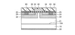
- FIG. 2 is a schematic cross-sectional view showing the structure of a MOSFET in the first embodiment.
- FIG. 3 is a flowchart showing an outline of a manufacturing procedure of a MOSFET in the first embodiment. It is a schematic sectional drawing for demonstrating the manufacturing method of MOSFET. It is a schematic sectional drawing for demonstrating the manufacturing method of MOSFET. It is a schematic sectional drawing for demonstrating the manufacturing method of MOSFET. It is a schematic sectional drawing for demonstrating the manufacturing method of MOSFET. It is a schematic sectional drawing for demonstrating the manufacturing method of MOSFET. It is a schematic sectional drawing for demonstrating the manufacturing method of MOSFET. It is a schematic sectional drawing for demonstrating the manufacturing method of MOSFET. It is a schematic sectional drawing for demonstrating the manufacturing method of MOSFET. It is a schematic sectional drawing for demonstrating the manufacturing method of MOSFET. FIG.
- FIG. 6 is a schematic cross-sectional view showing a structure of a MOSFET in a second embodiment.
- 10 is a flowchart showing an outline of a manufacturing procedure of a MOSFET in the second embodiment. It is a schematic sectional drawing for demonstrating the manufacturing method of MOSFET. It is a schematic sectional drawing for demonstrating the manufacturing method of MOSFET.
- Embodiment 1 which is one embodiment of the present invention will be described with reference to FIG.
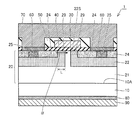
- MOSFET 1 which is a semiconductor device in the first embodiment includes silicon carbide substrate 10 and active layer 20 which is disposed on one main surface 10A of silicon carbide substrate 10 and is an epitaxially grown layer made of silicon carbide.
- Silicon carbide substrate 10 is made of single crystal silicon carbide, and has an n-type conductivity (first conductivity type) by including impurities (n-type impurities) such as nitrogen and phosphorus.
- the active layer 20 includes a drift layer 21, a p-type body region 22, an n + source region 24, and a p + contact region 25.
- Drift layer 21 is arranged on silicon carbide substrate 10 and has an n-type conductivity by containing an n-type impurity at a concentration lower than that of silicon carbide substrate 10.
- P type body region 22 is arranged to include a main surface of active layer 20 opposite to silicon carbide substrate 10.
- the p-type body region 22 includes an impurity (p-type impurity) such as aluminum or boron, so that the conductivity type is p-type (second conductivity type).
- N + source region 24 is formed in p type body region 22 so as to include a main surface of active layer 20 opposite to silicon carbide substrate 10.
- the n + source region 24 includes an n-type impurity at a concentration higher than that of the drift layer 21, so that the conductivity type is n-type.
- P + contact region 25 is formed in p type body region 22 so as to include the main surface of active layer 20 opposite to silicon carbide substrate 10, and viewed from n + source region 24. It is arranged on the center side.
- the p + contact region 25 has a p-type conductivity by including a p-type impurity.
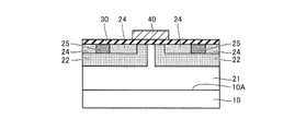
- MOSFET 1 further includes a gate oxide film 30 as a gate insulating film, a gate electrode 40, a source contact electrode 60, an interlayer insulating film 50, a source wiring 70, a drain contact electrode 80, and a back surface protective electrode 90. ing.
- Gate oxide film 30 is made of an insulator such as silicon dioxide and extends so as to be in contact with n + source region 24 and p type body region 22 on the main surface of active layer 20 opposite to silicon carbide substrate 10. Exist. Gate electrode 40 is disposed on and in contact with gate oxide film 30 and extends on p-type body region 22.
- the gate electrode 40 is made of a conductor such as polysilicon or aluminum.
- the source contact electrode 60 is disposed on the active layer 20 so as to be in contact with the n + source region 24 and the p + contact region 25.
- the source contact electrode 60 is disposed so as to contact a region on the active layer 20 that is not covered with the gate oxide film 30.
- the source contact electrode 60 is made of a conductor such as nickel, and at least a region in contact with the active layer 20 is silicided to form an ohmic contact with the n + source region 24.
- the interlayer insulating film 50 is disposed so as to cover the gate electrode 40 and extend to the gate oxide film 30.
- the interlayer insulating film 50 is made of an insulator such as silicon dioxide.
- the source wiring 70 is disposed so as to contact the source contact electrode 60 and cover the source contact electrode 60 and the interlayer insulating film 50.
- the source wiring 70 is made of a conductor such as aluminum.
- the drain contact electrode 80 is arranged in contact with the main surface of the silicon carbide substrate 10 opposite to the active layer 20.
- Drain contact electrode 80 is made of a conductor such as nickel, and at least a region in contact with silicon carbide substrate 10 is silicided to form ohmic contact with silicon carbide substrate 10.
- the back surface protective electrode 90 is disposed so as to contact the drain contact electrode 80 and cover the drain contact electrode 80.
- the back surface protective electrode 90 is made of a conductor such as aluminum.
- MOSFET 1 in the state where the voltage of gate electrode 40 is lower than the threshold voltage, that is, in the off state, p-type body region 22 and drift layer 21 are applied even when a voltage is applied to drain contact electrode 80 and back surface protective electrode 90.
- a voltage equal to or higher than the threshold voltage is applied to the gate electrode 40, an inversion layer is formed in the channel region 29, which is a region near the gate oxide film 30 in the p-type body region 22.
- the n + source region 24 and the drift layer 21 are electrically connected, electrons serving as carriers move along the arrow ⁇ , and a current flows.
- MOSFET 1 which is a semiconductor device in the present embodiment is in contact with silicon carbide substrate 10, active layer 20 made of silicon carbide, which is an epitaxially grown layer formed on silicon carbide substrate 10, and active layer 20.
- a gate oxide film 30 disposed and a gate electrode 40 disposed in contact with the gate oxide film 30 are provided.
- the active layer 20 has a p-type conductivity type, and has a p-type body region 22 in which an inversion layer is formed in a channel region 29 that is in contact with the gate oxide film 30 when a voltage is applied to the gate electrode 40. Including.
- the electron mobility ⁇ in the inversion layer is stronger than the state where the inversion layer is proportional to the reciprocal of the acceptor concentration N a in the channel region 29 is a region to be formed of p-type body region 22 acceptor It depends on the concentration N a.
- the acceptor concentration N a in the channel region 29 of the p-type body region 22 is 1 ⁇ 10 16 cm ⁇ 3 or more and 2 ⁇ 10 18 cm ⁇ 3 or less.
- silicon carbide substrate 10 includes a main surface 10A on the side where active layer 20 that is an epitaxial growth layer is formed, and a (0001) surface of silicon carbide constituting silicon carbide substrate 10.
- the formed angle is 8 ° or less. Therefore, the angle formed by the surface 22S of the active layer 20 facing the gate electrode 40 across the gate oxide film 30 and the (0001) plane of silicon carbide constituting the active layer 20 is 8 ° or less.
- the electron mobility ⁇ in the inversion layer as described above, as compared with the state in proportion to the reciprocal of the acceptor concentration N a in the channel region 29 is a region where an inversion layer is formed of p-type body region 22 It is dependent on the acceptor concentration N a.
- the acceptor concentration N a in the channel region 29 to the inversion layer is formed is not more than 1 ⁇ 10 16 cm -3 or more 2 ⁇ 10 18 cm -3, and the channel length L Is not less than d defined by the expression (3) and not more than 0.43 ⁇ m, the occurrence of the short channel effect is suppressed and the channel resistance is reduced.
- MOSFET 1 is a semiconductor device with reduced channel resistance.
- MOSFET 1 for example, 1.7 ⁇ 10 ⁇ 18 as the value of B and 0.98 as the value of C can be adopted.
- the optimum acceptor density N a case can be calculated is 5.8 ⁇ 10 17 cm -3 on the basis of the equation (4).
- the minimum channel length L that can suppress the short channel effect is 0.01 ⁇ m.
- the acceptor density N a and channel length L for example, the acceptor density N a is 1 ⁇ 10 16 cm ⁇ 3 and the channel length L is 0.5 ⁇ m, which is 1/30. Channel resistance can be reduced.
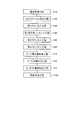
- a substrate preparation step is first performed as a step (S10).
- step (S10) referring to FIG. 3, for example, it is collected from an ingot of single crystal silicon carbide produced by, for example, a sublimation method, and has main surface 10A whose angle with (0001) plane is 8 ° or less. Silicon carbide substrate 10 is prepared.
- drift layer 21 having an n conductivity type is formed on one main surface 10A of silicon carbide substrate 10 by epitaxial growth.
- nitrogen, phosphorus, or the like can be employed as an n-type impurity for making the conductivity type n-type.
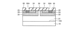
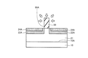
- a first ion implantation step is performed as a step (S30).
- step (S30) referring to FIG. 4, first, mask layer 99 having opening 99A is formed on drift layer 21.
- Mask layer 99 may be made of, for example, silicon dioxide.
- ion implantation is performed using mask layer 99 as a mask, thereby forming n + region 24A containing an n-type impurity having a concentration higher than that of drift layer 21.
- a first isotropic etching step is performed as a step (S40).
- this step (S40) referring to FIG. 5, by performing isotropic etching on mask layer 99 used in step (S30), opening 99A is enlarged as shown by an arrow.
- a second ion implantation step is performed as a step (S50).
- ion implantation is performed using mask layer 99 in which opening 99A is enlarged in step (S40) as a mask, thereby forming p-type body region 22 containing a p-type impurity.
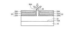
- a third ion implantation step is performed.
- this step (S60) referring to FIG. 6, after mask layer 99 used in step (S50) is once removed, mask layer 99 having opening 99A at an appropriate position is formed again. Thereafter, by performing ion implantation using the mask layer 99 as a mask, the p + contact region 25 containing a high concentration p-type impurity is formed. At this time, a region in which the p + contact region 25 is not formed in the n + region 24A becomes the n + source region 24.
- a gate oxide film forming step is performed as a step (S70).
- step (S70) referring to FIG. 6 and FIG. 7, the mask layer 99 used in step (S60) is removed, and then the thermal oxidation process is performed, whereby gate oxide film 30 and A thermal oxide film 30 to be formed is formed.
- Thermal oxide film 30 is formed so as to cover the entire main surface of drift layer 21 opposite to silicon carbide substrate 10.
- a gate electrode formation step is performed as a step (S80).
- step (S80) referring to FIGS. 7 and 8, gate electrode 40 made of, for example, polysilicon is formed so as to be in contact with thermal oxide film 30.
- the formation of the gate electrode 40 can be performed by sputtering, for example.
- a contact electrode forming step is performed as a step (S90).
- step (S90) referring to FIGS. 8 and 9, source contact electrode 60 and drain contact electrode 80 are formed. Specifically, first, the thermal oxide film 30 on the region to be in contact with the source contact electrode 60 in the n + source region 24 and the p + contact region 25 is removed by etching. Next, for example, a nickel film is formed by vapor deposition in a desired region where the source contact electrode 60 and the drain contact electrode 80 are to be formed. Further, an interlayer insulating film 50 made of silicon dioxide is formed so as to cover the upper surfaces of the nickel film and the thermal oxide film 30 to be the gate electrode 40 and the source contact electrode 60.
- source contact electrode 60 that forms an ohmic contact with n + source region 24
- drain contact electrode 80 that forms an ohmic contact with silicon carbide substrate 10, and interlayer insulating film 50 are formed.
- a wiring formation step is performed as a step (S100).
- step (S100) referring to FIG. 9 and FIG. 1, source wiring 70 and back surface protection electrode 90 are formed. Specifically, for example, after the interlayer insulating film 50 on the source contact electrode 60 is removed, aluminum is deposited so as to cover the source contact electrode 60 and the interlayer insulating film 50 and the drain contact electrode 80.
- the manufacturing process of MOSFET 1 in the present embodiment is completed.
- the channel length L is determined by isotropic etching in the step (S40). By setting the channel length L to 0.1 ⁇ m or more, the value of the channel length L can be controlled relatively easily.
- MOSFET 1 which is a semiconductor device in the second embodiment has basically the same structure as MOSFET 1 in the first embodiment and has the same effects.
- MOSFET 1 in the second embodiment is different from that in the first embodiment in the configuration of p-type body region 22, particularly in the configuration of channel region 29.
- p-type body region 22 is arranged so as to surround high concentration region 22A including a high concentration acceptor and high concentration region 22A, and high concentration region 22A. And a low concentration region 22B including an acceptor having a lower concentration.
- the gate oxide film 30 extends so as to be in contact with the n + source region 24, the high concentration region 22A, and the low concentration region 22B.
- the gate electrode 40 extends from the high concentration region 22A to the low concentration region 22B.
- p-type body region 22 is arranged to include a channel region 29 where an inversion layer is to be formed, and high-concentration region 22A having a high acceptor concentration and electrons in the inversion layer are arranged. It has a low concentration region 22B that is adjacent to the high concentration region 22A in the movement direction ⁇ and includes the channel region 29 and has a lower acceptor concentration than the high concentration region 22A.
- high concentration region 22A suppresses the spread width of the depletion layer in channel region 29 where the inversion layer is to be formed, and more reliably suppresses the occurrence of the short channel effect. Can do.
- the acceptor concentration in low concentration region 22B is 1 ⁇ 2 or less of the acceptor concentration in high concentration region 22A.
- the substrate preparation step as step (S110), the epitaxial growth step as step (S120), and the first ion implantation step as step (S130) are performed.
- Each is carried out in the same manner as steps (S10), (S20) and (S30) in the first embodiment.
- a first isotropic etching step is performed as a step (S140).
- this step (S140) referring to FIG. 12, by performing isotropic etching on mask layer 99 used in step (S130), an opening corresponding to the shape of desired high concentration region 22A.
- the opening 99A is enlarged as indicated by the arrow so that 99A is formed.
- a second ion implantation step is performed as a step (S150).
- ion implantation is performed using the mask layer 99 in which the opening 99A is enlarged in the step (S140) as a mask, thereby forming a high concentration region 22A including a high concentration acceptor.
- a high-concentration p-type impurity is introduced by ion implantation in the step (S150), and a predetermined ratio of impurities introduced by subsequent activation annealing functions as an acceptor.
- a density region 22A is formed.
- a second isotropic etching step is performed as a step (S151).
- this step (S151) referring to FIG. 13, by performing isotropic etching on mask layer 99 used in step (S150), an opening corresponding to the shape of desired low-concentration region 22B.
- the opening 99A is enlarged as indicated by the arrow so that 99A is formed.
- a fourth ion implantation step is performed as a step (S152).
- ion implantation is performed using the mask layer 99 in which the opening 99A is enlarged in the step (S151) as a mask, thereby forming a low concentration region 22B having an acceptor concentration lower than that of the high concentration region 22A.
- a p-type impurity having a concentration lower than that of the high-concentration region 22A is introduced by ion implantation, and a predetermined proportion of the impurities introduced by the subsequent activation annealing serves as an acceptor. By functioning, the low concentration region 22B is formed.
- a third ion implantation step as a step (S160), a gate oxide film formation step as a step (S170), a gate electrode formation step as a step (S180), a contact electrode formation step as a step (S190), and (S200) ) Is performed in the same manner as steps (S60), (S70), (S80), (S90), and (S100) of the first embodiment.
- the semiconductor device of the present invention is applied to a DMOSFET (planar type MOSFET) has been described.
- the semiconductor device of the present invention is not limited to this, and a channel is formed with a predetermined threshold voltage as a boundary.
- the present invention can be applied to various semiconductor devices that control whether or not an inversion layer is formed in a region to conduct and block current.
- the semiconductor device of the present invention can be widely applied to semiconductor devices such as trench MOSFET (UMOSFET), VMOSFET, and IGBT, for example.
- the semiconductor device of the present invention can be particularly advantageously applied to a semiconductor device that is required to reduce on-resistance.
- MOSFET 10 silicon carbide substrate, 10A main surface, 20 active layer, 21 drift layer, 22 p-type body region, 22A high concentration region, 22B low concentration region, 22S surface, 24 n + source region, 24A n + region, 25 p + contact region, 29 channel region, 30 gate oxide film (thermal oxide film), 40 gate electrode, 50 interlayer insulating film, 60 source contact electrode, 70 source wiring, 80 drain contact electrode, 90 back surface protection electrode, 99 mask Layer, 99A opening.
Landscapes
- Electrodes Of Semiconductors (AREA)
- Insulated Gate Type Field-Effect Transistor (AREA)
Priority Applications (3)
| Application Number | Priority Date | Filing Date | Title |
|---|---|---|---|
| EP11857887.1A EP2672516A4 (en) | 2011-02-01 | 2011-10-05 | SEMICONDUCTOR COMPONENT |
| KR1020137015257A KR20140001947A (ko) | 2011-02-01 | 2011-10-05 | 반도체 장치 |
| CN201180063838.XA CN103843141A (zh) | 2011-02-01 | 2011-10-05 | 半导体器件 |
Applications Claiming Priority (2)
| Application Number | Priority Date | Filing Date | Title |
|---|---|---|---|
| JP2011-019372 | 2011-02-01 | ||
| JP2011019372A JP2012160584A (ja) | 2011-02-01 | 2011-02-01 | 半導体装置 |
Publications (1)
| Publication Number | Publication Date |
|---|---|
| WO2012105088A1 true WO2012105088A1 (ja) | 2012-08-09 |
Family
ID=46576607
Family Applications (1)
| Application Number | Title | Priority Date | Filing Date |
|---|---|---|---|
| PCT/JP2011/072992 WO2012105088A1 (ja) | 2011-02-01 | 2011-10-05 | 半導体装置 |
Country Status (7)
Families Citing this family (17)
| Publication number | Priority date | Publication date | Assignee | Title |
|---|---|---|---|---|
| EP2682593A3 (en) * | 2012-07-03 | 2018-09-12 | Fuji Electric Co., Ltd. | Ignition device with single chip for internal combustion engine |
| US9240476B2 (en) * | 2013-03-13 | 2016-01-19 | Cree, Inc. | Field effect transistor devices with buried well regions and epitaxial layers |
| US9306061B2 (en) | 2013-03-13 | 2016-04-05 | Cree, Inc. | Field effect transistor devices with protective regions |
| US9142668B2 (en) | 2013-03-13 | 2015-09-22 | Cree, Inc. | Field effect transistor devices with buried well protection regions |
| US9012984B2 (en) | 2013-03-13 | 2015-04-21 | Cree, Inc. | Field effect transistor devices with regrown p-layers |
| JP2015053462A (ja) * | 2013-08-06 | 2015-03-19 | 住友電気工業株式会社 | 炭化珪素半導体装置およびその製造方法 |
| JP6256148B2 (ja) * | 2014-03-27 | 2018-01-10 | 住友電気工業株式会社 | 炭化珪素半導体装置およびその製造方法 |
| JP2016029707A (ja) * | 2014-07-24 | 2016-03-03 | 住友電気工業株式会社 | 炭化珪素半導体装置 |
| JP6481511B2 (ja) * | 2014-07-24 | 2019-03-13 | 住友電気工業株式会社 | 炭化珪素半導体装置 |
| DE102016226237B4 (de) * | 2016-02-01 | 2024-07-18 | Fuji Electric Co., Ltd. | Siliziumcarbid-halbleitervorrichtung |
| JP6115678B1 (ja) | 2016-02-01 | 2017-04-19 | 富士電機株式会社 | 炭化珪素半導体装置および炭化珪素半導体装置の製造方法 |
| DE112017005529B4 (de) * | 2016-11-01 | 2024-03-14 | Mitsubishi Electric Corporation | Siliciumcarbid-halbleitereinheit und leistungswandlereinheit |
| JP7155634B2 (ja) * | 2018-06-12 | 2022-10-19 | 富士電機株式会社 | 炭化珪素半導体装置および炭化珪素半導体装置の製造方法 |
| US10957791B2 (en) * | 2019-03-08 | 2021-03-23 | Infineon Technologies Americas Corp. | Power device with low gate charge and low figure of merit |
| US11658214B2 (en) | 2021-01-12 | 2023-05-23 | Semiconductor Components Industries, Llc | MOSFET device with undulating channel |
| IT202100001895A1 (it) | 2021-01-29 | 2022-07-29 | St Microelectronics Srl | Dispositivo mosfet a conduzione verticale in carburo di silicio per applicazioni di potenza e relativo processo di fabbricazione |
| IT202100001934A1 (it) * | 2021-01-29 | 2022-07-29 | St Microelectronics Srl | Dispositivo mosfet a conduzione verticale in carburo di silicio e relativo processo di fabbricazione |
Citations (5)
| Publication number | Priority date | Publication date | Assignee | Title |
|---|---|---|---|---|
| JP2000150866A (ja) | 1998-09-01 | 2000-05-30 | Fuji Electric Co Ltd | 炭化けい素nチャネルMOS半導体素子およびその製造方法 |
| JP2005252157A (ja) * | 2004-03-08 | 2005-09-15 | Mitsubishi Electric Corp | 半導体装置及びその製造方法 |
| WO2007046254A1 (ja) * | 2005-10-19 | 2007-04-26 | Mitsubishi Electric Corporation | Mosfetおよびmosfetの製造方法 |
| JP2009054765A (ja) * | 2007-08-27 | 2009-03-12 | Mitsubishi Electric Corp | 炭化珪素半導体装置およびその製造方法 |
| JP2010135789A (ja) * | 2008-12-01 | 2010-06-17 | Cree Inc | 低角度オフカット炭化ケイ素結晶上の安定なパワーデバイス |
Family Cites Families (11)
| Publication number | Priority date | Publication date | Assignee | Title |
|---|---|---|---|---|
| JP4371521B2 (ja) * | 2000-03-06 | 2009-11-25 | 株式会社東芝 | 電力用半導体素子およびその製造方法 |
| US7217950B2 (en) * | 2002-10-11 | 2007-05-15 | Nissan Motor Co., Ltd. | Insulated gate tunnel-injection device having heterojunction and method for manufacturing the same |
| US7364978B2 (en) * | 2003-04-25 | 2008-04-29 | Sumitomo Electric Industries, Ltd. | Method of fabricating semiconductor device |
| DE112006002377B4 (de) * | 2005-09-08 | 2014-04-24 | Mitsubishi Denki K.K. | Halbleitervorrichtung und Verfahren zum Herstellen einer Halbleitervorrichtung |
| JP4627272B2 (ja) * | 2006-03-09 | 2011-02-09 | 三菱電機株式会社 | 炭化珪素半導体装置および炭化珪素半導体装置の製造方法 |
| EP2293336B1 (en) * | 2008-05-20 | 2019-11-27 | Rohm Co., Ltd. | Semiconductor device |
| JP5564890B2 (ja) * | 2008-12-16 | 2014-08-06 | 住友電気工業株式会社 | 接合型電界効果トランジスタおよびその製造方法 |
| IT1392577B1 (it) * | 2008-12-30 | 2012-03-09 | St Microelectronics Rousset | Processo di fabbricazione di un dispositivo elettronico di potenza integrato in un substrato semiconduttore ad ampio intervallo di banda proibita e dispositivo elettronico cosi' ottenuto |
| US8653535B2 (en) * | 2010-09-06 | 2014-02-18 | Panasonic Corporation | Silicon carbide semiconductor device having a contact region that includes a first region and a second region, and process for production thereof |
| CA2780359A1 (en) * | 2010-12-22 | 2012-06-22 | Sumitomo Electric Industries, Ltd. | Method of manufacturing silicon carbide semiconductor device |
| JP5777455B2 (ja) * | 2011-09-08 | 2015-09-09 | 株式会社東芝 | 半導体装置および半導体装置の製造方法 |
-
2011
- 2011-02-01 JP JP2011019372A patent/JP2012160584A/ja active Pending
- 2011-10-05 CN CN201180063838.XA patent/CN103843141A/zh active Pending
- 2011-10-05 KR KR1020137015257A patent/KR20140001947A/ko not_active Withdrawn
- 2011-10-05 WO PCT/JP2011/072992 patent/WO2012105088A1/ja active Application Filing
- 2011-10-05 EP EP11857887.1A patent/EP2672516A4/en not_active Withdrawn
- 2011-10-12 TW TW100137035A patent/TW201234592A/zh unknown
-
2012
- 2012-02-01 US US13/364,174 patent/US20120193643A1/en not_active Abandoned
Patent Citations (5)
| Publication number | Priority date | Publication date | Assignee | Title |
|---|---|---|---|---|
| JP2000150866A (ja) | 1998-09-01 | 2000-05-30 | Fuji Electric Co Ltd | 炭化けい素nチャネルMOS半導体素子およびその製造方法 |
| JP2005252157A (ja) * | 2004-03-08 | 2005-09-15 | Mitsubishi Electric Corp | 半導体装置及びその製造方法 |
| WO2007046254A1 (ja) * | 2005-10-19 | 2007-04-26 | Mitsubishi Electric Corporation | Mosfetおよびmosfetの製造方法 |
| JP2009054765A (ja) * | 2007-08-27 | 2009-03-12 | Mitsubishi Electric Corp | 炭化珪素半導体装置およびその製造方法 |
| JP2010135789A (ja) * | 2008-12-01 | 2010-06-17 | Cree Inc | 低角度オフカット炭化ケイ素結晶上の安定なパワーデバイス |
Non-Patent Citations (3)
| Title |
|---|
| FUJIHIRA ET AL.: "Realization of Low On-Resistance 4H-SiC power MOSFETs by Using Retrograde Profile in P-Body", MATERIALS SCIENCE FORUM, vol. 556-557, 2006, pages 827 - 830 |
| See also references of EP2672516A4 |
| SEI-HYUNG RYU ET AL.: "Critical Issues for MOS Based Power Devices in 4H-SiC", MATERIALS SCIENCE FORUM, vol. 615-617, 2009, pages 743 - 748 |
Also Published As
| Publication number | Publication date |
|---|---|
| EP2672516A1 (en) | 2013-12-11 |
| CN103843141A (zh) | 2014-06-04 |
| JP2012160584A (ja) | 2012-08-23 |
| TW201234592A (en) | 2012-08-16 |
| KR20140001947A (ko) | 2014-01-07 |
| US20120193643A1 (en) | 2012-08-02 |
| EP2672516A4 (en) | 2014-08-06 |
Similar Documents
| Publication | Publication Date | Title |
|---|---|---|
| WO2012105088A1 (ja) | 半導体装置 | |
| CN102770960B (zh) | 半导体器件及其制造方法 | |
| US8658503B2 (en) | Semiconductor device and method of fabricating the same | |
| CN106796955B (zh) | 半导体装置 | |
| JP5577478B1 (ja) | 半導体装置 | |
| US10886365B2 (en) | Semiconductor device and method of manufacturing semiconductor device | |
| WO2012132509A1 (ja) | Igbt | |
| JP2011023675A (ja) | 半導体装置及びその製造方法 | |
| WO2013001677A1 (ja) | 半導体装置とその製造方法 | |
| JP2012253293A (ja) | 半導体装置 | |
| JP2012164707A (ja) | 半導体装置およびその製造方法 | |
| EP3479410A1 (en) | Short channel trench power mosfet | |
| US9786741B2 (en) | Silicon carbide semiconductor device and method for manufacturing the same | |
| US20170125575A1 (en) | Silicon carbide semiconductor element and method for manufacturing the same | |
| US20130134442A1 (en) | Semiconductor device and method for manufacturing same | |
| CN108604600A (zh) | 碳化硅半导体装置及其制造方法 | |
| JP6550869B2 (ja) | 半導体装置 | |
| US8766277B2 (en) | Semiconductor device and manufacturing method of the same | |
| JP7150609B2 (ja) | 短チャネルのトレンチパワーmosfet | |
| JP6651801B2 (ja) | 半導体装置および半導体装置の製造方法 | |
| JP6207627B2 (ja) | 半導体装置 | |
| JP5059989B1 (ja) | 半導体装置とその製造方法 | |
| JP6822088B2 (ja) | 炭化珪素半導体装置および炭化珪素半導体装置の製造方法 | |
| JP2024138816A (ja) | 半導体装置及び半導体装置の製造方法 |
Legal Events
| Date | Code | Title | Description |
|---|---|---|---|
| 121 | Ep: the epo has been informed by wipo that ep was designated in this application |
Ref document number: 11857887 Country of ref document: EP Kind code of ref document: A1 |
|
| ENP | Entry into the national phase |
Ref document number: 20137015257 Country of ref document: KR Kind code of ref document: A |
|
| WWE | Wipo information: entry into national phase |
Ref document number: 2011857887 Country of ref document: EP |
|
| NENP | Non-entry into the national phase |
Ref country code: DE |