WO2012102303A1 - 電子部品モジュールおよび電子部品素子 - Google Patents
電子部品モジュールおよび電子部品素子 Download PDFInfo
- Publication number
- WO2012102303A1 WO2012102303A1 PCT/JP2012/051544 JP2012051544W WO2012102303A1 WO 2012102303 A1 WO2012102303 A1 WO 2012102303A1 JP 2012051544 W JP2012051544 W JP 2012051544W WO 2012102303 A1 WO2012102303 A1 WO 2012102303A1
- Authority
- WO
- WIPO (PCT)
- Prior art keywords
- electronic component
- electrode
- substrate
- solder
- component module
- Prior art date
Links
- 229910000679 solder Inorganic materials 0.000 claims abstract description 79
- 239000000758 substrate Substances 0.000 claims abstract description 75
- 239000011347 resin Substances 0.000 claims description 11
- 229920005989 resin Polymers 0.000 claims description 11
- 238000000034 method Methods 0.000 description 9
- 239000000463 material Substances 0.000 description 8
- 238000004519 manufacturing process Methods 0.000 description 6
- 239000004065 semiconductor Substances 0.000 description 6
- 229910052751 metal Inorganic materials 0.000 description 5
- 239000002184 metal Substances 0.000 description 5
- 239000004020 conductor Substances 0.000 description 4
- 238000000206 photolithography Methods 0.000 description 3
- 238000007747 plating Methods 0.000 description 3
- 239000003990 capacitor Substances 0.000 description 2
- 229910052802 copper Inorganic materials 0.000 description 2
- 238000010438 heat treatment Methods 0.000 description 2
- 230000001678 irradiating effect Effects 0.000 description 2
- 150000002739 metals Chemical class 0.000 description 2
- 229910052759 nickel Inorganic materials 0.000 description 2
- 229910052763 palladium Inorganic materials 0.000 description 2
- 229910052697 platinum Inorganic materials 0.000 description 2
- 230000001846 repelling effect Effects 0.000 description 2
- 238000007740 vapor deposition Methods 0.000 description 2
- 229910004298 SiO 2 Inorganic materials 0.000 description 1
- 230000015572 biosynthetic process Effects 0.000 description 1
- 239000000919 ceramic Substances 0.000 description 1
- 230000000694 effects Effects 0.000 description 1
- 238000005530 etching Methods 0.000 description 1
- 238000005304 joining Methods 0.000 description 1
- 238000012986 modification Methods 0.000 description 1
- 230000004048 modification Effects 0.000 description 1
- 229910052709 silver Inorganic materials 0.000 description 1
- 238000005476 soldering Methods 0.000 description 1
- 238000004544 sputter deposition Methods 0.000 description 1
Images


Classifications
-
- H—ELECTRICITY
- H01—ELECTRIC ELEMENTS
- H01L—SEMICONDUCTOR DEVICES NOT COVERED BY CLASS H10
- H01L23/00—Details of semiconductor or other solid state devices
- H01L23/28—Encapsulations, e.g. encapsulating layers, coatings, e.g. for protection
- H01L23/31—Encapsulations, e.g. encapsulating layers, coatings, e.g. for protection characterised by the arrangement or shape
- H01L23/3107—Encapsulations, e.g. encapsulating layers, coatings, e.g. for protection characterised by the arrangement or shape the device being completely enclosed
- H01L23/315—Encapsulations, e.g. encapsulating layers, coatings, e.g. for protection characterised by the arrangement or shape the device being completely enclosed the encapsulation having a cavity
-
- H—ELECTRICITY
- H01—ELECTRIC ELEMENTS
- H01L—SEMICONDUCTOR DEVICES NOT COVERED BY CLASS H10
- H01L24/00—Arrangements for connecting or disconnecting semiconductor or solid-state bodies; Methods or apparatus related thereto
- H01L24/01—Means for bonding being attached to, or being formed on, the surface to be connected, e.g. chip-to-package, die-attach, "first-level" interconnects; Manufacturing methods related thereto
- H01L24/10—Bump connectors ; Manufacturing methods related thereto
- H01L24/11—Manufacturing methods
-
- H—ELECTRICITY
- H01—ELECTRIC ELEMENTS
- H01L—SEMICONDUCTOR DEVICES NOT COVERED BY CLASS H10
- H01L24/00—Arrangements for connecting or disconnecting semiconductor or solid-state bodies; Methods or apparatus related thereto
- H01L24/01—Means for bonding being attached to, or being formed on, the surface to be connected, e.g. chip-to-package, die-attach, "first-level" interconnects; Manufacturing methods related thereto
- H01L24/10—Bump connectors ; Manufacturing methods related thereto
- H01L24/12—Structure, shape, material or disposition of the bump connectors prior to the connecting process
- H01L24/13—Structure, shape, material or disposition of the bump connectors prior to the connecting process of an individual bump connector
-
- H—ELECTRICITY
- H01—ELECTRIC ELEMENTS
- H01L—SEMICONDUCTOR DEVICES NOT COVERED BY CLASS H10
- H01L21/00—Processes or apparatus adapted for the manufacture or treatment of semiconductor or solid state devices or of parts thereof
- H01L21/02—Manufacture or treatment of semiconductor devices or of parts thereof
- H01L21/04—Manufacture or treatment of semiconductor devices or of parts thereof the devices having potential barriers, e.g. a PN junction, depletion layer or carrier concentration layer
- H01L21/50—Assembly of semiconductor devices using processes or apparatus not provided for in a single one of the subgroups H01L21/06 - H01L21/326, e.g. sealing of a cap to a base of a container
- H01L21/56—Encapsulations, e.g. encapsulation layers, coatings
- H01L21/563—Encapsulation of active face of flip-chip device, e.g. underfilling or underencapsulation of flip-chip, encapsulation preform on chip or mounting substrate
-
- H—ELECTRICITY
- H01—ELECTRIC ELEMENTS
- H01L—SEMICONDUCTOR DEVICES NOT COVERED BY CLASS H10
- H01L2224/00—Indexing scheme for arrangements for connecting or disconnecting semiconductor or solid-state bodies and methods related thereto as covered by H01L24/00
- H01L2224/01—Means for bonding being attached to, or being formed on, the surface to be connected, e.g. chip-to-package, die-attach, "first-level" interconnects; Manufacturing methods related thereto
- H01L2224/02—Bonding areas; Manufacturing methods related thereto
- H01L2224/04—Structure, shape, material or disposition of the bonding areas prior to the connecting process
- H01L2224/0401—Bonding areas specifically adapted for bump connectors, e.g. under bump metallisation [UBM]
-
- H—ELECTRICITY
- H01—ELECTRIC ELEMENTS
- H01L—SEMICONDUCTOR DEVICES NOT COVERED BY CLASS H10
- H01L2224/00—Indexing scheme for arrangements for connecting or disconnecting semiconductor or solid-state bodies and methods related thereto as covered by H01L24/00
- H01L2224/01—Means for bonding being attached to, or being formed on, the surface to be connected, e.g. chip-to-package, die-attach, "first-level" interconnects; Manufacturing methods related thereto
- H01L2224/02—Bonding areas; Manufacturing methods related thereto
- H01L2224/04—Structure, shape, material or disposition of the bonding areas prior to the connecting process
- H01L2224/05—Structure, shape, material or disposition of the bonding areas prior to the connecting process of an individual bonding area
- H01L2224/0554—External layer
- H01L2224/0556—Disposition
- H01L2224/05567—Disposition the external layer being at least partially embedded in the surface
-
- H—ELECTRICITY
- H01—ELECTRIC ELEMENTS
- H01L—SEMICONDUCTOR DEVICES NOT COVERED BY CLASS H10
- H01L2224/00—Indexing scheme for arrangements for connecting or disconnecting semiconductor or solid-state bodies and methods related thereto as covered by H01L24/00
- H01L2224/01—Means for bonding being attached to, or being formed on, the surface to be connected, e.g. chip-to-package, die-attach, "first-level" interconnects; Manufacturing methods related thereto
- H01L2224/02—Bonding areas; Manufacturing methods related thereto
- H01L2224/04—Structure, shape, material or disposition of the bonding areas prior to the connecting process
- H01L2224/05—Structure, shape, material or disposition of the bonding areas prior to the connecting process of an individual bonding area
- H01L2224/0554—External layer
- H01L2224/05599—Material
- H01L2224/056—Material with a principal constituent of the material being a metal or a metalloid, e.g. boron [B], silicon [Si], germanium [Ge], arsenic [As], antimony [Sb], tellurium [Te] and polonium [Po], and alloys thereof
- H01L2224/05617—Material with a principal constituent of the material being a metal or a metalloid, e.g. boron [B], silicon [Si], germanium [Ge], arsenic [As], antimony [Sb], tellurium [Te] and polonium [Po], and alloys thereof the principal constituent melting at a temperature of greater than or equal to 400°C and less than 950°C
- H01L2224/05624—Aluminium [Al] as principal constituent
-
- H—ELECTRICITY
- H01—ELECTRIC ELEMENTS
- H01L—SEMICONDUCTOR DEVICES NOT COVERED BY CLASS H10
- H01L2224/00—Indexing scheme for arrangements for connecting or disconnecting semiconductor or solid-state bodies and methods related thereto as covered by H01L24/00
- H01L2224/01—Means for bonding being attached to, or being formed on, the surface to be connected, e.g. chip-to-package, die-attach, "first-level" interconnects; Manufacturing methods related thereto
- H01L2224/10—Bump connectors; Manufacturing methods related thereto
- H01L2224/1012—Auxiliary members for bump connectors, e.g. spacers
- H01L2224/10122—Auxiliary members for bump connectors, e.g. spacers being formed on the semiconductor or solid-state body to be connected
- H01L2224/10135—Alignment aids
-
- H—ELECTRICITY
- H01—ELECTRIC ELEMENTS
- H01L—SEMICONDUCTOR DEVICES NOT COVERED BY CLASS H10
- H01L2224/00—Indexing scheme for arrangements for connecting or disconnecting semiconductor or solid-state bodies and methods related thereto as covered by H01L24/00
- H01L2224/01—Means for bonding being attached to, or being formed on, the surface to be connected, e.g. chip-to-package, die-attach, "first-level" interconnects; Manufacturing methods related thereto
- H01L2224/10—Bump connectors; Manufacturing methods related thereto
- H01L2224/1012—Auxiliary members for bump connectors, e.g. spacers
- H01L2224/10122—Auxiliary members for bump connectors, e.g. spacers being formed on the semiconductor or solid-state body to be connected
- H01L2224/10145—Flow barriers
-
- H—ELECTRICITY
- H01—ELECTRIC ELEMENTS
- H01L—SEMICONDUCTOR DEVICES NOT COVERED BY CLASS H10
- H01L2224/00—Indexing scheme for arrangements for connecting or disconnecting semiconductor or solid-state bodies and methods related thereto as covered by H01L24/00
- H01L2224/01—Means for bonding being attached to, or being formed on, the surface to be connected, e.g. chip-to-package, die-attach, "first-level" interconnects; Manufacturing methods related thereto
- H01L2224/10—Bump connectors; Manufacturing methods related thereto
- H01L2224/11—Manufacturing methods
- H01L2224/114—Manufacturing methods by blanket deposition of the material of the bump connector
- H01L2224/1146—Plating
-
- H—ELECTRICITY
- H01—ELECTRIC ELEMENTS
- H01L—SEMICONDUCTOR DEVICES NOT COVERED BY CLASS H10
- H01L2224/00—Indexing scheme for arrangements for connecting or disconnecting semiconductor or solid-state bodies and methods related thereto as covered by H01L24/00
- H01L2224/01—Means for bonding being attached to, or being formed on, the surface to be connected, e.g. chip-to-package, die-attach, "first-level" interconnects; Manufacturing methods related thereto
- H01L2224/10—Bump connectors; Manufacturing methods related thereto
- H01L2224/11—Manufacturing methods
- H01L2224/1147—Manufacturing methods using a lift-off mask
-
- H—ELECTRICITY
- H01—ELECTRIC ELEMENTS
- H01L—SEMICONDUCTOR DEVICES NOT COVERED BY CLASS H10
- H01L2224/00—Indexing scheme for arrangements for connecting or disconnecting semiconductor or solid-state bodies and methods related thereto as covered by H01L24/00
- H01L2224/01—Means for bonding being attached to, or being formed on, the surface to be connected, e.g. chip-to-package, die-attach, "first-level" interconnects; Manufacturing methods related thereto
- H01L2224/10—Bump connectors; Manufacturing methods related thereto
- H01L2224/11—Manufacturing methods
- H01L2224/118—Post-treatment of the bump connector
- H01L2224/11848—Thermal treatments, e.g. annealing, controlled cooling
- H01L2224/11849—Reflowing
-
- H—ELECTRICITY
- H01—ELECTRIC ELEMENTS
- H01L—SEMICONDUCTOR DEVICES NOT COVERED BY CLASS H10
- H01L2224/00—Indexing scheme for arrangements for connecting or disconnecting semiconductor or solid-state bodies and methods related thereto as covered by H01L24/00
- H01L2224/01—Means for bonding being attached to, or being formed on, the surface to be connected, e.g. chip-to-package, die-attach, "first-level" interconnects; Manufacturing methods related thereto
- H01L2224/10—Bump connectors; Manufacturing methods related thereto
- H01L2224/12—Structure, shape, material or disposition of the bump connectors prior to the connecting process
- H01L2224/13—Structure, shape, material or disposition of the bump connectors prior to the connecting process of an individual bump connector
- H01L2224/13001—Core members of the bump connector
- H01L2224/1302—Disposition
- H01L2224/13021—Disposition the bump connector being disposed in a recess of the surface
-
- H—ELECTRICITY
- H01—ELECTRIC ELEMENTS
- H01L—SEMICONDUCTOR DEVICES NOT COVERED BY CLASS H10
- H01L2224/00—Indexing scheme for arrangements for connecting or disconnecting semiconductor or solid-state bodies and methods related thereto as covered by H01L24/00
- H01L2224/01—Means for bonding being attached to, or being formed on, the surface to be connected, e.g. chip-to-package, die-attach, "first-level" interconnects; Manufacturing methods related thereto
- H01L2224/10—Bump connectors; Manufacturing methods related thereto
- H01L2224/12—Structure, shape, material or disposition of the bump connectors prior to the connecting process
- H01L2224/13—Structure, shape, material or disposition of the bump connectors prior to the connecting process of an individual bump connector
- H01L2224/13001—Core members of the bump connector
- H01L2224/13075—Plural core members
- H01L2224/1308—Plural core members being stacked
- H01L2224/13082—Two-layer arrangements
-
- H—ELECTRICITY
- H01—ELECTRIC ELEMENTS
- H01L—SEMICONDUCTOR DEVICES NOT COVERED BY CLASS H10
- H01L2224/00—Indexing scheme for arrangements for connecting or disconnecting semiconductor or solid-state bodies and methods related thereto as covered by H01L24/00
- H01L2224/01—Means for bonding being attached to, or being formed on, the surface to be connected, e.g. chip-to-package, die-attach, "first-level" interconnects; Manufacturing methods related thereto
- H01L2224/10—Bump connectors; Manufacturing methods related thereto
- H01L2224/12—Structure, shape, material or disposition of the bump connectors prior to the connecting process
- H01L2224/13—Structure, shape, material or disposition of the bump connectors prior to the connecting process of an individual bump connector
- H01L2224/13001—Core members of the bump connector
- H01L2224/13099—Material
- H01L2224/131—Material with a principal constituent of the material being a metal or a metalloid, e.g. boron [B], silicon [Si], germanium [Ge], arsenic [As], antimony [Sb], tellurium [Te] and polonium [Po], and alloys thereof
- H01L2224/13138—Material with a principal constituent of the material being a metal or a metalloid, e.g. boron [B], silicon [Si], germanium [Ge], arsenic [As], antimony [Sb], tellurium [Te] and polonium [Po], and alloys thereof the principal constituent melting at a temperature of greater than or equal to 950°C and less than 1550°C
- H01L2224/13147—Copper [Cu] as principal constituent
-
- H—ELECTRICITY
- H01—ELECTRIC ELEMENTS
- H01L—SEMICONDUCTOR DEVICES NOT COVERED BY CLASS H10
- H01L2224/00—Indexing scheme for arrangements for connecting or disconnecting semiconductor or solid-state bodies and methods related thereto as covered by H01L24/00
- H01L2224/01—Means for bonding being attached to, or being formed on, the surface to be connected, e.g. chip-to-package, die-attach, "first-level" interconnects; Manufacturing methods related thereto
- H01L2224/10—Bump connectors; Manufacturing methods related thereto
- H01L2224/12—Structure, shape, material or disposition of the bump connectors prior to the connecting process
- H01L2224/13—Structure, shape, material or disposition of the bump connectors prior to the connecting process of an individual bump connector
- H01L2224/13001—Core members of the bump connector
- H01L2224/13099—Material
- H01L2224/131—Material with a principal constituent of the material being a metal or a metalloid, e.g. boron [B], silicon [Si], germanium [Ge], arsenic [As], antimony [Sb], tellurium [Te] and polonium [Po], and alloys thereof
- H01L2224/13138—Material with a principal constituent of the material being a metal or a metalloid, e.g. boron [B], silicon [Si], germanium [Ge], arsenic [As], antimony [Sb], tellurium [Te] and polonium [Po], and alloys thereof the principal constituent melting at a temperature of greater than or equal to 950°C and less than 1550°C
- H01L2224/13155—Nickel [Ni] as principal constituent
-
- H—ELECTRICITY
- H01—ELECTRIC ELEMENTS
- H01L—SEMICONDUCTOR DEVICES NOT COVERED BY CLASS H10
- H01L2224/00—Indexing scheme for arrangements for connecting or disconnecting semiconductor or solid-state bodies and methods related thereto as covered by H01L24/00
- H01L2224/01—Means for bonding being attached to, or being formed on, the surface to be connected, e.g. chip-to-package, die-attach, "first-level" interconnects; Manufacturing methods related thereto
- H01L2224/10—Bump connectors; Manufacturing methods related thereto
- H01L2224/12—Structure, shape, material or disposition of the bump connectors prior to the connecting process
- H01L2224/13—Structure, shape, material or disposition of the bump connectors prior to the connecting process of an individual bump connector
- H01L2224/13001—Core members of the bump connector
- H01L2224/13099—Material
- H01L2224/131—Material with a principal constituent of the material being a metal or a metalloid, e.g. boron [B], silicon [Si], germanium [Ge], arsenic [As], antimony [Sb], tellurium [Te] and polonium [Po], and alloys thereof
- H01L2224/13163—Material with a principal constituent of the material being a metal or a metalloid, e.g. boron [B], silicon [Si], germanium [Ge], arsenic [As], antimony [Sb], tellurium [Te] and polonium [Po], and alloys thereof the principal constituent melting at a temperature of greater than 1550°C
- H01L2224/13164—Palladium [Pd] as principal constituent
-
- H—ELECTRICITY
- H01—ELECTRIC ELEMENTS
- H01L—SEMICONDUCTOR DEVICES NOT COVERED BY CLASS H10
- H01L2224/00—Indexing scheme for arrangements for connecting or disconnecting semiconductor or solid-state bodies and methods related thereto as covered by H01L24/00
- H01L2224/01—Means for bonding being attached to, or being formed on, the surface to be connected, e.g. chip-to-package, die-attach, "first-level" interconnects; Manufacturing methods related thereto
- H01L2224/10—Bump connectors; Manufacturing methods related thereto
- H01L2224/12—Structure, shape, material or disposition of the bump connectors prior to the connecting process
- H01L2224/13—Structure, shape, material or disposition of the bump connectors prior to the connecting process of an individual bump connector
- H01L2224/13001—Core members of the bump connector
- H01L2224/13099—Material
- H01L2224/131—Material with a principal constituent of the material being a metal or a metalloid, e.g. boron [B], silicon [Si], germanium [Ge], arsenic [As], antimony [Sb], tellurium [Te] and polonium [Po], and alloys thereof
- H01L2224/13163—Material with a principal constituent of the material being a metal or a metalloid, e.g. boron [B], silicon [Si], germanium [Ge], arsenic [As], antimony [Sb], tellurium [Te] and polonium [Po], and alloys thereof the principal constituent melting at a temperature of greater than 1550°C
- H01L2224/13169—Platinum [Pt] as principal constituent
-
- H—ELECTRICITY
- H01—ELECTRIC ELEMENTS
- H01L—SEMICONDUCTOR DEVICES NOT COVERED BY CLASS H10
- H01L2224/00—Indexing scheme for arrangements for connecting or disconnecting semiconductor or solid-state bodies and methods related thereto as covered by H01L24/00
- H01L2224/01—Means for bonding being attached to, or being formed on, the surface to be connected, e.g. chip-to-package, die-attach, "first-level" interconnects; Manufacturing methods related thereto
- H01L2224/10—Bump connectors; Manufacturing methods related thereto
- H01L2224/15—Structure, shape, material or disposition of the bump connectors after the connecting process
- H01L2224/16—Structure, shape, material or disposition of the bump connectors after the connecting process of an individual bump connector
- H01L2224/161—Disposition
- H01L2224/16151—Disposition the bump connector connecting between a semiconductor or solid-state body and an item not being a semiconductor or solid-state body, e.g. chip-to-substrate, chip-to-passive
- H01L2224/16221—Disposition the bump connector connecting between a semiconductor or solid-state body and an item not being a semiconductor or solid-state body, e.g. chip-to-substrate, chip-to-passive the body and the item being stacked
- H01L2224/16225—Disposition the bump connector connecting between a semiconductor or solid-state body and an item not being a semiconductor or solid-state body, e.g. chip-to-substrate, chip-to-passive the body and the item being stacked the item being non-metallic, e.g. insulating substrate with or without metallisation
- H01L2224/16238—Disposition the bump connector connecting between a semiconductor or solid-state body and an item not being a semiconductor or solid-state body, e.g. chip-to-substrate, chip-to-passive the body and the item being stacked the item being non-metallic, e.g. insulating substrate with or without metallisation the bump connector connecting to a bonding area protruding from the surface of the item
-
- H—ELECTRICITY
- H01—ELECTRIC ELEMENTS
- H01L—SEMICONDUCTOR DEVICES NOT COVERED BY CLASS H10
- H01L2224/00—Indexing scheme for arrangements for connecting or disconnecting semiconductor or solid-state bodies and methods related thereto as covered by H01L24/00
- H01L2224/80—Methods for connecting semiconductor or other solid state bodies using means for bonding being attached to, or being formed on, the surface to be connected
- H01L2224/81—Methods for connecting semiconductor or other solid state bodies using means for bonding being attached to, or being formed on, the surface to be connected using a bump connector
- H01L2224/8112—Aligning
- H01L2224/81136—Aligning involving guiding structures, e.g. spacers or supporting members
- H01L2224/81138—Aligning involving guiding structures, e.g. spacers or supporting members the guiding structures being at least partially left in the finished device
- H01L2224/81139—Guiding structures on the body
-
- H—ELECTRICITY
- H01—ELECTRIC ELEMENTS
- H01L—SEMICONDUCTOR DEVICES NOT COVERED BY CLASS H10
- H01L2224/00—Indexing scheme for arrangements for connecting or disconnecting semiconductor or solid-state bodies and methods related thereto as covered by H01L24/00
- H01L2224/80—Methods for connecting semiconductor or other solid state bodies using means for bonding being attached to, or being formed on, the surface to be connected
- H01L2224/81—Methods for connecting semiconductor or other solid state bodies using means for bonding being attached to, or being formed on, the surface to be connected using a bump connector
- H01L2224/8119—Arrangement of the bump connectors prior to mounting
- H01L2224/81191—Arrangement of the bump connectors prior to mounting wherein the bump connectors are disposed only on the semiconductor or solid-state body
-
- H—ELECTRICITY
- H01—ELECTRIC ELEMENTS
- H01L—SEMICONDUCTOR DEVICES NOT COVERED BY CLASS H10
- H01L2224/00—Indexing scheme for arrangements for connecting or disconnecting semiconductor or solid-state bodies and methods related thereto as covered by H01L24/00
- H01L2224/80—Methods for connecting semiconductor or other solid state bodies using means for bonding being attached to, or being formed on, the surface to be connected
- H01L2224/81—Methods for connecting semiconductor or other solid state bodies using means for bonding being attached to, or being formed on, the surface to be connected using a bump connector
- H01L2224/8119—Arrangement of the bump connectors prior to mounting
- H01L2224/81193—Arrangement of the bump connectors prior to mounting wherein the bump connectors are disposed on both the semiconductor or solid-state body and another item or body to be connected to the semiconductor or solid-state body
-
- H—ELECTRICITY
- H01—ELECTRIC ELEMENTS
- H01L—SEMICONDUCTOR DEVICES NOT COVERED BY CLASS H10
- H01L2224/00—Indexing scheme for arrangements for connecting or disconnecting semiconductor or solid-state bodies and methods related thereto as covered by H01L24/00
- H01L2224/80—Methods for connecting semiconductor or other solid state bodies using means for bonding being attached to, or being formed on, the surface to be connected
- H01L2224/83—Methods for connecting semiconductor or other solid state bodies using means for bonding being attached to, or being formed on, the surface to be connected using a layer connector
- H01L2224/831—Methods for connecting semiconductor or other solid state bodies using means for bonding being attached to, or being formed on, the surface to be connected using a layer connector the layer connector being supplied to the parts to be connected in the bonding apparatus
- H01L2224/83102—Methods for connecting semiconductor or other solid state bodies using means for bonding being attached to, or being formed on, the surface to be connected using a layer connector the layer connector being supplied to the parts to be connected in the bonding apparatus using surface energy, e.g. capillary forces
-
- H—ELECTRICITY
- H01—ELECTRIC ELEMENTS
- H01L—SEMICONDUCTOR DEVICES NOT COVERED BY CLASS H10
- H01L23/00—Details of semiconductor or other solid state devices
- H01L23/48—Arrangements for conducting electric current to or from the solid state body in operation, e.g. leads, terminal arrangements ; Selection of materials therefor
- H01L23/488—Arrangements for conducting electric current to or from the solid state body in operation, e.g. leads, terminal arrangements ; Selection of materials therefor consisting of soldered or bonded constructions
- H01L23/498—Leads, i.e. metallisations or lead-frames on insulating substrates, e.g. chip carriers
- H01L23/49811—Additional leads joined to the metallisation on the insulating substrate, e.g. pins, bumps, wires, flat leads
-
- H—ELECTRICITY
- H01—ELECTRIC ELEMENTS
- H01L—SEMICONDUCTOR DEVICES NOT COVERED BY CLASS H10
- H01L24/00—Arrangements for connecting or disconnecting semiconductor or solid-state bodies; Methods or apparatus related thereto
- H01L24/80—Methods for connecting semiconductor or other solid state bodies using means for bonding being attached to, or being formed on, the surface to be connected
- H01L24/81—Methods for connecting semiconductor or other solid state bodies using means for bonding being attached to, or being formed on, the surface to be connected using a bump connector
-
- H—ELECTRICITY
- H01—ELECTRIC ELEMENTS
- H01L—SEMICONDUCTOR DEVICES NOT COVERED BY CLASS H10
- H01L2924/00—Indexing scheme for arrangements or methods for connecting or disconnecting semiconductor or solid-state bodies as covered by H01L24/00
- H01L2924/0001—Technical content checked by a classifier
- H01L2924/00014—Technical content checked by a classifier the subject-matter covered by the group, the symbol of which is combined with the symbol of this group, being disclosed without further technical details
-
- H—ELECTRICITY
- H01—ELECTRIC ELEMENTS
- H01L—SEMICONDUCTOR DEVICES NOT COVERED BY CLASS H10
- H01L2924/00—Indexing scheme for arrangements or methods for connecting or disconnecting semiconductor or solid-state bodies as covered by H01L24/00
- H01L2924/01—Chemical elements
- H01L2924/01029—Copper [Cu]
Definitions
- the present invention relates to an electronic component module in which an electronic component element is flip-chip mounted on a substrate, and more particularly to an electronic component module in which a bonding structure of a substrate and an electronic component element is improved.
- the present invention also relates to an electronic component element suitable for use in the electronic component module.
- flip chip mounting In recent years, due to miniaturization and higher functionality of electronic devices, high-density mounting of electronic component elements such as semiconductors on a substrate is required. As a method for meeting the demand, flip chip mounting is widely used.
- this flip chip mounting generally, a solder bump is provided on the electronic component element side, the electronic component element is soldered to the substrate by reflow, and a resin is interposed between the substrate and the electronic component element to further strengthen the bonding force. To be filled.
- an electronic component module in which an electronic component element is flip-chip mounted on a substrate is often mounted on a larger mounting substrate by reflow soldering.
- the solder that joins the substrate and the electronic component element is remelted by reflow heating, and the molten solder moves along the joining surface between the electronic component element and the substrate. There was a possibility that it would flow out and be electrically short-circuited with other adjacent solder bumps.
- Patent Document 1 Japanese Patent Laid-Open No. 2004-47637.
- FIG. 8 shows an electronic component module (semiconductor package) 400 disclosed in Patent Document 1.
- the electronic component module 400 includes a substrate 101.
- a plurality of substrate electrodes 102 are formed on the main surface of the substrate 101.
- a solder resist 103 is formed on the main surface of the substrate 101 except for the substrate electrode 102 portion.
- the electronic component module 400 includes an electronic component element (semiconductor element) 104.
- a plurality of pad electrodes 105 are formed on the main surface of the electronic component element 104.
- An insulating film 106 is formed on the main surface of the electronic component element 104 except for the pad electrode 105 portion.
- a protruding solder dam 106 a is formed on the insulating film 106 so as to surround the pad electrode 105.
- the solder dam 106a functions to prevent molten solder from flowing out when the electronic component module 400 is mounted on a mounting board (not shown).
- the electronic component element 104 is flip-chip mounted on the substrate 101 by bonding solder bumps 109 provided on the pad electrode 105 to the substrate electrode 102 of the substrate 101.
- the electronic component module 400 is filled with a resin 110 between the substrate 101 and the electronic component element 104 in order to increase the bonding strength between the substrate 101 and the electronic component element 104.
- the conventional electronic component module 400 described above has the following problems.
- the insulating film 106 formed on the electronic component element 104 is often formed of SiN or the like, but the insulating film 106 made of SiN or the like and the solder dam 106a tend to repel solder, and thus melt.
- the solder of the solder bump 109 does not stay on the insulating film 106 but easily flows out beyond the solder dam 106a. Then, there is a problem that the solder that flows out beyond the solder dam 106a may be electrically short-circuited with the adjacent solder bump 109.
- an object of the present invention is to provide an electronic component module having a structure capable of preventing the outflow of solder even if solder bumps are formed at a narrow pitch.
- an electronic component element having a plurality of pad electrodes is arranged on a substrate on which a plurality of substrate electrodes are formed so that the substrate electrodes and the pad electrodes face each other.
- a substrate electrode and a pad electrode are electrically connected via a solder bump, a columnar electrode formed on the pad electrode, a solder bump formed on the tip of the columnar electrode, and the columnar electrode And an annular electrode formed on the pad electrode so as to surround.
- the annular electrode is preferably formed so as to protrude from the surface of the pad electrode. In this case, the function of preventing the solder from flowing out is enhanced.
- a resin may be filled between the substrate and the electronic component element.
- the bonding strength between the substrate and the electronic component element can be further increased.
- At least one of a columnar electrode and an annular electrode may be separately provided on the substrate electrode. In this case, it is possible to suppress the outflow of solder even when the solder flows out on the substrate side.
- the electronic component element of the present invention is formed on an electronic component body having a mounting surface, a plurality of pad electrodes formed on the mounting surface, a columnar electrode formed on the pad electrode, and a tip of the columnar electrode.
- the solder bumps and the annular electrode formed on the pad electrode so as to surround the columnar electrode were used.
- the electronic component element of the present invention is manufactured by flip-chip mounting using the solder bumps on the substrate to manufacture an electronic component module, and when the electronic component module is mounted on the mounting substrate, reflow heating is performed. Thus, even if the solder is remelted, it is possible to reliably prevent the molten solder from flowing out.
- the electronic component module of the present invention is formed by forming a metal annular electrode on the pad electrode, as in the prior art disclosed in Patent Document 1, an insulating film having a property of repelling solder, such as SiN Compared with the solder dam formed on the top, the function of preventing the solder outflow is greatly improved.
- the solder bumps are not provided directly on the pad electrodes, but are provided on the columnar electrodes formed on the pad electrodes. It can be controlled more accurately. Therefore, a plurality of solder bumps can be formed adjacent to each other at a narrow pitch.
- the solder bump is provided on the columnar electrode formed on the pad electrode, and a certain distance is provided between the solder bump and the pad electrode. For this reason, even if solder splash occurs, the molten solder cannot reach the adjacent pad electrode or solder bump unless it passes through the side surface of the columnar electrode, the surface of the pad electrode, and the annular electrode. As described above, the function of preventing the solder from flowing out is also greatly improved by the fact that the route through which the solder passes is long.
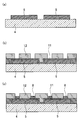
- FIG. 1 is a cross-sectional view showing a main part of an electronic component module 100 according to a first embodiment of the present invention, and shows an arrow AA portion in FIG. 3A to 3C are cross-sectional views showing respective steps applied in the method for manufacturing the electronic component module 100 according to the first embodiment of the present invention.
- 4 (d) to (f) are continuations of FIG. 3, and are cross-sectional views showing respective steps applied in the method of manufacturing the electronic component module 100 according to the first embodiment of the present invention.
- 4 (g) to 4 (i) are continuations of FIG.
- FIG. 1 and 2 show a joined state between a substrate and an electronic component element in the electronic component module 100 according to the first embodiment of the present invention.
- FIG. 2 shows a cross section taken along the line AA in FIG.
- the electronic component module 100 includes a substrate 1.
- a substrate 1 As the material of the substrate 1, for example, ceramic or resin is used.
- a plurality of substrate electrodes 2 are formed on the main surface of the substrate 1.
- Cu or Ag is used as the material of the substrate electrode 2.
- the electronic component module 100 includes an electronic component element 4.
- the electronic component element 4 for example, a semiconductor element or the like is used, and generally there are many rectangular elements.
- a plurality of pad electrodes 5 are formed on the main surface of the electronic component element 4.
- the pad electrode 5 may have any shape, but in the present embodiment, the pad electrode 5 has a rectangular shape in accordance with the shape of the electronic component element 4.
- Al or the like is used as the material of the pad electrode 5.
- an insulating film 6 is formed on the main surface of the electronic component element 4 by providing an opening in the pad electrode 5 portion.
- SiN or the like is used as the material of the insulating film 6.
- a columnar electrode 7 is formed on the center of the pad electrode 5 of the electronic component element 4.
- the columnar electrode 7 has a cylindrical shape.
- the shape of the columnar electrode 7 is not limited to this, and may be a polygonal column shape, a truncated cone shape, a polygonal truncated cone shape, or the like.
- Cu is used as the material of the columnar electrode 7.
- metals other than Cu such as Ni, Pt, and Pd, may be used.
- annular electrode 8 is formed on the pad electrode 5 of the electronic component element 4 so as to surround the columnar electrode 7.
- the planar shape of the annular electrode 8 is an annular shape. However, it is not limited to an annular shape, and may be a rectangular shape.
- the annular electrode 8 protrudes from the surface of the pad electrode.
- Cu is used as the material of the annular electrode 8.
- metals other than Cu such as Ni, Pt, and Pd, may be used.
- solder bumps 9 are provided on the columnar electrodes 7.
- the electronic component element 4 is flip-chip mounted on the substrate 1 by bonding solder bumps 9 provided on the columnar electrode 7 to the substrate electrode 2 of the substrate 1.
- the electronic component module 100 is filled with a resin 10 between the substrate 1 and the electronic component element 4 in order to increase the bonding strength between the substrate 1 and the electronic component element 4.
- the resin 10 is not filled, assuming that the board is reused by electronic component repair.
- the annular electrode 8 surrounding the columnar electrode 7 is formed on the pad electrode 5
- the molten solder is generated when solder splash occurs.
- a path reaching the adjacent solder bump 9 is long, and a short circuit with the adjacent solder bump 9 is suppressed.
- the columnar electrode 7 and the annular electrode 8 are formed of a metal, the effect of preventing the solder from flowing out is increased as compared with the case where the columnar electrode 7 and the annular electrode 8 are formed of SiN or the like having a function of repelling conventional solder.
- solder bumps 9 are provided on the columnar electrodes 7 formed on the pad electrodes 5, the arrangement positions of the solder bumps 9 are accurately controlled. Therefore, a plurality of solder bumps 9 can be formed adjacent to each other at a narrow pitch.
- the substrate 1 is composed of a multilayer substrate on which an inner layer conductor for wiring and an inner layer conductor for capacitance formation are formed, and formed external terminals are formed on the surface thereof.
- a via hole conductor is connected between the substrate electrode 2 on which the electronic component element 4 is mounted and the external terminal electrode.
- a chip capacitor or the like may be mounted on a substrate electrode 2 different from the substrate electrode 2 on which the electronic component element 4 of the substrate 1 is mounted. Further, it may be built in the substrate with a chip capacitor or the like connected to the inner layer conductor of the substrate 1.
- an electronic component element 4 such as a semiconductor element in which a plurality of pad electrodes 5 made of Al or the like are formed in advance is prepared.
- a seed layer 11 that forms the basis for forming the columnar electrode 7 and the annular electrode 8 is formed on the electronic component element 4 by vapor deposition or sputtering.
- Ti or Cu is used as the material of the seed layer 11.
- a resist 12 for forming the annular electrode 8 is formed.
- SiN, SiO 2 or the like is used as the material of the resist 12.
- the resist 12 is first applied on the entire surface of the seed layer 11. Subsequently, the resist 12 is covered with a mask (not shown) in which a portion where the annular electrode 16 is to be formed is punched, and exposure is performed by irradiating ultraviolet rays in the manner of photolithography. Subsequently, the mask is removed and development processing is performed with a developer. By the development process, an opening having an exposed shape, that is, a planar shape of the annular electrode 8 (for example, an annular shape) is formed in the resist 12.
- an annular electrode 8 is formed in the opening of the resist 12 by performing a plating process.
- the resist 12 is peeled and removed, whereby the annular electrode 8 is completed on the pad electrode 5 via the seed layer 11 as shown in FIG.
- columnar electrodes 7 and solder bumps 9 are formed.
- a resist 13 is applied again on the seed layer 11 on which the annular electrode 8 is formed. Subsequently, the resist 13 is covered with a mask in which a portion where the columnar electrode 7 is to be formed is punched, and exposure is performed by irradiating ultraviolet rays in the manner of photolithography. Subsequently, the mask is removed and development processing is performed with a developer. By the development process, as shown in FIG. 4E, an opening having an exposed shape, that is, a planar shape (for example, a circle) of the columnar electrode 7 is formed in the resist 13.
- the remaining resist 13 is peeled and removed, and then the remaining seed layer 11 is removed by etching.
- the solder layer 9 ' is formed on the substantially spherical solder bumps 9 by performing a reflow process.
- solder bumps 9 are joined to the substrate electrode 2 by reflow, and the electronic component element 4 is flip-chip mounted on the substrate 1.
- the resin 10 is filled between the substrate 2 and the electronic component element 4 to complete the electronic component module 100 according to the present embodiment.
- 5 (g) to (i) the seed layer portions of the columnar electrode 7 and the annular electrode 8 are illustrated, but the illustration is omitted in FIG. 1 showing the completed state.
- the structure of the electronic component module 100 according to the first embodiment of the present invention and an example of the manufacturing method have been described above.
- the content of the present invention is not limited to the content described above, and various modifications can be made in accordance with the gist of the invention.
- the columnar electrode 7 and the annular electrode 8 may be formed by a method such as vapor deposition or printing instead of photolithography.
- the interface between the metal electrode and solder may be alloyed to increase the bonding strength.
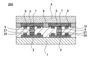
- FIG. 6 shows a main part of an electronic component module 200 according to the second embodiment of the present invention.
- the columnar electrode 27 and the annular electrode 28 were also formed on the substrate electrode 2 of the substrate 1.
- Other configurations are the same as those of the electronic component module 100 according to the first embodiment described above.
- FIG. 7 shows a main part of an electronic component module 300 according to the third embodiment of the present invention.
- the height h1 of the annular electrode 18 is set higher than the height h2 of the columnar electrode 7.
- the annular electrode 18 comes into contact with the substrate electrode 2, and the space 13 is formed by the pad electrode 5, the annular electrode 18, and the substrate electrode 2, and the resin 13 is not filled in the space 13.
- Other configurations of the electronic component module 300 are based on the electronic component module 100 according to the first embodiment described above.
- solder splash does not occur. Even if solder splash occurs, the molten solder does not leak out beyond the annular electrode 18 because it is surrounded by the annular electrode 18.
- Substrate 2 Substrate electrode 4: Electronic component element (semiconductor element, etc.) 5: Pad electrode 6: Insulating film 7: Columnar electrode 8, 18: Ring electrode 9: Solder bump 9 ′: Solder layer 10: Resin 11: Seed layer 12, 13: Resist 27: Columnar (formed on substrate electrode) Electrode 28: annular electrode 100, 200, 300 (formed on substrate electrode): electronic component module
Landscapes
- Engineering & Computer Science (AREA)
- Computer Hardware Design (AREA)
- Microelectronics & Electronic Packaging (AREA)
- Power Engineering (AREA)
- Manufacturing & Machinery (AREA)
- Physics & Mathematics (AREA)
- Condensed Matter Physics & Semiconductors (AREA)
- General Physics & Mathematics (AREA)
- Wire Bonding (AREA)
Abstract
はんだスプラッシュの発生を抑制した電子部品モジュールを提供する。 電子部品モジュール100は、複数の基板電極2が形成された基板1上に、複数のパッド電極5が形成された電子部品素子4が対向して配置され、基板電極2とパッド電極5がはんだバンプにより接続されたものからなり、パッド電極上に柱状電極7が形成され、柱状電極7上にはんだバンプ9が設けられるとともに、パッド電極5上に、柱状電極7を囲むように、環状電極8が形成されたものからなる。
Description
本発明は、基板上に電子部品素子がフリップチップ実装された電子部品モジュールに関し、さらに詳しくは、基板と電子部品素子の接合構造に改良が加えられた電子部品モジュールに関する。
また、本発明は、上記電子部品モジュールに使用するのに適した電子部品素子に関する。
近年、電子機器の小型化、高機能化により、半導体などの電子部品素子の基板への高密度実装が要求されている。その要求に応える方法として、フリップチップ実装が広く用いられている。このフリップチップ実装は、一般的には、電子部品素子側にはんだバンプを設け、リフローにより電子部品素子を基板にはんだ接合し、さらに接合力強化のために、基板と電子部品素子の間に樹脂を充填するようにしている。
このように、基板に電子部品素子をフリップチップ実装した電子部品モジュールは、さらに、より大きな実装基板にリフローはんだにより実装されることが多い。しかしながら、電子部品モジュールを実装基板に実装する場合、リフロー加熱により、基板と電子部品素子を接合しているはんだが再溶融し、溶融したはんだが、電子部品素子と基板との接合面に沿って流出し、隣接した他のはんだバンプと電気的に短絡してしまう可能性があった。
これを防止した電子部品モジュールが、特許文献1(特開2004-47637号公報)に開示されている。
図8に、特許文献1に開示された電子部品モジュール(半導体パッケージ)400を示す。
電子部品モジュール400は、基板101を備える。基板101の主面上には、複数の基板電極102が形成されている。また、基板101の主面上には、基板電極102部分を除いて、はんだレジスト103が形成されている。
また、電子部品モジュール400は、電子部品素子(半導体素子)104を備える。電子部品素子104の主面上には、複数のパッド電極105が形成されている。また、電子部品素子104の主面上には、パッド電極105部分を除いて、絶縁膜106が形成されている。そして、絶縁膜106には、パッド電極105を囲むように、突起状のはんだダム106aが形成されている。はんだダム106aは、電子部品モジュール400を実装基板(図示せず)に実装するときに、溶融したはんだが流出するのを防止する機能をはたす。
そして、電子部品素子104は、パッド電極105上に設けられたはんだバンプ109を、基板101の基板電極102に接合することにより、基板101にフリップチップ実装されている。
さらに、電子部品モジュール400は、基板101と電子部品素子104の接合強度を大きくするために、基板101と電子部品素子104との間に、樹脂110が充填されている。
しかしながら、上述した従来の電子部品モジュール400には、次のような問題があった。
すなわち、電子部品素子104の絶縁膜106に、はんだ流出防止のための突起状のはんだダム106aを形成するためには、ある程度の大きな面積を必要とするため、近時の、小型化、高密度化が要求される電子部品モジュールにおいては、絶縁膜106上にはんだダム106aを形成するための面積を確保することができないという問題があった。
また、一般的に、電子部品素子104に形成する絶縁膜106は、SiNなどで形成する場合が多いが、SiNなどからなる絶縁膜106およびはんだダム106aは、はんだを弾く傾向があるため、溶融したはんだバンプ109のはんだが、絶縁膜106上に留まらず、はんだダム106aを超えて流出しやすいという問題があった。そして、はんだダム106aを超えて流出したはんだが、隣接するはんだバンプ109と電気的に短絡してしまう場合があるという問題があった。
そこで、本発明の目的は、狭ピッチにはんだバンプが形成されていたとしても、はんだの流出を防止することができる構造を備えた、電子部品モジュールを提供することである。
その手段として、本発明の電子部品モジュールは、複数の基板電極が形成された基板上に、複数のパッド電極を有する電子部品素子が前記基板電極と前記パッド電極とが対向するように配置され、基板電極とパッド電極とがはんだバンプを介して電気的に接続されてなる電子部品モジュールにおいて、パッド電極上に形成された柱状電極と、柱状電極の先端に形成されたはんだバンプと、柱状電極を囲むようにパッド電極上に形成された環状電極とを備えている、ものとした。かかる構造とすることにより、本発明の電子部品モジュールは、はんだの流出を確実に防止することができる。
なお、環状電極は、パッド電極の表面から突出するように形成されていることが好ましい。この場合には、はんだの流出を防止する機能が高くなる。
また、基板と電子部品素子の間に、樹脂を充填するようにしても良い。この場合には、基板と電子部品素子の接合強度をより大きくすることができる。
また、環状電極の高さが柱状電極の高さよりも高く、環状電極が基板電極に当接してしても良い。この場合には、環状電極によって柱状電極およびはんだバンプが完全に囲まれることになり、はんだの流出を完全に防止することができる。
また、基板電極に、別途、柱状電極および環状電極の少なくとも一方を設けるようにしても良い。この場合には、基板側においてはんだが流出する場合にも、はんだの流出を抑制することができる。
また、本発明の電子部品素子は、実装面を有する電子部品本体と、実装面上に形成された複数のパッド電極と、パッド電極上に形成された柱状電極と、柱状電極の先端に形成されたはんだバンプと、柱状電極を囲むようにパッド電極上に形成された環状電極とを備えた構造とした。かかる構造とすることにより、本発明の電子部品素子は、基板に上記はんだバンプを使ってフリップチップ実装して電子部品モジュールを製造し、その電子部品モジュールを実装基板に実装する場合に、リフロー加熱によりはんだが再溶融しても、溶融したはんだが流出するのを確実に防止することができる。
本発明の電子部品モジュールは、パッド電極上に金属製の環状電極を形成したものであるため、特許文献1に開示された従来技術のように、SiNなど、はんだを弾く性質をもった絶縁膜にはんだダムを形成したものに比べて、はんだ流出を防止する機能が大きく向上している。
また、本発明の電子部品モジュールは、はんだバンプが、パッド電極上に直接に設けられるのではなく、パッド電極上に形成された柱状電極上に設けられているため、各はんだバンプの配置位置をより正確に制御することができる。したがって、複数のはんだバンプを、狭いピッチで隣接して形成することができる。
さらに、本発明の電子部品モジュールは、はんだバンプが、パッド電極上に形成された柱状電極上に設けられており、はんだバンプとパッド電極との間に一定の距離が設けられている。そのため、万一、はんだスプラッシュが発生しても、溶融したはんだは、柱状電極の側面、パッド電極の表面、環状電極を経由しなければ、隣接するパッド電極やはんだバンプに到達することができない。このように、はんだの経由経路が長くなっていることによっても、はんだ流出を防止する機能が大きく向上している。
以下、本発明の実施形態について、図面を参照しながら説明する。
(第1実施形態)
図1および図2に、本発明の第1実施形態にかかる電子部品モジュール100における基板と電子部品素子との接合状態を示す。ただし、図2は、図1の矢印A-A部分の断面を示している。
図1および図2に、本発明の第1実施形態にかかる電子部品モジュール100における基板と電子部品素子との接合状態を示す。ただし、図2は、図1の矢印A-A部分の断面を示している。
電子部品モジュール100は、基板1を備える。基板1の材質には、たとえば、セラミックや樹脂などが用いられる。基板1の主面上には、複数の基板電極2が形成されている。基板電極2の材質には、たとえば、CuやAgなどが用いられる。
また、電子部品モジュール100は、電子部品素子4を備える。電子部品素子4としては、たとえば、半導体素子などが用いられ、一般的には矩形状のものが多い。電子部品素子4の主面上には、複数のパッド電極5が形成されている。パッド電極5の形状は問わないが、本実施形態では、電子部品素子4の形状に合わせて矩形状とした。パッド電極5の材質には、たとえば、Alなどが用いられる。また、電子部品素子4の主面上には、パッド電極5部分に開口を設けて、絶縁膜6が形成されている。絶縁膜6の材質には、たとえば、SiNなどが用いられる。
そして、電子部品素子4のパッド電極5の中心部上には、柱状電極7が形成されている。本実施形態においては、柱状電極7の形状を円柱状とした。ただし、柱状電極7の形状はこれには限定されず、多角柱状、円錐台状、多角錐台状などであっても良い。柱状電極7の材質には、たとえば、Cuが用いられる。ただし、Ni、Pt、Pdなど、Cu以外の金属であっても良い。
また、電子部品素子4のパッド電極5上には、柱状電極7を囲むように、環状電極8が形成されている。本実施形態においては、環状電極8の平面形状を円環状とした。ただし、円環状には限られず、矩形環状であっても良い。環状電極8は、パッド電極の表面から突出している。環状電極8の材質には、たとえば、Cuが用いられる。ただし、Ni、Pt、Pdなど、Cu以外の金属であっても良い。
そして、柱状電極7上に、はんだバンプ9が設けられている。
電子部品素子4は、柱状電極7上に設けられたはんだバンプ9を、基板1の基板電極2に接合することにより、基板1にフリップチップ実装されている。
さらに、電子部品モジュール100は、基板1と電子部品素子4の接合強度を大きくするために、基板1と電子部品素子4の間に、樹脂10が充填されている。ただし、しかし、電子部品リペアによる基板再利用等を想定して、樹脂10を充填しない場合もある。
以上の構造からなる、本発明の第1実施形態にかかる電子部品モジュール100は、柱状電極7を囲む環状電極8がパッド電極5上に形成されているため、はんだスプラッシュ発生時に、溶融したはんだが隣接するはんだバンプ9に到達する経路が長くなっており、隣接するはんだバンプ9との短絡が抑制されている。さらに、柱状電極7および環状電極8が金属で形成されていることにより、従来のはんだを弾く作用のあるSiNなどで形成した場合に比べて、はんだ流失を防止する効果が高まっている。
さらに、はんだバンプ9が、パッド電極5上に形成された柱状電極7上に設けられているため、各はんだバンプ9の配置位置が正確に制御されている。したがって、複数のはんだバンプ9を、狭いピッチで隣接して形成することができる。
なお、図示しないが、基板1は、配線用内層導体や容量形成用内層導体が形成された多層基板で構成され、その表面には、形成された外部端子が形成されている。電子部品素子4が実装されている基板電極2と外部端子電極の間はビアホール導体で接続されている。
また、基板1の電子部品素子4が実装されている基板電極2とは別の基板電極2にチップコンデンサなどが実装されていてもよい。また、基板1の内層導体にチップコンデンサなどが接続された状態で基板内に内蔵されていてもよい。
次に、図3(a)~図5(i)を参照して、電子部品モジュール100の製造方法の一例について説明する。
まず、図3(a)に示すように、予めAlなどからなる複数のパッド電極5が形成された半導体素子などの電子部品素子4を用意する。
次に、図3(b)に示すように、電子部品素子4上に、柱状電極7や環状電極8を形成の基礎となるシード層11を、蒸着やスパッタリングにより形成する。シード層11の材質には、たとえば、TiやCuを用いる。そして、シード層11を形成した後に、環状電極8を形成するためのレジスト12を形成する。レジスト12の材質には、たとえば、SiN、SiO2などが用いられる。レジスト12は、まずシード層11上の全面に塗布する。続いて、レジスト12上に、環状電極16を形成する部分を打ち抜きにしたマスク(図示せず)を覆せ、フォトリソグラフィの要領で、紫外線を照射して露光を行う。続いて、マスクを外し、現像液により現像処理を行う。現像処理により、レジスト12には、露光された形、すなわち環状電極8の平面形状(たとえば円環状)をした開口が形成される。
次に、図3(c)に示すように、めっき処理を施すことにより、レジスト12の開口部に環状電極8を形成する。
次に、レジスト12を剥離除去することにより、図4(d)に示すように、パッド電極5上に、シード層11を介して、環状電極8が完成する。
続いて、柱状電極7およびはんだバンプ9の形成を行う。
まず、図示しないが、環状電極8が形成されたシード層11上に、再度、レジスト13を塗布する。続いて、レジスト13上に、柱状電極7を形成する部分を打ち抜きにしたマスクを覆せ、フォトリソグラフィの要領で、紫外線を照射して露光を行う。続いて、マスクを外し、現像液により現像処理を行う。現像処理により、図4(e)に示すように、レジスト13には、露光された形、すなわち柱状電極7の平面形状(たとえば円形)をした開口が形成される。
次に、図4(f)に示すように、めっき処理を施すことにより、レジスト13の開口部に、まず、柱状電極7を形成し、続いてはんだバンプ9のもととなる、はんだめっき層9’を形成する。
次に、図5(g)に示すように、残ったレジスト13を剥離除去し、続いて、エッチング処理により残ったシード層11を剥離除去する。
次に、図5(h)に示すように、リフロー処理を施すことにより、はんだ層9’を、略球状のはんだバンプ9に形成する。
最後に、図5(i)に示すように、基板電極2にはんだバンプ9をリフローにより接合し、基板1に電子部品素子4をフリップチップ実装し、続いて、基板1と電子部品素子4の接合強度を高めるため、基板2と電子部品素子4の間に樹脂10を充填して、本実施形態にかかる電子部品モジュール100を完成させる。なお、図5(g)~(i)においては、柱状電極7および環状電極8のシード層部分を図示しているが、完成状態を示す図1においては、図示を省略している。
以上、本発明の第1実施形態にかかる電子部品モジュール100の構造、および製造方法の一例について説明した。しかしながら、本発明の内容が上述した内容に限定されることはなく、発明の主旨に沿って、種々の変更をなすことができる。
たとえば、柱状電極7や環状電極8の形成は、フォトリソグラフィに代えて、蒸着や印刷などの方法によっても良い。
また、金属製の電極とはんだとの界面を合金化させ、接合強度を高めるようにしても良い。
また、パッド電極5上にその表面から突出するように環状電極8を設けているが、パッド電極5の表面に凹溝を形成するような環状電極にしても、はんだ流出を防止する機能をはたす。
(第2実施形態)
図6に、本発明の第2実施形態にかかる電子部品モジュール200の要部を示す。
(第2実施形態)
図6に、本発明の第2実施形態にかかる電子部品モジュール200の要部を示す。
電子部品モジュール200は、基板1の基板電極2上にも、柱状電極27および環状電極28を形成した。他の構成は、上述した第1実施形態にかかる電子部品モジュール100に準じた。
本実施形態にかかる電子部品モジュール200においては、基板2側においてはんだが流出した場合にも、はんだの流出を抑制することができる。
(第3実施形態)
図7に、本発明の第3実施形態にかかる電子部品モジュール300の要部を示す。
(第3実施形態)
図7に、本発明の第3実施形態にかかる電子部品モジュール300の要部を示す。
電子部品モジュール300においては、環状電極18の高さh1を、柱状電極7の高さh2よりも高くした。この結果、環状電極18が基板電極2に当接し、パッド電極5と環状電極18と基板電極2とで空間13が形成され、空間13内には樹脂10は充填されない。電子部品モジュール300の他の構成は、上述した第1実施形態にかかる電子部品モジュール100に準じた。
電子部品モジュール300においては、柱状電極7およびはんだバンプ9が環状電極18で完全に囲まれ、空間13が形成されているため、はんだスプラッシュが発生しない。仮にはんだスプラッシュが発生しても、環状電極18に囲まれているため、溶融したはんだが環状電極18を超えて周辺に漏れ出すことはない。
1:基板
2:基板電極
4:電子部品素子(半導体素子など)
5:パッド電極
6:絶縁膜
7:柱状電極
8、18:環状電極
9:はんだバンプ
9’:はんだ層
10:樹脂
11:シード層
12、13:レジスト
27:(基板電極に形成された)柱状電極
28:(基板電極に形成された)環状電極
100、200、300:電子部品モジュール
2:基板電極
4:電子部品素子(半導体素子など)
5:パッド電極
6:絶縁膜
7:柱状電極
8、18:環状電極
9:はんだバンプ
9’:はんだ層
10:樹脂
11:シード層
12、13:レジスト
27:(基板電極に形成された)柱状電極
28:(基板電極に形成された)環状電極
100、200、300:電子部品モジュール
Claims (7)
- 複数の基板電極が形成された基板上に、複数のパッド電極を有する電子部品素子が前記基板電極と前記パッド電極とが対向するように配置され、前記基板電極と前記パッド電極とがはんだバンプを介して電気的に接続されてなる電子部品モジュールにおいて、
前記パッド電極上に形成された柱状電極と、
前記柱状電極の先端に形成されたはんだバンプと、
前記柱状電極を囲むように前記パッド電極上に形成された環状電極とを備えている、
ことを特徴とする電子部品モジュール。 - 前記環状電極は、前記パッド電極の表面から突出するように形成されていることを特徴とする、請求項1に記載された電子部品モジュール。
- 前記基板と前記電子部品素子の間に樹脂が充填されていることを特徴とする、請求項1または2に記載された電子部品モジュール。
- 前記環状電極の高さが前記柱状電極の高さよりも高く、前記環状電極が前記基板電極に当接していることを特徴とする、請求項3に記載された電子部品モジュール。
- 前記パッド電極、前記環状電極、および前記基板電極で構成される空間を除いて、前記基板と前記電子部品素子との間に樹脂が充填されていることを特徴とする、請求項4に記載された電子部品モジュール。
- 前記基板電極に、前記柱状電極および前記環状電極の少なくとも一方が設けられていることを特徴とする、請求項1ないし5のいずれか1項に記載された電子部品モジュール。
- 実装面を有する電子部品本体と、前記実装面上に形成された複数のパッド電極と、前記パッド電極上に形成された柱状電極と、前記柱状電極の先端に形成されたはんだバンプと、前記柱状電極を囲むように前記パッド電極上に形成された環状電極とを備えたことを特徴とする電子部品素子。
Priority Applications (2)
| Application Number | Priority Date | Filing Date | Title |
|---|---|---|---|
| JP2012554816A JP5370599B2 (ja) | 2011-01-26 | 2012-01-25 | 電子部品モジュールおよび電子部品素子 |
| CN201280005003.3A CN103299410B (zh) | 2011-01-26 | 2012-01-25 | 电子元器件模块及电子元器件单元 |
Applications Claiming Priority (2)
| Application Number | Priority Date | Filing Date | Title |
|---|---|---|---|
| JP2011-013711 | 2011-01-26 | ||
| JP2011013711 | 2011-01-26 |
Publications (1)
| Publication Number | Publication Date |
|---|---|
| WO2012102303A1 true WO2012102303A1 (ja) | 2012-08-02 |
Family
ID=46580868
Family Applications (1)
| Application Number | Title | Priority Date | Filing Date |
|---|---|---|---|
| PCT/JP2012/051544 WO2012102303A1 (ja) | 2011-01-26 | 2012-01-25 | 電子部品モジュールおよび電子部品素子 |
Country Status (3)
| Country | Link |
|---|---|
| JP (1) | JP5370599B2 (ja) |
| CN (1) | CN103299410B (ja) |
| WO (1) | WO2012102303A1 (ja) |
Cited By (6)
| Publication number | Priority date | Publication date | Assignee | Title |
|---|---|---|---|---|
| JP2016012704A (ja) * | 2014-06-30 | 2016-01-21 | インターナショナル・ビジネス・マシーンズ・コーポレーションInternational Business Machines Corporation | 接合構造体、接合方法、基板構造体、無線モジュールおよび無線通信装置(伝送経路上を避けて設計された充填材料構造) |
| WO2017221587A1 (ja) * | 2016-06-20 | 2017-12-28 | ソニー株式会社 | 基板装置、電子機器及び基板装置の製造方法 |
| JP2019507905A (ja) * | 2016-02-18 | 2019-03-22 | アップル インコーポレイテッドApple Inc. | マイクロドライバ及びマイクロledのためのバックプレーン構造及びプロセス |
| JP2019161108A (ja) * | 2018-03-15 | 2019-09-19 | 日亜化学工業株式会社 | 発光装置、発光素子、及び、発光素子の製造方法 |
| JP2020120079A (ja) * | 2019-01-28 | 2020-08-06 | 京セラ株式会社 | 配線基板 |
| WO2020175570A1 (ja) * | 2019-02-28 | 2020-09-03 | 新田ゼラチン株式会社 | 脳機能調整剤、およびこれを含む飲食品 |
Families Citing this family (2)
| Publication number | Priority date | Publication date | Assignee | Title |
|---|---|---|---|---|
| CN106847962A (zh) * | 2016-12-07 | 2017-06-13 | 上海锐吉电子科技有限公司 | 单电池片并联二极管的光伏组件 |
| KR20200032361A (ko) * | 2018-09-18 | 2020-03-26 | 삼성전기주식회사 | Mems 디바이스 |
Citations (3)
| Publication number | Priority date | Publication date | Assignee | Title |
|---|---|---|---|---|
| JP2006245289A (ja) * | 2005-03-03 | 2006-09-14 | Casio Micronics Co Ltd | 半導体装置及び実装構造体 |
| JP2006344672A (ja) * | 2005-06-07 | 2006-12-21 | Fujitsu Ltd | 半導体チップとそれを用いた半導体装置 |
| WO2007080863A1 (ja) * | 2006-01-16 | 2007-07-19 | Nec Corporation | 半導体装置、該半導体装置を実装するプリント配線基板、及びそれらの接続構造 |
Family Cites Families (11)
| Publication number | Priority date | Publication date | Assignee | Title |
|---|---|---|---|---|
| KR100216839B1 (ko) * | 1996-04-01 | 1999-09-01 | 김규현 | Bga 반도체 패키지의 솔더 볼 랜드 메탈 구조 |
| JP2001053111A (ja) * | 1999-08-10 | 2001-02-23 | Matsushita Electric Works Ltd | フリップチップ実装構造 |
| JP4483131B2 (ja) * | 2001-05-29 | 2010-06-16 | パナソニック株式会社 | 実装構造体及びその実装方法 |
| JP4350366B2 (ja) * | 2002-12-24 | 2009-10-21 | パナソニック株式会社 | 電子部品内蔵モジュール |
| US7230339B2 (en) * | 2003-03-28 | 2007-06-12 | Intel Corporation | Copper ring solder mask defined ball grid array pad |
| JP2005079499A (ja) * | 2003-09-03 | 2005-03-24 | Seiko Epson Corp | 半導体装置、半導体モジュール、電子機器および半導体装置の製造方法 |
| TWI222192B (en) * | 2003-09-04 | 2004-10-11 | Advanced Semiconductor Eng | Substrate with net structure |
| KR100555706B1 (ko) * | 2003-12-18 | 2006-03-03 | 삼성전자주식회사 | 미세 솔더볼 구현을 위한 ubm 및 이를 이용한 플립칩패키지 방법 |
| KR101134168B1 (ko) * | 2005-08-24 | 2012-04-09 | 삼성전자주식회사 | 반도체 칩 및 그 제조 방법과, 그를 이용한 표시 패널 및그 제조 방법 |
| CN100573857C (zh) * | 2006-07-27 | 2009-12-23 | 南茂科技股份有限公司 | 影像感测晶片与玻璃基板的结合构造及其制造方法 |
| JP2009099730A (ja) * | 2007-10-16 | 2009-05-07 | Phoenix Precision Technology Corp | パッケージ基板の半田ボール配置側表面構造およびその製造方法 |
-
2012
- 2012-01-25 WO PCT/JP2012/051544 patent/WO2012102303A1/ja active Application Filing
- 2012-01-25 JP JP2012554816A patent/JP5370599B2/ja active Active
- 2012-01-25 CN CN201280005003.3A patent/CN103299410B/zh active Active
Patent Citations (3)
| Publication number | Priority date | Publication date | Assignee | Title |
|---|---|---|---|---|
| JP2006245289A (ja) * | 2005-03-03 | 2006-09-14 | Casio Micronics Co Ltd | 半導体装置及び実装構造体 |
| JP2006344672A (ja) * | 2005-06-07 | 2006-12-21 | Fujitsu Ltd | 半導体チップとそれを用いた半導体装置 |
| WO2007080863A1 (ja) * | 2006-01-16 | 2007-07-19 | Nec Corporation | 半導体装置、該半導体装置を実装するプリント配線基板、及びそれらの接続構造 |
Cited By (12)
| Publication number | Priority date | Publication date | Assignee | Title |
|---|---|---|---|---|
| JP2016012704A (ja) * | 2014-06-30 | 2016-01-21 | インターナショナル・ビジネス・マシーンズ・コーポレーションInternational Business Machines Corporation | 接合構造体、接合方法、基板構造体、無線モジュールおよび無線通信装置(伝送経路上を避けて設計された充填材料構造) |
| US9780442B2 (en) | 2014-06-30 | 2017-10-03 | International Business Machines Corporation | Wireless communication device with joined semiconductors |
| US10090586B2 (en) | 2014-06-30 | 2018-10-02 | International Business Machines Corporation | Wireless communication device with joined semiconductors |
| JP2019507905A (ja) * | 2016-02-18 | 2019-03-22 | アップル インコーポレイテッドApple Inc. | マイクロドライバ及びマイクロledのためのバックプレーン構造及びプロセス |
| US10546796B2 (en) | 2016-02-18 | 2020-01-28 | Apple Inc. | Backplane structure and process for microdriver and micro LED |
| JP2020052404A (ja) * | 2016-02-18 | 2020-04-02 | アップル インコーポレイテッドApple Inc. | マイクロドライバ及びマイクロledのためのバックプレーン構造及びプロセス |
| WO2017221587A1 (ja) * | 2016-06-20 | 2017-12-28 | ソニー株式会社 | 基板装置、電子機器及び基板装置の製造方法 |
| US10892241B2 (en) | 2016-06-20 | 2021-01-12 | Sony Corporation | Substrate device, electronic apparatus, and method for manufacturing substrate device |
| JP2019161108A (ja) * | 2018-03-15 | 2019-09-19 | 日亜化学工業株式会社 | 発光装置、発光素子、及び、発光素子の製造方法 |
| JP2020120079A (ja) * | 2019-01-28 | 2020-08-06 | 京セラ株式会社 | 配線基板 |
| JP7211110B2 (ja) | 2019-01-28 | 2023-01-24 | 京セラ株式会社 | 配線基板 |
| WO2020175570A1 (ja) * | 2019-02-28 | 2020-09-03 | 新田ゼラチン株式会社 | 脳機能調整剤、およびこれを含む飲食品 |
Also Published As
| Publication number | Publication date |
|---|---|
| CN103299410B (zh) | 2016-01-27 |
| JPWO2012102303A1 (ja) | 2014-06-30 |
| JP5370599B2 (ja) | 2013-12-18 |
| CN103299410A (zh) | 2013-09-11 |
Similar Documents
| Publication | Publication Date | Title |
|---|---|---|
| JP5370599B2 (ja) | 電子部品モジュールおよび電子部品素子 | |
| US8693211B2 (en) | Wiring substrate and semiconductor device | |
| KR100921919B1 (ko) | 반도체 칩에 형성되는 구리기둥-주석범프 및 그의 형성방법 | |
| KR101910198B1 (ko) | 반도체 장치, 반도체 장치의 제조 방법 및 배선 기판의 제조 방법 | |
| CN106098667B (zh) | 半导体器件 | |
| US9953960B2 (en) | Manufacturing process of wafer level chip package structure having block structure | |
| JP2005109496A (ja) | プリ半田構造を形成するための半導体パッケージ基板及びプリ半田構造が形成された半導体パッケージ基板、並びにこれらの製法 | |
| JP2009105139A (ja) | 配線基板及びその製造方法と半導体装置 | |
| JP2008218505A (ja) | 基板およびその製造方法、半導体パッケージおよびその製造方法、並びに半導体装置およびその製造方法 | |
| US20090102050A1 (en) | Solder ball disposing surface structure of package substrate | |
| US7928559B2 (en) | Semiconductor device, electronic component module, and method for manufacturing semiconductor device | |
| US9559076B2 (en) | Package having substrate with embedded metal trace overlapped by landing pad | |
| US7149091B2 (en) | Electronic circuit device | |
| US7544599B2 (en) | Manufacturing method of solder ball disposing surface structure of package substrate | |
| JP6473002B2 (ja) | バンプ付きプリント配線板 | |
| KR100713912B1 (ko) | 웨이퍼 레벨 공정을 이용한 플립칩 패키지 및 그 제조방법 | |
| JP2013211497A (ja) | 部品接合構造 | |
| JP3972211B2 (ja) | 半導体装置及びその製造方法 | |
| WO2020213133A1 (ja) | 半導体装置 | |
| US9735132B1 (en) | Semiconductor package | |
| JP2016178177A (ja) | 配線基板及び電子部品装置と電子部品装置の製造方法 | |
| KR20160032524A (ko) | 인쇄회로기판 및 그 제조방법 | |
| JP2019186345A (ja) | 配線構造体および電子部品 | |
| JP4906563B2 (ja) | 半導体装置及び配線基板、並びにそれらの製造方法 | |
| JP2009081153A (ja) | 半導体装置及び半導体装置を実装した回路装置 |
Legal Events
| Date | Code | Title | Description |
|---|---|---|---|
| 121 | Ep: the epo has been informed by wipo that ep was designated in this application |
Ref document number: 12738801 Country of ref document: EP Kind code of ref document: A1 |
|
| ENP | Entry into the national phase |
Ref document number: 2012554816 Country of ref document: JP Kind code of ref document: A |
|
| NENP | Non-entry into the national phase |
Ref country code: DE |
|
| 122 | Ep: pct application non-entry in european phase |
Ref document number: 12738801 Country of ref document: EP Kind code of ref document: A1 |