WO2012090986A1 - 電子部品 - Google Patents
電子部品 Download PDFInfo
- Publication number
- WO2012090986A1 WO2012090986A1 PCT/JP2011/080164 JP2011080164W WO2012090986A1 WO 2012090986 A1 WO2012090986 A1 WO 2012090986A1 JP 2011080164 W JP2011080164 W JP 2011080164W WO 2012090986 A1 WO2012090986 A1 WO 2012090986A1
- Authority
- WO
- WIPO (PCT)
- Prior art keywords
- electrode
- electronic component
- surface electrode
- insulating substrate
- external electrode
- Prior art date
- Legal status (The legal status is an assumption and is not a legal conclusion. Google has not performed a legal analysis and makes no representation as to the accuracy of the status listed.)
- Ceased
Links
Images







Classifications
-
- H—ELECTRICITY
- H01—ELECTRIC ELEMENTS
- H01G—CAPACITORS; CAPACITORS, RECTIFIERS, DETECTORS, SWITCHING DEVICES, LIGHT-SENSITIVE OR TEMPERATURE-SENSITIVE DEVICES OF THE ELECTROLYTIC TYPE
- H01G4/00—Fixed capacitors; Processes of their manufacture
- H01G4/30—Stacked capacitors
-
- H—ELECTRICITY
- H01—ELECTRIC ELEMENTS
- H01G—CAPACITORS; CAPACITORS, RECTIFIERS, DETECTORS, SWITCHING DEVICES, LIGHT-SENSITIVE OR TEMPERATURE-SENSITIVE DEVICES OF THE ELECTROLYTIC TYPE
- H01G2/00—Details of capacitors not covered by a single one of groups H01G4/00-H01G11/00
- H01G2/02—Mountings
- H01G2/06—Mountings specially adapted for mounting on a printed-circuit support
-
- H—ELECTRICITY
- H01—ELECTRIC ELEMENTS
- H01G—CAPACITORS; CAPACITORS, RECTIFIERS, DETECTORS, SWITCHING DEVICES, LIGHT-SENSITIVE OR TEMPERATURE-SENSITIVE DEVICES OF THE ELECTROLYTIC TYPE
- H01G4/00—Fixed capacitors; Processes of their manufacture
- H01G4/002—Details
- H01G4/018—Dielectrics
- H01G4/06—Solid dielectrics
- H01G4/08—Inorganic dielectrics
- H01G4/12—Ceramic dielectrics
-
- H—ELECTRICITY
- H01—ELECTRIC ELEMENTS
- H01G—CAPACITORS; CAPACITORS, RECTIFIERS, DETECTORS, SWITCHING DEVICES, LIGHT-SENSITIVE OR TEMPERATURE-SENSITIVE DEVICES OF THE ELECTROLYTIC TYPE
- H01G4/00—Fixed capacitors; Processes of their manufacture
- H01G4/002—Details
- H01G4/228—Terminals
-
- H—ELECTRICITY
- H01—ELECTRIC ELEMENTS
- H01G—CAPACITORS; CAPACITORS, RECTIFIERS, DETECTORS, SWITCHING DEVICES, LIGHT-SENSITIVE OR TEMPERATURE-SENSITIVE DEVICES OF THE ELECTROLYTIC TYPE
- H01G4/00—Fixed capacitors; Processes of their manufacture
- H01G4/002—Details
- H01G4/228—Terminals
- H01G4/232—Terminals electrically connecting two or more layers of a stacked or rolled capacitor
-
- H—ELECTRICITY
- H05—ELECTRIC TECHNIQUES NOT OTHERWISE PROVIDED FOR
- H05K—PRINTED CIRCUITS; CASINGS OR CONSTRUCTIONAL DETAILS OF ELECTRIC APPARATUS; MANUFACTURE OF ASSEMBLAGES OF ELECTRICAL COMPONENTS
- H05K1/00—Printed circuits
- H05K1/18—Printed circuits structurally associated with non-printed electric components
-
- H—ELECTRICITY
- H05—ELECTRIC TECHNIQUES NOT OTHERWISE PROVIDED FOR
- H05K—PRINTED CIRCUITS; CASINGS OR CONSTRUCTIONAL DETAILS OF ELECTRIC APPARATUS; MANUFACTURE OF ASSEMBLAGES OF ELECTRICAL COMPONENTS
- H05K3/00—Apparatus or processes for manufacturing printed circuits
- H05K3/30—Assembling printed circuits with electric components, e.g. with resistors
- H05K3/32—Assembling printed circuits with electric components, e.g. with resistors electrically connecting electric components or wires to printed circuits
- H05K3/34—Assembling printed circuits with electric components, e.g. with resistors electrically connecting electric components or wires to printed circuits by soldering
- H05K3/341—Surface mounted components
- H05K3/3431—Leadless components
- H05K3/3442—Leadless components having edge contacts, e.g. leadless chip capacitors, chip carriers
-
- H—ELECTRICITY
- H05—ELECTRIC TECHNIQUES NOT OTHERWISE PROVIDED FOR
- H05K—PRINTED CIRCUITS; CASINGS OR CONSTRUCTIONAL DETAILS OF ELECTRIC APPARATUS; MANUFACTURE OF ASSEMBLAGES OF ELECTRICAL COMPONENTS
- H05K2201/00—Indexing scheme relating to printed circuits covered by H05K1/00
- H05K2201/10—Details of components or other objects attached to or integrated in a printed circuit board
- H05K2201/10613—Details of electrical connections of non-printed components, e.g. special leads
- H05K2201/10621—Components characterised by their electrical contacts
- H05K2201/10636—Leadless chip, e.g. chip capacitor or resistor
-
- Y—GENERAL TAGGING OF NEW TECHNOLOGICAL DEVELOPMENTS; GENERAL TAGGING OF CROSS-SECTIONAL TECHNOLOGIES SPANNING OVER SEVERAL SECTIONS OF THE IPC; TECHNICAL SUBJECTS COVERED BY FORMER USPC CROSS-REFERENCE ART COLLECTIONS [XRACs] AND DIGESTS
- Y02—TECHNOLOGIES OR APPLICATIONS FOR MITIGATION OR ADAPTATION AGAINST CLIMATE CHANGE
- Y02P—CLIMATE CHANGE MITIGATION TECHNOLOGIES IN THE PRODUCTION OR PROCESSING OF GOODS
- Y02P70/00—Climate change mitigation technologies in the production process for final industrial or consumer products
- Y02P70/50—Manufacturing or production processes characterised by the final manufactured product
Definitions
- the present invention relates to an electronic component generally provided with an interposer, which is used when a chip component such as a multilayer ceramic capacitor is mounted on a circuit board.
- the multilayer ceramic capacitor is composed of a rectangular component body that functions as a capacitor, and external electrodes formed at opposite ends of the component body.
- Patent Document 1 in a multilayer ceramic capacitor, an external electrode is directly placed on a mounting land of a circuit board of a mobile terminal, and the mounting land and the external electrode are soldered or the like. It was electrically and physically connected to the circuit board by bonding with a bonding agent.
- Patent Documents 2 and 3 describe that a multilayer ceramic capacitor is not directly mounted on a mounting land.
- an interposer made of an insulating substrate is used.
- the multilayer ceramic capacitor is bonded to the upper electrode of the interposer, and the lower electrode of the interposer is bonded to the mounting electrode of the circuit board.
- the upper surface electrode and the lower surface electrode are electrically connected by a via hole penetrating the interposer.
- JP-A-8-55752 Japanese Unexamined Patent Publication No. 7-111380 JP 2004-134430 A
- the component substrate is overlaid on the support substrate and bonded with a bonding material, and then a solder resist is formed only on the side surface of the component substrate, and solder when mounted on the circuit substrate.
- a solder resist is formed only on the side surface of the component substrate, and solder when mounted on the circuit substrate.
- the solder at the time of mounting wets to the side surface of the support substrate, but does not adhere to the external electrodes of the component substrate, so that the component substrate is not strongly restrained.
- the component board vibrates, it is possible to suppress the vibration from propagating to the circuit board or the like via the support board.
- this structure after bonding the component substrate to the support substrate with a bonding material, it is necessary to form a solder resist only on the side surface of the component substrate, which may increase manufacturing costs.
- the arrangement direction of the lower electrode in the interposer and the arrangement direction of the upper electrode intersect, that is, the arrangement direction of the external electrodes of the multilayer ceramic capacitor and the arrangement of the mounting electrodes on the circuit board of the interposer
- a special structure is used in which the directions intersect. Therefore, the interposer is increased in size, the electrode shape of the interposer is complicated, and the cost may be further increased.
- the object of the present invention is to realize an electronic component that is easy to design and mount, has the same mounting strength and electrical characteristics as a conventional general mounting structure, and can more effectively suppress the generation of vibration noise. There is to do.
- the present invention includes a flat insulating substrate, a first upper surface electrode formed on one main surface of the insulating substrate, a second upper surface electrode, a first lower surface electrode formed on the other main surface of the insulating substrate, A substrate having two lower surface electrodes, a first external electrode and a second external electrode are formed opposite to both ends in the length direction of the main body, the first external electrode is mounted on the first upper surface electrode, and the second external electrode And an electronic component including a chip component on which an electrode is mounted on a second upper surface electrode.
- the substrate is formed on an end surface orthogonal to the one main surface and the other main surface, and connects the first upper surface electrode and the first lower surface electrode, and connects the second upper surface electrode and the second upper surface electrode.
- connection electrode is provided.
- the first upper surface electrode and the first lower surface electrode are separated from each other, and the second upper surface electrode and the second lower surface electrode are separated from each other at substantially the center in the width direction orthogonal to the length direction of the main body of the chip component.
- solder solder
- solder bonding is performed so that a solder fillet is formed at least from the mounting land formed on the circuit board to the connection electrode of the board.
- a fillet By forming a fillet in this way, it is very effective because it can prevent floating when mounting electronic components, secure bonding strength, and visually confirm that soldering is securely performed. is there.
- a large amount of solder may wet the electronic component. If the solder spreads to the center of the end surface of the chip component through the insulating substrate, both ends of the chip component are strongly restrained, and the vibration of the chip component is easily transmitted to the circuit substrate through the insulating substrate. May produce sound.
- the configuration of the present invention is used, even if the solder wets from the electronic component and reaches the first and second external electrodes of the chip component, it adheres most to the corner on the bottom side of the chip component.
- the solder spreads from the corner to the ridge line extending in the direction orthogonal to the main surface, and the solder is restricted from adhering to the vicinity of the center of the external electrode. Thereby, generation
- the electronic component has a structure in which a flat insulating substrate is simply added to the chip component, it is possible to reduce the height and obtain the same bonding strength as the conventional one. In addition, since no special structure is required, it is possible to easily change parts and design.
- the electronic component of the present invention preferably has the following configuration.
- the insulating substrate is provided with a first upper surface electrode and a first lower surface electrode at a position corresponding to the first external electrode of the chip component, and a second upper surface at a position corresponding to the second external electrode of the chip component.
- An electrode and a second bottom electrode are provided.
- the plurality of connection electrodes are formed at the four corners of the insulating substrate.
- the arrangement direction of the first and second external electrodes formed at both ends of the chip component is substantially the same as the arrangement direction of the first and second upper surface electrodes and the first and second lower surface electrodes of the electronic component.
- the connection electrodes are formed at the four corners of the insulating substrate, the connection electrodes are closest to the ridge lines of the first and second external electrodes. As a result, the solder wetted on the first and second upper surface electrodes adheres to the vicinity of the ridge line portion.
- notches are formed at the four corners of the insulating substrate, and a connection electrode is formed on the inner wall surface of the notch.
- connection electrode and the first and second upper surface electrode side ends of the ridge line portions of the first and second external electrodes becomes closer.
- the notch portion when the chip component is mounted on the insulating substrate, at least a part of the notch portion is configured by the outer shape of the chip component when viewed from the direction orthogonal to the one main surface and the other main surface. It is preferable that it exists in the area
- the solder since at least a part of the notch is disposed within the outer shape region of the chip component, even if the solder wets up the connection electrode formed on the notch, the solder is external to the chip component. It can stop near the ridge line part of an electrode, and can suppress that the whole upper surface electrode of an insulating substrate and by extension, the whole length direction both end surface of a chip component spread out.
- the connection electrode and the ridge line portion of the external electrode of the chip component are substantially at the same position, the land on the circuit board that is used when the chip component is directly mounted on the circuit board can be used as it is.
- the notch is preferably formed in an arc shape that swells toward the center side of the insulating substrate when viewed from a direction orthogonal to the one main surface and the other main surface.
- the center side of the insulating substrate With respect to the outer shape of the substrate, that is, the length direction that is the arrangement direction of the first and second upper surface electrodes, and the length that is cut out in the width direction orthogonal to the length direction, the center side of the insulating substrate The distance to be recessed can be made longer. As a result, the distance between the connection electrode and the first and second upper surface electrode side ends of the ridge line portions of the first and second external electrodes is further reduced.
- the insulating substrate is formed with an outer shape smaller than the outer shape of the chip component when viewed from the direction orthogonal to the one main surface and the other main surface when the chip component is mounted. It may be.
- the insulating substrate enters the inside of the outer shape of the chip component, the solder that has wetted the connection electrode is blocked by the bottom surface side of the ridge line portions of the first and second external electrodes of the chip component. Solder adhesion to the vicinity of the center of the first and second external electrodes can be suppressed.
- the position of the ridge line portion of the first and second external electrodes is the bonding position between the electronic component and the circuit board when viewed from the direction orthogonal to the main surface of the insulating substrate, the chip component alone is directly connected to the circuit board.
- An electronic component can be mounted on a mounting land having substantially the same shape as the mounting land to be mounted on. Thereby, an electronic component can be mounted, without enlarging planarly.
- the insulating substrate includes a predetermined position including a position where a perpendicular line dropped from the center of the end portion where the first external electrode and the second external electrode of the chip component are formed intersects the substrate. In the range, you may face directly with respect to the 1st external electrode and the 2nd external electrode.
- the first external electrode and the second external electrode are within a predetermined range including a position where a perpendicular line extending from the center of the end where the first external electrode and the second external electrode of the chip component are formed to the substrate intersects the substrate. Since the insulating substrate directly faces the external electrode, the wet solder can be prevented from reaching the centers of the end faces of the first and second external electrodes. That is, by forming the electrode non-forming portion in the predetermined range of the insulating substrate, it is possible to prevent the wet solder from reaching the centers of the end faces of the first and second external electrodes.
- the first upper surface electrode and the second upper surface electrode on the surface on which the chip component is mounted are arranged from the center of the end where the first external electrode and the second external electrode of the chip component are formed.
- a resist film may be provided in a predetermined range including a position where a perpendicular line dropped on the first upper surface electrode and the second upper surface electrode intersects the substrate.
- the resist film can prevent wet solder from reaching the centers of the end faces of the first and second external electrodes.
- the present invention also provides a flat insulating substrate, a first upper surface electrode formed on one main surface of the insulating substrate, a second upper surface electrode, and a first lower surface electrode formed on the other main surface of the insulating substrate.
- a first external electrode and a second external electrode are formed on the substrate having the second lower surface electrode, opposite to both ends in the longitudinal direction of the main body, the first external electrode is mounted on the first upper surface electrode,
- the second external electrode relates to an electronic component including a chip component mounted on the second upper surface electrode, and may have the following configuration.
- the substrate is formed on an end surface orthogonal to the one main surface and the other main surface, and connects the first upper surface electrode and the first lower surface electrode, and connects the second upper surface electrode and the second upper surface electrode.
- the connection electrode is provided.
- the first upper surface electrode and the second upper surface electrode have a predetermined range including a position where a perpendicular line extending from the center of the end surface of the first external electrode and the second external electrode to the first upper surface electrode and the second upper surface electrode intersects the substrate.
- Contact restricting means that is not in contact with the first upper surface electrode and the second upper surface electrode is formed.
- the contact restricting means causes the solder to be the first. , It is possible to prevent adhesion near the center of the second external electrode. Thereby, generation
- the electronic component of the present invention preferably has the following configuration.
- the insulating substrate is provided with a first upper surface electrode and a first lower surface electrode at a position corresponding to the first external electrode of the chip component, and a second upper surface at a position corresponding to the second external electrode of the chip component.
- An electrode and a second bottom electrode are provided.
- the contact regulating means is an opening region provided in the first upper surface electrode and the second upper surface electrode.
- no electrode is formed at the position of the perpendicular line (the position directly below the center) extending from the center of the first and second external electrodes to the first and second upper surface electrodes, respectively. Thereby, adhesion of the solder to the position directly under the center can be prevented.
- the electronic component of the present invention preferably has the following configuration.
- the insulating substrate is provided with a first upper surface electrode and a first lower surface electrode at a position corresponding to the first external electrode of the chip component, and a second upper surface at a position corresponding to the second external electrode of the chip component.
- An electrode and a second bottom electrode are provided.
- the contact restricting means is a resist film formed on the first upper surface electrode and the second upper surface electrode.
- a resist film is disposed between the first and second external electrodes and the first and second upper surface electrodes at a position immediately below the center of the first and second external electrodes.
- connection electrode may be formed at substantially the center in the width direction orthogonal to the length direction of the main body of the chip component.
- connection electrode is formed on the inner wall surface of the notch portion formed in the end surface portion of the insulating substrate.
- the notch is preferably formed in an arc shape that swells toward the center side of the insulating substrate when viewed from a direction orthogonal to the one main surface and the other main surface.
- the distance recessed toward the center can be made longer.
- the present invention also provides a flat insulating substrate, a first upper surface electrode formed on one main surface of the insulating substrate, a second upper surface electrode, and a first lower surface electrode formed on the other main surface of the insulating substrate.
- a first external electrode and a second external electrode are formed on the substrate having the second lower surface electrode, opposite to both ends in the longitudinal direction of the main body, the first external electrode is mounted on the first upper surface electrode,
- the second external electrode relates to an electronic component including a chip component mounted on the second upper surface electrode, and may have the following configuration.
- the connection electrode is formed on an inner wall surface forming a notch formed in a shape recessed from the end surface of the insulating substrate.
- a restricting portion that covers the cutout portion in plan view of the insulating substrate is formed on the first upper surface electrode side and the second upper surface electrode side of the cutout portion.
- the joining member that gets wet from the circuit board along the connection electrode of the insulating substrate by the restricting portion is blocked by the restricting portion, and does not reach the first and second upper surface electrodes. Thereby, unnecessary adhesion of the joining member to the first and second external electrodes of the chip component can be prevented.
- the joining restricting means may be formed in a predetermined range including the center of the end face where the first external electrode and the second external electrode of the chip component are formed.
- a structure that suppresses the adhesion of solder to the center of the end face of the chip component is also provided for the chip component. Thereby, it can suppress more reliably that a solder adheres to the end surface center of a chip component with the structural characteristic with respect to the above-mentioned insulating board
- the joining restricting means may extend over the entire end surface.
- the first and second external electrodes are formed only on the bottom surface of the chip component (the surface to be bonded to the insulating substrate). Thereby, it can suppress more reliably that solder adheres to the end surface center of a chip component.
- the chip component is preferably a multilayer ceramic capacitor.
- a chip component such as a multilayer ceramic capacitor is mounted on a circuit board using the electronic component shown in the present invention, the generation of vibration noise can be suppressed. Furthermore, the structure is simple and the size can be reduced, and the mounting structure on the circuit board becomes easy. Further, it is possible to ensure mounting strength and electrical characteristics equivalent to those of a conventional general mounting structure.
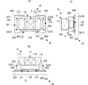
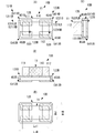
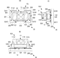
- FIG. 1 is a three-view diagram illustrating a configuration of an electronic component 10 including an interposer 12 according to a first embodiment, and a diagram illustrating a shape relationship between the interposer 12 and the multilayer ceramic capacitor 11.
- FIG. It is a trihedral view of the interposer 12 according to the first embodiment.
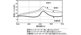
- FIG. 3 is a three-side view of the electronic component 10 according to the first embodiment mounted on a circuit board 20. It is a figure which shows the sound pressure level-frequency characteristic by the structure of 1st Embodiment, and the conventional structure.
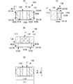
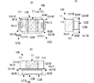
- FIG. 6 is a three-sided view in a state where an electronic component 10A according to a second embodiment is mounted on a circuit board 20; It is a figure which shows the three-plane figure which shows the structure of the electronic component 10B containing the interposer 12B which concerns on 3rd Embodiment, and the relationship of the shape of the interposer 12B and the multilayer ceramic capacitor 11.
- FIG. 6 is a three-sided view in a state where an electronic component 10A according to a second embodiment is mounted on a circuit board 20; It is a figure which shows the three-plane figure which shows the structure of the electronic component 10B containing the interposer 12B which concerns on 3rd Embodiment, and the relationship of the shape of the interposer 12B and the multilayer ceramic capacitor 11.
- FIG. 10 is a three-sided view illustrating a state in which an electronic component 10J according to another embodiment is mounted on a circuit board 200.
- FIG. 1 is a three-view diagram illustrating a configuration of an electronic component 10 including an interposer 12 according to the present embodiment, and a diagram illustrating a shape relationship between the interposer 12 and the multilayer ceramic capacitor 11.
- FIG. 2 is a three-side view of the interposer 12 according to this embodiment.
- FIG. 3 is a three-side view showing a state in which the electronic component 10 according to the present embodiment is mounted on the circuit board 200. 1, 2, and 3, each view (A) is a plan view, each view (B) is a length side view, and each view (C) is a width side view. Yes.
- the plan view is a view of the interposer 12 or the electronic component 10 as viewed from the upper surface side.
- the side view in the length direction shows that the interposer 12 or the electronic component 10 is orthogonal to the direction in which intermediate connection electrodes (hereinafter referred to as “IP electrodes”) 121 and 122 of the interposer 12 are arranged. It is the figure seen from the direction parallel to a surface (mounting surface of the multilayer ceramic capacitor 11).
- the side view in the width direction shows that the interposer 12 or the electronic component 10 is parallel to the direction in which the IP electrodes 121 and 122 of the interposer 12 are arranged, and is on the main surface of the interposer 12 (mounting surface of the multilayer ceramic capacitor 11).
- the multilayer ceramic capacitor 11 corresponds to a “chip component” of the present invention and includes a component main body 110.
- the component main body 110 is formed by laminating a predetermined number of dielectric layers and inner electrode layers and firing.
- the multilayer ceramic capacitor 11 has an external electrode 111 (corresponding to the “first external electrode” in the present invention) formed at one end in the length direction of the component main body 110 (the horizontal direction of the drawing shown in FIG. 1A).
- the external electrode 112 (corresponding to the “second external electrode” of the present invention) is formed at the opposite end.
- the external electrodes 111 and 112 are formed by firing a predetermined conductive paste, and the surface thereof is tin-plated.
- the direction in which the external electrodes 111 and 112 are arranged is defined as the length direction of the multilayer ceramic capacitor 11
- the direction perpendicular to the length direction and parallel to the mounting surface on which the multilayer ceramic capacitor 11 is mounted is defined as the multilayer ceramic capacitor. 11 will be described as the width direction.
- the external electrodes 111 and 112 are formed so as to spread not only from both end surfaces in the length direction of the component main body 110 but from both end surfaces in the length direction to both end surfaces in the width direction, the top surface, and the bottom surface.
- the multilayer ceramic capacitor 11 thus formed has, for example, a length ⁇ width of 3.2 mm ⁇ 1.6 mm, 2.0 mm ⁇ 1.25 mm, 1.6 mm ⁇ 0.8 mm, 1.0 mm ⁇ 0. It is formed with dimensions of 5 mm, 0.6 mm ⁇ 0.3 mm, and the like.
- the interposer 12 corresponds to a “substrate” of the present invention, and includes an insulating substrate 120 as shown in FIG.
- the insulating substrate 120 has a thickness of about 0.5 mm to 1.0 mm, for example, and is made of an insulating resin.
- the insulating substrate 120 is formed in a substantially rectangular shape similar to the multilayer ceramic capacitor 11 when viewed from the direction orthogonal to the main surface.
- the insulating substrate 120 has notches Cd11, Cd12, Cd13, and Cd14 formed in a shape in which four corners are recessed toward the center of the main surface when viewed from a direction orthogonal to the main surface.
- the notches Cd11, Cd12, Cd13, and Cd14 have a shape that is notched at a predetermined radius R around each corner of the rectangular insulating substrate 120 when viewed from the direction orthogonal to the main surface. Is formed.
- Such notches Cd11, Cd12, Cd13, and Cd14 are points where four adjacent insulating substrates 120 contact each other when the individual insulating substrates 120 are divided from the base substrate on which the plurality of insulating substrates 120 are arranged. It can be easily formed by forming a cylindrical through-hole and then cutting and dividing it so as to pass through the through-hole forming portion.
- the insulating substrate 120 is formed such that the length and width in plan view are slightly larger than the length and width of the multilayer ceramic capacitor 11 to be mounted. That is, as shown in FIG. 1D, when the length of the multilayer ceramic capacitor 11 is Lci and the length of the insulating substrate 120 (interposer 12) is Li, Li ⁇ Lci and Li> Lci. To do. Similarly, when the width of the multilayer ceramic capacitor 11 is Wci and the width of the insulating substrate 120 (interposer 12) is Wi, Wi ⁇ Wci and Wi> Wci.
- the central portion of the curved surface that defines the notches Cd11, Cd12, Cd13, and Cd14 is formed so as to fall within the outer shape range of the mounted multilayer ceramic capacitor 11.
- Upper surface electrodes 1211 and 1221 are formed on one main surface of the insulating substrate 120 on which the multilayer ceramic capacitor 11 is mounted.
- the upper surface electrodes 1211 and 1221 are formed apart from each other.
- the upper surface electrode 1211 corresponds to the “first upper surface electrode” of the present invention
- the upper surface electrode 1221 corresponds to the “second upper surface electrode” of the present invention.
- the upper surface electrode 1211 is formed in one end region in the length direction of the one main surface. At this time, when the multilayer ceramic capacitor 11 is mounted on one main surface of the interposer 12 (insulating substrate 120) so that the length directions of the top electrode 1211 substantially coincide with each other, The formation dimension of the electrode with respect to the length direction is set so as to include a region where the bottom surface of the external electrode 111 is in contact. The upper surface electrode 1211 is formed over the entire width in the width direction.
- the upper surface electrode 1221 is formed in the region of the other end in the length direction of the one main surface. At this time, when the multilayer ceramic capacitor 11 is mounted on the one main surface of the interposer 12 (insulating substrate 120) so that the length directions of the top electrode 1221 are substantially coincident with each other, The formation dimension of the electrode in the length direction is set so as to include a region where the bottom surface of the external electrode 112 is in contact. The upper surface electrode 1221 is formed over the entire width in the width direction.
- Lower surface electrodes 1212 and 1222 are formed on the other main surface of the insulating substrate 120 opposite to the side on which the multilayer ceramic capacitor 11 is mounted.
- the lower surface electrodes 1212 and 1222 are formed apart from each other.
- the lower electrode 1212 corresponds to the “first lower electrode” of the present invention
- the lower electrode 1222 corresponds to the “second lower electrode” of the present invention.
- the lower surface electrode 1212 is formed in a region of one end in the length direction of the other main surface of the insulating substrate 120 in a shape substantially opposite to the upper surface electrode 1211.
- the lower surface electrode 1222 is formed in a shape substantially opposite to the upper surface electrode 1221 in the region of the other end in the length direction of the other main surface of the insulating substrate 120.
- the lower surface electrodes 1212 and 1222 are formed so that the electrodes are present at positions overlapping the external electrodes 111 and 112 of the multilayer ceramic capacitor 11 to be mounted as viewed from the direction orthogonal to the main surface. More preferred.
- the upper surface electrode 1211 and the lower surface electrode 1212 formed at one end in the length direction of the insulating substrate 120 are connected to each other by connection electrodes 401 and 402 formed on the wall surfaces of the notches Cd11 and Cd12.
- the upper surface electrode 1211, the lower surface electrode 1212, the connection electrode 401 of the notch Cd11, and the connection electrode 402 of the notch Cd12 form the above-described IP electrode 121.
- the upper surface electrode 1221 and the lower surface electrode 1222 formed on the other end in the length direction of the insulating substrate 120 are connected to each other by connection electrodes 403 and 403 formed on the wall surfaces of the notches Cd13 and Cd14.
- the upper electrode 1221, the lower electrode 1222, the connection electrode 403 of the notch Cd13, and the connection electrode 404 of the notch Cd14 form the IP electrode 122 described above.
- the upper electrode 1211 of the IP electrode 121 of the interposer 12 and the external electrode 111 of the multilayer ceramic capacitor 11 are re-plated with tin plating of the external electrode 111. Electrically and mechanically connected by melting. Further, the upper electrode 1221 of the IP electrode 122 of the interposer 12 and the external electrode 112 of the multilayer ceramic capacitor 11 are electrically and mechanically connected by remelting tin plating of the external electrode 112. If tin plating is performed on the IP electrodes 121 and 122 in advance, the IP electrodes 121 and 122 are connected including the tin plating.
- the multilayer ceramic capacitor 11 and the interposer 12 may be joined with substantially the same amount of solder without using the tin plating of the external electrodes 111 and 112 or the tin plating of the interposer 12.
- the electronic component 10 is mounted on the circuit board 20 as shown in FIG. At this time, the mounting is performed so that the lower surface electrode 1212 of the IP electrode 121 of the interposer 12 is connected to the mounting land 201 of the circuit board 20 and the lower surface electrode 1222 of the IP electrode 122 of the interposer 12 is connected to the mounting land 202. Is done. Solder 300 is used to connect the IP electrodes 121 and 122 of the interposer 12 and the mounting lands 201 and 202 of the circuit board 20.
- solder joining is performed so that a solder fillet is formed at least from the mounting lands 201, 201 of the circuit board 20 to the connection electrodes 401-404 of the interposer 12.
- a solder fillet is formed at least from the mounting lands 201, 201 of the circuit board 20 to the connection electrodes 401-404 of the interposer 12.
- solder 300 a material other than the solder 300 may be used as long as the bonding agent has wettability and conductivity.
- solder fillet is formed by the connection electrodes 401-404 of the IP electrodes 121 and 122, and the connection via the connection electrodes 401-404.
- the solder 300 may rise up to the upper surface side of the positioner 12.
- connection electrodes 401-404 are formed only at the four corners of the interposer 12, and the notches Cd11, Cd12, Cd13, Cd14 in which the connection electrodes 401-404 are formed include the main electrodes. This coincides with the four corners of the multilayer ceramic capacitor 11 viewed from the direction orthogonal to the plane, that is, the positions of the four ridge lines extending in the direction orthogonal to the main surface of the external electrodes 111 and 112. With this configuration, as shown in FIG.
- the solder 300 extends from the lower ends of the four ridge lines of the external electrodes 111 and 112 corresponding to the notches Cd11, Cd12, Cd13, and Cd14 near the four corners to the four ridge lines. It adheres along. Thereby, the solder 300 does not adhere to the vicinity of the center of the end surfaces of the external electrodes 111 and 112, and generation of vibration noise due to the distortion of the multilayer ceramic capacitor 11 as described above can be effectively suppressed.
- FIG. 4 is a diagram showing sound pressure level-frequency characteristics according to the configuration of the present embodiment and the conventional configuration.
- the conventional configuration in FIG. 4 is a configuration in which a multilayer ceramic capacitor is directly mounted on a circuit board without using an interposer (mode T0), and a configuration in which the end surface center of the external electrode is soldered mainly over the entire end surface while using the interposer. (Aspect I0).
- the sound pressure level of the vibration sound can be significantly suppressed in a wide frequency band as compared with the conventional aspect T0.
- the sound pressure level of the vibration sound can be effectively suppressed as compared with the conventional mode I0.
- the interposer 12 made of the thin insulating substrate 120 as in the present embodiment, the height of the electronic component 10 can be suppressed and the height can be reduced.
- the multilayer ceramic capacitor 11 and the interposer 12 are stacked and mounted so that the main surfaces thereof coincide with the circuit board 20, high bonding strength can be realized. As a result, substantially the same bonding strength as when the multilayer ceramic capacitor 11 is directly mounted on the circuit board 20 can be obtained.
- the mounting lands 201 and 202 have the same specifications and the same intervals as those in the case where the multilayer ceramic capacitor 11 is directly mounted.
- the electronic component 10 of the present embodiment has the positions of the IP electrodes 121 and 122 of the interposer 12 and the positions of the external electrodes 111 and 112 of the multilayer ceramic capacitor 11 when viewed from the direction orthogonal to the main surface. Since the connection electrodes 401-404 are present at substantially the same position as the four ridge lines of the external electrodes 111, 112 of the multilayer ceramic capacitor 11, the mounting lands 201, 202 have the same specifications as when the multilayer ceramic capacitor 11 is directly mounted.
- the electronic component 10 can be mounted as it is. That is, it is not necessary to change the design of the mounting lands 201 and 202 of the circuit board 20.
- the electronic component 10 is mounted with substantially the same area as when the monolithic ceramic capacitor 11 is mounted on the circuit board 20. Thereby, even if the interposer 12 is used, the multilayer ceramic capacitor 11 can be connected to the circuit board 20 with almost no increase in size in plan view.
- FIG. 5A to 5C are three views showing the configuration of the electronic component 10A including the interposer 12A according to this embodiment.
- FIG. 5D is a diagram showing a shape relationship between the interposer 12 ⁇ / b> A and the multilayer ceramic capacitor 11.
- FIG. 6 is a three-side view of the electronic component 10 ⁇ / b> A according to this embodiment mounted on the circuit board 20.
- the basic configuration of the interposer 12A of the present embodiment is the same as that of the interposer 12 shown in the first embodiment, but the length and width are different.
- the length LiA of the interposer 12A, that is, the insulating substrate 120A is slightly shorter than the length Lci of the multilayer ceramic capacitor 11. That is, LiA ⁇ Lci and LiA ⁇ Lci.
- the width of the interposer 12A, that is, the insulating substrate 120A is substantially the same as the width of the multilayer ceramic capacitor 11 and is short. That is, WiA ⁇ Wci and WiA ⁇ Wci.
- solder 300 when solder joining to the circuit board 20 similar to that of the first embodiment is performed, when a large amount of solder is supplied, the solder 300 is notched portion Cd11A as shown in FIG. , Cd12A, Cd13A, and Cd14A (connection electrodes 401A, 402A, 403A, and 404A) are attached along the four ridge lines from the lower ends of the four ridge lines of the external electrodes 111 and 112, respectively. Thereby, the solder 300 does not adhere to the vicinity of the center of the end surfaces of the external electrodes 111 and 112, and generation of vibration noise due to the distortion of the multilayer ceramic capacitor 11 as described above can be effectively suppressed.
- the same mounting land as that used when mounting the monolithic ceramic capacitor 11 on the circuit board 20 can be used.
- the electronic component 10 can be mounted with the same area as when the multilayer ceramic capacitor 11 is mounted alone. Thereby, even if the interposer 12 is used, further downsizing is possible.
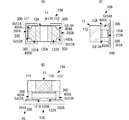
- FIGS. 7A to 7C are three views showing the configuration of the electronic component 10B including the interposer 12B according to the present embodiment.
- FIG. 7D is a diagram showing a shape relationship between the interposer 12 ⁇ / b> B and the multilayer ceramic capacitor 11.
- the interposer 12B of the present embodiment has a structure in which the length and width are larger than those of the interposer 12 shown in the first embodiment. Specifically, when the length of the interposer 12B is LiB and the width is WiB, LiB> Lci and WiB> Wci.
- the notches Cd11B, Cd12B, Cd13B, and Cd14B are formed so as to be linear when viewed from the direction orthogonal to the main surface.
- the notches Cd11B, Cd12B, Cd13B, and Cd14B are formed in a shape that does not enter the inside of the outer shape of the multilayer ceramic capacitor 11 when viewed from the direction orthogonal to the main surface.
- connection electrodes 401B, 402B, 403B, and 404B formed in the notches Cd11B, Cd12B, Cd13B, and Cd14B are connected to the external electrodes 111 and 112 of the multilayer ceramic capacitor 11 with respect to the external electrodes 111 and 112. It is closest to the end portion on the side of the interposer 12B of the four ridges extending in the direction orthogonal to the main surface of the electrodes 111, 112.
- connection electrodes 401B, 402B, 403B, and 404B adheres to the external electrodes 111 and 112
- the upper surface electrode 1211B of the IP electrode 121B of the interposer 12B is composed of partial upper surface electrodes 1211LB and 1211RB formed apart from each other in the width direction. That is, an electrode separation portion 500 (corresponding to “contact restricting means” of the present invention) sandwiched between the partial upper surface electrodes 1211LB and 1211RB is formed on the upper surface of the interposer 12B.
- These partial upper surface electrodes 1211LB and 1211RB are formed in a range including the positions of the two ridge lines of the external electrode 111.
- the upper surface electrode 1221B of the IP electrode 122B of the interposer 12B includes partial upper surface electrodes 1221LB and 1221RB that are formed apart from each other in the width direction. That is, an electrode separation portion 500 (corresponding to “contact restricting means” of the present invention) sandwiched between the partial upper surface electrodes 1221LB and 1221RB is formed on the upper surface of the interposer 12B.
- These partial upper surface electrodes 1221LB and 1221RB are formed within a range including the positions of the two ridge lines of the external electrode 112.
- the upper surface electrode is not formed near the center in the width direction (electrode separation portion 500) on the end surfaces of the external electrodes 111 and 112, and the width direction on the end surfaces of the external electrodes 111 and 112 is not formed. Solder adhesion near the center can be prevented. Thereby, generation
- the bottom electrodes of the IP electrodes 121B and 122B are not separated in the width direction, but may be separated.
- FIG. 8 is a three-side view showing the configuration of an electronic component 10C including the interposer 12C according to this embodiment.
- the interposer 12C of the present embodiment has an upper surface electrode formed over the entire width of the interposer 12C, and other configurations are the same as those of the interposer 12B shown in the third embodiment.
- the upper electrode 1211C of the IP electrode 121C of this embodiment is formed over the entire width of the interposer 12C.
- the upper surface electrode 1221C of the IP electrode 122C is also formed over the entire width of the interposer 12C.
- connection electrodes 401C, 402C, 403C, and 404C formed in the notches Cd11C, Cd12C, Cd13C, and Cd14C are not formed in the multilayer ceramic capacitor 11.
- the outer electrodes 111 and 112 are closest to the interposer 12C side end portion of the four ridges extending in the direction orthogonal to the main surface of the outer electrodes 111 and 112.
- the solder wets through the connection electrodes 401C, 402C, 403C, and 404C and adheres to the external electrodes 111 and 112, it adheres only to the vicinity of the four ridge lines of the external electrodes 111 and 112. Therefore, the generation of vibration noise can be suppressed as in the third embodiment.
- FIG. 9 is a trihedral view showing the configuration of an electronic component 10D including the interposer 12D according to the present embodiment.
- the interposer 12D of this embodiment is obtained by forming a solder resist film Re12 on the upper surface electrodes 1211D and 1221D, and the other configuration is the same as that of the interposer 12 shown in the first embodiment.
- the solder resist film Re12 corresponds to the “contact restricting means” of the present invention, and a perpendicular line extending from the center position in the width direction of the external electrodes 111 and 112 of the multilayer ceramic capacitor 11 to the upper surface electrodes 1211D and 1221D becomes the upper surface electrodes 1211D and 1221D. It is formed in a range of a predetermined width including a position that is orthogonal.
- the solder resist film Re12 is also formed in a predetermined length range including the position where the perpendicular is orthogonal to the upper surface electrodes 1211D and 1221D in the length direction of the interposer 12D. Accordingly, the vicinity of the center in the width direction of the external electrodes 111 and 112 is not in contact with the upper surface electrodes 1211D and 1221D of the IP electrodes 121D and 122D.
- FIG. 10 is a three-plane view showing the configuration of an electronic component 10E including the interposer 12E according to this embodiment.
- the illustration of the multilayer ceramic capacitor 11 is simplified in order to clearly show the structure of the interposer 12E.
- the interposer 12E of the present embodiment is different from the third embodiment in the formation positions of the notches Cd61 and Cd62, and the other configurations are the same as the interposer 12B shown in the third embodiment. The same.
- the upper surface electrode 1211E of the IP electrode 121E of the interposer 12E includes partial upper surface electrodes 1211LE and 1211RE that are spaced apart along the width direction of the interposer 12E, that is, the insulating substrate 120E. That is, an electrode separation portion 501 sandwiched between the partial upper surface electrodes 1211LE and 1211RE is formed on the upper surface of the interposer 12E. In the electrode separation portion 501, the upper surface of the insulating substrate 120E of the interposer 12E and the external electrode 111 of the multilayer ceramic capacitor 11 directly face each other.
- the partial upper surface electrodes 1211LE and 1211RE are connected by connection electrodes formed near one end in the length direction of the insulating substrate 120E and closer to the end than the position where the external electrode 111 of the multilayer ceramic capacitor 11 is placed. Has been.
- the notch Cd61 is an end surface of the insulating substrate 120E on the side where the IP electrode 121E is formed, and is formed at a substantially central position in the width direction of the insulating substrate 120E.
- the shape of the notch Cd61 is an arc shape when viewed from the direction orthogonal to the main surface, like the notches Cd11, Cd12, Cd13, and Cd14 shown in the first embodiment.
- a connection electrode 411E is formed on the wall surface of the notch Cd61, and is connected to the partial upper surface electrodes 1211LE and 1211RE via the electrodes connecting the partial upper surface electrodes 1211LE and 1211RE.
- the upper surface electrode 1221E of the IP electrode 122E of the interposer 12E includes partial upper surface electrodes 1221LE and 1221RE that are spaced apart along the width direction of the interposer 12E, that is, the insulating substrate 120E.
- an electrode separation portion 501 sandwiched between the partial upper surface electrodes 1221LE and 1221RE is formed on the upper surface of the interposer 12E.
- the upper surface of the insulating substrate 120E of the interposer 12E and the external electrode 112 of the multilayer ceramic capacitor 11 directly face each other.
- the partial upper surface electrodes 1221LE and 1221RE are connected by connection electrodes formed near the other end in the length direction of the insulating substrate 120E and on the end side from the position where the external electrode 112 of the multilayer ceramic capacitor 11 is placed. Has been.
- the notch Cd62 is an end surface of the insulating substrate 120E on the side where the IP electrode 122E is formed, and is formed at a substantially central position in the width direction of the insulating substrate 120E.
- the shape of the notch Cd62 is an arc shape when viewed from the direction orthogonal to the main surface.
- a connection electrode 412E is formed on the wall surface of the notch Cd62, and is connected to the partial upper surface electrodes 1221LE and 1221RE via the electrodes connecting the partial upper surface electrodes 1221LE and 1221RE.
- the top surface is provided as described in the above embodiments.
- the solder wetted on the electrodes 121E and 122E adheres to the vicinity of the four ridge lines of the external electrodes 111 and 112, and does not adhere to the vicinity of the center in the width direction.
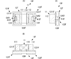
- FIG. 11 is a trihedral view showing the configuration of the electronic component 10F including the interposer 12F according to the present embodiment.
- the multilayer ceramic capacitor 11 is simplified in order to clearly show the structure of the interposer 12F.
- the interposer 12F is formed by forming upper surface electrodes 1211F and 1221F so as to cover substantially the entire width of the insulating substrate 120F with respect to the interposer 12E shown in the sixth embodiment.
- the formation parts 131F and 132F are provided, and the other configurations are the same.
- the electrode non-forming portion 131F is formed in a range of a predetermined width including a position where a perpendicular line extending from the center position in the width direction of the external electrode 111 of the multilayer ceramic capacitor 11 to the upper surface electrode 1211F is orthogonal to the upper surface electrode 1211F.
- the electrode non-forming portion 131F is formed in a predetermined length range including a position where the perpendicular is orthogonal to the upper surface electrode 1211F in the length direction of the interposer 12F, that is, the length direction of the insulating substrate 120F.
- an electrode opening pattern is formed near the center in the width direction of the external electrode 111 on the upper surface of the interposer 12F.
- the vicinity of the center in the width direction of the external electrode 111 is not in contact with the upper surface electrode 1211F of the IP electrode 121F.
- the electrode non-forming portion 132F is formed in a range of a predetermined width including a position where a perpendicular line extending from the center position in the width direction of the external electrode 112 of the multilayer ceramic capacitor 11 to the upper surface electrode 1221F is orthogonal to the upper surface electrode 1221F.
- the electrode non-forming portion 132F is formed in a range of a predetermined length including the position where the perpendicular is orthogonal to the upper surface electrode 1221F in the length direction of the interposer 12F, that is, the length direction of the insulating substrate 120F.
- an electrode opening pattern is formed near the center in the width direction of the external electrode 112 on the upper surface of the interposer 12F. Thereby, the vicinity of the center in the width direction of the external electrode 112 is not in contact with the upper surface electrode 1221F of the IP electrode 122F.
- FIG. 12 is a three-view diagram illustrating the configuration of an electronic component 10G including the interposer 12G according to the present embodiment.
- the multilayer ceramic capacitor 11 is simplified to clearly show the structure of the interposer 12G.
- the interposer 12G of the present embodiment is obtained by forming a solder resist film Re12G at the same position as the electrode non-forming portions 131F and 132F shown in the seventh embodiment, and other configurations are the seventh embodiment. Is the same. In this case, in FIG. 12, the upper surface electrode is illustrated as being formed at the position, but the upper surface electrode may or may not be formed at the position.
- This solder resist film Re12G corresponds to the “contact regulating means” of the present invention.
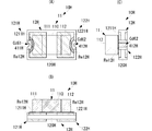
- FIG. 13 is a three-view diagram illustrating the configuration of an electronic component 10H including the interposer 12H according to the present embodiment.
- the multilayer ceramic capacitor 11 is simplified to clearly show the structure of the interposer 12H.
- the interposer 12H of this embodiment does not form the electrode non-forming portions 131F and 132F shown in the seventh embodiment, and the upper surface electrodes 1211H and 1221H are formed over substantially the entire width of the insulating substrate 120H.
- a solder resist film Re12H is formed on the upper surface electrodes 1211H and 1221H.
- Other configurations are the same as those of the seventh embodiment.
- the solder resist film Re12H is formed in a range of a predetermined width including a position where a perpendicular extending from the center position in the width direction of the external electrodes 111 and 112 of the multilayer ceramic capacitor 11 to the upper surface electrodes 1211H and 1221H is orthogonal to the upper surface electrodes 1211H and 1221H. ing.
- the solder resist film Re12H is also formed in a predetermined length range including the positions where the perpendiculars are orthogonal to the upper surface electrodes 1211H and 1221H with respect to the length direction of the interposer 12H. This solder resist film Re12H corresponds to the “contact regulating means” of the present invention.
- the solder resist film Re12H includes a region where the upper surface electrodes 1211H and 1221H are connected to the connection electrodes 411H and 412H of the notches Cd61 and Cd62, and a region where the upper surface electrodes 1211H and 1221H are in contact with the four ridge lines of the external electrodes 111 and 112.
- FIG. 14 is a three-view diagram illustrating the configuration of an electronic component 10K including the interposer 12K according to the present embodiment.
- the multilayer ceramic capacitor 11 is simplified to clearly show the structure of the interposer 12K.
- the interposer 12K of this embodiment is different from the interposer 12H shown in the ninth embodiment in the shape of the solder resist film Re12K, and the other configurations are the same.
- the solder resist film Re12K is perpendicular to the upper surface electrodes 1211K and 1221K with respect to the length direction of the interposer 12K.
- the perpendicular line extends from the center position in the width direction of the outer electrodes 111 and 112 of the multilayer ceramic capacitor 11 to the upper surface electrodes 1211K and 1221K. And a shape that reaches both ends in the length direction.
- This solder resist film Re12K corresponds to the “regulator” of the present invention.
- solder resist film Re12K is formed in such a shape as to cover the opening ends on the upper surface electrodes 1211K and 1221K side of the notches Cd61 and Cd62 including the connection electrodes 411K and 412K.
- the solder resist film Re12K can The wetting up to the upper surface side of the interposer 12K can be blocked. Thereby, it is possible to prevent the solder for mounting on the circuit board from unnecessarily adhering to the upper surface side of the interposer 12K, that is, the external electrodes 111 and 112 of the multilayer ceramic capacitor 11. As a result, the generation of vibration noise can be suppressed as in the above-described embodiments.
- FIG. 15 is a three-view diagram illustrating the configuration of an electronic component 10L including the interposer 12L according to the present embodiment.
- the multilayer ceramic capacitor 11 is simplified in order to clearly show the structure of the interposer 12L.
- the interposer 12L of the present embodiment is different from the interposer 12K shown in the tenth embodiment in the shape of the solder resist film Re12L, and the other configurations are the same.
- the solder resist film Re12L is formed so as to cover the upper surface electrodes 1211L and 1221L side of the notches Cd61 and Cd62 including the connection electrodes 411L and 412L of the interposer 12L.
- the solder resist film Re12L of the present embodiment has the end portion on the center side in the length direction up to a position where the external electrodes 111 and 112 of the multilayer ceramic capacitor 11 are in contact with (mounted on) the upper surface electrodes 1211L and 1221L. It is formed in a shape that does not reach. In other words, the solder resist film Re12L is formed in a shape as small as possible while minimizing covering the notches Cd61 and Cd62. This solder resist film Re12L corresponds to the “regulator” of the present invention.
- the interposer 12L of the present embodiment also has solder for mounting on the circuit board. It is possible to prevent unnecessary attachment to the upper surface side of the interposer 12L, that is, the external electrodes 111 and 112 of the multilayer ceramic capacitor 11. As a result, the generation of vibration noise can be suppressed as in the above-described embodiments.
- the solder resist film Re12L has a shape that does not extend to the region where the multilayer ceramic capacitor 11 is mounted. Therefore, when the multilayer ceramic capacitor 11 is mounted on the upper surface electrodes 1211L and 1221L, The solder resist film Re12L is not interposed between the bottom surfaces of the external electrodes 111 and 112 of the multilayer ceramic capacitor 11 and the top surface electrodes 1211L and 1221L. As a result, the bottom surfaces of the external electrodes 111 and 112 of the multilayer ceramic capacitor 11 and the top surface electrodes 1211L and 1221L are reliably in contact with each other without being separated. Therefore, the bonding strength between the bottom surfaces of the external electrodes 111 and 112 of the multilayer ceramic capacitor 11 and the top surface electrodes 1211L and 1221L is improved.
- solder resist film shown in the tenth embodiment and the eleventh embodiment is formed only in the center region in the width direction of the interposer, it may be formed over the entire region in the width direction.
- the interposers shown in the tenth embodiment and the eleventh embodiment have a notch formed at the center in the width direction. Even if the portion is provided, the solder resist film can be formed so as to cover the notch. As a result, as in the tenth and eleventh embodiments, unnecessary adhesion of solder to the external electrodes can be prevented.
- the solder resist film is used as an example.
- the metal film is formed so as to cover the notch from the upper surface electrode side. Any plate-like member can be used as long as it prevents the solder from getting wet.
- each of the above-described embodiments may be used independently, but the configuration of a plurality of embodiments may be used in combination. Furthermore, if the shape can be inferred based on the configuration of these embodiments, the same effects as those of the above-described embodiments can be obtained.
- an electrode non-forming portion or a resist film on the insulating substrate, it is possible to suppress the solder from attaching to the center of the end surface of the external electrodes 111 and 112 of the multilayer ceramic capacitor 11.
- Such an electrode non-formation portion or a resist film can be formed on the external electrodes 111 and 112.
- FIG. 16 is a three-sided view illustrating a state in which the electronic component 10J according to another embodiment is mounted on the circuit board 200.
- the electronic component 10J shown in FIG. 16 is different from the electronic component 10 shown in the first embodiment in the external electrodes of the multilayer ceramic capacitor 11J, and the other configurations are the same.
- the external electrodes 111J and 112J of the multilayer ceramic capacitor 11J of the electronic component 10J have a predetermined area at the end surface in the longitudinal direction of the component body 110, that is, at the center of the formation surface of the external electrodes 111J and 112J.
- the electrode non-forming part 140 is provided. By adopting such a configuration, it is possible to more reliably prevent solder from attaching to the center of the end surface where the external electrodes 111J and 112J of the component main body 110 are formed.
- the electrode non-forming portion 140 corresponds to the “joining restriction unit” of the present invention.
- FIG. 16 shows an example in which the electrode non-forming portion 140 is provided, but a resist film may be formed in the region regardless of the presence or absence of the electrode. Furthermore, the structure which forms an external electrode only in a bottom face may be sufficient. Such a configuration similar to FIG. 16 can be combined with the configuration of any of the above-described embodiments.
- the substantially rectangular shape shown in the present invention is not limited to a rectangular shape, but a square, a polygon obtained by cutting off the corners (corners) of these rectangles and squares, and the corners (corners) of the rectangles and squares are curved. Also includes shapes molded into
Landscapes
- Engineering & Computer Science (AREA)
- Power Engineering (AREA)
- Microelectronics & Electronic Packaging (AREA)
- Manufacturing & Machinery (AREA)
- Chemical & Material Sciences (AREA)
- Ceramic Engineering (AREA)
- Inorganic Chemistry (AREA)
- Structures For Mounting Electric Components On Printed Circuit Boards (AREA)
- Ceramic Capacitors (AREA)
- Fixed Capacitors And Capacitor Manufacturing Machines (AREA)
Abstract
Description
11,11J:積層セラミックコンデンサ、
110:部品本体、
111,112,111J,112J:外部電極、
12,12A,12B,12C,12D,12E,12F,12G,12H,12K,12L:インターポーザー、
120,120A,120B,120C,120D,120E,120E,120G,120H,120K,120L:絶縁性基板、
121,122,121A,122A,121B,122B,121C,122C,121D,122D,121E,122E,121F,122F,121G,122G,121H,122H,121K,122K,121L,122L:IP電極、
1211,1221,1211A,1221A,1211B,1221B,1211C,1221C,1211D,1221D,1211E,1221E,1211F,1221F,1211G,1221G,1211H,1221H,1211K,1221K,1211L,1221L:上面電極、
1211LB,1211RB,1221LB,1221RB,1211LE,1211RE,1221LE,1221RE:部分上面電極、
1212,1222:下面電極、
131F,132F:電極非形成部、
140:電極非形成部(外部電極)、
Cd11,Cd12,Cd13,Cd14,Cd11A,Cd12A,Cd13A,Cd14A,Cd11B,Cd12B,Cd13B,Cd14B,Cd11C,Cd12C,Cd13C,Cd14C,Cd11D,Cd12D,Cd13D,Cd14D,Cd61,Cd62:切り欠き部、
Re12,Re12G,Re12H,Re12K,Re12L:はんだレジスト膜、
20:回路基板、
201,202:実装用ランド、
401,402,403,404,401A,402A,403A,404A,401B,402B,403B,404B,401C,402C,403C,404C,401D,402D,403D,404D,411E,412E,411F,412F,411G,412G,411H,412H,411K,412K,411L,412L:接続電極、
500,501:電極離間部
Claims (18)
- 平板状の絶縁性基板、該絶縁性基板の一方主面に形成された第1上面電極、第2上面電極、前記絶縁性基板の他方主面に形成された第1下面電極、第2下面電極を備える基板と、
本体の長さ方向の両端にそれぞれ対向して第1外部電極と第2外部電極とが形成され、前記第1外部電極が前記第1上面電極に実装され、前記第2外部電極が前記第2上面電極に実装されるチップ部品と、を備える電子部品であって、
前記基板は、前記一方主面と前記他方主面に直交する端面に形成され、前記第1上面電極と前記第1下面電極を接続し、前記第2上面電極と前記第2上面電極とを接続する複数の接続電極を備え、
前記チップ部品の本体の長さ方向と直交する幅方向の略中央において、前記第1上面電極と前記第1下面電極とが離間し、前記第2上面電極と前記第2下面電極とが離間していることを特徴とする電子部品。 - 請求項1に記載の電子部品であって、
前記絶縁性基板には、前記チップ部品の前記第1外部電極に対応する位置に、それぞれ前記第1上面電極および前記第1下面電極が設けられ、前記チップ部品の前記第2外部電極に対応する位置に、それぞれ前記第2上面電極および前記第2下面電極が設けられ、
前記複数の接続電極は、前記絶縁性基板の四隅に形成されている、電子部品。 - 請求項2に記載の電子部品であって、
前記絶縁性基板の四隅には切り欠き部が形成されており、
該切り欠き部の内壁面に前記接続電極が形成されている、電子部品。 - 請求項3に記載の電子部品であって、
前記絶縁性基板に前記チップ部品を搭載した際に、前記一方主面および前記他方主面に直交する方向から見て、前記切り欠き部の少なくとも一部は前記チップ部品の外形で構成される領域内に存在する、電子部品。 - 請求項3または請求項4に記載の電子部品であって、
前記切り欠き部は、前記一方主面および前記他方主面に直交する方向から見た状態で、前記絶縁性基板の中心側に膨らむ円弧形状で形成されている、電子部品。 - 請求項3または請求項4に記載の電子部品であって、
前記絶縁性基板は、前記チップ部品を搭載した際、前記一方主面および前記他方主面に直交する方向から見た状態で、前記チップ部品の外形よりも小さい外形形状で形成されている、電子部品。 - 請求項1乃至請求項6のいずれかに記載の電子部品であって、
前記絶縁性基板は、前記チップ部品の前記第1外部電極および前記第2外部電極が形成される端部の中心から前記絶縁性基板に下ろした垂線が該絶縁性基板と交差する位置を含む所定範囲において、前記第1外部電極および前記第2外部電極に対して直接対面している、電子部品。 - 請求項1乃至請求項6のいずれかに記載の電子部品であって、
前記第1上面電極および前記第2上面電極の前記チップ部品を搭載する面には、前記チップ部品の前記第1外部電極および前記第2外部電極が形成される端部の中心から前記第1上面電極および前記第2上面電極に下ろした垂線が前記基板と交差する位置を含む所定範囲にレジスト膜が設けられている、電子部品。 - 平板状の絶縁性基板、該絶縁性基板の一方主面に形成された第1上面電極、第2上面電極、前記絶縁性基板の他方主面に形成された第1下面電極、第2下面電極を備える基板と、
本体の長さ方向の両端にそれぞれ対向して第1外部電極と第2外部電極とが形成され、前記第1外部電極が前記第1上面電極に実装され、前記第2外部電極が前記第2上面電極に実装されるチップ部品と、を備える電子部品であって、
前記基板は、前記一方主面と前記他方主面に直交する端面に形成され、前記第1上面電極と前記第1下面電極を接続し、前記第2上面電極と前記第2上面電極とを接続する複数の接続電極を備え、
前記第1上面電極および前記第2上面電極には、前記第1外部電極および前記第2外部電極の端面の中心から前記第1上面電極および前記第2上面電極に下ろした垂線が前記基板と交差する位置を含む所定範囲が前記第1上面電極および前記第2上面電極に対して非接触となる接触規制手段が形成されている、電子部品。 - 請求項9に記載の電子部品であって、
前記絶縁性基板には、前記チップ部品の前記第1外部電極に対応する位置に、それぞれ前記第1上面電極および前記第1下面電極が設けられ、前記チップ部品の前記第2外部電極に対応する位置に、それぞれ前記第2上面電極および前記第2下面電極が設けられ、
前記接触規制手段は、前記第1上面電極および前記第2上面電極に設けられた開口領域である、電子部品。 - 請求項9に記載の電子部品であって、
前記絶縁性基板には、前記チップ部品の前記第1外部電極に対応する位置に、それぞれ前記第1上面電極および前記第1下面電極が設けられ、前記チップ部品の前記第2外部電極に対応する位置に、それぞれ前記第2上面電極および前記第2下面電極が設けられ、
前記接触規制手段は、前記第1上面電極および前記第2上面電極に形成されたレジスト膜である、電子部品。 - 請求項9乃至請求項11のいずれかに記載の電子部品であって、
前記接続電極は、前記チップ部品の本体の長さ方向と直交する幅方向の略中央に形成されている、電子部品。 - 請求項9乃至請求項12のいずれかに記載の電子部品であって、
前記接続電極は、前記絶縁性基板の端面部に形成された切り欠き部の内壁面に形成されている、電子部品。 - 請求項13に記載の電子部品であって、
前記切り欠き部は、前記一方主面、前記他方主面に直交する方向から見た状態で、前記絶縁性基板の中心側に膨らむ円弧形状で形成されている、電子部品。 - 平板状の絶縁性基板、該絶縁性基板の一方主面に形成された第1上面電極、第2上面電極、前記絶縁性基板の他方主面に形成された第1下面電極、第2下面電極を備える基板と、
本体の長さ方向の両端にそれぞれ対向して第1外部電極と第2外部電極とが形成され、前記第1外部電極が前記第1上面電極に実装され、前記第2外部電極が前記第2上面電極に実装されるチップ部品と、を備える電子部品であって、
前記基板は、前記一方主面と前記他方主面に直交する端面に形成され、前記第1上面電極と前記第1下面電極を接続し、前記第2上面電極と前記第2上面電極とを接続する複数の接続電極を備え、
前記接続電極は、前記絶縁性基板の前記端面から凹む形状で形成された切り欠き部を形成する内壁面に形成されており、
該切り欠き部の前記第1上面電極側および前記第2上面電極側には、前記絶縁性基板を平面視して前記切り欠き部を覆う規制部が形成されている、電子部品。 - 請求項1乃至請求項15に記載の電子部品であって、
前記チップ部品の前記第1外部電極および前記第2外部電極が形成される端面の中心を含む所定範囲に接合規制手段が形成されている、電子部品。 - 請求項16に記載のチップ構造体であって、
前記接合規制手段は、前記端面の全面に亘る、チップ構造体。 - 請求項1乃至請求項17のいずれかに記載の電子部品であって、
前記チップ部品が、二端子型の積層セラミックコンデンサである、電子部品。
Priority Applications (5)
| Application Number | Priority Date | Filing Date | Title |
|---|---|---|---|
| JP2012550961A JP5376069B2 (ja) | 2010-12-28 | 2011-12-27 | 電子部品 |
| KR1020137016378A KR101485117B1 (ko) | 2010-12-28 | 2011-12-27 | 전자부품 |
| CN201180063327.8A CN103299382B (zh) | 2010-12-28 | 2011-12-27 | 电子部件 |
| KR1020147020944A KR101476391B1 (ko) | 2010-12-28 | 2011-12-27 | 전자부품 |
| US13/927,251 US9241408B2 (en) | 2010-12-28 | 2013-06-26 | Electronic component |
Applications Claiming Priority (4)
| Application Number | Priority Date | Filing Date | Title |
|---|---|---|---|
| JP2010-291413 | 2010-12-28 | ||
| JP2010291413 | 2010-12-28 | ||
| JP2011-121174 | 2011-05-31 | ||
| JP2011121174 | 2011-05-31 |
Related Child Applications (1)
| Application Number | Title | Priority Date | Filing Date |
|---|---|---|---|
| US13/927,251 Continuation US9241408B2 (en) | 2010-12-28 | 2013-06-26 | Electronic component |
Publications (1)
| Publication Number | Publication Date |
|---|---|
| WO2012090986A1 true WO2012090986A1 (ja) | 2012-07-05 |
Family
ID=46383080
Family Applications (1)
| Application Number | Title | Priority Date | Filing Date |
|---|---|---|---|
| PCT/JP2011/080164 Ceased WO2012090986A1 (ja) | 2010-12-28 | 2011-12-27 | 電子部品 |
Country Status (4)
| Country | Link |
|---|---|
| JP (2) | JP5376069B2 (ja) |
| KR (2) | KR101485117B1 (ja) |
| CN (2) | CN103299382B (ja) |
| WO (1) | WO2012090986A1 (ja) |
Cited By (21)
| Publication number | Priority date | Publication date | Assignee | Title |
|---|---|---|---|---|
| WO2013187186A1 (ja) * | 2012-06-14 | 2013-12-19 | 株式会社 村田製作所 | 電子部品及びその製造方法 |
| JP2013258240A (ja) * | 2012-06-12 | 2013-12-26 | Murata Mfg Co Ltd | チップ部品構造体 |
| JP2014057046A (ja) * | 2012-08-10 | 2014-03-27 | Murata Mfg Co Ltd | 実装ランド構造体及び積層コンデンサの実装構造体 |
| CN104064355A (zh) * | 2013-03-19 | 2014-09-24 | 株式会社村田制作所 | 电子部件以及电子部件串 |
| JP2015023245A (ja) * | 2013-07-23 | 2015-02-02 | 株式会社村田製作所 | 電子部品の製造方法 |
| JP2015023246A (ja) * | 2013-07-23 | 2015-02-02 | 株式会社村田製作所 | 電子部品の製造方法及び基板型の端子の製造方法 |
| JP2015095646A (ja) * | 2013-11-14 | 2015-05-18 | サムソン エレクトロ−メカニックス カンパニーリミテッド. | 積層セラミック電子部品及び積層セラミック電子部品の実装基板 |
| JP2015095647A (ja) * | 2013-11-14 | 2015-05-18 | サムソン エレクトロ−メカニックス カンパニーリミテッド. | 積層セラミック電子部品及び積層セラミック電子部品の実装基板 |
| JP2015185651A (ja) * | 2014-03-24 | 2015-10-22 | 株式会社村田製作所 | 電子部品 |
| JP2016072603A (ja) * | 2014-09-26 | 2016-05-09 | 株式会社村田製作所 | 電子部品 |
| JP2016086066A (ja) * | 2014-10-24 | 2016-05-19 | 株式会社村田製作所 | 電子部品、回路モジュール及び回路基板 |
| US9484152B2 (en) | 2013-03-15 | 2016-11-01 | Murata Manufacturing Co., Ltd. | Electronic component, substrate-type terminal included therein, and electronic component mounted structure |
| US9997295B2 (en) | 2014-09-26 | 2018-06-12 | Murata Manufacturing Co., Ltd. | Electronic component |
| US10014111B2 (en) | 2014-03-24 | 2018-07-03 | Murata Manufacturing Co., Ltd. | Substrate terminal mounted electronic element |
| US10128050B1 (en) | 2017-09-27 | 2018-11-13 | Samsung Electro-Mechanics Co., Ltd. | Composite electronic component and board having the same |
| CN109524238A (zh) * | 2017-09-20 | 2019-03-26 | 三星电机株式会社 | 多层电子组件及具有该多层电子组件的板 |
| JP2020047908A (ja) * | 2018-09-14 | 2020-03-26 | サムソン エレクトロ−メカニックス カンパニーリミテッド. | 電子部品 |
| US10699846B2 (en) | 2017-08-28 | 2020-06-30 | Samsung Electro-Mechanics Co., Ltd. | Composite electronic component and board having the same |
| CN113303033A (zh) * | 2019-01-28 | 2021-08-24 | 三菱电机株式会社 | 基板组件以及空气调和装置 |
| US20220108844A1 (en) * | 2020-10-07 | 2022-04-07 | Murata Manufacturing Co., Ltd. | Multilayer ceramic capacitor |
| US11495412B2 (en) * | 2020-04-23 | 2022-11-08 | Murata Manufacturing Co., Ltd. | Multilayer ceramic capacitor |
Families Citing this family (22)
| Publication number | Priority date | Publication date | Assignee | Title |
|---|---|---|---|---|
| JP5532087B2 (ja) * | 2012-08-06 | 2014-06-25 | 株式会社村田製作所 | 実装構造 |
| JP6014581B2 (ja) * | 2013-02-18 | 2016-10-25 | 太陽誘電株式会社 | インターポーザ付き積層セラミックコンデンサと、積層セラミックコンデンサ用インターポーザ |
| KR101525689B1 (ko) * | 2013-11-05 | 2015-06-03 | 삼성전기주식회사 | 적층 세라믹 전자 부품 및 적층 세라믹 전자 부품의 실장 기판 |
| JP6248644B2 (ja) * | 2014-01-17 | 2017-12-20 | Tdk株式会社 | 電子部品 |
| KR20150089277A (ko) * | 2014-01-27 | 2015-08-05 | 삼성전기주식회사 | 적층 세라믹 전자 부품 및 그 실장 기판 |
| KR101963273B1 (ko) * | 2014-09-18 | 2019-03-28 | 삼성전기주식회사 | 인터포저, 인터포저를 포함하는 전자 부품 및 인터포저를 포함하는 전자 부품의 실장 기판 |
| KR102139763B1 (ko) * | 2015-01-08 | 2020-07-31 | 삼성전기주식회사 | 적층 세라믹 전자 부품 및 그 실장 기판 |
| KR102214642B1 (ko) * | 2015-01-20 | 2021-02-10 | 삼성전기주식회사 | 적층 세라믹 전자 부품 및 그 실장 기판 |
| JP2017005221A (ja) * | 2015-06-16 | 2017-01-05 | 株式会社村田製作所 | 複合電子部品 |
| KR102516765B1 (ko) * | 2017-09-27 | 2023-03-31 | 삼성전기주식회사 | 적층형 전자 부품 및 그 실장 기판 |
| KR102426211B1 (ko) * | 2017-10-02 | 2022-07-28 | 삼성전기주식회사 | 적층형 전자 부품 및 그 실장 기판 |
| KR102473414B1 (ko) | 2017-10-12 | 2022-12-02 | 삼성전기주식회사 | 적층형 전자 부품 및 그 실장 기판 |
| US10892212B2 (en) | 2017-11-09 | 2021-01-12 | Stmicroelectronics, Inc. | Flat no-lead package with surface mounted structure |
| CN108257878A (zh) * | 2018-01-11 | 2018-07-06 | 郑州云海信息技术有限公司 | 一种增强qfn封装焊接效果的方法及qfn封装 |
| KR102609148B1 (ko) * | 2018-02-13 | 2023-12-05 | 삼성전기주식회사 | 전자 부품 및 그 실장 기판 |
| KR102505433B1 (ko) | 2018-04-20 | 2023-03-03 | 삼성전기주식회사 | 전자 부품 |
| KR102538898B1 (ko) * | 2018-06-08 | 2023-06-01 | 삼성전기주식회사 | 전자 부품 |
| CN108831871A (zh) * | 2018-06-08 | 2018-11-16 | 郑州云海信息技术有限公司 | 一种提升qfn封装零件焊接质量的设计方法 |
| KR20190121179A (ko) | 2018-09-13 | 2019-10-25 | 삼성전기주식회사 | 전자 부품 |
| KR102584973B1 (ko) | 2018-09-28 | 2023-10-05 | 삼성전기주식회사 | 복합 전자부품 |
| KR102109639B1 (ko) * | 2019-06-07 | 2020-05-12 | 삼성전기주식회사 | 적층 세라믹 전자 부품 및 그 실장 기판 |
| KR102283080B1 (ko) | 2019-12-30 | 2021-07-30 | 삼성전기주식회사 | 전자 부품 |
Citations (5)
| Publication number | Priority date | Publication date | Assignee | Title |
|---|---|---|---|---|
| JP2004134430A (ja) * | 2002-10-08 | 2004-04-30 | Tdk Corp | 電子部品 |
| JP2004335657A (ja) * | 2003-05-06 | 2004-11-25 | Tdk Corp | 底面電極チップ部品の表面実装用ランドパターン、表面実装方法、緩衝基板及び電子部品 |
| WO2005072033A1 (ja) * | 2004-01-27 | 2005-08-04 | Matsushita Electric Industrial Co., Ltd. | 回路基板およびチップ部品実装方法 |
| WO2009028463A1 (ja) * | 2007-08-24 | 2009-03-05 | Nec Corporation | スペーサ及びその製造方法 |
| WO2010134335A1 (ja) * | 2009-05-19 | 2010-11-25 | ルビコン株式会社 | 表面実装用のデバイスおよびコンデンサー素子 |
Family Cites Families (18)
| Publication number | Priority date | Publication date | Assignee | Title |
|---|---|---|---|---|
| JPS62184727U (ja) * | 1986-05-15 | 1987-11-24 | ||
| JPS62186462U (ja) * | 1986-05-20 | 1987-11-27 | ||
| JPS63187320U (ja) * | 1987-05-22 | 1988-11-30 | ||
| JPH01155668U (ja) * | 1988-04-19 | 1989-10-25 | ||
| JPH0677631A (ja) * | 1992-08-28 | 1994-03-18 | Matsushita Electric Ind Co Ltd | チップ部品のアルミ基板への実装方法 |
| JPH06132763A (ja) * | 1992-10-20 | 1994-05-13 | Rohm Co Ltd | 圧電発振子 |
| JPH06151231A (ja) * | 1992-10-29 | 1994-05-31 | Toshiba Lighting & Technol Corp | 電気部品 |
| JP3070364B2 (ja) * | 1992-11-25 | 2000-07-31 | 松下電器産業株式会社 | セラミック電子部品の製造方法 |
| JP2716342B2 (ja) * | 1993-06-28 | 1998-02-18 | 日本電気株式会社 | チップ型積層セラミックコンデンサ |
| JPH07111380A (ja) * | 1993-10-14 | 1995-04-25 | Murata Mfg Co Ltd | 表面実装用電子部品 |
| JPH08222478A (ja) * | 1995-02-16 | 1996-08-30 | Murata Mfg Co Ltd | チップ型電子部品 |
| JP3061031B2 (ja) * | 1998-04-17 | 2000-07-10 | 日立エーアイシー株式会社 | プリント配線基板 |
| JP2000012367A (ja) * | 1998-06-19 | 2000-01-14 | Sony Corp | 電子チップ部品およびその製造方法 |
| JP2000323959A (ja) * | 1999-05-14 | 2000-11-24 | Murata Mfg Co Ltd | 圧電部品 |
| US7307829B1 (en) * | 2002-05-17 | 2007-12-11 | Daniel Devoe | Integrated broadband ceramic capacitor array |
| JP2005130341A (ja) | 2003-10-27 | 2005-05-19 | Murata Mfg Co Ltd | 圧電部品及びその製造方法、通信装置 |
| JP4562516B2 (ja) * | 2004-12-24 | 2010-10-13 | 京セラ株式会社 | 電子部品収納用パッケージおよび電子装置 |
| JP2006186167A (ja) * | 2004-12-28 | 2006-07-13 | Tdk Corp | 電子部品 |
-
2011
- 2011-12-27 KR KR1020137016378A patent/KR101485117B1/ko active Active
- 2011-12-27 CN CN201180063327.8A patent/CN103299382B/zh active Active
- 2011-12-27 WO PCT/JP2011/080164 patent/WO2012090986A1/ja not_active Ceased
- 2011-12-27 CN CN201710319375.8A patent/CN107240496B/zh active Active
- 2011-12-27 KR KR1020147020944A patent/KR101476391B1/ko active Active
- 2011-12-27 JP JP2012550961A patent/JP5376069B2/ja active Active
-
2013
- 2013-09-18 JP JP2013192842A patent/JP5725112B2/ja active Active
Patent Citations (5)
| Publication number | Priority date | Publication date | Assignee | Title |
|---|---|---|---|---|
| JP2004134430A (ja) * | 2002-10-08 | 2004-04-30 | Tdk Corp | 電子部品 |
| JP2004335657A (ja) * | 2003-05-06 | 2004-11-25 | Tdk Corp | 底面電極チップ部品の表面実装用ランドパターン、表面実装方法、緩衝基板及び電子部品 |
| WO2005072033A1 (ja) * | 2004-01-27 | 2005-08-04 | Matsushita Electric Industrial Co., Ltd. | 回路基板およびチップ部品実装方法 |
| WO2009028463A1 (ja) * | 2007-08-24 | 2009-03-05 | Nec Corporation | スペーサ及びその製造方法 |
| WO2010134335A1 (ja) * | 2009-05-19 | 2010-11-25 | ルビコン株式会社 | 表面実装用のデバイスおよびコンデンサー素子 |
Cited By (38)
| Publication number | Priority date | Publication date | Assignee | Title |
|---|---|---|---|---|
| JP2013258240A (ja) * | 2012-06-12 | 2013-12-26 | Murata Mfg Co Ltd | チップ部品構造体 |
| US9978515B2 (en) | 2012-06-14 | 2018-05-22 | Murata Manufacturing Co., Ltd. | Electronic component unit and manufacturing method therefor |
| WO2013187186A1 (ja) * | 2012-06-14 | 2013-12-19 | 株式会社 村田製作所 | 電子部品及びその製造方法 |
| JP5664827B2 (ja) * | 2012-06-14 | 2015-02-04 | 株式会社村田製作所 | 電子部品及びその製造方法 |
| JP2014057046A (ja) * | 2012-08-10 | 2014-03-27 | Murata Mfg Co Ltd | 実装ランド構造体及び積層コンデンサの実装構造体 |
| US9484152B2 (en) | 2013-03-15 | 2016-11-01 | Murata Manufacturing Co., Ltd. | Electronic component, substrate-type terminal included therein, and electronic component mounted structure |
| CN104064355A (zh) * | 2013-03-19 | 2014-09-24 | 株式会社村田制作所 | 电子部件以及电子部件串 |
| JP2014207422A (ja) * | 2013-03-19 | 2014-10-30 | 株式会社村田製作所 | 電子部品および電子部品連 |
| US9313892B2 (en) | 2013-03-19 | 2016-04-12 | Murata Manufacturing Co., Ltd. | Electronic component and electronic component package |
| JP2015023246A (ja) * | 2013-07-23 | 2015-02-02 | 株式会社村田製作所 | 電子部品の製造方法及び基板型の端子の製造方法 |
| CN104347279A (zh) * | 2013-07-23 | 2015-02-11 | 株式会社村田制作所 | 电子部件的制造方法 |
| US9839135B2 (en) | 2013-07-23 | 2017-12-05 | Murata Manufacturing Co., Ltd. | Method of producing electronic components and method of producing substrate-type terminals |
| US9801283B2 (en) | 2013-07-23 | 2017-10-24 | Murata Manufacturing Co., Ltd. | Method of producing electronic components |
| CN104347267A (zh) * | 2013-07-23 | 2015-02-11 | 株式会社村田制作所 | 电子部件的制造方法以及基板型端子的制造方法 |
| JP2015023245A (ja) * | 2013-07-23 | 2015-02-02 | 株式会社村田製作所 | 電子部品の製造方法 |
| US9545005B2 (en) | 2013-11-14 | 2017-01-10 | Samsung Electro-Mechanics Co., Ltd. | Multilayer ceramic electronic component and board having the same mounted thereon |
| US9526174B2 (en) | 2013-11-14 | 2016-12-20 | Samsung Electro-Mechanics Co., Ltd. | Multilayer ceramic electronic component and board having the same mounted thereon |
| JP2015095647A (ja) * | 2013-11-14 | 2015-05-18 | サムソン エレクトロ−メカニックス カンパニーリミテッド. | 積層セラミック電子部品及び積層セラミック電子部品の実装基板 |
| JP2015095646A (ja) * | 2013-11-14 | 2015-05-18 | サムソン エレクトロ−メカニックス カンパニーリミテッド. | 積層セラミック電子部品及び積層セラミック電子部品の実装基板 |
| JP2015185651A (ja) * | 2014-03-24 | 2015-10-22 | 株式会社村田製作所 | 電子部品 |
| US9947466B2 (en) | 2014-03-24 | 2018-04-17 | Murata Manufacturing Co., Ltd. | Electronic component |
| US10014111B2 (en) | 2014-03-24 | 2018-07-03 | Murata Manufacturing Co., Ltd. | Substrate terminal mounted electronic element |
| JP2016072603A (ja) * | 2014-09-26 | 2016-05-09 | 株式会社村田製作所 | 電子部品 |
| US9997295B2 (en) | 2014-09-26 | 2018-06-12 | Murata Manufacturing Co., Ltd. | Electronic component |
| JP2016086066A (ja) * | 2014-10-24 | 2016-05-19 | 株式会社村田製作所 | 電子部品、回路モジュール及び回路基板 |
| US10699846B2 (en) | 2017-08-28 | 2020-06-30 | Samsung Electro-Mechanics Co., Ltd. | Composite electronic component and board having the same |
| CN109524238A (zh) * | 2017-09-20 | 2019-03-26 | 三星电机株式会社 | 多层电子组件及具有该多层电子组件的板 |
| US10453616B2 (en) | 2017-09-27 | 2019-10-22 | Samsung Electro-Mechanics Co., Ltd. | Composite electronic component and board having the same |
| US10614960B2 (en) | 2017-09-27 | 2020-04-07 | Samsung Electro-Mechanics Co., Ltd. | Composite electronic component and board having the same |
| US10128050B1 (en) | 2017-09-27 | 2018-11-13 | Samsung Electro-Mechanics Co., Ltd. | Composite electronic component and board having the same |
| JP2020047908A (ja) * | 2018-09-14 | 2020-03-26 | サムソン エレクトロ−メカニックス カンパニーリミテッド. | 電子部品 |
| CN114496567A (zh) * | 2018-09-14 | 2022-05-13 | 三星电机株式会社 | 电子组件 |
| JP7286952B2 (ja) | 2018-09-14 | 2023-06-06 | サムソン エレクトロ-メカニックス カンパニーリミテッド. | 電子部品 |
| CN113303033A (zh) * | 2019-01-28 | 2021-08-24 | 三菱电机株式会社 | 基板组件以及空气调和装置 |
| CN113303033B (zh) * | 2019-01-28 | 2024-02-13 | 三菱电机株式会社 | 基板组件以及空气调和装置 |
| US11495412B2 (en) * | 2020-04-23 | 2022-11-08 | Murata Manufacturing Co., Ltd. | Multilayer ceramic capacitor |
| US20220108844A1 (en) * | 2020-10-07 | 2022-04-07 | Murata Manufacturing Co., Ltd. | Multilayer ceramic capacitor |
| US11749461B2 (en) * | 2020-10-07 | 2023-09-05 | Murata Manufacturing Co., Ltd. | Multilayer ceramic capacitor |
Also Published As
| Publication number | Publication date |
|---|---|
| KR20140107622A (ko) | 2014-09-04 |
| JPWO2012090986A1 (ja) | 2014-06-05 |
| CN107240496A (zh) | 2017-10-10 |
| CN103299382B (zh) | 2017-05-24 |
| JP2014042037A (ja) | 2014-03-06 |
| KR101476391B1 (ko) | 2014-12-24 |
| JP5376069B2 (ja) | 2013-12-25 |
| KR101485117B1 (ko) | 2015-01-21 |
| KR20130115314A (ko) | 2013-10-21 |
| CN107240496B (zh) | 2019-06-07 |
| JP5725112B2 (ja) | 2015-05-27 |
| CN103299382A (zh) | 2013-09-11 |
Similar Documents
| Publication | Publication Date | Title |
|---|---|---|
| JP5376069B2 (ja) | 電子部品 | |
| US9552923B2 (en) | Electronic component | |
| US9241408B2 (en) | Electronic component | |
| JP5459444B2 (ja) | 電子部品 | |
| US9548159B2 (en) | Electronic component | |
| JP5472230B2 (ja) | チップ部品構造体及び製造方法 | |
| JP6694235B2 (ja) | 電子部品 | |
| US9881742B2 (en) | Electronic component | |
| JP6390342B2 (ja) | 電子部品 | |
| JP2018046229A (ja) | 電子部品 | |
| JP5532087B2 (ja) | 実装構造 | |
| JP5459368B2 (ja) | チップ部品構造体 |
Legal Events
| Date | Code | Title | Description |
|---|---|---|---|
| 121 | Ep: the epo has been informed by wipo that ep was designated in this application |
Ref document number: 11854291 Country of ref document: EP Kind code of ref document: A1 |
|
| ENP | Entry into the national phase |
Ref document number: 2012550961 Country of ref document: JP Kind code of ref document: A |
|
| ENP | Entry into the national phase |
Ref document number: 20137016378 Country of ref document: KR Kind code of ref document: A |
|
| NENP | Non-entry into the national phase |
Ref country code: DE |
|
| 122 | Ep: pct application non-entry in european phase |
Ref document number: 11854291 Country of ref document: EP Kind code of ref document: A1 |