WO2012086484A1 - 透明導電性フィルムおよびその製造方法 - Google Patents
透明導電性フィルムおよびその製造方法 Download PDFInfo
- Publication number
- WO2012086484A1 WO2012086484A1 PCT/JP2011/078875 JP2011078875W WO2012086484A1 WO 2012086484 A1 WO2012086484 A1 WO 2012086484A1 JP 2011078875 W JP2011078875 W JP 2011078875W WO 2012086484 A1 WO2012086484 A1 WO 2012086484A1
- Authority
- WO
- WIPO (PCT)
- Prior art keywords
- transparent conductive
- film
- conductive layer
- transparent
- base material
- Prior art date
- Legal status (The legal status is an assumption and is not a legal conclusion. Google has not performed a legal analysis and makes no representation as to the accuracy of the status listed.)
- Ceased
Links
Images

Classifications
-
- C—CHEMISTRY; METALLURGY
- C23—COATING METALLIC MATERIAL; COATING MATERIAL WITH METALLIC MATERIAL; CHEMICAL SURFACE TREATMENT; DIFFUSION TREATMENT OF METALLIC MATERIAL; COATING BY VACUUM EVAPORATION, BY SPUTTERING, BY ION IMPLANTATION OR BY CHEMICAL VAPOUR DEPOSITION, IN GENERAL; INHIBITING CORROSION OF METALLIC MATERIAL OR INCRUSTATION IN GENERAL
- C23C—COATING METALLIC MATERIAL; COATING MATERIAL WITH METALLIC MATERIAL; SURFACE TREATMENT OF METALLIC MATERIAL BY DIFFUSION INTO THE SURFACE, BY CHEMICAL CONVERSION OR SUBSTITUTION; COATING BY VACUUM EVAPORATION, BY SPUTTERING, BY ION IMPLANTATION OR BY CHEMICAL VAPOUR DEPOSITION, IN GENERAL
- C23C14/00—Coating by vacuum evaporation, by sputtering or by ion implantation of the coating forming material
- C23C14/06—Coating by vacuum evaporation, by sputtering or by ion implantation of the coating forming material characterised by the coating material
- C23C14/08—Oxides
- C23C14/086—Oxides of zinc, germanium, cadmium, indium, tin, thallium or bismuth
-
- C—CHEMISTRY; METALLURGY
- C23—COATING METALLIC MATERIAL; COATING MATERIAL WITH METALLIC MATERIAL; CHEMICAL SURFACE TREATMENT; DIFFUSION TREATMENT OF METALLIC MATERIAL; COATING BY VACUUM EVAPORATION, BY SPUTTERING, BY ION IMPLANTATION OR BY CHEMICAL VAPOUR DEPOSITION, IN GENERAL; INHIBITING CORROSION OF METALLIC MATERIAL OR INCRUSTATION IN GENERAL
- C23C—COATING METALLIC MATERIAL; COATING MATERIAL WITH METALLIC MATERIAL; SURFACE TREATMENT OF METALLIC MATERIAL BY DIFFUSION INTO THE SURFACE, BY CHEMICAL CONVERSION OR SUBSTITUTION; COATING BY VACUUM EVAPORATION, BY SPUTTERING, BY ION IMPLANTATION OR BY CHEMICAL VAPOUR DEPOSITION, IN GENERAL
- C23C14/00—Coating by vacuum evaporation, by sputtering or by ion implantation of the coating forming material
- C23C14/22—Coating by vacuum evaporation, by sputtering or by ion implantation of the coating forming material characterised by the process of coating
- C23C14/34—Sputtering
- C23C14/3407—Cathode assembly for sputtering apparatus, e.g. Target
- C23C14/3414—Metallurgical or chemical aspects of target preparation, e.g. casting, powder metallurgy
-
- C—CHEMISTRY; METALLURGY
- C23—COATING METALLIC MATERIAL; COATING MATERIAL WITH METALLIC MATERIAL; CHEMICAL SURFACE TREATMENT; DIFFUSION TREATMENT OF METALLIC MATERIAL; COATING BY VACUUM EVAPORATION, BY SPUTTERING, BY ION IMPLANTATION OR BY CHEMICAL VAPOUR DEPOSITION, IN GENERAL; INHIBITING CORROSION OF METALLIC MATERIAL OR INCRUSTATION IN GENERAL
- C23C—COATING METALLIC MATERIAL; COATING MATERIAL WITH METALLIC MATERIAL; SURFACE TREATMENT OF METALLIC MATERIAL BY DIFFUSION INTO THE SURFACE, BY CHEMICAL CONVERSION OR SUBSTITUTION; COATING BY VACUUM EVAPORATION, BY SPUTTERING, BY ION IMPLANTATION OR BY CHEMICAL VAPOUR DEPOSITION, IN GENERAL
- C23C14/00—Coating by vacuum evaporation, by sputtering or by ion implantation of the coating forming material
- C23C14/58—After-treatment
- C23C14/5806—Thermal treatment
-
- H—ELECTRICITY
- H01—ELECTRIC ELEMENTS
- H01B—CABLES; CONDUCTORS; INSULATORS; SELECTION OF MATERIALS FOR THEIR CONDUCTIVE, INSULATING OR DIELECTRIC PROPERTIES
- H01B1/00—Conductors or conductive bodies characterised by the conductive materials; Selection of materials as conductors
- H01B1/06—Conductors or conductive bodies characterised by the conductive materials; Selection of materials as conductors mainly consisting of other non-metallic substances
- H01B1/08—Conductors or conductive bodies characterised by the conductive materials; Selection of materials as conductors mainly consisting of other non-metallic substances oxides
-
- C—CHEMISTRY; METALLURGY
- C23—COATING METALLIC MATERIAL; COATING MATERIAL WITH METALLIC MATERIAL; CHEMICAL SURFACE TREATMENT; DIFFUSION TREATMENT OF METALLIC MATERIAL; COATING BY VACUUM EVAPORATION, BY SPUTTERING, BY ION IMPLANTATION OR BY CHEMICAL VAPOUR DEPOSITION, IN GENERAL; INHIBITING CORROSION OF METALLIC MATERIAL OR INCRUSTATION IN GENERAL
- C23C—COATING METALLIC MATERIAL; COATING MATERIAL WITH METALLIC MATERIAL; SURFACE TREATMENT OF METALLIC MATERIAL BY DIFFUSION INTO THE SURFACE, BY CHEMICAL CONVERSION OR SUBSTITUTION; COATING BY VACUUM EVAPORATION, BY SPUTTERING, BY ION IMPLANTATION OR BY CHEMICAL VAPOUR DEPOSITION, IN GENERAL
- C23C14/00—Coating by vacuum evaporation, by sputtering or by ion implantation of the coating forming material
- C23C14/22—Coating by vacuum evaporation, by sputtering or by ion implantation of the coating forming material characterised by the process of coating
- C23C14/54—Controlling or regulating the coating process
- C23C14/541—Heating or cooling of the substrates
-
- G—PHYSICS
- G06—COMPUTING OR CALCULATING; COUNTING
- G06F—ELECTRIC DIGITAL DATA PROCESSING
- G06F2203/00—Indexing scheme relating to G06F3/00 - G06F3/048
- G06F2203/041—Indexing scheme relating to G06F3/041 - G06F3/045
- G06F2203/04103—Manufacturing, i.e. details related to manufacturing processes specially suited for touch sensitive devices
-
- G—PHYSICS
- G06—COMPUTING OR CALCULATING; COUNTING
- G06F—ELECTRIC DIGITAL DATA PROCESSING
- G06F3/00—Input arrangements for transferring data to be processed into a form capable of being handled by the computer; Output arrangements for transferring data from processing unit to output unit, e.g. interface arrangements
- G06F3/01—Input arrangements or combined input and output arrangements for interaction between user and computer
- G06F3/03—Arrangements for converting the position or the displacement of a member into a coded form
- G06F3/041—Digitisers, e.g. for touch screens or touch pads, characterised by the transducing means
- G06F3/044—Digitisers, e.g. for touch screens or touch pads, characterised by the transducing means by capacitive means
- G06F3/0444—Digitisers, e.g. for touch screens or touch pads, characterised by the transducing means by capacitive means using a single conductive element covering the whole sensing surface, e.g. by sensing the electrical current flowing at the corners
-
- G—PHYSICS
- G06—COMPUTING OR CALCULATING; COUNTING
- G06F—ELECTRIC DIGITAL DATA PROCESSING
- G06F3/00—Input arrangements for transferring data to be processed into a form capable of being handled by the computer; Output arrangements for transferring data from processing unit to output unit, e.g. interface arrangements
- G06F3/01—Input arrangements or combined input and output arrangements for interaction between user and computer
- G06F3/03—Arrangements for converting the position or the displacement of a member into a coded form
- G06F3/041—Digitisers, e.g. for touch screens or touch pads, characterised by the transducing means
- G06F3/044—Digitisers, e.g. for touch screens or touch pads, characterised by the transducing means by capacitive means
- G06F3/0445—Digitisers, e.g. for touch screens or touch pads, characterised by the transducing means by capacitive means using two or more layers of sensing electrodes, e.g. using two layers of electrodes separated by a dielectric layer
-
- G—PHYSICS
- G06—COMPUTING OR CALCULATING; COUNTING
- G06F—ELECTRIC DIGITAL DATA PROCESSING
- G06F3/00—Input arrangements for transferring data to be processed into a form capable of being handled by the computer; Output arrangements for transferring data from processing unit to output unit, e.g. interface arrangements
- G06F3/01—Input arrangements or combined input and output arrangements for interaction between user and computer
- G06F3/03—Arrangements for converting the position or the displacement of a member into a coded form
- G06F3/041—Digitisers, e.g. for touch screens or touch pads, characterised by the transducing means
- G06F3/045—Digitisers, e.g. for touch screens or touch pads, characterised by the transducing means using resistive elements, e.g. a single continuous surface or two parallel surfaces put in contact
-
- Y—GENERAL TAGGING OF NEW TECHNOLOGICAL DEVELOPMENTS; GENERAL TAGGING OF CROSS-SECTIONAL TECHNOLOGIES SPANNING OVER SEVERAL SECTIONS OF THE IPC; TECHNICAL SUBJECTS COVERED BY FORMER USPC CROSS-REFERENCE ART COLLECTIONS [XRACs] AND DIGESTS
- Y10—TECHNICAL SUBJECTS COVERED BY FORMER USPC
- Y10T—TECHNICAL SUBJECTS COVERED BY FORMER US CLASSIFICATION
- Y10T428/00—Stock material or miscellaneous articles
- Y10T428/26—Web or sheet containing structurally defined element or component, the element or component having a specified physical dimension
-
- Y—GENERAL TAGGING OF NEW TECHNOLOGICAL DEVELOPMENTS; GENERAL TAGGING OF CROSS-SECTIONAL TECHNOLOGIES SPANNING OVER SEVERAL SECTIONS OF THE IPC; TECHNICAL SUBJECTS COVERED BY FORMER USPC CROSS-REFERENCE ART COLLECTIONS [XRACs] AND DIGESTS
- Y10—TECHNICAL SUBJECTS COVERED BY FORMER USPC
- Y10T—TECHNICAL SUBJECTS COVERED BY FORMER US CLASSIFICATION
- Y10T428/00—Stock material or miscellaneous articles
- Y10T428/26—Web or sheet containing structurally defined element or component, the element or component having a specified physical dimension
- Y10T428/263—Coating layer not in excess of 5 mils thick or equivalent
- Y10T428/264—Up to 3 mils
- Y10T428/265—1 mil or less
Definitions
- the present invention relates to a transparent conductive film in which a transparent conductive layer is provided on a transparent substrate, and a method for producing the same.
- the touch panel includes an optical method, an ultrasonic method, a capacitance method, a resistance film method, and the like depending on a position detection method.
- a transparent conductive film and a glass with a transparent conductive layer are arranged to face each other via a spacer, and a current is passed through the transparent conductive film to measure the voltage in the glass with a transparent conductive layer.
- a capacitive touch panel has a basic structure having a transparent conductive layer on a base material, and has high durability and high transmittance.
- a demand for a capacitive touch panel capable of multipoint input (multitouch) is increasing, and at the same time, there is an increasing demand for a large screen and an improved response speed.
- a transparent conductive film in which indium-tin composite oxide (ITO) is formed on a transparent substrate by a method such as sputtering is widely used.
- ITO indium-tin composite oxide
- a film is formed by reducing the amount of oxygen in the film, and then converted from an amorphous film to a crystalline film by post-heating in an oxygen atmosphere in the atmosphere.
- Patent Documents 1 and 2 Has been proposed (see, for example, Patent Documents 1 and 2).
- an object of the present invention is to provide a transparent conductive film having a low resistance ITO film formed on a transparent substrate with high productivity.
- the surface roughness of the transparent substrate, the ratio of indium and tin of the sputtering target, the ultimate vacuum (moisture pressure) at the time of sputtering, and the substrate temperature are set within a predetermined range.
- the inventors have found that an ITO film that can be crystallized and reduced in resistance by heating for a short time is formed, and the present invention has been achieved.
- the present invention relates to a transparent conductive film having a transparent conductive layer made of an In / Sn composite oxide on a transparent substrate.
- the arithmetic average roughness Ra of the surface of the transparent substrate on which the transparent conductive layer is formed is preferably 1.0 nm or less.
- the amount of Sn atoms in the transparent conductive layer is preferably more than 6 wt% and 15 wt% or less with respect to the weight of In atoms and Sn atoms added.
- the hole mobility of the transparent conductive layer is preferably 10 to 35 cm 2 / V ⁇ s, and the carrier density is 6 ⁇ 10 20 to 15 ⁇ 10 20 / cm 3. preferable.
- the film thickness of the transparent conductive layer is preferably 15 to 50 nm.
- Such a transparent conductive film is manufactured by a base material preparation step of preparing a transparent base material, and a film forming step of sputtering a transparent conductive layer made of an In / Sn composite oxide on the transparent base material. obtain.
- the film forming step it is preferable to use a metal target or an oxide target in which the amount of Sn atoms is more than 6 wt% and not more than 15 wt% with respect to the weight of In atoms and Sn atoms added. Further, it is preferable that the transparent conductive layer is formed by sputtering in an atmosphere in which the partial pressure of water is 0.1% or less with respect to the partial pressure of Ar gas and the substrate temperature exceeds 100 ° C. and is 200 ° C. or less.
- the amorphous transparent conductive layer thus obtained preferably has a hole mobility of 5 to 30 cm 2 / V ⁇ s and a carrier density of 1 ⁇ 10 20 to 1 ⁇ 10 21 / cm 3. .
- this invention relates to the manufacturing method of the transparent conductive film which has the heat processing process which heats and crystallizes the said amorphous transparent conductive layer.
- the carrier density of the transparent conductive layer after crystallization is preferably increased as compared with the amorphous transparent conductive layer before crystallization.
- an amorphous ITO film having a large Sn content is sputtered on a transparent substrate having a predetermined surface roughness under predetermined conditions.
- an ITO film having a large Sn content is difficult to crystallize, but an ITO film formed under the conditions of the present invention can be completely crystallized by a relatively short heat treatment.
- the ITO film after the heat treatment has a higher carrier density than that before the heat treatment, and the resistance is lowered accordingly. Therefore, according to the present invention, it is possible to efficiently produce a transparent conductive film in which a low-resistance ITO film is formed on a transparent substrate.
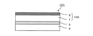
- FIG. 1 is a schematic cross-sectional view showing an embodiment of a transparent conductive film 100, in which a transparent conductive layer 2 is formed on a transparent substrate 1 including a transparent film 11 made of an organic polymer molded product.
- the transparent conductive film 100 is obtained by a base material preparation step of preparing a transparent base material and a film forming step of sputtering a transparent conductive layer made of In / Sn composite oxide (ITO) on the transparent base material.
- ITO In / Sn composite oxide
- the transparent substrate 1 includes a transparent film 11 made of an organic polymer molded product.
- a film excellent in transparency and heat resistance is particularly preferably used.
- organic polymers include polyester polymers such as polyethylene terephthalate, polyolefin polymers, norbornene polymers, single component polymers such as polycarbonate, polyethersulfone, and polyarylate, copolymer polymers, Examples include epoxy polymers.
- a film-like material, a sheet-like material, or other molded products of these organic polymers are preferably used.
- the transparent base material 1 may consist only of the transparent film 11, as shown in FIG. 1, the undercoat layer 12 and the back surface coating layer 13 may be formed on the surface of the transparent film 11. .
- FIG. 1 shows a form in which one undercoat layer 12 and one back coat layer 13 are formed, these layers may be composed of two or more layers.
- the transparent substrate 1 a substrate in which a birefringent layer made of a liquid crystal monomer or a liquid crystal polymer is formed can be used as the transparent substrate 1.
- the arithmetic average roughness Ra of the surface of the transparent substrate 1 on which the transparent conductive layer 2 is formed is preferably 1.0 nm or less, more preferably 0.7 nm or less, and 0.6 nm or less. More preferably, it is particularly preferably 0.5 nm or less.
- the lower limit value of the arithmetic average roughness Ra of the transparent base material surface is not particularly limited, but is preferably 0.1 nm or more from the viewpoint of imparting winding property when the base material is wound into a roll. More preferably.
- the arithmetic average roughness Ra is measured using an atomic force microscope (AFM, Digital Instruments, Nonscope IV).
- a film made of an organic polymer molded product contains a filler and the like in the film from the viewpoint of productivity and handling properties, and therefore the arithmetic average roughness Ra of the surface is often several nm or more.
- the undercoat layer 12 is preferably formed on the surface of the transparent film 11 on the side where the transparent conductive layer 2 is formed. By forming the undercoat layer on the surface of the transparent film, the surface unevenness of the transparent film is alleviated and the surface roughness can be reduced.
- a dielectric having transparency and a surface resistance of, for example, 1 ⁇ 10 6 ⁇ / ⁇ or more is preferably used.
- examples of such a material include inorganic substances such as NaF, Na 3 AlF 6 , LiF, MgF 2 , CaF 2 , BaF 2 , BaF 2 , SiO 2 , LaF 3 , CeF, and Al 2 O 3 , and a refractive index of 1.
- examples thereof include organic substances such as acrylic resin, urethane resin, melamine resin, alkyd resin, siloxane polymer, and organic silane condensate of about 4 to 1.6, or a mixture of the inorganic substance and the organic substance.
- the undercoat layer 12 can be formed by using the above materials by a dry coating method such as a vacuum deposition method, a sputtering method, an ion plating method, a wet coating method (coating method), or the like.
- the undercoat layer 12 is preferably formed by a wet coating method.
- it is preferable that at least 1 layer of them is formed into a film by the wet-coating method.
- the undercoat layer is formed by the wet coating method, the surface unevenness of the transparent film 11 is relaxed and a uniform film is easily formed. Therefore, the arithmetic average roughness Ra of the surface of the transparent substrate 1 is reduced to the predetermined range. be able to.
- the surface of the transparent substrate is subjected to corona discharge treatment, ultraviolet irradiation treatment, plasma treatment, sputter etching in advance.
- An appropriate adhesion treatment such as treatment may be performed.
- an antiglare treatment layer or an antireflection treatment layer for the purpose of improving visibility, or a hard coat treatment layer for the purpose of protecting the outer surface can be provided.
- a hard coat treatment layer a cured film made of a curable resin such as a melamine resin, a urethane resin, an alkyd resin, an acrylic resin, or a silicone resin is preferably used.
- These back coat layers 13 may be provided on the transparent film 11 before the transparent conductive layer 3 is formed. It may be provided after the transparent conductive layer 3 is formed.
- an amorphous transparent conductive layer (amorphous ITO film) 3 made of In / Sn composite oxide is formed on the transparent substrate 1 by a sputtering method.
- the “amorphous ITO” is not limited to a completely amorphous one, and may have a small amount of crystal components. Whether the ITO is amorphous or not is determined by immersing the laminate in which the transparent conductive layer is formed on the base material in hydrochloric acid having a concentration of 5 wt. Can be measured by measuring with a tester. Since the amorphous ITO film disappears by etching with hydrochloric acid, the resistance increases by immersion in hydrochloric acid. In the present specification, ITO is amorphous when the resistance between terminals of 15 mm exceeds 10 k ⁇ after immersion in hydrochloric acid, washing with water, and drying.
- the transparent conductive layer not only a standard magnetron sputtering method using a DC power source but also various sputtering methods such as an RF sputtering method, an RF + DC sputtering method, a pulse sputtering method, and a dual magnetron sputtering method can be employed.
- various sputtering methods such as an RF sputtering method, an RF + DC sputtering method, a pulse sputtering method, and a dual magnetron sputtering method can be employed.
- a sputter target used for sputtering film formation is a metal target (In—Sn target) in which the amount of Sn atoms is more than 6 wt% and not more than 15 wt% with respect to the weight of In and Sn atoms added. Or an oxide target (In 2 O 3 —SnO 2 target).
- the amount of Sn atoms in the sputter target is more preferably 7 to 14% by weight, and still more preferably 8 to 13% by weight, based on the weight of In atoms and Sn atoms added.
- the Sn content in the sputter target is substantially equal to the Sn content in the transparent conductive layer 2, but if the Sn content in the transparent conductive layer is too small, when amorphous ITO is heated and crystallized, The specific resistance is unlikely to be low, and a low-resistance transparent conductive layer may not be obtained.
- Sn acts as an impurity other than the amount taken into the In 2 O 3 crystal lattice and tends to hinder crystallization. For this reason, if the Sn content is too large, it becomes difficult to obtain a fully crystallized ITO film or it takes a long time for crystallization.
- Sputter deposition using such a target is performed by introducing Ar gas, which is an inert gas, into a sputtering apparatus evacuated to high vacuum.
- Ar gas which is an inert gas
- an oxidizing agent such as oxygen gas is introduced together with the Ar gas to perform reactive sputtering film formation.
- oxygen gas or the like may be introduced in addition to Ar gas.
- the partial pressure of water during film formation is preferably 0.1% or less, more preferably 0.07% or less with respect to the partial pressure of Ar gas.
- the partial pressure of water during film formation is preferably 2 ⁇ 10 ⁇ 4 Pa or less, more preferably 1.5 ⁇ 10 ⁇ 4 Pa or less, and 1 ⁇ 10 ⁇ 4 Pa or less. It is preferable.
- the inside of the sputtering apparatus is 2 ⁇ 10 ⁇ 4 Pa or less, preferably 1.5 ⁇ , so that the partial pressure of water is within the above range before the start of film formation. It is preferable to evacuate to 10 ⁇ 4 Pa or less, more preferably 1 ⁇ 10 ⁇ 4 Pa or less, to create an atmosphere in which impurities such as moisture in the apparatus and organic gas generated from the substrate are removed.
- the substrate temperature during sputtering film formation exceeds 100 ° C.
- the base material temperature is more preferably 120 ° C. or more, and 130 ° C. or more from the viewpoint of forming a low-resistance crystalline transparent conductive layer. It is more preferable that the temperature is 140 ° C. or higher.
- the substrate temperature is preferably 200 ° C. or less, more preferably 180 ° C. or less, further preferably 170 ° C. or less, and particularly preferably 160 ° C. or less.
- the “base material temperature” is a set temperature of the base material of the base material during sputtering film formation.
- the base material temperature in the case of continuously performing the sputtering film formation by the roll sputtering apparatus is the temperature of the can roll at which the sputtering film formation is performed.
- the base material temperature in the case of performing single-wafer type (batch type) sputtering film formation is the temperature of the base material holder for placing the base material.
- the film thickness of the transparent conductive layer during sputtering film formation is preferably 15 to 50 nm, and more preferably 20 to 30 nm. If the film thickness of the amorphous transparent conductive layer is excessively small, the ITO film tends to be difficult to crystallize in the subsequent heat treatment step. When the film thickness exceeds 30 nm, when the transparent conductive layer is crystallized, the resistance is too low, or the transparency and flexibility of the transparent conductive film are lowered, resulting in poor quality when used for touch panels. There is a case.
- the amorphous transparent conductive layer formed by sputtering on the substrate preferably has a hole mobility of 5 to 30 cm 2 / V ⁇ s and a carrier density of 1 ⁇ 10 20 to 10 ⁇ 10 20 / cm. 3 is preferred. Further, by employing the film forming conditions as described above, the hole mobility and the carrier density can be within the above ranges.
- the transparent conductive film thus obtained can be used as it is for a touch panel as it is, but it is subjected to a heat treatment step to heat the amorphous ITO film to form a crystalline transparent conductive layer (crystalline ITO film). It can also be converted.
- the transparent conductive layer may be patterned into a predetermined shape (for example, a strip shape).
- a predetermined shape for example, a strip shape.
- the ITO film is crystallized by heat treatment, etching with acid becomes difficult.
- the amorphous ITO film before the heat treatment can be easily etched. Therefore, when patterning a transparent conductive layer by etching, it is preferable to carry out after forming a transparent conductive layer and before a heat treatment process.
- the heat treatment step is a step of heating and crystallizing the amorphous transparent conductive layer after the sputtering film formation.
- the heating temperature and the heating time are appropriately selected so that ITO of the transparent conductive layer is completely crystallized.
- complete crystallization refers to a state where grains crystallized by observation with a transmission electron microscope (TEM) are present on the entire surface.
- the heating temperature in the heat treatment step is preferably 120 ° C to 160 ° C, more preferably 125 ° C to 160 ° C, and further preferably 130 ° C to 160 ° C.
- the heating time is preferably 120 minutes or less, more preferably 90 minutes or less, and even more preferably 60 minutes or less.
- the heating time is preferably 30 minutes or more.
- an ITO film in which the Sn content exceeds 6% by weight with respect to the weight of In and Sn atoms is difficult to crystallize. It was necessary to heat for more than an hour.
- the ITO film can be completely crystallized under relatively low temperature and short heating conditions.
- the hole mobility of the transparent conductive layer changes greatly before and after the crystallization. Without any significant increase in carrier density. That is, the hole mobility after crystallization is about 5 to 35 cm 2 / V ⁇ s, which is not significantly changed from about 5 to 30 cm 2 / V ⁇ s before crystallization.
- the carrier density after crystallization is about 6 ⁇ 10 20 to 15 ⁇ 10 20 / cm 3, which is significantly increased from about 1 ⁇ 10 20 to 10 ⁇ 10 20 / cm 3 before crystallization, This is presumed to contribute to the reduction in resistance.
- the carrier density of the crystalline transparent conductive layer after the heat treatment step is higher than that of the amorphous transparent conductive layer before the heat treatment step. It is preferable to increase.
- the carrier density is more preferably increased 1.5 times or more, and more preferably 2 times or more.
- the transparent conductive film obtained by the above process can be used as it is for various applications such as a touch panel.
- a transparent substrate 4 is bonded to a surface of the transparent substrate 1 opposite to the surface on which the transparent conductive layer 2 is formed, with a transparent adhesive layer 3 interposed therebetween, and transparent conductive It can also be set as the laminated body 101.
- the transparent substrate 4 may be bonded to the transparent conductive film 100 by providing the pressure-sensitive adhesive layer 3 on the transparent substrate 4 and bonding the transparent conductive film 100 (to the transparent substrate 1 side) thereto.
- the pressure-sensitive adhesive layer 3 may be provided on the transparent conductive film 100 (on the transparent substrate 1 side), and the transparent substrate 4 may be bonded thereto.
- the latter method is more advantageous in terms of productivity because the transparent conductive film can be rolled to continuously form the pressure-sensitive adhesive layer.
- the pressure-sensitive adhesive layer can be used without particular limitation as long as it has transparency.
- an acrylic adhesive, a silicone adhesive, a rubber adhesive, or the like is used.
- This pressure-sensitive adhesive layer has a function of improving the scratch resistance of the transparent conductive layer and the dot characteristics for touch panels by the cushion effect after the transparent substrate is bonded.
- the transparent substrate bonded through such an adhesive layer gives good mechanical strength to the film substrate, and can contribute to prevention of curling and the like.
- a plastic film with a thickness of about 6 to 300 ⁇ m is usually used as the transparent substrate.
- a glass plate of about 05 to 10 mm or a film or plate-like plastic is used. Examples of the plastic material include the same materials as those described above.
- the transparent conductive film thus produced is suitably used for forming transparent electrodes and touch panels of various devices.
- the ITO film has a low resistance
- the transparent conductive film obtained by the present invention can be suitably used for a touch panel of a display device that requires a large screen and high response characteristics.
- the transparent conductive film of the present invention has excellent moisture and heat resistance, it can be suitably used for various applications in which it is desired to have excellent environmental resistance at high temperature and high humidity in addition to the touch panel. .
- the total light transmittance was measured according to JIS K7105 using a haze meter (manufactured by Suga Test Instruments).
- the surface resistance ( ⁇ / ⁇ ) of the ITO film was determined by the four probe method. Further, after immersing the transparent conductive film in hydrochloric acid having a concentration of 5 wt% for 15 minutes, the surface resistance after washing and drying was measured to confirm the presence or absence of crystallization.
- Example 1 (Preparation of transparent substrate) A heat of a 2: 2: 1 weight ratio of a condensate of melamine resin: alkyd resin: organosilane as an undercoat layer on one surface of a film substrate made of a polyethylene terephthalate film (hereinafter referred to as PET film) having a thickness of 23 ⁇ m. A curable resin was formed to a thickness of 35 nm. The arithmetic average roughness Ra of the undercoat layer surface was 0.5 nm.
- Transparent conductive layer deposition On this undercoat layer, reactive sputtering using a sintered body material of 90 wt% indium oxide and 10 wt% tin oxide in an atmosphere of 0.4 Pa composed of 98 vol% argon gas and 2 vol% oxygen gas.
- a transparent conductive thin film (hereinafter referred to as ITO film) made of indium-tin composite oxide having a thickness of 25 nm was formed.
- the inside of the sputtering apparatus was evacuated until the partial pressure of water during film formation became 8.0 ⁇ 10 ⁇ 5 Pa, and then argon gas and oxygen gas were introduced, the substrate temperature was 140 ° C., moisture Film formation was performed in an atmosphere with a pressure of 8.0 ⁇ 10 ⁇ 5 Pa. The partial pressure of water at this time was 0.05% with respect to the partial pressure of argon gas.
- the transparent conductive layer of the transparent conductive film thus obtained was observed with a transmission electron microscope (TEM) at a magnification of 25,000 times, it was not completely crystallized.
- TEM transmission electron microscope
- the resistance value is ⁇ , which indicates that the ITO film is amorphous.
- the transparent conductive film having an amorphous ITO film formed on the transparent substrate was subjected to a heat treatment at 140 ° C. for 90 minutes to crystallize the ITO film.
- TEM transmission electron microscope
- Example 2 Except for the film formation of the transparent conductive layer of Example 1, except that the film was formed by introducing argon gas and oxygen gas after exhausting until the water pressure became 2.0 ⁇ 10 ⁇ 4 Pa. Similarly, after forming a transparent conductive thin film on a transparent substrate, a heat treatment was performed at 140 ° C. for 120 minutes to obtain a transparent conductive film on which a completely crystallized ITO film was formed on the transparent substrate. . The partial pressure of water during film formation was 2.0 ⁇ 10 ⁇ 4 Pa, which was 0.10% with respect to the partial pressure of argon gas.
- Example 3 In forming the transparent conductive layer of Example 1, after forming a transparent conductive thin film on the transparent substrate in the same manner as in Example 1 except that the substrate temperature was 120 ° C., 140 ° C. for 90 minutes. Heat treatment was performed to obtain a transparent conductive film on which a fully crystallized ITO film was formed on a transparent substrate.
- Example 1 In forming the transparent conductive layer of Example 1, instead of using a sintered body material of 90% by weight of indium oxide and 10% of tin oxide, a sintered body material of 97% by weight of indium oxide and 3% by weight of tin oxide was used. It was. Others were carried out similarly to Example 1, and after forming the transparent conductive layer on the transparent base material, it heat-processed and the transparent conductive film in which the ITO film
- Example 2 In the production of the transparent substrate of Example 1, instead of forming a thermosetting resin layer as an undercoat layer on one surface of the PET film, a SiO 2 undercoat layer having a film thickness of 30 nm was formed by vacuum deposition. . The arithmetic average roughness Ra of the surface of the transparent substrate on which the undercoat layer is formed was 2.0 nm. A transparent conductive layer was formed on the undercoat layer in the same manner as in Example 1, and then a heat treatment was performed at 140 ° C. for 120 minutes to obtain a transparent conductive film.
- Example 3 Except for the film formation of the transparent conductive layer of Example 1 except that the film was formed by introducing argon gas and oxygen gas after exhausting until the water pressure became 4.0 ⁇ 10 ⁇ 4 Pa. Similarly, after forming a transparent conductive thin film on a transparent substrate, a heat treatment was performed at 140 ° C. for 120 minutes to obtain a transparent conductive film on which a completely crystallized ITO film was formed on the transparent substrate. . The partial pressure of water at the time of film formation was 4.0 ⁇ 10 ⁇ 4 Pa, which was 0.20% with respect to the partial pressure of argon gas.
- Example 4 In forming the transparent conductive layer of Example 1, after forming the transparent conductive thin film on the transparent substrate in the same manner as in Example 1 except that the substrate temperature during film formation was 80 ° C., A heat treatment was performed at 140 ° C. for 120 minutes to obtain a transparent conductive film in which a completely crystallized ITO film was formed on a transparent substrate.
- Table 1 shows the production conditions of the above Examples and Comparative Examples and the evaluation results of the transparent conductive film.
- Example 1 the surface resistance of the ITO film was reduced to 1/3 or less due to crystallization, and a low-resistance crystalline ITO film was obtained. This is presumed to be caused by a significant increase in carrier density during crystallization. Furthermore, in Examples 1 to 3, the total light transmittance increased by 2% or more before and after the heating step, indicating that a transparent conductive film having high transparency can be obtained.
- Comparative Example 1 using a sputter target with a small tin content, the ITO film was completely crystallized by the same heat treatment as in Example 1, but the surface resistance after crystallization was about 60% before crystallization. Thus, a low-resistance ITO film has not been obtained.
- the hole mobility is increased by about 1.5 times as compared with that before crystallization, whereas the carrier density is reduced, which is lower in resistance than Examples 1 to 3. It is thought that the mechanism of crystallization is different.
- Comparative Example 2 using a transparent substrate having a large Ra, although the film formation and the heat treatment were performed under the same conditions as in Example 1, the amount of decrease in surface resistance after heating was small. Moreover, in the comparative example 2, the surface resistance after immersing the transparent conductive film after a heating in hydrochloric acid is infinity, and crystallization is not enough. From the comparison between Example 1 and Comparative Example 2, by reducing the arithmetic average roughness Ra of the surface of the transparent substrate on which the transparent conductive layer is formed, a low resistance crystallized ITO film can be obtained by heating in a short time. It turns out that it is obtained.
- Comparative Example 4 where the base material temperature at the time of forming the ITO film is as low as 80 ° C., the resistance is reduced as compared with Comparative Examples 1 and 2, but the resistance reduction as in Examples 1 to 3 is achieved. Not. Moreover, in the comparative example 4, the surface resistance after immersing the transparent conductive film after a heating in hydrochloric acid is infinity, and crystallization is not enough.
- a transparent conductive film in which a crystalline ITO film is formed on a transparent substrate can be efficiently produced and obtained. It can be seen that the crystalline ITO film has a low resistance because it has a high carrier density.
Landscapes
- Chemical & Material Sciences (AREA)
- Chemical Kinetics & Catalysis (AREA)
- Engineering & Computer Science (AREA)
- Materials Engineering (AREA)
- Mechanical Engineering (AREA)
- Metallurgy (AREA)
- Organic Chemistry (AREA)
- Physics & Mathematics (AREA)
- Thermal Sciences (AREA)
- Non-Insulated Conductors (AREA)
- Manufacturing Of Electric Cables (AREA)
- Physical Vapour Deposition (AREA)
- Laminated Bodies (AREA)
Abstract
Description
透明基材1は、有機高分子成型物からなる透明フィルム11を含む。透明フィルム11としては、特に、透明性や耐熱性にすぐれたものが好適に用いられる。このような有機高分子としては、ポリエチレンテレフタレートなどのポリエステル系高分子、ポリオレフィン系高分子、ノルボルネン系高分子、ポリカーボネート、ポリエーテルスルフォン、ポリアリレートなどの単一成分の高分子、共重合高分子、エポキシ系高分子などが挙げられる。透明フィルム11は、これら有機高分子のフィルム状物、シート状物、その他の成型物が好適に用いられる。
製膜工程においては、透明基材1上にIn・Sn複合酸化物からなるアモルファス透明導電層(アモルファスITO膜)3がスパッタ法により製膜される。なお、「アモルファスITO」とは、完全に非晶質であるものに限られず、少量の結晶成分を有していてもよい。ITOがアモルファスであるか否かの判定は、基材上に透明当電層が形成された積層体を濃度5wt%の塩酸に15分間浸漬した後、水洗・乾燥し、15mm間の端子間抵抗をテスタにて測定することにより行い得る。アモルファスITO膜は塩酸によりエッチングされて消失するために、塩酸への浸漬により抵抗が増大する。本明細書においては、塩酸への浸漬・水洗・乾燥後に、15mm間の端子間抵抗が10kΩを超える場合に、ITOがアモルファスであるものとする。
熱処理工程は、スパッタ製膜後のアモルファス透明導電層を加熱して結晶化する工程である。加熱温度および加熱時間は、透明導電層のITOが完全結晶化するように適宜に選択される。ここで、「完全結晶化」とは、透過型電子顕微鏡(TEM)観察により結晶化したグレインが全面に存在する状態を指す。
原子間力顕微鏡(AFM Digital Instruments社 Nanscope IV」)を用いて測定した。
ホール効果測定システム(バイオラッド製 商品名「HL5500PC」)を用い、熱処理工程前(スパッタ直後)および熱処理工程後の透明導電層ホール移動度およびキャリア密度を測定した。
ヘイズメーター(スガ試験機製)を用いて、JIS K7105に準じ、全光線透過率を測定した。
ITO膜の表面抵抗(Ω/□)は四端子法により求めた。また、透明導電性フィルムを濃度5wt%の塩酸に15分間浸漬した後、水洗・乾燥した後の表面抵抗を測定して、結晶化の有無を確認した。
(透明基材の作製)
厚みが23μmのポリエチレンテレフタレートフィルム(以下、PETフィルム)からなるフィルム基材の一方の面に、アンダーコート層として、メラミン樹脂:アルキド樹脂:有機シランの縮合物の重量比2:2:1の熱硬化型樹脂を厚みが35nmとなるように形成した。アンダーコート層表面の算術平均粗さRaは、0.5nmであった。
このアンダーコート層上に、アルゴンガス98体積%と酸素ガス2体積%からなる0.4Paの雰囲気中で、酸化インジウム90重量%-酸化スズ10重量%の焼結体材料を用いた反応性スパッタリング法により、厚みが25nmのインジウム・スズ複合酸化物からなる透明導電性薄膜(以下、ITO膜)を形成した。製膜に際しては、スパッタ装置内を製膜時の水の分圧が、8.0×10⁻⁵Paとなるまで排気した後、アルゴンガスおよび酸素ガスを導入し、基材温度140℃、水分圧が8.0×10⁻⁵Paの雰囲気にて製膜を行った。この時の水の分圧は、アルゴンガスの分圧に対して0.05%であった。
上記の透明基材上にアモルファスITO膜が形成された透明導電性フィルムを140℃で90分間加熱する熱処理を行い、ITO膜の結晶化を行った。熱処理後の透明導電性フィルムの透明導電層を倍率25000倍の透過型電子顕微鏡(TEM)観察したところ、ITO膜が完全結晶化していることが分かった。また、表1に示すように、塩酸への浸漬後の抵抗値に変化がみられなくなっており、酸によってエッチング加工されない結晶性ITO膜が形成されていることがわかる。
実施例1の透明導電層の製膜において、水分圧が2.0×10⁻⁴Paとなるまで排気した後にアルゴンガスおよび酸素ガスを導入して製膜を行った以外は、実施例1と同様にして、透明基材上に透明導電性薄膜を製膜した後、140℃120分の熱処理を行い、透明基材上に完全結晶化したITO膜が形成された透明導電性フィルムを得た。製膜時の水の分圧は2.0×10⁻⁴Paであり、アルゴンガスの分圧に対して0.10%であった。
実施例1の透明導電層の製膜において、基材温度を120℃とした以外は実施例1と同様にして、透明基材上に透明導電性薄膜を製膜した後、140℃90分の熱処理を行い、透明基材上に完全結晶化したITO膜が形成された透明導電性フィルムを得た。
実施例1の透明導電層の製膜において、酸化インジウム90重量%-酸化スズ10%の焼結体材料を用いる代わりに、酸化インジウム97重量%-酸化スズ3重量%の焼結体材料を用いた。その他は実施例1と同様にして、透明基材上に透明導電層を製膜した後、熱処理を行い、透明基材上に完全結晶化したITO膜が形成された透明導電性フィルムを得た。
実施例1の透明基材の作製において、PETフィルムの一方の面に、アンダーコート層として熱硬化型樹脂層を形成する代わりに、真空蒸着法により膜厚30nmのSiO2アンダーコート層を形成した。この透明基材のアンダーコート層が形成されている側の面の算術平均粗さRaは、2.0nmであった。このアンダーコート層上に、実施例1と同様にして、透明導電層を製膜した後、140℃120分の熱処理を行い、透明導電性フィルムを得た。
実施例1の透明導電層の製膜において、水分圧が4.0×10⁻⁴Paとなるまで排気した後にアルゴンガスおよび酸素ガスを導入して製膜を行った以外は、実施例1と同様にして、透明基材上に透明導電性薄膜を製膜した後、140℃120分の熱処理を行い、透明基材上に完全結晶化したITO膜が形成された透明導電性フィルムを得た。製膜時の水の分圧は4.0×10⁻⁴Paであり、アルゴンガスの分圧に対して0.20%であった。
実施例1の透明導電層の製膜において、製膜時の基材温度を80℃とした以外は、実施例1と同様にして、透明基材上に透明導電性薄膜を製膜した後、140℃120分の熱処理を行い、透明基材上に完全結晶化したITO膜が形成された透明導電性フィルムを得た。

11 透明フィルム
12 アンダーコート層
13 背面コート層
2 透明導電層
3 粘着剤層
4 透明基体
100 透明導電性フィルム
101 透明導電性積層体
Claims (9)
- 透明基材を準備する基材準備工程、および前記透明基材上にIn・Sn複合酸化物からなる透明導電層をスパッタ製膜する製膜工程、を有する透明導電性フィルムの製造方法であって、
前記透明基材の透明導電層を形成する側の面の算術平均粗さRaが1.0nm以下であり、
前記製膜工程において、
Sn原子の量が、In原子とSn原子とを加えた重さに対し、6重量%を超え15重量%以下であるメタルターゲットまたは酸化物ターゲットを用い、
水の分圧がArガスの分圧に対して0.1%以下の雰囲気下で、基材温度が100℃を超え200℃以下でスパッタ製膜することにより、
In・Sn複合酸化物からなるアモルファス透明導電層を形成する、
透明導電性フィルムの製造方法。 - 前記製膜工程における水の分圧が2×10⁻⁴Pa以下である請求項1に記載の透明導電性フィルムの製造方法。
- 前記アモルファス透明導電層のホール移動度が5~30cm2/V・sであり、キャリア密度が1×1020~10×1020/cm3である、請求項1または2に記載の透明導電性フィルムの製造方法。
- 前記製膜工程において、膜厚が15~50nmとなるように、透明導電層が形成される、請求項1~3のいずれか1項に記載の透明導電性フィルムの製造方法。
- さらに、前記アモルファス透明導電層を加熱して結晶性透明導電層に転化する熱処理工程を有する、請求項1~4のいずれか1項に記載の透明導電性フィルムの製造方法。
- 前記熱処理工程において、転化前のアモルファス透明導電層に比して結晶性透明導電層のキャリア密度が増加することを特徴とする、請求項5に記載の透明導電性フィルムの製造方法。
- 前記結晶性透明導電層のホール移動度が10~35cm2/V・sであり、キャリア密度が6×1020~15×1020/cm3である、請求項5または6に記載の透明導電性フィルムの製造方法。
- 透明基材上にIn・Sn複合酸化物からなる透明導電層を有する透明導電性フィルムであって、
前記透明基材の透明導電層が形成されている側の表面の算術平均粗さRaが1.0nm以下であり、
前記透明導電層中のSn原子の量が、In原子とSn原子とを加えた重さに対し、6重量%を超え15重量%以下であり、
前記透明導電層のホール移動度が10~35cm2/V・sであり、キャリア密度が6×1020~15×1020/cm3である、透明導電性フィルム。 - 前記透明導電層の膜厚が15~50nmである、請求項8に記載の透明導電性フィルム。
Priority Applications (4)
| Application Number | Priority Date | Filing Date | Title |
|---|---|---|---|
| CN201180062582.0A CN103282539B (zh) | 2010-12-24 | 2011-12-14 | 透明导电性薄膜及其制造方法 |
| KR1020137019480A KR20130099213A (ko) | 2010-12-24 | 2011-12-14 | 투명 도전성 필름 및 그 제조 방법 |
| US13/997,466 US20130288047A1 (en) | 2010-12-24 | 2011-12-14 | Transparent conductive film and manufacturing method therefor |
| KR20157004061A KR20150027845A (ko) | 2010-12-24 | 2011-12-14 | 투명 도전성 필름 및 그 제조 방법 |
Applications Claiming Priority (2)
| Application Number | Priority Date | Filing Date | Title |
|---|---|---|---|
| JP2010286948A JP5543907B2 (ja) | 2010-12-24 | 2010-12-24 | 透明導電性フィルムおよびその製造方法 |
| JP2010-286948 | 2010-12-24 |
Publications (1)
| Publication Number | Publication Date |
|---|---|
| WO2012086484A1 true WO2012086484A1 (ja) | 2012-06-28 |
Family
ID=46313760
Family Applications (1)
| Application Number | Title | Priority Date | Filing Date |
|---|---|---|---|
| PCT/JP2011/078875 Ceased WO2012086484A1 (ja) | 2010-12-24 | 2011-12-14 | 透明導電性フィルムおよびその製造方法 |
Country Status (6)
| Country | Link |
|---|---|
| US (1) | US20130288047A1 (ja) |
| JP (1) | JP5543907B2 (ja) |
| KR (2) | KR20150027845A (ja) |
| CN (1) | CN103282539B (ja) |
| TW (1) | TWI607099B (ja) |
| WO (1) | WO2012086484A1 (ja) |
Cited By (3)
| Publication number | Priority date | Publication date | Assignee | Title |
|---|---|---|---|---|
| WO2015178297A1 (ja) * | 2014-05-20 | 2015-11-26 | 日東電工株式会社 | 透明導電性フィルム |
| WO2016088807A1 (ja) * | 2014-12-05 | 2016-06-09 | 日東電工株式会社 | 透明導電性フィルムおよびそれを用いたタッチセンサ |
| JP2019188658A (ja) * | 2018-04-23 | 2019-10-31 | 東洋紡株式会社 | 積層フィルム |
Families Citing this family (43)
| Publication number | Priority date | Publication date | Assignee | Title |
|---|---|---|---|---|
| TWI544500B (zh) * | 2011-12-27 | 2016-08-01 | Sekisui Chemical Co Ltd | Transparent conductive film and electrostatic capacity type touch panel having the same, and a method for manufacturing a translucent conductive film |
| CN103999166B (zh) * | 2012-06-07 | 2018-01-09 | 日东电工株式会社 | 透明导电性膜 |
| KR101509289B1 (ko) | 2012-09-07 | 2015-04-06 | (주)엘지하우시스 | 낮은 면저항을 가지는 투명 도전성 필름 및 이의 제조방법 |
| KR101572712B1 (ko) | 2012-11-21 | 2015-11-27 | (주)엘지하우시스 | 투명 도전성 필름 및 이의 제조방법 |
| US9903015B2 (en) | 2012-12-19 | 2018-02-27 | Kaneka Corporation | Substrate with transparent electrode and method for manufacturing same |
| WO2014115770A1 (ja) * | 2013-01-24 | 2014-07-31 | 住友金属鉱山株式会社 | 透明導電性基材ならびにその製造方法 |
| JP5805799B2 (ja) * | 2013-05-15 | 2015-11-10 | 日本写真印刷株式会社 | タッチセンサおよびタッチセンサモジュール |
| US10270010B2 (en) | 2014-01-28 | 2019-04-23 | Kaneka Corporation | Substrate with transparent electrode and method for producing same |
| JP6524068B2 (ja) | 2014-03-28 | 2019-06-05 | 株式会社カネカ | 透明導電フィルムおよびその製造方法 |
| WO2015159804A1 (ja) * | 2014-04-15 | 2015-10-22 | 旭硝子株式会社 | 積層体、導電性積層体、および電子機器 |
| JP5932098B2 (ja) * | 2014-04-17 | 2016-06-08 | 日東電工株式会社 | 透明導電性フィルム |
| JP6211557B2 (ja) * | 2014-04-30 | 2017-10-11 | 日東電工株式会社 | 透明導電性フィルム及びその製造方法 |
| WO2015166723A1 (ja) * | 2014-04-30 | 2015-11-05 | 日東電工株式会社 | 透明導電性フィルム |
| WO2015178298A1 (ja) * | 2014-05-20 | 2015-11-26 | 日東電工株式会社 | 透明導電性フィルムおよびその製造方法 |
| TWI549030B (zh) * | 2014-10-20 | 2016-09-11 | Far Eastern New Century Corp | Conductive transparent laminates, patterned conductive transparent laminates and touch panels |
| KR101595309B1 (ko) * | 2014-11-28 | 2016-02-19 | (주)알에프트론 | 주석 금속 타겟을 이용한 주석산화물층의 형성 방법 |
| JP6661335B2 (ja) * | 2014-12-22 | 2020-03-11 | 日東電工株式会社 | 透明導電性フィルム |
| KR101667658B1 (ko) | 2014-12-30 | 2016-10-19 | 코오롱글로텍주식회사 | 플렉서블 전도성 패브릭 기판 및 그의 제조방법 |
| JP5860558B1 (ja) * | 2015-03-20 | 2016-02-16 | 積水化学工業株式会社 | 光透過性導電性フィルム及びそれを有するタッチパネル |
| WO2017014307A1 (ja) * | 2015-07-23 | 2017-01-26 | 富士フイルム株式会社 | 積層体 |
| JP6159490B1 (ja) * | 2015-09-30 | 2017-07-05 | 積水化学工業株式会社 | 光透過性導電フィルム、及び、アニール処理された光透過性導電フィルムの製造方法 |
| CN105226016B (zh) * | 2015-10-14 | 2018-11-23 | 京东方科技集团股份有限公司 | 阵列基板及其制作方法 |
| WO2017082229A1 (ja) * | 2015-11-09 | 2017-05-18 | 日東電工株式会社 | 光透過性導電フィルムおよび調光フィルム |
| JP6412539B2 (ja) * | 2015-11-09 | 2018-10-24 | 日東電工株式会社 | 光透過性導電フィルムおよび調光フィルム |
| JP6654865B2 (ja) | 2015-11-12 | 2020-02-26 | 日東電工株式会社 | 非晶質透明導電性フィルム、ならびに、結晶質透明導電性フィルムおよびその製造方法 |
| JP6392912B2 (ja) * | 2017-01-31 | 2018-09-19 | 学校法人東海大学 | 成膜方法 |
| KR20190042438A (ko) * | 2017-10-16 | 2019-04-24 | 닛토덴코 가부시키가이샤 | 무기물층 적층체의 제조 방법 |
| CN108595043B (zh) * | 2018-03-20 | 2021-11-05 | 黄石瑞视光电技术股份有限公司 | 一种适于低压环境的触摸屏及其制造方法 |
| KR20190123081A (ko) | 2018-04-23 | 2019-10-31 | 도레이첨단소재 주식회사 | 투명 도전성 필름 |
| JP2019200910A (ja) * | 2018-05-16 | 2019-11-21 | 日東電工株式会社 | 透明導電性ガラス |
| JP7116994B2 (ja) * | 2018-06-27 | 2022-08-12 | ロック技研工業株式会社 | Itoフィルム及び透明導電性フィルム |
| JP7162462B2 (ja) * | 2018-08-02 | 2022-10-28 | 日東電工株式会社 | ヒータ及びヒータ付物品 |
| JP7280036B2 (ja) * | 2018-12-17 | 2023-05-23 | 日東電工株式会社 | 導電性フィルムの製造方法 |
| JP7198096B2 (ja) * | 2019-01-30 | 2022-12-28 | 日東電工株式会社 | 透明導電性フィルム |
| JP7424750B2 (ja) * | 2019-02-06 | 2024-01-30 | 日東電工株式会社 | 温度センサフィルム、導電フィルムおよびその製造方法 |
| JP7378938B2 (ja) * | 2019-02-22 | 2023-11-14 | 日東電工株式会社 | 光透過性導電フィルム |
| JP7287802B2 (ja) * | 2019-03-14 | 2023-06-06 | 日東電工株式会社 | 光透過性導電フィルム |
| TW202042254A (zh) | 2019-02-22 | 2020-11-16 | 日商日東電工股份有限公司 | 透光性導電膜 |
| JP2020167047A (ja) * | 2019-03-29 | 2020-10-08 | 日東電工株式会社 | ヒータ |
| KR102118859B1 (ko) * | 2019-05-27 | 2020-06-29 | 코오롱인더스트리 주식회사 | 투명전극 및 그 제조방법 |
| KR20220155279A (ko) * | 2020-03-19 | 2022-11-22 | 닛토덴코 가부시키가이샤 | 투명 도전성 필름의 제조 방법 |
| CN116848595A (zh) * | 2021-09-17 | 2023-10-03 | 日东电工株式会社 | 透明导电性薄膜 |
| CN118571991B (zh) * | 2024-08-02 | 2025-01-10 | 安徽光势能新能源科技有限公司 | 一种提升电池片与胶膜的粘结力的方法 |
Citations (4)
| Publication number | Priority date | Publication date | Assignee | Title |
|---|---|---|---|---|
| JPH0864034A (ja) * | 1994-08-26 | 1996-03-08 | Teijin Ltd | 透明導電性積層体 |
| JP2003297150A (ja) * | 2002-04-08 | 2003-10-17 | Nitto Denko Corp | 透明導電積層体とその製造方法 |
| JP2006019239A (ja) * | 2004-06-03 | 2006-01-19 | Nitto Denko Corp | 透明導電性フィルム |
| JP2009104842A (ja) * | 2007-10-22 | 2009-05-14 | Nitto Denko Corp | 透明導電性フィルム、その製造方法及びそれを備えたタッチパネル |
Family Cites Families (3)
| Publication number | Priority date | Publication date | Assignee | Title |
|---|---|---|---|---|
| JP2004039469A (ja) * | 2002-07-04 | 2004-02-05 | Konica Minolta Holdings Inc | 透明導電性薄膜の形成方法、透明導電性物品及び透明導電性フィルム |
| CN100460943C (zh) * | 2004-06-03 | 2009-02-11 | 日东电工株式会社 | 透明导电性膜 |
| JP5432501B2 (ja) * | 2008-05-13 | 2014-03-05 | 日東電工株式会社 | 透明導電フィルム及びその製造方法 |
-
2010
- 2010-12-24 JP JP2010286948A patent/JP5543907B2/ja active Active
-
2011
- 2011-12-14 US US13/997,466 patent/US20130288047A1/en not_active Abandoned
- 2011-12-14 WO PCT/JP2011/078875 patent/WO2012086484A1/ja not_active Ceased
- 2011-12-14 KR KR20157004061A patent/KR20150027845A/ko not_active Ceased
- 2011-12-14 KR KR1020137019480A patent/KR20130099213A/ko not_active Ceased
- 2011-12-14 CN CN201180062582.0A patent/CN103282539B/zh not_active Expired - Fee Related
- 2011-12-19 TW TW100147182A patent/TWI607099B/zh not_active IP Right Cessation
Patent Citations (4)
| Publication number | Priority date | Publication date | Assignee | Title |
|---|---|---|---|---|
| JPH0864034A (ja) * | 1994-08-26 | 1996-03-08 | Teijin Ltd | 透明導電性積層体 |
| JP2003297150A (ja) * | 2002-04-08 | 2003-10-17 | Nitto Denko Corp | 透明導電積層体とその製造方法 |
| JP2006019239A (ja) * | 2004-06-03 | 2006-01-19 | Nitto Denko Corp | 透明導電性フィルム |
| JP2009104842A (ja) * | 2007-10-22 | 2009-05-14 | Nitto Denko Corp | 透明導電性フィルム、その製造方法及びそれを備えたタッチパネル |
Cited By (8)
| Publication number | Priority date | Publication date | Assignee | Title |
|---|---|---|---|---|
| WO2015178297A1 (ja) * | 2014-05-20 | 2015-11-26 | 日東電工株式会社 | 透明導電性フィルム |
| JPWO2015178297A1 (ja) * | 2014-05-20 | 2017-04-20 | 日東電工株式会社 | 透明導電性フィルムの製造方法 |
| US20190233939A1 (en) * | 2014-05-20 | 2019-08-01 | Nitto Denko Corporation | Transparent conductive film |
| WO2016088807A1 (ja) * | 2014-12-05 | 2016-06-09 | 日東電工株式会社 | 透明導電性フィルムおよびそれを用いたタッチセンサ |
| JP2016110831A (ja) * | 2014-12-05 | 2016-06-20 | 日東電工株式会社 | 透明導電性フィルムおよびそれを用いたタッチセンサ |
| US10217543B2 (en) | 2014-12-05 | 2019-02-26 | Nitto Denko Corporation | Transparent electroconductive film and touch sensor in which same is used |
| JP2019188658A (ja) * | 2018-04-23 | 2019-10-31 | 東洋紡株式会社 | 積層フィルム |
| JP7073882B2 (ja) | 2018-04-23 | 2022-05-24 | 東洋紡株式会社 | 積層フィルム |
Also Published As
| Publication number | Publication date |
|---|---|
| CN103282539B (zh) | 2016-06-29 |
| US20130288047A1 (en) | 2013-10-31 |
| TWI607099B (zh) | 2017-12-01 |
| KR20150027845A (ko) | 2015-03-12 |
| KR20130099213A (ko) | 2013-09-05 |
| TW201233827A (en) | 2012-08-16 |
| CN103282539A (zh) | 2013-09-04 |
| JP2012134085A (ja) | 2012-07-12 |
| JP5543907B2 (ja) | 2014-07-09 |
Similar Documents
| Publication | Publication Date | Title |
|---|---|---|
| JP5543907B2 (ja) | 透明導電性フィルムおよびその製造方法 | |
| US9588606B2 (en) | Transparent conductive film and manufacturing method therefor | |
| EP2450467B1 (en) | Transparent conductive film, method for production thereof and touch panel therewith | |
| WO2013111681A1 (ja) | 透明電極付き基板およびその製造方法 | |
| WO2017131202A1 (ja) | 導電性積層フィルム | |
| CN111613365A (zh) | 透光性导电薄膜 | |
| JP2023160846A (ja) | 光透過性導電フィルム | |
| JP7198097B2 (ja) | 透明導電性フィルム | |
| JP7466269B2 (ja) | 透明導電性フィルムおよび結晶性透明導電性フィルム | |
| JP6097117B2 (ja) | 積層体およびフイルム | |
| JP7378938B2 (ja) | 光透過性導電フィルム | |
| JP7198096B2 (ja) | 透明導電性フィルム | |
| WO2025192641A1 (ja) | 積層圧電体及びタッチパネル | |
| WO2025192633A1 (ja) | 積層圧電体及びその製造方法 | |
| WO2023042848A1 (ja) | 透明導電性フィルム |
Legal Events
| Date | Code | Title | Description |
|---|---|---|---|
| 121 | Ep: the epo has been informed by wipo that ep was designated in this application |
Ref document number: 11850450 Country of ref document: EP Kind code of ref document: A1 |
|
| NENP | Non-entry into the national phase |
Ref country code: DE |
|
| WWE | Wipo information: entry into national phase |
Ref document number: 13997466 Country of ref document: US |
|
| ENP | Entry into the national phase |
Ref document number: 20137019480 Country of ref document: KR Kind code of ref document: A |
|
| 122 | Ep: pct application non-entry in european phase |
Ref document number: 11850450 Country of ref document: EP Kind code of ref document: A1 |