WO2012073871A1 - 弾性波装置及びその製造方法 - Google Patents
弾性波装置及びその製造方法 Download PDFInfo
- Publication number
- WO2012073871A1 WO2012073871A1 PCT/JP2011/077335 JP2011077335W WO2012073871A1 WO 2012073871 A1 WO2012073871 A1 WO 2012073871A1 JP 2011077335 W JP2011077335 W JP 2011077335W WO 2012073871 A1 WO2012073871 A1 WO 2012073871A1
- Authority
- WO
- WIPO (PCT)
- Prior art keywords
- thin film
- litao
- piezoelectric thin
- wave device
- elastic wave
- Prior art date
- Legal status (The legal status is an assumption and is not a legal conclusion. Google has not performed a legal analysis and makes no representation as to the accuracy of the status listed.)
- Ceased
Links
Images


Classifications
-
- H—ELECTRICITY
- H03—ELECTRONIC CIRCUITRY
- H03H—IMPEDANCE NETWORKS, e.g. RESONANT CIRCUITS; RESONATORS
- H03H9/00—Networks comprising electromechanical or electro-acoustic elements; Electromechanical resonators
- H03H9/25—Constructional features of resonators using surface acoustic waves
-
- H—ELECTRICITY
- H03—ELECTRONIC CIRCUITRY
- H03H—IMPEDANCE NETWORKS, e.g. RESONANT CIRCUITS; RESONATORS
- H03H3/00—Apparatus or processes specially adapted for the manufacture of impedance networks, resonating circuits, resonators
- H03H3/007—Apparatus or processes specially adapted for the manufacture of impedance networks, resonating circuits, resonators for the manufacture of electromechanical resonators or networks
- H03H3/02—Apparatus or processes specially adapted for the manufacture of impedance networks, resonating circuits, resonators for the manufacture of electromechanical resonators or networks for the manufacture of piezoelectric or electrostrictive resonators or networks
-
- H—ELECTRICITY
- H03—ELECTRONIC CIRCUITRY
- H03H—IMPEDANCE NETWORKS, e.g. RESONANT CIRCUITS; RESONATORS
- H03H9/00—Networks comprising electromechanical or electro-acoustic elements; Electromechanical resonators
- H03H9/02—Details
- H03H9/02228—Guided bulk acoustic wave devices or Lamb wave devices having interdigital transducers situated in parallel planes on either side of a piezoelectric layer
-
- H—ELECTRICITY
- H03—ELECTRONIC CIRCUITRY
- H03H—IMPEDANCE NETWORKS, e.g. RESONANT CIRCUITS; RESONATORS
- H03H9/00—Networks comprising electromechanical or electro-acoustic elements; Electromechanical resonators
- H03H9/02—Details
- H03H9/02535—Details of surface acoustic wave devices
- H03H9/02543—Characteristics of substrate, e.g. cutting angles
- H03H9/02559—Characteristics of substrate, e.g. cutting angles of lithium niobate or lithium-tantalate substrates
-
- H—ELECTRICITY
- H03—ELECTRONIC CIRCUITRY
- H03H—IMPEDANCE NETWORKS, e.g. RESONANT CIRCUITS; RESONATORS
- H03H9/00—Networks comprising electromechanical or electro-acoustic elements; Electromechanical resonators
- H03H9/02—Details
- H03H9/02535—Details of surface acoustic wave devices
- H03H9/02543—Characteristics of substrate, e.g. cutting angles
- H03H9/02574—Characteristics of substrate, e.g. cutting angles of combined substrates, multilayered substrates, piezoelectrical layers on not-piezoelectrical substrate
-
- H—ELECTRICITY
- H03—ELECTRONIC CIRCUITRY
- H03H—IMPEDANCE NETWORKS, e.g. RESONANT CIRCUITS; RESONATORS
- H03H9/00—Networks comprising electromechanical or electro-acoustic elements; Electromechanical resonators
- H03H9/02—Details
- H03H9/02535—Details of surface acoustic wave devices
- H03H9/02818—Means for compensation or elimination of undesirable effects
- H03H9/02834—Means for compensation or elimination of undesirable effects of temperature influence
-
- H—ELECTRICITY
- H03—ELECTRONIC CIRCUITRY
- H03H—IMPEDANCE NETWORKS, e.g. RESONANT CIRCUITS; RESONATORS
- H03H3/00—Apparatus or processes specially adapted for the manufacture of impedance networks, resonating circuits, resonators
- H03H3/007—Apparatus or processes specially adapted for the manufacture of impedance networks, resonating circuits, resonators for the manufacture of electromechanical resonators or networks
- H03H3/08—Apparatus or processes specially adapted for the manufacture of impedance networks, resonating circuits, resonators for the manufacture of electromechanical resonators or networks for the manufacture of resonators or networks using surface acoustic waves
-
- Y—GENERAL TAGGING OF NEW TECHNOLOGICAL DEVELOPMENTS; GENERAL TAGGING OF CROSS-SECTIONAL TECHNOLOGIES SPANNING OVER SEVERAL SECTIONS OF THE IPC; TECHNICAL SUBJECTS COVERED BY FORMER USPC CROSS-REFERENCE ART COLLECTIONS [XRACs] AND DIGESTS
- Y10—TECHNICAL SUBJECTS COVERED BY FORMER USPC
- Y10T—TECHNICAL SUBJECTS COVERED BY FORMER US CLASSIFICATION
- Y10T29/00—Metal working
- Y10T29/42—Piezoelectric device making
Definitions
- the present invention relates to an elastic wave device using a piezoelectric thin film and a manufacturing method thereof, and more particularly to an elastic wave device using a higher-order mode of a plate wave called a Lamb wave and a manufacturing method thereof.
- a plate wave is an elastic wave that propagates in a medium sandwiched between two free boundary surfaces.
- an SH wave and a Lamb wave are known as described in Non-Patent Document 1 below.
- the SH wave is a wave mainly composed of the U2 component
- the Lamb wave is mainly composed of the U1 component and the U3 component.
- the piezoelectric single crystal is an anisotropic crystal. Therefore, the plate wave propagating through the piezoelectric single crystal includes some U1 component and U3 component even if it is an SH wave.
- the main component is U1 component or U3 component, but some U2 component is included.
- the U1, U2, and U3 components When a plate wave is excited, the U1, U2, and U3 components propagate in any mode, but higher-order modes in which the main component displacement has a plurality of nodes in the thickness direction also propagate. If the lowest order mode without a node is the basic mode, the higher order mode can be distinguished from the lower order to the secondary mode, the tertiary mode, and so on.
- Patent Document 1 discloses an elastic wave device that uses a piezoelectric thin film and uses Lamb waves.
- the piezoelectric thin film is made of LiTaO 3
- the Euler angles of the LiTaO 3 are (0 °, 126 ° ⁇ 20 °, 0 °).
- the sound velocity of the propagating plate wave is about 3300 m / sec to 4100 m / sec.
- the acoustic wave has a high sound velocity.
- the sound speed is about 3300 to 4100 m / sec, and the sound speed is not sufficiently high.
- the electrode finger width of the IDT electrode has to be about 0.2 ⁇ m. Therefore, when forming the IDT electrode, there is a problem that very high processing accuracy is required. Further, since the electrode finger width is very narrow, there are problems that the wiring resistance is deteriorated and the power durability is lowered.
- An object of the present invention is to provide an acoustic wave device that uses plate waves, has a higher sound speed, and is less affected by spurious due to modes other than the mode to be used.
- An elastic wave device includes a support layer having a recess or a through hole opened on an upper surface, and a piezoelectric thin film formed on the support layer so as to have a portion located on the recess or the through hole of the support layer; And an IDT electrode formed on at least one of an upper surface and a lower surface of the piezoelectric thin film in a region reaching the recess or the through hole of the piezoelectric thin film.
- the elastic wave device of the present invention uses a plate wave secondary mode having the U1 component as a main component of displacement.
- the piezoelectric thin film is made of LiTaO 3 , and its Euler angles ( ⁇ , ⁇ , ⁇ ) are within the ranges R1 to R7 surrounded by solid lines in the attached FIGS.
- the IDT electrode when the IDT electrode is made of Al or an alloy containing Al as a main component and the film thickness is H, H ⁇ 0.08 ⁇ .
- ⁇ represents the wavelength of the secondary mode of the plate wave to be used.
- the IDT electrode is made of Al or an alloy containing Al as a main component, the electric resistance of the electrode can be lowered. Therefore, the resonance characteristics and filter characteristics of the acoustic wave device can be improved.
- the thickness H is less than 0.08 ⁇ can be further increased and the electromechanical coupling coefficient k 2 of the secondary mode 6% or more to be used.
- the acoustic wave device further includes a dielectric film laminated on at least one of the upper surface and the lower surface of the piezoelectric thin film.
- the linear expansion coefficient of this dielectric film is smaller than the linear expansion coefficient of LiTaO 3 . In this case, the temperature characteristics of the acoustic wave device can be improved.
- silicon oxide is preferably used as the dielectric film, and in that case, the absolute value of the frequency temperature coefficient TCF can be reduced. Therefore, the temperature characteristics can be improved more effectively.
- an IDT electrode is formed on the upper surface of the piezoelectric thin film, and a dielectric film is formed on the lower surface of the piezoelectric thin film.
- the dielectric film is configured to apply a tensile stress to the piezoelectric thin film made of LiTaO 3 .
- the dielectric film gives a tensile stress to the piezoelectric thin film, so that the surface side on which the IDT electrode is formed is convex. As a result, the propagation property of the secondary mode of the plate wave is difficult to be inhibited.
- the electrical resistance between the IDT electrodes is 50 times or more the terminal impedance of the electrical circuit connecting the acoustic wave device, and 1 M ⁇ or less. In this case, deterioration of electrical characteristics such as resonance characteristics and filter characteristics can be suppressed, and pyroelectric breakdown can be effectively suppressed.
- the thickness of the piezoelectric thin film is in the range of 50 nm or more and 0.3 ⁇ or less.
- the piezoelectric thin film can be stably formed.
- the sound speed of the secondary mode of the plate wave having the U1 component as the main component of displacement can be made sufficiently high.
- the propagation direction ⁇ in at least one elastic wave device is different from the propagation direction ⁇ in other at least one elastic wave device.
- ions were implanted from the LiTaO 3 surface of the substrate, the ion implantation portion forming on one side of the LiTaO 3 substrate, a portion of the surface of the ion implanted side
- the Euler angle of the piezoelectric thin film made of LiTaO 3 is within the specific range. Therefore, it is possible to efficiently propagate the secondary mode of the plate wave having the U1 component as a main component of displacement.
- the propagation speed of the secondary mode of the plate wave having the U1 component as a main component of displacement is as high as 7000 m / sec or more. Therefore, it is possible to easily reduce the size and the frequency as compared with the conventional acoustic wave device.
- the electrode design of the acoustic wave device can be easily performed. Since may further reduce the propagation electromechanical coupling coefficient k 2 of the mode in which a spurious other than the main mode, spurious hardly occurs the resonance characteristics and filter characteristics on.
- FIG. 1 (a) is front sectional drawing which shows the principal part of the elastic wave apparatus concerning the 1st Embodiment of this invention, (b) is the typical top view.
- FIG. 2 is a schematic front cross-sectional view showing a main part of an elastic wave device according to the second embodiment of the present invention.
- FIG. 3A is a schematic front sectional view showing the main part of an acoustic wave device according to the third embodiment of the present invention, and
- FIG. 3B is a schematic front sectional view showing a modification thereof.
- FIG. 1 is front sectional drawing which shows the principal part of the elastic wave apparatus concerning the 1st Embodiment of this invention
- FIG. 2 is a schematic front cross-sectional view showing a main part of an elastic wave device according to the second embodiment of the present invention.
- FIG. 3A is a schematic front sectional view showing the main part of an acoustic wave device according to the third embodiment of the present invention, and
- FIG. 3B is a schematic front sectional
- FIG. 4 shows that when a LiTaO 3 thin film with Euler angles (0 ° to 2.5 °, ⁇ , ⁇ ) is used, the electromechanical coupling coefficient k 2 of other modes that become spurious is 2% or less, and It is a figure which shows the range whose absolute value of the power flow angle of the secondary mode of the plate wave to utilize is 2 degrees or less.
- FIG. 5 shows that when a LiTaO 3 thin film having an Euler angle (above 2.5 °, 7.5 ° or less, ⁇ , ⁇ ) is used, the electromechanical coupling coefficient k 2 of other modes that become spurious is 2% or less. And is a diagram showing a range in which the absolute value of the power flow angle of the secondary mode of the plate wave used is 2 ° or less.
- FIG. 6 shows that when a LiTaO 3 thin film having an Euler angle (above 7.5 °, 12.5 ° or less, ⁇ , ⁇ ) is used, the electromechanical coupling coefficient k 2 of other modes that become spurious is 2% or less. And is a diagram showing a range in which the absolute value of the power flow angle of the secondary mode of the plate wave used is 2 ° or less.
- FIG. 7 shows that when a LiTaO 3 thin film having an Euler angle (greater than 12.5 °, less than 17.5 °, ⁇ , ⁇ ) is used, the electromechanical coupling coefficient k 2 of other modes that become spurious is 2% or less.
- FIG. 8 shows that when a LiTaO 3 thin film having an Euler angle (above 17.5 °, 22.5 ° or less, ⁇ , ⁇ ) is used, the electromechanical coupling coefficient k 2 of other modes that become spurious is 2% or less. And is a diagram showing a range in which the absolute value of the power flow angle of the secondary mode of the plate wave used is 2 ° or less.
- FIG. 9 shows that when a LiTaO 3 thin film having an Euler angle (greater than 22.5 °, less than 27.5 °, ⁇ , ⁇ ) is used, the electromechanical coupling coefficient k 2 of other modes that become spurious is 2% or less. And is a diagram showing a range in which the absolute value of the power flow angle of the secondary mode of the plate wave used is 2 ° or less.
- FIG. 10 shows that when a LiTaO 3 thin film having an Euler angle (greater than 27.5 °, 30 ° or less, ⁇ , ⁇ ) is used, the electromechanical coupling coefficient k 2 of other modes that become spurious is 2% or less.
- FIG. 11 is a diagram showing the relationship between the sound velocity of the U3-1 mode and ⁇ and ⁇ when LiTaO 3 with Euler angles (0 °, ⁇ , ⁇ ) is used.
- FIG. 12 is a diagram showing the relationship between the sound speed of the U2-1 mode, and ⁇ and ⁇ when LiTaO 3 with Euler angles (0 °, ⁇ , ⁇ ) is used.
- FIG. 13 is a diagram showing the relationship between the sound velocity of the U1-1 mode and ⁇ and ⁇ when LiTaO 3 with Euler angles (0 °, ⁇ , ⁇ ) is used.
- FIG. 11 is a diagram showing the relationship between the sound velocity of the U3-1 mode and ⁇ and ⁇ when LiTaO 3 with Euler angles (0 °, ⁇ , ⁇ ) is used.
- FIG. 12 is a diagram showing the relationship between the sound speed of the U2-1 mode, and ⁇ and ⁇ when LiTaO 3 with Euler angles (0 °, ⁇ , ⁇ ) is used.
- FIG. 14 is a diagram showing the relationship between the sound speed of the U2-2 mode and ⁇ and ⁇ when LiTaO 3 with Euler angles (0 °, ⁇ , ⁇ ) is used.
- FIG. 15 is a diagram showing the relationship between the sound speed of the U1-2 mode and ⁇ and ⁇ when LiTaO 3 with Euler angles (0 °, ⁇ , ⁇ ) is used.
- FIG. 16 is a diagram showing the relationship between the sound speed of the U3-2 mode, and ⁇ and ⁇ when LiTaO 3 with Euler angles (0 °, ⁇ , ⁇ ) is used.
- FIG. 17 is a diagram showing the relationship between the sound speed of the U2-3 mode, and ⁇ and ⁇ when LiTaO 3 with Euler angles (0 °, ⁇ , ⁇ ) is used.
- FIG. 18 is a diagram showing a relationship between the sound speed of the U1-3 mode and ⁇ and ⁇ when LiTaO 3 with Euler angles (0 °, ⁇ , ⁇ ) is used.
- FIG. 19 is a diagram showing the relationship between U3-1 mode TCF and ⁇ and ⁇ when LiTaO 3 with Euler angles (0 °, ⁇ , ⁇ ) is used.
- FIG. 20 is a diagram showing the relationship between U2-1 mode TCF and ⁇ and ⁇ when LiTaO 3 with Euler angles (0 °, ⁇ , ⁇ ) is used.
- FIG. 21 is a diagram showing a relationship between U1-1 mode TCF and ⁇ and ⁇ when LiTaO 3 with Euler angles (0 °, ⁇ , ⁇ ) is used.
- FIG. 22 is a diagram showing the relationship between U2-2 mode TCF and ⁇ and ⁇ when LiTaO 3 with Euler angles (0 °, ⁇ , ⁇ ) is used.
- FIG. 23 is a diagram showing the relationship between the U1-2 mode TCF and ⁇ and ⁇ when LiTaO 3 with Euler angles (0 °, ⁇ , ⁇ ) is used.
- FIG. 24 is a diagram showing the relationship between the TCF of the U3-2 mode and ⁇ and ⁇ when LiTaO 3 with Euler angles (0 °, ⁇ , ⁇ ) is used.
- FIG. 22 is a diagram showing the relationship between U2-2 mode TCF and ⁇ and ⁇ when LiTaO 3 with Euler angles (0 °, ⁇ , ⁇ ) is used.
- FIG. 23 is a diagram showing the relationship between the U
- FIG. 25 is a diagram showing the relationship between the TCF in the U2-3 mode and ⁇ and ⁇ when LiTaO 3 with Euler angles (0 °, ⁇ , ⁇ ) is used.
- FIG. 26 is a diagram showing the relationship between U1-3 mode TCF and ⁇ and ⁇ when LiTaO 3 with Euler angles (0 °, ⁇ , ⁇ ) is used.
- FIG. 27 is a diagram showing the relationship between the power flow angle PFA (°) of the U3-1 mode and ⁇ and ⁇ when LiTaO 3 with Euler angles (0 °, ⁇ , ⁇ ) is used.
- PFA power flow angle
- FIG. 28 is a diagram showing a relationship between the power flow angle PFA (°) of the U2-1 mode and ⁇ and ⁇ when LiTaO 3 with Euler angles (0 °, ⁇ , ⁇ ) is used.
- FIG. 29 is a diagram showing a relationship between the power flow angle PFA (°) of the U1-1 mode and ⁇ and ⁇ when LiTaO 3 with Euler angles (0 °, ⁇ , ⁇ ) is used.
- FIG. 30 is a diagram illustrating the relationship between ⁇ 2-2 and the power flow angle PFA (°) in the U2-2 mode when using LiTaO 3 with Euler angles (0 °, ⁇ , ⁇ ).
- FIG. 31 is a diagram showing the relationship between the power flow angle PFA (°) of the U1-2 mode and ⁇ and ⁇ when LiTaO 3 with Euler angles (0 °, ⁇ , ⁇ ) is used.
- FIG. 32 is a diagram showing a relationship between the power flow angle PFA (°) of the U3-2 mode and ⁇ and ⁇ when LiTaO 3 with Euler angles (0 °, ⁇ , ⁇ ) is used.
- FIG. 33 is a diagram showing a relationship between the power flow angle PFA (°) of the U2-3 mode and ⁇ and ⁇ when LiTaO 3 with Euler angles (0 °, ⁇ , ⁇ ) is used.
- FIG. 32 is a diagram showing a relationship between the power flow angle PFA (°) of the U3-2 mode and ⁇ and ⁇ when LiTaO 3 with Euler angles (0 °, ⁇ , ⁇ ) is used.
- FIG. 33 is a diagram showing a relationship between the power flow angle PFA (°) of the U2-3
- FIG. 34 is a diagram showing the relationship between the power flow angle PFA (°) of the U1-3 mode and ⁇ and ⁇ when LiTaO 3 with Euler angles (0 °, ⁇ , ⁇ ) is used.
- Figure 35 is the Euler angles (0 °, ⁇ , ⁇ ) and electromechanical coupling coefficient k 2 of U3-1 mode in the case of using a LiTaO 3 of a diagram showing the relationship between theta and [psi.
- FIG. 36 is a diagram illustrating the relationship between the electromechanical coupling coefficient k 2 of the U2-1 mode and ⁇ and ⁇ when LiTaO 3 with Euler angles (0 °, ⁇ , ⁇ ) is used.
- FIG. 37 is a diagram showing the relationship between the electromechanical coupling coefficient k 2 of the U1-1 mode and ⁇ and ⁇ when LiTaO 3 with Euler angles (0 °, ⁇ , ⁇ ) is used.
- FIG. 38 is a diagram showing the relationship between the electromechanical coupling coefficient k 2 of the U2-2 mode and ⁇ and ⁇ when LiTaO 3 with Euler angles (0 °, ⁇ , ⁇ ) is used.
- FIG. 39 is a diagram showing the relationship between the electromechanical coupling coefficient k 2 of the U1-2 mode and ⁇ and ⁇ when LiTaO 3 with Euler angles (0 °, ⁇ , ⁇ ) is used.
- Figure 40 is the Euler angles (0 °, ⁇ , ⁇ ) and electromechanical coupling coefficient k 2 of U3-2 mode in the case of using a LiTaO 3 of a diagram showing the relationship between theta and [psi.
- FIG. 41 is a diagram showing the relationship between the electromechanical coupling coefficient k 2 of the U2-3 mode and ⁇ and ⁇ when LiTaO 3 with Euler angles (0 °, ⁇ , ⁇ ) is used.
- FIG. 42 is a diagram showing the relationship between the electromechanical coupling coefficient k 2 of the U1-3 mode and ⁇ and ⁇ when LiTaO 3 with Euler angles (0 °, ⁇ , ⁇ ) is used.
- FIG. 41 is a diagram showing the relationship between the electromechanical coupling coefficient k 2 of the U2-3 mode and ⁇ and ⁇ when LiTaO 3 with Euler angles (0 °, ⁇ , ⁇ ) is used.
- FIG. 42 is a diagram showing the relationship between the electromechanical coupling coefficient k 2 of the U
- FIG. 43 is a diagram showing the relationship between ⁇ and the sound speed of each mode of the plate wave when ⁇ in LiTaO 3 with Euler angles (0 °, ⁇ , 0 °) is in the vicinity of 30 °.
- FIG. 44 is a diagram showing the relationship between TCF and ⁇ in each mode of plate wave when ⁇ in LiTaO 3 with Euler angles (0 °, ⁇ , 0 °) is in the vicinity of 30 °.
- FIG. 45 is a diagram showing the relationship between ⁇ and the electromechanical coupling coefficient k 2 of each mode of the plate wave when ⁇ in LiTaO 3 with Euler angles (0 °, ⁇ , 0 °) is in the vicinity of 30 °. is there.
- FIG. 46 is a diagram showing the relationship between the normalized film thickness H / ⁇ of a piezoelectric thin film made of LiTaO 3 with Euler angles (0 °, 33 °, 0 °) and the sound velocity.
- FIG. 47 is a diagram showing the relationship between the normalized film thickness H / ⁇ of the piezoelectric thin film made of LiTaO 3 with Euler angles (0 °, 33 °, 0 °) and the electromechanical coupling coefficient k 2 .
- FIG. 48 is a diagram showing the relationship between the normalized film thickness H / ⁇ and TCF of a piezoelectric thin film made of LiTaO 3 with Euler angles (0 °, 33 °, 0 °).
- FIG. 49 is a diagram showing the relationship between the normalized film thickness H / ⁇ of a piezoelectric thin film made of LiTaO 3 with Euler angles (0 °, 0 °, 0 °) and the sound velocity.
- FIG. 50 is a diagram showing the relationship between the normalized film thickness H / ⁇ of the piezoelectric thin film made of LiTaO 3 with Euler angles (0 °, 0 °, 0 °) and the electromechanical coupling coefficient k 2 .
- FIG. 51 is a diagram showing the relationship between the normalized film thickness H / ⁇ and TCF of a piezoelectric thin film made of LiTaO 3 with Euler angles (0 °, 0 °, 0 °).
- FIG. 52 is a diagram showing the relationship between the normalized film thickness H / ⁇ of a piezoelectric thin film made of LiTaO 3 with Euler angles (0 °, 15 °, 0 °) and the sound speed.
- FIG. 53 is a diagram showing the relationship between the normalized film thickness H / ⁇ and the electromechanical coupling coefficient k 2 of a piezoelectric thin film made of LiTaO 3 with Euler angles (0 °, 15 °, 0 °).
- FIG. 54 is a diagram showing the relationship between the normalized film thickness H / ⁇ and TCF of a piezoelectric thin film made of LiTaO 3 with Euler angles (0 °, 15 °, 0 °).
- FIG. 55 is a diagram showing the relationship between the normalized film thickness H / ⁇ of a piezoelectric thin film made of LiTaO 3 with Euler angles (0 °, 55 °, 0 °) and the sound velocity.
- FIG. 56 is a diagram showing the relationship between the normalized film thickness H / ⁇ of the piezoelectric thin film made of LiTaO 3 with Euler angles (0 °, 55 °, 0 °) and the electromechanical coupling coefficient k 2 .
- FIG. 57 is a diagram showing the relationship between the normalized film thickness H / ⁇ and TCF of a piezoelectric thin film made of LiTaO 3 with Euler angles (0 °, 55 °, 0 °).
- Figure 58 is the Euler angles (0 °, 33 °, 0 °) and the relationship between the normalized thickness H / lambda and sonic piezoelectric thin film made of LiTaO 3 in the LiTaO 3 of a thickness direction in each mode of Lamb wave It is a figure which shows a displacement distribution typically.
- FIG. 59 is a diagram showing the frequency temperature characteristics of LiTaO 3 with Euler angles (0 °, 33 °, 0 °).
- FIG. 60 is a diagram showing the relationship between the thickness of Al and the speed of sound when an IDT electrode made of LiTaO 3 is formed on one surface of a LiTaO 3 piezoelectric thin film with Euler angles (0 °, 33 °, 0 °).
- FIG. 59 is a diagram showing the frequency temperature characteristics of LiTaO 3 with Euler angles (0 °, 33 °, 0 °).
- FIG. 60 is a diagram showing the relationship between the thickness of Al and the speed of sound when an I
- FIG. 61 is a diagram showing the relationship between the thickness of Al and TCV when an IDT electrode made of LiTaO 3 is formed on one surface of a LiTaO 3 piezoelectric thin film with Euler angles (0 °, 33 °, 0 °).
- FIG. 62 shows the relationship between the thickness of Al and the electromechanical coupling coefficient k 2 when an IDT electrode made of LiTaO 3 is formed on one surface of a LiTaO 3 piezoelectric thin film with Euler angles (0 °, 33 °, 0 °).
- FIG. 63 is a diagram showing the relationship between the thickness of Al and the sound speed when an IDT electrode made of LiTaO 3 is formed on one surface of a LiTaO 3 piezoelectric thin film with Euler angles (0 °, 15 °, 0 °).
- FIG. 64 is a diagram showing the relationship between the thickness of Al and TCV when an IDT electrode made of LiTaO 3 is formed on one surface of a LiTaO 3 piezoelectric thin film with Euler angles (0 °, 15 °, 0 °).
- FIG. 64 is a diagram showing the relationship between the thickness of Al and TCV when an IDT electrode made of LiTaO 3 is formed on one surface of a LiTaO 3 piezoelectric thin film with Euler angles (0 °, 15 °, 0 °).
- FIG. 65 shows the relationship between the Al thickness and the electromechanical coupling coefficient k 2 when an IDT electrode made of LiTaO 3 is formed on one surface of a LiTaO 3 piezoelectric thin film with Euler angles (0 °, 15 °, 0 °).
- FIG. FIG. 66 is a diagram showing the relationship between the thickness of Al and the sound velocity when an IDT electrode made of LiTaO 3 is formed on one surface of a LiTaO 3 piezoelectric thin film having Euler angles (0 °, 55 °, 0 °).
- FIG. 67 is a diagram showing the relationship between Al thickness and TCV when an IDT electrode made of LiTaO 3 is formed on one surface of a LiTaO 3 piezoelectric thin film having Euler angles (0 °, 55 °, 0 °).
- FIG. 68 shows the relationship between the thickness of Al and the electromechanical coupling coefficient k 2 when an IDT electrode made of LiTaO 3 is formed on one surface of a LiTaO 3 piezoelectric thin film with Euler angles (0 °, 55 °, 0 °).
- FIGS. 70A to 70I are schematic cross-sectional views for explaining a method of manufacturing the acoustic wave device according to the first embodiment of the present invention.
- FIG. 71 is a schematic front sectional view of an acoustic wave device according to a modification of the present invention.
- FIG. 1A is a schematic front cross-sectional view showing the main part of the acoustic wave device according to the first embodiment of the present invention, showing a portion along the line ZZ in FIG. Is a plan view thereof.
- the elastic wave device 1 has a support layer 2.
- the support layer 2 has the recessed part 2a opened on the upper surface.
- the piezoelectric thin film 4 is laminated so that a part is located on the recess 2a.
- the piezoelectric thin film 4 is made of LiTaO 3 .
- An IDT electrode 5 is formed on the piezoelectric thin film 4.
- an acoustic wave resonator having the IDT electrode 5 on the piezoelectric thin film 4 is configured.
- the said recessed part 2a has a planar shape shown with the broken line of FIG.1 (b).
- the openings 6 and 7 in FIG. 1B are formed by cutting out a part of the piezoelectric thin film 4 as shown in FIG. Therefore, a space derived from the recess 2 a is formed below the piezoelectric thin film portion sandwiched between the openings 6 and 7.
- the elastic wave device 1 of the present invention is an elastic wave device of a type having a space below such a piezoelectric thin film 4.
- the support layer 2 can be formed of an appropriate dielectric such as silicon oxide, aluminum nitride, or alumina, or a high resistance Si wafer.
- LiTaO 3 has a negative frequency temperature coefficient TCF.
- the IDT electrode 5 can be formed of an appropriate metal or alloy such as Al, Cu, Ag, Pt, Ti, Fe, Mo, Ta, W, Cr, and Ni.
- the IDT electrode 5 is made of Al.
- the IDT electrode 5 is preferably made of Al or an alloy mainly composed of Al. Thereby, the electrode resistance in the IDT electrode 5 can be reduced, and the electrical characteristics of the acoustic wave device 1 can be enhanced.
- the thickness of the IDT electrode 5 made of Al it is desirable to less 0.08Ramuda, high thereby the electromechanical coupling coefficient k 2 of the second mode of Lamb and 6% or more can do.
- the feature of the acoustic wave device 1 of the present embodiment is that the piezoelectric thin film 4 is made of LiTaO 3 in a specific Euler angle range.
- the secondary mode mainly composed of the U1 component of the plate wave can be excited efficiently, and the influence of spurious due to other modes can be suppressed. This will be described in detail below.
- the Euler angles ( ⁇ , ⁇ , ⁇ ) of LiTaO 3 are within the range of the regions R1 to R7 surrounded by solid lines in FIGS.
- R1 will be described as a representative.
- FIG. 4 a plurality of portions surrounded by solid lines are shown, but the region R1 is composed of portions surrounded by the plurality of solid lines.
- a plurality of portions surrounded by a solid line are dispersed, but the region R1 is the sum of these plurality of portions.
- the absolute value of the power flow angle PFA of the mode to be used that is, the secondary mode of the plate wave having the U1 component as the main component is 2 ° or less. to be able to, and the other mode in which a spurious electromechanical coupling coefficient k 2 can be 2% or less.
- PFA power flow angle
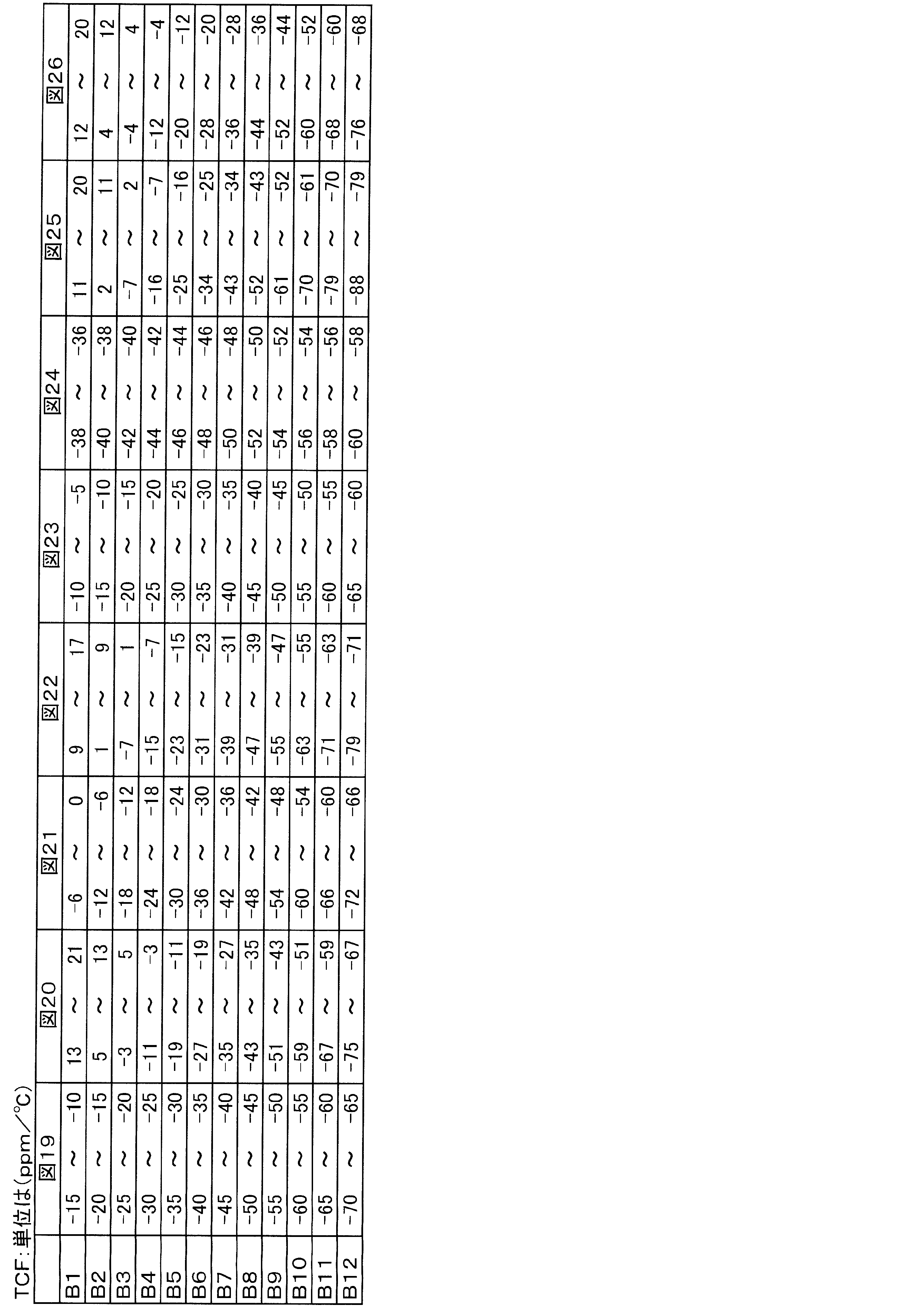
- FIGS. 11 to 18 show that ⁇ , ⁇ , and ⁇ in LiTaO 3 with Euler angles ( ⁇ , ⁇ , ⁇ ) when the thickness of the piezoelectric thin film 4 made of LiTaO 3 is 0.15 ⁇ , and the sound speed of each mode. shows TCF, the relationship between the power flow angle PFA and the electromechanical coupling coefficient k 2. That is, FIGS. 11 to 18 show the sound speed and Euler angle (U3-1, U2-1, U1-1, U2-2, U1-2, U3-2, U2-3, and U1-3 modes, respectively). It is a figure which shows the relationship with (theta) and (psi) in 0 degree, (theta), (psi).
- U3”, “U2”, and “U1” in U3-1, U2-1, U1-1, U2-2, etc. are the U3 mode in which the main displacement component is U3 and the main, respectively. It shows that the displacement component is the U2 mode of U2, and the main displacement component is the U1 mode of U1.
- ⁇ 1” in “U3-1” indicates a fundamental wave of the U3 mode
- ⁇ 2” in “U2-2” indicates a secondary mode of the U2 mode.
- a plate wave secondary mode mainly having a U1 component that is, a U1-2 mode is used. Therefore, it is a mode other than the U1-2 mode or a spurious mode.
- FIGS. 19 to 26 show the UCF, Euler angle (0 °), and the TCF in the U3-1, U2-1, U1-1, U2-2, U1-2, U3-2, U2-3 and U1-3 modes, respectively.
- ⁇ , ⁇ ) is a diagram showing the relationship between ⁇ and ⁇ .
- FIGS. 27 to 34 show the PFA and Euler angles for each of the U3-1, U2-1, U1-1, U2-2, U1-2, U3-2, U2-3, and U1-3 modes. It is a figure which shows the relationship with (theta) and (psi) of (0 degree, (theta), (psi)).
- regions B1 to B12 in FIGS. 19 to 26 indicate that the TCF is within the ranges shown in Table 2 below.
- regions C1 to C12 in FIGS. 27 to 34 indicate that the PFA values are within the ranges shown in Table 3 below.
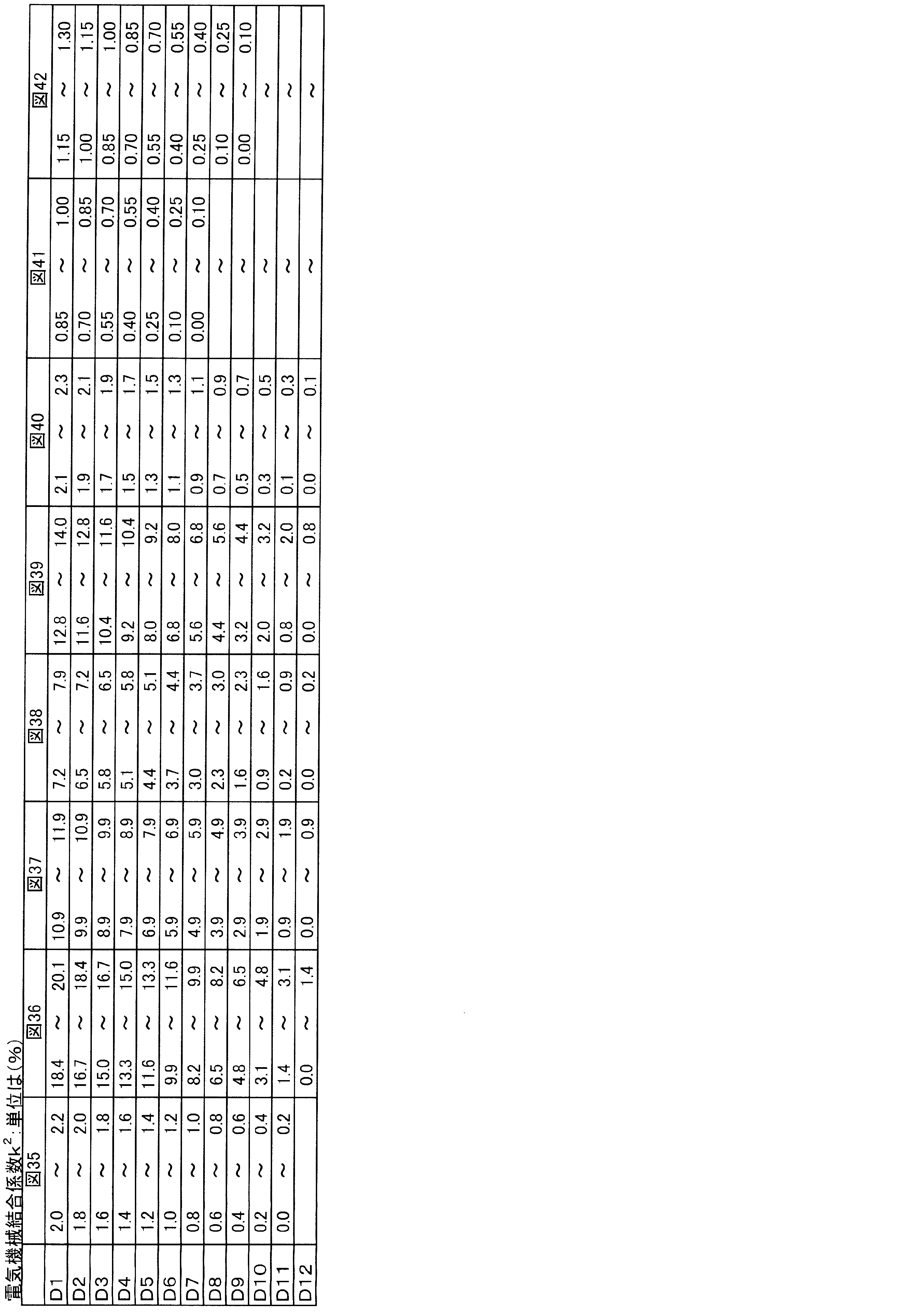
- Regions D1 ⁇ D12 in FIGS. 35 to 42 show that the electromechanical coupling coefficient k 2 is within the range shown in Table 4 below.
- the sound velocity of the U1-2 mode that is, the secondary mode of the plate wave mainly composed of the U1 component
- the sound speed is as high as 12750 m / sec or more. Therefore, it can be seen that higher sound speed can be achieved compared to the sound speed of 3000 to 4000 m / sec described in Patent Document 1. This is because the sound speed of the U1-2 mode is high.
- the absolute value of the power flow angle PFA can be reduced by selecting the Euler angles ⁇ and ⁇ as the power flow angle PFA. More specifically, in the Euler angles (0 °, ⁇ , ⁇ ), it can be seen that there is a region where the power flow angle can be made 2 ° or less by selecting ⁇ and ⁇ .
- the electromechanical coupling coefficient k 2 of each mode varies greatly depending on ⁇ and ⁇ of Euler angles (0 °, ⁇ , ⁇ ). Since the U1-2 mode is used, the other modes are spurious. Accordingly, the electromechanical coupling coefficient k 2 of the other modes is small desirably.
- the U2-1, U1-1, U2-2, and U3-2 modes have similar spurious effects because the sound speed is close to that of U1-2. coefficient k 2 is small is obtained.
- U2-3, modes U1-3 because the electromechanical coupling coefficient k 2 is very small, no problem.
- the electromechanical coupling coefficient k 2 of U3-1 mode is relatively large, since the sound velocity is slow, by limiting the thickness of the piezoelectric thin film, reducing the electromechanical coupling coefficient k 2, is a mode using U1 -2 mode can be separated. This will be clarified by explaining the propagation characteristics of each mode depending on the thickness of LiTaO 3 described later.
- FIG. 4 shows the results obtained by plotting the above range from FIG. 31 and FIGS. 35 to 42.
- 31 and FIGS. 35 to 42 show the results in the case of Euler angles (0 °, ⁇ , ⁇ ), but similar results are obtained as long as ⁇ is in the range of 0 ° to 2.5 °. was gotten.
- FIGS. 5 to 10 are also obtained in the same manner as in the case of FIG.
- the piezoelectric thin film is not mechanically constrained.
- the mode mainly composed of each displacement component is classified into a basic mode and a higher-order mode.
- the frequency temperature coefficient TCF was determined as follows.
- Electromechanical coupling coefficient k 2 (%): obtained by k 2 2 ⁇ (Vf ⁇ Vm) / Vm.
- the power flow angle is an angle representing a difference between the direction of the phase velocity of the elastic wave and the direction of the group velocity along which the energy of the elastic wave advances. If the power flow angle is large, the IDT electrode must be inclined to the power flow angle. Therefore, the electrode design becomes complicated. Also, loss due to angular deviation is likely to occur.
- TCF (Vm (30 ° C.) ⁇ Vm (25 ° C.) / Vm (25 ° C.) ⁇ ⁇ ) Vm (30 ° C.) represents Vm at 30 ° C., Vm (25 ° C.) represents Vm at 25 ° C., and ⁇ represents the linear expansion coefficient of the piezoelectric thin film in the elastic wave propagation angle direction.
- the Euler angles ( ⁇ , ⁇ , ⁇ ) of LiTaO 3 in the present invention include crystallographically equivalent Euler angles.
- LiTaO 3 is a crystal belonging to the trigonal 3m point group, and therefore the following equation holds.
- F is an acoustic wave characteristic such as sound velocity, electromechanical coupling coefficient k 2 , TCF, or PFA.
- PFA electromechanical coupling coefficient
- the sound speed in the U1-2 mode is very high, about 14000 m / sec, when the Euler angle ⁇ is in the range of 20 ° to 40 °, that is, 30 ° ⁇ 10 °. .
- FIG. 43 the sound speed in the U1-2 mode is very high, about 14000 m / sec, when the Euler angle ⁇ is in the range of 20 ° to 40 °, that is, 30 ° ⁇ 10 °. .
- TCF is ⁇ 25 to ⁇ 15 ppm / ° C., that is, the absolute value is 25 or less within the range of ⁇ of 30 ° ⁇ 10 °, and the absolute value of TCF is relatively small.
- the Euler angles ⁇ in a range of 30 ° ⁇ 10 ° the electromechanical coupling coefficient k 2 is seen to be very high as about 12% to 12.5%.
- the sound velocity in the U1-2 mode is 14070 m / sec
- the TCF is ⁇ 17.9 ppm / ° C.
- the electromechanical coupling coefficient k 2 is high at 12.2%.
- FIG. 58 shows the relationship between the normalized film thickness H / ⁇ of LiTaO 3 and the sound speed.
- the displacement distribution in the thickness direction in each mode is schematically shown on both sides of the graph showing the relationship between the sound speed and the normalized film thickness.
- the displacement in the figure is the absolute value of the magnitude, and the point where the displacement is zero is a node, indicating that the direction of displacement differs before and after this thickness.
- the U1-2 mode used in the present invention has a high sound velocity of 14070 m / sec at the Euler angles (0 °, 33 °, 0 °) as described above. And when using this mode, it turns out that it is an elastic wave which has U1 component as a main component, and also contains U2 component and U3 component. Further, since the main U1 component has one node in the thickness direction, it can be seen that it is a second-order higher-order mode.
- U1-2 mode corresponds to the mode A 1 in Non-Patent Document 1 described above. Also, when described for reference, U1-1 mode in FIG.
- Non-Patent Document 1 corresponds to the mode S 0 described in Non-Patent Document 1
- U3-1 mode corresponds to the mode A 0 in the non-patent document 1.
- the real number of the fundamental wave is represented as 0, and S 0 is represented as A 0.
- the fundamental wave is represented as a primary mode and is represented as U1-1 or U3-1. ing.
- Non-Patent Document 1 the secondary mode is expressed by degree 1 as A 1 , but in this specification, the secondary mode is expressed by “ ⁇ 2” as U1-2. is doing.
- FIGS. 46 to 48 the Euler angles (0 °, 33 °, 0 °) and the normalized thickness H / lambda of the LiTaO 3 film in LiTaO 3 of sonic, the electromechanical coupling factor k 2 and TCF Each relationship is shown.
- the sound velocity of the U1-2 mode to be used is 8400 m / sec or more and the electromechanical coupling coefficient k 2 is 5. It can be seen that it can be as high as 8% or more and that the absolute value of TCF can be 42 ppm / ° C. or less. Therefore, it is preferable that the standardized film thickness of the LiTaO 3 film is 0.3 or less.
- the sound speed of the U1-2 mode to be used is 8000 m / sec when the normalized film thickness is 0.3 or less. high.
- the U2-1 mode electric machine it can be seen that the coupling coefficient k 2 becomes as high as 4% or more.
- Euler angles (0 °, 0 °, 0 °) In can not be an electromechanical coupling coefficient k 2 of the spurious mode to be 2% or less.
- the sound velocity of the U1-2 mode used is as high as 8200 m / sec or more.
- the electromechanical coupling coefficient k 2 of U1-2 mode is as high as 5.8% or more, of the other mode in which a spurious electromechanical coupling coefficient k 2 is as small as 2% or less.
- the absolute value of the TCF in the U1-2 mode is as small as 52 ppm / ° C. or less.
- the standardized film thickness of the LiTaO 3 film is set to 0.3 or less so that the U1-2 mode is achieved. It can be seen that the speed of sound can be increased to 8500 m / sec or more, the electromechanical coupling coefficient k 2 can be 5% or more, and the absolute value of TCF can be less than 35 ppm / ° C.
- the electromechanical coupling coefficient k 2 may electromechanical coupling coefficient k 2 of these other modes than 2% I understand that. In the U3-1 mode, as described above, it can be easily removed by a filter using the difference in sound speed.
- FIG. 59 is a diagram showing the relationship between the normalized film thickness of LiTaO 3 with Euler angles (0 °, 33 °, 0 °) and the frequency-temperature characteristic TCF.
- the thickness of LiTaO 3 is desirably in the range of 0.08 to 0.10 in terms of the normalized film thickness H / ⁇ in order to further improve the temperature characteristics.
- V S 2 indicates the speed of sound in the short-circuit state corresponding to the resonance point
- V O 2 indicates the speed of sound in the open state corresponding to the anti-resonance point
- TCV S 2 indicates a TCV in a short-circuit state corresponding to a resonance point
- TCV O 2 indicates a TCV in an open state corresponding to an anti-resonance point.
- the electromechanical coupling coefficient k 2 can be increased to 6% or more, and V S 2 and V S Any O 2 can be increased to 11400 m / sec or more.
- the absolute value of the TCV S 2 and TCV O 2, respectively may be a 70 ppm / ° C. or less and 118 ppm / ° C. or less.
- FIGS. 60 to 62 are the same as FIGS. 60 to 62 except that the Euler angles are (0 °, 15 °, 0 °), and the electromechanical coupling coefficient k 2 at 25 ° C.
- FIG. 66 to FIG. 68 show the relationship between the film thickness and the Al film thickness.
- FIG. 66 to FIG. 68 are the same as FIG. 60 to FIG. 62 except that the Euler angles are changed to (0 °, 55 °, 0 °). The results obtained in the same manner are shown.
- the normalized film thickness of the Al film is desirably 0.08 or less even when the Euler angle is changed.
- the power flow angle PFA was 0 ° in any of the examples shown in Table 5.
- Table 5 when any of Al, Ti, Fe, Cu, Mo, Ag, Ta, Au, W, and Pt is used, U2-1, U1-2, U2-2, U3- electromechanical coupling factor of 1 modes k 2 it can be seen that the 2% and lower. Therefore, the electrode material is not particularly limited, and it can be seen that the use of any of the above metals can effectively suppress the influence of other modes that become spurious and can reduce the absolute value of PFA.
- FIG. 2 is a schematic front cross-sectional view showing a main part of an elastic wave device according to the second embodiment of the present invention.
- FIG. 2 is a diagram corresponding to the schematic cross-sectional view of FIG. 1A shown in the first embodiment.
- the dielectric film 3 is formed on the upper surface of the piezoelectric thin film 4. That is, the dielectric film 3 is formed so as to cover the IDT electrode 5.
- the dielectric film 3 may be formed on the upper surface of the piezoelectric thin film 4.
- FIGS. 3A and 3B are views corresponding to FIG. 1A shown for the first embodiment.
- the dielectric film 3 is formed on the lower surface side of the piezoelectric thin film 4.
- the IDT electrode 5 may be formed on the lower surface of the piezoelectric thin film 4 as in the elastic wave device 31 ⁇ / b> A of the modified example of FIG. That is, the IDT electrode 5 is formed so as to face the space formed by the recess 2a. Thus, the IDT electrode 5 may be formed on the lower surface of the piezoelectric thin film 4.
- the dielectric film 3 is laminated on the piezoelectric thin film 4.
- the dielectric film 3 is formed on the upper surface or the lower surface of the piezoelectric thin film 4, but may be formed on both the upper surface and the lower surface. Furthermore, in the present invention, the dielectric film 3 is not essential, and the dielectric film 3 may not be provided.
- the dielectric film 3 can be formed of an appropriate dielectric material such as silicon oxide, silicon nitride, or aluminum nitride.
- the frequency can be adjusted by cutting the dielectric film 3 by ion milling or the like.
- the frequency adjustment is further performed. It can be done more easily.
- the absolute value of the frequency temperature coefficient TCF can be reduced. This will be described with reference to FIG.
- FIG. 69 is a diagram showing the relationship between the normalized film thickness of the piezoelectric thin film 4 and the frequency temperature coefficient TCF in various acoustic wave devices configured according to the present invention.
- a LiTaO 3 thin film having Euler angles (0 °, 33 °, 0 °) was used as the piezoelectric thin film 4.
- the IDT electrode 5 was formed by sequentially forming a 20 nm Ti film and a 200 nm thick Al film.
- the wavelength ⁇ of the propagating elastic wave is 3.5 ⁇ m.
- the film thickness of the dielectric film 3 was 175 nm. Note that the Ti film plays a role of adhering the Al film to LiTaO 3 .
- the acoustic thin film device was manufactured by varying the normalized film thickness of the piezoelectric thin film 4 made of LiTaO 3 , and the frequency temperature coefficient TCF was measured.
- the prepared samples are as follows.
- Example 1 An elastic wave device similar to that of the first embodiment.
- Example 2 According to the third embodiment shown in FIG. 3A, an SiO 2 film having a thickness of 0.05 ⁇ was formed as the dielectric film 3.
- Example 3 Similar to the third embodiment shown in FIG. 3A, except that a SiN film having a thickness of 0.05 ⁇ was formed as the dielectric film 3.
- Example 4 Similar to the third embodiment shown in FIG. 3A, except that an AlN film having a thickness of 0.05 ⁇ was formed as the dielectric film 3.
- an acoustic wave device was manufactured and its frequency temperature coefficient TCF was measured.
- the piezoelectric thin film 4 a LiTaO 3 thin film having Euler angles (0 °, 33 °, 0 °) and a thickness of 0.18 ⁇ was used.
- the propagating elastic wave has a wavelength ⁇ of 3.5 ⁇ m, and the IDT electrode 5 was formed by sequentially forming a 20 nm Ti film, a 35 nm Pt, and a 35 nm thick Al film. Further, a structure in which the dielectric film 3 was not formed on the IDT and a structure in which the dielectric film 3 was formed were produced.
- the dielectric film 3 is made of SiO 2 and the film thickness is 105 nm.
- the TCF of the structure without the dielectric film 3 was ⁇ 8.6 [ppm / ° C.], and the TCF of the structure with the dielectric film 3 formed was ⁇ 1.4 [ppm / ° C.]. It can be seen that even when a dielectric is formed on the IDT, the absolute value of TCF can be reduced.
- the first-order temperature coefficient (1 / x) ( ⁇ x / ⁇ T) of the elastic constant Cij of LiTaO 3 is a negative value.
- the first-order temperature coefficient of the elastic constant of SiO 2 is a positive value. Therefore, by laminating SiO 2 , the plus and minus of the temperature coefficient of the elastic constant cancel each other, and as a result, the absolute value of TCF can be reduced.
- the linear expansion coefficient of dielectrics such as SiO 2 , SiN, and AlN is smaller than that of LiTaO 3 . Further, the film thickness of the piezoelectric thin film 4 made of LiTaO 3 is very small.
- the linear expansion coefficient of LiTaO 3 is 16 ppm / ° C.
- the linear expansion coefficient of SiO 2 is 0.6 ppm / ° C.
- the linear expansion coefficient of SiN is 3 ppm / ° C.
- the linear expansion coefficient of AlN is about 4 to 5 ppm / ° C.
- the dielectric film 3 is formed on the lower surface of the piezoelectric thin film 4, and the IDT electrode 5 is formed on the upper surface.
- the dielectric film 3 is preferably formed so as to apply a tensile stress to the piezoelectric thin film 4 made of LiTaO 3 .
- the upper surface side from which the IDT electrode 5 is projected is convex. In this case, it is possible to reduce the possibility that the portion where the plate wave located on the recess 2a propagates contacts the support layer 2 below the recess 2a or contacts other portions such as an adhesive layer. it can. Therefore, the plate wave propagates stably.
- the portion where the plate wave propagates contacts a part of the support layer 2 below the concave portion 2a. Or may come into contact with an adhesive layer (not shown). In addition, there is a possibility that a portion where a plate wave floating in the air propagates is brought into contact with the support layer 2 due to the electrostatic force.
- the tensile stress is a stress in a direction in which the stress caused by the dielectric film 3 acts to compress the piezoelectric thin film 4 made of LiTaO 3 at the interface between the piezoelectric thin film 4 made of LiTaO 3 and the dielectric film 3. .
- the stress applied to the LiTaO 3 of the dielectric film 3 can be easily adjusted in a wide range from compressive stress to tensile stress by adjusting the pressure during film formation. it can. Therefore, it is preferable to use an AlN film as the dielectric film 3.
- LiTaO 3 is a ferroelectric material, it has pyroelectric properties. Therefore, when a temperature change or a pressure change is given, there is a possibility that pyroelectric charges are generated on the surface of the piezoelectric thin film 4. It is desirable that the piezoelectric thin film 4 has a certain degree of conductivity so that the IDT electrode 5 is not destroyed by the pyroelectric charge. When the insulation resistance R of the IDT electrode is 1 M ⁇ or less, the pyroelectric charge on the piezoelectric thin film 4 is effectively neutralized, and the destruction of the IDT electrode 5 can be suppressed.
- the insulation resistance of the IDT electrode is smaller than 50 times the terminal impedance of the electric circuit to which the acoustic wave device 1 is connected, vibration energy is likely to leak through the piezoelectric thin film 4 made of LiTaO 3 . Therefore, it is desirable that the insulation resistance is greater than 50 times the termination impedance.
- the thickness of the piezoelectric thin film 4 made of LiTaO 3 is not particularly limited. However, when the thickness of the piezoelectric thin film 4 is 50 nm or less, the strength as a hollow structure is weakened, and there is a problem in practical reliability. Therefore, the thickness of the piezoelectric thin film made of LiTaO 3 is desirably 50 nm or more. The upper limit of the piezoelectric thin film 4 is desirably 0.3 ⁇ or less in order to sufficiently increase the sound speed of the second-order mode of the plate wave having the U1 component as a main component of displacement.
- the piezoelectric thin film 4 and the IDT electrode 5 are arranged on the recess 2 a, and one elastic wave resonator in which reflectors are arranged on the left and right sides of the IDT electrode 5 is configured.
- a plurality of elastic wave devices 1 and 1A may be combined.
- a plurality of recesses 2a are formed on the support layer 2, and an acoustic wave element such as an acoustic wave resonator is formed at the position where each recess 2a is provided, as in the present embodiment. Is desirable.
- a plurality of acoustic wave resonators may be used as in this embodiment, or a filter may be configured by combining a plurality of acoustic wave elements such as a resonator type filter. . Furthermore, a duplexer or the like may be configured by combining these acoustic wave elements and other elements.
- a ladder filter, a lattice filter, or the like can be given as a filter formed by combining a plurality of acoustic wave resonators as described above.
- the 71 may be different from the propagation azimuth ⁇ of the elastic wave device 1A. Since the plate wave is a non-leakage type propagation mode, it does not attenuate even when the propagation direction ⁇ is changed. Accordingly, the Q of the acoustic wave resonator is not deteriorated.
- the propagation direction of at least one acoustic wave element may be different from the propagation direction of at least one of the remaining acoustic wave elements.
- each optimal electromechanical coupling coefficient k 2 can be easily set. Therefore, the degree of freedom in designing a filter or the like can be greatly increased.
- the method for manufacturing the acoustic wave device according to the present invention is not particularly limited, but an example thereof will be described with reference to FIG.
- 70 (a) to (i) are schematic front cross-sectional views showing an example of the method for manufacturing the acoustic wave device of still another first embodiment of the present invention.
- a LiTaO 3 wafer 41 is prepared.
- H + ions accelerated at 100 keV are implanted into the upper surface of the LiTaO 3 wafer 41 at a concentration of 8 ⁇ 10 16 at / cm 2 .
- the hydrogen ion concentration in the LiTaO 3 wafer 41 has a distribution in the thickness direction.
- a portion having the highest hydrogen ion concentration is indicated by a broken line as a hydrogen ion high concentration implantation portion 41a.
- the depth at which the hydrogen ion high concentration implantation portion 41 a is formed is a certain depth from the upper surface of the LiTaO 3 wafer 41.
- the depth of the hydrogen ion high concentration implantation portion 41a is set slightly deeper than the thickness of the piezoelectric thin film 4 to be finally formed.
- the piezoelectric thin film 4A and the remaining LiTaO 3 wafer portion 41b are separated by heating. At least a part from the hydrogen ion high concentration implantation portion 41a to the wafer surface on the hydrogen ion implantation side is used as a piezoelectric thin film. Therefore, by performing such a separation experiment in advance, the depth of the hydrogen ion high concentration implantation portion 41a can be controlled according to the thickness of the piezoelectric thin film 4 to be finally formed. Alternatively, the position of the hydrogen ion high concentration implantation portion 41a may be confirmed by measuring the hydrogen ion concentration inside the LiTaO 3 wafer 41 after hydrogen ion implantation.
- the depth of the hydrogen ion high concentration implantation portion 41a is a little deeper than the thickness of the piezoelectric thin film 4 to be finally formed. Therefore, in the present embodiment, as described above, the depth of the hydrogen ion high concentration implantation portion 41 a is slightly deeper than the thickness of the piezoelectric thin film 4. In this case, after the piezoelectric recovery step, a processing step is performed to reduce the thickness by polishing or the like from the hydrogen ion high concentration implanted portion 41a side. Thereby, the piezoelectric thin film 4 having excellent piezoelectricity and uniform piezoelectricity can be obtained.
- Cu is formed on the surface of the LiTaO 3 wafer on the piezoelectric thin film 4A side as a sacrificial layer 42 with a thickness of 2 ⁇ m by vapor deposition.
- the sacrificial layer 42 can be formed of an appropriate material that disappears by etching, for example.
- SiO 2 is formed as the support layer 2 by about 5 ⁇ m by sputtering.
- a LiTaO 3 wafer having the same Euler angle as the piezoelectric layer is bonded to the lower surface of the support layer 2 as the support wafer 2A.
- the support wafer 2A is not limited to the LiTaO 3 wafer, but may be, for example, a dielectric ceramic wafer or a high resistance Si wafer, or may not be formed.
- the piezoelectric thin film 4A and the remaining portion 41b of the LiTaO 3 wafer 41 are separated from each other at the hydrogen ion high concentration implantation portion 41a. In the hydrogen ion high concentration implantation portion 41a, separation can be easily performed by heating.
- the thin piezoelectric thin film 4A having an arbitrary Euler angle can be sliced from the wafer on the support layer 2, and can be formed with a uniform thickness.
- the surface of the separated piezoelectric thin film 4A is polished by 0.1 ⁇ m, and the piezoelectricity is recovered by heating. Thereby, the final piezoelectric thin film 4 is obtained.
- the IDT electrode 5 is formed on the piezoelectric thin film 4 as shown in FIG.
- the piezoelectric thin film 4A is patterned as shown in FIG. 70 (h) to form openings 6 and 7 that expose a part of the sacrificial layer.
- the sacrificial layer 42 is removed by etching through the opening. In this way, an elastic wave device similar to that of the first embodiment can be obtained.
- the dielectric film 3 is formed on the surface of the piezoelectric thin film 4A after ion implantation, and then the sacrificial layer is formed.
- An elastic wave device similar to that of the third embodiment shown in 3 (a) can be obtained.
Landscapes
- Physics & Mathematics (AREA)
- Acoustics & Sound (AREA)
- Engineering & Computer Science (AREA)
- Manufacturing & Machinery (AREA)
- Chemical & Material Sciences (AREA)
- Materials Engineering (AREA)
- Surface Acoustic Wave Elements And Circuit Networks Thereof (AREA)
Abstract
高音速であり、使用するモード以外の他のモードによるスプリアスの影響を抑制することができる、板波を利用した弾性波装置を提供する。 上面に開いた凹部2aまたは貫通孔が形成されている支持層2と、前記支持層2の前記凹部2aまたは貫通孔上に至るように前記支持層2上に形成された圧電薄膜4と、該圧電薄膜4の前記凹部2aまたは貫通孔上に至っている領域において、前記圧電薄膜4の上面及び下面の内の少なくとも一方の面に形成されたIDT電極5とを備え、U1成分を主成分とする板波の二次モードを用いており、前記圧電薄膜4がLiTaO3からなり、該LiTaO3のオイラー角(φ,θ,ψ)が、図4~図10の実線で囲んである領域R1~R7のいずれの範囲内にある、弾性波装置1。
Description
本発明は、圧電薄膜を用いた弾性波装置及びその製造方法に関し、より詳細には、ラム波と称されている板波の高次モードを用いた弾性波装置及びその製造方法に関する。
近年、通信機器等の高周波化に伴って圧電薄膜を用いた弾性波装置が提案されている。高周波化を進めるためには、圧電基板における弾性波の音速が高いことが必要である。そのため、音速の高い、板波を用いた弾性波装置が注目されている。
板波とは、2つの自由境界面に挟まれた媒質中を伝搬する弾性波である。板波としては、下記の非特許文献1に記載のように、SH波やラム波が知られている。非特許文献1に記載のように、SH波は、U2成分主体の波であり、ラム波はU1成分及びU3成分を主体とする。もっとも、圧電単結晶は異方性結晶である。そのため、圧電単結晶を伝搬する板波は、SH波であっても、若干のU1成分やU3成分を含む。同様に、ラム波の場合には、U1成分またはU3成分を主体とするが、若干のU2成分を含む。
なお、板波を励振した場合、いずれのモードでもU1成分、U2成分及びU3成分が伝搬するが、主体となる成分の変位が厚み方向に複数の節を持つ高次モードもそれぞれ伝搬する。節の無い最低次のモードを基本モードとすると、高次モードは次数の低いものから2次モード、3次モード、・・と区別できる。
他方、下記の特許文献1には、圧電薄膜を用いており、かつラム波を利用した弾性波装置が開示されている。特許文献1に記載の実施例では、圧電薄膜がLiTaO3からなり、該LiTaO3のオイラー角は(0°,126°±20°,0°)とされている。ここでは、伝搬する板波の音速は3300m/秒~4100m/秒程度であるとされている。
水谷,戸田:"回転YカットX伝搬LiNbO3平板におけるラム波伝搬特性の解析",信学論(A),J68-A,5,pp.496-503(1985-05)
前述のように、高周波化を図るには、弾性波の音速が高いことが強く求められる。特許文献1に記載の板波を利用した弾性波装置では、音速は3300~4100m/秒程度であり、音速が十分に高くない。このため、高周波帯である4GHz付近の帯域で使用する弾性波装置を構成した場合、IDT電極の電極指幅を0.2μm程度としなければならなかった。従って、IDT電極の形成に際し、非常に高い加工精度が要求されるという問題があった。また、電極指幅が非常に狭いため、配線抵抗が劣化したり、耐電力性が低下したりするという問題もあった。
本発明の目的は、板波を利用しており、より高音速であり、使用するモード以外のモードによるスプリアスの影響が小さい弾性波装置を提供することにある。
本発明に係る弾性波装置は、上面に開いた凹部または貫通孔を有する支持層と、支持層の凹部または貫通孔上に位置する部分を有するように、支持層上に形成された圧電薄膜と、圧電薄膜の前記凹部または貫通孔上に至っている領域において、圧電薄膜の上面及び下面の内の少なくとも一方の面に形成されたIDT電極とを備える。本発明の弾性波装置は、U1成分を変位の主成分とする板波の二次モードを用いている。本発明では、圧電薄膜は、LiTaO3からなり、そのオイラー角(φ,θ,ψ)が、添付の図4~図10において実線で囲んである領域R1~R7の範囲内にある。
本発明に係る弾性波装置のある特定の局面では、IDT電極が、AlもしくはAlを主成分とする合金からなり、かつ膜厚をHとしたときに、H≦0.08λとされている。なお、λは、利用する板波の二次モードの波長を示す。IDT電極がAlもしくはAlを主成分とする合金からなる場合には、電極の電気抵抗を低めることができる。従って、弾性波装置の共振特性やフィルタ特性を高めることができる。また、膜厚Hが0.08λ以下の場合には、使用する二次モードの電気機械結合係数k2を6%以上とより一層高くすることができる。
本発明に係る弾性波装置の他の特定の局面では、圧電薄膜の上面及び下面の内の少なくとも一方の面に積層された誘電体膜をさらに備える。この誘電体膜の線膨張係数は、LiTaO3の線膨張係数よりも小さい。この場合には、弾性波装置の温度特性を改善することができる。
特に、上記誘電体膜としては、酸化ケイ素が好適に用いられ、その場合には、周波数温度係数TCFの絶対値を小さくすることができる。従って、温度特性をより効果的に改善することができる。
本発明に係る弾性波装置のさらに他の特定の局面では、前記圧電薄膜の上面にIDT電極が形成されており、圧電薄膜の下面に誘電体膜が形成されている。そして、誘電体膜は、LiTaO3からなる圧電薄膜に対して、引っ張り方向の応力を与えるように構成されている。この場合には、誘電体膜が圧電薄膜に引っ張り方向の応力を与えるので、IDT電極が形成されている面側が凸状となる。それによって、板波の二次モードの伝搬性が阻害され難い。
本発明に係る弾性波装置のさらに別の特定の局面では、IDT電極間の電気抵抗が弾性波装置を接続する電気回路の終端インピーダンスの50倍以上であり、かつ1MΩ以下とされている。この場合には、共振特性やフィルタ特性などの電気的特性の劣化を抑制でき、さらに焦電破壊を効果的に抑制することができる。
本発明に係る弾性波装置のさらに別の特定の局面では、上記圧電薄膜の厚みが50nm以上、0.3λ以下の範囲とされている。圧電薄膜の厚みを50nm以上とすることにより、圧電薄膜を安定に形成することができる。また、0.3λ以下の場合には、U1成分を変位の主成分とする板波の二次モードの音速を十分高くすることができる。
本発明に係る弾性波装置では、本発明の弾性波装置が複数組み合わされていてもよい。好ましくは、少なくとも1つの弾性波装置における伝搬方位ψが、他の少なくとも1つの弾性波装置の伝搬方位ψと異ならされる。この場合には、少なくとも1つの弾性波素子における電気機械結合係数k2を独立に設定することができる。従って、複数の弾性波装置を組み合わせた弾性波装置の設計の自由度を高めることができる。
本発明に係る弾性波装置の製造方法は、LiTaO3基板の表面からイオンを注入し、イオン注入部分をLiTaO3基板の片面側に形成する工程と、前記イオン注入した側の面の一部に犠牲層を形成する工程と、前記イオン注入した側の面及び前記犠牲層を覆うように絶縁体を形成して支持層とする工程と、加熱により、前記LiTaO3基板を前記イオン注入部分で分離し、LiTaO3基板から分離された圧電薄膜構造体を形成する工程と、前記犠牲層を消失させて、前記圧電薄膜の下方に前記支持層の凹部を形成する工程と、前記圧電薄膜の上面または下面の内少なくとも一方の面にIDT電極を形成する工程とを備える。
本発明に係る弾性波装置によれば、圧電薄膜の下方に凹部または貫通孔由来の空間が形成されている構造の弾性波装置において、LiTaO3からなる圧電薄膜のオイラー角が上記特定の範囲内とされているため、U1成分を変位の主成分とする板波の二次モードを効率良く伝搬させることができる。このU1成分を変位の主成分とする板波の二次モードの伝搬速度は、7000m/秒以上と高い。そのため、従来の弾性波装置に比べて、小型化及び高周波化を容易に図ることができる。
また、主モードである上記二次モードのパワーフロー角PFAが小さいため弾性波装置の電極設計を容易に行うことができる。さらに主モード以外のスプリアスとなる伝搬モードの電気機械結合係数k2を小さくし得るので、共振特性やフィルタ特性上にスプリアスが生じ難い。
以下、図面を参照しつつ、本発明の具体的な実施形態を説明することにより、本発明を明らかにする。
図1(a)は、本発明の第1の実施形態にかかる弾性波装置の要部を示す模式的正面断面図であり(b)中のZ-Z線に沿う部分を示し、(b)はその平面図である。
弾性波装置1は、支持層2を有する。支持層2は、上面に開いた凹部2aを有する。凹部2a上に一部が位置するように、圧電薄膜4が積層されている。本実施形態では、圧電薄膜4はLiTaO3からなる。圧電薄膜4上に、IDT電極5が形成されている。
図1(b)に示すように、本実施形態では、圧電薄膜4上に上記IDT電極5を有する弾性波共振子が構成されている。なお、上記凹部2aは、図1(b)の破線で示す平面形状を有する。また、図1(b)の開口部6,7は、図1(a)に示すように、圧電薄膜4の一部を切り欠くことにより形成されている。従って、開口部6,7に挟まれた圧電薄膜部分の下方には、凹部2aに由来する空間が形成されている。本発明の弾性波装置1は、このような圧電薄膜4の下方に空間を有する形式の弾性波装置である。
上記支持層2は、酸化ケイ素や窒化アルミニウム、アルミナなどの適宜の誘電体あるいは高抵抗Siウエハにより形成することができる。LiTaO3は負の周波数温度係数TCFを有する。
IDT電極5は、Al、Cu、Ag、Pt、Ti、Fe、Mo、Ta、W、Cr、Niなどの適宜の金属もしくは合金により形成することができる。本実施形態では、IDT電極5はAlからなる。IDT電極5は好ましくはAlもしくはAlを主体とする合金からなることが望ましい。それによって、IDT電極5における電極抵抗を小さくすることができ、弾性波装置1の電気的特性を高めることができる。ただし、後述するように、AlからなるIDT電極5の膜厚を、0.08λ以下とすることが望ましく、それによって、板波の二次モードの電気機械結合係数k2を6%以上と高くすることができる。
本実施形態の弾性波装置1の特徴は、上記圧電薄膜4が、特定のオイラー角範囲のLiTaO3からなることにある。それによって、板波のU1成分を主体とする二次モードを効率よく励振させることができ、かつ他のモードによるスプリアスの影響を抑制し得ることにある。これを、以下において詳述する。
本実施形態の弾性波装置1では、LiTaO3のオイラー角(φ,θ,ψ)が、図4~図10に実線で囲んである領域R1~R7の範囲内にある。なお、R1を代表して説明すると、図4においては、実線で囲んである複数の部分が示されているが、領域R1はこの複数の実線で囲んである部分からなるものとする。言い換えれば、実線で囲んである複数の部分が分散されているが、領域R1はこれらの複数の部分の合計をいうものとする。領域R2~R7も同様である。
オイラー角(φ,θ,ψ)が上記領域R1~R7内にある場合、利用するモードすなわちU1成分を主要成分とする板波の二次モードのパワーフロー角PFAの絶対値を2°以下とすることができ、かつスプリアスとなる他のモードの電気機械結合係数k2を2%以下とすることができる。これを領域R1を代表例として、図11~図42を参照して説明する。図11~図42の結果は、LiTaO3からなる圧電薄膜4の厚みを0.15λとした場合のオイラー角(φ,θ,ψ)のLiTaO3におけるφ,θ及びψと、各モードの音速、TCF、パワーフロー角PFA及び電気機械結合係数k2との関係を示す。すなわち、図11~図18は、それぞれ、U3-1、U2-1、U1-1、U2-2、U1-2、U3-2、U2-3及びU1-3モードの音速と、オイラー角(0°,θ,ψ)におけるθ及びψとの関係を示す図である。ここで、U3-1、U2-1、U1-1、U2-2、等における「U3」、「U2」及び「U1」は、それぞれ、主体となる変位成分がU3のU3モード、主体となる変位成分がU2のU2モード、主体となる変位成分がU1のU1モードであることを示す。また、「U3-1」における「-1」は、U3モードの基本波であることを示し、「U2-2」における「-2」は、U2モードの二次モードであることを示す。
本実施形態の弾性波装置では、U1成分を主体とする板波の二次モードすなわちU1-2モードを利用する。従って、U1-2モード以外の他のモードかスプリアスとなるモードである。
各モードの詳細については、後述する。
図11~図18における領域A1~A12は、音速が下記の表1の範囲内であることを示す。

図19~図26は、それぞれ、U3-1、U2-1、U1-1、U2-2、U1-2、U3-2、U2-3及びU1-3モードのTCFと、オイラー角(0°,θ,ψ)のθ及びψとの関係を示す図である。同様に、図27~図34は、U3-1、U2-1、U1-1、U2-2、U1-2、U3-2、U2-3及びU1-3の各モードのPFAと、オイラー角(0°,θ,ψ)のθ及びψとの関係を示す図である。
図35~図42は、U3-1、U2-1、U1-1、U2-2、U1-2、U3-2、U2-3及びU1-3の各モードと、電気機械結合係数k2と、オイラー角(0°,θ,ψ)のθ及びψとの関係を示す図である。
また、図19~図26の領域B1~B12は、TCFが下記の表2に示す各範囲内にあることを示す。
同様に、図27~図34の領域C1~C12は、PFAの値が下記の表3に示す各範囲内にあることを示す。
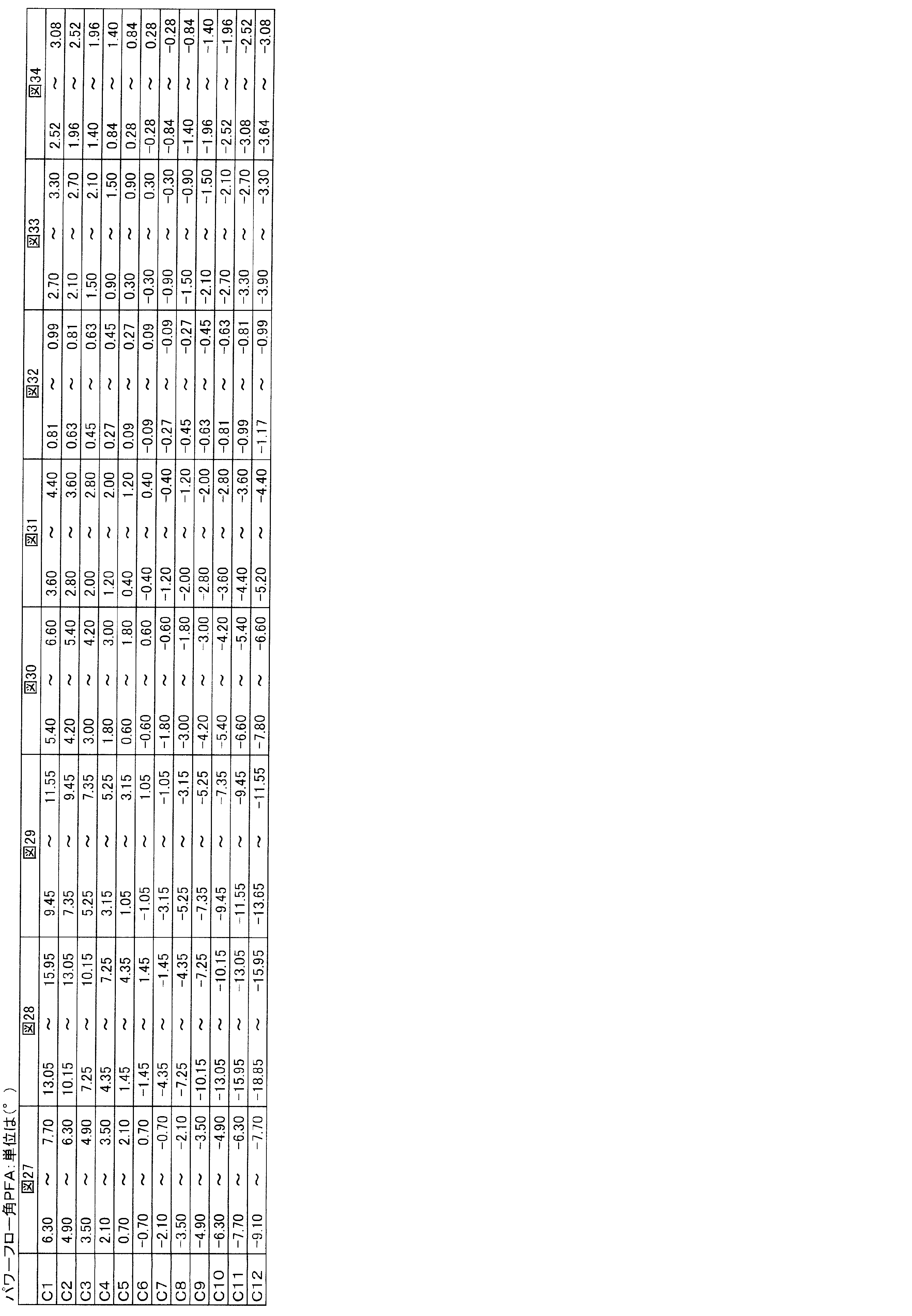
図35~図42における領域D1~D12は、電気機械結合係数k2が下記の表4に示す各範囲内にあることを示す。
まず、図15から明らかなように、U1-2モードすなわちU1成分が主体の板波の二次モードの音速は、オイラー角(0°,θ,ψ)において、θ及びψが広い範囲にわたり、その音速は12750m/秒以上と早いことがわかる。従って、特許文献1に記載の3000~4000m/秒の音速に比べ、高音速化を図り得ることがわかる。これは、U1-2モードの音速が高いことによる。
そして、図31から明らかなように、U1-2モードを利用した場合、パワーフロー角PFAをオイラー角のθ及びψを選択することによりパワーフロー角PFAの絶対値を小さくし得ることがわかる。より具体的には、オイラー角(0°,θ,ψ)において、θ及びψを選択することにより、パワーフロー角を2°以下とし得る領域の存在することがわかる。他方、図35~図42から、上記各モードの電気機械結合係数k2がオイラー角(0°,θ,ψ)のθ及びψにより大きく変化することがわかる。U1-2モードを利用するため、これ以外の他のモードはスプリアスとなる。従って、他のモードの電気機械結合係数k2は小さいことが望ましい。
なお、各モードのうち、U2-1、U1-1、U2-2及びU3-2の各モードはU1-2と音速が近いため、スプリアスとしての影響が大きく、従って、これらのモードの電気機械結合係数k2が小さいことが求められる。他方、U2-3、U1-3の各モードは、電気機械結合係数k2が非常に小さいため、問題とはならない。また、U3-1モードの電気機械結合係数k2は比較的大きいが、音速が遅いため、圧電薄膜の厚みを限定することにより、電気機械結合係数k2を小さくし、利用するモードであるU1-2モードから隔てることができる。この点については、後述のLiTaO3の厚みによる各モードの伝搬特性を説明することにより、明らかにする。
図4の領域R1は、U1-2モードを利用した場合のパワーフロー角PFAの絶対値が2°以下であり、かつU1-2以外の他のモードの電気機械結合係数k2が2%以下である範囲を図31と図35~図42に基づき求めたものである。すなわち、図31と図35~図42とから上記範囲を求め、プロットした結果が、図4である。なお、上記図31及び図35~図42は、オイラー角(0°,θ,ψ)の場合の結果であるが、φが0°~2.5°の範囲内であれば、同様の結果が得られた。
図5~図10の結果も、上記図4の場合と同様にして求めた結果である。
従って、図4~図10から明らかなように、LiTaO3のオイラー角を図4~図10のハッチングを付して示した領域R1~R7の範囲内とすれば、利用するモードであるU1-2モードのパワーフロー角の絶対値を2°以下とし、かつスプリアスとなる他のモードの電気機械結合係数k2を2%以下と小さくし得ることがわかる。また、図38から明らかなように、利用するモードの電気機械結合係数k2を5%以上と充分に大きくし得ることがわかる。それによって、共振特性やフィルタ特性におけるスプリアスの特性を図ることができ、かつ広い帯域の共振子やフィルタを提供し得ることがわかる。また、高音速化を図り得るので、弾性波装置1の高周波化を図ることができる。
上記図4~図10の結果をまとめるにあたって、前提条件は以下の通りとした。
圧電薄膜は機械的に拘束されてない。各変位成分を主体とするモードを基本モード及び高次モードに分類し、各モードについて、(1)音速V、(2)電気機械結合係数k2、(3)パワーフロー角PFA及び(4)周波数温度係数TCFを以下のようにして求めた。
(1)音速V:圧電薄膜の一方面を電気的に短絡し、残りの面を電気的に開放した短絡状態の音速Vmと、圧電薄膜の両面が電気的に開放されている開放状態の音速Vfとを求めた。
(2)電気機械結合係数k2(%):k2=2×(Vf-Vm)/Vmにより求めた。
(3)パワーフロー角PFA(°):PFA=tan-1{(Vm(ψ+0.5)-Vm(ψ-0.5))/Vm(ψ)}
なお、パワーフロー角は、弾性波の位相速度の方向と、弾性波のエネルギーが進む群速度の方向との差を表わす角度である。パワーフロー角が大きいと、IDT電極をパワーフロー角に合わせて傾斜させて配置しなければならない。従って、電極設計が煩雑となる。また、角度ずれによる損失が発生しやすくなる。
(4)周波数温度係数TCF(ppm/℃):TCF=(Vm(30℃)-Vm(25℃)/Vm(25℃)-α)で求めた。なお、Vm(30℃)は、30℃におけるVmを、Vm(25℃)は25℃におけるVmを示し、αは弾性波伝搬角方向における圧電薄膜の線膨張係数を示す。
なお、本発明におけるLiTaO3のオイラー角(φ,θ,ψ)は、結晶学的に等価なオイラー角をも含む。例えば、日本音響学会誌(36巻第3号、1984年、第140~145頁)によれば、LiTaO3は、三方晶系3m点群に属する結晶であるので、以下の式が成り立つ。
F(φ、θ、ψ)=F(60°+φ,-θ,ψ)=F(60°-φ,-θ,180°-ψ)=F(φ,180°+θ,180°-ψ)=F(φ,θ,180°+ψ)
ここで、Fは、音速、電気機械結合係数k2、TCF又はPFAなどの弾性波特性である。PFAは、伝搬方向を正負反転した場合、符号は変わるが絶対量は等しい。従って、PFAの絶対値を問題とすればよい。
〔好ましい実施例〕
次に、本発明の好ましい実施例として、オイラー角(0°,θ,0°)のLiTaO3において、オイラー角のθが33°付近の構造の結果を図43~図45及び図58を参照してより詳細に説明する。
次に、本発明の好ましい実施例として、オイラー角(0°,θ,0°)のLiTaO3において、オイラー角のθが33°付近の構造の結果を図43~図45及び図58を参照してより詳細に説明する。
図43~図45は、オイラー角(0°,θ,0°)のθが30°付近の範囲にある場合のオイラー角θと、音速V、TCF及び電気機械結合係数k2との関係を示す図である。図43から明らかなように、U1-2モードの音速は、オイラー角θが20°~40°すなわち30°±10°の範囲内において、14000m/秒程度と非常に高音速であることがわかる。また、図44から明らかなように、TCFは、θが30°±10°の範囲内において、-25~-15ppm/℃、すなわち絶対値が25以下であり、TCFの絶対値が比較的小さいことがわかる。さらに、図45より、オイラー角θが30°±10°の範囲内において、電気機械結合係数k2は12%~12.5%程度と非常に高いことがわかる。特に、θ=33°では、U1-2モードの音速は14070m/秒、TCFは-17.9ppm/℃、電気機械結合係数k2は12.2%と高いことがわかる。
他方、例えばU2-1モードの電気機械結合係数k2は0であることがわかる。すなわち、図45より、他のモードの電気機械結合係数k2は全て2.0%以下と低いことがわかる。なお、U3-1モードの電気機械結合係数k2は、θ=33°において1.9%と若干高い。しかしながら、2%以下であり、かつU3-1モードは、音速が遅いため、音速差を利用してフィルタにより容易に除去することができる。
次に、オイラー角(0°,33°,0°)のLiTaO3におけるLiTaO3の板波の各モードの音速と各モードのエネルギー分布を図58を参照して代表例として説明する。図58においては、LiTaO3の規格化膜厚H/λと音速との関係を示す。そして、図58において、音速と規格化膜厚との関係を示すグラフの両側に、各モードにおける厚み方向の変位分布を模式的に示す。図中の変位は大きさの絶対値であり、変位が零になっている点は節であり、この厚みの前後で変位の方向が異なることを示している。本発明で用いるU1-2モードは、前述したようにオイラー角(0°,33°,0°)において、その音速は14070m/秒と高音速である。そして、このモードを利用する場合、U1成分を主体とする弾性波で、U2成分やU3成分も含んでいることがわかる。また主となるU1成分は厚み方向に対して1つの節を持っていることから、2次の高次モードであることがわかる。なお、U1-2モードは、前述した非特許文献1におけるモードA1に相当する。また、参考までに説明すると、図58におけるU1-1モードは、非特許文献1に記載のモードS0に相当し、U3-1モードは、非特許文献1におけるモードA0に相当する。非特許文献1では、基本波の実数を0とし、S0をA0と表現しているが、本明細書においては、基本波を一次モードとし、U1-1あるいはU3-1などと表示している。
また、非特許文献1では、二次モードをA1のように次数1で表現しているが、本明細書においては、U1-2のように、二次モードについては「-2」で表現している。
次に、図46~図48に、オイラー角(0°,33°,0°)のLiTaO3におけるLiTaO3膜の規格化膜厚H/λと、音速、電気機械結合係数k2及びTCFとの関係をそれぞれ示す。
図46~図48から明らかなように、LiTaO3膜の規格化膜厚を0.3以下とすれば、利用するU1-2モードの音速8400m/秒以上、電気機械結合係数k2を5.8%以上と高くでき、かつTCFの絶対値を42ppm/℃以下とし得ることがわかる。従って、好ましくは、LiTaO3膜の規格化膜厚を0.3以下とすることが望ましい。
他方、比較例のために、オイラー角(0°,0°,0°)のLiTaO3を用いた場合のLiTaO3膜の規格化膜厚と、音速、電気機械結合係数k2及びTCFとの関係を図49~図51に示す。
図49から明らかなように、オイラー角(0°,0°,0°)の場合においても、利用するU1-2モードの音速は規格化膜厚が0.3以下の範囲で8000m/秒と高い。しかしながら、図50から明らかなように、オイラー角(0°,0°,0°)では、規格化膜厚が0.3以下の場合、特に0.15以下では、U2-1モードの電気機械結合係数k2が4%以上と高くなることがわかる。従って、オイラー角(0°,0°,0°)では、スプリアスとなるモードの電気機械結合係数k2を2%以下とすることはできない。
〔オイラー角(0°,15°,0°)の場合〕
次に、オイラー角が(0°,15°,0°)のLiTaO3の場合のLiTaO3の規格化膜厚と、各モードの速度、電気機械結合係数k2及びTCFとの関係を、図52~図54に示す。
次に、オイラー角が(0°,15°,0°)のLiTaO3の場合のLiTaO3の規格化膜厚と、各モードの速度、電気機械結合係数k2及びTCFとの関係を、図52~図54に示す。
図52から明らかなように、LiTaO3の規格化膜厚が0.3以下の範囲において、利用するU1-2モードの音速は8200m/秒以上と高い。また、電気機械結合係数k2においても、規格化膜厚が0.3以下の場合、U1-2モードの電気機械結合係数k2は5.8%以上と高く、スプリアスとなる他のモードの電気機械結合係数k2は2%以下と小さい。そして、TCFについては、図54から明らかなように、規格化膜厚が0.3以下の場合に、U1-2モードのTCFの絶対値は52ppm/℃以下と小さい。従って、オイラー角(0°,15°,0°)の場合においても、LiTaO3膜の規格化膜厚を0.3以下とすることにより、(0°,33°,0°)の場合と同様に、高音速であり、スプリアスの影響を抑制することができる。さらに温度特性に優れた弾性波装置を提供し得ることがわかる。
〔オイラー角(0°,55°,0°)の場合〕
次に、オイラー角(0°,55°,0°)のLiTaO3を用いた場合のLiTaO3膜の規格化膜厚と、各モードの速度、電気機械結合係数k2及びTCFとの関係を図55~図57に示す。
次に、オイラー角(0°,55°,0°)のLiTaO3を用いた場合のLiTaO3膜の規格化膜厚と、各モードの速度、電気機械結合係数k2及びTCFとの関係を図55~図57に示す。
図55~図57から明らかなように、オイラー角(0°,55°,0°)の場合には、LiTaO3膜の規格化膜厚を0.3以下とすることにより、U1-2モードの音速を8500m/秒以上と高めることができ、さらに電気機械結合係数k2を5%以上、TCFの絶対値を35ppm/℃未満とし得ることがわかる。なお、図56より、他のモードのU3-1モードを除けば、規格化膜厚を0.3以下とすることにより、これらの他のモードの電気機械結合係数k2を2%以下とし得ることがわかる。U3-1モードにおいては、前述したように、音速差を利用してフィルタにより容易に除去をすることができる。
〔周波数温度係数〕
図59は、オイラー角(0°,33°,0°)のLiTaO3の規格化膜厚と、周波数温度特性TCFとの関係を示す図である。
図59は、オイラー角(0°,33°,0°)のLiTaO3の規格化膜厚と、周波数温度特性TCFとの関係を示す図である。
LiTaO3膜の規格化膜厚が、0.08、0.10、0.12、0.14の場合の各結果を示す。図59から明らかなように、LiTaO3膜の規格化膜厚が0.08~0.10の場合には、-40℃~+100℃の広い温度範囲にわたり、周波数の変化が小さいことがわかる。これらの範囲では、周波数の変化量の絶対値が1000ppm以下となり、従って、二次の温度係数を考慮したとしても、TCFの絶対値を効果的に小さくすることができる。よって、LiTaO3の厚みは、温度特性をより一層高めるためには、規格化膜厚H/λで0.08~0.10の範囲であることが望ましい。
〔電極の厚みの影響〕
IDT電極5を構成する金属をAlとした場合のAl膜の厚みによる影響を求めた。前提として、オイラー角(0°,33°,0°)のLiTaO3を用いて規格化膜厚を0.15とした。IDT電極のDutyは0.5とした。図60~図62は、この構造におけるアルミニウム膜の厚みと、音速、TCV:TCV=(V(30℃)-V(25℃)/V(25℃))及び25℃における電気機械結合係数k2との関係を示す図である。なお、図60及び図61におけるVS2は共振点に相当する短絡状態における音速を、VO2は反共振点に相当する開放状態における音速を示す。また、図61におけるTCVS2は共振点に相当する短絡状態におけるTCVを、TCVO2は反共振点に相当する開放状態におけるTCVを示す。
IDT電極5を構成する金属をAlとした場合のAl膜の厚みによる影響を求めた。前提として、オイラー角(0°,33°,0°)のLiTaO3を用いて規格化膜厚を0.15とした。IDT電極のDutyは0.5とした。図60~図62は、この構造におけるアルミニウム膜の厚みと、音速、TCV:TCV=(V(30℃)-V(25℃)/V(25℃))及び25℃における電気機械結合係数k2との関係を示す図である。なお、図60及び図61におけるVS2は共振点に相当する短絡状態における音速を、VO2は反共振点に相当する開放状態における音速を示す。また、図61におけるTCVS2は共振点に相当する短絡状態におけるTCVを、TCVO2は反共振点に相当する開放状態におけるTCVを示す。
図60~図62から明らかなように、アルミニウム膜の規格化膜厚を0.08以下とした場合、電気機械結合係数k2を6%以上と高くすることができ、かつVS2及びVO2をいずれも11400m/秒以上と高めることができる。また、TCVS2及びTCVO2の絶対値を、それぞれ、70ppm/℃以下及び118ppm/℃以下とし得ることがわかる。
図63~図65は、オイラー角を(0°,15°,0°)としたことを除いては、図60~図62と同様にして速度、TCV及び25℃における電気機械結合係数k2とAl膜の膜厚との関係を示す図であり、図66~図68は、オイラー角を(0°,55°,0°)に変更したことを除いては、図60~図62と同様にして求めた結果を示す。
図63~図65及び図66~図68から明らかなように、オイラー角が(0°,15°,0°)及び(0°,55°,0°)の場合においても、Al膜の規格化膜厚を0.08以下とすることにより、高音速であり、TCVS2及びTCVO2の絶対値を小さくでき、さらに電気機械結合係数k2を高め得ることがわかる。
従って、オイラー角を変更した場合においても、Al膜の規格化膜厚は0.08以下であることが望ましいことがわかる。
〔電極金属の影響〕
次に、IDT電極5を形成する金属を種々変更し、金属膜の膜厚を0.02λとし、各モードの音速、電気機械結合係数k2及びパワーフロー角を求めた。なお、LaTiO3のオイラー角は(0°,33°,0°)及び膜厚は0.15λとした。結果を下記の表5に示す。
次に、IDT電極5を形成する金属を種々変更し、金属膜の膜厚を0.02λとし、各モードの音速、電気機械結合係数k2及びパワーフロー角を求めた。なお、LaTiO3のオイラー角は(0°,33°,0°)及び膜厚は0.15λとした。結果を下記の表5に示す。
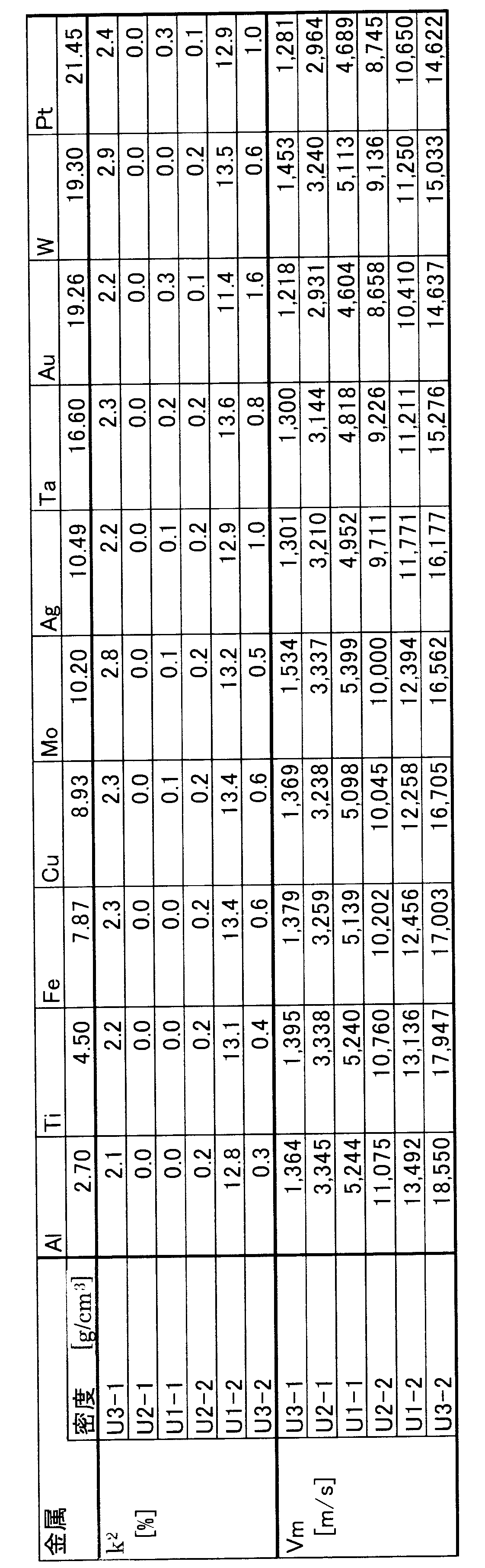
なお、パワーフロー角PFAは、表5に示したいずれの例においても0°であった。表5から明らかなように、Al、Ti、Fe、Cu、Mo、Ag、Ta、Au、W及びPtのいずれを用いた場合においても、U2-1、U1-2、U2-2、U3-1の各モードの電気機械結合係数k2は2%以下と低いことがわかる。従って、電極材料は特に限定されず、上記いずれの金属を用いても、スプリアスとなる他のモードの影響を効果的に抑制でき、かつPFAの絶対値を小さくし得ることがわかる。
〔第2の実施形態〕
図2は、本発明の第2の実施形態に係る弾性波装置の要部を示す模式的正面断面図である。図2は、第1の実施形態において示した図1(a)の模式的断面図に相当する図である。
図2は、本発明の第2の実施形態に係る弾性波装置の要部を示す模式的正面断面図である。図2は、第1の実施形態において示した図1(a)の模式的断面図に相当する図である。
弾性波装置21では、圧電薄膜4の上面に誘電体膜3が形成されている。すなわち、IDT電極5を覆うように、誘電体膜3が形成されている。このように、本発明においては、誘電体膜3が、圧電薄膜4の上面に形成されていてもよい。
図3(a)及び(b)は、本発明の第3の実施形態及びその変形例に係る弾性波装置の模式的正面断面図である。図3(a)及び(b)は、第1の実施形態について示した図1(a)に相当する図である。
第3の実施形態の弾性波装置31では、誘電体膜3が圧電薄膜4の下面側に形成されている。また、図3(b)の変形例の弾性波装置31Aのように、圧電薄膜4の下面にIDT電極5が形成されていてもよい。すなわち、IDT電極5は、凹部2aにより形成されている空間に臨むように形成されている。このように、IDT電極5は、圧電薄膜4の下面に形成されていてもよい。
また、図3(b)では、圧電薄膜4上に誘電体膜3が積層されている。
なお、第2~第3の実施形態では、誘電体膜3が圧電薄膜4の上面または下面に形成されているが、上面及び下面の双方に形成されていてもよい。さらに、本発明では、誘電体膜3は、必須ではなく、誘電体膜3を設けずともよい。誘電体膜3は、酸化ケイ素、窒化ケイ素、窒化アルミニウムなどの適宜の誘電体材料により形成することができる。
また、誘電体膜3を形成した構造では、誘電体膜3をイオンミリングなどにより削ることにより、周波数調整を行うことができる。この場合、周波数調整を容易に行い得るため、誘電体膜3が上面に露出している第2の実施形態及び第3の実施形態の変形例である図3(b)場合、周波数調整をより一層容易に行うことができる。
加えて、誘電体膜3を圧電薄膜4に積層することにより、周波数温度係数TCFの絶対値を小さくすることができる。これを、図69を参照して説明する。
図69は、本発明に従って構成された種々の弾性波装置における圧電薄膜4の規格化膜厚と、周波数温度係数TCFとの関係を示す図である。
圧電薄膜4としては、オイラー角(0°,33°,0°)のLiTaO3薄膜を用いた。また、IDT電極5については、20nmのTi膜及び200nmの厚みのAl膜を順に成膜することにより形成した。また、伝搬する弾性波の波長λは3.5μmである。誘電体膜3の膜厚は、175nmとした。なお、Ti膜はAl膜をLiTaO3に密着させる役割を担う。
LiTaO3からなる圧電薄膜4の規格化膜厚を種々異ならせ、弾性波装置を作製し、その周波数温度係数TCFを測定した。用意したサンプルは以下の通りである。
実施例1:第1の実施形態と同様とした弾性波装置。
実施例2:図3(a)に示した第3の実施形態に従って、但し、誘電体膜3として、厚み0.05λのSiO2膜を形成した。
実施例3:図3(a)に示した第3の実施形態と同様にして、但し、誘電体膜3として、厚み0.05λのSiN膜を形成した。
実施例4:図3(a)に示した第3の実施形態と同様にして、但し、誘電体膜3として、厚み0.05λのAlN膜を形成した。
図69から明らかなように、圧電薄膜4の規格化膜厚が、0.30を超えると、誘電体膜3を形成していない実施例1では、TCFの絶対値が60ppm/℃以上と大きくなる。これに対して、誘電体膜3を形成してなる実施例2~4では、圧電薄膜4の広い膜厚範囲において、TCFの絶対値自体を小さくすることができる。しかも、圧電薄膜4の膜厚が厚くなったとしても、TCFの絶対値を32ppm/℃以下と小さくし得ることがわかる。
また、図2に示した第2の実施形態に従って、弾性波装置を作製し、その周波数温度係数TCFを測定した。圧電薄膜4としては、オイラー角(0°,33°,0°)、厚み0.18λのLiTaO3薄膜を用いた。また、伝搬する弾性波の波長λは3.5μmで、IDT電極5については、20nmのTi膜及び35nmのPt、35nmの厚みのAl膜を順に成膜することにより形成した。さらに、IDT上部に誘電体膜3を形成しない構造と、形成した構造を作製した。誘電体膜3を形成した構造では誘電体膜3はSiO2とし、膜厚は105nmとした。誘電体膜3のない構造のTCFは-8.6[ppm/℃]であり、誘電体膜3を形成した構造のTCFは-1.4[ppm/℃]であった。IDT上に誘電体を形成した場合でもTCFの絶対値を小さくし得ることがわかる。
LiTaO3の弾性定数Cijの一次の温度係数(1/x)(δx/δT)はマイナスの値である。これに対して、SiO2の弾性定数の一次の温度係数はプラスの値である。従って、SiO2を積層することにより、弾性定数の温度係数のプラスとマイナスが打ち消しあい、結果としてTCFの絶対値を小さくすることができる。加えて、LiTaO3の線膨張係数に比べて、SiO2、SiN及びAlNなどの誘電体の線膨張係数は小さい。さらに、LiTaO3からなる圧電薄膜4の膜厚が非常に小さい。従って、誘電体膜3の線膨張係数の影響を大きく受けることになり、実質的な弾性波伝搬方向の線膨張係数が小さくなると考えられる。それによっても、誘電体膜3の形成により、TCFの絶対値が小さくなっていると考えられる。
なお、LiTaO3の線膨張係数は16ppm/℃である。SiO2の線膨張係数は0.6ppm/℃、SiNの線膨張係数は3ppm/℃、AlNの線膨張係数は4~5ppm/℃程度である。
なお、図3(a)の弾性波装置31では、圧電薄膜4の下面に誘電体膜3が形成されており、上面にIDT電極5が形成されている。この構造では、好ましくは、誘電体膜3が、LiTaO3からなる圧電薄膜4に引っ張り応力を与えるように形成されることが望ましい。それによって、IDT電極5が突出されている上面側が凸状となる。この場合には、凹部2a上に位置している板波が伝搬する部分が凹部2aの下方の支持層2に接触したり、接着剤層などの他の部分に接触するおそれを低減することができる。従って、板波が安定に伝搬する。上記誘電体膜3と圧電薄膜4とからなる積層膜がIDT電極5側において、凹状となった場合には、板波が伝搬する部分が凹部2aの下方の支持層2の一部に接触したり、図示しない接着剤層に接触したりするおそれがある。また、静電力により、宙に浮いている板波が伝搬する部分が支持層2に接触したりするおそれもある。
なお、引っ張り応力とは、誘電体膜3による応力が、LiTaO3からなる圧電薄膜4と誘電体膜3との界面において、LiTaO3からなる圧電薄膜4を圧縮するように働く方向の応力である。
特に、誘電体膜3がAlNからなる場合、成膜時の圧力を調整することにより、誘電体膜3のLiTaO3に対する応力を、圧縮応力から引っ張り応力までの広い範囲で容易に調整することができる。従って、AlN膜を誘電体膜3として用いることが好ましい。
LiTaO3は、強誘電体であるため、焦電性を有している。従って、温度変化や圧力変化が与えられると、圧電薄膜4の表面に焦電荷が発生するおそれがある。焦電荷により、IDT電極5が破壊されないように、圧電薄膜4にある程度の導電性を持たせることが望ましい。IDT電極の絶縁抵抗Rが1MΩ以下であると、圧電薄膜4上の焦電荷が効果的に中和され、IDT電極5の破壊を抑制することができる。
他方、IDT電極の絶縁抵抗が、弾性波装置1を接続する電気回路の終端インピーダンスの50倍よりも小さくなると、LiTaO3からなる圧電薄膜4を介して振動エネルギーの漏洩が生じやすくなる。従って、絶縁抵抗は、終端インピーダンスの50倍よりも大きいことが望ましい。
また、LiTaO3からなる圧電薄膜4の厚みは特に限定されない。もっとも、圧電薄膜4の厚みが50nm以下であると、中空構造としての強度が弱くなり、実用上信頼性に問題がある。従って、LiTaO3からなる圧電薄膜の厚みは50nm以上であることが望ましい。なお、圧電薄膜4の上限はU1成分を変位の主成分とする板波の二次モードの音速を十分高くするため、0.3λ以下であることが望ましい。
第1の本実施形態の弾性波装置1では、凹部2a上に圧電薄膜4及びIDT電極5が配置され、IDT電極5の左右に反射器を配置した1つの弾性波共振子が構成されている。もっとも、本発明においては、図71に示すように、複数の弾性波装置1,1Aが組み合わされていてもよい。特に、好ましくは、支持層2上において、複数の凹部2aを形成し、各凹部2aが設けられている位置において、本実施形態と同様に、弾性波共振子などの弾性波素子を形成することが望ましい。この場合、圧電薄膜4としては、同一のカット角の圧電薄膜4を用いることが望ましく、それによって製造工程の簡略化を図ることができる。
なお、複数の弾性波素子としては、本実施形態のように、弾性波共振子を複数用いてもよく、あるいは共振子型フィルタなどの複数の弾性波素子を組み合わせてフィルタを構成してもよい。さらに、これらの弾性波素子と他の素子を組み合わせてデュプレクサなどを構成してもよい。
上記のような複数の弾性波共振子を組み合わせて構成してなるフィルタとしては、ラダー型フィルタやラチス型フィルタなどを挙げることができる。
また、図71における弾性波装置1における伝搬方位ψを、弾性波装置1Aの伝搬方位ψと異ならせてもよい。板波は非漏洩タイプの伝搬モードであるため、伝搬方位ψを異ならせた場合でも、減衰しない。従って、弾性波共振子のQが劣化しない。
3以上の弾性波素子を組み合わせる場合には、少なくとも1つの弾性波素子の伝搬方位を、残りの内の少なくとも1つの弾性波素子の伝搬方位と異ならせてもよい。
また、同一カット角の圧電薄膜4を用い、該圧電薄膜4内において、伝搬方位ψを変更することにより、電気機械結合係数k2を異ならせることができる。
よって、複数の弾性波素子を構成した場合、それぞれにおいて、最適な電気機械結合係数k2を容易に設定することができる。従って、フィルタなどの設計の自由度を大幅に高めることができる。
〔製造方法〕
本発明に係る弾性波装置の製造方法は、特に限定されないが、図70を参照してその一例を説明する。
本発明に係る弾性波装置の製造方法は、特に限定されないが、図70を参照してその一例を説明する。
図70(a)~(i)は、本発明のさらに他の第1の実施形態の弾性波装置の製造方法の一例を示す各模式的正面断面図である。
また、図70(a)に示すように、LiTaO3ウエハ41を用意する。次に、LiTaO3ウエハ41の上面に、100keVで加速したH+イオンを8×10¹⁶at/cm2の濃度で注入する。上記水素イオンを注入すると、LiTaO3ウエハ41において水素イオン濃度が厚み方向において分布を有する。最も水素イオン濃度が高い部分を、水素イオン高濃度注入部分41aとして、破線で示す。水素イオン高濃度注入部分41aが形成される深さは、LiTaO3ウエハ41の上面から一定の深さとされている。この水素イオン高濃度注入部分41aの深さは、最終的に形成したい圧電薄膜4の厚みより少し深い位置とする。
後述するように、水素イオン高濃度注入部分41aにおいて、加熱により、圧電薄膜4Aと、残りのLiTaO3ウエハ部分41bとが分離する。そして、上記水素イオン高濃度注入部分41aから水素イオン注入側のウエハ表面までの少なくとも一部が圧電薄膜として用いられるものとなる。よって、このような分離実験を予め行うことにより、最終的に形成したい圧電薄膜4の厚みに応じて、水素イオン高濃度注入部分41aの深さを制御することができる。あるいは、水素イオン注入後にLiTaO3ウエハ41の内部の水素イオン濃度を測定することにより、水素イオン高濃度注入部分41aの位置を確かめてもよい。
なお、水素イオン高濃度注入部分41aの深さは、最終的に形成したい圧電薄膜4の厚みより少し深い位置とすることが好ましい。そのため、本実施形態では、上記のように、水素イオン高濃度注入部分41aの深さを、圧電薄膜4の厚みよりも少し深くしている。この場合、圧電性回復工程後に、上記水素イオン高濃度注入部分41a側から研磨等により厚みを減らす加工工程を実施する。それによって、圧電性が優れ、かつ圧電性が均一な圧電薄膜4を得ることができる。
次に、圧電薄膜4A側のLiTaO3ウエハ表面に、図70(c)に示すように、犠牲層42としてCuを蒸着法により2μmの厚さで形成する。犠牲層42は、例えばエッチングにより消失する適宜の材料により形成することができる。犠牲層42を形成した後に、支持層2としてSiO2をスパッタ法により5μmほど形成する。
次に、図70(d)に示すように、支持層2の下面に、支持ウエハ2Aとして、圧電層と同じオイラー角のLiTaO3ウエハを接合する。この支持ウエハ2Aは、LiTaO3ウエハだけでなく、例えば誘電体セラミックウエハや高抵抗Siウエハでもよいし、形成せずともよい。しかる後、500℃の加熱下で、図70(e)に示すように、水素イオン高濃度注入部分41aを境にして、圧電薄膜4AとLiTaO3ウエハ41の残りの部分41bとを分離する。上記水素イオン高濃度注入部分41aでは、加熱により分離を容易に行うことができる。このような技術は、例えば、特開2010-109949号公報に開示されている。それによって、図70(f)に示すように、支持層2上に、任意のオイラー角で厚みの薄い圧電薄膜4Aをウエハからスライシングでき、均一な厚みで形成することができる。
しかる後、分離した圧電薄膜4Aの表面を0.1μm研磨し、かつ加熱により圧電性を回復させる。それによって、最終的な圧電薄膜4を得る。そして、圧電薄膜4上に、図70(g)に示すように、IDT電極5を形成する。さらに、圧電薄膜4Aを図70(h)に示すように、パターニングし、犠牲層42の一部を露出させる開口部6,7を形成する。次に、図70(i)に示すように、開口部を通じてエッチングにより犠牲層42を消失させる。このようにして、第1の実施形態と同様の弾性波装置を得ることができる。また、前記製造方法において、イオン注入後の圧電薄膜4Aの表面に誘電体膜3を形成し、その後犠牲層を形成し、同様の加工を行えば、圧電膜の下面に誘電体膜のある図3(a)に示した第3の実施形態と同様の弾性波装置を得ることができる。
1,1A…弾性波装置
2…支持層
2A…支持ウエハ
2a…凹部
3…誘電体膜
4…圧電薄膜
4A…圧電薄膜
5…IDT電極
6,7…開口部
21…弾性波装置
31,31A…弾性波装置
41…LiTaO3ウエハ
41a…水素イオン高濃度注入部分
41b…部分
42…犠牲層
A1~A12…領域
B1~B12…領域
C1~C12…領域
D1~D12…領域
R1~R7…領域
2…支持層
2A…支持ウエハ
2a…凹部
3…誘電体膜
4…圧電薄膜
4A…圧電薄膜
5…IDT電極
6,7…開口部
21…弾性波装置
31,31A…弾性波装置
41…LiTaO3ウエハ
41a…水素イオン高濃度注入部分
41b…部分
42…犠牲層
A1~A12…領域
B1~B12…領域
C1~C12…領域
D1~D12…領域
R1~R7…領域
Claims (10)
- 上面に開いた凹部または貫通孔が形成されている支持層と、
前記支持層の前記凹部または貫通孔上に至るように前記支持層上に形成された圧電薄膜と、
該圧電薄膜の前記凹部または貫通孔上に至っている領域において、前記圧電薄膜の上面及び下面の内の少なくとも一方の面に形成されたIDT電極とを備え、
U1成分を変位の主成分とする板波の二次モードを用いており、前記圧電薄膜がLiTaO3からなり、該LiTaO3のオイラー角(φ,θ,ψ)が、図4~図10において実線で囲んである領域R1~R7のいずれかの範囲内にある、弾性波装置。 - 前記IDT電極がAlまたはAlを主成分とする合金からなり、IDT電極の膜厚をHとしたとき、H≦0.08λ(但し、λはU1成分を主成分とする板波の二次モードの波長)である、請求項1に記載の弾性波装置。
- 前記圧電薄膜の上面及び下面の内の少なくとも一方面に積層された誘電体膜をさらに備え、該誘電体膜の線膨張係数が、LiTaO3の線膨張係数よりも小さい、請求項1または2に記載の弾性波装置。
- 前記誘電体膜が酸化ケイ素からなる、請求項3に記載の弾性波装置。
- 前記圧電薄膜の上面に前記IDT電極が形成されており、前記圧電薄膜の下面に前記誘電体膜が形成されており、前記誘電体膜が前記圧電薄膜に対して引っ張り方向応力を与える誘電体材料からなる、請求項3または4に記載の弾性波装置。
- 前記IDT電極間の電気抵抗が、弾性波装置を接続する電気回路の終端インピーダンスの50倍以上であり、かつ1MΩ以下である、請求項1~5のいずれか1項に記載の弾性波装置。
- 前記圧電薄膜の厚みが50nm以上、0.3λ(但し、λはU1成分を主成分とする板波の二次モードの波長)以下の範囲にある、請求項1~6のいずれか1項に記載の弾性波装置。
- 請求項1~7のいずれか1項に記載の弾性波装置を複数備える、弾性波装置。
- 前記複数の弾性波装置の内の少なくとも1つの弾性波装置における伝搬方位ψが、残りの少なくとも1つの弾性波装置の伝搬方位ψと異なっている、請求項8に記載の弾性波装置。
- 請求項1~9のいずれか1項に記載の弾性波装置の製造方法であって、
LiTaO3基板の表面からイオンを注入し、イオン注入部分をLiTaO3基板の片面側に形成する工程と、
前記イオン注入した側の面の一部に犠牲層を形成する工程と、
前記イオン注入した側の面及び前記犠牲層を覆うように絶縁体を形成して支持層とする工程と、
加熱により、前記LiTaO3基板を前記イオン注入部分で分離し、LiTaO3基板から分離された圧電薄膜構造体を形成する工程と、
前記犠牲層を消失させて、前記圧電薄膜の下方に前記支持層の凹部を形成する工程と、
前記圧電薄膜の上面または下面の内少なくとも一方の面にIDT電極を形成する工程とを備える、弾性波装置の製造方法。
Priority Applications (2)
| Application Number | Priority Date | Filing Date | Title |
|---|---|---|---|
| JP2012546849A JP5601377B2 (ja) | 2010-11-30 | 2011-11-28 | 弾性波装置及びその製造方法 |
| US13/900,743 US9748923B2 (en) | 2010-11-30 | 2013-05-23 | Elastic wave device and manufacturing method for same |
Applications Claiming Priority (2)
| Application Number | Priority Date | Filing Date | Title |
|---|---|---|---|
| JP2010266538 | 2010-11-30 | ||
| JP2010-266538 | 2010-11-30 |
Related Child Applications (1)
| Application Number | Title | Priority Date | Filing Date |
|---|---|---|---|
| US13/900,743 Continuation US9748923B2 (en) | 2010-11-30 | 2013-05-23 | Elastic wave device and manufacturing method for same |
Publications (1)
| Publication Number | Publication Date |
|---|---|
| WO2012073871A1 true WO2012073871A1 (ja) | 2012-06-07 |
Family
ID=46171803
Family Applications (1)
| Application Number | Title | Priority Date | Filing Date |
|---|---|---|---|
| PCT/JP2011/077335 Ceased WO2012073871A1 (ja) | 2010-11-30 | 2011-11-28 | 弾性波装置及びその製造方法 |
Country Status (3)
| Country | Link |
|---|---|
| US (1) | US9748923B2 (ja) |
| JP (1) | JP5601377B2 (ja) |
| WO (1) | WO2012073871A1 (ja) |
Cited By (46)
| Publication number | Priority date | Publication date | Assignee | Title |
|---|---|---|---|---|
| CN103532513A (zh) * | 2012-07-04 | 2014-01-22 | 太阳诱电株式会社 | 兰姆波器件及其制造方法 |
| WO2015137089A1 (ja) * | 2014-03-14 | 2015-09-17 | 株式会社村田製作所 | 弾性波装置 |
| WO2016052129A1 (ja) * | 2014-09-30 | 2016-04-07 | 株式会社村田製作所 | 弾性波装置及びその製造方法 |
| WO2016093020A1 (ja) * | 2014-12-08 | 2016-06-16 | 株式会社村田製作所 | 圧電デバイス、及び圧電デバイスの製造方法 |
| WO2016103925A1 (ja) * | 2014-12-25 | 2016-06-30 | 株式会社村田製作所 | 弾性波装置及びその製造方法 |
| WO2016147687A1 (ja) * | 2015-03-13 | 2016-09-22 | 株式会社村田製作所 | 弾性波装置及びその製造方法 |
| WO2017212774A1 (ja) * | 2016-06-07 | 2017-12-14 | 株式会社村田製作所 | 弾性波装置及びその製造方法 |
| WO2018146883A1 (ja) * | 2017-02-10 | 2018-08-16 | 株式会社村田製作所 | 弾性波装置、高周波フロントエンド回路及び通信装置 |
| WO2018163805A1 (ja) * | 2017-03-09 | 2018-09-13 | 株式会社村田製作所 | 弾性波装置、高周波フロントエンド回路及び通信装置 |
| KR20190109522A (ko) * | 2017-03-09 | 2019-09-25 | 가부시키가이샤 무라타 세이사쿠쇼 | 탄성파 장치, 고주파 프론트 엔드 회로 및 통신 장치 |
| US10469053B2 (en) | 2014-12-18 | 2019-11-05 | Murata Manufacturing Co., Ltd. | Elastic wave device and manufacturing method for the same |
| JPWO2020130128A1 (ja) * | 2018-12-21 | 2021-02-15 | 京セラ株式会社 | 弾性波装置、分波器および通信装置 |
| WO2021060512A1 (ja) * | 2019-09-27 | 2021-04-01 | 株式会社村田製作所 | 弾性波装置 |
| JPWO2021002047A1 (ja) * | 2019-07-03 | 2021-09-13 | 日本碍子株式会社 | 接合体および弾性波素子 |
| WO2021187537A1 (ja) * | 2020-03-18 | 2021-09-23 | 株式会社村田製作所 | 弾性波装置 |
| WO2022014493A1 (ja) * | 2020-07-15 | 2022-01-20 | 株式会社村田製作所 | 弾性波装置 |
| WO2022019170A1 (ja) * | 2020-07-22 | 2022-01-27 | 株式会社村田製作所 | 弾性波装置 |
| WO2022071605A1 (ja) * | 2020-10-02 | 2022-04-07 | 株式会社村田製作所 | 弾性波装置及び弾性波装置の製造方法 |
| WO2022085581A1 (ja) * | 2020-10-23 | 2022-04-28 | 株式会社村田製作所 | 弾性波装置 |
| WO2022102719A1 (ja) * | 2020-11-13 | 2022-05-19 | 株式会社村田製作所 | 弾性波装置 |
| WO2022102619A1 (ja) * | 2020-11-11 | 2022-05-19 | 株式会社村田製作所 | 弾性波装置 |
| WO2022102417A1 (ja) * | 2020-11-11 | 2022-05-19 | 株式会社村田製作所 | 弾性波装置 |
| WO2022102720A1 (ja) * | 2020-11-13 | 2022-05-19 | 株式会社村田製作所 | 弾性波装置 |
| WO2022131216A1 (ja) * | 2020-12-14 | 2022-06-23 | 株式会社村田製作所 | 弾性波装置 |
| WO2022168937A1 (ja) * | 2021-02-05 | 2022-08-11 | 株式会社村田製作所 | 弾性波装置及び弾性波装置の製造方法 |
| WO2022186202A1 (ja) * | 2021-03-01 | 2022-09-09 | 株式会社村田製作所 | 弾性波装置 |
| WO2022190743A1 (ja) * | 2021-03-10 | 2022-09-15 | 株式会社村田製作所 | 弾性波装置 |
| WO2022211096A1 (ja) * | 2021-03-31 | 2022-10-06 | 株式会社村田製作所 | 弾性波装置及び弾性波装置の製造方法 |
| WO2022211103A1 (ja) * | 2021-03-31 | 2022-10-06 | 株式会社村田製作所 | 弾性波装置及び弾性波装置の製造方法 |
| WO2022211055A1 (ja) * | 2021-03-31 | 2022-10-06 | 株式会社村田製作所 | 弾性波装置 |
| WO2022211104A1 (ja) * | 2021-03-31 | 2022-10-06 | 株式会社村田製作所 | 弾性波装置 |
| WO2022210941A1 (ja) * | 2021-03-31 | 2022-10-06 | 株式会社村田製作所 | 弾性波装置 |
| WO2022209525A1 (ja) * | 2021-03-31 | 2022-10-06 | 株式会社村田製作所 | 弾性波装置 |
| WO2022210378A1 (ja) * | 2021-03-31 | 2022-10-06 | 株式会社村田製作所 | 弾性波装置 |
| WO2022209862A1 (ja) * | 2021-04-02 | 2022-10-06 | 株式会社村田製作所 | 弾性波装置 |
| WO2022210293A1 (ja) * | 2021-03-31 | 2022-10-06 | 株式会社村田製作所 | 弾性波装置 |
| WO2022210809A1 (ja) * | 2021-03-31 | 2022-10-06 | 株式会社村田製作所 | 弾性波装置 |
| WO2022210683A1 (ja) * | 2021-03-31 | 2022-10-06 | 株式会社村田製作所 | 弾性波装置及びその製造方法 |
| JP2022176790A (ja) * | 2021-05-17 | 2022-11-30 | 太陽誘電株式会社 | 弾性波デバイス、ウエハ、フィルタおよびマルチプレクサ |
| WO2023058767A1 (ja) * | 2021-10-08 | 2023-04-13 | 株式会社村田製作所 | 弾性波装置 |
| WO2023058755A1 (ja) * | 2021-10-08 | 2023-04-13 | 株式会社村田製作所 | 弾性波装置および弾性波装置の製造方法 |
| WO2023085362A1 (ja) * | 2021-11-11 | 2023-05-19 | 株式会社村田製作所 | 弾性波装置 |
| JP2023113959A (ja) * | 2019-09-27 | 2023-08-16 | 株式会社村田製作所 | 弾性波装置 |
| WO2023190610A1 (ja) * | 2022-03-28 | 2023-10-05 | 株式会社村田製作所 | 弾性波装置 |
| WO2025004233A1 (ja) * | 2023-06-28 | 2025-01-02 | 国立大学法人東北大学 | 弾性波素子 |
| KR102956715B1 (ko) | 2022-02-16 | 2026-04-24 | 가부시키가이샤 무라타 세이사쿠쇼 | 후면 코팅을 가진 음향 공진기 튜닝 |
Families Citing this family (170)
| Publication number | Priority date | Publication date | Assignee | Title |
|---|---|---|---|---|
| FR3037443B1 (fr) | 2015-06-12 | 2018-07-13 | Soitec | Heterostructure et methode de fabrication |
| JP6601503B2 (ja) * | 2015-10-23 | 2019-11-06 | 株式会社村田製作所 | 弾性波装置、高周波フロントエンド回路及び通信装置 |
| JP2017224890A (ja) * | 2016-06-13 | 2017-12-21 | 株式会社村田製作所 | 弾性波装置 |
| SG11201903365SA (en) | 2016-10-20 | 2019-05-30 | Skyworks Solutions Inc | Elastic wave device with sub-wavelength thick piezoelectric layer |
| WO2018193830A1 (ja) * | 2017-04-17 | 2018-10-25 | 株式会社村田製作所 | 弾性波装置、高周波フロントエンド回路及び通信装置 |
| US11929731B2 (en) | 2018-02-18 | 2024-03-12 | Murata Manufacturing Co., Ltd. | Transversely-excited film bulk acoustic resonator with optimized electrode mark, and pitch |
| US11206009B2 (en) | 2019-08-28 | 2021-12-21 | Resonant Inc. | Transversely-excited film bulk acoustic resonator with interdigital transducer with varied mark and pitch |
| US11323090B2 (en) | 2018-06-15 | 2022-05-03 | Resonant Inc. | Transversely-excited film bulk acoustic resonator using Y-X-cut lithium niobate for high power applications |
| US11936358B2 (en) | 2020-11-11 | 2024-03-19 | Murata Manufacturing Co., Ltd. | Transversely-excited film bulk acoustic resonator with low thermal impedance |
| US11996827B2 (en) | 2018-06-15 | 2024-05-28 | Murata Manufacturing Co., Ltd. | Transversely-excited film bulk acoustic resonator with periodic etched holes |
| US12237826B2 (en) | 2018-06-15 | 2025-02-25 | Murata Manufacturing Co., Ltd. | Transversely-excited film bulk acoustic resonator with optimized electrode thickness, mark, and pitch |
| US11509279B2 (en) | 2020-07-18 | 2022-11-22 | Resonant Inc. | Acoustic resonators and filters with reduced temperature coefficient of frequency |
| US12040779B2 (en) | 2020-04-20 | 2024-07-16 | Murata Manufacturing Co., Ltd. | Small transversely-excited film bulk acoustic resonators with enhanced Q-factor |
| US10637438B2 (en) | 2018-06-15 | 2020-04-28 | Resonant Inc. | Transversely-excited film bulk acoustic resonators for high power applications |
| US11323089B2 (en) | 2018-06-15 | 2022-05-03 | Resonant Inc. | Filter using piezoelectric film bonded to high resistivity silicon substrate with trap-rich layer |
| US12088281B2 (en) | 2021-02-03 | 2024-09-10 | Murata Manufacturing Co., Ltd. | Transversely-excited film bulk acoustic resonator with multi-mark interdigital transducer |
| US10911023B2 (en) * | 2018-06-15 | 2021-02-02 | Resonant Inc. | Transversely-excited film bulk acoustic resonator with etch-stop layer |
| US11323096B2 (en) | 2018-06-15 | 2022-05-03 | Resonant Inc. | Transversely-excited film bulk acoustic resonator with periodic etched holes |
| US11146232B2 (en) | 2018-06-15 | 2021-10-12 | Resonant Inc. | Transversely-excited film bulk acoustic resonator with reduced spurious modes |
| US10491192B1 (en) * | 2018-06-15 | 2019-11-26 | Resonant Inc. | Transversely-excited film bulk acoustic resonator |
| US10756697B2 (en) | 2018-06-15 | 2020-08-25 | Resonant Inc. | Transversely-excited film bulk acoustic resonator |
| US10601392B2 (en) | 2018-06-15 | 2020-03-24 | Resonant Inc. | Solidly-mounted transversely-excited film bulk acoustic resonator |
| US10790802B2 (en) | 2018-06-15 | 2020-09-29 | Resonant Inc. | Transversely excited film bulk acoustic resonator using rotated Y-X cut lithium niobate |
| US12119808B2 (en) | 2018-06-15 | 2024-10-15 | Murata Manufacturing Co., Ltd. | Transversely-excited film bulk acoustic resonator package |
| US11264966B2 (en) | 2018-06-15 | 2022-03-01 | Resonant Inc. | Solidly-mounted transversely-excited film bulk acoustic resonator with diamond layers in Bragg reflector stack |
| US11728785B2 (en) | 2018-06-15 | 2023-08-15 | Murata Manufacturing Co., Ltd. | Transversely-excited film bulk acoustic resonator using pre-formed cavities |
| US10985728B2 (en) * | 2018-06-15 | 2021-04-20 | Resonant Inc. | Transversely-excited film bulk acoustic resonator and filter with a uniform-thickness dielectric overlayer |
| US12081187B2 (en) | 2018-06-15 | 2024-09-03 | Murata Manufacturing Co., Ltd. | Transversely-excited film bulk acoustic resonator |
| US12463619B2 (en) | 2018-06-15 | 2025-11-04 | Murata Manufacturing Co., Ltd. | Filter device |
| US12149227B2 (en) | 2018-06-15 | 2024-11-19 | Murata Manufacturing Co., Ltd. | Transversely-excited film bulk acoustic resonator package |
| US11967945B2 (en) * | 2018-06-15 | 2024-04-23 | Murata Manufacturing Co., Ltd. | Transversly-excited film bulk acoustic resonators and filters |
| US12040781B2 (en) | 2018-06-15 | 2024-07-16 | Murata Manufacturing Co., Ltd. | Transversely-excited film bulk acoustic resonator package |
| US10917072B2 (en) | 2019-06-24 | 2021-02-09 | Resonant Inc. | Split ladder acoustic wave filters |
| US11171629B2 (en) * | 2018-06-15 | 2021-11-09 | Resonant Inc. | Transversely-excited film bulk acoustic resonator using pre-formed cavities |
| US10998877B2 (en) * | 2018-06-15 | 2021-05-04 | Resonant Inc. | Film bulk acoustic resonator fabrication method with frequency trimming based on electric measurements prior to cavity etch |
| US12301212B2 (en) | 2018-06-15 | 2025-05-13 | Murata Manufacturing Co., Ltd. | XBAR resonators with non-rectangular diaphragms |
| TWI863193B (zh) * | 2018-06-15 | 2024-11-21 | 日商村田製作所股份有限公司 | 橫向激發薄膜體聲波共振器 |
| US12244295B2 (en) | 2018-06-15 | 2025-03-04 | Murata Manufacturing Co., Ltd. | Transversely-excited film bulk acoustic resonators with two-layer electrodes having a narrower top layer |
| US11201601B2 (en) | 2018-06-15 | 2021-12-14 | Resonant Inc. | Transversely-excited film bulk acoustic resonator with multiple diaphragm thicknesses and fabrication method |
| US12155371B2 (en) | 2021-03-29 | 2024-11-26 | Murata Manufacturing Co., Ltd. | Layout of xbars with multiple sub-resonators in series |
| US12155374B2 (en) | 2021-04-02 | 2024-11-26 | Murata Manufacturing Co., Ltd. | Tiled transversely-excited film bulk acoustic resonator high power filters |
| US10797675B2 (en) | 2018-06-15 | 2020-10-06 | Resonant Inc. | Transversely excited film bulk acoustic resonator using rotated z-cut lithium niobate |
| US12095441B2 (en) | 2018-06-15 | 2024-09-17 | Murata Manufacturing Co., Ltd. | Transversely excited film bulk acoustic resonator with recessed interdigital transducer fingers |
| US11909381B2 (en) | 2018-06-15 | 2024-02-20 | Murata Manufacturing Co., Ltd. | Transversely-excited film bulk acoustic resonators with two-layer electrodes having a narrower top layer |
| US11323095B2 (en) | 2018-06-15 | 2022-05-03 | Resonant Inc. | Rotation in XY plane to suppress spurious modes in XBAR devices |
| US11146238B2 (en) | 2018-06-15 | 2021-10-12 | Resonant Inc. | Film bulk acoustic resonator fabrication method |
| US11996822B2 (en) | 2018-06-15 | 2024-05-28 | Murata Manufacturing Co., Ltd. | Wide bandwidth time division duplex transceiver |
| US11349452B2 (en) | 2018-06-15 | 2022-05-31 | Resonant Inc. | Transversely-excited film bulk acoustic filters with symmetric layout |
| US11374549B2 (en) | 2018-06-15 | 2022-06-28 | Resonant Inc. | Filter using transversely-excited film bulk acoustic resonators with divided frequency-setting dielectric layers |
| US12184261B2 (en) | 2018-06-15 | 2024-12-31 | Murata Manufacturing Co., Ltd. | Transversely-excited film bulk acoustic resonator with a cavity having round end zones |
| US12119805B2 (en) | 2018-06-15 | 2024-10-15 | Murata Manufacturing Co., Ltd. | Substrate processing and membrane release of transversely-excited film bulk acoustic resonator using a sacrificial tub |
| US12009798B2 (en) | 2018-06-15 | 2024-06-11 | Murata Manufacturing Co., Ltd. | Transversely-excited film bulk acoustic resonators with electrodes having irregular hexagon cross-sectional shapes |
| US12095446B2 (en) | 2018-06-15 | 2024-09-17 | Murata Manufacturing Co., Ltd. | Transversely-excited film bulk acoustic resonator with optimized electrode thickness, mark, and pitch |
| US12132464B2 (en) | 2018-06-15 | 2024-10-29 | Murata Manufacturing Co., Ltd. | Filter using transversely-excited film bulk acoustic resonators with divided frequency-setting dielectric layers |
| US12218650B2 (en) | 2018-06-15 | 2025-02-04 | Murata Manufacturing Co., Ltd. | Transversely-excited film bulk acoustic resonator |
| US12237827B2 (en) | 2018-06-15 | 2025-02-25 | Murata Manufacturing Co., Ltd. | Solidly-mounted transversely-excited film bulk acoustic filters with multiple piezoelectric plate thicknesses |
| US12224732B2 (en) | 2018-06-15 | 2025-02-11 | Murata Manufacturing Co., Ltd. | Solidly-mounted transversely-excited film bulk acoustic resonators and filters for 27 GHz communications bands |
| US12113512B2 (en) | 2021-03-29 | 2024-10-08 | Murata Manufacturing Co., Ltd. | Layout of XBARs with multiple sub-resonators in parallel |
| US11228296B2 (en) | 2018-06-15 | 2022-01-18 | Resonant Inc. | Transversely-excited film bulk acoustic resonator with a cavity having a curved perimeter |
| US11323091B2 (en) | 2018-06-15 | 2022-05-03 | Resonant Inc. | Transversely-excited film bulk acoustic resonator with diaphragm support pedestals |
| US11949402B2 (en) | 2020-08-31 | 2024-04-02 | Murata Manufacturing Co., Ltd. | Resonators with different membrane thicknesses on the same die |
| US11349450B2 (en) | 2018-06-15 | 2022-05-31 | Resonant Inc. | Symmetric transversely-excited film bulk acoustic resonators with reduced spurious modes |
| US12283944B2 (en) | 2018-06-15 | 2025-04-22 | Murata Manufacturing Co., Ltd. | Transversely-excited film bulk acoustic resonator with recessed rotated-Y-X cut lithium niobate |
| US10992284B2 (en) | 2018-06-15 | 2021-04-27 | Resonant Inc. | Filter using transversely-excited film bulk acoustic resonators with multiple frequency setting layers |
| US11329628B2 (en) | 2020-06-17 | 2022-05-10 | Resonant Inc. | Filter using lithium niobate and lithium tantalate transversely-excited film bulk acoustic resonators |
| US10826462B2 (en) | 2018-06-15 | 2020-11-03 | Resonant Inc. | Transversely-excited film bulk acoustic resonators with molybdenum conductors |
| US10998882B2 (en) | 2018-06-15 | 2021-05-04 | Resonant Inc. | XBAR resonators with non-rectangular diaphragms |
| US11876498B2 (en) | 2018-06-15 | 2024-01-16 | Murata Manufacturing Co., Ltd. | Transversely-excited film bulk acoustic resonator with multiple diaphragm thicknesses and fabrication method |
| US11996825B2 (en) | 2020-06-17 | 2024-05-28 | Murata Manufacturing Co., Ltd. | Filter using lithium niobate and rotated lithium tantalate transversely-excited film bulk acoustic resonators |
| US12212306B2 (en) | 2018-06-15 | 2025-01-28 | Murata Manufacturing Co., Ltd. | Transversely-excited film bulk acoustic resonator with multiple diaphragm thicknesses and fabrication method |
| US12021496B2 (en) | 2020-08-31 | 2024-06-25 | Murata Manufacturing Co., Ltd. | Resonators with different membrane thicknesses on the same die |
| US11888463B2 (en) | 2018-06-15 | 2024-01-30 | Murata Manufacturing Co., Ltd. | Multi-port filter using transversely-excited film bulk acoustic resonators |
| US10819309B1 (en) | 2019-04-05 | 2020-10-27 | Resonant Inc. | Transversely-excited film bulk acoustic resonator package and method |
| US11870423B2 (en) | 2018-06-15 | 2024-01-09 | Murata Manufacturing Co., Ltd. | Wide bandwidth temperature-compensated transversely-excited film bulk acoustic resonator |
| US12191838B2 (en) | 2018-06-15 | 2025-01-07 | Murata Manufacturing Co., Ltd. | Solidly-mounted transversely-excited film bulk acoustic device and method |
| US12170516B2 (en) * | 2018-06-15 | 2024-12-17 | Murata Manufacturing Co., Ltd. | Filters using transversly-excited film bulk acoustic resonators with frequency-setting dielectric layers |
| US11916539B2 (en) | 2020-02-28 | 2024-02-27 | Murata Manufacturing Co., Ltd. | Split-ladder band N77 filter using transversely-excited film bulk acoustic resonators |
| US12375056B2 (en) | 2018-06-15 | 2025-07-29 | Murata Manufacturing Co., Ltd. | Transversely-excited film bulk acoustic resonators |
| US12191837B2 (en) | 2018-06-15 | 2025-01-07 | Murata Manufacturing Co., Ltd. | Solidly-mounted transversely-excited film bulk acoustic device |
| US11901878B2 (en) | 2018-06-15 | 2024-02-13 | Murata Manufacturing Co., Ltd. | Transversely-excited film bulk acoustic resonators with two-layer electrodes with a wider top layer |
| DE112019005403T5 (de) | 2018-10-31 | 2021-07-15 | Resonant Inc. | Fest montierter transversal angeregter akustischer filmvolumenresonator |
| US11901873B2 (en) | 2019-03-14 | 2024-02-13 | Murata Manufacturing Co., Ltd. | Transversely-excited film bulk acoustic resonator with partial BRAGG reflectors |
| CN113615083B (zh) * | 2019-03-14 | 2024-10-15 | 株式会社村田制作所 | 带有半λ介电层的横向激励的薄膜体声学谐振器 |
| US10911021B2 (en) | 2019-06-27 | 2021-02-02 | Resonant Inc. | Transversely-excited film bulk acoustic resonator with lateral etch stop |
| US12034423B2 (en) * | 2019-06-27 | 2024-07-09 | Murata Manufacturing Co., Ltd | XBAR frontside etch process using polysilicon sacrificial layer |
| DE102019119097B4 (de) * | 2019-07-15 | 2025-10-16 | Rf360 Singapore Pte. Ltd. | SAW-Resonator mit reduzierten Störmoden, elektroakustisches Filter und Multiplexer |
| US11329625B2 (en) | 2019-07-18 | 2022-05-10 | Resonant Inc. | Film bulk acoustic sensors using thin LN-LT layer |
| US11606078B2 (en) | 2019-07-18 | 2023-03-14 | Skyworks Solutions, Inc. | Acoustic wave resonator with rotated and tilted interdigital transducer electrode |
| US10862454B1 (en) | 2019-07-18 | 2020-12-08 | Resonant Inc. | Film bulk acoustic resonators in thin LN-LT layers |
| CN116545405A (zh) * | 2019-09-23 | 2023-08-04 | 株式会社村田制作所 | 用于大功率应用的横向激励薄膜体声波谐振器 |
| US12506462B2 (en) | 2020-02-28 | 2025-12-23 | Murata Manufacturing Co., Ltd. | Transversely-excited film bulk acoustic resonator with multi-pitch interdigital transducer |
| US12255625B2 (en) | 2020-02-28 | 2025-03-18 | Murata Manufacturing Co., Ltd. | Filter using transversely-excited film bulk acoustic resonators with inductively coupled sub-resonators |
| KR102414496B1 (ko) * | 2020-03-16 | 2022-06-28 | 가부시키가이샤 무라타 세이사쿠쇼 | 탄성파 장치 |
| US12341493B2 (en) | 2020-04-20 | 2025-06-24 | Murata Manufacturing Co., Ltd. | Low loss transversely-excited film bulk acoustic resonators and filters |
| US12278617B2 (en) | 2020-04-20 | 2025-04-15 | Murata Manufacturing Co., Ltd. | High Q solidly-mounted transversely-excited film bulk acoustic resonators |
| US12341490B2 (en) | 2020-04-20 | 2025-06-24 | Murata Manufacturing Co., Ltd. | Low loss transversely-excited film bulk acoustic resonators and filters |
| US11811391B2 (en) | 2020-05-04 | 2023-11-07 | Murata Manufacturing Co., Ltd. | Transversely-excited film bulk acoustic resonator with etched conductor patterns |
| US11469733B2 (en) | 2020-05-06 | 2022-10-11 | Resonant Inc. | Transversely-excited film bulk acoustic resonators with interdigital transducer configured to reduce diaphragm stress |
| US12074584B2 (en) * | 2020-05-28 | 2024-08-27 | Murata Manufacturing Co., Ltd. | Transversely-excited film bulk acoustic resonators with two-layer electrodes |
| US12267062B2 (en) | 2020-06-17 | 2025-04-01 | Murata Manufacturing Co., Ltd. | Transversely-excited film bulk acoustic resonators with three-layer electrodes |
| US10992282B1 (en) | 2020-06-18 | 2021-04-27 | Resonant Inc. | Transversely-excited film bulk acoustic resonators with electrodes having a second layer of variable width |
| US11742828B2 (en) | 2020-06-30 | 2023-08-29 | Murata Manufacturing Co., Ltd. | Transversely-excited film bulk acoustic resonator with symmetric diaphragm |
| US11482981B2 (en) | 2020-07-09 | 2022-10-25 | Resonanat Inc. | Transversely-excited film bulk acoustic resonators with piezoelectric diaphragm supported by piezoelectric substrate |
| WO2022014495A1 (ja) * | 2020-07-15 | 2022-01-20 | 株式会社村田製作所 | 弾性波装置 |
| US11264969B1 (en) | 2020-08-06 | 2022-03-01 | Resonant Inc. | Transversely-excited film bulk acoustic resonator comprising small cells |
| US11671070B2 (en) | 2020-08-19 | 2023-06-06 | Murata Manufacturing Co., Ltd. | Transversely-excited film bulk acoustic resonators using multiple dielectric layer thicknesses to suppress spurious modes |
| US11271539B1 (en) | 2020-08-19 | 2022-03-08 | Resonant Inc. | Transversely-excited film bulk acoustic resonator with tether-supported diaphragm |
| US11894835B2 (en) | 2020-09-21 | 2024-02-06 | Murata Manufacturing Co., Ltd. | Sandwiched XBAR for third harmonic operation |
| US11658639B2 (en) | 2020-10-05 | 2023-05-23 | Murata Manufacturing Co., Ltd. | Transversely-excited film bulk acoustic resonator matrix filters with noncontiguous passband |
| US11405017B2 (en) | 2020-10-05 | 2022-08-02 | Resonant Inc. | Acoustic matrix filters and radios using acoustic matrix filters |
| US11929733B2 (en) | 2020-10-05 | 2024-03-12 | Murata Manufacturing Co., Ltd. | Transversely-excited film bulk acoustic resonator matrix filters with input and output impedances matched to radio frequency front end elements |
| US11728784B2 (en) | 2020-10-05 | 2023-08-15 | Murata Manufacturing Co., Ltd. | Transversely-excited film bulk acoustic resonator matrix filters with split die sub-filters |
| US11476834B2 (en) | 2020-10-05 | 2022-10-18 | Resonant Inc. | Transversely-excited film bulk acoustic resonator matrix filters with switches in parallel with sub-filter shunt capacitors |
| US11405019B2 (en) | 2020-10-05 | 2022-08-02 | Resonant Inc. | Transversely-excited film bulk acoustic resonator matrix filters |
| US11463066B2 (en) | 2020-10-14 | 2022-10-04 | Resonant Inc. | Transversely-excited film bulk acoustic resonators with piezoelectric diaphragm supported by piezoelectric substrate |
| US20220140814A1 (en) * | 2020-10-30 | 2022-05-05 | Resonant Inc. | Transversely-excited film bulk acoustic resonators with integrated passive device |
| US12119806B2 (en) | 2020-10-30 | 2024-10-15 | Murata Manufacturing Co., Ltd. | Transversely-excited film bulk acoustic resonator with spiral interdigitated transducer fingers |
| US12255617B2 (en) | 2020-11-11 | 2025-03-18 | Murata Manufacturing Co., Ltd. | Solidly-mounted transversely-excited film bulk acoustic resonators with low thermal impedance |
| US12003226B2 (en) | 2020-11-11 | 2024-06-04 | Murata Manufacturing Co., Ltd | Transversely-excited film bulk acoustic resonator with low thermal impedance |
| US12431856B2 (en) | 2020-11-12 | 2025-09-30 | Murata Manufacturing Co., Ltd. | Transversely-excited film bulk acoustic resonator with reduced loss in the aperture direction |
| US12028039B2 (en) | 2020-11-13 | 2024-07-02 | Murata Manufacturing Co., Ltd. | Forming XBAR devices with excess piezoelectric material removed |
| US11496113B2 (en) | 2020-11-13 | 2022-11-08 | Resonant Inc. | XBAR devices with excess piezoelectric material removed |
| US12362725B2 (en) | 2020-11-13 | 2025-07-15 | Murata Manufacturing Co., Ltd. | Transversely-excited film bulk acoustic filters with excess piezoelectric material removed |
| US12255626B2 (en) | 2020-11-13 | 2025-03-18 | Murata Manufacturing Co., Ltd. | Solidly-mounted transversely-excited film bulk acoustic filters with excess piezoelectric material removed |
| US11405020B2 (en) | 2020-11-26 | 2022-08-02 | Resonant Inc. | Transversely-excited film bulk acoustic resonators with structures to reduce acoustic energy leakage |
| CN116671009A (zh) * | 2020-12-23 | 2023-08-29 | 株式会社村田制作所 | 弹性波装置 |
| US12166468B2 (en) | 2021-01-15 | 2024-12-10 | Murata Manufacturing Co., Ltd. | Decoupled transversely-excited film bulk acoustic resonators for high power filters |
| US12126318B2 (en) | 2021-01-15 | 2024-10-22 | Murata Manufacturing Co., Ltd. | Filters using decoupled transversely-excited film bulk acoustic resonators |
| US11239816B1 (en) | 2021-01-15 | 2022-02-01 | Resonant Inc. | Decoupled transversely-excited film bulk acoustic resonators |
| US12463615B2 (en) | 2021-01-21 | 2025-11-04 | Murata Manufacturing Co., Ltd | Transversely-excited film bulk acoustic resonators with improved coupling and reduced energy leakage |
| US12113510B2 (en) | 2021-02-03 | 2024-10-08 | Murata Manufacturing Co., Ltd. | Transversely-excited film bulk acoustic resonators with multiple piezoelectric membrane thicknesses on the same chip |
| US12308826B2 (en) | 2021-02-03 | 2025-05-20 | Murata Manufacturing Co., Ltd. | Bandpass filters using transversely-excited film bulk acoustic resonators |
| US12308825B2 (en) | 2021-02-12 | 2025-05-20 | Murata Manufacturing Co., Ltd | Transversely-excited film bulk acoustic resonators with narrow gaps between busbars and ends of interdigital transducer fingers |
| US12126328B2 (en) | 2021-03-24 | 2024-10-22 | Murata Manufacturing Co., Ltd. | Acoustic filters with shared acoustic tracks |
| US12355426B2 (en) | 2021-03-24 | 2025-07-08 | Murata Manufacturing Co., Ltd. | Acoustic filters with shared acoustic tracks |
| US12348216B2 (en) | 2021-03-24 | 2025-07-01 | Murata Manufacturing Co., Ltd. | Acoustic filters with shared acoustic tracks and cascaded series resonators |
| US12289099B2 (en) | 2021-03-24 | 2025-04-29 | Murata Manufacturing Co., Ltd. | Acoustic filters with shared acoustic tracks for series and shunt resonators |
| US12341492B2 (en) | 2021-03-29 | 2025-06-24 | Murata Manufacturing Co., Ltd. | Transversely-excited film bulk acoustic resonators with busbar side edges that form angles with a perimeter of the cavity |
| CN120454674A (zh) | 2021-03-30 | 2025-08-08 | 株式会社村田制作所 | 使用横向激发薄膜体声谐振器的用于6 GHz WI-FI的滤波器 |
| US12224735B2 (en) | 2021-03-30 | 2025-02-11 | Murata Manufacturing Co., Ltd. | Diplexer using decoupled transversely-excited film bulk acoustic resonators |
| WO2022210953A1 (ja) * | 2021-03-31 | 2022-10-06 | 株式会社村田製作所 | 弾性波装置 |
| US12249971B2 (en) | 2021-04-02 | 2025-03-11 | Murata Manufacturing Co., Ltd. | Transversely-excited film bulk acoustic resonators with solidly mounted resonator (SMR) pedestals |
| US12237823B2 (en) | 2021-04-02 | 2025-02-25 | Murata Manufacturing Co., Ltd. | Transversely-excited film bulk acoustic resonators with solidly mounted resonator (SMR) pedestals |
| US12255633B2 (en) | 2021-04-16 | 2025-03-18 | Murata Manufacturing Co., Ltd. | Filter using transversely-excited film bulk acoustic resonators |
| US12126316B2 (en) | 2021-04-16 | 2024-10-22 | Murata Manufacturing Co., Ltd | Transversely-excited film bulk acoustic resonator |
| WO2022224972A1 (ja) * | 2021-04-19 | 2022-10-27 | 株式会社村田製作所 | 弾性波装置及び弾性波装置の製造方法 |
| US12255607B2 (en) | 2021-04-30 | 2025-03-18 | Murata Manufacturing Co., Ltd. | Transversely-excited film bulk acoustic resonator with buried oxide strip acoustic confinement structures |
| US12160220B2 (en) | 2021-04-30 | 2024-12-03 | Murata Manufacturing Co., Ltd. | Transversely-excited film bulk acoustic resonator with oxide strip acoustic confinement structures |
| US12075700B2 (en) | 2021-05-07 | 2024-08-27 | Murata Manufacturing Co., Ltd. | Transversely-excited film bulk acoustic resonator fabrication using polysilicon pillars |
| US12057823B2 (en) | 2021-05-07 | 2024-08-06 | Murata Manufacturing Co., Ltd. | Transversely-excited film bulk acoustic resonator with concentric interdigitated transducer fingers |
| US12170513B2 (en) | 2021-06-30 | 2024-12-17 | Murata Manufacturing Co., Ltd. | Transversely-excited film bulk acoustic resonator with reduced substrate to contact bump thermal resistance |
| US12603639B2 (en) | 2021-08-02 | 2026-04-14 | Murata Manufacturing Co., Ltd. | Metal cavity for transversely-excited film bulk acoustic resonator (XBAR) |
| US12456962B2 (en) | 2021-09-24 | 2025-10-28 | Murata Manufacturing Co., Ltd. | Transversely-excited film bulk acoustic resonators wafer-level packaging using a dielectric cover |
| US12225387B2 (en) | 2021-09-29 | 2025-02-11 | Murata Manufacturing Co., Ltd. | Communications device with concurrent operation in 5GHZ and 6GHZ U-NII frequency ranges |
| US12451864B2 (en) | 2021-09-29 | 2025-10-21 | Murata Manufacturing Co., Ltd. | Transversely-excited film bulk acoustic resonators with curved shaped ends of fingers or opposing busbars |
| US12525951B2 (en) | 2021-10-01 | 2026-01-13 | Skyworks Solutions, Inc. | Surface acoustic wave device having a trapezoidal electrode |
| US12407326B2 (en) | 2021-11-04 | 2025-09-02 | Murata Manufacturing Co., Ltd. | Stacked die transversely-excited film bulk acoustic resonator (XBAR) filters |
| US12494768B2 (en) | 2021-12-28 | 2025-12-09 | Murata Manufacturing Co., Ltd. | Transversely-excited film bulk acoustic resonators with gap dielectric stripes in busbar-electrode gaps |
| US12424999B2 (en) | 2021-12-28 | 2025-09-23 | Murata Manufacturing Co., Ltd. | Transversely-excited film bulk acoustic resonators with gap dielectric stripes in busbar-electrode gaps |
| US20230208385A1 (en) | 2021-12-28 | 2023-06-29 | Skyworks Solutions, Inc. | Acoustic wave device with tilted interdigital transducer electrode |
| US12483226B2 (en) | 2021-12-29 | 2025-11-25 | Skyworks Solutions, Inc. | Acoustic wave device with tilted multilayer interdigital transducer electrode |
| CN114301422B (zh) * | 2021-12-31 | 2023-06-09 | 锐石创芯(重庆)科技有限公司 | 滤波器、多工器、射频前端及制造滤波器的方法 |
| US20230223910A1 (en) | 2022-01-13 | 2023-07-13 | Skyworks Solutions, Inc. | Method of making acoustic wave device with vertically mass loaded multi-layer interdigital transducer electrode for transverse mode suppression |
| US12413196B2 (en) | 2022-02-16 | 2025-09-09 | Murata Manufacturing Co., Ltd. | Tuning acoustic resonators with back-side coating |
| US12489417B2 (en) | 2022-04-12 | 2025-12-02 | Murata Manufacturing Co., Ltd. | Ladder filter with transversely-excited film bulk acoustic resonators having different pitches |
| WO2023200670A1 (en) * | 2022-04-12 | 2023-10-19 | Murata Manufacturing Co., Ltd. | Ladder filter with transversely-excited film bulk acoustic resonators having different pitches |
| US12549151B2 (en) | 2022-04-12 | 2026-02-10 | Murata Manufacturing Co., Ltd. | Transversely-excited film bulk acoustic resonator with thick dielectric layer for improved coupling |
| US12500572B2 (en) | 2022-04-15 | 2025-12-16 | Skyworks Solutions, Inc. | Multiplexer formed on multi-layer piezoelectric substrate and temperature compensated surface acoustic wave device dies |
| US12489415B2 (en) | 2022-10-19 | 2025-12-02 | Murata Manufacturing Co., Ltd. | Acoustic resonator lid for thermal transport |
| JP2025078470A (ja) * | 2023-11-08 | 2025-05-20 | 株式会社村田製作所 | 弾性波素子、弾性波フィルタ装置およびマルチプレクサ |
Citations (3)
| Publication number | Priority date | Publication date | Assignee | Title |
|---|---|---|---|---|
| JP2010056736A (ja) * | 2008-08-27 | 2010-03-11 | Murata Mfg Co Ltd | 電子部品及び電子部品の製造方法 |
| WO2010082571A1 (ja) * | 2009-01-15 | 2010-07-22 | 株式会社村田製作所 | 圧電デバイスおよび圧電デバイスの製造方法 |
| JP2010220204A (ja) * | 2009-02-17 | 2010-09-30 | Ngk Insulators Ltd | ラム波装置 |
Family Cites Families (7)
| Publication number | Priority date | Publication date | Assignee | Title |
|---|---|---|---|---|
| JP2002368576A (ja) | 2001-06-05 | 2002-12-20 | Fujitsu Media Device Kk | 弾性波素子 |
| WO2005060094A1 (ja) * | 2003-12-16 | 2005-06-30 | Murata Manufacturing Co., Ltd. | 弾性境界波装置 |
| US7319284B2 (en) * | 2005-09-02 | 2008-01-15 | Precision Instrument Development Center National Applied Research Laboratories | Surface acoustic wave device and method for fabricating the same |
| JP4793448B2 (ja) * | 2006-10-12 | 2011-10-12 | 株式会社村田製作所 | 弾性境界波装置 |
| CN102017407B (zh) * | 2008-04-30 | 2014-03-19 | 株式会社村田制作所 | 弹性边界波装置 |
| TWI381060B (zh) * | 2008-08-12 | 2013-01-01 | Univ Tatung | High frequency surface acoustic wave elements and their substrates |
| JP2010220164A (ja) * | 2009-03-19 | 2010-09-30 | Seiko Epson Corp | ラム波型共振子及び発振器 |
-
2011
- 2011-11-28 WO PCT/JP2011/077335 patent/WO2012073871A1/ja not_active Ceased
- 2011-11-28 JP JP2012546849A patent/JP5601377B2/ja active Active
-
2013
- 2013-05-23 US US13/900,743 patent/US9748923B2/en active Active
Patent Citations (3)
| Publication number | Priority date | Publication date | Assignee | Title |
|---|---|---|---|---|
| JP2010056736A (ja) * | 2008-08-27 | 2010-03-11 | Murata Mfg Co Ltd | 電子部品及び電子部品の製造方法 |
| WO2010082571A1 (ja) * | 2009-01-15 | 2010-07-22 | 株式会社村田製作所 | 圧電デバイスおよび圧電デバイスの製造方法 |
| JP2010220204A (ja) * | 2009-02-17 | 2010-09-30 | Ngk Insulators Ltd | ラム波装置 |
Cited By (75)
| Publication number | Priority date | Publication date | Assignee | Title |
|---|---|---|---|---|
| CN103532513A (zh) * | 2012-07-04 | 2014-01-22 | 太阳诱电株式会社 | 兰姆波器件及其制造方法 |
| JP2014013991A (ja) * | 2012-07-04 | 2014-01-23 | Taiyo Yuden Co Ltd | ラム波デバイスおよびその製造方法 |
| WO2015137089A1 (ja) * | 2014-03-14 | 2015-09-17 | 株式会社村田製作所 | 弾性波装置 |
| US10454448B2 (en) | 2014-03-14 | 2019-10-22 | Murata Manufacturing Co., Ltd. | Elastic wave device |
| WO2016052129A1 (ja) * | 2014-09-30 | 2016-04-07 | 株式会社村田製作所 | 弾性波装置及びその製造方法 |
| US10615774B2 (en) | 2014-09-30 | 2020-04-07 | Murata Manufacturing Co., Ltd. | Elastic wave device and manufacturing method therefor |
| JPWO2016052129A1 (ja) * | 2014-09-30 | 2017-05-18 | 株式会社村田製作所 | 弾性波装置及びその製造方法 |
| KR102058029B1 (ko) * | 2014-09-30 | 2019-12-20 | 가부시키가이샤 무라타 세이사쿠쇼 | 래더형 필터 및 그 제조 방법 |
| WO2016093020A1 (ja) * | 2014-12-08 | 2016-06-16 | 株式会社村田製作所 | 圧電デバイス、及び圧電デバイスの製造方法 |
| US10700262B2 (en) | 2014-12-08 | 2020-06-30 | Murata Manufacturing Co., Ltd. | Piezoelectric device and production method for piezoelectric device |
| US10469053B2 (en) | 2014-12-18 | 2019-11-05 | Murata Manufacturing Co., Ltd. | Elastic wave device and manufacturing method for the same |
| WO2016103925A1 (ja) * | 2014-12-25 | 2016-06-30 | 株式会社村田製作所 | 弾性波装置及びその製造方法 |
| US10530333B2 (en) | 2014-12-25 | 2020-01-07 | Murata Manufacturing Co., Ltd. | Acoustic wave device and manufacturing method for same |
| JPWO2016147687A1 (ja) * | 2015-03-13 | 2017-08-31 | 株式会社村田製作所 | 弾性波装置及びその製造方法 |
| WO2016147687A1 (ja) * | 2015-03-13 | 2016-09-22 | 株式会社村田製作所 | 弾性波装置及びその製造方法 |
| US11539344B2 (en) | 2016-06-07 | 2022-12-27 | Murata Manufacturing Co., Ltd. | Elastic wave device and method for producing the same |
| WO2017212774A1 (ja) * | 2016-06-07 | 2017-12-14 | 株式会社村田製作所 | 弾性波装置及びその製造方法 |
| KR20190099065A (ko) * | 2017-02-10 | 2019-08-23 | 가부시키가이샤 무라타 세이사쿠쇼 | 탄성파 장치, 고주파 프론트 엔드 회로 및 통신 장치 |
| KR102272692B1 (ko) * | 2017-02-10 | 2021-07-05 | 가부시키가이샤 무라타 세이사쿠쇼 | 탄성파 장치, 고주파 프론트 엔드 회로 및 통신 장치 |
| WO2018146883A1 (ja) * | 2017-02-10 | 2018-08-16 | 株式会社村田製作所 | 弾性波装置、高周波フロントエンド回路及び通信装置 |
| JPWO2018146883A1 (ja) * | 2017-02-10 | 2019-12-12 | 株式会社村田製作所 | 弾性波装置、高周波フロントエンド回路及び通信装置 |
| US10886896B2 (en) | 2017-02-10 | 2021-01-05 | Murata Manufacturing Co., Ltd. | Acoustic wave device, high-frequency front-end circuit, and communication device |
| WO2018163805A1 (ja) * | 2017-03-09 | 2018-09-13 | 株式会社村田製作所 | 弾性波装置、高周波フロントエンド回路及び通信装置 |
| KR20190109522A (ko) * | 2017-03-09 | 2019-09-25 | 가부시키가이샤 무라타 세이사쿠쇼 | 탄성파 장치, 고주파 프론트 엔드 회로 및 통신 장치 |
| JPWO2018163805A1 (ja) * | 2017-03-09 | 2019-12-26 | 株式会社村田製作所 | 弾性波装置、高周波フロントエンド回路及び通信装置 |
| US11611324B2 (en) | 2017-03-09 | 2023-03-21 | Murata Manufacturing Co., Ltd. | Acoustic wave device, high frequency front end circuit, and communication apparatus |
| KR20190109502A (ko) * | 2017-03-09 | 2019-09-25 | 가부시키가이샤 무라타 세이사쿠쇼 | 탄성파 장치, 고주파 프론트 엔드 회로 및 통신 장치 |
| KR102294196B1 (ko) | 2017-03-09 | 2021-08-27 | 가부시키가이샤 무라타 세이사쿠쇼 | 탄성파 장치, 고주파 프론트 엔드 회로 및 통신 장치 |
| JP2020162159A (ja) * | 2017-03-09 | 2020-10-01 | 株式会社村田製作所 | 弾性波装置、高周波フロントエンド回路及び通信装置 |
| KR102311140B1 (ko) | 2017-03-09 | 2021-10-12 | 가부시키가이샤 무라타 세이사쿠쇼 | 탄성파 장치, 고주파 프론트 엔드 회로 및 통신 장치 |
| JPWO2020130128A1 (ja) * | 2018-12-21 | 2021-02-15 | 京セラ株式会社 | 弾性波装置、分波器および通信装置 |
| JPWO2021002047A1 (ja) * | 2019-07-03 | 2021-09-13 | 日本碍子株式会社 | 接合体および弾性波素子 |
| JP7722414B2 (ja) | 2019-09-27 | 2025-08-13 | 株式会社村田製作所 | 弾性波装置 |
| US12603638B2 (en) | 2019-09-27 | 2026-04-14 | Murata Manufacturing Co., Ltd. | Acoustic wave device |
| US12389801B2 (en) | 2019-09-27 | 2025-08-12 | Murata Manufacturing Co., Ltd. | Acoustic wave device |
| US12324355B2 (en) | 2019-09-27 | 2025-06-03 | Murata Manufacturing Co., Ltd. | Acoustic wave device |
| JP2023113959A (ja) * | 2019-09-27 | 2023-08-16 | 株式会社村田製作所 | 弾性波装置 |
| WO2021060512A1 (ja) * | 2019-09-27 | 2021-04-01 | 株式会社村田製作所 | 弾性波装置 |
| WO2021187537A1 (ja) * | 2020-03-18 | 2021-09-23 | 株式会社村田製作所 | 弾性波装置 |
| US12267059B2 (en) | 2020-03-18 | 2025-04-01 | Murata Manufacturing Co., Ltd. | Acoustic wave device |
| WO2022014493A1 (ja) * | 2020-07-15 | 2022-01-20 | 株式会社村田製作所 | 弾性波装置 |
| US12301209B2 (en) | 2020-07-15 | 2025-05-13 | Murata Manufacturing Co., Ltd. | Acoustic wave device |
| WO2022019170A1 (ja) * | 2020-07-22 | 2022-01-27 | 株式会社村田製作所 | 弾性波装置 |
| WO2022071605A1 (ja) * | 2020-10-02 | 2022-04-07 | 株式会社村田製作所 | 弾性波装置及び弾性波装置の製造方法 |
| WO2022085581A1 (ja) * | 2020-10-23 | 2022-04-28 | 株式会社村田製作所 | 弾性波装置 |
| WO2022102619A1 (ja) * | 2020-11-11 | 2022-05-19 | 株式会社村田製作所 | 弾性波装置 |
| WO2022102417A1 (ja) * | 2020-11-11 | 2022-05-19 | 株式会社村田製作所 | 弾性波装置 |
| US12592677B2 (en) | 2020-11-11 | 2026-03-31 | Murata Manufacturing Co., Ltd. | Acoustic wave device |
| WO2022102719A1 (ja) * | 2020-11-13 | 2022-05-19 | 株式会社村田製作所 | 弾性波装置 |
| WO2022102720A1 (ja) * | 2020-11-13 | 2022-05-19 | 株式会社村田製作所 | 弾性波装置 |
| WO2022131216A1 (ja) * | 2020-12-14 | 2022-06-23 | 株式会社村田製作所 | 弾性波装置 |
| WO2022168937A1 (ja) * | 2021-02-05 | 2022-08-11 | 株式会社村田製作所 | 弾性波装置及び弾性波装置の製造方法 |
| WO2022186202A1 (ja) * | 2021-03-01 | 2022-09-09 | 株式会社村田製作所 | 弾性波装置 |
| WO2022190743A1 (ja) * | 2021-03-10 | 2022-09-15 | 株式会社村田製作所 | 弾性波装置 |
| US12537501B2 (en) | 2021-03-10 | 2026-01-27 | Murata Manufacturing Co., Ltd. | Acoustic wave device |
| WO2022211103A1 (ja) * | 2021-03-31 | 2022-10-06 | 株式会社村田製作所 | 弾性波装置及び弾性波装置の製造方法 |
| WO2022211055A1 (ja) * | 2021-03-31 | 2022-10-06 | 株式会社村田製作所 | 弾性波装置 |
| WO2022211096A1 (ja) * | 2021-03-31 | 2022-10-06 | 株式会社村田製作所 | 弾性波装置及び弾性波装置の製造方法 |
| WO2022210683A1 (ja) * | 2021-03-31 | 2022-10-06 | 株式会社村田製作所 | 弾性波装置及びその製造方法 |
| WO2022210809A1 (ja) * | 2021-03-31 | 2022-10-06 | 株式会社村田製作所 | 弾性波装置 |
| US12531542B2 (en) | 2021-03-31 | 2026-01-20 | Murata Manufacturing Co., Ltd. | Acoustic wave device |
| WO2022210293A1 (ja) * | 2021-03-31 | 2022-10-06 | 株式会社村田製作所 | 弾性波装置 |
| WO2022210378A1 (ja) * | 2021-03-31 | 2022-10-06 | 株式会社村田製作所 | 弾性波装置 |
| WO2022209525A1 (ja) * | 2021-03-31 | 2022-10-06 | 株式会社村田製作所 | 弾性波装置 |
| WO2022210941A1 (ja) * | 2021-03-31 | 2022-10-06 | 株式会社村田製作所 | 弾性波装置 |
| WO2022211104A1 (ja) * | 2021-03-31 | 2022-10-06 | 株式会社村田製作所 | 弾性波装置 |
| WO2022209862A1 (ja) * | 2021-04-02 | 2022-10-06 | 株式会社村田製作所 | 弾性波装置 |
| JP7710890B2 (ja) | 2021-05-17 | 2025-07-22 | 太陽誘電株式会社 | 弾性波デバイス、ウエハ、フィルタおよびマルチプレクサ |
| JP2022176790A (ja) * | 2021-05-17 | 2022-11-30 | 太陽誘電株式会社 | 弾性波デバイス、ウエハ、フィルタおよびマルチプレクサ |
| WO2023058755A1 (ja) * | 2021-10-08 | 2023-04-13 | 株式会社村田製作所 | 弾性波装置および弾性波装置の製造方法 |
| WO2023058767A1 (ja) * | 2021-10-08 | 2023-04-13 | 株式会社村田製作所 | 弾性波装置 |
| WO2023085362A1 (ja) * | 2021-11-11 | 2023-05-19 | 株式会社村田製作所 | 弾性波装置 |
| KR102956715B1 (ko) | 2022-02-16 | 2026-04-24 | 가부시키가이샤 무라타 세이사쿠쇼 | 후면 코팅을 가진 음향 공진기 튜닝 |
| WO2023190610A1 (ja) * | 2022-03-28 | 2023-10-05 | 株式会社村田製作所 | 弾性波装置 |
| WO2025004233A1 (ja) * | 2023-06-28 | 2025-01-02 | 国立大学法人東北大学 | 弾性波素子 |
Also Published As
| Publication number | Publication date |
|---|---|
| US20140152145A1 (en) | 2014-06-05 |
| US9748923B2 (en) | 2017-08-29 |
| JPWO2012073871A1 (ja) | 2014-05-19 |
| JP5601377B2 (ja) | 2014-10-08 |
Similar Documents
| Publication | Publication Date | Title |
|---|---|---|
| JP5601377B2 (ja) | 弾性波装置及びその製造方法 | |
| JP4178328B2 (ja) | 弾性境界波装置 | |
| CN103262410B (zh) | 弹性波装置及其制造方法 | |
| JP4356613B2 (ja) | 弾性境界波装置 | |
| JP4483785B2 (ja) | 弾性境界波装置 | |
| WO2008044411A1 (fr) | Dispositif à ondes limites élastiques | |
| JP5716831B2 (ja) | 圧電バルク波装置及びその製造方法 | |
| JPWO2005086345A1 (ja) | 弾性境界波装置 | |
| WO2007138840A1 (ja) | 弾性境界波装置 | |
| JPWO2011007690A1 (ja) | 弾性表面波装置 | |
| JPWO2013031748A1 (ja) | 圧電バルク波装置及びその製造方法 | |
| WO2006126327A1 (ja) | 弾性境界波装置 | |
| WO2013172287A1 (ja) | 弾性波装置 | |
| JP5716832B2 (ja) | 圧電バルク波装置及びその製造方法 | |
| KR100839788B1 (ko) | 탄성 경계파 장치 | |
| JP2012169760A (ja) | 弾性表面波装置 | |
| WO2008038506A1 (fr) | Dispositif d'onde acoustique limite | |
| KR20090130873A (ko) | 탄성경계파 장치 | |
| WO2009125536A1 (ja) | 弾性境界波装置及びその製造方法 | |
| US20240113682A1 (en) | Acoustic wave device | |
| JPWO2008093532A1 (ja) | 弾性境界波装置 | |
| JP2008187512A (ja) | 弾性境界波装置 | |
| JP2008187513A (ja) | 弾性境界波装置 | |
| JPWO2008093484A1 (ja) | 弾性境界波装置 | |
| JPWO2008093509A1 (ja) | 弾性境界波装置 |
Legal Events
| Date | Code | Title | Description |
|---|---|---|---|
| 121 | Ep: the epo has been informed by wipo that ep was designated in this application |
Ref document number: 11845380 Country of ref document: EP Kind code of ref document: A1 |
|
| ENP | Entry into the national phase |
Ref document number: 2012546849 Country of ref document: JP Kind code of ref document: A |
|
| NENP | Non-entry into the national phase |
Ref country code: DE |
|
| 122 | Ep: pct application non-entry in european phase |
Ref document number: 11845380 Country of ref document: EP Kind code of ref document: A1 |