JP2010056736A - 電子部品及び電子部品の製造方法 - Google Patents
電子部品及び電子部品の製造方法 Download PDFInfo
- Publication number
- JP2010056736A JP2010056736A JP2008218053A JP2008218053A JP2010056736A JP 2010056736 A JP2010056736 A JP 2010056736A JP 2008218053 A JP2008218053 A JP 2008218053A JP 2008218053 A JP2008218053 A JP 2008218053A JP 2010056736 A JP2010056736 A JP 2010056736A
- Authority
- JP
- Japan
- Prior art keywords
- piezoelectric
- piezoelectric body
- electronic component
- film
- insulator
- Prior art date
- Legal status (The legal status is an assumption and is not a legal conclusion. Google has not performed a legal analysis and makes no representation as to the accuracy of the status listed.)
- Granted
Links
- 238000004519 manufacturing process Methods 0.000 title claims abstract description 34
- 239000012212 insulator Substances 0.000 claims abstract description 38
- 238000005468 ion implantation Methods 0.000 claims abstract description 22
- 150000002500 ions Chemical class 0.000 claims abstract description 8
- 239000010410 layer Substances 0.000 claims description 57
- 239000012790 adhesive layer Substances 0.000 claims description 40
- 238000000034 method Methods 0.000 claims description 25
- 238000007751 thermal spraying Methods 0.000 claims description 8
- 230000003746 surface roughness Effects 0.000 claims description 7
- 238000004528 spin coating Methods 0.000 claims description 6
- 238000004544 sputter deposition Methods 0.000 claims description 5
- VYPSYNLAJGMNEJ-UHFFFAOYSA-N Silicium dioxide Chemical compound O=[Si]=O VYPSYNLAJGMNEJ-UHFFFAOYSA-N 0.000 claims description 3
- 229910052581 Si3N4 Inorganic materials 0.000 claims description 2
- 239000002184 metal Substances 0.000 claims description 2
- 229910044991 metal oxide Inorganic materials 0.000 claims description 2
- 150000004706 metal oxides Chemical class 0.000 claims description 2
- 150000004767 nitrides Chemical class 0.000 claims description 2
- 230000001902 propagating effect Effects 0.000 claims description 2
- HQVNEWCFYHHQES-UHFFFAOYSA-N silicon nitride Chemical compound N12[Si]34N5[Si]62N3[Si]51N64 HQVNEWCFYHHQES-UHFFFAOYSA-N 0.000 claims description 2
- 229910052814 silicon oxide Inorganic materials 0.000 claims description 2
- 239000010408 film Substances 0.000 description 91
- 239000000758 substrate Substances 0.000 description 22
- 239000013078 crystal Substances 0.000 description 15
- 238000005304 joining Methods 0.000 description 10
- 239000000463 material Substances 0.000 description 10
- 235000019687 Lamb Nutrition 0.000 description 8
- 230000003014 reinforcing effect Effects 0.000 description 7
- 238000005229 chemical vapour deposition Methods 0.000 description 6
- 239000000853 adhesive Substances 0.000 description 5
- 230000001070 adhesive effect Effects 0.000 description 5
- 238000005498 polishing Methods 0.000 description 5
- 238000000151 deposition Methods 0.000 description 4
- 229910004298 SiO 2 Inorganic materials 0.000 description 3
- 239000011521 glass Substances 0.000 description 3
- 238000000206 photolithography Methods 0.000 description 3
- 239000007921 spray Substances 0.000 description 3
- 239000010409 thin film Substances 0.000 description 3
- ROOXNKNUYICQNP-UHFFFAOYSA-N ammonium persulfate Chemical compound [NH4+].[NH4+].[O-]S(=O)(=O)OOS([O-])(=O)=O ROOXNKNUYICQNP-UHFFFAOYSA-N 0.000 description 2
- 238000004140 cleaning Methods 0.000 description 2
- 238000005530 etching Methods 0.000 description 2
- 238000010438 heat treatment Methods 0.000 description 2
- 239000007788 liquid Substances 0.000 description 2
- 238000001020 plasma etching Methods 0.000 description 2
- 239000000126 substance Substances 0.000 description 2
- 238000007740 vapor deposition Methods 0.000 description 2
- YCKRFDGAMUMZLT-UHFFFAOYSA-N Fluorine atom Chemical compound [F] YCKRFDGAMUMZLT-UHFFFAOYSA-N 0.000 description 1
- 229910013641 LiNbO 3 Inorganic materials 0.000 description 1
- SECXISVLQFMRJM-UHFFFAOYSA-N N-Methylpyrrolidone Chemical compound CN1CCCC1=O SECXISVLQFMRJM-UHFFFAOYSA-N 0.000 description 1
- 229910001870 ammonium persulfate Inorganic materials 0.000 description 1
- 230000015572 biosynthetic process Effects 0.000 description 1
- 239000011248 coating agent Substances 0.000 description 1
- 238000000576 coating method Methods 0.000 description 1
- 230000007547 defect Effects 0.000 description 1
- 229910052731 fluorine Inorganic materials 0.000 description 1
- 239000011737 fluorine Substances 0.000 description 1
- 238000000227 grinding Methods 0.000 description 1
- 238000009499 grossing Methods 0.000 description 1
- 238000002513 implantation Methods 0.000 description 1
- 238000012986 modification Methods 0.000 description 1
- 230000004048 modification Effects 0.000 description 1
- 238000005457 optimization Methods 0.000 description 1
- 239000011148 porous material Substances 0.000 description 1
- 239000010453 quartz Substances 0.000 description 1
- 239000002994 raw material Substances 0.000 description 1
- 239000011347 resin Substances 0.000 description 1
- 229920005989 resin Polymers 0.000 description 1
- 238000007788 roughening Methods 0.000 description 1
- 239000002002 slurry Substances 0.000 description 1
- 238000004381 surface treatment Methods 0.000 description 1
Images


Classifications
-
- H—ELECTRICITY
- H10—SEMICONDUCTOR DEVICES; ELECTRIC SOLID-STATE DEVICES NOT OTHERWISE PROVIDED FOR
- H10N—ELECTRIC SOLID-STATE DEVICES NOT OTHERWISE PROVIDED FOR
- H10N30/00—Piezoelectric or electrostrictive devices
- H10N30/01—Manufacture or treatment
- H10N30/07—Forming of piezoelectric or electrostrictive parts or bodies on an electrical element or another base
- H10N30/074—Forming of piezoelectric or electrostrictive parts or bodies on an electrical element or another base by depositing piezoelectric or electrostrictive layers, e.g. aerosol or screen printing
- H10N30/079—Forming of piezoelectric or electrostrictive parts or bodies on an electrical element or another base by depositing piezoelectric or electrostrictive layers, e.g. aerosol or screen printing using intermediate layers, e.g. for growth control
-
- H—ELECTRICITY
- H03—ELECTRONIC CIRCUITRY
- H03H—IMPEDANCE NETWORKS, e.g. RESONANT CIRCUITS; RESONATORS
- H03H3/00—Apparatus or processes specially adapted for the manufacture of impedance networks, resonating circuits, resonators
- H03H3/007—Apparatus or processes specially adapted for the manufacture of impedance networks, resonating circuits, resonators for the manufacture of electromechanical resonators or networks
- H03H3/02—Apparatus or processes specially adapted for the manufacture of impedance networks, resonating circuits, resonators for the manufacture of electromechanical resonators or networks for the manufacture of piezoelectric or electrostrictive resonators or networks
-
- H—ELECTRICITY
- H03—ELECTRONIC CIRCUITRY
- H03H—IMPEDANCE NETWORKS, e.g. RESONANT CIRCUITS; RESONATORS
- H03H9/00—Networks comprising electromechanical or electro-acoustic devices; Electromechanical resonators
- H03H9/02—Details
- H03H9/02007—Details of bulk acoustic wave devices
- H03H9/02047—Treatment of substrates
- H03H9/02055—Treatment of substrates of the surface including the back surface
-
- H—ELECTRICITY
- H03—ELECTRONIC CIRCUITRY
- H03H—IMPEDANCE NETWORKS, e.g. RESONANT CIRCUITS; RESONATORS
- H03H9/00—Networks comprising electromechanical or electro-acoustic devices; Electromechanical resonators
- H03H9/02—Details
- H03H9/02007—Details of bulk acoustic wave devices
- H03H9/02086—Means for compensation or elimination of undesirable effects
- H03H9/02094—Means for compensation or elimination of undesirable effects of adherence
-
- H—ELECTRICITY
- H03—ELECTRONIC CIRCUITRY
- H03H—IMPEDANCE NETWORKS, e.g. RESONANT CIRCUITS; RESONATORS
- H03H9/00—Networks comprising electromechanical or electro-acoustic devices; Electromechanical resonators
- H03H9/02—Details
- H03H9/02228—Guided bulk acoustic wave devices or Lamb wave devices having interdigital transducers situated in parallel planes on either side of a piezoelectric layer
-
- H—ELECTRICITY
- H03—ELECTRONIC CIRCUITRY
- H03H—IMPEDANCE NETWORKS, e.g. RESONANT CIRCUITS; RESONATORS
- H03H9/00—Networks comprising electromechanical or electro-acoustic devices; Electromechanical resonators
- H03H9/02—Details
- H03H9/02535—Details of surface acoustic wave devices
- H03H9/02543—Characteristics of substrate, e.g. cutting angles
- H03H9/02574—Characteristics of substrate, e.g. cutting angles of combined substrates, multilayered substrates, piezoelectrical layers on not-piezoelectrical substrate
-
- H—ELECTRICITY
- H10—SEMICONDUCTOR DEVICES; ELECTRIC SOLID-STATE DEVICES NOT OTHERWISE PROVIDED FOR
- H10N—ELECTRIC SOLID-STATE DEVICES NOT OTHERWISE PROVIDED FOR
- H10N30/00—Piezoelectric or electrostrictive devices
- H10N30/01—Manufacture or treatment
- H10N30/03—Assembling devices that include piezoelectric or electrostrictive parts
-
- H—ELECTRICITY
- H10—SEMICONDUCTOR DEVICES; ELECTRIC SOLID-STATE DEVICES NOT OTHERWISE PROVIDED FOR
- H10N—ELECTRIC SOLID-STATE DEVICES NOT OTHERWISE PROVIDED FOR
- H10N30/00—Piezoelectric or electrostrictive devices
- H10N30/01—Manufacture or treatment
- H10N30/05—Manufacture of multilayered piezoelectric or electrostrictive devices, or parts thereof, e.g. by stacking piezoelectric bodies and electrodes
-
- H—ELECTRICITY
- H10—SEMICONDUCTOR DEVICES; ELECTRIC SOLID-STATE DEVICES NOT OTHERWISE PROVIDED FOR
- H10N—ELECTRIC SOLID-STATE DEVICES NOT OTHERWISE PROVIDED FOR
- H10N30/00—Piezoelectric or electrostrictive devices
- H10N30/01—Manufacture or treatment
- H10N30/06—Forming electrodes or interconnections, e.g. leads or terminals
-
- H—ELECTRICITY
- H10—SEMICONDUCTOR DEVICES; ELECTRIC SOLID-STATE DEVICES NOT OTHERWISE PROVIDED FOR
- H10N—ELECTRIC SOLID-STATE DEVICES NOT OTHERWISE PROVIDED FOR
- H10N30/00—Piezoelectric or electrostrictive devices
- H10N30/01—Manufacture or treatment
- H10N30/07—Forming of piezoelectric or electrostrictive parts or bodies on an electrical element or another base
- H10N30/072—Forming of piezoelectric or electrostrictive parts or bodies on an electrical element or another base by laminating or bonding of piezoelectric or electrostrictive bodies
- H10N30/073—Forming of piezoelectric or electrostrictive parts or bodies on an electrical element or another base by laminating or bonding of piezoelectric or electrostrictive bodies by fusion of metals or by adhesives
-
- Y—GENERAL TAGGING OF NEW TECHNOLOGICAL DEVELOPMENTS; GENERAL TAGGING OF CROSS-SECTIONAL TECHNOLOGIES SPANNING OVER SEVERAL SECTIONS OF THE IPC; TECHNICAL SUBJECTS COVERED BY FORMER USPC CROSS-REFERENCE ART COLLECTIONS [XRACs] AND DIGESTS
- Y10—TECHNICAL SUBJECTS COVERED BY FORMER USPC
- Y10T—TECHNICAL SUBJECTS COVERED BY FORMER US CLASSIFICATION
- Y10T29/00—Metal working
- Y10T29/42—Piezoelectric device making
-
- Y—GENERAL TAGGING OF NEW TECHNOLOGICAL DEVELOPMENTS; GENERAL TAGGING OF CROSS-SECTIONAL TECHNOLOGIES SPANNING OVER SEVERAL SECTIONS OF THE IPC; TECHNICAL SUBJECTS COVERED BY FORMER USPC CROSS-REFERENCE ART COLLECTIONS [XRACs] AND DIGESTS
- Y10—TECHNICAL SUBJECTS COVERED BY FORMER USPC
- Y10T—TECHNICAL SUBJECTS COVERED BY FORMER US CLASSIFICATION
- Y10T29/00—Metal working
- Y10T29/49—Method of mechanical manufacture
- Y10T29/49002—Electrical device making
- Y10T29/49005—Acoustic transducer
-
- Y—GENERAL TAGGING OF NEW TECHNOLOGICAL DEVELOPMENTS; GENERAL TAGGING OF CROSS-SECTIONAL TECHNOLOGIES SPANNING OVER SEVERAL SECTIONS OF THE IPC; TECHNICAL SUBJECTS COVERED BY FORMER USPC CROSS-REFERENCE ART COLLECTIONS [XRACs] AND DIGESTS
- Y10—TECHNICAL SUBJECTS COVERED BY FORMER USPC
- Y10T—TECHNICAL SUBJECTS COVERED BY FORMER US CLASSIFICATION
- Y10T29/00—Metal working
- Y10T29/49—Method of mechanical manufacture
- Y10T29/49002—Electrical device making
- Y10T29/49117—Conductor or circuit manufacturing
- Y10T29/49124—On flat or curved insulated base, e.g., printed circuit, etc.
- Y10T29/49155—Manufacturing circuit on or in base
Abstract
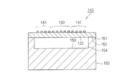
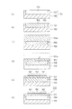
【解決手段】圧電体20の平坦な表面20aからイオンを注入して、圧電体20内において表面20aから所定の深さの領域にイオン注入層22を形成する。圧電体20の表面20aの一部の上に犠牲層30を形成した後、圧電体20の表面20a及び犠牲層30に絶縁体34を形成して圧電構造体10sを形成する。圧電体20を加熱して圧電体20をイオン注入層22で分離して、圧電体20から分離された圧電体膜24と絶縁体34とが接合された圧電体膜構造体10tを形成する。圧電体膜構造体10tの圧電体膜24のイオン注入層22に沿って形成された分割面24aのうち少なくとも犠牲層30に対向する部分に電極を含む素子パターン16を形成した後、圧電体膜構造体10tから犠牲層30を除去する。
【選択図】図3
Description
溶射膜の粒界及び空孔に含浸させて硬化する。これにより、溶射膜の剛性を高めることができるとともに、溶射膜に洗浄液などの不要物が侵入することを防止できる。
10s 圧電構造体
10t 圧電体膜構造体
20 圧電体
20a 表面
22 イオン注入層
24 圧電体膜
24s 第2部分
24t 第1部分
30 犠牲層
32 接着層
34 支持部材(絶縁体)
Claims (13)
- 平坦な表面を有する圧電体を用意する、第1の工程と、
前記圧電体の前記表面からイオンを注入して、前記圧電体内において前記表面から所定の深さの領域にイオン注入層を形成する、第2の工程と、
前記圧電体の前記表面の一部の上に犠牲層を形成する、第3の工程と、
前記圧電体の前記表面及び前記犠牲層に絶縁体を形成して圧電構造体を形成する、第4の工程と、
前記圧電体を加熱して前記圧電体を前記イオン注入層で分離して、前記圧電体から分離された前記圧電体の前記表面と前記イオン注入層との間の圧電体膜と前記絶縁体とが結合された圧電体膜構造体を形成する、第5の工程と、
前記圧電体膜構造体の前記圧電体膜の前記イオン注入層に沿って形成された分割面のうち少なくとも前記犠牲層に対向する部分に電極を形成する、第6の工程と、
前記圧電体膜構造体から前記犠牲層を除去する、第7の工程と、
を備えたことを特徴とする、電子部品の製造方法。 - 前記第4の工程において、
前記圧電体の前記表面及び前記犠牲層の上に、前記圧電体とは反対側に前記圧電体の前記表面よりも粗い表面を有する接着層を形成した後、前記接着層の前記圧電体の前記表面よりも粗い前記表面に前記絶縁体を形成することにより、前記圧電体の前記表面及び前記犠牲層に前記接着層を介して前記絶縁体が形成され前記圧電構造体を形成することを特徴とする、請求項1に記載の電子部品の製造方法。 - 前記接着層がスパッタリング又はCVDにより形成されることを特徴とする、請求項2に記載の電子部品の製造方法。
- 前記接着層は、シリコン酸化膜、シリコン窒化膜、金属酸化膜及び金属窒化膜から選択された少なくとも1種からなることを特徴とする、請求項2又は3に記載の電子部品の製造方法。
- 前記第4の工程において、前記圧電体の前記表面及び前記犠牲層の上に、前記接着層を形成した後に、前記接着層の前記圧電体とは反対側の表面を粗面処理して、前記接着層の前記圧電体の前記表面よりも粗い前記表面を形成することを特徴とする、請求項2乃至4いずれか一項に記載の電子部品の製造方法。
- 前記絶縁体が溶射法により形成されることを特徴とする、請求項1乃至5のいずれか一項に記載の電子部品の製造方法。
- 溶射法により形成された前記絶縁体の粒界及び空孔を充填する工程をさらに有することを特徴とする、請求項6に記載の電子部品の製造方法。
- 前記絶縁体がCVDにより形成されることを特徴とする、請求項1乃至5のいずれか一項に記載の電子部品の製造方法。
- 前記絶縁体がスピン塗布により形成されることを特徴とする、請求項1乃至5のいずれか一項に記載の電子部品の製造方法。
- 前記絶縁体が、SOGをスピン塗布することにより形成されることを特徴とする、請求項9に記載の電子部品の製造方法。
- 支持部材と、
互いに平行な一対の主面を有し、前記支持部材に支持されていない第1部分と前記支持部材に支持された第2部分とを含む圧電体膜と、
前記支持部材と前記圧電体膜の前記第2部分との間に配置され、前記支持部材と前記圧電体膜の前記第2部分とに接している接着層と、
前記圧電体膜の前記第1部分の少なくとも一方の前記主面に形成された電極と、
を備え、
前記接着層は、前記支持部材に接している面の表面粗さが、前記前記圧電体膜の前記第2部分に接している面の表面粗さよりも大きくされていることを特徴とする、電子部品。 - 前記圧電体膜は、一対の前記主面がいずれも鏡面であることを特徴とする、請求項11に記載の電子部品。
- 前記電極により、前記圧電体膜を伝搬する板波が励振されることを特徴とする、請求項11又は12に記載の電子部品。
Priority Applications (3)
| Application Number | Priority Date | Filing Date | Title |
|---|---|---|---|
| JP2008218053A JP4636292B2 (ja) | 2008-08-27 | 2008-08-27 | 電子部品及び電子部品の製造方法 |
| US12/507,284 US8253301B2 (en) | 2008-08-27 | 2009-07-22 | Electronic component and method for manufacturing electronic component |
| US13/556,564 US9015914B2 (en) | 2008-08-27 | 2012-07-24 | Method for manufacturing electronic component |
Applications Claiming Priority (1)
| Application Number | Priority Date | Filing Date | Title |
|---|---|---|---|
| JP2008218053A JP4636292B2 (ja) | 2008-08-27 | 2008-08-27 | 電子部品及び電子部品の製造方法 |
Publications (2)
| Publication Number | Publication Date |
|---|---|
| JP2010056736A true JP2010056736A (ja) | 2010-03-11 |
| JP4636292B2 JP4636292B2 (ja) | 2011-02-23 |
Family
ID=41724264
Family Applications (1)
| Application Number | Title | Priority Date | Filing Date |
|---|---|---|---|
| JP2008218053A Active JP4636292B2 (ja) | 2008-08-27 | 2008-08-27 | 電子部品及び電子部品の製造方法 |
Country Status (2)
| Country | Link |
|---|---|
| US (2) | US8253301B2 (ja) |
| JP (1) | JP4636292B2 (ja) |
Cited By (10)
| Publication number | Priority date | Publication date | Assignee | Title |
|---|---|---|---|---|
| US20100107388A1 (en) * | 2008-10-31 | 2010-05-06 | Murata Manufacturing Co., Ltd. | Method for manufacturing electronic device and method for manufacturing piezoelectric device |
| WO2012073871A1 (ja) * | 2010-11-30 | 2012-06-07 | 株式会社村田製作所 | 弾性波装置及びその製造方法 |
| JP2012199762A (ja) * | 2011-03-22 | 2012-10-18 | Murata Mfg Co Ltd | 圧電デバイスの製造方法 |
| WO2013021948A1 (ja) * | 2011-08-08 | 2013-02-14 | 株式会社村田製作所 | 弾性波装置 |
| JP5152410B2 (ja) * | 2009-06-09 | 2013-02-27 | 株式会社村田製作所 | 圧電デバイスの製造方法 |
| JP2013214954A (ja) * | 2012-03-07 | 2013-10-17 | Taiyo Yuden Co Ltd | 共振子、周波数フィルタ、デュプレクサ、電子機器及び共振子の製造方法 |
| CN103532513A (zh) * | 2012-07-04 | 2014-01-22 | 太阳诱电株式会社 | 兰姆波器件及其制造方法 |
| WO2022102417A1 (ja) * | 2020-11-11 | 2022-05-19 | 株式会社村田製作所 | 弾性波装置 |
| WO2022224973A1 (ja) * | 2021-04-21 | 2022-10-27 | 株式会社村田製作所 | 弾性波装置及び弾性波装置の製造方法 |
| WO2023282264A1 (ja) * | 2021-07-08 | 2023-01-12 | 株式会社村田製作所 | 弾性波装置 |
Families Citing this family (13)
| Publication number | Priority date | Publication date | Assignee | Title |
|---|---|---|---|---|
| WO2011099381A1 (ja) * | 2010-02-09 | 2011-08-18 | 株式会社村田製作所 | 圧電デバイス、圧電デバイスの製造方法 |
| JP5429200B2 (ja) * | 2010-05-17 | 2014-02-26 | 株式会社村田製作所 | 複合圧電基板の製造方法および圧電デバイス |
| US8921165B2 (en) * | 2011-08-03 | 2014-12-30 | Cavendish Kinetics, Inc. | Elimination of silicon residues from MEMS cavity floor |
| US9151153B2 (en) * | 2011-11-30 | 2015-10-06 | Baker Hughes Incorporated | Crystal sensor made by ion implantation for sensing a property of interest within a borehole in the earth |
| US9893264B2 (en) * | 2012-06-15 | 2018-02-13 | Carnegie Mellon University | Method for forming a suspended lithium-based membrane semiconductor structure |
| WO2014027538A1 (ja) * | 2012-08-17 | 2014-02-20 | 日本碍子株式会社 | 複合基板,弾性表面波デバイス及び複合基板の製造方法 |
| US9235937B1 (en) | 2013-06-05 | 2016-01-12 | Analog Devices, Inc. | Mounting method for satellite crash sensors |
| JP5797356B2 (ja) * | 2013-09-26 | 2015-10-21 | 京セラ株式会社 | 弾性波装置および弾性波モジュール |
| CN206878791U (zh) | 2014-12-08 | 2018-01-12 | 株式会社村田制作所 | 压电设备 |
| WO2017052646A1 (en) * | 2015-09-25 | 2017-03-30 | Intel Corporation | Island transfer for optical, piezo and rf applications |
| US11201601B2 (en) * | 2018-06-15 | 2021-12-14 | Resonant Inc. | Transversely-excited film bulk acoustic resonator with multiple diaphragm thicknesses and fabrication method |
| JP2020161899A (ja) * | 2019-03-25 | 2020-10-01 | 太陽誘電株式会社 | 弾性波デバイス、フィルタおよびマルチプレクサ |
| CN114553163B (zh) * | 2022-04-28 | 2022-09-06 | 深圳新声半导体有限公司 | 体声波谐振器的制造方法 |
Citations (7)
| Publication number | Priority date | Publication date | Assignee | Title |
|---|---|---|---|---|
| JP2002016466A (ja) * | 2000-06-30 | 2002-01-18 | Kyocera Corp | 弾性表面波装置及びその製造方法 |
| JP2002534886A (ja) * | 1998-12-30 | 2002-10-15 | タレス | 分子結合剤によってキャリヤ基板に結合された圧電材料の薄層中で案内される表面弾性波のためのデバイスおよび製造方法 |
| JP2003017967A (ja) * | 2001-06-29 | 2003-01-17 | Toshiba Corp | 弾性表面波素子及びその製造方法 |
| JP2005342817A (ja) * | 2004-06-01 | 2005-12-15 | Sony Corp | 中空構造素子およびその製造方法ならびに電子機器 |
| JP2006186900A (ja) * | 2004-12-28 | 2006-07-13 | Seiko Epson Corp | 弾性表面波素子複合装置 |
| JP2007251910A (ja) * | 2006-02-16 | 2007-09-27 | Seiko Epson Corp | ラム波型高周波デバイス、ラム波型高周波デバイスの製造方法 |
| WO2009081651A1 (ja) * | 2007-12-25 | 2009-07-02 | Murata Manufacturing Co., Ltd. | 複合圧電基板の製造方法 |
Family Cites Families (14)
| Publication number | Priority date | Publication date | Assignee | Title |
|---|---|---|---|---|
| JPH04102314A (ja) * | 1990-08-21 | 1992-04-03 | Fujitsu Ltd | 半導体装置の製造方法 |
| JP3940804B2 (ja) | 1997-09-04 | 2007-07-04 | 株式会社ニコン | ハイブリッド型半導体装置及びその製造方法 |
| US6120597A (en) | 1998-02-17 | 2000-09-19 | The Trustees Of Columbia University In The City Of New York | Crystal ion-slicing of single-crystal films |
| US6355498B1 (en) * | 2000-08-11 | 2002-03-12 | Agere Systems Guartian Corp. | Thin film resonators fabricated on membranes created by front side releasing |
| US20040224482A1 (en) * | 2001-12-20 | 2004-11-11 | Kub Francis J. | Method for transferring thin film layer material to a flexible substrate using a hydrogen ion splitting technique |
| ES2599061T3 (es) * | 2002-12-02 | 2017-01-31 | Avery Dennison Corporation | Etiqueta de transferencia por calor |
| KR100489828B1 (ko) | 2003-04-07 | 2005-05-16 | 삼성전기주식회사 | Fbar 소자 및 그 제조방법 |
| US7299529B2 (en) * | 2005-06-16 | 2007-11-27 | Intel Corporation | Film bulk acoustic resonator (FBAR) process using single-step resonator layer deposition |
| JP4793568B2 (ja) * | 2005-07-08 | 2011-10-12 | セイコーエプソン株式会社 | アクチュエータ装置、液体噴射ヘッド及び液体噴射装置 |
| US7479685B2 (en) * | 2006-03-10 | 2009-01-20 | Avago Technologies General Ip (Singapore) Pte. Ltd. | Electronic device on substrate with cavity and mitigated parasitic leakage path |
| US7569976B2 (en) * | 2006-07-27 | 2009-08-04 | Koike Co., Ltd. | Piezo-electric substrate and manufacturing method of the same |
| JP4247281B2 (ja) | 2006-07-27 | 2009-04-02 | 株式会社コイケ | 圧電基板及びその製造方法 |
| WO2010067794A1 (ja) * | 2008-12-10 | 2010-06-17 | 株式会社村田製作所 | 圧電性複合基板の製造方法、および圧電素子の製造方法 |
| JP5796316B2 (ja) * | 2011-03-22 | 2015-10-21 | 株式会社村田製作所 | 圧電デバイスの製造方法 |
-
2008
- 2008-08-27 JP JP2008218053A patent/JP4636292B2/ja active Active
-
2009
- 2009-07-22 US US12/507,284 patent/US8253301B2/en active Active
-
2012
- 2012-07-24 US US13/556,564 patent/US9015914B2/en active Active
Patent Citations (7)
| Publication number | Priority date | Publication date | Assignee | Title |
|---|---|---|---|---|
| JP2002534886A (ja) * | 1998-12-30 | 2002-10-15 | タレス | 分子結合剤によってキャリヤ基板に結合された圧電材料の薄層中で案内される表面弾性波のためのデバイスおよび製造方法 |
| JP2002016466A (ja) * | 2000-06-30 | 2002-01-18 | Kyocera Corp | 弾性表面波装置及びその製造方法 |
| JP2003017967A (ja) * | 2001-06-29 | 2003-01-17 | Toshiba Corp | 弾性表面波素子及びその製造方法 |
| JP2005342817A (ja) * | 2004-06-01 | 2005-12-15 | Sony Corp | 中空構造素子およびその製造方法ならびに電子機器 |
| JP2006186900A (ja) * | 2004-12-28 | 2006-07-13 | Seiko Epson Corp | 弾性表面波素子複合装置 |
| JP2007251910A (ja) * | 2006-02-16 | 2007-09-27 | Seiko Epson Corp | ラム波型高周波デバイス、ラム波型高周波デバイスの製造方法 |
| WO2009081651A1 (ja) * | 2007-12-25 | 2009-07-02 | Murata Manufacturing Co., Ltd. | 複合圧電基板の製造方法 |
Cited By (16)
| Publication number | Priority date | Publication date | Assignee | Title |
|---|---|---|---|---|
| US9240543B2 (en) * | 2008-10-31 | 2016-01-19 | Murata Manufacturing Co., Ltd. | Method for manufacturing piezoelectric device |
| US20100107388A1 (en) * | 2008-10-31 | 2010-05-06 | Murata Manufacturing Co., Ltd. | Method for manufacturing electronic device and method for manufacturing piezoelectric device |
| JP5152410B2 (ja) * | 2009-06-09 | 2013-02-27 | 株式会社村田製作所 | 圧電デバイスの製造方法 |
| JP5601377B2 (ja) * | 2010-11-30 | 2014-10-08 | 株式会社村田製作所 | 弾性波装置及びその製造方法 |
| WO2012073871A1 (ja) * | 2010-11-30 | 2012-06-07 | 株式会社村田製作所 | 弾性波装置及びその製造方法 |
| US9748923B2 (en) | 2010-11-30 | 2017-08-29 | Murata Manufacturing Co., Ltd. | Elastic wave device and manufacturing method for same |
| JP2012199762A (ja) * | 2011-03-22 | 2012-10-18 | Murata Mfg Co Ltd | 圧電デバイスの製造方法 |
| WO2013021948A1 (ja) * | 2011-08-08 | 2013-02-14 | 株式会社村田製作所 | 弾性波装置 |
| JPWO2013021948A1 (ja) * | 2011-08-08 | 2015-03-05 | 株式会社村田製作所 | 弾性波装置 |
| US9564873B2 (en) | 2011-08-08 | 2017-02-07 | Murata Manufacturing Co., Ltd. | Elastic wave device |
| JP2013214954A (ja) * | 2012-03-07 | 2013-10-17 | Taiyo Yuden Co Ltd | 共振子、周波数フィルタ、デュプレクサ、電子機器及び共振子の製造方法 |
| CN103532513A (zh) * | 2012-07-04 | 2014-01-22 | 太阳诱电株式会社 | 兰姆波器件及其制造方法 |
| JP2014013991A (ja) * | 2012-07-04 | 2014-01-23 | Taiyo Yuden Co Ltd | ラム波デバイスおよびその製造方法 |
| WO2022102417A1 (ja) * | 2020-11-11 | 2022-05-19 | 株式会社村田製作所 | 弾性波装置 |
| WO2022224973A1 (ja) * | 2021-04-21 | 2022-10-27 | 株式会社村田製作所 | 弾性波装置及び弾性波装置の製造方法 |
| WO2023282264A1 (ja) * | 2021-07-08 | 2023-01-12 | 株式会社村田製作所 | 弾性波装置 |
Also Published As
| Publication number | Publication date |
|---|---|
| US9015914B2 (en) | 2015-04-28 |
| JP4636292B2 (ja) | 2011-02-23 |
| US20120284979A1 (en) | 2012-11-15 |
| US8253301B2 (en) | 2012-08-28 |
| US20100052472A1 (en) | 2010-03-04 |
Similar Documents
| Publication | Publication Date | Title |
|---|---|---|
| JP4636292B2 (ja) | 電子部品及び電子部品の製造方法 | |
| JP4345049B2 (ja) | 薄膜音響共振器及びその製造方法 | |
| CN101908865B (zh) | 体波谐振器及其加工方法 | |
| US8872409B2 (en) | Method for manufacturing composite piezoelectric substrate and piezoelectric device | |
| JP4627269B2 (ja) | 圧電薄膜デバイスの製造方法 | |
| JP2007028669A (ja) | 薄膜音響共振器の製造方法 | |
| JP2007228356A (ja) | 圧電薄膜デバイス | |
| US8431031B2 (en) | Method for producing a bulk wave acoustic resonator of FBAR type | |
| WO2005060091A1 (ja) | 圧電薄膜デバイスの製造方法および圧電薄膜デバイス | |
| JP2003017967A (ja) | 弾性表面波素子及びその製造方法 | |
| JP5817830B2 (ja) | 圧電バルク波装置及びその製造方法 | |
| JP4395892B2 (ja) | 圧電薄膜デバイス及びその製造方法 | |
| US8764998B2 (en) | Method for manufacturing composite substrate | |
| JP2007228341A (ja) | 圧電薄膜デバイス | |
| CN111030628A (zh) | 一种体声波谐振器的制备方法 | |
| CN117118388B (zh) | 一种多层复合晶圆及薄膜弹性波器件 | |
| JP5862368B2 (ja) | 圧電デバイスの製造方法 | |
| JP5277999B2 (ja) | 複合基板の製造方法 | |
| JP2009089006A (ja) | 圧電薄膜振動子の製造方法及び圧電薄膜振動子 | |
| JP4730383B2 (ja) | 薄膜音響共振器及びその製造方法 | |
| JP2010166203A (ja) | 複合基板の製造方法 | |
| JP2005303573A (ja) | 薄膜圧電共振器及びその製造方法 | |
| JP2003318695A (ja) | 圧電薄膜共振子およびその製造方法 | |
| JP2007228340A (ja) | 圧電薄膜デバイス | |
| JP3918464B2 (ja) | 薄膜音響共振器及びその製造方法 |
Legal Events
| Date | Code | Title | Description |
|---|---|---|---|
| A621 | Written request for application examination |
Free format text: JAPANESE INTERMEDIATE CODE: A621 Effective date: 20100201 |
|
| A977 | Report on retrieval |
Free format text: JAPANESE INTERMEDIATE CODE: A971007 Effective date: 20100610 |
|
| A131 | Notification of reasons for refusal |
Free format text: JAPANESE INTERMEDIATE CODE: A131 Effective date: 20100624 |
|
| A521 | Request for written amendment filed |
Free format text: JAPANESE INTERMEDIATE CODE: A523 Effective date: 20100818 |
|
| TRDD | Decision of grant or rejection written | ||
| A01 | Written decision to grant a patent or to grant a registration (utility model) |
Free format text: JAPANESE INTERMEDIATE CODE: A01 Effective date: 20101027 |
|
| A01 | Written decision to grant a patent or to grant a registration (utility model) |
Free format text: JAPANESE INTERMEDIATE CODE: A01 |
|
| A61 | First payment of annual fees (during grant procedure) |
Free format text: JAPANESE INTERMEDIATE CODE: A61 Effective date: 20101109 |
|
| FPAY | Renewal fee payment (event date is renewal date of database) |
Free format text: PAYMENT UNTIL: 20131203 Year of fee payment: 3 |
|
| R150 | Certificate of patent or registration of utility model |
Ref document number: 4636292 Country of ref document: JP Free format text: JAPANESE INTERMEDIATE CODE: R150 Free format text: JAPANESE INTERMEDIATE CODE: R150 |