US11374549B2 - Filter using transversely-excited film bulk acoustic resonators with divided frequency-setting dielectric layers - Google Patents
Filter using transversely-excited film bulk acoustic resonators with divided frequency-setting dielectric layers Download PDFInfo
- Publication number
- US11374549B2 US11374549B2 US17/081,717 US202017081717A US11374549B2 US 11374549 B2 US11374549 B2 US 11374549B2 US 202017081717 A US202017081717 A US 202017081717A US 11374549 B2 US11374549 B2 US 11374549B2
- Authority
- US
- United States
- Prior art keywords
- frequency setting
- setting layer
- side frequency
- resonators
- thickness
- Prior art date
- Legal status (The legal status is an assumption and is not a legal conclusion. Google has not performed a legal analysis and makes no representation as to the accuracy of the status listed.)
- Active, expires
Links
- 239000000758 substrate Substances 0.000 claims abstract description 54
- 239000013078 crystal Substances 0.000 claims abstract description 5
- 239000000463 material Substances 0.000 claims description 24
- VYPSYNLAJGMNEJ-UHFFFAOYSA-N Silicium dioxide Chemical compound O=[Si]=O VYPSYNLAJGMNEJ-UHFFFAOYSA-N 0.000 claims description 23
- 239000003989 dielectric material Substances 0.000 claims description 17
- 239000000377 silicon dioxide Substances 0.000 claims description 11
- 235000012239 silicon dioxide Nutrition 0.000 claims description 6
- 229910052581 Si3N4 Inorganic materials 0.000 claims description 5
- PMHQVHHXPFUNSP-UHFFFAOYSA-M copper(1+);methylsulfanylmethane;bromide Chemical compound Br[Cu].CSC PMHQVHHXPFUNSP-UHFFFAOYSA-M 0.000 claims description 5
- 238000002161 passivation Methods 0.000 claims description 5
- HQVNEWCFYHHQES-UHFFFAOYSA-N silicon nitride Chemical compound N12[Si]34N5[Si]62N3[Si]51N64 HQVNEWCFYHHQES-UHFFFAOYSA-N 0.000 claims description 5
- FRWYFWZENXDZMU-UHFFFAOYSA-N 2-iodoquinoline Chemical compound C1=CC=CC2=NC(I)=CC=C21 FRWYFWZENXDZMU-UHFFFAOYSA-N 0.000 claims description 4
- LTPBRCUWZOMYOC-UHFFFAOYSA-N beryllium oxide Inorganic materials O=[Be] LTPBRCUWZOMYOC-UHFFFAOYSA-N 0.000 claims description 4
- QGLKJKCYBOYXKC-UHFFFAOYSA-N nonaoxidotritungsten Chemical compound O=[W]1(=O)O[W](=O)(=O)O[W](=O)(=O)O1 QGLKJKCYBOYXKC-UHFFFAOYSA-N 0.000 claims description 4
- TWNQGVIAIRXVLR-UHFFFAOYSA-N oxo(oxoalumanyloxy)alumane Chemical compound O=[Al]O[Al]=O TWNQGVIAIRXVLR-UHFFFAOYSA-N 0.000 claims description 4
- BPUBBGLMJRNUCC-UHFFFAOYSA-N oxygen(2-);tantalum(5+) Chemical compound [O-2].[O-2].[O-2].[O-2].[O-2].[Ta+5].[Ta+5] BPUBBGLMJRNUCC-UHFFFAOYSA-N 0.000 claims description 4
- 229910001936 tantalum oxide Inorganic materials 0.000 claims description 4
- 229910001930 tungsten oxide Inorganic materials 0.000 claims description 4
- 238000000034 method Methods 0.000 abstract description 22
- 238000004519 manufacturing process Methods 0.000 abstract description 3
- 239000004020 conductor Substances 0.000 description 22
- 230000008569 process Effects 0.000 description 15
- 238000004891 communication Methods 0.000 description 14
- 230000008878 coupling Effects 0.000 description 9
- 238000010168 coupling process Methods 0.000 description 9
- 238000005859 coupling reaction Methods 0.000 description 9
- 238000005530 etching Methods 0.000 description 9
- 239000010408 film Substances 0.000 description 9
- 238000000151 deposition Methods 0.000 description 8
- 229910052751 metal Inorganic materials 0.000 description 8
- 230000005684 electric field Effects 0.000 description 7
- 239000002184 metal Substances 0.000 description 7
- 229910052681 coesite Inorganic materials 0.000 description 6
- 229910052906 cristobalite Inorganic materials 0.000 description 6
- 229910052682 stishovite Inorganic materials 0.000 description 6
- 238000010897 surface acoustic wave method Methods 0.000 description 6
- 229910052905 tridymite Inorganic materials 0.000 description 6
- 229910052782 aluminium Inorganic materials 0.000 description 5
- XAGFODPZIPBFFR-UHFFFAOYSA-N aluminium Chemical compound [Al] XAGFODPZIPBFFR-UHFFFAOYSA-N 0.000 description 5
- 230000013011 mating Effects 0.000 description 5
- RTAQQCXQSZGOHL-UHFFFAOYSA-N Titanium Chemical compound [Ti] RTAQQCXQSZGOHL-UHFFFAOYSA-N 0.000 description 4
- GQYHUHYESMUTHG-UHFFFAOYSA-N lithium niobate Chemical compound [Li+].[O-][Nb](=O)=O GQYHUHYESMUTHG-UHFFFAOYSA-N 0.000 description 4
- 230000033001 locomotion Effects 0.000 description 4
- 239000007787 solid Substances 0.000 description 4
- 229910052719 titanium Inorganic materials 0.000 description 4
- 239000010936 titanium Substances 0.000 description 4
- WSMQKESQZFQMFW-UHFFFAOYSA-N 5-methyl-pyrazole-3-carboxylic acid Chemical compound CC1=CC(C(O)=O)=NN1 WSMQKESQZFQMFW-UHFFFAOYSA-N 0.000 description 3
- RYGMFSIKBFXOCR-UHFFFAOYSA-N Copper Chemical compound [Cu] RYGMFSIKBFXOCR-UHFFFAOYSA-N 0.000 description 3
- XUIMIQQOPSSXEZ-UHFFFAOYSA-N Silicon Chemical compound [Si] XUIMIQQOPSSXEZ-UHFFFAOYSA-N 0.000 description 3
- 230000009471 action Effects 0.000 description 3
- 239000002131 composite material Substances 0.000 description 3
- 238000010276 construction Methods 0.000 description 3
- 229910052802 copper Inorganic materials 0.000 description 3
- 239000010949 copper Substances 0.000 description 3
- 238000013461 design Methods 0.000 description 3
- 238000005516 engineering process Methods 0.000 description 3
- 229920002120 photoresistant polymer Polymers 0.000 description 3
- 229910052710 silicon Inorganic materials 0.000 description 3
- 239000010703 silicon Substances 0.000 description 3
- 229910000838 Al alloy Inorganic materials 0.000 description 2
- VYZAMTAEIAYCRO-UHFFFAOYSA-N Chromium Chemical compound [Cr] VYZAMTAEIAYCRO-UHFFFAOYSA-N 0.000 description 2
- 229910000881 Cu alloy Inorganic materials 0.000 description 2
- 230000008021 deposition Effects 0.000 description 2
- 238000010586 diagram Methods 0.000 description 2
- 230000000694 effects Effects 0.000 description 2
- 230000005284 excitation Effects 0.000 description 2
- PCHJSUWPFVWCPO-UHFFFAOYSA-N gold Chemical compound [Au] PCHJSUWPFVWCPO-UHFFFAOYSA-N 0.000 description 2
- 229910052737 gold Inorganic materials 0.000 description 2
- 239000010931 gold Substances 0.000 description 2
- 238000003780 insertion Methods 0.000 description 2
- 230000037431 insertion Effects 0.000 description 2
- 238000001020 plasma etching Methods 0.000 description 2
- 238000004088 simulation Methods 0.000 description 2
- 238000012360 testing method Methods 0.000 description 2
- 239000010409 thin film Substances 0.000 description 2
- 229910002601 GaN Inorganic materials 0.000 description 1
- GYHNNYVSQQEPJS-UHFFFAOYSA-N Gallium Chemical compound [Ga] GYHNNYVSQQEPJS-UHFFFAOYSA-N 0.000 description 1
- JMASRVWKEDWRBT-UHFFFAOYSA-N Gallium nitride Chemical compound [Ga]#N JMASRVWKEDWRBT-UHFFFAOYSA-N 0.000 description 1
- 235000019687 Lamb Nutrition 0.000 description 1
- ZOKXTWBITQBERF-UHFFFAOYSA-N Molybdenum Chemical compound [Mo] ZOKXTWBITQBERF-UHFFFAOYSA-N 0.000 description 1
- BPQQTUXANYXVAA-UHFFFAOYSA-N Orthosilicate Chemical compound [O-][Si]([O-])([O-])[O-] BPQQTUXANYXVAA-UHFFFAOYSA-N 0.000 description 1
- 229910005171 Si3O4 Inorganic materials 0.000 description 1
- 230000002411 adverse Effects 0.000 description 1
- 238000000137 annealing Methods 0.000 description 1
- 230000008901 benefit Effects 0.000 description 1
- 229910052790 beryllium Inorganic materials 0.000 description 1
- ATBAMAFKBVZNFJ-UHFFFAOYSA-N beryllium atom Chemical compound [Be] ATBAMAFKBVZNFJ-UHFFFAOYSA-N 0.000 description 1
- 230000002457 bidirectional effect Effects 0.000 description 1
- 230000005540 biological transmission Effects 0.000 description 1
- 230000015572 biosynthetic process Effects 0.000 description 1
- 230000001413 cellular effect Effects 0.000 description 1
- 238000005229 chemical vapour deposition Methods 0.000 description 1
- 229910052804 chromium Inorganic materials 0.000 description 1
- 239000011651 chromium Substances 0.000 description 1
- -1 chromium or titanium Chemical class 0.000 description 1
- 238000004140 cleaning Methods 0.000 description 1
- 230000001419 dependent effect Effects 0.000 description 1
- 238000003870 depth resolved spectroscopy Methods 0.000 description 1
- 208000009743 drug hypersensitivity syndrome Diseases 0.000 description 1
- 238000005538 encapsulation Methods 0.000 description 1
- 238000001704 evaporation Methods 0.000 description 1
- 230000008020 evaporation Effects 0.000 description 1
- 229910052733 gallium Inorganic materials 0.000 description 1
- 238000007689 inspection Methods 0.000 description 1
- 230000001788 irregular Effects 0.000 description 1
- 238000002955 isolation Methods 0.000 description 1
- 229910052746 lanthanum Inorganic materials 0.000 description 1
- FZLIPJUXYLNCLC-UHFFFAOYSA-N lanthanum atom Chemical compound [La] FZLIPJUXYLNCLC-UHFFFAOYSA-N 0.000 description 1
- 238000001459 lithography Methods 0.000 description 1
- 239000007769 metal material Substances 0.000 description 1
- 150000002739 metals Chemical class 0.000 description 1
- 230000000116 mitigating effect Effects 0.000 description 1
- 229910052750 molybdenum Inorganic materials 0.000 description 1
- 239000011733 molybdenum Substances 0.000 description 1
- 238000012544 monitoring process Methods 0.000 description 1
- 238000004806 packaging method and process Methods 0.000 description 1
- 238000000059 patterning Methods 0.000 description 1
- 238000000206 photolithography Methods 0.000 description 1
- 238000002360 preparation method Methods 0.000 description 1
- 238000012545 processing Methods 0.000 description 1
- 239000010453 quartz Substances 0.000 description 1
- 230000009467 reduction Effects 0.000 description 1
- 229910052594 sapphire Inorganic materials 0.000 description 1
- 239000010980 sapphire Substances 0.000 description 1
- 238000000926 separation method Methods 0.000 description 1
- 239000004432 silane-modified polyurethane Substances 0.000 description 1
- 229910000679 solder Inorganic materials 0.000 description 1
- 238000004544 sputter deposition Methods 0.000 description 1
- 238000012546 transfer Methods 0.000 description 1
- 238000012800 visualization Methods 0.000 description 1
- 238000003631 wet chemical etching Methods 0.000 description 1
Images


Classifications
-
- H—ELECTRICITY
- H03—ELECTRONIC CIRCUITRY
- H03H—IMPEDANCE NETWORKS, e.g. RESONANT CIRCUITS; RESONATORS
- H03H3/00—Apparatus or processes specially adapted for the manufacture of impedance networks, resonating circuits, resonators
- H03H3/007—Apparatus or processes specially adapted for the manufacture of impedance networks, resonating circuits, resonators for the manufacture of electromechanical resonators or networks
- H03H3/02—Apparatus or processes specially adapted for the manufacture of impedance networks, resonating circuits, resonators for the manufacture of electromechanical resonators or networks for the manufacture of piezoelectric or electrostrictive resonators or networks
- H03H3/04—Apparatus or processes specially adapted for the manufacture of impedance networks, resonating circuits, resonators for the manufacture of electromechanical resonators or networks for the manufacture of piezoelectric or electrostrictive resonators or networks for obtaining desired frequency or temperature coefficient
-
- H—ELECTRICITY
- H03—ELECTRONIC CIRCUITRY
- H03H—IMPEDANCE NETWORKS, e.g. RESONANT CIRCUITS; RESONATORS
- H03H9/00—Networks comprising electromechanical or electro-acoustic devices; Electromechanical resonators
- H03H9/02—Details
- H03H9/02007—Details of bulk acoustic wave devices
- H03H9/02015—Characteristics of piezoelectric layers, e.g. cutting angles
- H03H9/02031—Characteristics of piezoelectric layers, e.g. cutting angles consisting of ceramic
-
- H—ELECTRICITY
- H03—ELECTRONIC CIRCUITRY
- H03H—IMPEDANCE NETWORKS, e.g. RESONANT CIRCUITS; RESONATORS
- H03H9/00—Networks comprising electromechanical or electro-acoustic devices; Electromechanical resonators
- H03H9/02—Details
- H03H9/02228—Guided bulk acoustic wave devices or Lamb wave devices having interdigital transducers situated in parallel planes on either side of a piezoelectric layer
-
- H—ELECTRICITY
- H03—ELECTRONIC CIRCUITRY
- H03H—IMPEDANCE NETWORKS, e.g. RESONANT CIRCUITS; RESONATORS
- H03H9/00—Networks comprising electromechanical or electro-acoustic devices; Electromechanical resonators
- H03H9/02—Details
- H03H9/125—Driving means, e.g. electrodes, coils
- H03H9/13—Driving means, e.g. electrodes, coils for networks consisting of piezoelectric or electrostrictive materials
- H03H9/132—Driving means, e.g. electrodes, coils for networks consisting of piezoelectric or electrostrictive materials characterized by a particular shape
-
- H—ELECTRICITY
- H03—ELECTRONIC CIRCUITRY
- H03H—IMPEDANCE NETWORKS, e.g. RESONANT CIRCUITS; RESONATORS
- H03H9/00—Networks comprising electromechanical or electro-acoustic devices; Electromechanical resonators
- H03H9/15—Constructional features of resonators consisting of piezoelectric or electrostrictive material
- H03H9/17—Constructional features of resonators consisting of piezoelectric or electrostrictive material having a single resonator
- H03H9/171—Constructional features of resonators consisting of piezoelectric or electrostrictive material having a single resonator implemented with thin-film techniques, i.e. of the film bulk acoustic resonator [FBAR] type
- H03H9/172—Means for mounting on a substrate, i.e. means constituting the material interface confining the waves to a volume
- H03H9/174—Membranes
-
- H—ELECTRICITY
- H03—ELECTRONIC CIRCUITRY
- H03H—IMPEDANCE NETWORKS, e.g. RESONANT CIRCUITS; RESONATORS
- H03H9/00—Networks comprising electromechanical or electro-acoustic devices; Electromechanical resonators
- H03H9/15—Constructional features of resonators consisting of piezoelectric or electrostrictive material
- H03H9/17—Constructional features of resonators consisting of piezoelectric or electrostrictive material having a single resonator
- H03H9/176—Constructional features of resonators consisting of piezoelectric or electrostrictive material having a single resonator consisting of ceramic material
-
- H—ELECTRICITY
- H03—ELECTRONIC CIRCUITRY
- H03H—IMPEDANCE NETWORKS, e.g. RESONANT CIRCUITS; RESONATORS
- H03H9/00—Networks comprising electromechanical or electro-acoustic devices; Electromechanical resonators
- H03H9/46—Filters
- H03H9/54—Filters comprising resonators of piezo-electric or electrostrictive material
- H03H9/56—Monolithic crystal filters
- H03H9/562—Monolithic crystal filters comprising a ceramic piezoelectric layer
-
- H—ELECTRICITY
- H03—ELECTRONIC CIRCUITRY
- H03H—IMPEDANCE NETWORKS, e.g. RESONANT CIRCUITS; RESONATORS
- H03H9/00—Networks comprising electromechanical or electro-acoustic devices; Electromechanical resonators
- H03H9/46—Filters
- H03H9/54—Filters comprising resonators of piezo-electric or electrostrictive material
- H03H9/56—Monolithic crystal filters
- H03H9/564—Monolithic crystal filters implemented with thin-film techniques
-
- H—ELECTRICITY
- H03—ELECTRONIC CIRCUITRY
- H03H—IMPEDANCE NETWORKS, e.g. RESONANT CIRCUITS; RESONATORS
- H03H9/00—Networks comprising electromechanical or electro-acoustic devices; Electromechanical resonators
- H03H9/46—Filters
- H03H9/54—Filters comprising resonators of piezo-electric or electrostrictive material
- H03H9/56—Monolithic crystal filters
- H03H9/566—Electric coupling means therefor
- H03H9/568—Electric coupling means therefor consisting of a ladder configuration
-
- H—ELECTRICITY
- H03—ELECTRONIC CIRCUITRY
- H03H—IMPEDANCE NETWORKS, e.g. RESONANT CIRCUITS; RESONATORS
- H03H3/00—Apparatus or processes specially adapted for the manufacture of impedance networks, resonating circuits, resonators
- H03H3/007—Apparatus or processes specially adapted for the manufacture of impedance networks, resonating circuits, resonators for the manufacture of electromechanical resonators or networks
- H03H3/02—Apparatus or processes specially adapted for the manufacture of impedance networks, resonating circuits, resonators for the manufacture of electromechanical resonators or networks for the manufacture of piezoelectric or electrostrictive resonators or networks
- H03H2003/023—Apparatus or processes specially adapted for the manufacture of impedance networks, resonating circuits, resonators for the manufacture of electromechanical resonators or networks for the manufacture of piezoelectric or electrostrictive resonators or networks the resonators or networks being of the membrane type
-
- H—ELECTRICITY
- H03—ELECTRONIC CIRCUITRY
- H03H—IMPEDANCE NETWORKS, e.g. RESONANT CIRCUITS; RESONATORS
- H03H3/00—Apparatus or processes specially adapted for the manufacture of impedance networks, resonating circuits, resonators
- H03H3/007—Apparatus or processes specially adapted for the manufacture of impedance networks, resonating circuits, resonators for the manufacture of electromechanical resonators or networks
- H03H3/02—Apparatus or processes specially adapted for the manufacture of impedance networks, resonating circuits, resonators for the manufacture of electromechanical resonators or networks for the manufacture of piezoelectric or electrostrictive resonators or networks
- H03H3/04—Apparatus or processes specially adapted for the manufacture of impedance networks, resonating circuits, resonators for the manufacture of electromechanical resonators or networks for the manufacture of piezoelectric or electrostrictive resonators or networks for obtaining desired frequency or temperature coefficient
- H03H2003/0414—Resonance frequency
- H03H2003/0421—Modification of the thickness of an element
- H03H2003/0442—Modification of the thickness of an element of a non-piezoelectric layer
Definitions
- This disclosure relates to radio frequency filters using acoustic wave resonators, and specifically to filters for use in communications equipment.
- a radio frequency (RF) filter is a two-port device configured to pass some frequencies and to stop other frequencies, where “pass” means transmit with relatively low signal loss and “stop” means block or substantially attenuate.
- the range of frequencies passed by a filter is referred to as the “pass-band” of the filter.
- the range of frequencies stopped by such a filter is referred to as the “stop-band” of the filter.
- a typical RF filter has at least one pass-band and at least one stop-band. Specific requirements on a passband or stop-band depend on the specific application.
- a “pass-band” may be defined as a frequency range where the insertion loss of a filter is better than a defined value such as 1 dB, 2 dB, or 3 dB.
- a “stop-band” may be defined as a frequency range where the rejection of a filter is greater than a defined value such as 20 dB, 30 dB, 40 dB, or greater depending on application.
- RF filters are used in communications systems where information is transmitted over wireless links.
- RF filters may be found in the RF front-ends of cellular base stations, mobile telephone and computing devices, satellite transceivers and ground stations, IoT (Internet of Things) devices, laptop computers and tablets, fixed point radio links, and other communications systems.
- IoT Internet of Things
- RF filters are also used in radar and electronic and information warfare systems.
- RF filters typically require many design trade-offs to achieve, for each specific application, the best compromise between performance parameters such as insertion loss, rejection, isolation, power handling, linearity, size and cost. Specific design and manufacturing methods and enhancements can benefit simultaneously one or several of these requirements.
- Performance enhancements to the RF filters in a wireless system can have broad impact to system performance. Improvements in RF filters can be leveraged to provide system performance improvements such as larger cell size, longer battery life, higher data rates, greater network capacity, lower cost, enhanced security, higher reliability, etc. These improvements can be realized at many levels of the wireless system both separately and in combination, for example at the RF module, RF transceiver, mobile or fixed sub-system, or network levels.
- High performance RF filters for present communication systems commonly incorporate acoustic wave resonators including surface acoustic wave (SAW) resonators, bulk acoustic wave (BAW) resonators, film bulk acoustic wave resonators (FBAR), and other types of acoustic resonators.
- SAW surface acoustic wave
- BAW bulk acoustic wave
- FBAR film bulk acoustic wave resonators
- these existing technologies are not well-suited for use at the higher frequencies proposed for future communications networks.
- Radio access technology for mobile telephone networks has been standardized by the 3GPP (3 rd Generation Partnership Project).
- Radio access technology for 5 th generation mobile networks is defined in the 5G NR (new radio) standard.
- the 5G NR standard defines several new communications bands. Two of these new communications bands are n77, which uses the frequency range from 3300 MHz to 4200 MHz, and n79, which uses the frequency range from 4400 MHz to 5000 MHz. Both band n77 and band n79 use time-division duplexing (TDD), such that a communications device operating in band n77 and/or band n79 use the same frequencies for both uplink and downlink transmissions. Bandpass filters for bands n77 and n79 must be capable of handling the transmit power of the communications device.
- the 5G NR standard also defines millimeter wave communication bands with frequencies between 24.25 GHz and 40 GHz.
- FIG. 1 is a schematic plan view and two schematic cross-sectional views of a transversely-excited film bulk acoustic resonator (XBAR).
- XBAR transversely-excited film bulk acoustic resonator
- FIG. 2 is an expanded schematic cross-sectional view of a portion of the XBAR of FIG. 1 .
- FIG. 3 is an alternative schematic cross-sectional view of the XBAR of FIG. 1 .
- FIG. 4 is a graphic illustrating a shear primary acoustic mode in an XBAR.
- FIG. 5 is a schematic block diagram of a filter using XBARs.
- FIG. 6 is a schematic cross-sectional view of two XBARs illustrating a frequency-setting dielectric layer.
- FIG. 7 is a graph of the admittance of an XBAR with a thick frequency-setting dielectric layer.
- FIG. 8 is a schematic cross-sectional view of two XBARs illustrating divided frequency-setting dielectric layers.
- FIG. 9 is a graph of the admittance of an XBAR with a divided frequency-setting dielectric layer.
- FIG. 10 is a graph of the admittance of another XBAR with a divided frequency-setting dielectric layer.
- FIG. 11 is a graph of the admittance of another XBAR with a divided frequency-setting dielectric layer.
- FIG. 12 is a graph of the effects of back-side frequency setting layer thickness on XBAR performance.
- FIG. 13 is a flow chart of a process for fabricating XBARs.
- FIG. 1 shows a simplified schematic top view and orthogonal cross-sectional views of a transversely-excited film bulk acoustic resonator (XBAR) 100 .
- XBAR resonators such as the resonator 100 may be used in a variety of RF filters including band-reject filters, band-pass filters, duplexers, and multiplexers.
- XBARs are well suited for use in filters for communications bands with frequencies above 3 GHz.
- the XBAR 100 is made up of a thin film conductor pattern formed on a surface of a piezoelectric plate 110 having a front surface 112 and a back surface 114 .
- the front and back surfaces are essentially parallel. “Essentially parallel” means parallel to the extent possible within normal manufacturing tolerances.
- the piezoelectric plate is a thin single-crystal layer of a piezoelectric material such as lithium niobate, lithium tantalate, lanthanum gallium silicate, gallium nitride, or aluminum nitride. The piezoelectric plate is cut such that the orientation of the X, Y, and Z crystalline axes with respect to the front and back surfaces is known and consistent.
- the piezoelectric plates are Z-cut, which is to say the Z axis is normal to the front surface 112 and back surface 114 .
- XBARs may be fabricated on piezoelectric plates with other crystallographic orientations including rotated Z-cut and rotated YX-cut.
- the back surface 114 of the piezoelectric plate 110 is attached to a surface 122 of the substrate 120 except for a portion of the piezoelectric plate 110 that forms a diaphragm 115 spanning a cavity 140 formed in the substrate 120 .
- the portion of the piezoelectric plate that spans the cavity is referred to herein as the “diaphragm” due to its physical resemblance to the diaphragm of a microphone.
- the diaphragm 115 is contiguous with the rest of the piezoelectric plate 110 around all of a perimeter 145 of the cavity 140 .
- “contiguous” means “continuously connected without any intervening item”.
- the substrate 120 provides mechanical support to the piezoelectric plate 110 .
- the substrate 120 may be, for example, silicon, sapphire, quartz, or some other material or combination of materials.
- the back surface 114 of the piezoelectric plate 110 may be attached to the substrate 120 using a wafer bonding process. Alternatively, the piezoelectric plate 110 may be grown on the substrate 120 or otherwise attached to the substrate.
- the piezoelectric plate 110 may be attached directly to the substrate or may be attached to the substrate 120 via one or more intermediate material layers.
- the cavity 140 is an empty space within a solid body of the resonator 100 .
- the cavity 140 may be a hole completely through the substrate 120 (as shown in Section A-A and Section B-B) or a recess in the substrate 120 (as shown subsequently in FIG. 3 ).
- the cavity 140 may be formed, for example, by selective etching of the substrate 120 before or after the piezoelectric plate 110 and the substrate 120 are attached.
- the conductor pattern of the XBAR 100 includes an interdigital transducer (IDT) 130 .
- An IDT is an electrode structure for converting between electrical and acoustic energy in piezoelectric devices.
- the IDT 130 includes a first plurality of parallel elongated conductors, commonly called “fingers”, such as finger 136 , extending from a first busbar 132 .
- the IDT 130 includes a second plurality of fingers extending from a second busbar 134 .
- the first and second pluralities of parallel fingers are interleaved.
- the interleaved fingers overlap for a distance AP, commonly referred to as the “aperture” of the IDT.
- the center-to-center distance L between the outermost fingers of the IDT 130 is the “length” of the IDT.
- busbar refers to the conductors that interconnect the first and second sets of fingers in an IDT.
- each busbar 132 , 134 is an elongated rectangular conductor with a long axis orthogonal to the interleaved fingers and having a length approximately equal to the length L of the IDT.
- the busbars of an IDT need not be rectangular or orthogonal to the interleaved fingers and may have lengths longer than the length of the IDT.
- the first and second busbars 132 , 134 serve as the terminals of the XBAR 100 .
- a radio frequency or microwave signal applied between the two busbars 132 , 134 of the IDT 130 excites a primary acoustic mode within the piezoelectric plate 110 .
- the primary acoustic mode is a bulk shear mode where acoustic energy propagates along a direction substantially orthogonal to the surface of the piezoelectric plate 110 , which is also normal, or transverse, to the direction of the electric field created by the IDT fingers.
- the XBAR is considered a transversely-excited film bulk wave resonator.
- the IDT 130 is positioned on the piezoelectric plate 110 such that at least the fingers of the IDT 130 are disposed on the diaphragm 115 of the piezoelectric plate that spans, or is suspended over, the cavity 140 .
- the cavity 140 has a rectangular shape with an extent greater than the aperture AP and length L of the IDT 130 .
- a cavity of an XBAR may have a different shape, such as a regular or irregular polygon.
- the cavity of an XBAR may more or fewer than four sides, which may be straight or curved.
- the geometric pitch and width of the IDT fingers is greatly exaggerated with respect to the length (dimension L) and aperture (dimension AP) of the XBAR.
- An XBAR for a 5G device will have more than ten parallel fingers in the IDT 110 .
- An XBAR may have hundreds, possibly thousands, of parallel fingers in the IDT 110 .
- the thickness of the fingers in the cross-sectional views is greatly exaggerated in the drawings.
- FIG. 2 shows a detailed schematic cross-sectional view of the XBAR 100 .
- the piezoelectric plate 110 is a single-crystal layer of piezoelectrical material having a thickness ts.
- ts may be, for example, 100 nm to 1500 nm.
- the thickness ts may be, for example, 200 nm to 1000 nm.
- a front-side dielectric layer 214 may be formed on the front side of the piezoelectric plate 110 .
- the “front side” of the XBAR is the surface facing away from the substrate.
- the front-side dielectric layer 214 has a thickness tfd.
- the front-side dielectric layer 214 is formed between the IDT fingers 238 .
- the front side dielectric layer 214 may also be deposited over the IDT fingers 238 .
- a back-side dielectric layer 216 may be formed on the back side of the piezoelectric plate 110 .
- the back-side dielectric layer 216 has a thickness tbd.
- the front-side and back-side dielectric layers 214 , 216 may be a non-piezoelectric dielectric material, such as silicon dioxide or silicon nitride.
- tfd and tbd may be, for example, 0 to 500 nm.
- tfd and tbd are typically less than the thickness ts of the piezoelectric plate.
- tfd and tbd are not necessarily equal, and the front-side and back-side dielectric layers 214 , 216 are not necessarily the same material.
- Either or both of the front-side and back-side dielectric layers 214 , 216 may be formed of multiple layers of two or more materials.
- the IDT fingers 238 may be one or more layers of aluminum, a substantially aluminum alloy, copper, a substantially copper alloy, beryllium, gold, molybdenum, or some other conductive material. Thin (relative to the total thickness of the conductors) layers of other metals, such as chromium or titanium, may be formed under and/or over the fingers to improve adhesion between the fingers and the piezoelectric plate 110 and/or to passivate or encapsulate the fingers.
- the busbars ( 132 , 134 in FIG. 1 ) of the IDT may be made of the same or different materials as the fingers. As shown in FIG. 2 , the IDT fingers 238 have rectangular cross-sections. The IDT fingers may have some other cross-sectional shape, such as trapezoidal.
- Dimension p is the center-to-center spacing or “pitch” of the IDT fingers, which may be referred to as the pitch of the IDT and/or the pitch of the XBAR.
- Dimension w is the width or “mark” of the IDT fingers.
- the IDT of an XBAR differs substantially from the IDTs used in surface acoustic wave (SAW) resonators.
- SAW surface acoustic wave
- the pitch of the IDT is one-half of the acoustic wavelength at the resonance frequency.
- the mark-to-pitch ratio of a SAW resonator IDT is typically close to 0.5 (i.e., the mark or finger width is about one-fourth of the acoustic wavelength at resonance).
- the pitch p of the IDT is typically 2 to 20 times the width w of the fingers.
- the pitch p of the IDT is typically 2 to 20 times the thickness ts of the piezoelectric slab 110 .
- the width of the IDT fingers in an XBAR is not constrained to one-fourth of the acoustic wavelength at resonance.
- the width of XBAR IDT fingers may be 500 nm or greater, such that the IDT can be fabricated using optical lithography.
- the thickness tm of the IDT fingers may be from 100 nm to about equal to the width w.
- the thickness of the busbars ( 132 , 134 in FIG. 1 ) of the IDT may be the same as, or greater than, the thickness tm of the IDT fingers.
- FIG. 3 is an alternative cross-sectional view along the section plane A-A defined in FIG. 1 .
- a piezoelectric plate 310 is attached to a substrate 320 .
- a portion of the piezoelectric plate 310 forms a diaphragm 315 spanning a cavity 340 in the substrate.
- the cavity 340 does not fully penetrate the substrate 320 .
- Fingers of an IDT are disposed on the diaphragm 315 .
- the cavity 340 may be formed, for example, by etching the substrate 320 before attaching the piezoelectric plate 310 .
- the cavity 340 may be formed by etching the substrate 320 with a selective etchant that reaches the substrate through one or more openings (not shown) provided in the piezoelectric plate 310 .
- the diaphragm 315 may be contiguous with the rest of the piezoelectric plate 310 around a large portion of a perimeter of the cavity 340 .
- the diaphragm 315 may be contiguous with the rest of the piezoelectric plate 310 around at least 50% of the perimeter of the cavity 340 .
- FIG. 4 is a graphical illustration of the primary acoustic mode of interest in an XBAR.
- FIG. 4 shows a small portion of an XBAR 400 including a piezoelectric plate 410 and three interleaved IDT fingers 430 .
- a radio frequency (RF) voltage is applied to the interleaved fingers 430 .
- This voltage creates a time-varying electric field between the fingers.
- the direction of the electric field is primarily lateral, or parallel to the surface of the piezoelectric plate 410 , as indicated by the arrows labeled “electric field”. Since the dielectric constant of the piezoelectric plate is significantly higher than the surrounding air, the electric field is highly concentrated in the plate relative to the air.
- Shear deformation is deformation in which parallel planes in a material remain parallel and maintain a constant distance while translating relative to each other.
- a “shear acoustic mode” is an acoustic vibration mode in a medium that results in shear deformation of the medium.
- the shear deformations in the XBAR 400 are represented by the curves 460 , with the adjacent small arrows providing a schematic indication of the direction and magnitude of atomic motion.
- the degree of atomic motion, as well as the thickness of the piezoelectric plate 410 have been greatly exaggerated for ease of visualization.
- the direction of acoustic energy flow of the excited primary shear acoustic mode is substantially orthogonal to the surface of the piezoelectric plate, as indicated by the arrow 465 .
- An acoustic resonator based on shear acoustic wave resonances can achieve better performance than current state-of-the art film-bulk-acoustic-resonators (FBAR) and solidly-mounted-resonator bulk-acoustic-wave (SMR BAW) devices where the electric field is applied in the thickness direction.
- FBAR film-bulk-acoustic-resonators
- SMR BAW solidly-mounted-resonator bulk-acoustic-wave
- the piezoelectric coupling for shear wave XBAR resonances can be high (>20%) compared to other acoustic resonators. High piezoelectric coupling enables the design and implementation of microwave and millimeter-wave filters with appreciable bandwidth.
- FIG. 5 is a schematic circuit diagram and layout for a high frequency band-pass filter 500 using XBARs.
- the filter 500 has a conventional ladder filter architecture including four series resonators 510 A, 510 B, 510 C, 510 D and three shunt resonators 520 A, 520 B, 520 C.
- the four series resonators 510 A, 510 B, 510 C, and 510 D are connected in series between a first port and a second port (hence the term “series resonator”).
- the first and second ports are labeled “In” and “Out”, respectively.
- the filter 500 is bidirectional and either port may serve as the input or output of the filter.
- the three shunt resonators 520 A, 520 B, 520 C are connected from nodes between the series resonators to ground.
- a filter may contain additional reactive components, such as inductors, not shown in FIG. 5 .
- All the shunt resonators and series resonators are XBARs. The inclusion of four series and three shunt resonators is exemplary.
- a filter may have more or fewer than seven total resonators, more or fewer than four series resonators, and more or fewer than three shunt resonators.
- all of the series resonators are connected in series between an input and an output of the filter. All of the shunt resonators are typically connected between ground and the input, the output, or a node between two series resonators.
- the four series resonators 510 A, B, C, D and the three shunt resonators 520 A, B, C of the filter 500 are formed on a single plate 530 of piezoelectric material bonded to a silicon substrate (not visible).
- Each resonator includes a respective IDT (not shown), with at least the fingers of the IDT disposed over a cavity in the substrate.
- the term “respective” means “relating things each to each”, which is to say with a one-to-one correspondence.
- the cavities are illustrated schematically as the dashed rectangles (such as the rectangle 535 ).
- each IDT is disposed over a respective cavity.
- the IDTs of two or more resonators may be disposed over a single cavity.
- Each of the resonators 510 A, 510 B, 510 C, 510 D, 520 A, 520 B, 520 C in the filter 500 has a resonance where the admittance of the resonator is very high and an anti-resonance where the admittance of the resonator is very low.
- the resonance and anti-resonance occur at a resonance frequency and an anti-resonance frequency, respectively, which may be the same or different for the various resonators in the filter 500 .
- each resonator can be considered a short-circuit at its resonance frequency and an open circuit at its anti-resonance frequency.
- the input-output transfer function will be near zero at the resonance frequencies of the shunt resonators and at the anti-resonance frequencies of the series resonators.
- the resonance frequencies of the shunt resonators are positioned below the lower edge of the filter's passband and the anti-resonance frequencies of the series resonators are position above the upper edge of the passband.
- FIG. 6 is a schematic cross-sectional view through a shunt resonator and a series resonator of a filter 600 that uses a dielectric frequency setting layer to separate the resonance frequencies of shunt and series resonators.
- a piezoelectric plate 610 is attached to a substrate 620 . Portions of the piezoelectric plate 610 form diaphragms spanning cavities 640 in the substrate 620 . Interleaved IDT fingers, such as finger 630 , are formed on the diaphragms.
- a first dielectric layer 650 having a thickness t 1 , is formed over the IDT of the shunt resonator.
- the first dielectric layer 650 is considered a “frequency setting layer”, which is a layer of dielectric material applied to a first subset of the resonators in a filter to offset the resonance frequencies of the first subset of resonators with respect to the resonance frequencies of resonators that do not receive the dielectric frequency setting layer.
- the dielectric frequency setting layer is commonly silicon dioxide, but may be silicon nitride, aluminum oxide, aluminum nitride, beryllium oxide, tantalum oxide, tungsten oxide, or some other dielectric material.
- the dielectric frequency setting layer may be a laminate or composite of two or more dielectric materials.
- a second dielectric layer 655 having a thickness t 2 , may be deposited over both the shunt and series resonator.
- the second dielectric layer 655 serves to seal and passivate the surface of the filter 600 .
- the second dielectric layer may be the same material as the first dielectric layer or a different material.
- the second dielectric layer may be a laminate or composite of two or more different dielectric materials. Further, as will be described subsequently, the thickness of the second dielectric layer may be locally adjusted to fine-tune the frequency of the filter 600 .
- the second dielectric layer can be referred to as the “passivation and tuning layer”.
- the resonance frequency of an XBAR is roughly proportional to the inverse of the total thickness of the diaphragm including the piezoelectric plate 610 and the dielectric layers 650 , 655 .
- the diaphragm of the shunt resonator is thicker than the diaphragm of the series resonator by the thickness t 1 of the dielectric frequency setting layer 650 .
- the shunt resonator will have a lower resonance frequency than the series resonator.
- the difference in resonance frequency between series and shunt resonators is determined by the thickness t 1 .
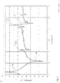
- FIG. 7 is a graph of the performance of two XBAR with thick dielectric tuning layers.
- FIG. 7 and subsequent figures are based on simulations of XBARs using a finite element method. Specifically, the solid curve 710 is a plot of the magnitude of admittance of a first XBAR as a function of frequency.
- the first XBAR has a lithium niobate piezoelectric plate 500 nm thick and a top-side SiO 2 tuning layer 180 nm thick, or 35% of the thickness of the piezoelectric plate.
- the IDT fingers are 560 nm of aluminum over 50 nm of titanium.
- the sidewall angle of the IDT fingers is 77 degrees.
- the IDT pitch is 5.5 ⁇ m and the mark or finger width is 1.2 ⁇ m.
- the resonance and anti-resonance frequencies of the first XBAR are 3.11 and 3.5 GHz, respectively.
- An A1-3 spurious mode 715 occurs at about 4.1 GHz and an A2 spurious mode 712 occurs at 5.17 GHz.
- A1-3 and “A2” refer to Lamb plate wave modes. The strong excitation of the A2 mode is due in part to the asymmetric structure of the XBAR.
- the dashed curve 720 is a plot of the magnitude of admittance of a second XBAR as a function of frequency.
- the first XBAR has a lithium niobate piezoelectric plate 530 nm thick and a top-side SiO 2 tuning layer 150 nm thick, or 28% of the thickness of the piezoelectric plate.
- the IDT fingers are 560 nm of aluminum over 50 nm of titanium.
- the sidewall angle of the IDT fingers is 77 degrees.
- the IDT pitch is 5.5 ⁇ m and the mark or finger width is 1.2 ⁇ m.
- the resonance frequencies of the first and second XBARs are the same.
- the anti-resonance frequency of the second XBAR (dashed curve 720 ) is higher than that of the first XBAR (solid curve 710 ), indicating slightly higher electromechanical coupling.
- a major different between the two curves is the substantial reduction in the A2 mode 722 of the second XBAR compared to the A2 mode 712 of the first XBAR.
- the A2 mode is negligible when the thickness of the dielectric tuning layer is less than or equal to 0.25 times the thickness of the piezoelectric plate.
- the A2 mode may not be a problem when the thickness of the dielectric tuning layer is as large as 0.28 times the thickness of the piezoelectric plate.
- FIG. 8 is a schematic cross-sectional view through a shunt resonator and a series resonator of a filter 800 that uses a divided dielectric frequency setting layer to separate the resonance frequencies of shunt and series resonators.
- a “divided frequency setting layer” divides the frequency setting function between a top-side dielectric layer and a back-side dielectric layer.
- a piezoelectric plate 810 is attached to a substrate 820 . Portions of the piezoelectric plate 810 form diaphragms spanning cavities 840 in the substrate 820 . Interleaved IDT fingers, such as finger 830 , are formed on the diaphragms.
- a top-side dielectric frequency setting layer 850 is formed over the IDT of the shunt resonator.
- a bottom-side dielectric frequency setting layer 860 is formed on the back side of the diaphragm of the shunt resonator.
- the top-side frequency setting layer 850 and the bottom-side frequency setting layer 860 are collective considered a “divided frequency setting layer”.
- the top-side frequency setting layer 850 and the bottom-side frequency setting layer 860 collectively determine the frequency difference between the shunt resonator and the series resonator of the filter 800 .
- the top-side and bottom-side frequency setting layers are commonly SiO 2 but be any of the previously identified dielectric materials.
- the top-side and bottom-side frequency setting layers may be different materials and either or both may be a laminate or composite of two or more dielectric materials.
- a passivation and tuning layer 855 may be deposited over both the shunt and series resonator as previously described.
- a second front-side frequency setting layer may be formed over some, but not all, of the shunt resonators and/or some, but not all, of the series resonators.
- the thickness of a second front-side frequency setting layer will typically be thinner than the thickness of the first front-side frequency setting layer.
- the second front-side frequency setting layer may be any of the previously identified dielectric materials.
- the resonance frequency of an XBAR is roughly proportional to the inverse of the total thickness of the diaphragm including the piezoelectric plate 810 and the dielectric layers 850 , 855 , 860 .
- the diaphragm of the shunt resonator is thicker than the diaphragm of the series resonator by the total thickness of the top-side and bottom-side frequency setting layers 850 , 860 .
- the shunt resonator will have a lower resonance frequency than the series resonator.
- FIG. 9 is a graph 900 of the performance of an XBAR with a divided dielectric tuning layer.
- the curve 910 is a plot of the magnitude of admittance of the XBAR as a function of frequency.
- the XBAR has the same construction as the described in conjunction FIG. 7 except for a divided frequency setting layer with 20% of the total thickness of the frequency setting layer on the back side of the diaphragm.
- the dashed curve 920 is a plot of the magnitude of admittance of the XBAR with a thick dielectric frequency setting layer, as previously shown in FIG. 7 .
- the dashed curve 920 is provided for comparison.
- the resonance and anti-resonance frequencies of the XBAR with the divided frequency setting layer are 3.11 and 3.625 GHz, respectively.
- An A1-3 spurious mode 915 occurs at about 4.1 GHz and an A2 spurious mode 912 occurs at 5.235 GHz.
- the peak magnitude of the admittance of the A2 mode is reduced by 11 dB.
- the difference between the anti-resonance and resonance frequencies of the XBAR with the divided frequency setting layer (solid line 910 ) is increased compared to the original XBAR (dashed line 920 ), indicating higher electromechanical coupling to the primary shear acoustic mode.
- FIG. 10 is a graph 1000 of the performance of another XBAR with a divided dielectric tuning layer.
- the curve 1010 is a plot of the magnitude of admittance of the XBAR as a function of frequency.
- the XBAR has the same construction as the described in conjunction FIG. 7 except for a divided frequency setting layer with 35% of the total thickness of the frequency setting layer on the back side of the diaphragm.
- the dashed curve 1020 is a plot of the magnitude of admittance of the XBAR with a thick dielectric frequency setting layer, as previously shown in FIG. 7 .
- the dashed curve 1020 is provided for comparison.
- the resonance and anti-resonance frequencies of the XBAR with the divided frequency setting layer are 3.11 and 3.65 GHz, respectively.
- An A1-3 spurious mode 1015 occurs at about 4.1 GHz and an A2 spurious mode 1012 occurs at 5.255 GHz.
- the peak magnitude of the admittance of the A2 mode is reduced by 24 dB.
- the difference between the anti-resonance and resonance frequencies of the XBAR with the divided frequency setting layer (solid line 1010 ) is increased compared to the original XBAR (dashed line 1020 ), indicating higher electromechanical coupling to the primary shear acoustic mode.
- FIG. 11 is a graph 1100 of the performance of another XBAR with a divided dielectric tuning layer.
- the curve 1110 is a plot of the magnitude of admittance of the XBAR as a function of frequency.
- the XBAR has the same construction as the described in conjunction FIG. 7 except for a divided frequency setting layer with 47% of the total thickness of the frequency setting layer on the back side of the diaphragm.
- the dashed curve 1120 is a plot of the magnitude of admittance of the XBAR with a thick dielectric frequency setting layer, as previously shown in FIG. 7 .
- the dashed curve 1120 is provided for comparison.
- the resonance and anti-resonance frequencies of the XBAR with the divided frequency setting layer are 3.11 and 3.65 GHz, respectively.
- An A1-3 spurious mode 1115 occurs at about 4.1 GHz.
- the peak magnitude of the admittance of the A2 mode is reduced by 28 dB.
- the difference between the anti-resonance and resonance frequencies of the XBAR with the divided frequency setting layer (solid line 1110 ) is increased compared to the original XBAR (dashed line 1120 ), indicating higher electromechanical coupling to the primary shear acoustic mode.
- FIG. 12 is a graph 1200 of the effects of back-side frequency setting layer thickness on XBAR performance.
- the front-side and back-side frequency setting layers are SiO 2 .
- the solid curve 1210 is a plot of Gamma, a measure of electro-mechanical coupling of the shear primary acoustic mode, as a function of the thickness of the back-side frequency setting layer expressed as a percentage of the total frequency setting layer thickness.
- Gamma is lowest (i.e. highest coupling) when 35% to 50% of the total frequency setting layer thickness is on the back side of the diaphragm.
- the dashed curve 1220 is a plot of peak admittance of the A2 spurious mode as a function of the thickness of the back-side frequency setting layer expressed as a percentage of the total frequency setting layer thickness.
- the peak admittance is expressed relative to the peak admittance of the A2 mode with a front-side frequency setting layer as shown in FIG. 7 .
- the peak A2 mode admittance is reduced by at least 20 dB when the thickness of the back-side frequency setting layer is at least 30% of the total frequency setting layer thickness.
- both the front-side and back-side frequency setting layers were SiO 2 .
- a different dielectric material is used for both the front-side and back-side frequency setting layers, similar results can be expected.
- Gamma will decrease as the diaphragm structure becomes symmetrical and the A2 mode will be reduced by 20 dB or more when the thickness of the back-side frequency setting layer is at least 30% of the total frequency setting layer thickness.
- the thicknesses of the back-side frequency setting layer and the front-side frequency setting layer are configured so that a peak admittance of an A2 mode is substantially reduced compared to a peak admittance of an A2 spurious mode of a resonator with only a front-side frequency setting layer.
- substantially reduced means “reduced to a level where the A2 mode does not adversely affect filter performance.”
- FIG. 13 is a simplified flow chart showing a process 1300 for making a filter incorporating XBARs.
- the process 1300 starts at 1305 with a substrate and a plate of piezoelectric material and ends at 1395 with a completed filter.
- the flow chart of FIG. 13 includes only major process steps.
- Various conventional process steps e.g. surface preparation, cleaning, inspection, baking, annealing, monitoring, testing, etc. may be performed before, between, after, and during the steps shown in FIG. 13 .
- the flow chart of FIG. 13 captures three variations of the process 1300 for making an XBAR which differ in when and how cavities are formed in the substrate.
- the cavities may be formed at steps 1310 A, 1310 B, or 1310 C. Only one of these steps is performed in each of the three variations of the process 1300 .
- the piezoelectric plate may be lithium niobate or lithium tantalate.
- the piezoelectric plate may be Z-cut, rotated Z-cut, or rotated YX-cut, or some other cut.
- the substrate may preferably be silicon.
- the substrate may be some other material that allows formation of deep cavities by etching or other processing.
- one or more cavities are formed in the substrate at 1310 A, before the piezoelectric plate is bonded to the substrate at 1320 .
- a separate cavity may be formed for each resonator in a filter device.
- the one or more cavities may be formed using conventional photolithographic and etching techniques. Typically, the cavities formed at 1310 A will not penetrate through the substrate, and the resulting resonator devices will have a cross-section as shown in FIG. 3 .
- a back side dielectric frequency setting layer is formed.
- the back-side frequency setting layer may be any of the dielectric material previously described.
- the back-side frequency setting layer may be formed by depositing the dielectric material on a surface of the substrate (e.g., the surface where the cavities were formed if action 1310 A was performed) or a back surface of the piezoelectric plate or both.
- the piezoelectric plate is bonded to the substrate.
- the piezoelectric plate and the substrate may be bonded by a wafer bonding process.
- the mating surfaces of the substrate and the piezoelectric plate are highly polished.
- One or both of the mating surface will be covered by the dielectric back-side frequency setting layer formed at 1315 .
- One or more additional layers of intermediate materials, such as an oxide or metal, may be formed or deposited on the mating surface of one or both of the piezoelectric plate and the substrate.
- One or both mating surfaces may be activated using, for example, a plasma process. The mating surfaces may then be pressed together with considerable force to establish molecular bonds between the piezoelectric plate and the substrate or intermediate material layers.
- a conductor pattern, including IDTs of each XBAR, is formed at 1330 by depositing and patterning one or more conductor layer on the front side of the piezoelectric plate.
- the conductor layer may be, for example, aluminum, an aluminum alloy, copper, a copper alloy, or some other conductive metal.
- one or more layers of other materials may be disposed below (i.e. between the conductor layer and the piezoelectric plate) and/or on top of the conductor layer.
- a thin film of titanium, chrome, or other metal may be used to improve the adhesion between the conductor layer and the piezoelectric plate.
- a conduction enhancement layer of gold, aluminum, copper or other higher conductivity metal may be formed over portions of the conductor pattern (for example the IDT bus bars and interconnections between the IDTs).
- the conductor pattern may be formed at 1330 by depositing the conductor layer and, optionally, one or more other metal layers in sequence over the surface of the piezoelectric plate. The excess metal may then be removed by etching through patterned photoresist.
- the conductor layer can be etched, for example, by plasma etching, reactive ion etching, wet chemical etching, and other etching techniques.
- the conductor pattern may be formed at 1330 using a lift-off process.
- Photoresist may be deposited over the piezoelectric plate. and patterned to define the conductor pattern.
- the conductor layer and, optionally, one or more other layers may be deposited in sequence over the surface of the piezoelectric plate. The photoresist may then be removed, which removes the excess material, leaving the conductor pattern.
- a front-side dielectric layer or frequency setting dielectric layer may be formed by depositing one or more layers of dielectric material on the front side of the piezoelectric plate.
- the one or more dielectric layers may be deposited using a conventional deposition technique such as sputtering, evaporation, or chemical vapor deposition.
- the one or more dielectric layers may be deposited over the entire surface of the piezoelectric plate, including on top of the conductor pattern.
- one or more lithography processes (using photomasks) may be used to limit the deposition of the dielectric layers to selected areas of the piezoelectric plate, such as only between the interleaved fingers of the IDTs.
- Masks may also be used to allow deposition of different thicknesses of dielectric materials on different portions of the piezoelectric plate.
- one or more cavities are formed in the back side of the substrate at 1310 B.
- a separate cavity may be formed for each resonator in a filter device.
- the one or more cavities may be formed using an anisotropic or orientation-dependent dry or wet etch to open holes through the back-side of the substrate to the piezoelectric plate.
- the resulting resonator devices will have a cross-section as shown in FIG. 1 .
- one or more cavities in the form of recesses in the substrate may be formed at 1310 C by etching the substrate using an etchant introduced through openings in the piezoelectric plate.
- a separate cavity may be formed for each resonator in a filter device.
- the one or more cavities formed at 1310 C will not penetrate through the substrate, and the resulting resonator devices will have a cross-section as shown in FIG. 3 .
- the back-side dielectric layer is removed from the series resonators at 1350 .
- the back-side dielectric layer may also be removed from the series resonators by etching from the back side of the substrate.
- the back-side dielectric layer may be removed from the series resonators by an etchant introduced through the same openings used to etch the cavities.
- the back-side dielectric layer may be removed from the series resonators by an etchant introduced through the openings in the piezoelectric plate created specifically for this purpose.
- the filter device is then completed at 1360 .
- Actions that may occur at 1360 include depositing an encapsulation/passivation layer such as SiO 2 or Si 3 O 4 over all or a portion of the device; forming bonding pads or solder bumps or other means for making connection between the device and external circuitry; excising individual devices from a wafer containing multiple devices; other packaging steps; and testing.
- Another action that may occur at 1360 is to tune the resonant frequencies of the resonators within the device by adding or removing metal or dielectric material from the front side of the device.
Abstract
Description
Claims (20)
Priority Applications (3)
| Application Number | Priority Date | Filing Date | Title |
|---|---|---|---|
| US17/081,717 US11374549B2 (en) | 2018-06-15 | 2020-10-27 | Filter using transversely-excited film bulk acoustic resonators with divided frequency-setting dielectric layers |
| US17/083,076 US11736086B2 (en) | 2018-06-15 | 2020-10-28 | Filter using transversely-excited film bulk acoustic resonators with divided frequency-setting dielectric layers |
| US17/743,328 US20220278666A1 (en) | 2018-06-15 | 2022-05-12 | Filter using transversely-excited film bulk acoustic resonators with divided frequency-setting dielectric layers |
Applications Claiming Priority (10)
| Application Number | Priority Date | Filing Date | Title |
|---|---|---|---|
| US201862685825P | 2018-06-15 | 2018-06-15 | |
| US201862701363P | 2018-07-20 | 2018-07-20 | |
| US201862741702P | 2018-10-05 | 2018-10-05 | |
| US201862748883P | 2018-10-22 | 2018-10-22 | |
| US201862753815P | 2018-10-31 | 2018-10-31 | |
| US16/230,443 US10491192B1 (en) | 2018-06-15 | 2018-12-21 | Transversely-excited film bulk acoustic resonator |
| US16/438,121 US10756697B2 (en) | 2018-06-15 | 2019-06-11 | Transversely-excited film bulk acoustic resonator |
| US16/920,173 US11139794B2 (en) | 2018-06-15 | 2020-07-02 | Transversely-excited film bulk acoustic resonator |
| US202063067329P | 2020-08-19 | 2020-08-19 | |
| US17/081,717 US11374549B2 (en) | 2018-06-15 | 2020-10-27 | Filter using transversely-excited film bulk acoustic resonators with divided frequency-setting dielectric layers |
Related Parent Applications (1)
| Application Number | Title | Priority Date | Filing Date |
|---|---|---|---|
| US16/920,173 Continuation-In-Part US11139794B2 (en) | 2018-02-18 | 2020-07-02 | Transversely-excited film bulk acoustic resonator |
Related Child Applications (2)
| Application Number | Title | Priority Date | Filing Date |
|---|---|---|---|
| US17/083,076 Continuation US11736086B2 (en) | 2018-06-15 | 2020-10-28 | Filter using transversely-excited film bulk acoustic resonators with divided frequency-setting dielectric layers |
| US17/743,328 Continuation US20220278666A1 (en) | 2018-06-15 | 2022-05-12 | Filter using transversely-excited film bulk acoustic resonators with divided frequency-setting dielectric layers |
Publications (2)
| Publication Number | Publication Date |
|---|---|
| US20210044272A1 US20210044272A1 (en) | 2021-02-11 |
| US11374549B2 true US11374549B2 (en) | 2022-06-28 |
Family
ID=74498735
Family Applications (2)
| Application Number | Title | Priority Date | Filing Date |
|---|---|---|---|
| US17/081,717 Active 2039-05-05 US11374549B2 (en) | 2018-06-15 | 2020-10-27 | Filter using transversely-excited film bulk acoustic resonators with divided frequency-setting dielectric layers |
| US17/083,076 Active 2039-05-23 US11736086B2 (en) | 2018-06-15 | 2020-10-28 | Filter using transversely-excited film bulk acoustic resonators with divided frequency-setting dielectric layers |
Family Applications After (1)
| Application Number | Title | Priority Date | Filing Date |
|---|---|---|---|
| US17/083,076 Active 2039-05-23 US11736086B2 (en) | 2018-06-15 | 2020-10-28 | Filter using transversely-excited film bulk acoustic resonators with divided frequency-setting dielectric layers |
Country Status (1)
| Country | Link |
|---|---|
| US (2) | US11374549B2 (en) |
Cited By (3)
| Publication number | Priority date | Publication date | Assignee | Title |
|---|---|---|---|---|
| US20220278666A1 (en) * | 2018-06-15 | 2022-09-01 | Resonant Inc. | Filter using transversely-excited film bulk acoustic resonators with divided frequency-setting dielectric layers |
| US11901877B2 (en) | 2020-10-05 | 2024-02-13 | Murata Manufacturing Co., Ltd. | Transversely-excited film bulk acoustic resonator matrix filters with noncontiguous passband |
| US11955951B2 (en) | 2020-10-05 | 2024-04-09 | Murata Manufacturing Co., Ltd. | Transversely-excited film bulk acoustic resonator matrix filters with switches in parallel with sub-filter shunt capacitors |
Families Citing this family (2)
| Publication number | Priority date | Publication date | Assignee | Title |
|---|---|---|---|---|
| KR20220079629A (en) * | 2019-11-08 | 2022-06-13 | 텔레폰악티에볼라겟엘엠에릭슨(펍) | Determine the phase tracking reference signal at multiple transmission points |
| WO2023159091A1 (en) * | 2022-02-16 | 2023-08-24 | Murata Manufacturing Co., Ltd. | Tuning acoustic resonators with back-side coating |
Citations (104)
| Publication number | Priority date | Publication date | Assignee | Title |
|---|---|---|---|---|
| US5446330A (en) | 1993-03-15 | 1995-08-29 | Matsushita Electric Industrial Co., Ltd. | Surface acoustic wave device having a lamination structure |
| US5552655A (en) | 1994-05-04 | 1996-09-03 | Trw Inc. | Low frequency mechanical resonator |
| US5726610A (en) | 1995-06-19 | 1998-03-10 | Motorola Inc. | Saw filter device for radio tranceiver utilizing different coupling coefficient ratios |
| US5853601A (en) | 1997-04-03 | 1998-12-29 | Northrop Grumman Corporation | Top-via etch technique for forming dielectric membranes |
| US6377140B1 (en) | 1999-07-09 | 2002-04-23 | Oki Electric Industry Co., Ltd. | Saw resonator filter with bridged-T configuration |
| US20020079986A1 (en) | 2000-12-21 | 2002-06-27 | Ruby Richard C. | Bulk acoustic resonator perimeter reflection system |
| US20020158714A1 (en) | 2001-04-27 | 2002-10-31 | Nokia Corporation | Method and system for wafer-level tuning of bulk acoustic wave resonators and filters by reducing thickness non-uniformity |
| US20020189062A1 (en) | 2001-06-15 | 2002-12-19 | Asia Pacific Microsystems, Inc. | Manufacturing method for a high quality film bulk acoustic wave device |
| US6516503B1 (en) | 1999-05-26 | 2003-02-11 | Murata Manufacturing Co., Ltd. | Method of making surface acoustic wave device |
| US6540827B1 (en) | 1998-02-17 | 2003-04-01 | Trustees Of Columbia University In The City Of New York | Slicing of single-crystal films using ion implantation |
| US20030080831A1 (en) | 2001-10-25 | 2003-05-01 | Naumenko Natalya F. | Surface acoustic wave devices using optimized cuts of lithium niobate (LiNbO3) |
| US20030199105A1 (en) | 2002-04-22 | 2003-10-23 | Kub Francis J. | Method for making piezoelectric resonator and surface acoustic wave device using hydrogen implant layer splitting |
| US6707229B1 (en) | 1999-06-03 | 2004-03-16 | Tele Filter Zweigniederlassung Der Dover Germany Gmbh | Surface acoustic wave filter |
| US20040100164A1 (en) | 2002-11-26 | 2004-05-27 | Murata Manufacturing Co., Ltd. | Manufacturing method of electronic device |
| US20040261250A1 (en) | 2000-09-06 | 2004-12-30 | Murata Manufacturing Co., Ltd. | Method for adjusting a frequency characteristic of an edge reflection type surface acoustic wave device and method for producing an- edge reflection type surface acoustic wave device |
| US20050185026A1 (en) | 2004-01-26 | 2005-08-25 | Motohisa Noguchi | Piezoelectric element, piezoelectric actuator, ink jet recording head, ink jet printer, surface acoustic wave element, frequency filter, oscillator, electronic circuit, thin film piezoelectric resonator, and electronic apparatus |
| US20050218488A1 (en) | 2004-03-31 | 2005-10-06 | Mie Matsuo | Electronic component having micro-electrical mechanical system |
| US20050264136A1 (en) | 2004-05-31 | 2005-12-01 | Jun Tsutsumi | Surface acoustic wave device |
| US20060179642A1 (en) | 2005-02-03 | 2006-08-17 | Kabushiki Kaisha Toshiba | Method for manufacturing a film bulk acoustic resonator |
| US20070182510A1 (en) | 2006-02-06 | 2007-08-09 | Samsung Electronics Co., Ltd. | Multi-band filter module and method of fabricating the same |
| US20070188047A1 (en) | 2006-02-16 | 2007-08-16 | Seiko Epson Corporation | Lamb wave type frequency device and method thereof |
| US20070194863A1 (en) | 2006-02-17 | 2007-08-23 | Kabushiki Kaisha Toshiba | Film bulk acoustic resonator and method of manufacturing same |
| US20070267942A1 (en) | 2006-05-19 | 2007-11-22 | Hisanori Matsumoto | Piezoelectric film resonator, radio-frequency filter using them, and radio-frequency module using them |
| US7345400B2 (en) | 2003-01-27 | 2008-03-18 | Murata Manufacturing Co., Ltd. | Surface acoustic wave device |
| US20080246559A1 (en) | 2007-01-19 | 2008-10-09 | Farrokh Ayazi | Lithographically-defined multi-standard multi-frequency high-Q tunable micromechanical resonators |
| US7463118B2 (en) | 2006-06-09 | 2008-12-09 | Texas Instruments Incorporated | Piezoelectric resonator with an efficient all-dielectric Bragg reflector |
| US7535152B2 (en) | 2005-10-19 | 2009-05-19 | Murata Manufacturing Co., Ltd. | Lamb wave device |
| US7684109B2 (en) | 2007-02-28 | 2010-03-23 | Maxim Integrated Products, Inc. | Bragg mirror optimized for shear waves |
| US20100123367A1 (en) | 2008-11-19 | 2010-05-20 | Ngk Insulators, Ltd. | Lamb wave device |
| US7868519B2 (en) | 2007-09-06 | 2011-01-11 | Murata Manufacturing Co., Ltd. | Piezoelectric resonator including an acoustic reflector portion |
| US20110018654A1 (en) | 2009-07-27 | 2011-01-27 | Avago Technologies Wireless Ip (Singapore) Pte. Ltd. | Resonator filter with multiple cross-couplings |
| US20110018389A1 (en) | 2008-01-30 | 2011-01-27 | Kyocera Corporation | Acoustic Wave Device and Method for Production of Same |
| US7941103B2 (en) | 2005-11-15 | 2011-05-10 | Taiyo Yuden Co., Ltd. | Duplexer |
| US20110109196A1 (en) | 2008-07-11 | 2011-05-12 | Goto Rei | Plate wave element and electronic equipment using same |
| US20110278993A1 (en) | 2010-05-17 | 2011-11-17 | Murata Manufacturing Co., Ltd. | Method for manufacturing composite piezoelectric substrate and piezoelectric device |
| US8278802B1 (en) | 2008-04-24 | 2012-10-02 | Rf Micro Devices, Inc. | Planarized sacrificial layer for MEMS fabrication |
| US8294330B1 (en) | 2009-03-31 | 2012-10-23 | Triquint Semiconductor, Inc. | High coupling, low loss saw filter and associated method |
| US20120286900A1 (en) | 2010-01-28 | 2012-11-15 | Murata Manufacturing Co., Ltd. | Tunable filter |
| US8344815B2 (en) | 2008-10-24 | 2013-01-01 | Seiko Epson Corporation | Surface acoustic wave resonator, surface acoustic wave oscillator, and surface acoustic wave module unit |
| US20130234805A1 (en) | 2012-03-07 | 2013-09-12 | Taiyo Yuden Co., Ltd. | Resonator, frequency filter, duplexer, electronic device, and method of manufacturing resonator |
| US20130271238A1 (en) | 2012-04-13 | 2013-10-17 | Taiyo Yuden Co., Ltd. | Filter device, manufacturing method for filter device, and duplexer |
| US20130278609A1 (en) | 2012-04-19 | 2013-10-24 | Qualcomm Mems Technologies, Inc. | Isotropically-etched cavities for evanescent-mode electromagnetic-wave cavity resonators |
| US20130321100A1 (en) | 2012-06-05 | 2013-12-05 | Avago Technologies Wireless Ip (Singapore) Pte. Ltd. | Laterally-coupled acoustic resonators |
| US20140130319A1 (en) | 2010-09-28 | 2014-05-15 | Murata Manufacturing Co., Ltd. | Method for manufacturing piezoelectric device |
| US20140145556A1 (en) | 2011-08-08 | 2014-05-29 | Murata Manufacturing Co., Ltd. | Elastic wave device |
| US20140151151A1 (en) | 2010-10-15 | 2014-06-05 | Commissariat A L'energie Atomique Et Aux Energies Alternatives | Heterogenous acoustic structure formed from a homogeneous material |
| US20140152145A1 (en) | 2010-11-30 | 2014-06-05 | Murata Manufacturing Co., Ltd. | Elastic wave device and manufacturing method for same |
| US20140173862A1 (en) | 2007-12-25 | 2014-06-26 | Murata Manufacturing Co., Ltd. | Method for manufacturing composite piezoelectric substrate |
| US20140225684A1 (en) | 2011-10-24 | 2014-08-14 | Murata Manufacturing Co., Ltd. | Surface acoustic wave device |
| US8816567B2 (en) | 2011-07-19 | 2014-08-26 | Qualcomm Mems Technologies, Inc. | Piezoelectric laterally vibrating resonator structure geometries for spurious frequency suppression |
| US8829766B2 (en) | 2008-08-01 | 2014-09-09 | Epcos Ag | Piezoelectric resonator operating in thickness shear mode |
| US8932686B2 (en) | 2008-10-31 | 2015-01-13 | Murata Manufacturing Co., Ltd. | Method for producing piezoelectric composite substrate |
| US20150042417A1 (en) | 2013-08-06 | 2015-02-12 | Murata Manufacturing Co., Ltd. | High-frequency module |
| US9130145B2 (en) | 2012-03-29 | 2015-09-08 | Vectron International Gmbh | Surface acoustic wave component |
| US20150319537A1 (en) | 2012-12-12 | 2015-11-05 | Epcos Ag | Electroacoustic Components and Methods Thereof |
| US20150333730A1 (en) | 2010-04-23 | 2015-11-19 | Teknologian Tutkimuskeskus Vtt Oy | Wide-band acoustically coupled thin-film BAW filter |
| US9219466B2 (en) | 2011-11-11 | 2015-12-22 | Teknologian Tutkimuskeskus Vtt Oy | Laterally coupled bulk acoustic wave filter with improved passband characteristics |
| US20160028367A1 (en) | 2014-07-25 | 2016-01-28 | Akoustis, Inc. | Single crystal acoustic resonator and bulk acoustic wave filter |
| WO2016017104A1 (en) | 2014-07-31 | 2016-02-04 | Skyworks Panasonic Filter Solutions Japan Co., Ltd. | Acoustic wave filters and duplexers using same |
| US9276557B1 (en) | 2013-07-01 | 2016-03-01 | Sandia Corporation | Programmable electroacoustic filter apparatus and method for its manufacture |
| US9369105B1 (en) | 2007-08-31 | 2016-06-14 | Rf Micro Devices, Inc. | Method for manufacturing a vibrating MEMS circuit |
| US20160182009A1 (en) | 2014-12-17 | 2016-06-23 | Rf Micro Devices, Inc. | Plate wave devices with wave confinement structures and fabrication methods |
| US9425765B2 (en) | 2013-04-22 | 2016-08-23 | Northeastern University | Nano- and micro-electromechanical resonators |
| US9525398B1 (en) | 2014-05-27 | 2016-12-20 | Sandia Corporation | Single crystal micromechanical resonator and fabrication methods thereof |
| US20170063332A1 (en) | 2015-08-25 | 2017-03-02 | Avago Technologies General Ip (Singapore) Pte. Ltd. | Surface acoustic wave (saw) resonator having trap-rich region |
| US9640750B2 (en) | 2011-03-25 | 2017-05-02 | Skyworks Filter Solutions Japan Co., Ltd. | Acoustic wave device with suppressed higher order transverse modes |
| US20170179928A1 (en) | 2015-11-13 | 2017-06-22 | Resonant Inc. | Acoustic wave filter with enhanced rejection |
| US20170214387A1 (en) | 2016-01-26 | 2017-07-27 | Avago Technologies General Ip (Singapore) Pte. Ltd. | Bulk acoustic wave resonator with piezoelectric layer comprising lithium niobate or lithium tantalate |
| US20170214381A1 (en) | 2016-01-22 | 2017-07-27 | Rf Micro Devices, Inc. | Guided wave devices with selectively thinned piezoelectric layers |
| US20170222622A1 (en) | 2016-01-28 | 2017-08-03 | Triquint Semiconductor, Inc. | Surface acoustic wave device having a piezoelectric layer on a quartz substrate and methods of manufacturing thereof |
| US20170222617A1 (en) | 2014-10-16 | 2017-08-03 | Murata Manufacturing Co., Ltd. | High-frequency module |
| US9762202B2 (en) | 2008-12-17 | 2017-09-12 | Analog Devices, Inc. | Method of manufacturing a mechanical resonating structure |
| US9780759B2 (en) | 2010-12-24 | 2017-10-03 | Murata Manufacturing Co., Ltd. | Elastic wave device and method for manufacturing the same |
| US9837984B2 (en) | 2014-12-24 | 2017-12-05 | Qorvo Us, Inc. | RF ladder filter with simplified acoustic RF resonator parallel capacitance compensation |
| US20170370791A1 (en) | 2016-06-28 | 2017-12-28 | Taiyo Yuden Co., Ltd. | Method of fabricating acoustic wave device and acoustic wave device |
| WO2018003273A1 (en) | 2016-06-28 | 2018-01-04 | 株式会社村田製作所 | Multiplexer, high-frequency front end circuit, and communication device |
| US20180005950A1 (en) | 2016-06-29 | 2018-01-04 | Murata Manufacturing Co., Ltd. | Electronic component device, method of mounting electronic component device on circuit board, and mounting structure of electronic component device on circuit board |
| US20180026603A1 (en) | 2015-05-22 | 2018-01-25 | Murata Manufacturing Co., Ltd. | Electronic component |
| US20180033952A1 (en) | 2016-07-28 | 2018-02-01 | Taiyo Yuden Co., Ltd. | Electronic device and method of fabricating the same |
| US20180062615A1 (en) | 2015-05-08 | 2018-03-01 | Murata Manufacturing Co., Ltd. | High frequency module |
| US20180062617A1 (en) | 2016-08-25 | 2018-03-01 | Qualcomm Incorporated | Single-chip multi-frequency film bulk acoustic-wave resonators |
| US20180123016A1 (en) | 2012-06-15 | 2018-05-03 | Carnegie Mellon University | Microelectronic structures with suspended lithium-based thin films |
| US20180191322A1 (en) | 2017-01-03 | 2018-07-05 | Win Semiconductors Corp. | Method for fabricating bulk acoustic wave resonator with mass adjustment structure |
| US20180262179A1 (en) * | 2017-01-24 | 2018-09-13 | Skyworks Solutions, Inc. | Acoustic wave device with acoustically separated multi-channel feedback |
| US10079414B2 (en) | 2015-03-17 | 2018-09-18 | The United States Of America, As Represented By The Secretary Of The Navy | Switched multiplexer with flat group delay and channelized limiting |
| US10187039B2 (en) | 2016-06-07 | 2019-01-22 | Skyworks Filter Solutions Japan Co., Ltd. | Filter devices having reduced spurious emissions from lamb waves |
| US10200013B2 (en) | 2016-02-18 | 2019-02-05 | X-Celeprint Limited | Micro-transfer-printed acoustic wave filter device |
| US20190068164A1 (en) | 2016-03-11 | 2019-02-28 | Akoustis, Inc. | 5G BAND n79 ACOUSTIC WAVE RESONATOR RF FILTER CIRCUIT |
| US20190131953A1 (en) | 2017-10-31 | 2019-05-02 | The Board Of Trustees Of The University Of Illinois | Interdigital transducers on a piezoelectric thin-film for signal compression |
| US10284176B1 (en) | 2015-06-03 | 2019-05-07 | Qorvo Us, Inc. | Temperature compensated surface acoustic wave device and methods of manufacturing the same |
| US20190253038A1 (en) * | 2016-03-11 | 2019-08-15 | Akoustis, Inc. | 5G n79 WI-FI ACOUSTIC TRIPLEXER CIRCUIT |
| US20190273480A1 (en) | 2018-03-02 | 2019-09-05 | Skyworks Solutions, Inc. | Lamb wave loop circuit for acoustic wave filter |
| US20190348966A1 (en) | 2018-05-10 | 2019-11-14 | Globalfoundries Singapore Pte. Ltd. | Acoustic wave filter formed on a v-groove topography and method for producing the same |
| US10491192B1 (en) | 2018-06-15 | 2019-11-26 | Resonant Inc. | Transversely-excited film bulk acoustic resonator |
| US20200036357A1 (en) | 2017-04-26 | 2020-01-30 | Murata Manufacturing Co., Ltd. | Acoustic wave device |
| US20200083861A1 (en) * | 2018-09-12 | 2020-03-12 | Skyworks Global Pte. Ltd. | Recess frame structure for a bulk acoustic wave resonator |
| US10601392B2 (en) | 2018-06-15 | 2020-03-24 | Resonant Inc. | Solidly-mounted transversely-excited film bulk acoustic resonator |
| US10637438B2 (en) | 2018-06-15 | 2020-04-28 | Resonant Inc. | Transversely-excited film bulk acoustic resonators for high power applications |
| US20200235719A1 (en) | 2018-06-15 | 2020-07-23 | Resonant Inc. | Xbar resonators with non-rectangular diaphragms |
| US10756697B2 (en) | 2018-06-15 | 2020-08-25 | Resonant Inc. | Transversely-excited film bulk acoustic resonator |
| US10790802B2 (en) | 2018-06-15 | 2020-09-29 | Resonant Inc. | Transversely excited film bulk acoustic resonator using rotated Y-X cut lithium niobate |
| US10797675B2 (en) | 2018-06-15 | 2020-10-06 | Resonant Inc. | Transversely excited film bulk acoustic resonator using rotated z-cut lithium niobate |
| US10826462B2 (en) | 2018-06-15 | 2020-11-03 | Resonant Inc. | Transversely-excited film bulk acoustic resonators with molybdenum conductors |
| US20210152154A1 (en) * | 2019-11-19 | 2021-05-20 | Skyworks Solutions, Inc. | Surface acoustic wave device |
Family Cites Families (30)
| Publication number | Priority date | Publication date | Assignee | Title |
|---|---|---|---|---|
| DE10111959B4 (en) | 2001-03-13 | 2014-11-20 | Epcos Ag | With acoustic waves working transducer structure |
| JP3892370B2 (en) | 2002-09-04 | 2007-03-14 | 富士通メディアデバイス株式会社 | Surface acoustic wave element, filter device, and manufacturing method thereof |
| JP4289399B2 (en) * | 2006-06-22 | 2009-07-01 | セイコーエプソン株式会社 | Acoustic wave device and method of manufacturing acoustic wave device |
| US7939987B1 (en) | 2008-10-23 | 2011-05-10 | Triquint Semiconductor, Inc. | Acoustic wave device employing reflective elements for confining elastic energy |
| US8291559B2 (en) | 2009-02-24 | 2012-10-23 | Epcos Ag | Process for adapting resonance frequency of a BAW resonator |
| FI20106063A (en) | 2010-10-14 | 2012-06-08 | Valtion Teknillinen | Acoustically coupled wide-band thin film BAW filter |
| CN103119847B (en) * | 2010-12-28 | 2016-01-20 | 京瓷株式会社 | Elastic wave device and use the acoustic wave device of this elastic wave device |
| JP5877043B2 (en) | 2011-11-22 | 2016-03-02 | 太陽誘電株式会社 | Duplexer |
| US20150244149A1 (en) | 2012-05-30 | 2015-08-27 | Euphoenix B.V. | Tunable Semiconductor Device And Method For Making Tunable Semiconductor Device |
| US20160079958A1 (en) | 2014-05-30 | 2016-03-17 | Avago Technologies General Ip (Singapore) Pte. Ltd. | Acoustic resonator comprising vertically extended acoustic cavity |
| KR102058029B1 (en) | 2014-09-30 | 2019-12-20 | 가부시키가이샤 무라타 세이사쿠쇼 | Ladder type filter and method for manufacturing same |
| US10581650B2 (en) | 2015-09-08 | 2020-03-03 | Qorvo Us, Inc. | Enhancing isolation in radio frequency multiplexers |
| JP6465363B2 (en) * | 2016-01-07 | 2019-02-06 | 太陽誘電株式会社 | Elastic wave device and manufacturing method thereof |
| US10321572B2 (en) | 2016-04-01 | 2019-06-11 | Skyworks Filter Solutions Japan Co., Ltd. | Electronic package including cavity defined by resin and method of forming same |
| US10833649B2 (en) | 2016-04-27 | 2020-11-10 | Kyocera Corporation | Acoustic wave element and communication apparatus |
| JP6590760B2 (en) | 2016-06-10 | 2019-10-16 | 太陽誘電株式会社 | Elastic wave device |
| JP6602729B2 (en) * | 2016-07-05 | 2019-11-06 | 太陽誘電株式会社 | Elastic wave device |
| US20180152169A1 (en) | 2016-11-30 | 2018-05-31 | Skyworks Solutions, Inc. | Saw filters with stepped-profile piezoelectric substrate |
| US10700662B2 (en) | 2017-12-28 | 2020-06-30 | Taiyo Yuden Co., Ltd. | Acoustic wave device, filter, and multiplexer |
| CN111587535B (en) | 2018-01-12 | 2023-09-12 | 株式会社村田制作所 | Elastic wave device, multiplexer, high frequency front-end circuit, and communication device |
| US11146232B2 (en) | 2018-06-15 | 2021-10-12 | Resonant Inc. | Transversely-excited film bulk acoustic resonator with reduced spurious modes |
| US11264966B2 (en) | 2018-06-15 | 2022-03-01 | Resonant Inc. | Solidly-mounted transversely-excited film bulk acoustic resonator with diamond layers in Bragg reflector stack |
| US11146238B2 (en) | 2018-06-15 | 2021-10-12 | Resonant Inc. | Film bulk acoustic resonator fabrication method |
| US11201601B2 (en) | 2018-06-15 | 2021-12-14 | Resonant Inc. | Transversely-excited film bulk acoustic resonator with multiple diaphragm thicknesses and fabrication method |
| US10985728B2 (en) | 2018-06-15 | 2021-04-20 | Resonant Inc. | Transversely-excited film bulk acoustic resonator and filter with a uniform-thickness dielectric overlayer |
| US11646714B2 (en) | 2018-07-10 | 2023-05-09 | Texas Instruments Incorporated | Laterally vibrating bulk acoustic wave resonator |
| WO2020100744A1 (en) | 2018-11-16 | 2020-05-22 | 株式会社村田製作所 | Elastic wave device |
| US11901873B2 (en) | 2019-03-14 | 2024-02-13 | Murata Manufacturing Co., Ltd. | Transversely-excited film bulk acoustic resonator with partial BRAGG reflectors |
| DE112020001765T5 (en) | 2019-04-05 | 2021-12-23 | Resonant Inc. | Packaging of a transversely excited film bulk acoustic resonator and method |
| US20210273629A1 (en) | 2020-02-28 | 2021-09-02 | Resonant Inc. | Transversely-excited film bulk acoustic resonator with multi-pitch interdigital transducer |
-
2020
- 2020-10-27 US US17/081,717 patent/US11374549B2/en active Active
- 2020-10-28 US US17/083,076 patent/US11736086B2/en active Active
Patent Citations (114)
| Publication number | Priority date | Publication date | Assignee | Title |
|---|---|---|---|---|
| US5446330A (en) | 1993-03-15 | 1995-08-29 | Matsushita Electric Industrial Co., Ltd. | Surface acoustic wave device having a lamination structure |
| US5552655A (en) | 1994-05-04 | 1996-09-03 | Trw Inc. | Low frequency mechanical resonator |
| US5726610A (en) | 1995-06-19 | 1998-03-10 | Motorola Inc. | Saw filter device for radio tranceiver utilizing different coupling coefficient ratios |
| US5853601A (en) | 1997-04-03 | 1998-12-29 | Northrop Grumman Corporation | Top-via etch technique for forming dielectric membranes |
| US6540827B1 (en) | 1998-02-17 | 2003-04-01 | Trustees Of Columbia University In The City Of New York | Slicing of single-crystal films using ion implantation |
| US6516503B1 (en) | 1999-05-26 | 2003-02-11 | Murata Manufacturing Co., Ltd. | Method of making surface acoustic wave device |
| US6710514B2 (en) | 1999-05-26 | 2004-03-23 | Murata Manufacturing Co., Ltd. | Surface acoustic wave device |
| US6707229B1 (en) | 1999-06-03 | 2004-03-16 | Tele Filter Zweigniederlassung Der Dover Germany Gmbh | Surface acoustic wave filter |
| US6377140B1 (en) | 1999-07-09 | 2002-04-23 | Oki Electric Industry Co., Ltd. | Saw resonator filter with bridged-T configuration |
| US20040261250A1 (en) | 2000-09-06 | 2004-12-30 | Murata Manufacturing Co., Ltd. | Method for adjusting a frequency characteristic of an edge reflection type surface acoustic wave device and method for producing an- edge reflection type surface acoustic wave device |
| US20020079986A1 (en) | 2000-12-21 | 2002-06-27 | Ruby Richard C. | Bulk acoustic resonator perimeter reflection system |
| US20020158714A1 (en) | 2001-04-27 | 2002-10-31 | Nokia Corporation | Method and system for wafer-level tuning of bulk acoustic wave resonators and filters by reducing thickness non-uniformity |
| US20020189062A1 (en) | 2001-06-15 | 2002-12-19 | Asia Pacific Microsystems, Inc. | Manufacturing method for a high quality film bulk acoustic wave device |
| US20030080831A1 (en) | 2001-10-25 | 2003-05-01 | Naumenko Natalya F. | Surface acoustic wave devices using optimized cuts of lithium niobate (LiNbO3) |
| US20030199105A1 (en) | 2002-04-22 | 2003-10-23 | Kub Francis J. | Method for making piezoelectric resonator and surface acoustic wave device using hydrogen implant layer splitting |
| US20040100164A1 (en) | 2002-11-26 | 2004-05-27 | Murata Manufacturing Co., Ltd. | Manufacturing method of electronic device |
| US7345400B2 (en) | 2003-01-27 | 2008-03-18 | Murata Manufacturing Co., Ltd. | Surface acoustic wave device |
| US20050185026A1 (en) | 2004-01-26 | 2005-08-25 | Motohisa Noguchi | Piezoelectric element, piezoelectric actuator, ink jet recording head, ink jet printer, surface acoustic wave element, frequency filter, oscillator, electronic circuit, thin film piezoelectric resonator, and electronic apparatus |
| US20050218488A1 (en) | 2004-03-31 | 2005-10-06 | Mie Matsuo | Electronic component having micro-electrical mechanical system |
| US20050264136A1 (en) | 2004-05-31 | 2005-12-01 | Jun Tsutsumi | Surface acoustic wave device |
| US20060179642A1 (en) | 2005-02-03 | 2006-08-17 | Kabushiki Kaisha Toshiba | Method for manufacturing a film bulk acoustic resonator |
| US7535152B2 (en) | 2005-10-19 | 2009-05-19 | Murata Manufacturing Co., Ltd. | Lamb wave device |
| US7941103B2 (en) | 2005-11-15 | 2011-05-10 | Taiyo Yuden Co., Ltd. | Duplexer |
| US20070182510A1 (en) | 2006-02-06 | 2007-08-09 | Samsung Electronics Co., Ltd. | Multi-band filter module and method of fabricating the same |
| US20070188047A1 (en) | 2006-02-16 | 2007-08-16 | Seiko Epson Corporation | Lamb wave type frequency device and method thereof |
| US7728483B2 (en) | 2006-02-16 | 2010-06-01 | Seiko Epson Corporation | Lamb wave type frequency device and method thereof |
| US20100064492A1 (en) | 2006-02-16 | 2010-03-18 | Seiko Epson Corporation | Lamb wave type frequency device and method thereof |
| US20070194863A1 (en) | 2006-02-17 | 2007-08-23 | Kabushiki Kaisha Toshiba | Film bulk acoustic resonator and method of manufacturing same |
| US20070267942A1 (en) | 2006-05-19 | 2007-11-22 | Hisanori Matsumoto | Piezoelectric film resonator, radio-frequency filter using them, and radio-frequency module using them |
| US7463118B2 (en) | 2006-06-09 | 2008-12-09 | Texas Instruments Incorporated | Piezoelectric resonator with an efficient all-dielectric Bragg reflector |
| US20080246559A1 (en) | 2007-01-19 | 2008-10-09 | Farrokh Ayazi | Lithographically-defined multi-standard multi-frequency high-Q tunable micromechanical resonators |
| US7684109B2 (en) | 2007-02-28 | 2010-03-23 | Maxim Integrated Products, Inc. | Bragg mirror optimized for shear waves |
| US9369105B1 (en) | 2007-08-31 | 2016-06-14 | Rf Micro Devices, Inc. | Method for manufacturing a vibrating MEMS circuit |
| US7868519B2 (en) | 2007-09-06 | 2011-01-11 | Murata Manufacturing Co., Ltd. | Piezoelectric resonator including an acoustic reflector portion |
| US20140173862A1 (en) | 2007-12-25 | 2014-06-26 | Murata Manufacturing Co., Ltd. | Method for manufacturing composite piezoelectric substrate |
| US20110018389A1 (en) | 2008-01-30 | 2011-01-27 | Kyocera Corporation | Acoustic Wave Device and Method for Production of Same |
| US8278802B1 (en) | 2008-04-24 | 2012-10-02 | Rf Micro Devices, Inc. | Planarized sacrificial layer for MEMS fabrication |
| US20110109196A1 (en) | 2008-07-11 | 2011-05-12 | Goto Rei | Plate wave element and electronic equipment using same |
| US8829766B2 (en) | 2008-08-01 | 2014-09-09 | Epcos Ag | Piezoelectric resonator operating in thickness shear mode |
| US8344815B2 (en) | 2008-10-24 | 2013-01-01 | Seiko Epson Corporation | Surface acoustic wave resonator, surface acoustic wave oscillator, and surface acoustic wave module unit |
| US8932686B2 (en) | 2008-10-31 | 2015-01-13 | Murata Manufacturing Co., Ltd. | Method for producing piezoelectric composite substrate |
| US20100123367A1 (en) | 2008-11-19 | 2010-05-20 | Ngk Insulators, Ltd. | Lamb wave device |
| US9762202B2 (en) | 2008-12-17 | 2017-09-12 | Analog Devices, Inc. | Method of manufacturing a mechanical resonating structure |
| US8294330B1 (en) | 2009-03-31 | 2012-10-23 | Triquint Semiconductor, Inc. | High coupling, low loss saw filter and associated method |
| US20110018654A1 (en) | 2009-07-27 | 2011-01-27 | Avago Technologies Wireless Ip (Singapore) Pte. Ltd. | Resonator filter with multiple cross-couplings |
| US20120286900A1 (en) | 2010-01-28 | 2012-11-15 | Murata Manufacturing Co., Ltd. | Tunable filter |
| US20150333730A1 (en) | 2010-04-23 | 2015-11-19 | Teknologian Tutkimuskeskus Vtt Oy | Wide-band acoustically coupled thin-film BAW filter |
| US20110278993A1 (en) | 2010-05-17 | 2011-11-17 | Murata Manufacturing Co., Ltd. | Method for manufacturing composite piezoelectric substrate and piezoelectric device |
| US20140130319A1 (en) | 2010-09-28 | 2014-05-15 | Murata Manufacturing Co., Ltd. | Method for manufacturing piezoelectric device |
| US20140151151A1 (en) | 2010-10-15 | 2014-06-05 | Commissariat A L'energie Atomique Et Aux Energies Alternatives | Heterogenous acoustic structure formed from a homogeneous material |
| US20140152145A1 (en) | 2010-11-30 | 2014-06-05 | Murata Manufacturing Co., Ltd. | Elastic wave device and manufacturing method for same |
| US9748923B2 (en) | 2010-11-30 | 2017-08-29 | Murata Manufacturing Co., Ltd. | Elastic wave device and manufacturing method for same |
| US9780759B2 (en) | 2010-12-24 | 2017-10-03 | Murata Manufacturing Co., Ltd. | Elastic wave device and method for manufacturing the same |
| US9640750B2 (en) | 2011-03-25 | 2017-05-02 | Skyworks Filter Solutions Japan Co., Ltd. | Acoustic wave device with suppressed higher order transverse modes |
| US8816567B2 (en) | 2011-07-19 | 2014-08-26 | Qualcomm Mems Technologies, Inc. | Piezoelectric laterally vibrating resonator structure geometries for spurious frequency suppression |
| US20140145556A1 (en) | 2011-08-08 | 2014-05-29 | Murata Manufacturing Co., Ltd. | Elastic wave device |
| US20140225684A1 (en) | 2011-10-24 | 2014-08-14 | Murata Manufacturing Co., Ltd. | Surface acoustic wave device |
| US9219466B2 (en) | 2011-11-11 | 2015-12-22 | Teknologian Tutkimuskeskus Vtt Oy | Laterally coupled bulk acoustic wave filter with improved passband characteristics |
| US20130234805A1 (en) | 2012-03-07 | 2013-09-12 | Taiyo Yuden Co., Ltd. | Resonator, frequency filter, duplexer, electronic device, and method of manufacturing resonator |
| US9130145B2 (en) | 2012-03-29 | 2015-09-08 | Vectron International Gmbh | Surface acoustic wave component |
| US20130271238A1 (en) | 2012-04-13 | 2013-10-17 | Taiyo Yuden Co., Ltd. | Filter device, manufacturing method for filter device, and duplexer |
| US20130278609A1 (en) | 2012-04-19 | 2013-10-24 | Qualcomm Mems Technologies, Inc. | Isotropically-etched cavities for evanescent-mode electromagnetic-wave cavity resonators |
| US9093979B2 (en) | 2012-06-05 | 2015-07-28 | Avago Technologies General Ip (Singapore) Pte. Ltd. | Laterally-coupled acoustic resonators |
| US20130321100A1 (en) | 2012-06-05 | 2013-12-05 | Avago Technologies Wireless Ip (Singapore) Pte. Ltd. | Laterally-coupled acoustic resonators |
| US20180123016A1 (en) | 2012-06-15 | 2018-05-03 | Carnegie Mellon University | Microelectronic structures with suspended lithium-based thin films |
| US20150319537A1 (en) | 2012-12-12 | 2015-11-05 | Epcos Ag | Electroacoustic Components and Methods Thereof |
| US9425765B2 (en) | 2013-04-22 | 2016-08-23 | Northeastern University | Nano- and micro-electromechanical resonators |
| US9276557B1 (en) | 2013-07-01 | 2016-03-01 | Sandia Corporation | Programmable electroacoustic filter apparatus and method for its manufacture |
| US20150042417A1 (en) | 2013-08-06 | 2015-02-12 | Murata Manufacturing Co., Ltd. | High-frequency module |
| US9525398B1 (en) | 2014-05-27 | 2016-12-20 | Sandia Corporation | Single crystal micromechanical resonator and fabrication methods thereof |
| US20160028367A1 (en) | 2014-07-25 | 2016-01-28 | Akoustis, Inc. | Single crystal acoustic resonator and bulk acoustic wave filter |
| WO2016017104A1 (en) | 2014-07-31 | 2016-02-04 | Skyworks Panasonic Filter Solutions Japan Co., Ltd. | Acoustic wave filters and duplexers using same |
| US20170222617A1 (en) | 2014-10-16 | 2017-08-03 | Murata Manufacturing Co., Ltd. | High-frequency module |
| US20160182009A1 (en) | 2014-12-17 | 2016-06-23 | Rf Micro Devices, Inc. | Plate wave devices with wave confinement structures and fabrication methods |
| US9837984B2 (en) | 2014-12-24 | 2017-12-05 | Qorvo Us, Inc. | RF ladder filter with simplified acoustic RF resonator parallel capacitance compensation |
| US10079414B2 (en) | 2015-03-17 | 2018-09-18 | The United States Of America, As Represented By The Secretary Of The Navy | Switched multiplexer with flat group delay and channelized limiting |
| US20180062615A1 (en) | 2015-05-08 | 2018-03-01 | Murata Manufacturing Co., Ltd. | High frequency module |
| US20180026603A1 (en) | 2015-05-22 | 2018-01-25 | Murata Manufacturing Co., Ltd. | Electronic component |
| US10284176B1 (en) | 2015-06-03 | 2019-05-07 | Qorvo Us, Inc. | Temperature compensated surface acoustic wave device and methods of manufacturing the same |
| US20170063332A1 (en) | 2015-08-25 | 2017-03-02 | Avago Technologies General Ip (Singapore) Pte. Ltd. | Surface acoustic wave (saw) resonator having trap-rich region |
| US20170179928A1 (en) | 2015-11-13 | 2017-06-22 | Resonant Inc. | Acoustic wave filter with enhanced rejection |
| US10211806B2 (en) | 2016-01-22 | 2019-02-19 | Qorvo Us, Inc. | Guided wave devices with embedded electrodes and non-embedded electrodes |
| US20170214381A1 (en) | 2016-01-22 | 2017-07-27 | Rf Micro Devices, Inc. | Guided wave devices with selectively thinned piezoelectric layers |
| US20170214387A1 (en) | 2016-01-26 | 2017-07-27 | Avago Technologies General Ip (Singapore) Pte. Ltd. | Bulk acoustic wave resonator with piezoelectric layer comprising lithium niobate or lithium tantalate |
| US20170222622A1 (en) | 2016-01-28 | 2017-08-03 | Triquint Semiconductor, Inc. | Surface acoustic wave device having a piezoelectric layer on a quartz substrate and methods of manufacturing thereof |
| US10200013B2 (en) | 2016-02-18 | 2019-02-05 | X-Celeprint Limited | Micro-transfer-printed acoustic wave filter device |
| US20190068164A1 (en) | 2016-03-11 | 2019-02-28 | Akoustis, Inc. | 5G BAND n79 ACOUSTIC WAVE RESONATOR RF FILTER CIRCUIT |
| US20190253038A1 (en) * | 2016-03-11 | 2019-08-15 | Akoustis, Inc. | 5G n79 WI-FI ACOUSTIC TRIPLEXER CIRCUIT |
| US10187039B2 (en) | 2016-06-07 | 2019-01-22 | Skyworks Filter Solutions Japan Co., Ltd. | Filter devices having reduced spurious emissions from lamb waves |
| WO2018003273A1 (en) | 2016-06-28 | 2018-01-04 | 株式会社村田製作所 | Multiplexer, high-frequency front end circuit, and communication device |
| US10644674B2 (en) | 2016-06-28 | 2020-05-05 | Murata Manufacturing Co., Ltd. | Multiplexer, radio-frequency front-end circuit, and communication device |
| US20170370791A1 (en) | 2016-06-28 | 2017-12-28 | Taiyo Yuden Co., Ltd. | Method of fabricating acoustic wave device and acoustic wave device |
| US20190123721A1 (en) | 2016-06-28 | 2019-04-25 | Murata Manufacturing Co., Ltd. | Multiplexer, radio-frequency front-end circuit, and communication device |
| US20180005950A1 (en) | 2016-06-29 | 2018-01-04 | Murata Manufacturing Co., Ltd. | Electronic component device, method of mounting electronic component device on circuit board, and mounting structure of electronic component device on circuit board |
| US20180033952A1 (en) | 2016-07-28 | 2018-02-01 | Taiyo Yuden Co., Ltd. | Electronic device and method of fabricating the same |
| US20180062617A1 (en) | 2016-08-25 | 2018-03-01 | Qualcomm Incorporated | Single-chip multi-frequency film bulk acoustic-wave resonators |
| US20180191322A1 (en) | 2017-01-03 | 2018-07-05 | Win Semiconductors Corp. | Method for fabricating bulk acoustic wave resonator with mass adjustment structure |
| US20180262179A1 (en) * | 2017-01-24 | 2018-09-13 | Skyworks Solutions, Inc. | Acoustic wave device with acoustically separated multi-channel feedback |
| US20200036357A1 (en) | 2017-04-26 | 2020-01-30 | Murata Manufacturing Co., Ltd. | Acoustic wave device |
| US20190131953A1 (en) | 2017-10-31 | 2019-05-02 | The Board Of Trustees Of The University Of Illinois | Interdigital transducers on a piezoelectric thin-film for signal compression |
| US20190273480A1 (en) | 2018-03-02 | 2019-09-05 | Skyworks Solutions, Inc. | Lamb wave loop circuit for acoustic wave filter |
| US20190348966A1 (en) | 2018-05-10 | 2019-11-14 | Globalfoundries Singapore Pte. Ltd. | Acoustic wave filter formed on a v-groove topography and method for producing the same |
| US10637438B2 (en) | 2018-06-15 | 2020-04-28 | Resonant Inc. | Transversely-excited film bulk acoustic resonators for high power applications |
| US10601392B2 (en) | 2018-06-15 | 2020-03-24 | Resonant Inc. | Solidly-mounted transversely-excited film bulk acoustic resonator |
| US20200235719A1 (en) | 2018-06-15 | 2020-07-23 | Resonant Inc. | Xbar resonators with non-rectangular diaphragms |
| US10491192B1 (en) | 2018-06-15 | 2019-11-26 | Resonant Inc. | Transversely-excited film bulk acoustic resonator |
| US10756697B2 (en) | 2018-06-15 | 2020-08-25 | Resonant Inc. | Transversely-excited film bulk acoustic resonator |
| US10790802B2 (en) | 2018-06-15 | 2020-09-29 | Resonant Inc. | Transversely excited film bulk acoustic resonator using rotated Y-X cut lithium niobate |
| US10797675B2 (en) | 2018-06-15 | 2020-10-06 | Resonant Inc. | Transversely excited film bulk acoustic resonator using rotated z-cut lithium niobate |
| US10826462B2 (en) | 2018-06-15 | 2020-11-03 | Resonant Inc. | Transversely-excited film bulk acoustic resonators with molybdenum conductors |
| US10868512B2 (en) | 2018-06-15 | 2020-12-15 | Resonant Inc. | High power transversely-excited film bulk acoustic resonators on Z-cut lithium niobate |
| US10917070B2 (en) | 2018-06-15 | 2021-02-09 | Resonant Inc. | Bandpass filter with frequency separation between shunt and series resonators set by dielectric layer thickness |
| US20200083861A1 (en) * | 2018-09-12 | 2020-03-12 | Skyworks Global Pte. Ltd. | Recess frame structure for a bulk acoustic wave resonator |
| US20210152154A1 (en) * | 2019-11-19 | 2021-05-20 | Skyworks Solutions, Inc. | Surface acoustic wave device |
Non-Patent Citations (28)
| Title |
|---|
| A. C. Guyette, "Theory and Design of Intrinsically Switched Multiplexers With Optimum Phase Linearity," in IEEE Transactions on Microwave Theory and Techniques, vol. 61, No. 9, pp. 3254-3264, Sep. 2013, doi: 10.1109/TMTT.2013.2274963. Sep. 2013. |
| Acoustic Properties of Solids ONDA Corporation 592 Weddell Drive, Sunnyvale, CA 94089, Apr. 11, 2003, p. 5 (Year 2003). 2003. |
| Bahreyni, B. Fabrication and Design of Resonant Microdevices Andrew William, Inc. 2018, NY (Year 2008). 2008. |
| Buchanan "Ceramit Materials for Electronics" 3rd Edition, first published in 2004 by Marcel Dekker, Inc. pp. 496 (Year 2004). Jan. 2004. |
| Ekeom, D. & Dubus, Bertrand & Volatier, A.. (2006). Solidly mounted resonator (SMR) FEM-BEM simulation. 1474-1477. 10.1109/ULTSYM.2006.371. |
| G. Manohar, "Investigation of Various Surface Acoustic Wave Design Configurations for Improved Sensitivity." Doctoral dissertation, University of South Florida, USA, Jan. 2012, 7 pages. |
| Kadota et al. "5.4 Ghz Lamb Wave Resonator on LiNbO3 Thin Crystal Plate and Its Application," published in Japanese Journal of Applied Physics 50 (2011)07HD11. (Year: 2011) 2011. |
| M. Kadota, S. Tanaka, "Wideband acoustic wave resonators composed of hetero acoustic layer structure," Japanese Journal of Applied Physics, vol. 57, No. 7S1. Published Jun. 5, 2018. 5 pages. |
| Material Properties of Tibtech Innovations, © 2018 Tibtech Innovations (Year 2018). 2018. |
| Mizutaui, K. and Toda, K., "Analysis of lamb wave propagation characteristics in rotated Y-cut X-propagation LiNbO3 plates." Electron. Comm. Jpn. Pt. I, 69, No. 4 (1986): 47-55. doi:10.1002/ecja.4410690406. |
| Moussa et al. Review on Triggered Liposomal Drug Delivery with a Focus on Ultrasound 2015, Bentham Science Publishers, pp. 16 (Year 2005) 2005. |
| Namdeo et al. "Simulation on Effects of Electrical Loading due to Interdigital Transducers in Surface Acoustic Wave Resonator", published in Procedia Engineering 64 ( 2013) of Science Direct pp. 322-330 (Year: 2013) 2013. |
| Naumenko et al., "Optimal orientations of Lithium Niobate for resonator SAW filters", 2003 IEEE Ultrasonics Symposium—pp. 2110-2113. (Year: 2003). |
| R. Olsson III, K. Hattar et al. "A high electromechanical coupling coefficient SHO Lamb wave lithiumniobate micromechanical resonator and a method for fabrication" Sensors and Actuators A: Physical, vol. 209, Mar. 1, 2014, pp. 183-190. |
| Rodriguez-Madrid et al., "Super-High-Frequency SAW Resonators on AIN/Diamond", IEEE Electron Device Letters, vol. 33, No. 4, Apr. 2012, pp. 495-497. Year: 2012) 2012. |
| Safari et al. "Piezoelectric for Transducer Applications" published by Elsevier Science Ltd., p. 4 (Year: 2000). 2020. |
| Santosh, G. , Surface acoustic wave devices on silicon using patterned and thin film ZnO, Ph.D. thesis, Feb. 2016, Indian Institute of technology Guwahati, Assam, India Feb. 2016. |
| Sorokin et al. Study of Microwave Acoustic Attenuation in a Multi-frequency Bulk Acoustic Resonator Based on a Synthetic Diamond Single Crystal Published in Acoustical Physics, vol. 61, No. 6, 2015 pp. 675 (Year 2015) Jan. 2015. |
| T. Takai, H. Iwamoto, et al., "I.H.P. Saw Technology and its Application to Microacoustic Components (Invited)." 2017 IEEE International Ultrasonics Symposium, Sep. 6-9, 2017. pp. 1-8. |
| USPTO/ISA, International Search Report and Written Opinion for PCT Application No. PCT/US2019/036433 dated Aug. 29, 2019. |
| USPTO/ISA, International Search Report and Written Opinion for PCT Application No. PCT/US2019/058632 dated Jan. 17, 2020. |
| USPTO/ISA, International Search Report and Written Opinion for PCT Application No. PCT/US2020/45654 dated Oct. 29, 2020. 2020. |
| Webster Dictionary, Meaning of "diaphragm" Merriam Webster since 1828. 1828. |
| Y. Yang, A. Gao et al. "5 GHZ Lithium Niobate MEMS Resonators With High FOM of 153", 2017 IEEE 30th International Conference in Micro Electro Mechanical Systems (MEMS). Jan. 22-26, 2017. pp. 942-945. |
| Y. Yang, R. Lu et al. "Towards Ka Band Acoustics: Lithium Niobat Asymmetrical Mode Piezoelectric MEMS Resonators", Department of Electrical and Computer Engineering University of Illinois at Urbana-Champaign, May 2018. pp. 1-2. |
| Yanson Yang, Ruochen Lu, Songbin Gong, High Q Antisymmetric Mode Lithium Niobate MEMS Resonators With Spurious Mitigation, Journal of Microelectromechanical Systems, vol. 29, No. 2, Apr. 2020. Apr. 2, 2020. |
| Yu-Po Wong, Luyan Qiu, Naoto Matsuoka, Ken-ya Hashimoto, Broadband Piston Mode Operation for First-order Antisymmetric Mode Resonators, 2020 IEEE International Ultrasonics Symposium, Sep. 2020. Sep. 2020. |
| Zou, Jie "High-Performance Aluminum Nitride Lamb Wave Resonators for RF Front-End Technology" University of California, Berkeley, Summer 2015, pp. 63 (Year 2015) Jan. 2015. |
Cited By (3)
| Publication number | Priority date | Publication date | Assignee | Title |
|---|---|---|---|---|
| US20220278666A1 (en) * | 2018-06-15 | 2022-09-01 | Resonant Inc. | Filter using transversely-excited film bulk acoustic resonators with divided frequency-setting dielectric layers |
| US11901877B2 (en) | 2020-10-05 | 2024-02-13 | Murata Manufacturing Co., Ltd. | Transversely-excited film bulk acoustic resonator matrix filters with noncontiguous passband |
| US11955951B2 (en) | 2020-10-05 | 2024-04-09 | Murata Manufacturing Co., Ltd. | Transversely-excited film bulk acoustic resonator matrix filters with switches in parallel with sub-filter shunt capacitors |
Also Published As
| Publication number | Publication date |
|---|---|
| US11736086B2 (en) | 2023-08-22 |
| US20210058056A1 (en) | 2021-02-25 |
| US20210044272A1 (en) | 2021-02-11 |
Similar Documents
| Publication | Publication Date | Title |
|---|---|---|
| US10985728B2 (en) | Transversely-excited film bulk acoustic resonator and filter with a uniform-thickness dielectric overlayer | |
| US11929727B2 (en) | Transversely-excited film bulk acoustic resonator with reduced spurious modes | |
| US11239822B2 (en) | Transversely-excited film bulk acoustic resonator using YX-cut lithium niobate for high power applications | |
| US11909374B2 (en) | Transversely-excited film bulk acoustic resonators with interdigital transducer configured to reduce diaphragm stress | |
| US11323091B2 (en) | Transversely-excited film bulk acoustic resonator with diaphragm support pedestals | |
| US11374549B2 (en) | Filter using transversely-excited film bulk acoustic resonators with divided frequency-setting dielectric layers | |
| US11228296B2 (en) | Transversely-excited film bulk acoustic resonator with a cavity having a curved perimeter | |
| US11323096B2 (en) | Transversely-excited film bulk acoustic resonator with periodic etched holes | |
| US11888460B2 (en) | Transversely-excited film bulk acoustic resonators with piezoelectric diaphragm supported by piezoelectric substrate | |
| US11916532B2 (en) | Transversely-excited film bulk acoustic resonators with piezoelectric diaphragm supported by piezoelectric substrate | |
| US20230051876A1 (en) | Transversely-excited film bulk acoustic resonator with controlled conductor sidewall angles | |
| US20210399717A1 (en) | Filter using lithium niobate and rotated lithium tantalate transversely-excited film bulk acoustic resonators | |
| US20220278666A1 (en) | Filter using transversely-excited film bulk acoustic resonators with divided frequency-setting dielectric layers | |
| US20230318564A1 (en) | Transversely-excited film bulk acoustic resonator with reduced spurious modes | |
| US20230022403A1 (en) | Transversely-excited film bulk acoustic resonators with narrow gaps between busbars and ends of interdigital transducer fingers | |
| US20220311415A1 (en) | Layout of xbars with multiple sub-resonators in series |
Legal Events
| Date | Code | Title | Description |
|---|---|---|---|
| FEPP | Fee payment procedure |
Free format text: ENTITY STATUS SET TO UNDISCOUNTED (ORIGINAL EVENT CODE: BIG.); ENTITY STATUS OF PATENT OWNER: LARGE ENTITY |
|
| AS | Assignment |
Owner name: RESONANT INC., CALIFORNIA Free format text: ASSIGNMENT OF ASSIGNORS INTEREST;ASSIGNOR:YANTCHEV, VENTSISLAV;REEL/FRAME:054396/0448 Effective date: 20201027 |
|
| STPP | Information on status: patent application and granting procedure in general |
Free format text: APPLICATION DISPATCHED FROM PREEXAM, NOT YET DOCKETED |
|
| STPP | Information on status: patent application and granting procedure in general |
Free format text: DOCKETED NEW CASE - READY FOR EXAMINATION |
|
| STPP | Information on status: patent application and granting procedure in general |
Free format text: NON FINAL ACTION MAILED |
|
| STPP | Information on status: patent application and granting procedure in general |
Free format text: NOTICE OF ALLOWANCE MAILED -- APPLICATION RECEIVED IN OFFICE OF PUBLICATIONS |
|
| STPP | Information on status: patent application and granting procedure in general |
Free format text: PUBLICATIONS -- ISSUE FEE PAYMENT VERIFIED |
|
| STCF | Information on status: patent grant |
Free format text: PATENTED CASE |
|
| AS | Assignment |
Owner name: MURATA MANUFACTURING CO., LTD., JAPAN Free format text: ASSIGNMENT OF ASSIGNORS INTEREST;ASSIGNOR:RESONANT INC.;REEL/FRAME:062957/0864 Effective date: 20230208 |