JP5877043B2 - Duplexer - Google Patents
Duplexer Download PDFInfo
- Publication number
- JP5877043B2 JP5877043B2 JP2011255545A JP2011255545A JP5877043B2 JP 5877043 B2 JP5877043 B2 JP 5877043B2 JP 2011255545 A JP2011255545 A JP 2011255545A JP 2011255545 A JP2011255545 A JP 2011255545A JP 5877043 B2 JP5877043 B2 JP 5877043B2
- Authority
- JP
- Japan
- Prior art keywords
- resonator
- filter
- thin film
- piezoelectric thin
- chip
- Prior art date
- Legal status (The legal status is an assumption and is not a legal conclusion. Google has not performed a legal analysis and makes no representation as to the accuracy of the status listed.)
- Active
Links
- 239000010408 film Substances 0.000 claims description 97
- 239000010409 thin film Substances 0.000 claims description 85
- 230000005540 biological transmission Effects 0.000 claims description 72
- 239000000758 substrate Substances 0.000 claims description 55
- 238000010897 surface acoustic wave method Methods 0.000 claims description 42
- 230000008878 coupling Effects 0.000 claims description 11
- 238000010168 coupling process Methods 0.000 claims description 11
- 238000005859 coupling reaction Methods 0.000 claims description 11
- WSMQKESQZFQMFW-UHFFFAOYSA-N 5-methyl-pyrazole-3-carboxylic acid Chemical compound CC1=CC(C(O)=O)=NN1 WSMQKESQZFQMFW-UHFFFAOYSA-N 0.000 claims description 10
- VYPSYNLAJGMNEJ-UHFFFAOYSA-N Silicium dioxide Chemical compound O=[Si]=O VYPSYNLAJGMNEJ-UHFFFAOYSA-N 0.000 claims description 10
- 229910052594 sapphire Inorganic materials 0.000 claims description 7
- 239000010980 sapphire Substances 0.000 claims description 7
- PMHQVHHXPFUNSP-UHFFFAOYSA-M copper(1+);methylsulfanylmethane;bromide Chemical compound Br[Cu].CSC PMHQVHHXPFUNSP-UHFFFAOYSA-M 0.000 claims description 6
- 229910052814 silicon oxide Inorganic materials 0.000 claims description 4
- 229910052581 Si3N4 Inorganic materials 0.000 claims description 3
- HQVNEWCFYHHQES-UHFFFAOYSA-N silicon nitride Chemical compound N12[Si]34N5[Si]62N3[Si]51N64 HQVNEWCFYHHQES-UHFFFAOYSA-N 0.000 claims description 3
- 239000010410 layer Substances 0.000 description 37
- 239000011651 chromium Substances 0.000 description 17
- 238000010586 diagram Methods 0.000 description 15
- 230000000052 comparative effect Effects 0.000 description 12
- 238000005530 etching Methods 0.000 description 12
- 238000000034 method Methods 0.000 description 11
- 229910004298 SiO 2 Inorganic materials 0.000 description 7
- 239000000463 material Substances 0.000 description 7
- 239000010949 copper Substances 0.000 description 6
- 238000002161 passivation Methods 0.000 description 6
- BASFCYQUMIYNBI-UHFFFAOYSA-N platinum Chemical compound [Pt] BASFCYQUMIYNBI-UHFFFAOYSA-N 0.000 description 6
- 239000010948 rhodium Substances 0.000 description 4
- 238000004088 simulation Methods 0.000 description 4
- 239000010936 titanium Substances 0.000 description 4
- VYZAMTAEIAYCRO-UHFFFAOYSA-N Chromium Chemical compound [Cr] VYZAMTAEIAYCRO-UHFFFAOYSA-N 0.000 description 3
- KJTLSVCANCCWHF-UHFFFAOYSA-N Ruthenium Chemical compound [Ru] KJTLSVCANCCWHF-UHFFFAOYSA-N 0.000 description 3
- XLOMVQKBTHCTTD-UHFFFAOYSA-N Zinc monoxide Chemical compound [Zn]=O XLOMVQKBTHCTTD-UHFFFAOYSA-N 0.000 description 3
- 229910052804 chromium Inorganic materials 0.000 description 3
- 230000006872 improvement Effects 0.000 description 3
- GQYHUHYESMUTHG-UHFFFAOYSA-N lithium niobate Chemical compound [Li+].[O-][Nb](=O)=O GQYHUHYESMUTHG-UHFFFAOYSA-N 0.000 description 3
- 229910052751 metal Inorganic materials 0.000 description 3
- 239000002184 metal Substances 0.000 description 3
- 230000008569 process Effects 0.000 description 3
- 229910052707 ruthenium Inorganic materials 0.000 description 3
- 235000012239 silicon dioxide Nutrition 0.000 description 3
- 239000000377 silicon dioxide Substances 0.000 description 3
- 229910052715 tantalum Inorganic materials 0.000 description 3
- GUVRBAGPIYLISA-UHFFFAOYSA-N tantalum atom Chemical group [Ta] GUVRBAGPIYLISA-UHFFFAOYSA-N 0.000 description 3
- PIGFYZPCRLYGLF-UHFFFAOYSA-N Aluminum nitride Chemical compound [Al]#N PIGFYZPCRLYGLF-UHFFFAOYSA-N 0.000 description 2
- RYGMFSIKBFXOCR-UHFFFAOYSA-N Copper Chemical compound [Cu] RYGMFSIKBFXOCR-UHFFFAOYSA-N 0.000 description 2
- ZOKXTWBITQBERF-UHFFFAOYSA-N Molybdenum Chemical compound [Mo] ZOKXTWBITQBERF-UHFFFAOYSA-N 0.000 description 2
- XUIMIQQOPSSXEZ-UHFFFAOYSA-N Silicon Chemical compound [Si] XUIMIQQOPSSXEZ-UHFFFAOYSA-N 0.000 description 2
- 229910052782 aluminium Inorganic materials 0.000 description 2
- XAGFODPZIPBFFR-UHFFFAOYSA-N aluminium Chemical compound [Al] XAGFODPZIPBFFR-UHFFFAOYSA-N 0.000 description 2
- 229910052802 copper Inorganic materials 0.000 description 2
- 239000007772 electrode material Substances 0.000 description 2
- 229910052741 iridium Inorganic materials 0.000 description 2
- GKOZUEZYRPOHIO-UHFFFAOYSA-N iridium atom Chemical compound [Ir] GKOZUEZYRPOHIO-UHFFFAOYSA-N 0.000 description 2
- 229910052451 lead zirconate titanate Inorganic materials 0.000 description 2
- 229910052750 molybdenum Inorganic materials 0.000 description 2
- 239000011733 molybdenum Substances 0.000 description 2
- 238000000059 patterning Methods 0.000 description 2
- 238000000206 photolithography Methods 0.000 description 2
- 229910052697 platinum Inorganic materials 0.000 description 2
- 229910052703 rhodium Inorganic materials 0.000 description 2
- MHOVAHRLVXNVSD-UHFFFAOYSA-N rhodium atom Chemical compound [Rh] MHOVAHRLVXNVSD-UHFFFAOYSA-N 0.000 description 2
- 229910052710 silicon Inorganic materials 0.000 description 2
- 239000010703 silicon Substances 0.000 description 2
- 238000004544 sputter deposition Methods 0.000 description 2
- WFKWXMTUELFFGS-UHFFFAOYSA-N tungsten Chemical compound [W] WFKWXMTUELFFGS-UHFFFAOYSA-N 0.000 description 2
- 229910052721 tungsten Inorganic materials 0.000 description 2
- 239000010937 tungsten Substances 0.000 description 2
- 235000012431 wafers Nutrition 0.000 description 2
- 229910013641 LiNbO 3 Inorganic materials 0.000 description 1
- WHXSMMKQMYFTQS-UHFFFAOYSA-N Lithium Chemical compound [Li] WHXSMMKQMYFTQS-UHFFFAOYSA-N 0.000 description 1
- RTAQQCXQSZGOHL-UHFFFAOYSA-N Titanium Chemical compound [Ti] RTAQQCXQSZGOHL-UHFFFAOYSA-N 0.000 description 1
- 239000002253 acid Substances 0.000 description 1
- 230000015572 biosynthetic process Effects 0.000 description 1
- 230000001413 cellular effect Effects 0.000 description 1
- 239000000919 ceramic Substances 0.000 description 1
- 239000000470 constituent Substances 0.000 description 1
- NKZSPGSOXYXWQA-UHFFFAOYSA-N dioxido(oxo)titanium;lead(2+) Chemical compound [Pb+2].[O-][Ti]([O-])=O NKZSPGSOXYXWQA-UHFFFAOYSA-N 0.000 description 1
- 230000000694 effects Effects 0.000 description 1
- 238000005516 engineering process Methods 0.000 description 1
- 239000011521 glass Substances 0.000 description 1
- 239000011810 insulating material Substances 0.000 description 1
- HFGPZNIAWCZYJU-UHFFFAOYSA-N lead zirconate titanate Chemical compound [O-2].[O-2].[O-2].[O-2].[O-2].[Ti+4].[Zr+4].[Pb+2] HFGPZNIAWCZYJU-UHFFFAOYSA-N 0.000 description 1
- 229910052744 lithium Inorganic materials 0.000 description 1
- 238000004519 manufacturing process Methods 0.000 description 1
- 239000000203 mixture Substances 0.000 description 1
- 230000004048 modification Effects 0.000 description 1
- 238000012986 modification Methods 0.000 description 1
- 229910052706 scandium Inorganic materials 0.000 description 1
- SIXSYDAISGFNSX-UHFFFAOYSA-N scandium atom Chemical compound [Sc] SIXSYDAISGFNSX-UHFFFAOYSA-N 0.000 description 1
- 239000002356 single layer Substances 0.000 description 1
- 229910052719 titanium Inorganic materials 0.000 description 1
- 238000007740 vapor deposition Methods 0.000 description 1
- 238000001039 wet etching Methods 0.000 description 1
- 239000011787 zinc oxide Substances 0.000 description 1
Images


Classifications
-
- H—ELECTRICITY
- H03—ELECTRONIC CIRCUITRY
- H03H—IMPEDANCE NETWORKS, e.g. RESONANT CIRCUITS; RESONATORS
- H03H9/00—Networks comprising electromechanical or electro-acoustic devices; Electromechanical resonators
- H03H9/02—Details
- H03H9/02007—Details of bulk acoustic wave devices
- H03H9/02086—Means for compensation or elimination of undesirable effects
- H03H9/02102—Means for compensation or elimination of undesirable effects of temperature influence
-
- H—ELECTRICITY
- H03—ELECTRONIC CIRCUITRY
- H03H—IMPEDANCE NETWORKS, e.g. RESONANT CIRCUITS; RESONATORS
- H03H9/00—Networks comprising electromechanical or electro-acoustic devices; Electromechanical resonators
- H03H9/02—Details
- H03H9/02535—Details of surface acoustic wave devices
- H03H9/02818—Means for compensation or elimination of undesirable effects
- H03H9/02834—Means for compensation or elimination of undesirable effects of temperature influence
-
- H—ELECTRICITY
- H03—ELECTRONIC CIRCUITRY
- H03H—IMPEDANCE NETWORKS, e.g. RESONANT CIRCUITS; RESONATORS
- H03H9/00—Networks comprising electromechanical or electro-acoustic devices; Electromechanical resonators
- H03H9/46—Filters
- H03H9/54—Filters comprising resonators of piezo-electric or electrostrictive material
- H03H9/542—Filters comprising resonators of piezo-electric or electrostrictive material including passive elements
-
- H—ELECTRICITY
- H03—ELECTRONIC CIRCUITRY
- H03H—IMPEDANCE NETWORKS, e.g. RESONANT CIRCUITS; RESONATORS
- H03H9/00—Networks comprising electromechanical or electro-acoustic devices; Electromechanical resonators
- H03H9/46—Filters
- H03H9/54—Filters comprising resonators of piezo-electric or electrostrictive material
- H03H9/58—Multiple crystal filters
- H03H9/60—Electric coupling means therefor
- H03H9/605—Electric coupling means therefor consisting of a ladder configuration
-
- H—ELECTRICITY
- H03—ELECTRONIC CIRCUITRY
- H03H—IMPEDANCE NETWORKS, e.g. RESONANT CIRCUITS; RESONATORS
- H03H9/00—Networks comprising electromechanical or electro-acoustic devices; Electromechanical resonators
- H03H9/46—Filters
- H03H9/64—Filters using surface acoustic waves
- H03H9/6423—Means for obtaining a particular transfer characteristic
- H03H9/6433—Coupled resonator filters
- H03H9/6483—Ladder SAW filters
-
- H—ELECTRICITY
- H03—ELECTRONIC CIRCUITRY
- H03H—IMPEDANCE NETWORKS, e.g. RESONANT CIRCUITS; RESONATORS
- H03H9/00—Networks comprising electromechanical or electro-acoustic devices; Electromechanical resonators
- H03H9/70—Multiple-port networks for connecting several sources or loads, working on different frequencies or frequency bands, to a common load or source
- H03H9/703—Networks using bulk acoustic wave devices
- H03H9/706—Duplexers
-
- H—ELECTRICITY
- H03—ELECTRONIC CIRCUITRY
- H03H—IMPEDANCE NETWORKS, e.g. RESONANT CIRCUITS; RESONATORS
- H03H9/00—Networks comprising electromechanical or electro-acoustic devices; Electromechanical resonators
- H03H9/70—Multiple-port networks for connecting several sources or loads, working on different frequencies or frequency bands, to a common load or source
- H03H9/72—Networks using surface acoustic waves
- H03H9/725—Duplexers
Description
本発明は、無線端末の高周波回路等で使用されるデュプレクサに関する。 The present invention relates to a duplexer used in a high-frequency circuit of a wireless terminal.
携帯電話をはじめとする無線端末の高周波回路は、共通のアンテナ端子に接続された送信フィルタ及び受信フィルタを含むデュプレクサを備えている。各フィルタには、弾性表面波(SAW:Surface Acoustic Wave)やバルク波(BAW:Bulk Acoustic Wave)等の弾性波を利用する弾性波フィルタが用いられ、いずれの弾性波フィルタを用いるかは機器の仕様等に応じて決定される。例えば、送信フィルタ及び受信フィルタの両方をSAWフィルタまたはBAWフィルタとしてもよいし、一方をSAWフィルタ、他方をBAWフィルタとしてもよい。 A high-frequency circuit of a wireless terminal such as a cellular phone includes a duplexer including a transmission filter and a reception filter connected to a common antenna terminal. For each filter, an elastic wave filter using an elastic wave such as a surface acoustic wave (SAW) or a bulk wave (BAW) is used. Which type of elastic wave filter is used depends on the device. It is determined according to the specifications. For example, both the transmission filter and the reception filter may be SAW filters or BAW filters, or one may be a SAW filter and the other may be a BAW filter.
BAWフィルタは、基板上に下部電極、圧電薄膜、及び上部電極が順に積層された圧電薄膜共振子を複数組み合わせて構成される。圧電薄膜共振子としては、例えば下部電極と上部電極とが対向する領域の下に空隙が形成されたFBAR(Film Bulk Acoustic Resonator)タイプや、空隙の代わりに音響反射膜を用いたSMR(Solidly Mounted Resonator)タイプが知られている。また、圧電薄膜の共振周波数の温度係数と逆符号の温度係数を有する温度補償膜が、FBARに挿入された温度補償型のTC−FBAR(Temperature Compensated FBAR)が知られている。TC−FBARでは、フィルタの周波数温度係数TCF(Temperature Coefficient of Frequency)と電気機械結合係数k2 eff(effective coupling coefficient)との間に、トレードオフの関係があることが知られている。 The BAW filter is configured by combining a plurality of piezoelectric thin film resonators in which a lower electrode, a piezoelectric thin film, and an upper electrode are sequentially stacked on a substrate. As the piezoelectric thin film resonator, for example, an FBAR (Film Bulk Acoustic Resonator) type in which a gap is formed under a region where the lower electrode and the upper electrode face each other, or an SMR (Solidly Mounted) using an acoustic reflection film instead of the gap. Resonator) type is known. Further, a temperature compensation type TC-FBAR (Temperature Compensated FBAR) in which a temperature compensation film having a temperature coefficient opposite to the temperature coefficient of the resonance frequency of the piezoelectric thin film is inserted into the FBAR is known. In TC-FBAR, it is known that there is a trade-off relationship between a filter temperature temperature coefficient TCF (Temperature Coefficient of Frequency) and an electromechanical coupling coefficient k 2 eff (effective coupling coefficient).
デュプレクサにおいては、送信フィルタ及び受信フィルタ間における信号の干渉を抑制するために、両フィルタの間にあるガードバンド側のスカート特性が急峻で、且つフィルタの温度安定性が良好であることが好ましい。しかし、上述したTCFとk2 effとのトレードオフにより、温度安定性の向上のためにTCFを改善すると、k2 effが低下してフィルタの帯域幅が小さくなってしまうという課題がある。 In the duplexer, in order to suppress signal interference between the transmission filter and the reception filter, it is preferable that the skirt characteristic on the guard band side between both filters is steep and the temperature stability of the filter is good. However, if the TCF is improved to improve temperature stability due to the trade-off between the TCF and k 2 eff described above, there is a problem that k 2 eff is lowered and the bandwidth of the filter is reduced.
本発明は上記の課題に鑑みなされたものであり、ガードバンド側のスカート特性の急峻化及び温度安定性の向上と、フィルタの広帯域化との両立が可能なデュプレクサを提供することを目的とする。 The present invention has been made in view of the above problems, and an object of the present invention is to provide a duplexer capable of achieving both a steep skirt characteristic on the guard band side and an improvement in temperature stability and a broader filter. .
本発明は、送信フィルタ及び受信フィルタのいずれか一方のフィルタの通過帯域が前記送信フィルタ及び前記受信フィルタの他方のフィルタの通過帯域より低い前記送信フィルタ及び前記受信フィルタを備えるデュプレクサであって、前記送信フィルタ及び前記受信フィルタは、それぞれラダー状に接続された直列共振子及び並列共振子を含み、前記一方のフィルタの前記直列共振子と前記他方のフィルタの前記並列共振子が第1共振子として第1チップに形成され、前記一方のフィルタの前記並列共振子と前記他方のフィルタの前記直列共振子が第2共振子として前記第1チップとは異なる第2チップに形成され、前記第1共振子は圧電薄膜並びに前記圧電薄膜を挟んで対向する下部電極及び上部電極を含む複数の層からなり且つ前記圧電薄膜の弾性定数の温度係数と逆符号の温度係数を有する温度補償膜が前記上部電極と前記下部電極との間に挟まれた温度補償型圧電薄膜共振子であり、前記第2共振子は圧電薄膜並びに前記圧電薄膜を挟んで対向する下部電極及び上部電極を含む複数の層からなり且つ前記上部電極と前記下部電極との間に挟まれた温度補償膜を含まない非温度補償型圧電薄膜共振子であることを特徴とするデュプレクサである。 The present invention is a duplexer comprising the transmission filter and the reception filter, wherein the pass band of one of the transmission filter and the reception filter is lower than the pass band of the other filter of the transmission filter and the reception filter, The transmission filter and the reception filter each include a series resonator and a parallel resonator connected in a ladder shape, and the series resonator of the one filter and the parallel resonator of the other filter serve as a first resonator. The first resonator, the parallel resonator of the one filter and the series resonator of the other filter are formed as a second resonator on a second chip different from the first chip, and the first resonance The child comprises a piezoelectric thin film and a plurality of layers including a lower electrode and an upper electrode facing each other with the piezoelectric thin film interposed therebetween, and the piezoelectric A temperature compensation film having a temperature coefficient opposite to the temperature coefficient of the elastic constant of the film is a temperature compensated piezoelectric thin film resonator sandwiched between the upper electrode and the lower electrode, and the second resonator is a piezoelectric Non-temperature compensated piezoelectric thin film resonance comprising a thin film and a plurality of layers including a lower electrode and an upper electrode facing each other with the piezoelectric thin film interposed therebetween, and does not include a temperature compensation film sandwiched between the upper electrode and the lower electrode It is a duplexer characterized by being a child .
上記構成において前記第1共振子の電気機械結合係数は、前記第2共振子の電気機械結合係数より小さい構成とすることができる。 Electromechanical coupling coefficient of the first resonator in the above structure may be an electromechanical coupling coefficient smaller configuration of the second resonator.
上記構成において、前記第1共振子の周波数温度係数は、前記第2共振子の周波数温度係数より小さい構成とすることができる。 In the above configuration, the frequency temperature coefficient of the first resonator may be smaller than the frequency temperature coefficient of the second resonator .
上記構成において、前記第1共振子を構成する直列共振子と並列共振子の複数の層は1つの層を除いて膜厚が等しく、且つ、前記第2共振子を構成する直列共振子と並列共振子の複数の層は1つの層を除いて膜厚が等しい構成とすることができる。 In the above configuration, the plurality of layers of the series resonator and the parallel resonator constituting the first resonator have the same film thickness except for one layer, and are parallel to the series resonator constituting the second resonator. The plurality of layers of the resonator can be configured to have the same film thickness except for one layer.
本発明は、送信フィルタ及び受信フィルタのいずれか一方のフィルタの通過帯域が前記送信フィルタ及び前記受信フィルタの他方のフィルタの通過帯域より低い前記送信フィルタ及び前記受信フィルタを備えるデュプレクサであって、
前記送信フィルタ及び前記受信フィルタは、それぞれラダー状に接続された直列共振子及び並列共振子を含み、前記一方のフィルタの前記直列共振子と前記他方のフィルタの前記並列共振子が第1共振子として第1チップに形成され、前記一方のフィルタの前記並列共振子と前記他方のフィルタの前記直列共振子が第2共振子として前記第1チップとは異なる第2チップに形成され、前記第1共振子は圧電薄膜並びに前記圧電薄膜を挟んで対向する下部電極及び上部電極を含む複数の層からなり且つ前記圧電薄膜の弾性定数の温度係数と逆符号の温度係数を有する温度補償膜が前記上部電極と前記下部電極との間に挟まれた温度補償型圧電薄膜共振子であり、前記第2共振子はタンタル酸リチウム基板を用いたLT型弾性表面波共振子であることを特徴とするデュプレクサである。
The present invention is a duplexer comprising the transmission filter and the reception filter, wherein the pass band of one of the transmission filter and the reception filter is lower than the pass band of the other filter of the transmission filter and the reception filter,
The transmission filter and the reception filter each include a series resonator and a parallel resonator connected in a ladder shape, and the series resonator of the one filter and the parallel resonator of the other filter are first resonators. The parallel resonator of the one filter and the series resonator of the other filter are formed as a second resonator on a second chip different from the first chip, and the first chip The resonator includes a piezoelectric thin film and a plurality of layers including a lower electrode and an upper electrode facing each other with the piezoelectric thin film interposed therebetween, and a temperature compensation film having a temperature coefficient opposite in sign to a temperature coefficient of an elastic constant of the piezoelectric thin film a temperature compensated piezoelectric thin film resonator sandwiched between said the electrode lower electrode, the second resonator is a LT-type surface acoustic wave resonator using lithium tantalate substrate A duplexer characterized by and.
本発明は、送信フィルタ及び受信フィルタのいずれか一方のフィルタの通過帯域が前記送信フィルタ及び前記受信フィルタの他方のフィルタの通過帯域より低い前記送信フィルタ及び前記受信フィルタを備えるデュプレクサであって、前記送信フィルタ及び前記受信フィルタは、それぞれラダー状に接続された直列共振子及び並列共振子を含み、前記一方のフィルタの前記直列共振子と前記他方のフィルタの前記並列共振子が第1共振子として第1チップに形成され、前記一方のフィルタの前記並列共振子と前記他方のフィルタの前記直列共振子が第2共振子として前記第1チップとは異なる第2チップに形成され、前記第1共振子は圧電薄膜並びに前記圧電薄膜を挟んで対向する下部電極及び上部電極を含む複数の層からなり且つ前記圧電薄膜の弾性定数の温度係数と逆符号の温度係数を有する温度補償膜が前記上部電極と前記下部電極との間に挟まれた温度補償型圧電薄膜共振子であり、前記第2共振子はタンタル酸リチウム基板をサファイア基板上に貼り付けた基板を用いたLT/Sa型弾性表面波共振子であることを特徴とするデュプレクサである。 The present invention is a duplexer comprising the transmission filter and the reception filter, wherein the pass band of one of the transmission filter and the reception filter is lower than the pass band of the other filter of the transmission filter and the reception filter, The transmission filter and the reception filter each include a series resonator and a parallel resonator connected in a ladder shape, and the series resonator of the one filter and the parallel resonator of the other filter serve as a first resonator. The first resonator, the parallel resonator of the one filter and the series resonator of the other filter are formed as a second resonator on a second chip different from the first chip, and the first resonance The child comprises a piezoelectric thin film and a plurality of layers including a lower electrode and an upper electrode facing each other with the piezoelectric thin film interposed therebetween, and the piezoelectric A temperature compensation film having a temperature coefficient opposite to a temperature coefficient of an elastic constant of the film is a temperature compensation type piezoelectric thin film resonator sandwiched between the upper electrode and the lower electrode, and the second resonator is tantalum. The duplexer is an LT / Sa type surface acoustic wave resonator using a substrate in which a lithium acid substrate is bonded to a sapphire substrate.
本発明は、送信フィルタ及び受信フィルタのいずれか一方のフィルタの通過帯域が前記送信フィルタ及び前記受信フィルタの他方のフィルタの通過帯域より低い前記送信フィルタ及び前記受信フィルタを備えるデュプレクサであって、前記送信フィルタ及び前記受信フィルタは、それぞれラダー状に接続された直列共振子及び並列共振子を含み、前記一方のフィルタの前記直列共振子と前記他方のフィルタの前記並列共振子が第1共振子として第1チップに形成され、前記一方のフィルタの前記並列共振子と前記他方のフィルタの前記直列共振子が第2共振子として前記第1チップとは異なる第2チップに形成され、前記第1共振子は圧電薄膜並びに前記圧電薄膜を挟んで対向する下部電極及び上部電極を含む複数の層からなり且つ前記圧電薄膜の弾性定数の温度係数と逆符号の温度係数を有する温度補償膜が前記上部電極と前記下部電極との間に挟まれた温度補償型圧電薄膜共振子であり、前記第2共振子は弾性表面波共振子のうちラブ波を利用したラブ波型弾性表面波共振子であることを特徴とするデュプレクサである。 The present invention is a duplexer comprising the transmission filter and the reception filter, wherein the pass band of one of the transmission filter and the reception filter is lower than the pass band of the other filter of the transmission filter and the reception filter, The transmission filter and the reception filter each include a series resonator and a parallel resonator connected in a ladder shape, and the series resonator of the one filter and the parallel resonator of the other filter serve as a first resonator. The first resonator, the parallel resonator of the one filter and the series resonator of the other filter are formed as a second resonator on a second chip different from the first chip, and the first resonance The child comprises a piezoelectric thin film and a plurality of layers including a lower electrode and an upper electrode facing each other with the piezoelectric thin film interposed therebetween, and the piezoelectric A temperature compensation film having a temperature coefficient opposite to a temperature coefficient of an elastic constant of the film is a temperature compensation type piezoelectric thin film resonator sandwiched between the upper electrode and the lower electrode, and the second resonator is elastic. A duplexer characterized by being a Love wave type surface acoustic wave resonator using a Love wave among surface wave resonators.
上記構成において、前記温度補償膜は、シリコン酸化物またはシリコン窒化物を主成分とする構成とすることができる。 In the above configuration, the temperature compensation film may be configured to have silicon oxide or silicon nitride as a main component.
上記構成において、前記圧電薄膜は、窒化アルミニウムを主成分とする構成とすることができる。 The said structure WHEREIN: The said piezoelectric thin film can be set as the structure which has aluminum nitride as a main component.
上記構成において、前記第1チップ及び前記第2チップは、それぞれ実装基板にフリップチップにより搭載されている構成とすることができる。 The said structure WHEREIN: The said 1st chip | tip and the said 2nd chip | tip can each be set as the structure mounted by the flip chip on the mounting board | substrate.
上記構成において、前記送信フィルタに含まれる前記第1共振子と前記第2共振子同士、並びに前記受信フィルタに含まれる前記第1共振子と前記第2共振子同士は、それぞれ前記実装基板におけるダイアタッチ層上に形成された配線を介して、互いに電気的に接続されている構成とすることができる。 In the above-described configuration, the first resonator and the second resonator included in the transmission filter, and the first resonator and the second resonator included in the reception filter are respectively formed on the mounting substrate. The wirings formed on the touch layer can be electrically connected to each other.
本発明によれば、ガードバンド側のスカート特性の急峻化及び温度安定性の向上と、フィルタの広帯域化との両立が可能なデュプレクサを提供することができる。 According to the present invention, it is possible to provide a duplexer capable of achieving both steep skirt characteristics on the guard band side and improvement in temperature stability and broadening the filter bandwidth.
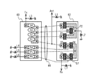
図1は、実施例1〜2に係るデュプレクサの回路図である。本実施例では、W−CDMA(Wideband Code Division Multiple Access)のBand2に使用されるデュプレクサ(送信帯域が1850〜1910MHz、受信帯域が1930〜1990MHz)を例に説明を行う。図1に示すように、アンテナ端子Antと送信端子Txとの間に送信フィルタ10が、アンテナ端子Antと受信端子Rxとの間に受信フィルタ12がそれぞれ接続されている。送信フィルタ10及び受信フィルタ12は、それぞれ直列共振子及び並列共振子がラダー状に接続されたラダーフィルタである。アンテナ端子Antは、送信フィルタ10及び受信フィルタ12で共有されており、アンテナ端子Antとグランドとの間には整合用のインダクタL1が接続されている。
FIG. 1 is a circuit diagram of a duplexer according to the first and second embodiments. In this embodiment, a duplexer (transmission band is 1850 to 1910 MHz and reception band is 1930 to 1990 MHz) used for
送信フィルタ10は、アンテナ端子Antと送信端子Txとの間に接続された直列共振子S1〜S4と、それぞれの直列共振子間に接続された並列共振子P1〜P3を含む。並列共振子P1〜P3の一端(直列共振子と接続された側と反対側)は共通化され、インダクタL2を介して接地されている。送信端子Txとグランドとの間には、整合用のインダクタL3が接続されている。
The
受信フィルタ12は、アンテナ端子Antと受信端子Rxとの間に接続された直列共振子S5〜S8と、それぞれの直列共振子間に接続された並列共振子P4〜P6を含む。並列共振子P4〜P6の一端(直列共振子と接続された側と反対側)は、それぞれ別個のインダクタL4〜L6を介して接地されている。受信端子Rxとグランドとの間には、整合用のインダクタL7が接続されている。
The
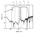
図2は、デュプレクサを構成する送信フィルタ10と受信フィルタ12のそれぞれの通過特性を示す図である。本実施例に係るBand2用のデュプレクサでは、受信フィルタ12の通過帯域(Rx)が送信フィルタ10の通過帯域(Tx)に比べ高い周波数帯にある。このため、送信フィルタ10の直列共振子S1〜S4及び受信フィルタ12の並列共振子P4〜P6が、送信フィルタ10と受信フィルタ12との間のガードバンド側におけるフィルタのスカート特性(符号20)を形成する。また、送信フィルタ10の並列共振子P1〜P3及び受信フィルタ12の直列共振子S5〜S8が、それぞれ上記ガードバンドと反対側におけるフィルタのスカート特性(符号22)を形成する。
FIG. 2 is a diagram illustrating pass characteristics of the
図1の直列共振子S1〜S8及び並列共振子P1〜P6には、例えば圧電薄膜共振子や弾性表面波共振子をはじめとする共振子を、機器の仕様等に応じて適宜用いることができる。本実施例では、ガードバンド側のスカート特性を形成する直列共振子S1〜S4及び並列共振子P4〜P6に、温度補償型の圧電薄膜共振子(TC−FBAR)を用いる。また、ガードバンドと反対側のスカート特性を形成する並列共振子P1〜P3及び直列共振子S5〜S8には、温度補償膜を含まない非温度補償型の圧電薄膜共振子(FBAR)を用いる。これらの二種類の圧電薄膜共振子は、以下に詳述するように、それぞれ圧電薄膜並びに当該圧電薄膜を挟んで対向する下部電極及び上部電極を含む複数の層から構成されている。 For the series resonators S1 to S8 and the parallel resonators P1 to P6 in FIG. 1, for example, a resonator including a piezoelectric thin film resonator and a surface acoustic wave resonator can be used as appropriate according to the specifications of the device. . In this embodiment, temperature compensated piezoelectric thin film resonators (TC-FBAR) are used for the series resonators S1 to S4 and the parallel resonators P4 to P6 that form the skirt characteristic on the guard band side. Further, non-temperature compensated piezoelectric thin film resonators (FBARs) that do not include a temperature compensation film are used for the parallel resonators P1 to P3 and the series resonators S5 to S8 that form the skirt characteristic opposite to the guard band. These two types of piezoelectric thin film resonators are each composed of a plurality of layers including a piezoelectric thin film and a lower electrode and an upper electrode facing each other across the piezoelectric thin film.
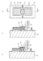
図3は、温度補償型の圧電薄膜共振子(TC−FBAR)の構成を示す図である。図3(a)はTC−FBARを上方向(上部電極側)から見た平面図であり、直列共振子S1〜S4及び並列共振子P4〜P6に共通の図である。図3(b)は受信フィルタ12の並列共振子P4〜P6の断面図、図3(c)は送信フィルタ10の直列共振子S1〜S4の断面図であり、それぞれ図3(a)のA−A線に沿った断面を示す図である。
FIG. 3 is a diagram showing a configuration of a temperature-compensated piezoelectric thin film resonator (TC-FBAR). FIG. 3A is a plan view of the TC-FBAR as viewed from above (upper electrode side), and is a view common to the series resonators S1 to S4 and the parallel resonators P4 to P6. 3B is a cross-sectional view of the parallel resonators P4 to P6 of the
図3(b)に示すように、受信フィルタ12の並列共振子P4〜P6では、基板30上に下部電極32が形成されており、下部電極32の一部が上方向(基板30と反対側)に凸状に湾曲することにより、ドーム状の空隙34が形成されている。更に、下部電極32のうち少なくとも上記の空隙34が形成された領域の一部を覆うように、基板30上に第1圧電薄膜36a、温度補償膜38、第2圧電薄膜36b、上部電極40、及びパシベーション膜42(以上、下部電極32からパシベーション膜42までを積層膜50と称する)が順に積層されている。これにより、上部電極40と下部電極32は、圧電薄膜(第1圧電薄膜36a及び第2圧電薄膜36b)の少なくとも一部を挟んで対向し、当該対向する領域における下部電極32の下方に空隙34を有する構成となっている。
As shown in FIG. 3B, in the parallel resonators P4 to P6 of the
図3(a)に示すように、上部電極40と下部電極32とが第1圧電薄膜36a及び第2圧電薄膜36bを挟んで対向する領域は、共振領域52となっている。共振領域52付近における下部電極32の表面には、エッチング媒体導入孔54が設けられている。また、エッチング媒体導入孔54と空隙34との間には、エッチング媒体導入路56が形成されている。また、下部電極32については、点線で示された全体部分のうち、圧電薄膜36の開口部から一部(斜線部)が露出する構成となっている。
As shown in FIG. 3A, a region where the
基板30としては、例えばシリコン(Si)を用いることができるが、他にもガラス、セラミック等を用いることができる。下部電極32としては、例えば基板30側からクロム(Cr)及びルテニウム(Ru)が順に積層された電極膜を用いることができる。上部電極40としては、例えば基板30側からルテニウム(Ru)及びクロム(Cr)が順に積層された電極膜を用いることができる(Ru層を符号40aで、Cr層を符号40bでそれぞれ図示する)。上記の他にも、下部電極32及び上部電極40には、他にもアルミニウム(Al)、銅(Cu)、モリブデン(Mo)、タングステン(W)、タンタル(Ta)、白金(Pt)、ロジウム(Rh)、イリジウム(Ir)等の金属層を組み合わせて用いることができる。また、電極膜を2層構造とせずに、1層構造とすることもできる。
For example, silicon (Si) can be used as the
第1圧電薄膜36a及び第2圧電薄膜36bとしては、例えば窒化アルミニウム(AlN)膜を用いることで、高Q値の圧電薄膜を安定して形成することができる。圧電薄膜としては、他にも酸化亜鉛(ZnO)、チタン酸ジルコン酸鉛(PZT)、チタン酸鉛(PbTiO3)等の圧電材を用いることができる。また、後述する電気機械結合係数k2 effを大きくするために、上記の圧電材を主成分とする圧電薄膜に、例えばスカンジウム(Sc)等の第3元素を添加し、圧電定数を増加させてもよい。ここで、「主成分とする」とは、窒化アルミニウム等の圧電材が圧電薄膜共振器の圧電薄膜として機能する程度に第3元素を含有する場合を含む。例えば、上記のようにQ値を高めるために圧電薄膜に第3元素(Mで表す)を添加する場合には、MxAl1−xNにおいて例えばx<0.5としてもよい。
As the first piezoelectric
温度補償膜38は、圧電薄膜(36a、36b)の弾性定数の温度係数とは逆符号の温度係数を有する膜であり、例えば二酸化珪素(SiO2)を用いることができるが、他にも酸化シリコンまたは窒化シリコンを主成分とする膜を用いることができる。すなわち、温度補償膜38が圧電薄膜共振子における温度補償効果を有する範囲において、温度補償膜38の共振周波数の温度係数を大きくする第3元素を添加してもよい。温度補償膜38は、下部電極32及び上部電極40の外側に配置することも可能であるが、下部電極32と上部電極40との間に配置した方が、温度補償膜38の厚みを小さくすることができるため好ましい。
The
パシベーション膜42としては、例えば二酸化珪素(SiO2)を用いることができるが、他にも窒化アルミニウム(AlN)等の別の絶縁材料を用いることができる。
As the
上述の積層膜50は、例えばスパッタリング法等により成膜を行い、フォトリソグラフィー技術及びエッチング技術により所望の形状にパターニングすることで形成することができる。また、積層膜50のパターニングは、リフトオフ技術により行うこともできる。第1圧電薄膜36a、温度補償膜38、及び第2圧電薄膜36bの外周のエッチングは、例えば上部電極40をマスクとしたウェットエッチングにより行うことができる。
The
下部電極32の下方に位置するドーム状の空隙34は、下部電極32を形成する前に予め設けられていた犠牲層(不図示)を、上述の積層膜50の形成後に除去することにより形成することができる。犠牲層には、例えばMgO、ZnO、Ge、SiO2等の、エッチング液またはエッチングガスにより容易に溶解することができる材料を用いることができ、例えばスパッタリング法または蒸着法等により形成することができる。犠牲層は、フォトリソグラフィー技術及びエッチング技術により、予め所望の形(空隙34の形状)に成形される。積層膜50の形成後は、下部電極32に形成されたエッチング媒体導入孔54及びエッチング媒体導入路56を介して、下部電極32の下にエッチング媒体を導入することにより、犠牲層の除去を行う。なお、空隙34は、基板30を貫通するように形成してもよく、当該空隙34を介して下部電極32の下面が外部に露出する構成としてもよい。
The dome-shaped
図3(c)に示すように、送信フィルタ10の直列共振子S1〜S4の構成は、図3(b)の並列共振子P4〜P6とほぼ同様であるが、上部電極40におけるRu層40aとCr層40bとの間に、共振周波数調整用の付加膜44が形成されている点が異なる。直列共振子S1〜S4は、付加膜44を備えることにより、並列共振子P4〜P6に比べて共振周波数が低周波側にシフトされている。付加膜44としては、チタン(Ti)を用いることができるが、他にもアルミニウム(Al)、銅(Cu)、クロム(Cr)、モリブデン(Mo)、タングステン(W)、タンタル(Ta)、白金(Pt)、ルテニウム(Ru)、ロジウム(Rh)、イリジウム(Ir)、二酸化珪素(SiO2)等を用いることができる。
As shown in FIG. 3C, the configuration of the series resonators S1 to S4 of the
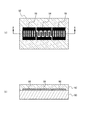
図4は、温度補償膜を含まない非温度補償型の圧電薄膜共振子(FBAR)の構成を示す図である。図3と共通する構成要素については同一の符号を付し、詳細な説明を省略する。図4(a)はFBARを上方向から見た平面図であり、並列共振子P1〜P3及び直列共振子S5〜S8に共通の図である。図4(b)は受信フィルタ12の直列共振子S5〜S8の断面図、図4(c)は送信フィルタ10の並列共振子P1〜P3の断面図であり、それぞれ図4(a)のA−A線に沿った断面を示す図である。
FIG. 4 is a diagram showing a configuration of a non-temperature compensation type piezoelectric thin film resonator (FBAR) that does not include a temperature compensation film. Constituent elements common to those in FIG. 3 are denoted by the same reference numerals, and detailed description thereof is omitted. FIG. 4A is a plan view of the FBAR as viewed from above, and is common to the parallel resonators P1 to P3 and the series resonators S5 to S8. 4B is a cross-sectional view of the series resonators S5 to S8 of the
図4(b)に示すように、受信フィルタ12の直列共振子S5〜S8は、温度補償膜38を含まない点を除き、図3(b)に示す受信フィルタ12の並列共振子P4〜P6の構成と同様である。また、図4(c)に示すように、送信フィルタ10の並列共振子P1〜P3は、温度補償膜38を含まない点を除き、図3(c)に示す送信フィルタ10の直列共振子S1〜S4の構成と同様である。上記の非温度補償型のFBARでは、温度補償膜38が存在しないため、TC−FBARと異なり圧電薄膜36は2つに分離されていない。
4B, the series resonators S5 to S8 of the
図5は、実施例1に係るデュプレクサのレイアウトを示す平面模式図である。直列共振子S1〜S8、並列共振子P1〜P6、及びインダクタL1〜L7は、それぞれ図1に示す回路素子に対応する。図中にクロスハッチで示した領域64は、上記の共振子及びインダクタに接続された配線パターンを示す。図示するように、TC−FBAR型の直列共振子S1〜S4及び並列共振子P4〜P6が、同一の第1チップ60に形成されている。非温度補償型のFBAR型の並列共振子P1〜P3及び直列共振子S5〜S8は、同一の第2チップ62に形成されている。また、異なるチップである第1チップ60及び第2チップ62間における共振子同士の接続(図中の領域66)は、以下に説明するように、チップが実装される実装基板上の表面に形成された配線を介して互いに接続されている。
FIG. 5 is a schematic plan view illustrating the layout of the duplexer according to the first embodiment. The series resonators S1 to S8, the parallel resonators P1 to P6, and the inductors L1 to L7 correspond to the circuit elements shown in FIG. A
図6は、実施例1に係るデュプレクサのレイアウトを示す断面模式図である。実装基板70は、複数の基板(70a〜70c)が積層された積層基板であり、表面に第1チップ60及び第2チップ62が、バンプ68を介してフリップチップにより実装されている。実装基板70の各層の主面には、それぞれ配線パターン72が形成されており、異なる層の配線パターン72同士は、実装基板70に形成されたビア74を介して互いに接続されている。第1チップ60及び第2チップ62は、実装基板70の表面のダイアタッチ層(70c)上に形成された配線パターン(符号66で図示)を介して、互いに電気的に接続されている。より詳細には、送信フィルタ10に含まれる直列共振子S1〜S4及び並列共振子P1〜P3同士、並びに受信フィルタ12に含まれる直列共振子S5〜S8及び並列共振子P4〜P6同士が、上記ダイアタッチ層70c上に形成された配線を介して、互いに電気的に接続されている。これにより、第1チップ60及び第2チップ62を実装基板70内部の配線パターンを介して接続する場合に比べ、配線のインダクタンス成分を低減し、フィルタ特性への影響を抑制することができる。
FIG. 6 is a schematic cross-sectional view illustrating the layout of the duplexer according to the first embodiment. The mounting substrate 70 is a laminated substrate in which a plurality of substrates (70a to 70c) are laminated, and the
ここで、図2のようにガードバンドの狭いデュプレクサでは、フィルタにおけるガードバンド側のスカート特性は急峻であることが好ましく、且つフィルタの温度安定性も良好であることが好ましい。スカート特性の急峻化は、電気機械結合係数k2 effを小さくすることにより、温度安定性の向上は、周波数温度係数TCFを小さくすることによりそれぞれ実現することができる。従って、ガードバンド側のスカート特性を形成する直列共振子S1〜S4及び並列共振子P4〜P6(共に第1チップ60に形成される)は、電気機械結合係数k2 eff及び周波数温度係数TCFが小さくなるようにすることが好ましい。 Here, in a duplexer having a narrow guard band as shown in FIG. 2, the skirt characteristic on the guard band side of the filter is preferably steep, and the temperature stability of the filter is also preferably good. The steep skirt characteristic can be realized by reducing the electromechanical coupling coefficient k 2 eff, and the improvement in temperature stability can be realized by reducing the frequency temperature coefficient TCF. Therefore, the series resonators S1 to S4 and the parallel resonators P4 to P6 (both formed on the first chip 60) forming the skirt characteristic on the guard band side have an electromechanical coupling coefficient k 2 eff and a frequency temperature coefficient TCF. It is preferable to make it smaller.
一方、ガードバンドと反対側のスカート特性は、ガードバンド側に比べ急峻性及び温度安定性がそれほど要求されない代わりに、フィルタの通過帯域がなるべく広くなるように設定されることが好ましい。帯域幅の拡大は、k2 effを大きくすることにより達成することができるが、これはスカート特性の急峻化とはトレードオフの関係にある。従って、ガードバンドと反対側のスカート特性を形成する並列共振子P1〜P3及び直列共振子S5〜S8(共に第2チップ62に形成される)においては、k2 effが大きくなるようにすることが好ましい。 On the other hand, the skirt characteristic on the side opposite to the guard band is preferably set so that the pass band of the filter is as wide as possible, instead of requiring steepness and temperature stability less than the guard band side. Bandwidth expansion can be achieved by increasing k 2 eff , which is in a trade-off relationship with steep skirt characteristics. Therefore, in the parallel resonators P1 to P3 and the series resonators S5 to S8 (both formed on the second chip 62) that form the skirt characteristic opposite to the guard band, k 2 eff is increased. Is preferred.
次に、実施例1に係るデュプレクサのフィルタ特性について、比較例に係るデュプレクサと比較したシミュレーション結果について説明する。 Next, the simulation result compared with the duplexer which concerns on the duplexer which concerns on the duplexer which concerns on the duplexer which concerns on Example 1 is demonstrated.
図7は、シミュレーションに用いた積層膜50の具体的な材質及び膜厚を示す図である。受信フィルタ12の並列共振子P4〜P6(RxP、図3(b))では、下部電極32を膜厚85nmのCr及び膜厚195nmのRuの2層構造(基板30側がCr)、第1圧電薄膜36aを膜厚555nmのAlN、温度補償膜38を膜厚70nmのSiO2、第2圧電薄膜36bを膜厚555nmのAlN、上部電極を膜厚195nmのRu(40a)及び膜厚25nmのCr(40b)の2層構造、パシベーション膜42を膜厚20nmのSiO2とした。送信フィルタ10の直列共振子S1〜S4(TxS、図3(c))では、上記の膜厚構成に加え、上部電極のRu層40aとCr層40bとの間に形成される付加膜44を、膜厚40nmのTiとした。
FIG. 7 is a diagram showing specific materials and film thicknesses of the
受信フィルタ12の直列共振子S5〜S8(RxS、図4(b))では、下部電極32を膜厚100nmのCr及び膜厚210nmのRuの2層構造(基板30側がCr)、圧電薄膜36を膜厚1220nmのAlN、上部電極を膜厚210nmのRu(40a)及び膜厚30nmのCr(40b)の2層構造、パシベーション膜42を膜厚20nmのSiO2とした。送信フィルタ10の並列共振子P1〜P3(TxP、図4(c))では、上記の膜厚構成に加え、上部電極のRu層40aとCr層40bとの間に形成される付加膜44を、膜厚155nmのTiとした。
In the series resonators S5 to S8 (RxS, FIG. 4B) of the
ガードバンド(GB)側のスカート特性を形成する2組の共振子(P4〜P6及びS1〜S4)を比較すると、付加膜44を除く他の積層膜の材質及び膜厚は全て同一である。ガードバンド(GB)側と反対側のスカート特性を形成する2組の共振子(S5〜S8及びP1〜P3)においても、付加膜44を除く他の積層膜の材質及び膜厚は全て同一である。また、付加膜44の形成に伴う並列共振子P1〜P3における周波数シフト量は、直列共振子S1〜S4における同様の周波数シフト量より大きい。従って、付加膜44の膜厚は、P1〜P3(155nm)の方がS1〜S4(40nm)に比べて大きくなっている。
Comparing the two sets of resonators (P4 to P6 and S1 to S4) that form the skirt characteristics on the guard band (GB) side, the materials and film thicknesses of the other laminated films excluding the
比較例に係るデュプレクサでは、デュプレクサを構成する全ての共振子を、圧電薄膜の中央に温度補償膜を挿入したTC−FBAR型の圧電膜膜共振子とした。その具体的な形態は、図3(a)〜(c)に示したものと同様である。 In the duplexer according to the comparative example, all the resonators constituting the duplexer are TC-FBAR type piezoelectric film resonators in which a temperature compensation film is inserted in the center of the piezoelectric thin film. The specific form is the same as that shown in FIGS.
実施例1では、ガードバンド側のスカート特性を形成する直列共振子S1〜S4及び並列共振子P4〜P6において、k2 effを約4.5%、TCFを約0ppm/℃とした。また、ガードバンド側と反対側のスカート特性を形成する並列共振子P1〜P3及び直列共振子S5〜S8において、k2 effを約7%、TCFを約−30ppm/℃とした。これに対し、比較例では、ガードバンド側及びその反対側の双方において、TC−FBAR型共振子の使用を想定し、スカート特性を形成する共振子のk2 effは約4.5%となっている。 In Example 1, in the series resonators S1 to S4 and the parallel resonators P4 to P6 that form the skirt characteristics on the guard band side, k 2 eff was about 4.5% and TCF was about 0 ppm / ° C. Further, in the parallel resonators P1 to P3 and the series resonators S5 to S8 forming the skirt characteristic on the side opposite to the guard band side, k 2 eff was about 7% and TCF was about −30 ppm / ° C. In contrast, in the comparative example, it is assumed that the TC-FBAR type resonator is used on both the guard band side and the opposite side, and the k 2 eff of the resonator forming the skirt characteristic is about 4.5%. ing.
図8は、実施例1に係るデュプレクサのフィルタ特性について、比較例との比較を示したグラフである。図8(a)は送信フィルタ10の帯域の通過特性、図8(b)は送信端子Txにおける帯域のリターンロス特性をそれぞれ示す。ガードバンド側のスカート特性を形成する共振子のk2 effは、実施例1と比較例で共に約4.5%であるため、スカート特性にもそれほど大きな差はない。これに対し、ガードバンドと反対側のスカート特性を形成する共振子のk2 effは、比較例では4.5%であるのに対し、実施例1では7%となっている。このため、実施例1では、比較例に比べてマッチングが改善し、フィルタの広帯域化が図られている。
FIG. 8 is a graph showing a comparison with the comparative example regarding the filter characteristics of the duplexer according to the first embodiment. FIG. 8A shows the band pass characteristic of the
以上のように、実施例1に係るデュプレクサによれば、送信フィルタ10と受信フィルタ12の間のガードバンド側のスカート特性を形成する複数の共振子S1〜S4及びP4〜P6(以下、「第1共振子」とする)は、温度補償型の圧電薄膜共振子(TC−TBAR)となっている。また、ガードバンドと反対側のスカート特性を形成する複数の共振子P1〜P3及びS5〜S8(以下、「第2共振子」とする)は、温度補償膜38を含まない非温度補償型の圧電薄膜共振子(FBAR)となっている。このように、実施例1に係るデュプレクサによれば、第1共振子にはk2 eff及びTCFの小さい共振子を用い、第2共振子には第1共振子に比べてk2 eff及びTCFの大きい共振子を用いている。これにより、ガードバンド側のスカート特性の急峻化及び温度安定性の向上と、フィルタの広帯域化との両立を図ることができる。
As described above, according to the duplexer according to the first embodiment, the plurality of resonators S1 to S4 and P4 to P6 (hereinafter referred to as “first”) that form the skirt characteristics on the guard band side between the
実施例2は、第2共振子にFBAR以外の共振子を用いる例である。 The second embodiment is an example in which a resonator other than the FBAR is used as the second resonator.
図9は、実施例2に係るデュプレクサのレイアウトを示す平面図である。実施例1(図5)と比較すると、ガードバンドと反対側のスカート特性を形成する並列共振子P1〜P3及び直列共振子S5〜S8の形態が、弾性表面波(SAW)共振子となっている。その他の構成は実施例1と同じであり、詳細な説明を省略する。 FIG. 9 is a plan view illustrating the layout of the duplexer according to the second embodiment. Compared with Example 1 (FIG. 5), the forms of the parallel resonators P1 to P3 and the series resonators S5 to S8 that form the skirt characteristics opposite to the guard band are surface acoustic wave (SAW) resonators. Yes. Other configurations are the same as those of the first embodiment, and detailed description thereof is omitted.
図10〜図12は、様々な形態のSAW共振子の構成を示す図である。図10(a)、図11(a)、図12(a)は平面模式図、図10(b)、図11(b)、図12(b)は上記平面模式図のA−A線に沿った断面模式図である。図10に示す弾性表面波共振子(以下、「LT/Sa型弾性表面波共振子」とする)は、42°YカットX伝播のタンタル酸リチウム(LiTaO3)基板80をサファイア基板82の上に貼り付けた基板を用い、当該基板上に櫛形電極84及び反射電極86を形成したものである。タンタル酸リチウム基板80の厚みは例えば20μm、サファイア基板82の厚みは例えば230μmとすることができる。また、櫛形電極84及び反射電極86の電極材料には、例えば主成分のAlにCuを添加した金属を用いることができる。以上のLT型弾性表面波共振子において、k2 effは約8%、TCFは約−20ppm/℃である。
10 to 12 are diagrams showing configurations of various forms of SAW resonators. 10 (a), 11 (a), and 12 (a) are schematic plan views, and FIGS. 10 (b), 11 (b), and 12 (b) are taken along line AA of the above schematic plan view. It is the cross-sectional schematic diagram along. A surface acoustic wave resonator shown in FIG. 10 (hereinafter referred to as an “LT / Sa type surface acoustic wave resonator”) is a 42 ° Y-cut X-propagation lithium tantalate (LiTaO 3 )
図11に示す弾性表面波共振子(以下、「LT型弾性表面波共振子」とする)は、基板としてサファイア基板を用いずに、42°YカットX伝播のタンタル酸リチウム(LiTaO3)基板80を用いた例であり、その他の構成は図10と同様である。上記のLT型弾性表面波共振子において、k2 effは約8%、TCFは約−40ppm/℃とすることができる。 The surface acoustic wave resonator shown in FIG. 11 (hereinafter referred to as “LT type surface acoustic wave resonator”) does not use a sapphire substrate as a substrate, but a 42 ° Y-cut X-propagation lithium tantalate (LiTaO 3 ) substrate. 80 is an example, and other configurations are the same as those in FIG. In the above-described LT type surface acoustic wave resonator, k 2 eff can be about 8% and TCF can be about −40 ppm / ° C.
図12に示す弾性表面波共振子(以下、「ラブ波型弾性表面波共振子」とする)は、基板として0°YカットX伝播のニオブ酸リチウム(LiNbO3)基板90を用いたラブ波利用の弾性表面波共振子である。ニオブ酸リチウム基板90上には、図10及び図11と同様に櫛形電極84及び反射電極86が形成され、これらの電極を含む基板上面全体が、シリコン酸化膜92により覆われている。櫛形電極84及び反射電極86の電極材料としては、例えばCuを主成分とする金属を用いることができる。上記のラブ波型弾性表面波共振子において、k2 effは約11%、TCFは約0ppm/℃とすることができる。
A surface acoustic wave resonator (hereinafter referred to as a “love wave type surface acoustic wave resonator”) shown in FIG. 12 uses a 0 ° Y-cut X-propagation lithium niobate (LiNbO 3 )
次に、実施例2に係るデュプレクサのフィルタ特性について、比較例に係るデュプレクサと比較したシミュレーション結果について説明する。実施例2では、ガードバンド側のスカート特性を形成する直列共振子S1〜S4及び並列共振子P4〜P6においては、実施例1と同じくTC−FBAR型共振子の使用を想定し、k2 effを約4.5%、TCFを約0ppm/℃とした。また、ガードバンド側と反対側のスカート特性を形成する並列共振子P1〜P3及び直列共振子S5〜S8においては、LT/Sa型弾性表面波共振子の使用を想定し、k2 effを約8%、TCFを約−20ppm/℃とした。これに対し、比較例では、実施例1の場合と同じく、ガードバンド側及びその反対側の双方において、TC−FBAR型共振子の使用を想定し、スカート特性を形成する共振子のk2 effを約4.5%とした。 Next, simulation results of the filter characteristics of the duplexer according to the second embodiment compared with the duplexer according to the comparative example will be described. In the second embodiment, the series resonators S1 to S4 and the parallel resonators P4 to P6 that form the skirt characteristics on the guard band side are assumed to use TC-FBAR type resonators as in the first embodiment, and k 2 eff Was about 4.5% and TCF was about 0 ppm / ° C. In parallel resonators P1 to P3 and series resonators S5 to S8 that form a skirt characteristic opposite to the guard band, it is assumed that an LT / Sa type surface acoustic wave resonator is used, and k 2 eff is about 8%, TCF was about -20 ppm / ° C. On the other hand, in the comparative example, as in the case of the first embodiment, it is assumed that the TC-FBAR type resonator is used on both the guard band side and the opposite side, and the k 2 eff of the resonator that forms the skirt characteristic is assumed. About 4.5%.
図13は、実施例2に係るデュプレクサのフィルタ特性について、比較例との比較を示したグラフである。図13(a)は送信フィルタ10の帯域の通過特性、図13(b)は送信端子Txにおける帯域のリターンロス特性をそれぞれ示す。ガードバンド側のスカート特性を形成する共振子のk2 effは、実施例2と比較例で共に約4.5%であるため、スカート特性にもそれほど大きな差はない。これに対し、ガードバンドと反対側のスカート特性を形成する共振子のk2 effは、比較例では4.5%であるのに対し、実施例2では8%となっている。このため、実施例2では、比較例に比べてマッチングが改善し、フィルタの広帯域化が図られている。
FIG. 13 is a graph showing a comparison with the comparative example regarding the filter characteristics of the duplexer according to the second embodiment. FIG. 13A shows the band pass characteristic of the
以上のように、実施例2に係るデュプレクサによれば、送信フィルタ10と受信フィルタ12の間のガードバンド側のスカート特性を形成する複数の第1共振子(S1〜S4及びP4〜P6)は、温度補償型圧電薄膜共振子(TC−TBAR)となっている。また、ガードバンドと反対側のスカート特性を形成する複数の第2共振子(P1〜P3及びS5〜S8)は、タンタル酸リチウム基板を用いたLT型弾性表面波共振子、タンタル酸リチウム基板をサファイア基板上に貼り付けた基板を用いたLT/Sa型弾性表面波共振子、または弾性表面波共振子のうちラブ波を利用したラブ波型弾性表面波共振子となっている。このように、実施例2に係るデュプレクサによれば、実施例1と同様に、第1共振子にはk2 eff及びTCFの小さい共振子を用い、第2共振子には第1共振子に比べてk2 eff及びTCFの大きい共振子を用いている。これにより、ガードバンド側のスカート特性の急峻化及び温度安定性の向上と、フィルタの広帯域化との両立を図ることができる。
As described above, according to the duplexer according to the second embodiment, the plurality of first resonators (S1 to S4 and P4 to P6) that form the skirt characteristic on the guard band side between the
上記の例において、貼り合わせ基板を用いたLT/Sa型弾性表面波共振子は、タンタル酸リチウム基板のみを用いたLT型弾性表面波共振子に比べ、TCFが小さく温度安定性に優れている。また、ラブ波を利用したラブ波型弾性表面波共振子は、k2 effが大きく広帯域化に有利で、且つTCFが小さく温度安定性に優れた弾性表面波共振子となっている。 In the above example, the LT / Sa type surface acoustic wave resonator using the bonded substrate has a smaller TCF and excellent temperature stability than the LT type surface acoustic wave resonator using only the lithium tantalate substrate. . A Love wave type surface acoustic wave resonator using a Love wave is a surface acoustic wave resonator which has a large k 2 eff and is advantageous for widening the band and has a small TCF and excellent temperature stability.
実施例1〜2では、ガードバンド側の第1共振子として温度補償型圧電薄膜共振子を用いたが、代わりに図12に示すラブ波型弾性表面波共振子を用いてもよい。このとき、ガードバンドと反対側の第2共振子にもラブ波型弾性表面波共振子を用いる場合には、第2共振子の電気機械結合係数k2 effを第1共振子より大きくする。このとき、k2 effの小さい第1共振子を第1ラブ波型弾性表面波共振子、k2 effの大きい第2共振子を第2ラブ波型弾性表面波共振子とそれぞれ称する。ガードバンド側のスカート特性を形成する第1ラブ波型弾性表面波共振子は、実施例1〜2にて示した第2共振子の実施例のいずれとも組み合わせることができる。 In Examples 1 and 2, the temperature compensated piezoelectric thin film resonator is used as the first resonator on the guard band side, but a Love wave type surface acoustic wave resonator shown in FIG. 12 may be used instead. At this time, when the Love wave type surface acoustic wave resonator is used for the second resonator opposite to the guard band, the electromechanical coupling coefficient k 2 eff of the second resonator is made larger than that of the first resonator. At this time, the first resonator having a small k 2 eff is referred to as a first Love wave type surface acoustic wave resonator, and the second resonator having a large k 2 eff is referred to as a second Love wave type surface acoustic wave resonator. The first love wave type surface acoustic wave resonator that forms the skirt characteristic on the guard band side can be combined with any of the second resonator embodiments shown in the first and second embodiments.
実施例1〜2では、第1共振子の電気機械結合係数k2 effは第2共振子のk2 effより小さく、第1共振子の周波数温度係数TCFは第2共振子のTCFより小さくなっているが、必ずしも全ての共振子において、上記の関係が満たされていなくともよい。例えば、送信フィルタ及び受信フィルタの少なくとも一方において、第1共振子のうち少なくとも1つのk2 effが、第2共振子のうち少なくとも1つのk2 effより小さくなっていればよい。また、送信フィルタ及び前記受信フィルタの少なくとも一方において、ガードバンド側におけるフィルタのTCFが、ガードバンドと反対側におけるフィルタのTCFより小さくなっていればよい。 In Examples 1-2, the electromechanical coupling coefficient k 2 eff of the first resonator is less than k 2 eff of the second resonator, the temperature coefficient of frequency TCF of the first resonator is smaller than the TCF of the second resonator However, the above relationship does not necessarily have to be satisfied in all the resonators. For example, in at least one of the transmission filter and the reception filter, it is sufficient that at least one k 2 eff of the first resonator is smaller than at least one k 2 eff of the second resonator. In addition, in at least one of the transmission filter and the reception filter, the TCF of the filter on the guard band side may be smaller than the TCF of the filter on the side opposite to the guard band.
また、実施例1〜2では、第1共振子(S1〜S4及びP4〜P6)の全てを第1チップ60上に形成し、第2共振子(P1〜P3及びS5〜S8)の全てを第1チップ60とは別の第2チップ62上に形成したが、共振子の構成はこれ以外の形態であってもよい。例えば、第2共振子のうちS5〜S8を同一チップに形成し、P1〜P3を別のチップに形成するなどしてもよい。
In the first and second embodiments, all of the first resonators (S1 to S4 and P4 to P6) are formed on the
ただし、共振子を同一チップに形成する場合、同一のウェハ及び同一のプロセス(素子技術)により共振子の形成を行うことができる。これにより、別々のウェハに別々のプロセスにより共振子の形成を行う場合に比べ、膜厚の調整を容易に行うことができる。例えば、図7に示すように、第1共振子のうちS1〜S4とP4〜P6とでは、1つの層(ここでは、膜厚調整が必要な付加膜44(Ti))を除く全ての積層膜50の膜厚が等しく、これらを同一工程で形成することができる。これにより、共振子の周波数特性を揃え、送信フィルタと受信フィルタのそれぞれのスカート特性における周波数間隔のばらつきを抑制することができる。Band2のようにガードバンドの狭いデュプレクサにでは、ガードバンド側における周波数特性の安定が特に要求されるため、ガードバンド側の第1共振子は同一のチップに形成することが特に好ましい。また、ガードバンドと反対側の第2共振子においても、第1共振子と同様に同一のチップに形成することが好ましい。
However, when the resonator is formed on the same chip, the resonator can be formed by the same wafer and the same process (element technology). Thereby, the film thickness can be easily adjusted as compared with the case where the resonator is formed on different wafers by different processes. For example, as shown in FIG. 7, in the first resonator, S1 to S4 and P4 to P6 are all stacked except one layer (here, the additional film 44 (Ti) that needs to be adjusted). The thicknesses of the
また、第1共振子及び第2共振子の全てを同一のチップに形成してもよい。この場合、k2 eff及びTCFの異なる二種類の共振子を同一のチップに形成することとなるため、製造工程における工夫が要求される。上記のようなデュプレクサの形成方法としては、例えば最初にチップ上の所定領域に第1共振子の形成を行い、続いて形成済みの第1共振子の上にマスクを施した上で、チップ上の残りの領域に第2共振子の形成を行う方法が考えられる。 Further, all of the first resonator and the second resonator may be formed on the same chip. In this case, since two types of resonators having different k 2 eff and TCF are formed on the same chip, a device in the manufacturing process is required. As a method of forming the duplexer as described above, for example, first the first resonator is formed in a predetermined region on the chip, and then a mask is applied on the formed first resonator, and then the chip is formed on the chip. A method of forming the second resonator in the remaining region is conceivable.
実施例1〜2では、例えば図3及び図4に示すように、圧電薄膜共振子として下部電極32の下に空隙34が形成されたFBARタイプを例に説明を行ったが、圧電薄膜共振子は温度補償膜を用いるSMRタイプとしてもよい。音響反射膜とは、音響インピーダンスの高い膜と低い膜とが交互にλ/4(λは弾性波の波長)の膜厚で積層された膜であり、下部電極32の下に空隙34に代えて形成することができる。よって、実施例1〜2における温度補償型圧電薄膜共振子は、FBARタイプの圧電薄膜共振子に温度補償膜が挿入された構成に加え、SMRタイプの圧電薄膜共振子に温度補償膜が挿入された形態を含むものとする。
In Examples 1 and 2, for example, as shown in FIGS. 3 and 4, the FBAR type in which a
また、実施例1〜2では、送信フィルタ及び受信フィルタとして図1に示すラダーフィルタを例に説明したが、ラダーフィルタの具体的構成(直列共振子・並列共振子の数及び配置)は、これに限定されるものではない。整合用インダクタの数及び配置についても、デュプレクサの仕様等に応じて適宜変更することができる。 In the first and second embodiments, the ladder filter illustrated in FIG. 1 is described as an example of the transmission filter and the reception filter. However, the specific configuration of the ladder filter (the number and arrangement of series resonators and parallel resonators) It is not limited to. The number and arrangement of matching inductors can be changed as appropriate according to the specifications of the duplexer.
また、実施例1〜2では、低周波側に送信フィルタが、高周波側に受信フィルタがあるデュプレクサを例に説明したが、低周波側に受信フィルタ12が、高周波側に送信フィルタがあってもよい。また、上記実施例ではBand2用のデュプレクサを例に説明したが、上記実施例の構成はこれ以外の周波数帯域を対象とするデュプレクサにおいても同様に適用することができる。
In the first and second embodiments, a duplexer having a transmission filter on the low frequency side and a reception filter on the high frequency side is described as an example. However, even if the
以上、本発明の実施例について詳述したが、本発明はかかる特定の実施例に限定されるものではなく、特許請求の範囲に記載された本発明の要旨の範囲内において、種々の変形・変更が可能である。 Although the embodiments of the present invention have been described in detail above, the present invention is not limited to such specific embodiments, and various modifications and changes can be made within the scope of the gist of the present invention described in the claims. It can be changed.
10 送信フィルタ
12 受信フィルタ
30 基板
32 下部電極
34 空隙
36 圧電薄膜
38 温度補償膜
40 上部電極
42 パシベーション膜
44 付加膜
50 積層膜
52 共振領域
54 エッチング媒体導入孔
56 エッチング媒体導入路
60 第1チップ
62 第2チップ
64、66、72 配線パターン
68 バンプ
70 実装基板
74 ビア
80 タンタル酸リチウム基板
82 サファイア基板
84 櫛形電極
86 反射電極
90 ニオブ酸リチウム基板
92 シリコン酸化膜
Ant アンテナ端子
Tx 送信端子
Rx 受信端子
S1〜S8 直列共振子
P1〜P6 並列共振子
L1〜L7 インダクタ
DESCRIPTION OF
Claims (11)
前記送信フィルタ及び前記受信フィルタは、それぞれラダー状に接続された直列共振子及び並列共振子を含み、
前記一方のフィルタの前記直列共振子と前記他方のフィルタの前記並列共振子が第1共振子として第1チップに形成され、前記一方のフィルタの前記並列共振子と前記他方のフィルタの前記直列共振子が第2共振子として前記第1チップとは異なる第2チップに形成され、
前記第1共振子は圧電薄膜並びに前記圧電薄膜を挟んで対向する下部電極及び上部電極を含む複数の層からなり且つ前記圧電薄膜の弾性定数の温度係数と逆符号の温度係数を有する温度補償膜が前記上部電極と前記下部電極との間に挟まれた温度補償型圧電薄膜共振子であり、前記第2共振子は圧電薄膜並びに前記圧電薄膜を挟んで対向する下部電極及び上部電極を含む複数の層からなり且つ前記上部電極と前記下部電極との間に挟まれた温度補償膜を含まない非温度補償型圧電薄膜共振子であることを特徴とするデュプレクサ。 A duplexer comprising the transmission filter and the reception filter whose pass band of any one of the transmission filter and the reception filter is lower than the pass band of the other filter of the transmission filter and the reception filter,
The transmission filter and the reception filter each include a series resonator and a parallel resonator connected in a ladder shape,
The series resonator of the one filter and the parallel resonator of the other filter are formed as a first resonator on a first chip, and the series resonator of the one filter and the series resonance of the other filter are formed. A child formed as a second resonator on a second chip different from the first chip ;
The first resonator includes a piezoelectric thin film and a plurality of layers including a lower electrode and an upper electrode facing each other with the piezoelectric thin film interposed therebetween, and has a temperature coefficient having a temperature coefficient opposite to the temperature coefficient of the elastic constant of the piezoelectric thin film. Is a temperature-compensated piezoelectric thin film resonator sandwiched between the upper electrode and the lower electrode, and the second resonator includes a piezoelectric thin film and a plurality of lower and upper electrodes facing each other with the piezoelectric thin film interposed therebetween. A duplexer characterized in that it is a non-temperature compensated piezoelectric thin film resonator that is composed of the above-mentioned layers and does not include a temperature compensation film sandwiched between the upper electrode and the lower electrode .
前記送信フィルタ及び前記受信フィルタは、それぞれラダー状に接続された直列共振子及び並列共振子を含み、
前記一方のフィルタの前記直列共振子と前記他方のフィルタの前記並列共振子が第1共振子として第1チップに形成され、前記一方のフィルタの前記並列共振子と前記他方のフィルタの前記直列共振子が第2共振子として前記第1チップとは異なる第2チップに形成され、
前記第1共振子は圧電薄膜並びに前記圧電薄膜を挟んで対向する下部電極及び上部電極を含む複数の層からなり且つ前記圧電薄膜の弾性定数の温度係数と逆符号の温度係数を有する温度補償膜が前記上部電極と前記下部電極との間に挟まれた温度補償型圧電薄膜共振子であり、前記第2共振子はタンタル酸リチウム基板を用いたLT型弾性表面波共振子であることを特徴とするデュプレクサ。 A duplexer comprising the transmission filter and the reception filter whose pass band of any one of the transmission filter and the reception filter is lower than the pass band of the other filter of the transmission filter and the reception filter,
The transmission filter and the reception filter each include a series resonator and a parallel resonator connected in a ladder shape,
The series resonator of the one filter and the parallel resonator of the other filter are formed as a first resonator on a first chip, and the series resonator of the one filter and the series resonance of the other filter are formed. A child formed as a second resonator on a second chip different from the first chip;
The first resonator includes a piezoelectric thin film and a plurality of layers including a lower electrode and an upper electrode facing each other with the piezoelectric thin film interposed therebetween, and has a temperature coefficient having a temperature coefficient opposite to the temperature coefficient of the elastic constant of the piezoelectric thin film. Is a temperature compensated piezoelectric thin film resonator sandwiched between the upper electrode and the lower electrode, and the second resonator is an LT type surface acoustic wave resonator using a lithium tantalate substrate. Duplexer .
前記送信フィルタ及び前記受信フィルタは、それぞれラダー状に接続された直列共振子及び並列共振子を含み、
前記一方のフィルタの前記直列共振子と前記他方のフィルタの前記並列共振子が第1共振子として第1チップに形成され、前記一方のフィルタの前記並列共振子と前記他方のフィルタの前記直列共振子が第2共振子として前記第1チップとは異なる第2チップに形成され、
前記第1共振子は圧電薄膜並びに前記圧電薄膜を挟んで対向する下部電極及び上部電極を含む複数の層からなり且つ前記圧電薄膜の弾性定数の温度係数と逆符号の温度係数を有する温度補償膜が前記上部電極と前記下部電極との間に挟まれた温度補償型圧電薄膜共振子であり、前記第2共振子はタンタル酸リチウム基板をサファイア基板上に貼り付けた基板を用いたLT/Sa型弾性表面波共振子であることを特徴とするデュプレクサ。 A duplexer comprising the transmission filter and the reception filter whose pass band of any one of the transmission filter and the reception filter is lower than the pass band of the other filter of the transmission filter and the reception filter,
The transmission filter and the reception filter each include a series resonator and a parallel resonator connected in a ladder shape,
The series resonator of the one filter and the parallel resonator of the other filter are formed as a first resonator on a first chip, and the series resonator of the one filter and the series resonance of the other filter are formed. A child formed as a second resonator on a second chip different from the first chip;
The first resonator includes a piezoelectric thin film and a plurality of layers including a lower electrode and an upper electrode facing each other with the piezoelectric thin film interposed therebetween, and has a temperature coefficient having a temperature coefficient opposite to the temperature coefficient of the elastic constant of the piezoelectric thin film. Is a temperature compensated piezoelectric thin film resonator sandwiched between the upper electrode and the lower electrode, and the second resonator is an LT / Sa using a substrate in which a lithium tantalate substrate is bonded onto a sapphire substrate. A duplexer characterized by being a type surface acoustic wave resonator.
前記送信フィルタ及び前記受信フィルタは、それぞれラダー状に接続された直列共振子及び並列共振子を含み、
前記一方のフィルタの前記直列共振子と前記他方のフィルタの前記並列共振子が第1共振子として第1チップに形成され、前記一方のフィルタの前記並列共振子と前記他方のフィルタの前記直列共振子が第2共振子として前記第1チップとは異なる第2チップに形成され、
前記第1共振子は圧電薄膜並びに前記圧電薄膜を挟んで対向する下部電極及び上部電極を含む複数の層からなり且つ前記圧電薄膜の弾性定数の温度係数と逆符号の温度係数を有する温度補償膜が前記上部電極と前記下部電極との間に挟まれた温度補償型圧電薄膜共振子であり、前記第2共振子は弾性表面波共振子のうちラブ波を利用したラブ波型弾性表面波共振子であることを特徴とするデュプレクサ。 A duplexer comprising the transmission filter and the reception filter whose pass band of any one of the transmission filter and the reception filter is lower than the pass band of the other filter of the transmission filter and the reception filter,
The transmission filter and the reception filter each include a series resonator and a parallel resonator connected in a ladder shape,
The series resonator of the one filter and the parallel resonator of the other filter are formed as a first resonator on a first chip, and the series resonator of the one filter and the series resonance of the other filter are formed. A child formed as a second resonator on a second chip different from the first chip;
The first resonator includes a piezoelectric thin film and a plurality of layers including a lower electrode and an upper electrode facing each other with the piezoelectric thin film interposed therebetween, and has a temperature coefficient having a temperature coefficient opposite to the temperature coefficient of the elastic constant of the piezoelectric thin film. Is a temperature compensated piezoelectric thin film resonator sandwiched between the upper electrode and the lower electrode, and the second resonator is a Love wave type surface acoustic wave resonance using a Love wave among the surface acoustic wave resonators. A duplexer characterized by being a child.
Priority Applications (3)
| Application Number | Priority Date | Filing Date | Title |
|---|---|---|---|
| JP2011255545A JP5877043B2 (en) | 2011-11-22 | 2011-11-22 | Duplexer |
| US13/610,393 US9240768B2 (en) | 2011-11-22 | 2012-09-11 | Duplexer with transmission and reception filters each including resonators formed on different chips |
| CN201210479096.5A CN103138032B (en) | 2011-11-22 | 2012-11-22 | Duplexer |
Applications Claiming Priority (1)
| Application Number | Priority Date | Filing Date | Title |
|---|---|---|---|
| JP2011255545A JP5877043B2 (en) | 2011-11-22 | 2011-11-22 | Duplexer |
Publications (3)
| Publication Number | Publication Date |
|---|---|
| JP2013110655A JP2013110655A (en) | 2013-06-06 |
| JP2013110655A5 JP2013110655A5 (en) | 2015-01-15 |
| JP5877043B2 true JP5877043B2 (en) | 2016-03-02 |
Family
ID=48426207
Family Applications (1)
| Application Number | Title | Priority Date | Filing Date |
|---|---|---|---|
| JP2011255545A Active JP5877043B2 (en) | 2011-11-22 | 2011-11-22 | Duplexer |
Country Status (3)
| Country | Link |
|---|---|
| US (1) | US9240768B2 (en) |
| JP (1) | JP5877043B2 (en) |
| CN (1) | CN103138032B (en) |
Families Citing this family (45)
| Publication number | Priority date | Publication date | Assignee | Title |
|---|---|---|---|---|
| WO2015025716A1 (en) * | 2013-08-21 | 2015-02-26 | 株式会社村田製作所 | Piezo-resonator and process for production thereof |
| WO2015040921A1 (en) * | 2013-09-17 | 2015-03-26 | 株式会社村田製作所 | Duplexer |
| JP6374653B2 (en) * | 2013-11-18 | 2018-08-15 | 太陽誘電株式会社 | Elastic wave filter and duplexer |
| DE102014109264B4 (en) * | 2014-07-02 | 2017-11-16 | Snaptrack, Inc. | Enhanced freedom resonator circuit, improved tunability filter, and improved tunability duplexer |
| JP6400970B2 (en) * | 2014-07-25 | 2018-10-03 | 太陽誘電株式会社 | Filters and duplexers |
| CN107078720B (en) * | 2014-10-06 | 2021-12-24 | 株式会社村田制作所 | Ladder filter and duplexer |
| JP6332101B2 (en) | 2015-03-26 | 2018-05-30 | 株式会社村田製作所 | Surface acoustic wave filter |
| JP6494545B2 (en) * | 2016-02-23 | 2019-04-03 | 太陽誘電株式会社 | Duplexer |
| JP6534366B2 (en) * | 2016-06-07 | 2019-06-26 | 太陽誘電株式会社 | Elastic wave device |
| JP6886264B2 (en) * | 2016-09-21 | 2021-06-16 | 太陽誘電株式会社 | Elastic wave devices and composite substrates and their manufacturing methods |
| US10367475B2 (en) | 2016-10-28 | 2019-07-30 | Skyworks Solutions, Inc. | Acoustic wave filter including surface acoustic wave resonators and bulk acoustic wave resonator |
| JP6534406B2 (en) * | 2017-03-21 | 2019-06-26 | 太陽誘電株式会社 | Multiplexer |
| WO2019138811A1 (en) * | 2018-01-12 | 2019-07-18 | 株式会社村田製作所 | Elastic wave device, multiplexer, a high-frequency front end circuit, and communication device |
| US11936358B2 (en) | 2020-11-11 | 2024-03-19 | Murata Manufacturing Co., Ltd. | Transversely-excited film bulk acoustic resonator with low thermal impedance |
| US10790802B2 (en) | 2018-06-15 | 2020-09-29 | Resonant Inc. | Transversely excited film bulk acoustic resonator using rotated Y-X cut lithium niobate |
| US20220116015A1 (en) | 2018-06-15 | 2022-04-14 | Resonant Inc. | Transversely-excited film bulk acoustic resonator with optimized electrode thickness, mark, and pitch |
| US11206009B2 (en) | 2019-08-28 | 2021-12-21 | Resonant Inc. | Transversely-excited film bulk acoustic resonator with interdigital transducer with varied mark and pitch |
| US11146232B2 (en) | 2018-06-15 | 2021-10-12 | Resonant Inc. | Transversely-excited film bulk acoustic resonator with reduced spurious modes |
| US11323096B2 (en) | 2018-06-15 | 2022-05-03 | Resonant Inc. | Transversely-excited film bulk acoustic resonator with periodic etched holes |
| SG10201902753RA (en) | 2018-04-12 | 2019-11-28 | Skyworks Solutions Inc | Filter Including Two Types Of Acoustic Wave Resonators |
| US11901878B2 (en) | 2018-06-15 | 2024-02-13 | Murata Manufacturing Co., Ltd. | Transversely-excited film bulk acoustic resonators with two-layer electrodes with a wider top layer |
| US11909381B2 (en) | 2018-06-15 | 2024-02-20 | Murata Manufacturing Co., Ltd. | Transversely-excited film bulk acoustic resonators with two-layer electrodes having a narrower top layer |
| US11870423B2 (en) | 2018-06-15 | 2024-01-09 | Murata Manufacturing Co., Ltd. | Wide bandwidth temperature-compensated transversely-excited film bulk acoustic resonator |
| US10826462B2 (en) | 2018-06-15 | 2020-11-03 | Resonant Inc. | Transversely-excited film bulk acoustic resonators with molybdenum conductors |
| US10917072B2 (en) * | 2019-06-24 | 2021-02-09 | Resonant Inc. | Split ladder acoustic wave filters |
| US11888463B2 (en) | 2018-06-15 | 2024-01-30 | Murata Manufacturing Co., Ltd. | Multi-port filter using transversely-excited film bulk acoustic resonators |
| US11949402B2 (en) | 2020-08-31 | 2024-04-02 | Murata Manufacturing Co., Ltd. | Resonators with different membrane thicknesses on the same die |
| US11916539B2 (en) * | 2020-02-28 | 2024-02-27 | Murata Manufacturing Co., Ltd. | Split-ladder band N77 filter using transversely-excited film bulk acoustic resonators |
| US11374549B2 (en) | 2018-06-15 | 2022-06-28 | Resonant Inc. | Filter using transversely-excited film bulk acoustic resonators with divided frequency-setting dielectric layers |
| US11264966B2 (en) | 2018-06-15 | 2022-03-01 | Resonant Inc. | Solidly-mounted transversely-excited film bulk acoustic resonator with diamond layers in Bragg reflector stack |
| US10998882B2 (en) | 2018-06-15 | 2021-05-04 | Resonant Inc. | XBAR resonators with non-rectangular diaphragms |
| US10797675B2 (en) | 2018-06-15 | 2020-10-06 | Resonant Inc. | Transversely excited film bulk acoustic resonator using rotated z-cut lithium niobate |
| US20210091749A1 (en) | 2018-06-15 | 2021-03-25 | Resonant Inc. | Transversly-excited film bulk acoustic resonators and filters |
| US11876498B2 (en) | 2018-06-15 | 2024-01-16 | Murata Manufacturing Co., Ltd. | Transversely-excited film bulk acoustic resonator with multiple diaphragm thicknesses and fabrication method |
| DE102018132881B4 (en) * | 2018-12-19 | 2020-08-06 | RF360 Europe GmbH | Acoustic filters with improved reflectivity |
| KR102431434B1 (en) * | 2018-12-28 | 2022-08-11 | 가부시키가이샤 무라타 세이사쿠쇼 | Filter devices and multiplexers |
| CN113615083A (en) | 2019-03-14 | 2021-11-05 | 谐振公司 | Transverse-excited film bulk acoustic resonator with half lambda dielectric layer |
| US11936367B2 (en) | 2019-10-31 | 2024-03-19 | Skyworks Solutions, Inc. | Acoustic wave device with velocity reduction cover |
| CN111224641B (en) * | 2020-01-22 | 2021-08-10 | 诺思(天津)微系统有限责任公司 | Filter, duplexer, high-frequency front-end circuit and communication device |
| US11811391B2 (en) | 2020-05-04 | 2023-11-07 | Murata Manufacturing Co., Ltd. | Transversely-excited film bulk acoustic resonator with etched conductor patterns |
| US11742828B2 (en) | 2020-06-30 | 2023-08-29 | Murata Manufacturing Co., Ltd. | Transversely-excited film bulk acoustic resonator with symmetric diaphragm |
| KR102463862B1 (en) * | 2020-08-20 | 2022-11-04 | (주)와이솔 | Film bulk acoustic resonator chip and package with improved temperature coefficient |
| CN113507275A (en) * | 2021-07-15 | 2021-10-15 | 绍兴汉天下微电子有限公司 | Bulk acoustic wave filter, layout method and communication device |
| CN114465601B (en) * | 2022-04-13 | 2022-08-12 | 苏州汉天下电子有限公司 | Filter, duplexer and multiplexer |
| CN115913169B (en) * | 2022-12-29 | 2024-03-15 | 苏州声芯电子科技有限公司 | Circuit packaging structure and method for improving temperature drift of acoustic surface filter device |
Family Cites Families (19)
| Publication number | Priority date | Publication date | Assignee | Title |
|---|---|---|---|---|
| JPS58137317A (en) | 1982-02-09 | 1983-08-15 | Nec Corp | Thin-film piezoelectric compound oscillator |
| JPH07283688A (en) * | 1994-04-07 | 1995-10-27 | Matsushita Electric Ind Co Ltd | Surface acoustic wave filter |
| US5632909A (en) * | 1995-06-19 | 1997-05-27 | Motorola, Inc. | Filter |
| JP3387469B2 (en) * | 2000-01-18 | 2003-03-17 | 株式会社村田製作所 | Surface acoustic wave device and surface acoustic wave filter |
| US6424238B1 (en) * | 2001-01-08 | 2002-07-23 | Motorola, Inc. | Acoustic wave filter and method of forming the same |
| US6462631B2 (en) * | 2001-02-14 | 2002-10-08 | Agilent Technologies, Inc. | Passband filter having an asymmetrical filter response |
| US6472954B1 (en) * | 2001-04-23 | 2002-10-29 | Agilent Technologies, Inc. | Controlled effective coupling coefficients for film bulk acoustic resonators |
| DE10134987A1 (en) * | 2001-07-18 | 2003-02-06 | Epcos Ag | Reactance filter with improved slope |
| JP3952464B2 (en) * | 2002-02-27 | 2007-08-01 | Tdk株式会社 | Duplexer |
| JP4056798B2 (en) | 2002-06-06 | 2008-03-05 | 沖電気工業株式会社 | Surface acoustic wave filter |
| JP3963824B2 (en) | 2002-11-22 | 2007-08-22 | 富士通メディアデバイス株式会社 | FILTER ELEMENT, FILTER APPARATUS HAVING THE SAME, DEMUX AND HIGH FREQUENCY |
| JP3889351B2 (en) | 2002-12-11 | 2007-03-07 | Tdk株式会社 | Duplexer |
| JP3853303B2 (en) | 2003-04-28 | 2006-12-06 | 富士通メディアデバイス株式会社 | Duplexer |
| JP4096888B2 (en) * | 2004-02-09 | 2008-06-04 | 株式会社村田製作所 | Piezoelectric thin film filter, duplexer, communication device |
| JP2005260915A (en) * | 2004-02-09 | 2005-09-22 | Murata Mfg Co Ltd | Branching filter and communication device |
| JP2005295496A (en) * | 2004-03-12 | 2005-10-20 | Alps Electric Co Ltd | High frequency filter and transceiver using the same |
| JP4537254B2 (en) | 2005-04-28 | 2010-09-01 | 富士通メディアデバイス株式会社 | Surface acoustic wave filter and duplexer |
| JP4979897B2 (en) | 2005-05-25 | 2012-07-18 | 太陽誘電株式会社 | Elastic wave filter and elastic wave duplexer |
| JP4917396B2 (en) * | 2006-09-25 | 2012-04-18 | 太陽誘電株式会社 | Filters and duplexers |
-
2011
- 2011-11-22 JP JP2011255545A patent/JP5877043B2/en active Active
-
2012
- 2012-09-11 US US13/610,393 patent/US9240768B2/en active Active
- 2012-11-22 CN CN201210479096.5A patent/CN103138032B/en active Active
Also Published As
| Publication number | Publication date |
|---|---|
| US20130127565A1 (en) | 2013-05-23 |
| US9240768B2 (en) | 2016-01-19 |
| JP2013110655A (en) | 2013-06-06 |
| CN103138032A (en) | 2013-06-05 |
| CN103138032B (en) | 2016-06-22 |
Similar Documents
| Publication | Publication Date | Title |
|---|---|---|
| JP5877043B2 (en) | Duplexer | |
| US10218335B2 (en) | Duplexer | |
| US9071224B2 (en) | Filter and duplexer | |
| JP6302263B2 (en) | Piezoelectric thin film resonator, filter and duplexer | |
| US20130033337A1 (en) | Acoustic wave filter | |
| KR101514742B1 (en) | Surface acoustic wave device | |
| JP6374653B2 (en) | Elastic wave filter and duplexer | |
| CN102931942B (en) | Acoustic wave device | |
| US9496848B2 (en) | Piezoelectric thin-film resonator, filter and duplexer utilizing a piezoelectric film having an air space | |
| JP6573853B2 (en) | Elastic wave device and manufacturing method thereof | |
| JP2015095728A (en) | Piezoelectric thin film resonator, filter and duplexer | |
| JP7403239B2 (en) | Acoustic wave devices, filters, and multiplexers | |
| US9998090B2 (en) | Electroacoustic component and method for the production thereof | |
| JP2014030136A (en) | Acoustic wave device | |
| JP2012186696A (en) | Acoustic wave device and manufacturing method thereof | |
| JP2010252254A (en) | Surface acoustic wave filter and duplexer | |
| JP2009207075A (en) | Method of manufacturing resonator filter | |
| WO2011086986A1 (en) | Elastic wave device, filter, communication module, and communication apparatus | |
| JP6923365B2 (en) | Elastic wave device | |
| WO2020069794A1 (en) | Saw device designed for high frequencies | |
| JP2020027987A (en) | Piezoelectric thin film resonator, filter, and multiplexer | |
| US20220329229A1 (en) | Saw multiplexer with swa filters having different bandwidths due to dielectric layer between idt and piezoelectric layer adjusting acoupling factor |
Legal Events
| Date | Code | Title | Description |
|---|---|---|---|
| A521 | Request for written amendment filed |
Free format text: JAPANESE INTERMEDIATE CODE: A523 Effective date: 20121206 |
|
| A521 | Request for written amendment filed |
Free format text: JAPANESE INTERMEDIATE CODE: A523 Effective date: 20141112 |
|
| A621 | Written request for application examination |
Free format text: JAPANESE INTERMEDIATE CODE: A621 Effective date: 20141112 |
|
| A621 | Written request for application examination |
Free format text: JAPANESE INTERMEDIATE CODE: A621 Effective date: 20141112 |
|
| A977 | Report on retrieval |
Free format text: JAPANESE INTERMEDIATE CODE: A971007 Effective date: 20151030 |
|
| A131 | Notification of reasons for refusal |
Free format text: JAPANESE INTERMEDIATE CODE: A131 Effective date: 20151124 |
|
| A521 | Request for written amendment filed |
Free format text: JAPANESE INTERMEDIATE CODE: A523 Effective date: 20151209 |
|
| TRDD | Decision of grant or rejection written | ||
| A01 | Written decision to grant a patent or to grant a registration (utility model) |
Free format text: JAPANESE INTERMEDIATE CODE: A01 Effective date: 20160105 |
|
| A61 | First payment of annual fees (during grant procedure) |
Free format text: JAPANESE INTERMEDIATE CODE: A61 Effective date: 20160125 |
|
| R150 | Certificate of patent or registration of utility model |
Ref document number: 5877043 Country of ref document: JP Free format text: JAPANESE INTERMEDIATE CODE: R150 |
|
| R250 | Receipt of annual fees |
Free format text: JAPANESE INTERMEDIATE CODE: R250 |
|
| R250 | Receipt of annual fees |
Free format text: JAPANESE INTERMEDIATE CODE: R250 |
|
| R250 | Receipt of annual fees |
Free format text: JAPANESE INTERMEDIATE CODE: R250 |
|
| R250 | Receipt of annual fees |
Free format text: JAPANESE INTERMEDIATE CODE: R250 |
|
| R250 | Receipt of annual fees |
Free format text: JAPANESE INTERMEDIATE CODE: R250 |
|
| R250 | Receipt of annual fees |
Free format text: JAPANESE INTERMEDIATE CODE: R250 |