WO2012001960A1 - 不揮発性メモリセル、不揮発性メモリセルアレイ、およびその製造方法 - Google Patents
不揮発性メモリセル、不揮発性メモリセルアレイ、およびその製造方法 Download PDFInfo
- Publication number
- WO2012001960A1 WO2012001960A1 PCT/JP2011/003697 JP2011003697W WO2012001960A1 WO 2012001960 A1 WO2012001960 A1 WO 2012001960A1 JP 2011003697 W JP2011003697 W JP 2011003697W WO 2012001960 A1 WO2012001960 A1 WO 2012001960A1
- Authority
- WO
- WIPO (PCT)
- Prior art keywords
- layer
- memory cell
- conductive layer
- nonvolatile memory
- resistance change
- Prior art date
Links
Images


Classifications
-
- H—ELECTRICITY
- H10—SEMICONDUCTOR DEVICES; ELECTRIC SOLID-STATE DEVICES NOT OTHERWISE PROVIDED FOR
- H10B—ELECTRONIC MEMORY DEVICES
- H10B63/00—Resistance change memory devices, e.g. resistive RAM [ReRAM] devices
- H10B63/20—Resistance change memory devices, e.g. resistive RAM [ReRAM] devices comprising selection components having two electrodes, e.g. diodes
-
- H—ELECTRICITY
- H10—SEMICONDUCTOR DEVICES; ELECTRIC SOLID-STATE DEVICES NOT OTHERWISE PROVIDED FOR
- H10B—ELECTRONIC MEMORY DEVICES
- H10B63/00—Resistance change memory devices, e.g. resistive RAM [ReRAM] devices
- H10B63/80—Arrangements comprising multiple bistable or multi-stable switching components of the same type on a plane parallel to the substrate, e.g. cross-point arrays
- H10B63/84—Arrangements comprising multiple bistable or multi-stable switching components of the same type on a plane parallel to the substrate, e.g. cross-point arrays arranged in a direction perpendicular to the substrate, e.g. 3D cell arrays
- H10B63/845—Arrangements comprising multiple bistable or multi-stable switching components of the same type on a plane parallel to the substrate, e.g. cross-point arrays arranged in a direction perpendicular to the substrate, e.g. 3D cell arrays the switching components being connected to a common vertical conductor
-
- H—ELECTRICITY
- H10—SEMICONDUCTOR DEVICES; ELECTRIC SOLID-STATE DEVICES NOT OTHERWISE PROVIDED FOR
- H10N—ELECTRIC SOLID-STATE DEVICES NOT OTHERWISE PROVIDED FOR
- H10N70/00—Solid-state devices without a potential-jump barrier or surface barrier, and specially adapted for rectifying, amplifying, oscillating or switching
- H10N70/011—Manufacture or treatment of multistable switching devices
- H10N70/021—Formation of the switching material, e.g. layer deposition
- H10N70/028—Formation of the switching material, e.g. layer deposition by conversion of electrode material, e.g. oxidation
-
- H—ELECTRICITY
- H10—SEMICONDUCTOR DEVICES; ELECTRIC SOLID-STATE DEVICES NOT OTHERWISE PROVIDED FOR
- H10N—ELECTRIC SOLID-STATE DEVICES NOT OTHERWISE PROVIDED FOR
- H10N70/00—Solid-state devices without a potential-jump barrier or surface barrier, and specially adapted for rectifying, amplifying, oscillating or switching
- H10N70/20—Multistable switching devices, e.g. memristors
- H10N70/24—Multistable switching devices, e.g. memristors based on migration or redistribution of ionic species, e.g. anions, vacancies
-
- H—ELECTRICITY
- H10—SEMICONDUCTOR DEVICES; ELECTRIC SOLID-STATE DEVICES NOT OTHERWISE PROVIDED FOR
- H10N—ELECTRIC SOLID-STATE DEVICES NOT OTHERWISE PROVIDED FOR
- H10N70/00—Solid-state devices without a potential-jump barrier or surface barrier, and specially adapted for rectifying, amplifying, oscillating or switching
- H10N70/801—Constructional details of multistable switching devices
- H10N70/821—Device geometry
- H10N70/823—Device geometry adapted for essentially horizontal current flow, e.g. bridge type devices
-
- H—ELECTRICITY
- H10—SEMICONDUCTOR DEVICES; ELECTRIC SOLID-STATE DEVICES NOT OTHERWISE PROVIDED FOR
- H10N—ELECTRIC SOLID-STATE DEVICES NOT OTHERWISE PROVIDED FOR
- H10N70/00—Solid-state devices without a potential-jump barrier or surface barrier, and specially adapted for rectifying, amplifying, oscillating or switching
- H10N70/801—Constructional details of multistable switching devices
- H10N70/881—Switching materials
- H10N70/883—Oxides or nitrides
- H10N70/8833—Binary metal oxides, e.g. TaOx
-
- G—PHYSICS
- G11—INFORMATION STORAGE
- G11C—STATIC STORES
- G11C13/00—Digital stores characterised by the use of storage elements not covered by groups G11C11/00, G11C23/00, or G11C25/00
- G11C13/0002—Digital stores characterised by the use of storage elements not covered by groups G11C11/00, G11C23/00, or G11C25/00 using resistive RAM [RRAM] elements
- G11C13/0007—Digital stores characterised by the use of storage elements not covered by groups G11C11/00, G11C23/00, or G11C25/00 using resistive RAM [RRAM] elements comprising metal oxide memory material, e.g. perovskites
-
- G—PHYSICS
- G11—INFORMATION STORAGE
- G11C—STATIC STORES
- G11C2213/00—Indexing scheme relating to G11C13/00 for features not covered by this group
- G11C2213/70—Resistive array aspects
- G11C2213/71—Three dimensional array
-
- G—PHYSICS
- G11—INFORMATION STORAGE
- G11C—STATIC STORES
- G11C2213/00—Indexing scheme relating to G11C13/00 for features not covered by this group
- G11C2213/70—Resistive array aspects
- G11C2213/72—Array wherein the access device being a diode
Definitions
- the present invention comprises a nonvolatile memory cell including a resistance change element whose resistance value reversibly changes by application of an electrical signal and a diode element having bidirectional rectification characteristics, and a plurality of the nonvolatile memory cells are arranged.
- the present invention relates to a nonvolatile memory cell array and a method for manufacturing the nonvolatile memory cell array.
- ReRAM non-volatile memory device
- ReRAM ReRAM
- it is required to establish a material capable of stably and reproducibly changing a designed resistance value even when the memory cell is miniaturized, and a manufacturing process thereof. Research and development of such materials and fabrication processes are actively conducted.
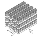
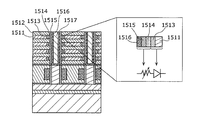
- FIG. 16 shows a memory cell array having a conventional stacked structure described in Patent Documents 1 and 2, an enlarged view of one memory cell, and an equivalent circuit diagram of the memory cell.
- This memory cell array includes a stacked body in which a plurality of conductive layers (N-type polysilicon) 1511 and a plurality of interlayer insulating films 1512 are alternately stacked, and a cylindrical resistor formed so as to intersect perpendicularly to the stacked body.
- a P-type polysilicon layer 1513 in contact with the N-type polysilicon layer 1511 and a metal silicide layer 1514 in contact with the P-type polysilicon layer 1513 are interposed between the change layer 1515 and the N-type polysilicon layer 1511.
- a stacked body of a metal layer 1516, a resistance change layer 1515, and a metal silicide layer 1514 functions as a resistance change element, and a P-type polysilicon layer 1513, an N-type polysilicon layer 1511, The stacked body functions as a PN diode.
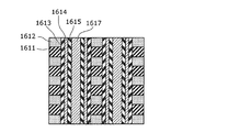
- FIG. 17 shows a memory cell array having a conventional stacked structure described in Patent Document 3.
- This memory cell array includes a stacked body in which a plurality of conductive layers 1611 and a plurality of interlayer insulating films 1612 are alternately stacked, a cylindrical resistance change layer 1613 formed so as to intersect perpendicularly to the stacked body, and a resistance
- a cylindrical first semiconductor layer 1614 formed in contact with the inner periphery of the change layer 1613, a cylindrical second semiconductor layer 1615 formed in contact with the inner periphery of the first semiconductor layer 1614, and a second semiconductor layer 1615. It is comprised by the columnar electrode 1616 formed in contact with the inner periphery.
- An object of the present invention is to solve the above-mentioned problems, to provide a nonvolatile memory cell, a nonvolatile memory cell array having a simple process and stable memory performance, and a manufacturing method thereof.
- a nonvolatile memory cell includes a columnar electrode arranged perpendicular to the main surface of the substrate and a parallel electrode to the main surface of the substrate.
- a variable resistance layer provided between the first conductive layer and having a resistance value reversibly changed based on application of an electrical signal; provided between the columnar electrode and the semiconductor layer;
- the semiconductor layer is disposed on the first conductive layer
- the second conductive layer is disposed on the semiconductor layer
- the resistance change layer includes the first conductive layer and the first conductive layer. It is good also as having the same base element.
- the variable resistance layer includes a first variable resistance layer having a first metal oxide and a second metal oxide having an oxygen deficiency greater than the oxygen deficiency of the first metal oxide.
- the second variable resistance layer may have a structure in which the second variable resistance layer is stacked in a direction parallel to the main surface of the substrate.
- the columnar electrode, the resistance change layer, and the first conductive layer constitute a resistance change element in a direction parallel to the main surface of the substrate, and the first conductive layer, the semiconductor layer, and the second conductive layer are A diode element having bidirectional rectification characteristics is formed in a direction perpendicular to the main surface of the substrate, and as a result, a nonvolatile memory cell in which the resistance change element and the diode element are connected in series is formed.
- a nonvolatile memory cell array includes a plurality of columnar electrodes arranged perpendicular to a substrate main surface, a first conductive layer arranged in parallel to the substrate main surface, A plurality of stacked bodies including a semiconductor layer disposed in contact with the first conductive layer in the stacking direction; a second conductive layer disposed in contact with the semiconductor layer in the stacking direction; and a plurality of interlayer insulating films.
- a non-volatile memory cell array manufacturing method in which an interlayer insulating film, a first conductive layer, a semiconductor layer, and a second conductive layer are stacked on a substrate in parallel with the main surface of the substrate.
- Step (b) and oxidizing the surface layer of the laminated structure exposed in the belt-like groove reversibly changes the resistance value based on an electrical signal applied to the surface layer of the first conductive layer.
- a non-volatile memory cell array manufacturing method in which an interlayer insulating film, a first conductive layer, a semiconductor layer, and a second conductive layer are stacked on a substrate in parallel with the main surface of the substrate. Forming a laminated structure and further forming at least one laminated structure equivalent to the laminated structure in parallel with the main surface of the substrate; and a plurality of layers penetrating the plurality of laminated structures in the lamination direction.
- the contact Forming a first resistance change layer having a resistance value reversibly changed on the inner wall of the contact hole based on an applied electric signal, and the contact
- the structure of the memory cell and the memory cell array according to the present invention can be manufactured by forming a resistance change layer by oxidizing a part of the conductive layer after forming the contact hole, the manufacturing process can be simplified.
- the uniformity of the film thickness can be easily controlled, and the reliability of the nonvolatile memory cell array is improved.
- it can be electrically separated by a series-connected diode so as to suppress crosstalk between adjacent memory cells.
- FIG. 1A is a cross-sectional view of the nonvolatile memory cell according to Embodiment 1 of the present invention.
- FIG. 1B is an equivalent circuit diagram of the nonvolatile memory cell according to Embodiment 1 of the present invention.
- FIG. 1C is a perspective view of the nonvolatile memory cell according to Embodiment 1 of the present invention.
- FIG. 1D is a perspective view of a nonvolatile memory cell according to a modification of Embodiment 1 of the present invention.
- FIG. 2A is a perspective view of the nonvolatile memory cell array according to Embodiment 2 of the present invention.
- FIG. 1A is a cross-sectional view of the nonvolatile memory cell according to Embodiment 1 of the present invention.
- FIG. 1B is an equivalent circuit diagram of the nonvolatile memory cell according to Embodiment 1 of the present invention.
- FIG. 1C is a perspective view of the nonvolatile memory cell according to Embodiment 1 of
- FIG. 2B is a cross-sectional view taken along the line A-A ′ of the nonvolatile memory cell array according to Embodiment 2 of the present invention.
- FIG. 2C is a B-B ′ cross-sectional view of the nonvolatile memory cell array according to Embodiment 2 of the present invention.
- FIG. 3 is an equivalent circuit diagram of the nonvolatile memory cell array according to Embodiment 2 of the present invention.
- FIG. 4 is a perspective view in the manufacturing process of the nonvolatile memory cell array according to Embodiment 2 of the present invention.
- FIG. 5 is a perspective view in the manufacturing process of the nonvolatile memory cell array according to Embodiment 2 of the present invention.
- FIG. 6 is a perspective view in the manufacturing process of the nonvolatile memory cell array according to Embodiment 2 of the present invention.
- FIG. 7 is an exploded perspective view of the main part in the manufacturing process of the nonvolatile memory cell array according to Embodiment 2 of the present invention.
- FIG. 8 is a graph showing the progress rate of oxidation of the material used for the nonvolatile memory cell array according to Embodiment 2 of the present invention.
- FIG. 9 is a perspective view in the manufacturing process of the nonvolatile memory cell array according to Embodiment 2 of the present invention.
- FIG. 10 is a perspective view in the manufacturing process of the nonvolatile memory cell array according to Embodiment 2 of the present invention.
- FIG. 10 is a perspective view in the manufacturing process of the nonvolatile memory cell array according to Embodiment 2 of the present invention.
- FIG. 11 is a perspective view in the manufacturing process of the nonvolatile memory cell array according to Embodiment 2 of the present invention.
- FIG. 12 is a perspective view in the manufacturing process of the nonvolatile memory cell array according to Embodiment 2 of the present invention.
- FIG. 13 is a perspective view in the manufacturing process of the nonvolatile memory cell array according to Embodiment 2 of the present invention.
- FIG. 14 is an exploded perspective view of the main part in the manufacturing process of the nonvolatile memory cell array according to Embodiment 2 of the present invention.
- FIG. 15A is a perspective view of a nonvolatile memory cell array according to a modification of Embodiment 2 of the present invention.
- FIG. 15A is a perspective view of a nonvolatile memory cell array according to a modification of Embodiment 2 of the present invention.
- FIG. 15B is a cross-sectional view taken along the line A-A ′ of the nonvolatile memory cell array according to the modification of the second embodiment of the present invention.
- FIG. 16 is a cross-sectional view of a conventional nonvolatile memory cell array, and an enlarged view and an equivalent circuit diagram of a memory cell.
- FIG. 17 is a cross-sectional view of a conventional nonvolatile memory cell.
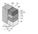
- FIG. 1A to 1C show a nonvolatile memory cell 10 according to Embodiment 1 of the present invention.
- 1A is a cross-sectional view of the nonvolatile memory cell 10
- FIG. 1B is an equivalent circuit diagram of the nonvolatile memory cell 10
- FIG. 1C is a perspective view of the nonvolatile memory cell 10.
- the nonvolatile memory cell 10 includes a columnar electrode 12, an interlayer insulating film 16, a resistance change layer 14, a first conductive layer 13, a semiconductor layer 17, and a second conductive layer 18. It is configured.
- a first resistance change layer 13a, a second resistance change layer 13b, and an insulating layer 13c are formed on a part of the first conductive layer 13.
- the resistance change layer 14 includes a first resistance change layer 13a and a second resistance change layer 13b.
- Insulating layers 17 a, 17 b, 18 a, and 18 b are formed on part of the semiconductor layer 17 and the second conductive layer 18.
- the interlayer insulating film 16 is formed in parallel with the main surface (not shown) of the substrate, the first conductive layer 13 is disposed in contact with the interlayer insulating film 16 in the stacking direction, and the first conductive layer 13 is stacked in the stacking direction.
- the semiconductor layer 17 is disposed in contact with the semiconductor layer 17, and the second conductive layer 18 is disposed in contact with the semiconductor layer 17 in the stacking direction.
- the first conductive layer 13, the semiconductor layer 17, and the second conductive layer 18 may be stacked in the order shown in FIGS. 1A and 1C, or may be stacked in the reverse order.
- the columnar electrode 12, the resistance change layer 14, and the first conductive layer 13 constitute a resistance change element 15 in a direction parallel to the main surface of the substrate.
- the first conductive layer 13, the semiconductor layer 17, and the second conductive layer 18 shows an MSM (Metal-Semiconductor-Metal) type diode element 19 having a bidirectional rectifying characteristic in a direction perpendicular to the main surface of the substrate, and the resistance change as shown in the equivalent circuit diagram of FIG. 1B
- a nonvolatile memory cell 10 is configured in which the element 15 and the diode element 19 are connected in series.
- the columnar electrode 12 and the second conductive layer 18 are drawn as wirings.
- the resistance change layer 14 is configured to be interposed between the columnar electrode 12 and the first conductive layer 13. Further, the resistance change layer 14 has a characteristic of changing to two or more states having different resistance values based on application of an electrical signal, and can be selectively changed from one state to another state. . Therefore, in the nonvolatile memory cell 10, the resistance value between the columnar electrode 12 and the first conductive layer 13 is selectively applied by applying a drive voltage or drive current between the columnar electrode 12 and the first conductive layer 13. Can be changed.
- the resistance change layer 14 has two states, a high resistance state with a relatively high electrical resistance value and a low resistance state with a low electrical resistance value.
- the nonvolatile memory cell 10 changes from a high resistance state to a low resistance state or from a low resistance state to a high resistance state by application of a driving voltage or driving current equal to or higher than a predetermined threshold.
- the resistance change layer 14 can be made of an oxygen-deficient metal oxide.
- the base metal of the metal oxide is preferably a transition metal such as tantalum (Ta), hafnium (Hf), titanium (Ti), tungsten (W), nickel (Ni), or iron (Fe).
- the oxygen-deficient metal oxide refers to a metal oxide having a lower oxygen content than the composition of a metal oxide having a stoichiometric composition (usually an insulator), and usually has a semiconducting behavior. There are many things to do.
- the oxygen-deficient oxide of the base metal exemplified above for the resistance change layer 14 the resistance change between the two resistance values can be stably operated with good reproducibility.
- the oxygen content of the resistance change layer 14 decreases from the interface between the resistance change layer 14 and the columnar electrode 12 toward the first conductive layer 13.
- the resistance change layer 14 can be formed so that the oxygen content of the resistance change layer 14 continuously decreases as the distance from the columnar electrode 12 increases. This is because in the oxidation process, the amount of oxygen that enters the first conductive layer 13 decreases as the distance from the contact hole increases.
- the layer having a relatively high oxygen content is the first resistance change layer 13a
- the layer having a relatively low oxygen content is the second resistance change layer 13b.
- the laminated structure is not clearly shown as shown in FIG. 1A. However, since it is important that the oxygen content in the region of the first resistance change layer 13a is larger than that of the second resistance change layer 13b, a laminated structure is illustrated for the sake of clarity.
- the oxidation treatment step is performed twice under different conditions, and the difference between the oxygen content of the first resistance change layer 13a and the oxygen content of the second resistance change layer 13b can be more clearly formed.
- the first resistance change layer 13a is applied with a positive drive voltage or drive current (current flows in the direction from the first resistance change layer 13a to the second resistance change layer 13b). It is presumed that oxygen ions are received from this and increase in resistance. On the contrary, it is presumed that, by applying a negative drive voltage or drive current, the first resistance change layer 13a diffuses the received oxygen ions into the second resistance change layer 13b, thereby reducing the resistance.
- the resistance change layer 14 is not limited to two layers. In order to develop a resistance change phenomenon in the single resistance change layer 14, a forming process (positive or negative voltage applied to the resistance change layer 14, a voltage higher than the voltage applied during normal operation is applied once to the resistance change layer 14. Alternatively, the step of electrically forming a layer having a large oxygen content in the vicinity of the interface to which a positive voltage is applied may be performed multiple times.
- the first conductive layer 13 may use an oxygen-deficient metal oxide having a low oxygen content (for example, a specific resistance of 10 m ⁇ ⁇ cm or less) or a metal not containing oxygen.
- a low oxygen content for example, a specific resistance of 10 m ⁇ ⁇ cm or less
- a metal not containing oxygen for example, a specific resistance of 10 m ⁇ ⁇ cm or less
- the variable resistance layer 14 can be easily formed from the first conductive layer 13.
- the resistance of the first conductive layer 13 is lowered, and there is an advantage that power consumption can be reduced.
- the semiconductor layer 17 is made of SiN y, for example.
- SiN y is so-called silicon nitride.
- the value of y indicates the degree of nitridation (composition ratio), and the electric conduction characteristics of SiN y vary greatly depending on the value of y.
- the semiconductor layer 17 may use amorphous Si or another semiconductor material.
- the first conductive layer 13 and the second conductive layer 18 are materials that contact the semiconductor layer 17 to form a Schottky junction, respectively.
- the first conductive layer 13, the semiconductor layer 17, and the second conductive layer 18 constitutes an MSM diode.
- the second conductive layer 18 may be made of TiN, TaN, or the like.
- an MSM diode composed of TaO x for the first conductive layer 13, SiN y for the semiconductor layer 17, and TaN for the second conductive layer 18 has bidirectional rectification characteristics with respect to the applied voltage, and breaks. While providing a current suppressing element with a large down current, a highly reliable nonvolatile memory element and nonvolatile memory device in which the diode element and the resistance change element are combined can be easily produced.
- the variable resistance layer 14 includes a first conductive layer 13, a semiconductor layer 17, and a second conductive layer 18 that are stacked in this order on the interlayer insulating film 16, and the first conductive layer 13, the semiconductor layer 17, and the second conductive layer are stacked.
- the contact hole is formed by forming a contact hole penetrating through the stacked body formed of the layer 18 and the interlayer insulating film 16 in the stacking direction, and then oxidizing part of the first conductive layer 13 exposed in the contact hole.
- the process of embedding the material in the contact hole is only the process of embedding the columnar electrode 12, and the process can be simplified. Further, by forming the resistance change layer 14 by oxidation treatment, there is an advantage that it is easy to control the film thickness of the resistance change layer 14.
- the first conductive layer 13 is oxidized, a part of the SiN y layer of the semiconductor layer 17 exposed in the contact hole is also oxidized, and an insulating layer 17a made of SiO 2 is formed on the surface, so that the semiconductor layer 17 and the columnar electrode 12 are insulated, and portions of TaN, TiN, etc. of the second conductive layer 18 exposed in the contact holes are simultaneously oxidized, and an insulating layer 18a composed of TaON, TiON, etc. is formed.
- the second conductive layer 18 and the columnar electrode 12 are insulated from each other.
- the columnar electrode 12 is a material having excellent conductivity (for example, a specific resistance of 10 m ⁇ ⁇ cm or less), and the standard electrode potential of the main metal material of the columnar electrode 12 is the standard electrode potential of the metal constituting the resistance change layer 14. What is necessary is just to comprise with a higher material.
- the material of the columnar electrode 12 with respect to the above-described variable resistance material platinum (Pt), iridium (Ir), palladium (Pd), copper (Cu), tungsten (W) (however, the variable resistance layer Is a tungsten oxide).
- the columnar electrode 12 may have a structure in which a thin film is formed of the above-exemplified material on the outer peripheral surface of a conductor made of tungsten (W) or the like.
- the reason why it is desirable that the standard electrode potential of the metal used for the columnar electrode 12 be higher than the standard electrode potential of the metal used for the first conductive layer 13 and the resistance change layer 14 is that the columnar electrode 12 is more than the resistance change layer 14. Since it becomes difficult to oxidize, the oxidation-reduction reaction of the resistance change layer 14 in the vicinity of the interface with the columnar electrode 12 mainly occurs, and the resistance change phenomenon is stabilized by changing the oxygen content of the first resistance change layer 13a. It is to do.
- the resistance change layer 14 is formed in one oxidation step, and at the same time, the semiconductor layer 17 and the second conductive layer 18 are electrically connected from the columnar electrode 12 respectively. Since the insulating film for separation is formed, the manufacturing process can be simplified. In addition, the uniformity of the thickness of the resistance change layer can be easily controlled, and the reliability of the nonvolatile memory cell array is improved.
- FIG. 1D is a configuration diagram showing an example of a nonvolatile memory cell 30 according to a modification of the first embodiment of the present invention.
- the nonvolatile memory cell 30 includes the resistance change element 15 included in the nonvolatile memory cell 10 of FIG. 1C by a first resistance change layer 31 and a second resistance change layer 32.
- the variable resistance layer 35 is replaced with a variable resistance element 35 using the variable resistance layer 34.
- the columnar electrode 12, the resistance change layer 34, and the first conductive layer 13 constitute a resistance change element 35 in a direction parallel to the main surface of the substrate, and the first conductive layer 13, the semiconductor layer 17.
- the second conductive layer 18 constitutes an MSM type diode element 19 having bidirectional rectification characteristics in a direction perpendicular to the main surface of the substrate.
- the nonvolatile memory cell 30 includes a variable resistance layer 34 provided between the columnar electrode 12 and the first conductive layer 13 and a variable resistance element 35 configured in a direction parallel to the main surface of the substrate.
- the device 19 has a feature common to the nonvolatile memory cell 10 in that the element 19 is formed in a direction perpendicular to the main surface of the substrate. Due to this common feature, the nonvolatile memory cell 30 and the nonvolatile memory cell 10 have the following advantages.
- the resistance values of the resistance change elements 15 and 35 change when the filaments (conductive paths) in the resistance change layers 14 and 34 change. Therefore, the higher the voltage or current density applied to the resistance change layers 14 and 34, the easier the resistance change occurs. Therefore, the area of the resistance change elements 15 and 35 is desirably small.
- the area refers to the area of a plane perpendicular to the voltage application direction.
- the diode element 19 preferably has a large current capacity in order to pass a large current (for example, 10000 A / cm 2 or more) through the resistance change elements 15 and 35. Since the size of the current capacity of the diode increases depending on the size of the junction area of the diode, the area of the diode element 19 is desirably large.
- the resistance change elements 15 and 35 are different in voltage application direction from the diode elements 19, so that the resistance change elements On the other hand, the area of the diode element 19 can be increased. Further, since the areas of the resistance change elements 15 and 35 are defined by the film thickness of the first conductive layer 13 that is horizontally laminated with respect to the main surface of the substrate, the areas of the resistance change elements 15 and 35 are reduced to, for example, the minimum processing It can also be below the dimension.
- the non-volatile memory cell 30 is formed such that the first resistance change layer 31 is in contact with and covers the side surface of the columnar electrode 12, and the second resistance change layer 32 is the first resistance change layer 32.
- the nonvolatile memory cell 10 is different from the nonvolatile memory cell 10 in that it is formed only at the intersection between the resistance change layer 31 and the first conductive layer 13.
- a contact hole for embedding the columnar electrode 12 is formed according to the same manufacturing process as the nonvolatile memory cell 10, and then the first resistance change layer 31 and the columnar electrode 12 are formed in the contact hole. It can be manufactured by embedding in this order.
- the step of embedding a material in the contact hole becomes two steps of embedding the first variable resistance layer 31 and the columnar electrode 12, and the step of forming the first variable resistance layer 31 and the second variable resistance layer 32 are formed.
- the process of performing can be made independent.
- the first resistance change layer 31 is replaced with the first resistance change layer 31 in place of the simplification of the manufacturing process and the ease of control of the film thickness of the resistance change layer 34 compared with the nonvolatile memory cell 10.
- the advantage that the freedom degree of material selection of the 2nd resistance change layer 32 increases is acquired.
- a combination of the first resistance change layer 31 and the second resistance change layer can be freely selected according to desired resistance change characteristics, oxidation characteristics, and the like.
- at least one material selected from high-resistance titanium oxide (for example, TiO 2 ), hafnium oxide (HfO y ), aluminum oxide (AlO y ), or the like is used for the first resistance change layer 31.
- Tantalum oxide (TaO x ) having a lower resistance value than that of the first resistance change layer 31 can be used for the second resistance change layer 32.
- the nonvolatile memory cell 30 for example, different transition metal oxides can be used for the first resistance change layer 31 and the second resistance change layer 32.
- the transition metal oxide of the first resistance change layer 31 a transition metal oxide having a smaller oxygen deficiency than the transition metal oxide of the second resistance change layer 32 is used.
- the degree of oxygen deficiency refers to the proportion of oxygen deficient with respect to the amount of oxygen constituting the stoichiometric oxide in each transition metal.
- the stoichiometric oxide composition is Ta 2 O 5 and can be expressed as TaO 2.5 .
- the degree of oxygen deficiency of TaO 2.5 is 0%.
- the oxygen content of Ta 2 O 5 is the ratio of oxygen to the total number of atoms (O / (Ta + O)), which is 71.4 atm%. Therefore, the oxygen-deficient tantalum oxide has an oxygen content greater than 0 and less than 71.4 atm%.
- the oxygen deficiency decreases as the oxygen content (oxygen content) increases, and the oxygen deficiency increases as the oxygen content (oxygen content) decreases.
- the oxygen deficiency is used instead of the oxygen content described above as a scale for uniformly comparing the degree of oxidation deficiency of the transition metal oxide regardless of the type of the base metal.
- the first conductive layer 13 and the columnar electrode 12 at the time of resistance change.
- the voltage applied therebetween is more distributed to the first variable resistance layer 31 of the variable resistance layer 34, and the oxidation-reduction reaction that occurs in the first variable resistance layer 31 of the variable resistance layer 34 is more likely to occur. Can do.
- the standard electrode potential of the transition metal of the first resistance change layer 31 is the second It is preferable that the resistance change layer 32 be lower than the standard electrode potential of the transition metal.
- the resistance change phenomenon occurs when an oxidation-reduction reaction occurs in a minute filament (conductive path) formed in the transition metal oxide layer of the first resistance change layer 31 having a high resistance, and the resistance value changes. It is possible.
- an oxygen-deficient tantalum oxide formed by oxidation of the first conductive layer 13 is used as the transition metal oxide of the second resistance change layer 32, and the transition metal oxide of the first resistance change layer 31 is used.
- the standard electrode potential represents a characteristic that the higher the value, the less likely it is to oxidize.
- the columnar electrode 12 of the nonvolatile memory cell 30 is preferably made of a material whose standard electrode potential of the main metal material is higher than the standard electrode potential of the metal constituting the first resistance change layer 31.
- This is based on the same idea as the nonvolatile memory cell 10. That is, since such a columnar electrode 12 is less likely to be oxidized than the first variable resistance layer 31, the oxidation-reduction reaction of the first variable resistance layer 31 mainly occurs in the vicinity of the interface with the columnar electrode 12. This is because the resistance change phenomenon is stabilized by changing the oxygen content of the resistance change layer 31.
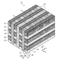
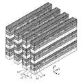
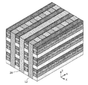
- FIG. 2A is a perspective view of the nonvolatile memory cell array 20.
- 2B and 2C are cross-sectional views taken along lines AA ′ and BB ′ shown in the perspective views of the nonvolatile memory cell array 20, respectively.
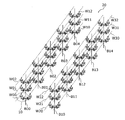
- FIG. 3 is an equivalent circuit diagram of the nonvolatile memory cell array 20. Below, it demonstrates according to the direction of XYZ shown by the arrow in the figure.
- the nonvolatile memory cell array 20 includes three interlayer insulating films 16 and three stacked bodies 21 arranged alternately in the Z direction (direction perpendicular to the substrate). Each memory cell array includes 20 memory cells (4 in the X direction ⁇ 5 in the Y direction), and a total of 60 memory cells are arranged in a three-dimensional manner.
- the nonvolatile memory cell array 20 is configured on a substrate (not shown) having a main surface parallel to the XY plane.
- each of the memory cells corresponds to the nonvolatile memory cell 10 in the first embodiment, and the columnar electrode 12, the interlayer insulating film 16, the first conductive layer 13, the first resistance change layer 13a, and the second
- the variable resistance layer 14 includes a variable resistance layer 13 b, a semiconductor layer 17, and a second conductive layer 18.
- Nonvolatile memory cell 10 is represented in the cross section of FIG. 2B.
- the columnar electrode 12 does not exist, and the first conductive layer 13 is oxidized over the entire width in the X direction to form an insulating layer 13c. Therefore, the cross-sectional structure shown in FIG. 2C functions as element isolation for isolating the nonvolatile memory cells 10 adjacent in the Y direction.
- the process is simplified as in the first embodiment.
- the resistance change layer 14 is formed only at the intersection of the columnar electrode 12 and the first conductive layer 13, a memory cell array in which the resistance change layer 14 is separated for each memory cell can be realized.
- the thickness of the resistance change layer 14 formed by the oxidation process can be controlled uniformly over the plurality of resistance change layers 14 in the contact hole, compared to the resistance change layer formed by burying. Therefore, the reliability of the nonvolatile memory cell array 20 having a stacked structure is improved.
- the stacked body 21 composed of the interlayer insulating film 16, the first conductive layer 13, the semiconductor layer 17, and the second conductive layer 18 is alternately stacked in parallel to the main surface of the substrate.
- the columnar electrodes 12 are arranged in a columnar shape perpendicular to the main surface of the substrate and distributed in a matrix on the substrate main surface (that is, distributed in an array in the X and Y directions). Functions as a bit line.
- the second conductive layer 18 functions as a word line.
- planar insulating layer 26 arranged in the YZ plane at the center of FIG. 2A allows two memory cells 10 arranged in four rows in the row (X) direction at the center of the nonvolatile memory cell array 20. It is formed so as to divide into one by one. That is, in FIG. 2A, the columnar electrodes 12 of the memory cell 10 located on both sides of the insulating layer 26 disposed on the central YZ plane are separated from each other by the insulating layer 26.
- non-volatile memory cell array 20 such a configuration is repeatedly provided in the X direction, thereby reducing a sneak current through the non-selected bit line, the non-selected word line, and the non-selected memory cell. Can be made.
- FIG. 3 is an equivalent circuit diagram of the nonvolatile memory cell array 20 according to the second embodiment. 3, columnar electrodes 12 (bit lines: B00, B01,..., B11,...) And second conductive layers 18 (word lines: W00, W01,..., W30, W31,...
- the non-volatile memory cell 10 is arranged at the intersection of (). That is, by selecting one bit line (for example, B00) and one word line (for example, W00) and applying a drive voltage to the nonvolatile memory cell 10 located at the intersection, the resistance value of the nonvolatile memory cell 10 The state of can be changed.
- the drive voltage is applied to the bit line and the word line connected to the nonvolatile memory cell 10, thereby Information can be written or information can be read from the nonvolatile memory cell 10.
- the nonvolatile memory cell array 20 having random accessibility can be realized.
- the memory cell array composed of the bit lines B00 to B04 and the word lines W00 to W12 and the memory cell array composed of the bit lines B10 to B14 and the word lines W20 to W32 are completely at the wiring level. Therefore, the sneak current can be reduced.
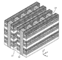
- the laminated body 21 including the interlayer insulating film 16, the first conductive layer 13, the semiconductor layer 17, and the second conductive layer 18 is formed.
- the stacked structure shown in FIG. 4 includes three stacked bodies 21, the number of stacked bodies 21 in the stacked structure is not particularly limited to this number.
- tantalum (Ta) or oxygen-deficient tantalum oxide TaO x (specific resistance is 10 m ⁇ ⁇ cm or less) is deposited as the first conductive layer 13 by sputtering, and is nitrided by sputtering. Silicon SiN y is deposited as the semiconductor layer 17. Further, tantalum nitride (TaN) is deposited as the second conductive layer 18 by sputtering. In each sputtering method, a reactive sputtering method in which oxygen or nitrogen is introduced during sputtering may be used.
- an interlayer insulating film 16 may be further formed on the uppermost second conductive layer 18.
- a belt-like groove 27 is formed in the YZ direction perpendicular to the main surface of the laminated structure.
- a mask pattern having a predetermined pattern shape is formed by a normal exposure process and development process.
- the laminated structure is etched to form a strip-like groove 27.
- the mask pattern is removed.
- the side surfaces of the interlayer insulating film 16, the first conductive layer 13, the semiconductor layer 17, and the second conductive layer 18 are oxidized from the surface exposed in the belt-like groove 27.
- the resistance change layer 14 is formed by oxidizing the side surface of the first conductive layer 13.
- plasma oxidation is performed in an oxygen atmosphere with an applied power of 1100 W and a processing time of 30 seconds.
- Active oxygen, oxygen ions, or oxygen atoms diffuse from the surface of the first conductive layer 13 exposed in the band-shaped groove 27 toward the inside of the first conductive layer 13.
- an oxide having a predetermined oxygen deficiency profile is formed in the first conductive layer 13 in a region having a certain thickness from the surface exposed in the band-shaped groove 27 to the inside. .
- This oxygen deficiency profile is high near the surface and continuously decreases toward the inside.
- the resistance change layer 14 is formed over a depth of about 10 nm from the surface exposed in the belt-like groove 27.
- the first resistance change layer 13a having a smaller oxygen deficiency is formed in a region of about 2 to 3 nm from the surface, and the oxygen deficiency in a region of about 7 to 8 nm from the first resistance change layer 13a.
- the second resistance change layer 13b having a larger value is formed.
- thermal oxidation treatment heat treatment in an atmosphere containing oxygen
- plasma oxidation treatment plasma oxidation treatment
- oxidation treatment heat treatment in an atmosphere containing oxygen
- thermal oxidation treatment and plasma oxidation treatment are collectively referred to as oxidation treatment.
- the resistance change layer 14 is formed by oxidizing part of the first conductive layer 13
- the process can be simplified as compared with a conventional conductive layer embedding step.
- the film thickness can be easily controlled as compared with the embedding process, and the film thickness is uniformly formed over the plurality of resistance change layers 14 exposed in the belt-like groove 27.
- the oxidation treatment process is not limited to one time.
- the oxidation treatment process is performed twice, and the difference between the oxygen deficiency of the first resistance change layer 13a and the oxygen deficiency of the second resistance change layer 13b can be more clearly formed.
- the oxidation treatment step may be performed two or more times to control the oxygen deficiency of the resistance change layer 14 with higher accuracy.
- the side walls of the semiconductor layer 17 and the second conductive layer 18 are also oxidized, and insulating layers 17 a, 17 b, 18 a, 18 b are formed on the surfaces exposed in the band-shaped grooves 27. .
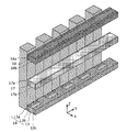
- FIG. 7 is an exploded perspective view showing an example of the shapes of the first conductive layer 13, the semiconductor layer 17, and the second conductive layer 18 after the plasma oxidation process under the above-described conditions.
- TaO x which is the first conductive layer 13 is oxidized about 10 nm from the surface.
- the oxidized portions of the first conductive layer 13 become the first resistance change layer 13a and the second resistance change layer 13b.
- SiN y which is the semiconductor layer 17 is oxidized about 2 to 3 nm from the surface to become SiO 2 containing nitrogen which is an insulator. Oxidized portions of the semiconductor layer 17 become insulating layers 17a and 17b.
- the TaN which is the second conductive layer 18 is oxidized about 5 nm from the surface to become TaON which is an insulator. Oxidized portions of the second conductive layer 18 become insulating layers 18a and 18b.
- the first conductive layer 13, the semiconductor layer 17, and the second conductive layer 18 are oxidized at portions having different sizes even if the same oxidation treatment is performed due to the difference in materials.
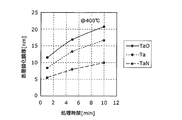
- FIG. 8 is a graph showing the rate of progress of oxidation in each material of TaO, Ta, and TaN. The time during which the oxidation treatment was performed on each material in an oxygen atmosphere at 400 ° C., and the results of the oxidation treatment for each material. The thickness of the oxide film formed on the surface layer (the rate of progress of oxidation) is shown. This graph is based on the results of experiments conducted preliminary to find suitable conditions for the oxidation treatment.
- the oxidation of TaO x which is the material of the first conductive layer 13 progresses at a rate more than double that of TaN which is the material of the second conductive layer 18. This is consistent with the example shape seen in FIG.
- the difference in the rate of progress of oxidation between the first conductive layer 13 and the second conductive layer 18 is also important in the oxidation step for providing element isolation described later.
- polysilicon 28 is deposited by CVD in the previously formed belt-like groove 27. Thereafter, unnecessary polysilicon is removed by polishing, leaving the polysilicon 28 formed in the belt-like groove 27 by CMP process or other planarization process.
- a part of the polysilicon 28 is removed in a direction perpendicular to the main surface of the substrate and in an array form on the main surface of the substrate to form a contact hole 29.
- a photoresist mask pattern having a predetermined pattern shape is formed by a normal photolithography process.
- the stacked structure is etched to form contact holes 29.
- the mask pattern is removed.
- a hard mask may be used.
- the columnar electrode 12 is deposited in the contact hole 29 by sputtering, CVD, plating or the like.
- a material of the columnar electrode 12 for example, a conductive material such as platinum (Pt), iridium (Ir), palladium (Pd), copper (Cu), tungsten (W) is used.
- unnecessary electrode material is removed by polishing, leaving the columnar electrode 12 formed inside the contact hole 29 by CMP (Chemical Mechanical Polishing) process or other planarization process.
- the columnar electrode 12 is in direct contact with the first variable resistance layer 13a, is in contact with the semiconductor layer 17 through the insulating layer 17a, and is in contact with the second conductive layer 18 through the insulating layer 18a. Yes.
- the polysilicon 28 in the region other than the columnar electrode 12 in the belt-like groove 27 is removed by wet etching using an HF: HNO 3 solution.
- the interlayer insulating film 16 exposed in a space formed by removing the polysilicon 28 in the strip groove 27 (for convenience, this space is also referred to as the strip groove 27).
- the first conductive layer 13, the semiconductor layer 17, and the second conductive layer 18 are oxidized.
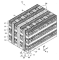
- FIG. 14 is an exploded perspective view showing an example of the shapes of the first conductive layer 13, the semiconductor layer 17, and the second conductive layer 18 after the oxidation treatment.
- the regions of the first conductive layer 13, the semiconductor layer 17, and the second conductive layer 18 that are in contact with the columnar electrode 12 are protected by the columnar electrode 12, so that the oxidation does not proceed. Therefore, the resistance change layer 14 and the insulating layers 17a and 18a adjacent to the columnar electrode 12 are maintained in the shape shown in FIG.
- the region exposed in the strip-shaped groove 27 of the first conductive layer 13 is completely oxidized (Ta 2 O 5 ) up to about half of the width of the first conductive layer 13 in the X direction, and the insulating layer 13c. become.
- oxidation proceeds from both sides, so that the entire section becomes the insulating layer 13c.
- This section is element isolation that separates adjacent resistance change layers 14.
- the region exposed in the band-like groove 27 of the semiconductor layer 17 has the insulating layers 17a and 17b as the SiO 2 protective film on the surface, so that the oxidation does not proceed to the inside.
- the thickness of TaON is thick, but as shown in the graph of FIG. Since the oxidation rate is slower than that of the region, a TaN region which is the second conductive layer 18 remains inside and can function as a word line.
- the nonvolatile memory cell array 20 shown in FIG. 2A is formed by embedding SiO 2 as the insulating layer 26 in the space formed by removing the polysilicon 28 in the belt-like groove 27. Complete.
- the filling material is at least temporarily embedded in the belt-shaped groove, and is a laminate 21 composed of the interlayer insulating film 16, the first conductive layer 13, the semiconductor layer 17, and the second conductive layer 18 in a later step. Any material that can be selectively removed by wet etching or the like may be used.
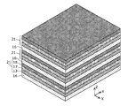
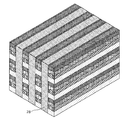
- FIG. 15A is a perspective view showing an example of a nonvolatile memory cell array 40 according to a modification of the second embodiment of the present invention.
- FIG. 15B is a cross-sectional view taken along line A-A ′ shown in the perspective view of the nonvolatile memory cell array 40.
- the cross-sectional view taken along the line B-B ′ of the nonvolatile memory cell array 40 is the same as the cross-sectional view taken along the line B-B ′ of the nonvolatile memory cell array 20 shown in FIG.
- the nonvolatile memory cell array 40 includes a nonvolatile memory cell 10 included in the nonvolatile memory cell array 20 of FIGS. 2A and 2B, and the nonvolatile memory cell array 40 according to the modification of the first embodiment.
- the memory cell 30 is replaced.
- the nonvolatile memory cell array 40 is different from the nonvolatile memory cell array 20 in that the first resistance change layer 31 is formed so as to be in contact with and cover the side surface of the columnar electrode 12. 15A and 15B, in the nonvolatile memory cell array 40, the first resistance change layer 31 includes not only the intersection between the columnar electrode 12 and the second resistance change layer 32, but also the columnar electrode 12
- the semiconductor layer 17 is continuously provided at the intersection, the intersection between the columnar electrode 12 and the second conductive layer 18, and the intersection between the columnar electrode 12 and the interlayer insulating film 16.
- Such a shape is formed by embedding the first variable resistance layer 31 and the columnar electrode 12 in this order in the contact hole as described in the modification of the first embodiment.
- the first wall is formed on the inner wall of the contact hole 29 by sputtering, CVD, plating, or the like.
- the material of the resistance change layer 31 is deposited in a thin film shape.
- a material of the first variable resistance layer 31 for example, transition using tantalum (Ta), hafnium (Hf), titanium (Ti), tungsten (W), nickel (Ni), iron (Fe), or the like as a base metal.
- a metal oxide can be used, and in particular, a transition metal oxide having a base metal different from that of the second resistance change layer 32 can be used.
- the step of embedding a material in the contact hole includes two steps of embedding the first resistance change layer 31 and the columnar electrode 12, and the step of forming the first resistance change layer 31 and the first step.
- the step of forming the second resistance change layer 32 can be made independent.
- the first resistance change layer 31 is replaced with the first resistance change layer 31 in place of simplifying the manufacturing process and controlling the film thickness of the resistance change layer 34 slightly inferior to the nonvolatile memory cell array 20.
- the advantage that the degree of freedom of material selection increases.
- the manufacturing method of the present invention is not limited to the nonvolatile memory cell array exemplified in Embodiment 2, and can be applied. That is, it is possible to manufacture an electronic device including a variable resistance element in general by the above manufacturing method or by combining the above manufacturing method and a known method.
- the nonvolatile memory cell array according to the present invention is useful as a next-generation nonvolatile memory or the like aimed at low power, high-speed writing, high-speed erasing, and large capacity.
- Nonvolatile memory cell 12 Columnar electrode 13 1st conductive layer 13a, 31 1st resistance change layer 13b, 32 2nd resistance change layer 13c Insulation layer 14, 34 Resistance change layer 15, 35 Resistance change element 16 Interlayer insulating film 17 Semiconductor layer 17a, 17b Insulating layer 18 Second conductive layer 18a, 18b Insulating layer 19 Diode element 20, 40 Non-volatile memory cell array 21 Stack 26 Insulating layer 27 Strip groove 28 Polysilicon 29 Contact hole 1511 N-type Polysilicon layer 1512 Interlayer insulation film 1513 P-type polysilicon layer 1514 Metal silicide layer 1515 Resistance change layer 1516 Metal layer 1517 Columnar electrode 1611 Conductive layer 1612 Interlayer insulation film 1613 Resistance change layer 1614 First semiconductor layer 1615 Second semiconductor layer 616 columnar electrodes
Abstract
Description
前記帯状溝内の前記ポリシリコンの残部が除去されてできた空間に露出した前記第1の導電層を酸化することにより絶縁膜を形成する工程(g)と、を含む。
図1A~図1Cに本発明の実施の形態1に係る不揮発性メモリセル10を示す。図1Aは不揮発性メモリセル10の断面図であり、図1Bは不揮発性メモリセル10の等価回路図であり、図1Cは不揮発性メモリセル10の斜視図である。
次に、本発明の実施の形態1の変形例に係る不揮発性メモリセルについて説明する。
図2A~図2C、図3に本発明の実施の形態2に係る不揮発性メモリセルアレイ20の一例を示す。図2Aは不揮発性メモリセルアレイ20の斜視図である。図2B、図2Cはそれぞれ不揮発性メモリセルアレイ20の斜視図に示されたA-A’線、B-B’線における断面図である。図3は不揮発性メモリセルアレイ20の等価回路図である。以下では、図中に矢印で示したXYZの方向に従って説明する。
次に、本発明の実施の形態2の変形例に係る不揮発性メモリセルアレイについて説明する。
12 柱状電極
13 第1の導電層
13a、31 第1の抵抗変化層
13b、32 第2の抵抗変化層
13c 絶縁層
14、34 抵抗変化層
15、35 抵抗変化素子
16 層間絶縁膜
17 半導体層
17a、17b 絶縁層
18 第2の導電層
18a、18b 絶縁層
19 ダイオード素子
20、40 不揮発性メモリセルアレイ
21 積層体
26 絶縁層
27 帯状溝
28 ポリシリコン
29 コンタクトホール
1511 N型ポリシリコン層
1512 層間絶縁膜
1513 P型ポリシリコン層
1514 金属シリサイド層
1515 抵抗変化層
1516 金属層
1517 柱状電極
1611 導電層
1612 層間絶縁膜
1613 抵抗変化層
1614 第1半導体層
1615 第2半導体層
1616 柱状電極
Claims (20)
- 基板主面に対して垂直に配置された柱状電極と、
前記基板主面に対して平行に配置された第1の導電層と、
前記第1の導電層に積層方向に接して配置された半導体層と、
前記半導体層に積層方向に接して配置された第2の導電層と、
前記柱状電極と前記第1の導電層との間に設けられ、かつ電気的信号の印加に基づいて可逆的に抵抗値が変化する抵抗変化層と、
前記柱状電極と前記半導体層との間に設けられ、前記半導体層と同じ母体元素を有する酸化物絶縁層と、
前記柱状電極と前記第2の導電層との間に設けられた絶縁層と、を備える、
不揮発性メモリセル。 - 前記半導体層は、前記第1の導電層の上に配置され、
前記第2の導電層は、前記半導体層の上に配置され、
前記抵抗変化層は、前記第1の導電層と同じ母体元素を有している、
請求項1に記載の不揮発性メモリセル。 - 前記抵抗変化層は、前記柱状電極と前記第1の導電層との交差部にのみ形成されている、
請求項2に記載の不揮発性メモリセル。 - 前記抵抗変化層は、前記抵抗変化層と前記柱状電極との界面から前記第1の導電層へ向かって、前記抵抗変化層の酸素不足度が大きくなる、
請求項2に記載の不揮発性メモリセル。 - 前記第2の導電層は、前記抵抗変化層と同じ母体金属で構成される、
請求項1に記載の不揮発性メモリセル。 - 前記抵抗変化層は、第1の金属酸化物を有する第1の抵抗変化層と、酸素不足度が前記第1の金属酸化物の酸素不足度よりも大きい第2の金属酸化物を有する第2の抵抗変化層とが前記基板主面に対して平行な方向に積層された構造である、
請求項1に記載の不揮発性メモリセル。 - 前記第1の抵抗変化層は、前記柱状電極の側面に接して、当該側面を被覆するように形成され、
前記第2の抵抗変化層は、前記第1の抵抗変化層と前記第1の導電層との交差部のみに形成されている、
請求項6に記載の不揮発性メモリセル。 - 基板主面に対し垂直に配置された複数の柱状電極と、
前記基板主面に対して平行に配置された第1の導電層と、前記第1の導電層に積層方向に接して配置された半導体層と、前記半導体層に積層方向に接して配置された第2の導電層とからなる複数の積層体と、複数の層間絶縁膜とが、交互に積層された積層構造と、
前記柱状電極と前記各第1の導電層との間に設けられ、かつ電気的信号の印加に基づいて可逆的に抵抗値が変化する抵抗変化層と、
前記柱状電極と前記各半導体層との間に設けられ、前記半導体層と同じ母体元素を有する酸化物絶縁層と、
前記柱状電極と前記各第2の導電層との間に設けられた絶縁層と、を備える、
不揮発性メモリセルアレイ。 - 前記半導体層は、前記第1の導電層の上に配置され、
前記第2の導電層は、前記半導体層の上に配置され、
前記抵抗変化層は、前記第1の導電層と同じ母体元素を有している、
請求項8に記載の不揮発性メモリセルアレイ。 - 前記抵抗変化層は、前記柱状電極と前記第1の導電層との交差部にのみ形成されている、
請求項9に記載の不揮発性メモリセルアレイ。 - 前記抵抗変化層は、前記抵抗変化層と前記柱状電極との界面から前記第1の導電層へ向かって、前記抵抗変化層の酸素不足度が大きくなる、
請求項9に記載の不揮発性メモリセルアレイ。 - 前記第2の導電層は、前記抵抗変化層と同じ母体金属で構成される、
請求項8に記載の不揮発性メモリセルアレイ。 - 前記抵抗変化層は、第1の金属酸化物を有する第1の抵抗変化層と、酸素不足度が前記第1の金属酸化物の酸素不足度よりも大きい第2の金属酸化物を有する第2の抵抗変化層とが前記基板主面に対して平行な方向に積層された構造である、
請求項8に記載の不揮発性メモリセルアレイ。 - 前記第1の抵抗変化層は、前記柱状電極の側面に接して、当該側面を被覆するように形成され、
前記第2の抵抗変化層は、前記第1の抵抗変化層と前記第1の導電層との交差部のみに形成されている、
請求項13に記載の不揮発性メモリセルアレイ。 - 前記複数の柱状電極は、前記基板主面内に行列状に分布する位置に配置される、
請求項8に記載の不揮発性メモリセルアレイ。 - 前記抵抗変化層は、酸素不足型金属酸化物で構成される、
請求項8に記載の不揮発性メモリセルアレイ。 - 前記第1の導電層および前記抵抗変化層の母体金属元素はタンタルである、
請求項8に記載の不揮発性メモリセルアレイ。 - 基板上に、層間絶縁膜、第1の導電層、半導体層、及び第2の導電層を前記基板の主面に平行に積層して積層構造を形成し、さらに前記積層構造と同等の積層構造を前記基板の主面に平行に1つ以上形成する工程(a)と、
前記複数の積層構造を積層方向に貫通する複数の帯状溝を形成する工程(b)と、
前記複数の帯状溝の側面に露出する前記積層構造の側面表層を酸化させることにより、前記第1の導電層の側面表層に、与えられる電気的信号に基づいて可逆的に抵抗値が変化する抵抗変化層を形成すると同時に、前記半導体層、前記第2の導電層の側面表層にそれぞれ絶縁膜を形成する工程(c)と、
前記帯状溝に充填材料を埋め込み、前記充填材料の一部をエッチングにて除去することにより、コンタクトホールを形成する工程(d)と、
前記コンタクトホールに導電性材料を埋め込むことにより、前記コンタクトホール中に前記抵抗変化層に接続する柱状電極を形成する工程(e)と、
前記帯状溝内の前記充填材料の残部を除去する工程(f)と、
前記帯状溝内の前記充填材料の残部が除去されてできた空間に露出した前記第1の導電層を酸化することにより絶縁膜を形成する工程(g)と、を含む、
不揮発性メモリセルアレイの製造方法。 - 前記工程(c)において、酸化処理を2回行い、酸素含有量が大きい第1の抵抗変化層と、酸素含有量が小さい第2の抵抗変化層をそれぞれ形成する、
請求項18に記載の不揮発性メモリセルアレイの製造方法。 - 基板上に、層間絶縁膜、第1の導電層、半導体層、及び第2の導電層を前記基板の主面に平行に積層して積層構造を形成し、さらに前記積層構造と同等の積層構造を前記基板の主面に平行に1つ以上形成する工程(a)と、
前記複数の積層構造を積層方向に貫通する複数の帯状溝を形成する工程(b)と、
前記複数の帯状溝の側面に露出する前記積層構造の側面表層を酸化させることにより、前記第1の導電層の側面表層に、第2の抵抗変化層を形成すると同時に、前記半導体層、前記第2の導電層の側面表層にそれぞれ絶縁膜を形成する工程(h)と、
前記帯状溝に充填材料を埋め込み、前記充填材料の一部をエッチングにて除去することにより、コンタクトホールを形成する工程(d)と、
前記コンタクトホールの内壁に、与えられる電気的信号に基づいて可逆的に抵抗値が変化する第1の抵抗変化層を形成する工程(i)と、
前記コンタクトホールに導電性材料を埋め込むことにより、前記コンタクトホール中に前記第1の抵抗変化層に接続する柱状電極を形成する工程(j)と、
前記帯状溝内の前記充填材料の残部を除去する工程(f)と、
前記帯状溝内の前記充填材料の残部が除去されてできた空間に露出した前記第1の導電層を酸化することにより絶縁膜を形成する工程(g)と、を含む、
不揮発性メモリセルアレイの製造方法。
Priority Applications (3)
| Application Number | Priority Date | Filing Date | Title |
|---|---|---|---|
| CN2011800026542A CN102473707A (zh) | 2010-07-01 | 2011-06-29 | 非易失性存储单元、非易失性存储单元阵列、以及其制造方法 |
| JP2011544316A JP4921620B2 (ja) | 2010-07-01 | 2011-06-29 | 不揮発性メモリセル、不揮発性メモリセルアレイ、およびその製造方法 |
| US13/382,321 US9006793B2 (en) | 2010-07-01 | 2011-06-29 | Non-volatile memory cell, non-volatile memory cell array, and method of manufacturing the same |
Applications Claiming Priority (2)
| Application Number | Priority Date | Filing Date | Title |
|---|---|---|---|
| JP2010151400 | 2010-07-01 | ||
| JP2010-151400 | 2010-07-01 |
Publications (1)
| Publication Number | Publication Date |
|---|---|
| WO2012001960A1 true WO2012001960A1 (ja) | 2012-01-05 |
Family
ID=45401700
Family Applications (1)
| Application Number | Title | Priority Date | Filing Date |
|---|---|---|---|
| PCT/JP2011/003697 WO2012001960A1 (ja) | 2010-07-01 | 2011-06-29 | 不揮発性メモリセル、不揮発性メモリセルアレイ、およびその製造方法 |
Country Status (4)
| Country | Link |
|---|---|
| US (1) | US9006793B2 (ja) |
| JP (1) | JP4921620B2 (ja) |
| CN (1) | CN102473707A (ja) |
| WO (1) | WO2012001960A1 (ja) |
Cited By (4)
| Publication number | Priority date | Publication date | Assignee | Title |
|---|---|---|---|---|
| WO2014103577A1 (ja) * | 2012-12-26 | 2014-07-03 | ソニー株式会社 | 記憶装置およびその製造方法 |
| US9704922B2 (en) | 2015-05-29 | 2017-07-11 | Kabushiki Kaisha Toshiba | Semiconductor memory device and method of manufacturing the same while avoiding process damage to a variable resistance film |
| US9721961B2 (en) | 2015-05-29 | 2017-08-01 | Kabushiki Kaisha Toshiba | Semiconductor memory device |
| WO2018190071A1 (ja) * | 2017-04-11 | 2018-10-18 | ソニーセミコンダクタソリューションズ株式会社 | 記憶装置 |
Families Citing this family (69)
| Publication number | Priority date | Publication date | Assignee | Title |
|---|---|---|---|---|
| US9012307B2 (en) | 2010-07-13 | 2015-04-21 | Crossbar, Inc. | Two terminal resistive switching device structure and method of fabricating |
| US9601692B1 (en) | 2010-07-13 | 2017-03-21 | Crossbar, Inc. | Hetero-switching layer in a RRAM device and method |
| US9570678B1 (en) | 2010-06-08 | 2017-02-14 | Crossbar, Inc. | Resistive RAM with preferental filament formation region and methods |
| US8946046B1 (en) | 2012-05-02 | 2015-02-03 | Crossbar, Inc. | Guided path for forming a conductive filament in RRAM |
| US8198144B2 (en) | 2010-06-11 | 2012-06-12 | Crossbar, Inc. | Pillar structure for memory device and method |
| US8441835B2 (en) | 2010-06-11 | 2013-05-14 | Crossbar, Inc. | Interface control for improved switching in RRAM |
| US8374018B2 (en) | 2010-07-09 | 2013-02-12 | Crossbar, Inc. | Resistive memory using SiGe material |
| US8467227B1 (en) | 2010-11-04 | 2013-06-18 | Crossbar, Inc. | Hetero resistive switching material layer in RRAM device and method |
| US8947908B2 (en) | 2010-11-04 | 2015-02-03 | Crossbar, Inc. | Hetero-switching layer in a RRAM device and method |
| US8168506B2 (en) | 2010-07-13 | 2012-05-01 | Crossbar, Inc. | On/off ratio for non-volatile memory device and method |
| US8569172B1 (en) | 2012-08-14 | 2013-10-29 | Crossbar, Inc. | Noble metal/non-noble metal electrode for RRAM applications |
| US8884261B2 (en) | 2010-08-23 | 2014-11-11 | Crossbar, Inc. | Device switching using layered device structure |
| US9401475B1 (en) | 2010-08-23 | 2016-07-26 | Crossbar, Inc. | Method for silver deposition for a non-volatile memory device |
| US8492195B2 (en) | 2010-08-23 | 2013-07-23 | Crossbar, Inc. | Method for forming stackable non-volatile resistive switching memory devices |
| US8404553B2 (en) * | 2010-08-23 | 2013-03-26 | Crossbar, Inc. | Disturb-resistant non-volatile memory device and method |
| US8889521B1 (en) | 2012-09-14 | 2014-11-18 | Crossbar, Inc. | Method for silver deposition for a non-volatile memory device |
| US8391049B2 (en) | 2010-09-29 | 2013-03-05 | Crossbar, Inc. | Resistor structure for a non-volatile memory device and method |
| US8558212B2 (en) | 2010-09-29 | 2013-10-15 | Crossbar, Inc. | Conductive path in switching material in a resistive random access memory device and control |
| USRE46335E1 (en) | 2010-11-04 | 2017-03-07 | Crossbar, Inc. | Switching device having a non-linear element |
| US8502185B2 (en) | 2011-05-31 | 2013-08-06 | Crossbar, Inc. | Switching device having a non-linear element |
| US8088688B1 (en) | 2010-11-05 | 2012-01-03 | Crossbar, Inc. | p+ polysilicon material on aluminum for non-volatile memory device and method |
| US8930174B2 (en) | 2010-12-28 | 2015-01-06 | Crossbar, Inc. | Modeling technique for resistive random access memory (RRAM) cells |
| US9153623B1 (en) | 2010-12-31 | 2015-10-06 | Crossbar, Inc. | Thin film transistor steering element for a non-volatile memory device |
| US8815696B1 (en) | 2010-12-31 | 2014-08-26 | Crossbar, Inc. | Disturb-resistant non-volatile memory device using via-fill and etchback technique |
| US8791010B1 (en) | 2010-12-31 | 2014-07-29 | Crossbar, Inc. | Silver interconnects for stacked non-volatile memory device and method |
| US8450710B2 (en) | 2011-05-27 | 2013-05-28 | Crossbar, Inc. | Low temperature p+ silicon junction material for a non-volatile memory device |
| US8394670B2 (en) | 2011-05-31 | 2013-03-12 | Crossbar, Inc. | Vertical diodes for non-volatile memory device |
| US9620206B2 (en) | 2011-05-31 | 2017-04-11 | Crossbar, Inc. | Memory array architecture with two-terminal memory cells |
| US8619459B1 (en) | 2011-06-23 | 2013-12-31 | Crossbar, Inc. | High operating speed resistive random access memory |
| US8659929B2 (en) | 2011-06-30 | 2014-02-25 | Crossbar, Inc. | Amorphous silicon RRAM with non-linear device and operation |
| US9627443B2 (en) | 2011-06-30 | 2017-04-18 | Crossbar, Inc. | Three-dimensional oblique two-terminal memory with enhanced electric field |
| US8946669B1 (en) | 2012-04-05 | 2015-02-03 | Crossbar, Inc. | Resistive memory device and fabrication methods |
| US9166163B2 (en) | 2011-06-30 | 2015-10-20 | Crossbar, Inc. | Sub-oxide interface layer for two-terminal memory |
| US9564587B1 (en) | 2011-06-30 | 2017-02-07 | Crossbar, Inc. | Three-dimensional two-terminal memory with enhanced electric field and segmented interconnects |
| CN103828047A (zh) | 2011-07-22 | 2014-05-28 | 科洛斯巴股份有限公司 | 用于非易失性存储器装置的p+硅锗材料的种子层及方法 |
| US9729155B2 (en) | 2011-07-29 | 2017-08-08 | Crossbar, Inc. | Field programmable gate array utilizing two-terminal non-volatile memory |
| US10056907B1 (en) | 2011-07-29 | 2018-08-21 | Crossbar, Inc. | Field programmable gate array utilizing two-terminal non-volatile memory |
| US8674724B2 (en) | 2011-07-29 | 2014-03-18 | Crossbar, Inc. | Field programmable gate array utilizing two-terminal non-volatile memory |
| US8716098B1 (en) | 2012-03-09 | 2014-05-06 | Crossbar, Inc. | Selective removal method and structure of silver in resistive switching device for a non-volatile memory device |
| US9087576B1 (en) | 2012-03-29 | 2015-07-21 | Crossbar, Inc. | Low temperature fabrication method for a three-dimensional memory device and structure |
| US9685608B2 (en) | 2012-04-13 | 2017-06-20 | Crossbar, Inc. | Reduced diffusion in metal electrode for two-terminal memory |
| US8658476B1 (en) | 2012-04-20 | 2014-02-25 | Crossbar, Inc. | Low temperature P+ polycrystalline silicon material for non-volatile memory device |
| US8796658B1 (en) | 2012-05-07 | 2014-08-05 | Crossbar, Inc. | Filamentary based non-volatile resistive memory device and method |
| US8765566B2 (en) | 2012-05-10 | 2014-07-01 | Crossbar, Inc. | Line and space architecture for a non-volatile memory device |
| US9741765B1 (en) | 2012-08-14 | 2017-08-22 | Crossbar, Inc. | Monolithically integrated resistive memory using integrated-circuit foundry compatible processes |
| US9583701B1 (en) | 2012-08-14 | 2017-02-28 | Crossbar, Inc. | Methods for fabricating resistive memory device switching material using ion implantation |
| US8946673B1 (en) | 2012-08-24 | 2015-02-03 | Crossbar, Inc. | Resistive switching device structure with improved data retention for non-volatile memory device and method |
| JP2014049745A (ja) * | 2012-08-31 | 2014-03-17 | Toshiba Corp | 半導体記憶装置、及びその製造方法 |
| US20140077149A1 (en) * | 2012-09-14 | 2014-03-20 | Industrial Technology Research Institute | Resistance memory cell, resistance memory array and method of forming the same |
| US9312483B2 (en) | 2012-09-24 | 2016-04-12 | Crossbar, Inc. | Electrode structure for a non-volatile memory device and method |
| US9576616B2 (en) | 2012-10-10 | 2017-02-21 | Crossbar, Inc. | Non-volatile memory with overwrite capability and low write amplification |
| US11068620B2 (en) | 2012-11-09 | 2021-07-20 | Crossbar, Inc. | Secure circuit integrated with memory layer |
| US8982647B2 (en) | 2012-11-14 | 2015-03-17 | Crossbar, Inc. | Resistive random access memory equalization and sensing |
| US9412790B1 (en) | 2012-12-04 | 2016-08-09 | Crossbar, Inc. | Scalable RRAM device architecture for a non-volatile memory device and method |
| US9406379B2 (en) | 2013-01-03 | 2016-08-02 | Crossbar, Inc. | Resistive random access memory with non-linear current-voltage relationship |
| US9112145B1 (en) | 2013-01-31 | 2015-08-18 | Crossbar, Inc. | Rectified switching of two-terminal memory via real time filament formation |
| US9324942B1 (en) | 2013-01-31 | 2016-04-26 | Crossbar, Inc. | Resistive memory cell with solid state diode |
| US8934280B1 (en) | 2013-02-06 | 2015-01-13 | Crossbar, Inc. | Capacitive discharge programming for two-terminal memory cells |
| US9214228B1 (en) * | 2013-08-22 | 2015-12-15 | Kabushiki Kaisha Toshiba | Semiconductor memory device and method of forming thereof |
| EP2887396B1 (en) | 2013-12-20 | 2017-03-08 | Imec | Three-dimensional resistive memory array |
| US9437296B2 (en) | 2014-02-03 | 2016-09-06 | Kabushiki Kaisha Toshiba | Three-dimensional resistive memory device with adjustable voltage biasing |
| US10290801B2 (en) | 2014-02-07 | 2019-05-14 | Crossbar, Inc. | Scalable silicon based resistive memory device |
| US9236124B2 (en) * | 2014-03-07 | 2016-01-12 | Kabushiki Kaisha Toshiba | Nonvolatile memory device |
| US9831290B2 (en) * | 2016-03-10 | 2017-11-28 | Toshiba Memory Corporation | Semiconductor memory device having local bit line with insulation layer formed therein |
| JP2019169591A (ja) | 2018-03-23 | 2019-10-03 | 東芝メモリ株式会社 | 半導体記憶装置 |
| US10729012B2 (en) * | 2018-04-24 | 2020-07-28 | Micron Technology, Inc. | Buried lines and related fabrication techniques |
| CN114128000A (zh) * | 2019-07-24 | 2022-03-01 | 国立研究开发法人产业技术综合研究所 | 具有具备层叠部的柱状结构体的电极 |
| KR20210083049A (ko) * | 2019-12-26 | 2021-07-06 | 에스케이하이닉스 주식회사 | 전자 장치 및 전자 장치의 제조 방법 |
| CN112054033A (zh) * | 2020-09-15 | 2020-12-08 | 中国科学院微电子研究所 | 一种存储器件 |
Citations (2)
| Publication number | Priority date | Publication date | Assignee | Title |
|---|---|---|---|---|
| JP2008181978A (ja) * | 2007-01-23 | 2008-08-07 | Toshiba Corp | 半導体記憶装置及びその製造方法 |
| JP2010074169A (ja) * | 2008-09-19 | 2010-04-02 | Samsung Electronics Co Ltd | 不揮発性メモリ素子及びその製造方法 |
Family Cites Families (15)
| Publication number | Priority date | Publication date | Assignee | Title |
|---|---|---|---|---|
| US6753561B1 (en) * | 2002-08-02 | 2004-06-22 | Unity Semiconductor Corporation | Cross point memory array using multiple thin films |
| JP2006120702A (ja) | 2004-10-19 | 2006-05-11 | Matsushita Electric Ind Co Ltd | 可変抵抗素子および半導体装置 |
| US8565003B2 (en) * | 2011-06-28 | 2013-10-22 | Unity Semiconductor Corporation | Multilayer cross-point memory array having reduced disturb susceptibility |
| US8031509B2 (en) * | 2008-12-19 | 2011-10-04 | Unity Semiconductor Corporation | Conductive metal oxide structures in non-volatile re-writable memory devices |
| US7303971B2 (en) * | 2005-07-18 | 2007-12-04 | Sharp Laboratories Of America, Inc. | MSM binary switch memory device |
| US8022502B2 (en) | 2007-06-05 | 2011-09-20 | Panasonic Corporation | Nonvolatile memory element, manufacturing method thereof, and nonvolatile semiconductor apparatus using the nonvolatile memory element |
| JP2009081251A (ja) | 2007-09-26 | 2009-04-16 | Panasonic Corp | 抵抗変化素子とその製造方法ならびに抵抗変化型メモリ |
| KR20090055874A (ko) | 2007-11-29 | 2009-06-03 | 삼성전자주식회사 | 비휘발성 메모리 소자 및 그 제조 방법 |
| JP2009135328A (ja) | 2007-11-30 | 2009-06-18 | Toshiba Corp | 不揮発性半導体記憶装置 |
| KR20100001260A (ko) | 2008-06-26 | 2010-01-06 | 삼성전자주식회사 | 비휘발성 메모리 소자 및 그 제조 방법 |
| JP4607256B2 (ja) * | 2008-12-18 | 2011-01-05 | パナソニック株式会社 | 不揮発性記憶装置及びその書き込み方法 |
| JP4956598B2 (ja) * | 2009-02-27 | 2012-06-20 | シャープ株式会社 | 不揮発性半導体記憶装置及びその製造方法 |
| JP5450165B2 (ja) * | 2010-02-26 | 2014-03-26 | 株式会社東芝 | 不揮発性半導体記憶装置、及び不揮発性半導体記憶装置の製造方法 |
| WO2011135843A1 (ja) * | 2010-04-28 | 2011-11-03 | パナソニック株式会社 | 抵抗変化型不揮発性記憶装置及びその製造方法 |
| JP2013102008A (ja) * | 2011-11-08 | 2013-05-23 | Toshiba Corp | 不揮発性半導体記憶装置 |
-
2011
- 2011-06-29 CN CN2011800026542A patent/CN102473707A/zh active Pending
- 2011-06-29 JP JP2011544316A patent/JP4921620B2/ja active Active
- 2011-06-29 WO PCT/JP2011/003697 patent/WO2012001960A1/ja active Application Filing
- 2011-06-29 US US13/382,321 patent/US9006793B2/en active Active
Patent Citations (2)
| Publication number | Priority date | Publication date | Assignee | Title |
|---|---|---|---|---|
| JP2008181978A (ja) * | 2007-01-23 | 2008-08-07 | Toshiba Corp | 半導体記憶装置及びその製造方法 |
| JP2010074169A (ja) * | 2008-09-19 | 2010-04-02 | Samsung Electronics Co Ltd | 不揮発性メモリ素子及びその製造方法 |
Cited By (10)
| Publication number | Priority date | Publication date | Assignee | Title |
|---|---|---|---|---|
| WO2014103577A1 (ja) * | 2012-12-26 | 2014-07-03 | ソニー株式会社 | 記憶装置およびその製造方法 |
| KR20150101997A (ko) * | 2012-12-26 | 2015-09-04 | 소니 주식회사 | 기억 장치 및 그 제조 방법 |
| JPWO2014103577A1 (ja) * | 2012-12-26 | 2017-01-12 | ソニーセミコンダクタソリューションズ株式会社 | 記憶装置およびその製造方法 |
| US10186658B2 (en) | 2012-12-26 | 2019-01-22 | Sony Semiconductor Solutions Corporation | Memory device and method of manufacturing memory device |
| KR102166506B1 (ko) * | 2012-12-26 | 2020-10-15 | 소니 세미컨덕터 솔루션즈 가부시키가이샤 | 기억 장치 및 그 제조 방법 |
| US9704922B2 (en) | 2015-05-29 | 2017-07-11 | Kabushiki Kaisha Toshiba | Semiconductor memory device and method of manufacturing the same while avoiding process damage to a variable resistance film |
| US9721961B2 (en) | 2015-05-29 | 2017-08-01 | Kabushiki Kaisha Toshiba | Semiconductor memory device |
| WO2018190071A1 (ja) * | 2017-04-11 | 2018-10-18 | ソニーセミコンダクタソリューションズ株式会社 | 記憶装置 |
| JPWO2018190071A1 (ja) * | 2017-04-11 | 2020-02-20 | ソニーセミコンダクタソリューションズ株式会社 | 記憶装置 |
| US11018189B2 (en) | 2017-04-11 | 2021-05-25 | Sony Semiconductor Solutions Corporation | Storage apparatus |
Also Published As
| Publication number | Publication date |
|---|---|
| JP4921620B2 (ja) | 2012-04-25 |
| CN102473707A (zh) | 2012-05-23 |
| US9006793B2 (en) | 2015-04-14 |
| JPWO2012001960A1 (ja) | 2013-08-22 |
| US20120104351A1 (en) | 2012-05-03 |
Similar Documents
| Publication | Publication Date | Title |
|---|---|---|
| JP4921620B2 (ja) | 不揮発性メモリセル、不揮発性メモリセルアレイ、およびその製造方法 | |
| JP5079927B2 (ja) | 不揮発性メモリ装置の製造方法、不揮発性メモリ素子、および不揮発性メモリ装置 | |
| TWI450390B (zh) | 使用電阻材料及內電極之非揮發性記憶體裝置及其相關之方法及處理系統 | |
| JP6180700B2 (ja) | 不揮発性半導体記憶装置及びその製造方法 | |
| JP4948688B2 (ja) | 抵抗変化型不揮発性記憶素子、抵抗変化型不揮発性記憶装置及び抵抗変化型不揮発性記憶素子の製造方法 | |
| US20090283739A1 (en) | Nonvolatile storage device and method for manufacturing same | |
| JP5291269B2 (ja) | 不揮発性半導体記憶素子、不揮発性半導体記憶装置およびその製造方法 | |
| WO2008062688A1 (fr) | Dispositif de stockage semiconducteur non volatile et son procédé de fabrication | |
| EP2099071B1 (en) | Resistance change device and process for producing the same | |
| US9048423B2 (en) | Memory storage device and method of manufacturing the same | |
| JP2010067942A (ja) | 不揮発性半導体記憶装置及びその製造方法 | |
| WO2013108593A1 (ja) | 抵抗変化型不揮発性記憶装置の製造方法及び抵抗変化型不揮発性記憶装置 | |
| JPWO2011016196A1 (ja) | 半導体メモリの製造方法 | |
| JP5571833B2 (ja) | 不揮発性記憶素子及び不揮発性記憶素子の製造方法 | |
| JPWO2011132423A1 (ja) | 不揮発性記憶装置及びその製造方法 | |
| EP2099070B1 (en) | Process for producing resistance change device | |
| US8945949B2 (en) | Method for fabricating variable resistance memory device | |
| JP5464148B2 (ja) | 抵抗変化素子 | |
| JP2014082279A (ja) | 不揮発性記憶装置及びその製造方法 | |
| CN112786780B (zh) | 电阻式随机存取存储器阵列及其制造方法 | |
| JP5062181B2 (ja) | 抵抗変化素子及びその製造方法 |
Legal Events
| Date | Code | Title | Description |
|---|---|---|---|
| WWE | Wipo information: entry into national phase |
Ref document number: 201180002654.2 Country of ref document: CN |
|
| WWE | Wipo information: entry into national phase |
Ref document number: 2011544316 Country of ref document: JP |
|
| WWE | Wipo information: entry into national phase |
Ref document number: 13382321 Country of ref document: US |
|
| 121 | Ep: the epo has been informed by wipo that ep was designated in this application |
Ref document number: 11800430 Country of ref document: EP Kind code of ref document: A1 |
|
| NENP | Non-entry into the national phase |
Ref country code: DE |
|
| 122 | Ep: pct application non-entry in european phase |
Ref document number: 11800430 Country of ref document: EP Kind code of ref document: A1 |