WO2011122058A1 - 光半導体集積素子及びその製造方法 - Google Patents
光半導体集積素子及びその製造方法 Download PDFInfo
- Publication number
- WO2011122058A1 WO2011122058A1 PCT/JP2011/050326 JP2011050326W WO2011122058A1 WO 2011122058 A1 WO2011122058 A1 WO 2011122058A1 JP 2011050326 W JP2011050326 W JP 2011050326W WO 2011122058 A1 WO2011122058 A1 WO 2011122058A1
- Authority
- WO
- WIPO (PCT)
- Prior art keywords
- optical semiconductor
- layer
- core layer
- cladding layer
- plane
- Prior art date
- Legal status (The legal status is an assumption and is not a legal conclusion. Google has not performed a legal analysis and makes no representation as to the accuracy of the status listed.)
- Ceased
Links
Images













Classifications
-
- H—ELECTRICITY
- H01—ELECTRIC ELEMENTS
- H01S—DEVICES USING THE PROCESS OF LIGHT AMPLIFICATION BY STIMULATED EMISSION OF RADIATION [LASER] TO AMPLIFY OR GENERATE LIGHT; DEVICES USING STIMULATED EMISSION OF ELECTROMAGNETIC RADIATION IN WAVE RANGES OTHER THAN OPTICAL
- H01S5/00—Semiconductor lasers
- H01S5/20—Structure or shape of the semiconductor body to guide the optical wave ; Confining structures perpendicular to the optical axis, e.g. index or gain guiding, stripe geometry, broad area lasers, gain tailoring, transverse or lateral reflectors, special cladding structures, MQW barrier reflection layers
- H01S5/2054—Methods of obtaining the confinement
- H01S5/2081—Methods of obtaining the confinement using special etching techniques
-
- B—PERFORMING OPERATIONS; TRANSPORTING
- B82—NANOTECHNOLOGY
- B82Y—SPECIFIC USES OR APPLICATIONS OF NANOSTRUCTURES; MEASUREMENT OR ANALYSIS OF NANOSTRUCTURES; MANUFACTURE OR TREATMENT OF NANOSTRUCTURES
- B82Y20/00—Nanooptics, e.g. quantum optics or photonic crystals
-
- H—ELECTRICITY
- H01—ELECTRIC ELEMENTS
- H01S—DEVICES USING THE PROCESS OF LIGHT AMPLIFICATION BY STIMULATED EMISSION OF RADIATION [LASER] TO AMPLIFY OR GENERATE LIGHT; DEVICES USING STIMULATED EMISSION OF ELECTROMAGNETIC RADIATION IN WAVE RANGES OTHER THAN OPTICAL
- H01S5/00—Semiconductor lasers
- H01S5/02—Structural details or components not essential to laser action
- H01S5/026—Monolithically integrated components, e.g. waveguides, monitoring photo-detectors, drivers
- H01S5/0265—Intensity modulators
-
- H—ELECTRICITY
- H01—ELECTRIC ELEMENTS
- H01S—DEVICES USING THE PROCESS OF LIGHT AMPLIFICATION BY STIMULATED EMISSION OF RADIATION [LASER] TO AMPLIFY OR GENERATE LIGHT; DEVICES USING STIMULATED EMISSION OF ELECTROMAGNETIC RADIATION IN WAVE RANGES OTHER THAN OPTICAL
- H01S5/00—Semiconductor lasers
- H01S5/10—Construction or shape of the optical resonator, e.g. extended or external cavity, coupled cavities, bent-guide, varying width, thickness or composition of the active region
- H01S5/12—Construction or shape of the optical resonator, e.g. extended or external cavity, coupled cavities, bent-guide, varying width, thickness or composition of the active region the resonator having a periodic structure, e.g. in distributed feedback [DFB] lasers
-
- H—ELECTRICITY
- H01—ELECTRIC ELEMENTS
- H01S—DEVICES USING THE PROCESS OF LIGHT AMPLIFICATION BY STIMULATED EMISSION OF RADIATION [LASER] TO AMPLIFY OR GENERATE LIGHT; DEVICES USING STIMULATED EMISSION OF ELECTROMAGNETIC RADIATION IN WAVE RANGES OTHER THAN OPTICAL
- H01S5/00—Semiconductor lasers
- H01S5/30—Structure or shape of the active region; Materials used for the active region
- H01S5/32—Structure or shape of the active region; Materials used for the active region comprising PN junctions, e.g. hetero- or double- heterostructures
- H01S5/3211—Structure or shape of the active region; Materials used for the active region comprising PN junctions, e.g. hetero- or double- heterostructures characterised by special cladding layers, e.g. details on band-discontinuities
-
- H—ELECTRICITY
- H01—ELECTRIC ELEMENTS
- H01S—DEVICES USING THE PROCESS OF LIGHT AMPLIFICATION BY STIMULATED EMISSION OF RADIATION [LASER] TO AMPLIFY OR GENERATE LIGHT; DEVICES USING STIMULATED EMISSION OF ELECTROMAGNETIC RADIATION IN WAVE RANGES OTHER THAN OPTICAL
- H01S5/00—Semiconductor lasers
- H01S5/02—Structural details or components not essential to laser action
- H01S5/022—Mountings; Housings
- H01S5/0225—Out-coupling of light
- H01S5/02253—Out-coupling of light using lenses
-
- H—ELECTRICITY
- H01—ELECTRIC ELEMENTS
- H01S—DEVICES USING THE PROCESS OF LIGHT AMPLIFICATION BY STIMULATED EMISSION OF RADIATION [LASER] TO AMPLIFY OR GENERATE LIGHT; DEVICES USING STIMULATED EMISSION OF ELECTROMAGNETIC RADIATION IN WAVE RANGES OTHER THAN OPTICAL
- H01S5/00—Semiconductor lasers
- H01S5/02—Structural details or components not essential to laser action
- H01S5/026—Monolithically integrated components, e.g. waveguides, monitoring photo-detectors, drivers
-
- H—ELECTRICITY
- H01—ELECTRIC ELEMENTS
- H01S—DEVICES USING THE PROCESS OF LIGHT AMPLIFICATION BY STIMULATED EMISSION OF RADIATION [LASER] TO AMPLIFY OR GENERATE LIGHT; DEVICES USING STIMULATED EMISSION OF ELECTROMAGNETIC RADIATION IN WAVE RANGES OTHER THAN OPTICAL
- H01S5/00—Semiconductor lasers
- H01S5/20—Structure or shape of the semiconductor body to guide the optical wave ; Confining structures perpendicular to the optical axis, e.g. index or gain guiding, stripe geometry, broad area lasers, gain tailoring, transverse or lateral reflectors, special cladding structures, MQW barrier reflection layers
- H01S5/22—Structure or shape of the semiconductor body to guide the optical wave ; Confining structures perpendicular to the optical axis, e.g. index or gain guiding, stripe geometry, broad area lasers, gain tailoring, transverse or lateral reflectors, special cladding structures, MQW barrier reflection layers having a ridge or stripe structure
- H01S5/2201—Structure or shape of the semiconductor body to guide the optical wave ; Confining structures perpendicular to the optical axis, e.g. index or gain guiding, stripe geometry, broad area lasers, gain tailoring, transverse or lateral reflectors, special cladding structures, MQW barrier reflection layers having a ridge or stripe structure in a specific crystallographic orientation
-
- H—ELECTRICITY
- H01—ELECTRIC ELEMENTS
- H01S—DEVICES USING THE PROCESS OF LIGHT AMPLIFICATION BY STIMULATED EMISSION OF RADIATION [LASER] TO AMPLIFY OR GENERATE LIGHT; DEVICES USING STIMULATED EMISSION OF ELECTROMAGNETIC RADIATION IN WAVE RANGES OTHER THAN OPTICAL
- H01S5/00—Semiconductor lasers
- H01S5/30—Structure or shape of the active region; Materials used for the active region
- H01S5/32—Structure or shape of the active region; Materials used for the active region comprising PN junctions, e.g. hetero- or double- heterostructures
- H01S5/3202—Structure or shape of the active region; Materials used for the active region comprising PN junctions, e.g. hetero- or double- heterostructures grown on specifically orientated substrates, or using orientation dependent growth
-
- H—ELECTRICITY
- H01—ELECTRIC ELEMENTS
- H01S—DEVICES USING THE PROCESS OF LIGHT AMPLIFICATION BY STIMULATED EMISSION OF RADIATION [LASER] TO AMPLIFY OR GENERATE LIGHT; DEVICES USING STIMULATED EMISSION OF ELECTROMAGNETIC RADIATION IN WAVE RANGES OTHER THAN OPTICAL
- H01S5/00—Semiconductor lasers
- H01S5/30—Structure or shape of the active region; Materials used for the active region
- H01S5/34—Structure or shape of the active region; Materials used for the active region comprising quantum well or superlattice structures, e.g. single quantum well [SQW] lasers, multiple quantum well [MQW] lasers or graded index separate confinement heterostructure [GRINSCH] lasers
- H01S5/343—Structure or shape of the active region; Materials used for the active region comprising quantum well or superlattice structures, e.g. single quantum well [SQW] lasers, multiple quantum well [MQW] lasers or graded index separate confinement heterostructure [GRINSCH] lasers in AIIIBV compounds, e.g. AlGaAs-laser, InP-based laser
- H01S5/34306—Structure or shape of the active region; Materials used for the active region comprising quantum well or superlattice structures, e.g. single quantum well [SQW] lasers, multiple quantum well [MQW] lasers or graded index separate confinement heterostructure [GRINSCH] lasers in AIIIBV compounds, e.g. AlGaAs-laser, InP-based laser emitting light at a wavelength longer than 1000nm, e.g. InP based 1300 and 1500nm lasers
Definitions
- the present invention relates to an optical semiconductor integrated device and a manufacturing method thereof.
- an optical semiconductor integrated device in which a plurality of optical semiconductor devices are integrated on a single substrate is effective from the viewpoint of miniaturization of the optical module.
- a butt joint (BJ) growth method for selectively re-growing another optical semiconductor device structure is known.
- the BJ growth method as described above has an advantage that each optical semiconductor element can be independently designed.
- the reliability of the optical semiconductor integrated device is reduced due to crystal defects or abnormal growth occurring at a junction (BJ portion) between the optical semiconductor devices. In some cases, the initial characteristics deteriorate.
- the first optical semiconductor element formed above the (001) plane of the substrate and the [110] direction of the first optical semiconductor element above the (001) plane of the substrate, A second optical semiconductor element formed in optical connection with the first optical semiconductor element, wherein the first optical semiconductor element is formed above the first core layer and the first core layer,
- an optical semiconductor integrated device including a first cladding layer having a first crystal plane having an angle of 55 ° or more and 90 ° or less with a (001) plane on a side surface on the second optical semiconductor device side.
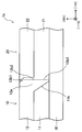
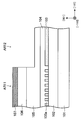
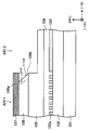
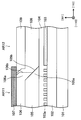
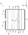
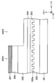
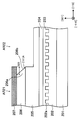
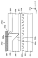
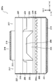
- FIG. 1 It is a figure which shows the structural example of an optical semiconductor integrated element. It is a figure which shows an example of the formation method of an optical semiconductor integrated element. It is a principal part cross-sectional schematic diagram (the 1) of a semiconductor regrowth process. It is a principal part cross-sectional schematic diagram of the semiconductor regrowth process (the 2). It is a principal part cross-sectional schematic diagram of the semiconductor regrowth process (the 3). It is a figure which shows another structural example of an optical semiconductor integrated element. It is a principal part cross-sectional schematic diagram of the 1st semiconductor growth process which concerns on 1st Example. It is a principal part cross-sectional schematic diagram of the 1st etching process which concerns on 1st Example.
- FIG. 1 is a diagram showing a configuration example of an optical semiconductor integrated device. Note that FIG. 1 schematically shows a cross-section of an essential part of an example of an optical semiconductor integrated device.
- An optical semiconductor integrated device 1 shown in FIG. 1 has a first optical semiconductor device 10 and a second optical semiconductor device 20 formed above a substrate 30 having a (001) plane.
- the first optical semiconductor element 10 includes a first core layer 11 including an optical waveguide formed above the (001) plane of the substrate 30 and a first cladding layer 12 formed above the first core layer 11. It is out.
- the second optical semiconductor element 20 includes a second core layer 21 including an optical waveguide formed above the (001) plane of the substrate 30, and a second cladding layer 22 formed above the second core layer 21. It is out.
- the first optical semiconductor element 10 and the second optical semiconductor element 20 are formed using a semiconductor material, and are formed side by side in the [110] direction above the substrate 30.
- the first optical semiconductor element 10 and the second optical semiconductor element 20 are the second core of the second optical semiconductor element 20 after the growth of the first core layer 11 and the first cladding layer 12 of the first optical semiconductor element 10 on the substrate 30.
- the layer 21 and the second cladding layer 22 can be formed using a BJ growth method in which the layer 21 and the second cladding layer 22 are regrown.
- the first core layer 11 of the first optical semiconductor device 10 is formed such that the end surface 11b facing the second optical semiconductor device 20 is inclined.
- the first core layer 11 has an end face 11b having an A-plane orientation on the second optical semiconductor element 20 side.
- the end surface 11b is, for example, a (111) A surface.
- the first cladding layer 12 formed above the first core layer 11 is formed with the end 12 a covering a part of the end surface 11 b of the first core layer 11.
- the surface of the end portion 12a of the first cladding layer 12 is divided into three regions: an upper end surface 12b1, a middle end surface 12b2, and a lower end surface 12b3.
- the upper end face 12b1 of the first cladding layer 12 has an A-plane orientation, for example, a (111) A plane.
- the middle end surface 12b2 connected to the upper end surface 12b1 is a (110) plane having an angle of 90 ° with the (001) plane.
- the lower end surface 12b3 connected to the middle end surface 12b2 is a crystal plane in which the angle ⁇ formed with the (001) plane is in the range of 55 ° to 90 ° (55 ° ⁇ ⁇ ⁇ 90 °).
- ⁇ 55 °
- the lower end surface 12b3 is a (111) B surface.
- the lower end face 12b3 is a crystal face having a B-plane orientation.
- the second optical semiconductor element 20 is formed in the [110] direction of the first optical semiconductor element 10 having such a configuration.
- the second core layer 21 of the second optical semiconductor element 20 is formed so as to cover the side surfaces of the first core layer 11 and the first cladding layer 12 of the first optical semiconductor element 10.
- the case where a part of the second core layer 21 is sandwiched between the first cladding layer 12 and the second cladding layer 22 is illustrated.
- an n-type indium phosphide (InP) substrate can be used as the substrate 30 of the optical semiconductor integrated device 1 as described above.
- AlGaInAs aluminum gallium indium arsenide
- p-type InP can be used for the first core layer 11 of the first optical semiconductor element 10.
- AlGaInAs or gallium indium arsenide phosphorus (GaInAsP) can be used for the second core layer 21 of the second optical semiconductor element 20.
- P-type InP can be used for the second cladding layer 22 of the second optical semiconductor element 20.
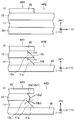
- FIG. 2 is a diagram showing an example of a method for forming an optical semiconductor integrated device.
- 2A is a schematic cross-sectional view of an essential part of an example of a semiconductor growth process
- FIG. 2B is a schematic cross-sectional view of an essential part of an example of a side etching process
- FIG. 2C is a cross-sectional view of an essential part of an example of a heat treatment process. It is a schematic diagram.
- the first core layer 11 of the first optical semiconductor element 10 and A first cladding layer 12 is grown.
- the first core layer 11 and the first cladding layer 12 can be grown by, for example, a metal-organic vapor phase growth (Metal-Organic-Vapor-Phase Epitaxy: MOVPE) method.
- MOVPE Metal-organic vapor phase growth
- a dielectric mask 40 that covers the first optical semiconductor element region AR1 is formed.
- the region in the [110] direction of the first optical semiconductor element region AR1 is exposed from the dielectric mask 40 as the second optical semiconductor element region AR2.
- etching is performed using the dielectric mask 40 as a mask to remove the first core layer 11 and the first cladding layer 12 grown in the second optical semiconductor element region AR2. .
- the removal of the first core layer 11 and the first cladding layer 12 can be performed, for example, by wet etching or by wet etching after dry etching. Side etching of the first core layer 11 and the first cladding layer 12 is advanced by wet etching. In the wet etching, for example, the first cladding layer 12 is first selectively etched (side etching), and then the first core layer 11 is selectively etched (side etching).
- the side etching amounts S1 and S2 of the first core layer 11 and the first cladding layer 12 can be controlled by the etching conditions such as the material of the first core layer 11 and the first cladding layer 12, the kind of etchant, the etching time, and the like. it can.
- the end surfaces 12b and 11b having the A-plane orientation are exposed at the end portions 12a and 11a of the first cladding layer 12 and the first core layer 11, respectively.
- the (111) A plane is exposed on the end face 12 b of the first cladding layer 12, and the (111) A plane is exposed on the end face 11 b of the first core layer 11.
- heat treatment is performed.
- the heat treatment can be performed, for example, by heating in the temperature raising process and the temperature holding process until the growth starts when the second core layer 21 is grown in the second optical semiconductor element region AR2.
- a heat treatment may be performed separately from the growth of the second core layer 21, and after the heat treatment, the second core layer 21 may be grown (from temperature increase to growth).
- a mass transport is generated at the end 12a of the first cladding layer 12 as shown in FIG.
- the end 12a of the first cladding layer 12 is inclined so that the end surface 12b exposes the A-plane by side etching before heat treatment, and the first core layer 11 is also side-etched.
- the lower side of the end 12a is a space. That is, the end 12 a of the first cladding layer 12 has a shape protruding like a ridge from the first core layer 11 before the heat treatment.
- the end 12a having such a shape is likely to be in a thermally unstable state when heated, and the end 12a side of the first core layer 11 at the end 12a is more stable. Mass transport occurs. As a result of the mass transport, as shown in FIG. 2C, the corner of the tip of the end 12a disappears, and in addition to the end face 12b (upper end face 12b1), the middle end face 12b2 of the (110) plane, and ( The lower end face 12b3 having an angle of ⁇ with the (001) plane is generated.
- the mass transport amount can be controlled by conditions during heat treatment, such as temperature and time. As the heat treatment conditions are such that the mass transport amount is likely to increase, the shape of the end portion 12a gradually changes as shown by the arrow in FIG. 2C, and the (110) surface is formed on the middle end surface 12b2. As it appears, the angle ⁇ of the lower end surface 12b3 increases. When the angle ⁇ of the lower end surface 12b3 becomes 90 °, the lower end surface 12b3 becomes the (110) surface like the middle end surface 12b2, and further progress of mass transport is suppressed.
- the amount of mass transport in the heat treatment after such side etching is controlled, and the angle ⁇ of the lower end face 12b3 is controlled in the range of 55 ° ⁇ ⁇ ⁇ 90 °.
- FIG. 4 is a schematic cross-sectional view of a relevant part of a semiconductor regrowth process when the temperature is.
- the growth of the second core layer 21 and the growth of the second cladding layer 22 are performed in the second optical semiconductor element region AR2 from the respective states of FIG. 3, FIG. 4, or FIG. 5 obtained after the heat treatment.
- the second core layer 21 and the second cladding layer 22 can be grown by, for example, the MOVPE method.
- the second core layer 21 and the second cladding layer 22 have an angle ⁇ formed by the (001) plane of the lower end face 12b3 formed by mass transport of 40 °. Describe growth.
- the second core layer 21 grows above the substrate 30 and also on the side surface of the first optical semiconductor element 10 in the second optical semiconductor element region AR2. That is, the second core layer 21 also grows on the end face 11b of the first core layer 11 and the upper end face 12b1, the middle end face 12b2, and the lower end face 12b3 of the first cladding layer 12.
- a B surface having a relatively small angle ⁇ such as 40 ° is exposed like the lower end surface 12b3 of FIG. 5
- the BJ portion of the first optical semiconductor element 10 and the second optical semiconductor element 20 is exposed.
- a stacking fault 50 may occur.
- This stacking fault 50 is the growth of the second core layer 21 in which the growth surface of the second core layer 21 growing along the lower end surface 12b3 of the B surface grows along the end surface 11b of the A surface of the first core layer 11. It is thought to be generated by colliding with the surface.
- the stacking fault 50 may also be generated in the second cladding layer 22. is there.
- abnormal growth occurs in the BJ portions of the first optical semiconductor element 10 and the second optical semiconductor element 20. May occur. Such abnormal growth causes an increase in the film thickness of the BJ portion of the first optical semiconductor element 10 and the second optical semiconductor element 20, resulting in a change in the refractive index of the BJ portion, thereby degrading initial characteristics such as light output. There is a possibility to make it.
- the second core layer 21 Collisions between the growth surfaces during growth can be suppressed. That is, the growth surface of the second core layer 21 that grows along the (110) plane of the middle end face 12b2 and the lower end face 12b3 and the second core layer 21 that grows along the end face 11b of the A surface of the first core layer 11. Collision with the growth surface is suppressed, and the occurrence of the stacking fault 50 as described above is suppressed. Accordingly, the second cladding layer 22 that subsequently grows can also be grown while suppressing the occurrence of the stacking fault 50. Further, in the growth of the second core layer 21 and the second cladding layer 22 from the state as shown in FIG. 3, the occurrence of abnormal growth can be suppressed.
- the second cladding layer 22 that subsequently grows can also be grown while suppressing the occurrence of the stacking fault 50. Further, in the growth of the second core layer 21 and the second cladding layer 22 from the state as shown in FIG. 4, the occurrence of abnormal growth can be suppressed.
- the case where the end 12a of the first cladding layer 12 on the first optical semiconductor element 10 side covers a part of the end surface 11b of the first core layer 11 is described as an example.
- the entire end surface 11 b of the first core layer 11 may be covered with the end 12 a of the cladding layer 12.
- FIG. 6 is a diagram showing another configuration example of the optical semiconductor integrated device.
- FIG. 6 schematically shows a cross section of an essential part of an example of the optical semiconductor integrated device.
- the optical semiconductor integrated device 1 a shown in FIG. 6 has a structure in which the entire end surface 11 b of the first core layer 11 on the first optical semiconductor device 10 side is covered with the end 12 a of the first cladding layer 12.
- the other configuration is the same as that of the optical semiconductor integrated device 1 here.
- the end portion 12a of the first cladding layer 12 has an upper end surface 12b1 of the A surface, a middle end surface 12b2 and a lower end surface 12b3 of the (110) plane (that is, the angle ⁇ is 90 °).
- the side etching amount S1 of the first core layer 11 is changed to the side etching amount S2 of the first cladding layer 12 by side etching at the time of forming the first optical semiconductor element 10.
- it is made larger than the case of FIG. In this way, during the subsequent heat treatment, more mass transport proceeds at the end 12a, and a structure in which the entire end surface 11b of the first core layer 11 is covered with the end 12a after mass transport is obtained. Is possible.
- the side etching of the first cladding layer 12 is performed in the step of FIG. 2B, but the side etching of the first cladding layer 12 is not necessarily performed. Even if the side etching of the first cladding layer 12 is not performed, if the side etching of the first core layer 11 is performed, the mass transport of the first cladding layer 12 is generated by the subsequent heat treatment.
- the second optical semiconductor element 20 side It is possible to suppress the occurrence of defects such as stacking faults even during regrowth.
- the BJ junction in which defects such as stacking faults are suppressed is formed by selective wet etching of the first cladding layer 12 and the first core layer 11, for example. be able to. In that case, it becomes possible to obtain high reproducibility for the etched shape of the side surface or bottom of the first cladding layer 12 and the first core layer 11.
- the heat treatment for causing the mass transport of the first cladding layer 12 can be performed, for example, in a reactor of the MOVPE apparatus when the second core layer 21 is grown. 21 can grow. In that case, it becomes possible to obtain a BJ junction in which defects such as stacking faults are suppressed without increasing the number of steps.
- a modulator integrated laser optical semiconductor integrated element
- a laser optical semiconductor element
- a modulator optical semiconductor element
- a modulator integrated type laser will be described in accordance with its formation process.
- FIG. 7 is a schematic cross-sectional view of the relevant part showing a first semiconductor growth step according to the first embodiment.
- a semiconductor layer constituting a laser is formed on an n-InP (001) substrate 101.
- the semiconductor layer can be grown using the MOVPE method.
- an n-InP buffer layer 102 having a carrier concentration of 5 ⁇ 10 17 cm ⁇ 3 is grown on an n-InP (001) substrate 101.
- an n-InGaAsP layer 103 having a carrier concentration of 5 ⁇ 10 17 cm ⁇ 3 , a composition wavelength of 1.1 ⁇ m, and a thickness of 100 nm is grown on the n-InP buffer layer 102.
- an n-InP cap layer having a carrier concentration of 5 ⁇ 10 17 cm ⁇ 3 and a thickness of 10 nm is grown on the n-InGaAsP layer 103.
- an n-InP spacer layer 104 having a thickness of 100 nm is grown to fill the diffraction grating 103a in a temperature region where the formed diffraction grating 103a does not undergo thermal deformation.
- an AlGaInAs optical confinement layer (SCH layer) 105A having a composition wavelength of 1.1 ⁇ m and a thickness of 50 nm is grown.
- the growth of the AlGaInAs barrier layer 105B having a composition wavelength of 1.1 ⁇ m and a thickness of 10 nm and the AlGaInAs well layer 105C having a composition wavelength of 1.45 ⁇ m and a thickness of 5 nm are repeated (for example, a total of 10 periods), and AlGaInAs multiple layers are obtained.
- a quantum well layer is formed.
- an AlGaInAs light confinement layer 105A having a composition wavelength of 1.1 ⁇ m and a thickness of 50 nm is grown. Thereby, the AlGaInAs core layer 105 is formed.
- FIG. 8 is a schematic sectional view showing an important part of the first etching process according to the first embodiment.
- a dielectric mask 107 is formed in the laser region AR11.
- the dielectric mask 107 has a pattern shape extending in the [110] direction and having a width of 20 ⁇ m and a length of 300 ⁇ m, and is formed at intervals of 600 ⁇ m in the [110] direction.
- the dielectric mask 107 is made of, for example, silicon oxide (SiO 2 ).
- the p-InP cladding layer 106 and the AlGaInAs core layer 105 in the modulator region AR12 are etched halfway through the AlGaInAs core layer 105, for example, to a depth of about 280 nm.
- FIG. 9 is a schematic sectional view showing an important part of a second etching process according to the first embodiment.
- the p-InP cladding layer 106 is wet etched.
- the p-InP clad layer 106 is selectively etched using a bromine (Br) etchant.
- the p-InP cladding layer 106 is side-etched so that the side etching amount S12 of the end portion 106a of the p-InP cladding layer 106 is about 100 nm.
- the end surface 106b of the p-InP clad layer 106 is in a state where the (111) A surface is exposed.
- a ridge of the dielectric mask 107 is formed on the p-InP clad layer 106.
- the wrinkles of the dielectric mask 107 play a role of suppressing the semiconductor from creeping up and growing on the dielectric mask 107 during the growth of a semiconductor layer constituting the modulator described later.
- FIG. 10 is a schematic sectional view showing an important part of a third etching process according to the first embodiment.
- wet etching of the AlGaInAs core layer 105 is performed.
- the AlGaInAs core layer 105 is selectively etched using a mixed solution of dilute sulfuric acid and hydrogen peroxide solution as an etchant.
- the AlGaInAs core layer 105 is side-etched so that the side etching amount S11 of the end portion 105a of the AlGaInAs core layer 105 is about 120 nm.
- the end surface 105b of the AlGaInAs core layer 105 is in a state where the (111) A surface is exposed.
- the n-InP spacer layer 104 under the AlGaInAs core layer 105 is exposed in the modulator region AR12.
- the etching of the n-InP spacer layer 104 can be suppressed, and the AlGaInAs core layer 105 can be selectively etched with a predetermined side etching amount S11.
- FIG. 11 is a schematic sectional view showing an important part of a heat treatment process according to the first embodiment. After wet etching of the p-InP clad layer 106 and the AlGaInAs core layer 105, heat treatment is performed to generate a mass transport of the end portion 106a of the p-InP clad layer 106.
- the substrate after wet etching is set in the reactor of the MOVPE apparatus, and the temperature is raised to 690 ° C. in a PH 3 atmosphere.
- the (111) A plane remains at the upper portion and the (001) plane below it at the end portion 106a of the p-InP cladding layer 106 (001).
- the upper part of the end face 105b of the AlGaInAs core layer 105 is covered with the end part 106a after the mass transport of the p-InP clad layer 106, and the lower part remains with the (111) A face exposed.
- a (110) plane on the side surface of the p-InP cladding layer 106 is formed continuously with the end face 105 b of the AlGaInAs core layer 105.
- Such a side surface shape of the p-InP clad layer 106 is obtained by appropriately setting the above-described side etching amounts S11 and S12 (FIGS. 9 and 10) and generating sufficient mass transport by heat treatment (FIG. 11). ),Obtainable.
- FIG. 12 is a schematic cross-sectional view of the relevant part showing a second semiconductor growth step according to the first embodiment.
- an AlGaInAs optical confinement layer having a composition wavelength of 1.2 ⁇ m and a thickness of 50 nm is first grown. Subsequently, the growth of an AlGaInAs barrier layer having a composition wavelength of 1.2 ⁇ m and a thickness of 5 nm and an AlGaInAs well layer having a composition wavelength of 1.35 ⁇ m and a thickness of 10 nm are repeated (for example, a total of 10 periods) to obtain an AlGaInAs multiple quantum well Form a layer. Further, an AlGaInAs optical confinement layer having a composition wavelength of 1.2 ⁇ m and a thickness of 50 nm is grown.
- a p-InP layer having a carrier concentration of 5 ⁇ 10 17 cm ⁇ 3 and a thickness of 150 nm is grown.
- the crystal planes exposed on the side surface on the laser region AR11 side are the (111) A plane and the (110) plane, so collision between the growth planes is avoided and stacking faults are generated. Can be suppressed.
- the p-InP clad layer 109 in which the occurrence of stacking faults and the like is suppressed can be formed.
- the AlGaInAs core layer 108 and the p-InP cladding layer 109 can be grown in a region below the dielectric mask 107 by setting the dielectric mask 107 as a ridge as described above.
- the growth of the AlGaInAs core layer 108 and the p-InP clad layer 109 can be performed in the same MOVPE apparatus following the heat treatment for generating mass transport in the end portion 106a of the p-InP clad layer 106.
- the heat treatment can also serve as a temperature raising step and a temperature holding step before starting the growth of the AlGaInAs core layer 108 (before introducing the raw material). Accordingly, it is possible to suppress an increase in the number of steps for forming the end portion 106a of the p-InP cladding layer 106 as shown in FIG.
- the basic structure of the laser and the basic structure of the modulator are arranged on the n-InP (001) substrate 101 in the [110] direction and optically connected. In this state, a joined structure (BJ structure) is obtained.
- FIG. 13 is a schematic sectional view showing an important part of a third semiconductor growth step according to the first embodiment. After the basic structures of the laser and the modulator are formed as shown in FIGS. 7 to 12, first, the dielectric mask 107 is removed, and a predetermined semiconductor layer is grown.
- a p-InP cladding layer 110 having a carrier concentration of 1 ⁇ 10 18 cm ⁇ 3 and a thickness of 1.5 ⁇ m is first grown on the substrate after removal of the dielectric mask 107.
- a p-InGaAs contact layer 111 having a carrier concentration of 1 ⁇ 10 19 cm ⁇ 3 and a thickness of 0.5 ⁇ m is grown.
- FIG. 14 is a schematic cross-sectional view of the relevant part showing a buried layer forming step according to the first embodiment.
- FIG. 14 schematically shows a cross section when the laser region AR11 is viewed in the [110] direction.
- a mask 113 is formed. For convenience, although illustration is omitted here, a plurality of masks 113 may be formed in stripes.
- etching is performed to form a groove 114 reaching the n-InP (001) substrate 101, and a mesa 115 having a height of 3 ⁇ m is formed. Then, both sides of the mesa 115 are buried with an InP layer doped with iron (Fe) to form a buried layer 112 as shown in FIG.
- FIG. 15 is a schematic sectional view showing an important part of an optical semiconductor integrated device according to the first embodiment.
- the p-InGaAs contact layer 111 is separated into the laser 116 side and the modulator 117 side, and a p-side electrode 118 is formed on each p-InGaAs contact layer 111.
- the p-side electrode 118 is formed on the p-InGaAs contact layer 111, and then the p-side electrode 118 and the p-InGaAs contact layer 111 are separated.
- An n-side electrode 119 is formed on the back surface of the n-InP (001) substrate 101.
- the cleavage is performed.
- an array of modulator integrated lasers 100 is obtained.
- the array may be further cleaved into chips including a predetermined number of modulator integrated lasers 100.
- a distributed feedback (DRB) laser distributed feedback (DFB) laser (optical semiconductor element) and a distributed Bragg reflector (DBR) (optical semiconductor element) are integrated.
- DBR distributed Bragg reflector
- An optical semiconductor integrated device will be described as an example.
- such a DR laser will be described in accordance with its formation process.
- FIG. 16 is a schematic sectional view showing an important part of a first semiconductor growth step according to the second embodiment.
- a semiconductor layer constituting a DFB laser is formed on an n-InP (001) substrate 201.
- the semiconductor layer can be grown using the MOVPE method.
- an n-InP buffer layer 202 having a carrier temperature of 5 ⁇ 10 17 cm ⁇ 3 and a thickness of 300 nm is grown on an n-InP (001) substrate 201 at a growth temperature of 630 ° C. Then, resist coating, electron beam exposure, development, and etching are performed to form a diffraction grating 202a having a pitch of 200 nm and a depth of 50 nm in the n-InP buffer layer 202 in the DFB laser region AR21 and the DBR region AR22.
- an n-InGaAsP layer 203 having a carrier concentration of 5 ⁇ 10 17 cm ⁇ 3 and a composition wavelength of 1.1 ⁇ m is grown, and the diffraction formed on the n-InP buffer layer 202 Fill the grid 202a.
- an n-InP spacer layer 204 having a thickness of 20 nm is grown on the n-InGaAsP layer 203.
- an AlGaInAs light confinement layer 205A having a composition wavelength of 1.1 ⁇ m and a thickness of 30 nm is grown.
- the growth of the AlGaInAs barrier layer 205B having a composition wavelength of 1.1 ⁇ m and a thickness of 10 nm and the AlGaInAs well layer 205C having a composition wavelength of 1.1 ⁇ m and a thickness of 5 nm are repeated (for example, a total of five periods), and AlGaInAs multiple layers are obtained.
- a quantum well layer is formed.
- an AlGaInAs light confinement layer 205A having a composition wavelength of 1.1 ⁇ m and a thickness of 30 nm is grown. Thereby, the AlGaInAs core layer 205 is formed.
- FIG. 17 is a schematic sectional view showing an important part of a first etching process according to the second embodiment.
- a dielectric mask 207 such as SiO 2 ) is formed in the DFB laser region AR21.
- the dielectric mask 207 has a pattern shape extending in the [110] direction and having a width of 20 ⁇ m and a length of 300 ⁇ m, and is formed at intervals of 100 ⁇ m in the [110] direction.
- dry etching of the DBR region AR22 is performed using the dielectric mask 207 as a mask.
- the p-InP cladding layer 206 and the AlGaInAs core layer 205 in the DBR region AR22 are etched halfway through the AlGaInAs core layer 205, for example, to a depth of about 270 nm.
- FIG. 18 is a schematic sectional view showing an important part of a second etching process according to the second embodiment.
- the p-InP cladding layer 206 is wet etched.
- the p-InP cladding layer 206 is selectively etched using a Br-based etchant.
- the p-InP cladding layer 206 is side-etched so that the side etching amount S22 of the end portion 206a of the p-InP cladding layer 206 is about 130 nm.
- the end surface 206b of the p-InP clad layer 206 is in a state where the (111) A surface is exposed.
- a ridge of the dielectric mask 207 is formed on the p-InP clad layer 206, thereby causing a creeping of the semiconductor grown later on the dielectric mask 207. It will be suppressed.
- FIG. 19 is a schematic sectional view showing an important part of a third etching process according to the second embodiment.
- the AlGaInAs core layer 205 is wet etched.
- the AlGaInAs core layer 205 is selectively etched using a mixed solution of dilute sulfuric acid and hydrogen peroxide solution as an etchant.
- the AlGaInAs core layer 205 is side-etched so that the side etching amount S21 of the end portion 205a of the AlGaInAs core layer 205 is about 400 nm.
- the end face 205b of the AlGaInAs core layer 205 is in a state where the (111) A face is exposed.
- the n-InP spacer layer 204 under the AlGaInAs core layer 205 is exposed.
- the etching of the n-InP spacer layer 204 can be suppressed, and the AlGaInAs core layer 205 can be selectively etched with a predetermined side etching amount S21.
- FIG. 20 is a schematic sectional view showing an important part of a heat treatment process according to the second embodiment. After wet etching of the p-InP clad layer 206 and the AlGaInAs core layer 205, heat treatment is performed to generate a mass transport at the end 206a of the p-InP clad layer 206.
- the substrate after wet etching is set in the reactor of the MOVPE apparatus, and the temperature is raised to 690 ° C. in a PH 3 atmosphere.
- the (111) A plane remains at the upper part and the (001) plane below it at the end part 206a of the p-InP cladding layer 206.
- the (110) plane whose angle to the plane is 90 ° appears.
- the AlGaInAs core layer 205 is entirely covered with the end portion 206 a of the p-InP clad layer 206 after the mass transport of the (111) A surface of the end surface 205 b.
- Such a side surface shape of the p-InP clad layer 206 causes the protrusion amount of the p-InP clad layer 206 from the AlGaInAs core layer 205 to be relatively large at the side etching stage, and a sufficient mass transport is generated by the heat treatment. Can be obtained.
- FIG. 21 is a schematic cross-sectional view of the relevant part showing a second semiconductor growth step according to the second embodiment.
- the AlGaInAs waveguide layer 208 having a composition wavelength of 1.2 ⁇ m and a thickness of 145 nm, and an undoped iP in the DBR region AR22.
- -InP cladding layer 209 is grown.
- the i-InP clad layer 209 in which the occurrence of stacking faults and the like is suppressed can be formed.
- the AlGaInAs waveguide layer 208 and the i-InP clad layer 209 can be grown in a region below the dielectric mask 207 by the dielectric mask 207.
- the heat treatment for generating mass transport at the end portion 206a of the p-InP clad layer 206 also serves as a temperature raising step and a temperature holding step before starting the growth of the AlGaInAs waveguide layer 208 (before introducing the raw material). be able to.
- the basic structure of the DFB laser and the basic structure of the DBR are arranged on the n-InP (001) substrate 101 in the [110] direction to be optically connected. In this state, a joined structure (BJ structure) is obtained.
- FIG. 22 is a schematic sectional view showing an important part of an optical semiconductor integrated device according to the second embodiment.
- the dielectric mask 207 is removed.
- the carrier concentration is 1 ⁇ 10 18 cm ⁇ 3 and the thickness is 1
- a p-InP cladding layer 210 having a thickness of 5 ⁇ m is grown.
- a p-InGaAs contact layer 211 having a carrier concentration of 1 ⁇ 10 19 cm ⁇ 3 and a thickness of 0.5 ⁇ m is grown.
- one or a plurality of masks having a width of 1.5 ⁇ m and extending in the [110] direction so as to cover regions corresponding to both basic structures of the DFB laser and the DBR are formed in a stripe shape. Then, dry etching is performed to form a mesa having a height of 3 ⁇ m. Both sides of the mesa are embedded with an Fe-doped InP layer.
- the array is further formed into a chip including a predetermined number of DR lasers 200. You just have to cleave it.
- the AlGaInAs waveguide layer 208 is formed.
- a GaInAsP waveguide layer may be formed. The first embodiment and the second embodiment have been described above.
- the (111) A plane remains above the end portions 106a and 206a of the p-InP cladding layers 106 and 206.
- a case where a (110) plane having an angle of 90 ° with the (001) plane is formed is illustrated.
- a crystal plane having an angle of 55 ° or more and less than 90 ° with the (001) plane may exist.
- FIG. 23 shows a schematic cross-sectional view of an essential part of another example of the heat treatment process according to the second embodiment.
- InP mass transport can be generated by heat treatment after side etching, and the side surface of the p-InP cladding layer 206 can be shaped as shown in FIG. That is, in the example of FIG. 23, the (111) A surface remains on the upper end surface 206b1 and the (110) surface is formed on the middle end surface 206b2 by InP mass transport.
- the lower end face 206b3 is formed with a crystal plane having an angle ⁇ with the (001) plane in a range of 55 ° ⁇ ⁇ ⁇ 90 °.
- the side shape of the p-InP cladding layer 106 after heat treatment is as follows: (111) A surface at the upper end surface, (110) surface at the middle end surface, and (001) at the lower end surface. It is also possible to adopt a shape in which there is a crystal plane whose angle ⁇ formed with the plane is in the range of 55 ° ⁇ ⁇ ⁇ 90 °. Thereby, generation
- the BJ structure in which two functional elements are arranged in the [110] direction and bonded to each optical semiconductor integrated element is illustrated. That is, the case where one BJ portion exists for one optical semiconductor integrated device has been illustrated.
- the above technique can be similarly applied to a case where a plurality of BJ portions exist in one optical semiconductor integrated device.
- FIG. 24 shows a configuration example of an optical semiconductor integrated device in such a case.
- FIG. 24 illustrates a DR laser 200a as an optical semiconductor integrated device.
- DBRs 217 are formed on both sides of one DFB laser 216, respectively. That is, DBRs 217 are formed at the entrance end and the exit end of the DFB laser 216, respectively.
- These three elements, that is, the DBR 217, the DR laser 200a, and the DBR 217 are formed side by side in the [110] direction.
- Such a DR laser 200a can be formed according to the example of the second embodiment.
- the DBR region AR22 sandwiching the DFB laser region AR21 in the [110] direction is etched.
- the both side surfaces in the [110] direction of the DFB laser region AR21 are formed into a shape having a predetermined crystal plane by heat treatment.
- the DBR region AR22 is regrown.
- the p-InP cladding layer 210, the p-InGaAs contact layer 211, the p-side electrode 218, the n-side electrode 219, and the non-reflective film 220 may be formed in the same manner as in the second embodiment.
- the AlGaInAs core layers 105 and 205 including the multiple quantum well layers are illustrated.
- a bulk structure, a quantum wire structure, and a quantum dot structure are used. It is also possible to apply the core layer used.
- the case where the n-InP (001) substrates 101 and 201 are used is exemplified.
- a p-type substrate, semi-insulating (SI) is used. It is also possible to apply a substrate.
- the structure of the n layer, the arrangement of the electrodes, etc. are arbitrary so that carriers can be supplied to the n layer provided under the core layer. Be changed.
- an optical semiconductor module can be formed by combining the optical semiconductor integrated device as described in the first and second embodiments with other devices.
- an optical semiconductor module using the DR laser 200 described in the second embodiment is shown in FIG.
- the DR laser 200 is mounted on a coaxial package 302 having lead pins 301. Further, a light receiving element 303 for back monitoring is installed on the rear end face side of the DR laser 200. Each lead pin 301 is connected to the DR laser 200 or the light receiving element 303.
- the lead pin 301 connected to the DR laser 200 is connected to an electric signal source that drives the DFB laser.
- the lead pin 301 connected to the light receiving element 303 is connected to a monitor device that monitors the output of the DR laser 200.
- the DR laser 200 and the light receiving element 303 are covered with a cap 305 provided with a lens 304.
- the lens 304 functions as an optical output port that condenses the laser light (signal light) emitted from the front end face of the DR laser 200 and makes it incident on an optical fiber provided at the tip.
- the optical semiconductor module 300 does not include a thermoelectric cooling element that adjusts the temperature of the DR laser 200. This is because since the DR laser 200 has an AlGaInAs-based active layer, the DR laser 200 oscillates in a longitudinal single mode over a wide temperature range.
- optical semiconductor module equipped with a DR laser has been illustrated, but various optical semiconductor integrated elements such as modulator integrated lasers are combined with other elements to form optical semiconductor modules in a form suitable for each application. Is possible.
- Optical semiconductor integrated device 10 1st optical semiconductor device 11 1st core layer 12 1st clad layer 11a, 12a, 105a, 106a, 205a, 206a End part 11b, 12b, 105b, 106b, 205b, 206b End surface 12b1, 206b1 Upper end face 12b2, 206b2 Middle end face 12b3, 206b3 Lower end face 20 Second optical semiconductor element 21 Second core layer 22 Second clad layer 30 Substrate 40, 107, 207 Dielectric mask 50 Stacking fault 100 Modulator integrated laser 101, 201 n-InP (001) substrate 102, 202 n-InP buffer layer 103, 203 n-InGaAsP layer 103a, 202a diffraction grating 104, 204 n-InP spacer layer 105, 108, 205 AlGaInAs core layer 105A, 205A Al aInAs light confine
Landscapes
- Physics & Mathematics (AREA)
- Optics & Photonics (AREA)
- Condensed Matter Physics & Semiconductors (AREA)
- General Physics & Mathematics (AREA)
- Electromagnetism (AREA)
- Nanotechnology (AREA)
- Chemical & Material Sciences (AREA)
- Engineering & Computer Science (AREA)
- Geometry (AREA)
- Biophysics (AREA)
- Crystallography & Structural Chemistry (AREA)
- Life Sciences & Earth Sciences (AREA)
- Semiconductor Lasers (AREA)
- Optical Couplings Of Light Guides (AREA)
- Optical Integrated Circuits (AREA)
Abstract
光半導体集積素子の信頼性及び性能の向上を図る。 光半導体集積素子(1)は、基板(30)の(001)面上方に形成された第1光半導体素子(10)と、基板(30)の(001)面上方で、第1光半導体素子(10)の[110]方向に、第1光半導体素子(10)と光学的に接続されて形成された第2光半導体素子(20)とを含む。第1光半導体素子(10)は、第1コア層(11)と、第1コア層(11)上方に形成され、第2光半導体素子(20)側の側面に、(001)面となす角度θが55°以上90°以下の結晶面を有する第1クラッド層(12)とを含む。
Description
本発明は、光半導体集積素子及びその製造方法に関する。
光ファイバ通信において、複数の光半導体素子を単一基板上に集積した光半導体集積素子は、光モジュールの小型化の観点から有効である。
従来、このように複数の光半導体素子を単一基板上に集積する手法の1つとして、基板上に一の光半導体素子構造を成長した後、その一部を除去し、その除去した部分に他の光半導体素子構造を選択的に再成長する、バットジョイント(Butt Joint:BJ)成長法が知られている。
従来、このように複数の光半導体素子を単一基板上に集積する手法の1つとして、基板上に一の光半導体素子構造を成長した後、その一部を除去し、その除去した部分に他の光半導体素子構造を選択的に再成長する、バットジョイント(Butt Joint:BJ)成長法が知られている。
上記のようなBJ成長法では、各光半導体素子の独立設計が可能であるという利点がある。しかし、BJ成長法を用いて形成される光半導体集積素子には、光半導体素子間の接合部(BJ部)に発生する結晶欠陥或いは異常成長により、光半導体集積素子の信頼性が低下したり、初期特性が劣化したりするといった問題が生じる場合があった。
本発明の一観点によれば、基板の(001)面上方に形成された第1光半導体素子と、前記基板の(001)面上方で、前記第1光半導体素子の[110]方向に、前記第1光半導体素子と光学的に接続されて形成された第2光半導体素子と、を含み、前記第1光半導体素子は、第1コア層と、前記第1コア層上方に形成され、前記第2光半導体素子側の側面に、(001)面となす角度が55°以上90°以下の第1結晶面を有する第1クラッド層とを含む光半導体集積素子が提供される。
開示の光半導体集積素子によれば、光半導体素子間の結晶欠陥、異常成長が抑えられ、その信頼性及び性能の向上が図られる。
本発明の上記及び他の目的、特徴及び利点は本発明の例として好ましい実施の形態を表す添付の図面と関連した以下の説明により明らかになるであろう。
本発明の上記及び他の目的、特徴及び利点は本発明の例として好ましい実施の形態を表す添付の図面と関連した以下の説明により明らかになるであろう。
図1は光半導体集積素子の構成例を示す図である。尚、図1には、光半導体集積素子の一例の要部断面を模式的に図示している。
図1に示す光半導体集積素子1は、(001)面を有する基板30上方に形成された第1光半導体素子10及び第2光半導体素子20を有している。
図1に示す光半導体集積素子1は、(001)面を有する基板30上方に形成された第1光半導体素子10及び第2光半導体素子20を有している。
第1光半導体素子10は、基板30の(001)面上方に形成された、光導波路を含む第1コア層11と、第1コア層11上方に形成された第1クラッド層12とを含んでいる。第2光半導体素子20は、基板30の(001)面上方に形成された、光導波路を含む第2コア層21と、第2コア層21上方に形成された第2クラッド層22とを含んでいる。
第1光半導体素子10及び第2光半導体素子20は、半導体材料を用いて形成され、また、基板30上方において[110]方向に並んで形成されている。第1光半導体素子10及び第2光半導体素子20は、基板30に第1光半導体素子10の第1コア層11及び第1クラッド層12の成長後に、第2光半導体素子20の第2コア層21及び第2クラッド層22を再成長する、BJ成長法を用いて形成することができる。
上記のような光半導体集積素子1において、第1光半導体素子10の第1コア層11は、第2光半導体素子20と対向する端面11bが、傾斜して形成されている。第1コア層11は、第2光半導体素子20側に、A面方位を有する端面11bを有している。端面11bは、例えば、(111)A面である。
第1コア層11上方に形成される第1クラッド層12は、この図1の例では、端部12aが、第1コア層11の端面11bの一部を覆った状態で形成されている。ここでは説明の便宜上、第1クラッド層12の端部12a表面を、上部端面12b1、中部端面12b2、下部端面12b3の3領域に分ける。
第1クラッド層12の上部端面12b1は、A面方位を有し、例えば、(111)A面である。上部端面12b1に連なる中部端面12b2は、(001)面とのなす角度が90°である、(110)面である。中部端面12b2に連なる下部端面12b3は、(001)面となす角度θが55°以上90°以下(55°≦θ≦90°)の範囲にある結晶面である。尚、図1中、実線で示した下部端面12b3は、θ=90°の場合を表しており、この場合、下部端面12b3は、中部端面12b2と同じく(110)面となる。また、θ=55°の場合、下部端面12b3は、(111)B面となる。55°≦θ<90°の範囲では、下部端面12b3は、B面方位を有する結晶面となる。
このような構成を有する第1光半導体素子10の[110]方向に、第2光半導体素子20が形成されている。図1には、第2光半導体素子20の第2コア層21が、第1光半導体素子10の第1コア層11及び第1クラッド層12の側面を覆うように形成され、第1クラッド層12と第2クラッド層22の間に第2コア層21の一部が挟まれている場合を例示している。
尚、上記のような光半導体集積素子1の基板30には、例えば、n型インジウムリン(InP)基板を用いることができる。第1光半導体素子10の第1コア層11には、例えば、アルミニウムガリウムインジウムヒ素(AlGaInAs)を用いることができる。第1光半導体素子10の第1クラッド層12には、p型InPを用いることができる。第2光半導体素子20の第2コア層21には、AlGaInAs、又はガリウムインジウムヒ素リン(GaInAsP)を用いることができる。第2光半導体素子20の第2クラッド層22には、p型InPを用いることができる。
図1に示すような光半導体集積素子1は、例えば、次のような方法で形成される。
図2は光半導体集積素子の形成方法の一例を示す図である。図2(A)は半導体成長工程の一例の要部断面模式図、図2(B)はサイドエッチング工程の一例の要部断面模式図、図2(C)は熱処理工程の一例の要部断面模式図である。
図2は光半導体集積素子の形成方法の一例を示す図である。図2(A)は半導体成長工程の一例の要部断面模式図、図2(B)はサイドエッチング工程の一例の要部断面模式図、図2(C)は熱処理工程の一例の要部断面模式図である。
まず、図2(A)に示すように、基板30上方の、第1光半導体素子領域AR1、及び第2光半導体素子領域AR2の双方に、第1光半導体素子10の第1コア層11及び第1クラッド層12を成長する。第1コア層11及び第1クラッド層12は、例えば、有機金属気相成長(Metal Organic Vapor Phase Epitaxy:MOVPE)法により成長することができる。
そして、図2(A)に示したように、第1光半導体素子領域AR1を覆う誘電体マスク40を形成する。第1光半導体素子領域AR1の[110]方向の領域を、第2光半導体素子領域AR2として誘電体マスク40から露出させる。
次いで、図2(B)に示すように、誘電体マスク40をマスクにしてエッチングを行い、第2光半導体素子領域AR2に成長されている第1コア層11及び第1クラッド層12を除去する。
第1コア層11及び第1クラッド層12の除去は、例えば、ウェットエッチングで、又はドライエッチング後にウェットエッチングすることで、行うことができる。ウェットエッチングにより、第1コア層11及び第1クラッド層12のサイドエッチングを進行させる。ウェットエッチングでは、例えば、まず第1クラッド層12を選択的にエッチング(サイドエッチング)し、次いで第1コア層11を選択的にエッチング(サイドエッチング)する。第1コア層11、第1クラッド層12のサイドエッチング量S1,S2はそれぞれ、第1コア層11及び第1クラッド層12の材質、エッチャントの種類、エッチング時間等、エッチング条件によって制御することができる。
このようなサイドエッチングにより、図2(B)に示したように、第1クラッド層12、第1コア層11の端部12a,11aに、A面方位を有する端面12b,11bをそれぞれ表出させる。例えば、第1クラッド層12の端面12bに(111)A面を表出させ、第1コア層11の端面11bにも(111)A面を表出させる。
サイドエッチング後は、熱処理を行う。熱処理は、例えば、第2光半導体素子領域AR2に第2コア層21を成長する際の、その成長を開始するまでの間の昇温過程及び温度保持過程の加熱により行うことができる。また、第2コア層21の成長とは別に熱処理を行っておき、その熱処理後、第2コア層21の成長(昇温から成長)を行うようにしてもよい。
尚、第1コア層11及び第1クラッド層12としてIII-V族化合物半導体を成長している場合には、熱処理の際、V族元素を含む雰囲気で熱処理を行うことが望ましい。これは、V族元素の方がIII族元素に比べて蒸気圧が高いため、III-V族化合物半導体からのV族元素の消失を抑えるためである。例えば、第1コア層11にAlGaInAs、第1クラッド層12にInPを用いている場合には、ホスフィン(PH3)雰囲気で熱処理を行う。
サイドエッチング後に熱処理を行うことで、図2(C)に示すように、第1クラッド層12の端部12aにマストランスポートを生じさせる。
第1クラッド層12の端部12aは、熱処理前のサイドエッチングにより、端面12bがA面を表出させるように傾斜しており、更に、第1コア層11もサイドエッチングされているために、端部12aの下側が空間になっている。即ち、熱処理前、第1クラッド層12の端部12aは、第1コア層11から庇のように突出した形状になっている。
第1クラッド層12の端部12aは、熱処理前のサイドエッチングにより、端面12bがA面を表出させるように傾斜しており、更に、第1コア層11もサイドエッチングされているために、端部12aの下側が空間になっている。即ち、熱処理前、第1クラッド層12の端部12aは、第1コア層11から庇のように突出した形状になっている。
このような形状の端部12aは、加熱が行われた際、熱的に不安定な状態になり易く、より安定な状態となるように、端部12aでは第1コア層11の端面11b側にマストランスポートが生じる。マストランスポートが生じることで、図2(C)に示したように、端部12a先端の角が消え、端面12b(上部端面12b1)のほかに、(110)面の中部端面12b2、及び(001)面とのなす角度がθの下部端面12b3が生成されるようになる。
マストランスポート量は、熱処理時の条件、例えば、温度、時間によって制御することができる。よりマストランスポート量が多くなり易い熱処理条件とするのに伴い、図2(C)に矢印で示すようにして次第に端部12aの形状が変化していき、中部端面12b2に(110)面が表出すると共に、下部端面12b3の角度θが大きくなっていく。下部端面12b3の角度θが90°になると、下部端面12b3は中部端面12b2と同じく(110)面となり、それ以上のマストランスポートの進行は抑制されるようになる。
このようなサイドエッチング後の熱処理におけるマストランスポート量を制御し、下部端面12b3の角度θを、55°≦θ≦90°の範囲に制御する。下部端面12b3の角度θをこのように制御することで、続く第2光半導体素子20の形成(再成長)時に、第1光半導体素子10と第2光半導体素子20との接合部(BJ部)に結晶欠陥等の不具合が生じるのを効果的に抑制することが可能になる。
ここで、第2光半導体素子20の形成(再成長)について、図3から図5を参照して説明する。図3はθ=90°である時の半導体再成長工程の要部断面模式図、図4はθ=70°である時の半導体再成長工程の要部断面模式図、図5はθ=40°である時の半導体再成長工程の要部断面模式図である。
上記熱処理後に得られる図3、図4又は図5の各状態からそれぞれ、第2光半導体素子領域AR2に、第2コア層21の成長、及び第2クラッド層22の成長が行われる。第2コア層21及び第2クラッド層22は、例えば、MOVPE法により成長することができる。
まず、図5に示したように、マストランスポートにより形成された下部端面12b3の(001)面となす角度θが40°であった時の、第2コア層21及び第2クラッド層22の成長について述べる。
第2コア層21の成長において、第2コア層21は、第2光半導体素子領域AR2では、基板30の上方に向かって成長すると共に、第1光半導体素子10の側面にも成長する。即ち、第1コア層11の端面11b、及び第1クラッド層12の上部端面12b1、中部端面12b2、下部端面12b3にも第2コア層21が成長する。その際、この図5の下部端面12b3のように、40°といった比較的角度θの小さいB面が表出している場合には、第1光半導体素子10と第2光半導体素子20のBJ部に積層欠陥50が発生し得る。この積層欠陥50は、B面の下部端面12b3に沿って成長する第2コア層21の成長面が、第1コア層11のA面の端面11bに沿って成長する第2コア層21の成長面と衝突することによって発生すると考えられる。
このような積層欠陥50が発生している状態で、第2コア層21に続き、第2クラッド層22を成長すると、その第2クラッド層22内にも積層欠陥50が発生してしまう場合がある。
第1光半導体素子10と第2光半導体素子20のBJ部に、このような積層欠陥50が発生してしまうと、得られる光半導体集積素子1の信頼性が低下してしまう可能性がある。
また、この図5に示したような状態から第2コア層21及び第2クラッド層22の成長を行った時には、第1光半導体素子10と第2光半導体素子20のBJ部に、異常成長が発生してしまうこともある。このような異常成長は、第1光半導体素子10と第2光半導体素子20のBJ部の膜厚増大を引き起こし、その結果、BJ部の屈折率変化を招き、光出力等の初期特性を劣化させる可能性がある。
一方、B面が形成されない図3のような場合、及びB面が形成されていてもその角度θが比較的大きい図4のような場合には、上記のような積層欠陥50や異常成長が発生し難くなる。
図3に示したように、マストランスポートを十分に進行させ、第1クラッド層12の中部端面12b2及び下部端面12b3がいずれも(110)面となっている場合には、第2コア層21成長時におけるその成長面同士の衝突が抑えられる。即ち、中部端面12b2及び下部端面12b3の(110)面に沿って成長する第2コア層21の成長面と、第1コア層11のA面の端面11bに沿って成長する第2コア層21の成長面との衝突が抑えられ、上記のような積層欠陥50の発生が抑えられる。従って、続いて成長する第2クラッド層22も、積層欠陥50の発生を抑えて成長することができる。更に、この図3に示したような状態からの第2コア層21及び第2クラッド層22の成長では、異常成長の発生も抑えられる。
また、図4に示したように、B面の下部端面12b3が形成されていても、70°といった比較的角度θの大きいB面である場合には、上記のような積層欠陥50の発生が抑えられる。B面の下部端面12b3に沿って成長する第2コア層21の成長面と、第1コア層11のA面の端面11bに沿って成長する第2コア層21の成長面との衝突は発生するものの、積層欠陥50の発生にまでは至り難いと言える。従って、続いて成長する第2クラッド層22も、積層欠陥50の発生を抑えて成長することができる。更に、この図4に示したような状態からの第2コア層21及び第2クラッド層22の成長では、異常成長の発生も抑えられる。
第1光半導体素子10と第2光半導体素子20のBJ部における積層欠陥等の不具合は、下部端面12b3の(001)面となす角度θに依存して発生する。詳細な実験から、下部端面12b3の角度θが、55°≦θ≦90°の範囲である時には、第1光半導体素子10と第2光半導体素子20のBJ部における不具合の発生が抑えられることがわかった。BJ成長法で先に成長する第1光半導体素子10側の第1クラッド層12の下部端面12b3を所定の角度θとしておき、それから第2光半導体素子20の再成長を行うことで、信頼性の高い、高性能の光半導体集積素子1が実現可能になる。
尚、以上の説明では、第1光半導体素子10側の第1クラッド層12の端部12aが、第1コア層11の端面11bの一部を覆っている場合を例にしたが、第1クラッド層12の端部12aで第1コア層11の端面11b全体を覆うようにしてもよい。
図6は光半導体集積素子の別の構成例を示す図である。尚、図6には、光半導体集積素子の一例の要部断面を模式的に図示している。
図6に示す光半導体集積素子1aは、第1光半導体素子10側の第1コア層11の端面11b全体が、第1クラッド層12の端部12aで覆われた構造を有している。その他の構成は、ここでは上記光半導体集積素子1と同様としている。
図6に示す光半導体集積素子1aは、第1光半導体素子10側の第1コア層11の端面11b全体が、第1クラッド層12の端部12aで覆われた構造を有している。その他の構成は、ここでは上記光半導体集積素子1と同様としている。
第1クラッド層12の端部12aは、A面の上部端面12b1と、(110)面の中部端面12b2及び下部端面12b3(即ち上記の角度θが90°)とを有している。
このような端部12aを形成する際は、例えば、第1光半導体素子10形成時のサイドエッチングで、第1コア層11のサイドエッチング量S1を、第1クラッド層12のサイドエッチング量S2に対し、上記の図2(B)の場合に比べて大きくする。このようにすると、その後の熱処理の際、端部12aでより多くのマストランスポートが進行し、マストランスポート後の端部12aで第1コア層11の端面11b全体を覆った構造を得ることが可能になる。
このような端部12aを形成する際は、例えば、第1光半導体素子10形成時のサイドエッチングで、第1コア層11のサイドエッチング量S1を、第1クラッド層12のサイドエッチング量S2に対し、上記の図2(B)の場合に比べて大きくする。このようにすると、その後の熱処理の際、端部12aでより多くのマストランスポートが進行し、マストランスポート後の端部12aで第1コア層11の端面11b全体を覆った構造を得ることが可能になる。
このような構造とすることにより、続いて行われる第2光半導体素子20の第2コア層21の再成長時、更には第2クラッド層22の再成長時にも、成長面同士の衝突、異常生長が抑えられ、信頼性の高い、高性能の光半導体集積素子1aが実現可能になる。
尚、以上の説明において、図2(B)の工程では、第1クラッド層12のサイドエッチングを行うようにしたが、第1クラッド層12のサイドエッチングは、必ずしも行うことを要しない。第1クラッド層12のサイドエッチングを行わなくとも、第1コア層11のサイドエッチングが行われていれば、その後の熱処理によって第1クラッド層12のマストランスポートは発生する。このマストランスポートの結果、第1クラッド層12の中部端面12b2が(110)面で、下部端面12b3が55°≦θ≦90°の範囲の結晶面となれば、第2光半導体素子20側の再成長時にも積層欠陥等の不具合の発生を抑えることが可能である。
以上述べたような光半導体集積素子1,1aの形成において、積層欠陥等の不具合が抑えられたBJ接合は、例えば、第1クラッド層12及び第1コア層11の選択的ウェットエッチングにより形成することができる。その場合、第1クラッド層12及び第1コア層11の側面或いは底部のエッチング形状について、高い再現性を得ることが可能になる。
また、第1クラッド層12のマストランスポートを引き起こすための熱処理は、例えば、第2コア層21を成長する際のMOVPE装置のリアクタ内で行うことができ、当該熱処理に続けて第2コア層21を成長することができる。その場合、工程数を増加させることなく、積層欠陥等の不具合が抑えられたBJ接合を得ることが可能になる。
以下、光半導体集積素子について、より具体的に説明する。
まず、第1実施例について説明する。
ここでは、レーザ(光半導体素子)及び変調器(光半導体素子)が集積された変調器集積型レーザ(光半導体集積素子)を例にして説明する。以下、このような変調器集積型レーザを、その形成工程を追って説明していく。
まず、第1実施例について説明する。
ここでは、レーザ(光半導体素子)及び変調器(光半導体素子)が集積された変調器集積型レーザ(光半導体集積素子)を例にして説明する。以下、このような変調器集積型レーザを、その形成工程を追って説明していく。
図7は第1実施例に係る第1半導体成長工程の要部断面模式図である。
まず、n-InP(001)基板101上に、レーザを構成する半導体層を形成する。半導体層は、MOVPE法を用いて成長することができる。
まず、n-InP(001)基板101上に、レーザを構成する半導体層を形成する。半導体層は、MOVPE法を用いて成長することができる。
ここでは、まず、n-InP(001)基板101上に、キャリア濃度が5×1017cm-3のn-InPバッファ層102を成長する。次いで、n-InPバッファ層102上に、キャリア濃度が5×1017cm-3、組成波長が1.1μm、厚さが100nmのn-InGaAsP層103を成長する。その後、n-InGaAsP層103上には、キャリア濃度が5×1017cm-3、厚さが10nmのn-InPキャップ層を成長する。そして、レジスト塗布、電子線ビーム露光、現像、及びエッチングを行い、レーザ領域AR11のn-InGaAsP層103に、ピッチが200nmの回折格子103aを形成する。続いて、形成した回折格子103aの熱変形が起こらない温度領域において、回折格子103aを埋める、厚さが100nmのn-InPスペーサ層104を成長する。
次いで、組成波長が1.1μm、厚さが50nmのAlGaInAs光閉じ込め層(SCH層)105Aを成長する。続いて、組成波長が1.1μm、厚さが10nmのAlGaInAsバリア層105Bと、組成波長が1.45μm、厚さが5nmのAlGaInAs井戸層105Cの成長を繰り返し(例えば合計10周期)、AlGaInAs多重量子井戸層を形成する。更に、組成波長が1.1μm、厚さが50nmのAlGaInAs光閉じ込め層105Aを成長する。これにより、AlGaInAsコア層105を形成する。
次いで、AlGaInAsコア層105上に、キャリア濃度が5×1017cm-3、厚さが150nmのp-InPクラッド層106を成長する。
図8は第1実施例に係る第1エッチング工程の要部断面模式図である。
図8は第1実施例に係る第1エッチング工程の要部断面模式図である。
図7に示したように各半導体層を形成した後は、レーザ領域AR11に誘電体マスク107を形成する。誘電体マスク107は、[110]方向に延在する、幅が20μm、長さが300μmのパターン形状とし、[110]方向に600μm間隔で形成する。誘電体マスク107は、例えば、酸化シリコン(SiO2)で形成する。
次いで、誘電体マスク107をマスクにして変調器領域AR12のドライエッチングを行う。ここでは、変調器領域AR12のp-InPクラッド層106とAlGaInAsコア層105を、AlGaInAsコア層105の途中まで、例えば約280nmの深さまで、エッチングを行う。
図9は第1実施例に係る第2エッチング工程の要部断面模式図である。
図8に示したようなエッチング後は、p-InPクラッド層106のウェットエッチングを行う。p-InPクラッド層106は、臭素(Br)系エッチャントを用いて、選択的にエッチングする。このエッチングにより、p-InPクラッド層106の端部106aのサイドエッチング量S12が100nm程度となるように、p-InPクラッド層106をサイドエッチングする。この時、p-InPクラッド層106の端面106bは、(111)A面が表出した状態となる。
図8に示したようなエッチング後は、p-InPクラッド層106のウェットエッチングを行う。p-InPクラッド層106は、臭素(Br)系エッチャントを用いて、選択的にエッチングする。このエッチングにより、p-InPクラッド層106の端部106aのサイドエッチング量S12が100nm程度となるように、p-InPクラッド層106をサイドエッチングする。この時、p-InPクラッド層106の端面106bは、(111)A面が表出した状態となる。
また、このようなサイドエッチングの結果、p-InPクラッド層106の上には、誘電体マスク107の庇が形成される。この誘電体マスク107の庇は、後述する変調器を構成する半導体層の成長時に、半導体が誘電体マスク107上まで這い上がって成長してしまうのを抑える役割を果たす。
図10は第1実施例に係る第3エッチング工程の要部断面模式図である。
p-InPクラッド層106のサイドエッチング後は、AlGaInAsコア層105のウェットエッチングを行う。AlGaInAsコア層105は、希硫酸と過酸化水素水の混合溶液をエッチャントに用いて、選択的にエッチングする。このエッチングにより、AlGaInAsコア層105の端部105aのサイドエッチング量S11が120nm程度となるように、AlGaInAsコア層105をサイドエッチングする。この時、AlGaInAsコア層105の端面105bは、(111)A面が表出した状態となる。
p-InPクラッド層106のサイドエッチング後は、AlGaInAsコア層105のウェットエッチングを行う。AlGaInAsコア層105は、希硫酸と過酸化水素水の混合溶液をエッチャントに用いて、選択的にエッチングする。このエッチングにより、AlGaInAsコア層105の端部105aのサイドエッチング量S11が120nm程度となるように、AlGaInAsコア層105をサイドエッチングする。この時、AlGaInAsコア層105の端面105bは、(111)A面が表出した状態となる。
また、このエッチングにより、変調器領域AR12には、AlGaInAsコア層105下のn-InPスペーサ層104が表出する。AlGaInAsコア層105のウェットエッチング条件を適切に設定することにより、n-InPスペーサ層104のエッチングを抑えて、所定のサイドエッチング量S11で、AlGaInAsコア層105を選択的にエッチングすることができる。
図11は第1実施例に係る熱処理工程の要部断面模式図である。
p-InPクラッド層106及びAlGaInAsコア層105のウェットエッチング後は、熱処理を行い、p-InPクラッド層106の端部106aのマストランスポートを生じさせる。
p-InPクラッド層106及びAlGaInAsコア層105のウェットエッチング後は、熱処理を行い、p-InPクラッド層106の端部106aのマストランスポートを生じさせる。
例えば、ウェットエッチングが終了した基板を、MOVPE装置のリアクタ内にセットし、PH3雰囲気下で690℃まで昇温する。この時、p-InPクラッド層106の端部106aには、InPのマストランスポートにより、例えば、図11に示したように、(111)A面が上部に残り、それより下部には(001)面となす角度が90°の(110)面が表出する。AlGaInAsコア層105は、その端面105bの上部が、p-InPクラッド層106のマストランスポート後の端部106aで覆われ、それより下部は(111)A面が表出した状態で残る。AlGaInAsコア層105の端面105bに連なって、p-InPクラッド層106側面の(110)面が形成される。
p-InPクラッド層106のこのような側面形状は、上記のサイドエッチング量S11,S12を適切に設定し(図9,図10)、熱処理で十分なマストランスポートを生じさせることにより(図11)、得ることができる。
図12は第1実施例に係る第2半導体成長工程の要部断面模式図である。
熱処理によりp-InPクラッド層106の端部106aにマストランスポートを生じさせた後は、変調器領域AR12に、レーザ領域AR11側と同様に、AlGaInAsコア層108及びp-InPクラッド層109を成長する。
熱処理によりp-InPクラッド層106の端部106aにマストランスポートを生じさせた後は、変調器領域AR12に、レーザ領域AR11側と同様に、AlGaInAsコア層108及びp-InPクラッド層109を成長する。
AlGaInAsコア層108としては、まず、組成波長が1.2μm、厚さが50nmのAlGaInAs光閉じ込め層を成長する。続いて、組成波長が1.2μm、厚さが5nmのAlGaInAsバリア層と、組成波長が1.35μm、厚さが10nmのAlGaInAs井戸層の成長を繰り返し(例えば合計10周期)、AlGaInAs多重量子井戸層を形成する。更に、組成波長が1.2μm、厚さが50nmのAlGaInAs光閉じ込め層を成長する。
p-InPクラッド層109としては、キャリア濃度が5×1017cm-3、厚さが150nmのp-InP層を成長する。
AlGaInAsコア層108の成長時には、レーザ領域AR11側の側面に表出している結晶面を(111)A面及び(110)面としているため、成長面同士の衝突を回避し、積層欠陥等の発生を抑えることができる。また、それにより、積層欠陥等の発生が抑えられたp-InPクラッド層109を形成することができる。
AlGaInAsコア層108の成長時には、レーザ領域AR11側の側面に表出している結晶面を(111)A面及び(110)面としているため、成長面同士の衝突を回避し、積層欠陥等の発生を抑えることができる。また、それにより、積層欠陥等の発生が抑えられたp-InPクラッド層109を形成することができる。
尚、前述のように誘電体マスク107を庇としておくことにより、AlGaInAsコア層108及びp-InPクラッド層109を、誘電体マスク107より下の領域に成長させることができるようになる。
AlGaInAsコア層108及びp-InPクラッド層109の成長は、p-InPクラッド層106の端部106aにマストランスポートを生じさせる熱処理に続けて、同じMOVPE装置で、行うことができる。その際、熱処理は、AlGaInAsコア層108の成長を開始する前(原料導入前)の昇温工程、温度保持工程と兼ねることができる。それにより、p-InPクラッド層106の端部106aを図11に示したような形状とするにあたって工数が増加するのを抑えることができる。
以上の図7から図12に示した工程により、n-InP(001)基板101上に、レーザの基本構造と、変調器の基本構造とを、[110]方向に並べて、光学的に接続された状態で、接合した構造(BJ構造)が得られる。
図13は第1実施例に係る第3半導体成長工程の要部断面模式図である。
図7から図12に示したようにしてレーザ及び変調器の各基本構造を形成した後は、まず、誘電体マスク107を除去し、更に所定の半導体層の成長を行う。
図7から図12に示したようにしてレーザ及び変調器の各基本構造を形成した後は、まず、誘電体マスク107を除去し、更に所定の半導体層の成長を行う。
ここでは、誘電体マスク107除去後の基板上に、まず、キャリア濃度が1×1018cm-3、厚さが1.5μmのp-InPクラッド層110を成長する。次いで、キャリア濃度が1×1019cm-3、厚さが0.5μmのp-InGaAsコンタクト層111を成長する。
図14は第1実施例に係る埋め込み層形成工程の要部断面模式図である。尚、図14には、レーザ領域AR11を[110]方向に見た時の断面を模式的に図示している。
p-InPクラッド層110及びp-InGaAsコンタクト層111の形成後は、埋め込み層112を形成する。
p-InPクラッド層110及びp-InGaAsコンタクト層111の形成後は、埋め込み層112を形成する。
埋め込み層112の形成では、まず、レーザ及び変調器の両基本構造に対応する領域(レーザ領域AR11及び変調器領域AR12)を覆うように[110]方向に延在する、幅が1.5μmのマスク113を形成する。尚、便宜上、ここでは図示を省略するが、マスク113は、ストライプ状に複数形成してもよい。
マスク113の形成後は、ドライエッチングを行ってn-InP(001)基板101に達する溝114を形成し、高さが3μmのメサ115を形成する。そして、そのメサ115の両脇を、鉄(Fe)をドーピングしたInP層により埋め込み、図14に示したような埋め込み層112を形成する。
図15は第1実施例に係る光半導体集積素子の要部断面模式図である。
埋め込み層112の形成後には、p-InGaAsコンタクト層111をレーザ116側と変調器117側に分離し、各p-InGaAsコンタクト層111上にp側電極118を形成する。或いは、p-InGaAsコンタクト層111の上にp側電極118を形成し、その後、p側電極118及びp-InGaAsコンタクト層111を分離する。n-InP(001)基板101の裏面には、n側電極119を形成する。その後、レーザ116と変調器117の端(光の進行方向の長さが600μmとなる位置)でへき開し、両端面に無反射膜120を形成する。これにより、図15に示したような変調器集積型レーザ100が形成される。
埋め込み層112の形成後には、p-InGaAsコンタクト層111をレーザ116側と変調器117側に分離し、各p-InGaAsコンタクト層111上にp側電極118を形成する。或いは、p-InGaAsコンタクト層111の上にp側電極118を形成し、その後、p側電極118及びp-InGaAsコンタクト層111を分離する。n-InP(001)基板101の裏面には、n側電極119を形成する。その後、レーザ116と変調器117の端(光の進行方向の長さが600μmとなる位置)でへき開し、両端面に無反射膜120を形成する。これにより、図15に示したような変調器集積型レーザ100が形成される。
尚、図14に示した工程において、マスク113を複数ストライプ状に形成し、メサ115を複数ストライプ状に形成して、各メサ115間に埋め込み層112を形成している場合には、上記へき開により、変調器集積型レーザ100のアレイが得られる。この場合は、そのへき開後の両端面に無反射膜120を形成した後、そのアレイを所定数の変調器集積型レーザ100を含むチップに更にへき開すればよい。
次に、第2実施例について説明する。
ここでは、分布帰還型(Distributed FeedBack:DFB)レーザ(光半導体素子)及び分布ブラッグ反射器(Distributed Bragg Reflector:DBR)(光半導体素子)が集積された分布反射型(Distributed Reflector:DR)レーザ(光半導体集積素子)を例にして説明する。以下、このようなDRレーザを、その形成工程を追って説明していく。
ここでは、分布帰還型(Distributed FeedBack:DFB)レーザ(光半導体素子)及び分布ブラッグ反射器(Distributed Bragg Reflector:DBR)(光半導体素子)が集積された分布反射型(Distributed Reflector:DR)レーザ(光半導体集積素子)を例にして説明する。以下、このようなDRレーザを、その形成工程を追って説明していく。
図16は第2実施例に係る第1半導体成長工程の要部断面模式図である。
まず、n-InP(001)基板201上に、DFBレーザを構成する半導体層を形成する。半導体層は、MOVPE法を用いて成長することができる。
まず、n-InP(001)基板201上に、DFBレーザを構成する半導体層を形成する。半導体層は、MOVPE法を用いて成長することができる。
ここでは、まず、n-InP(001)基板201上に、成長温度630℃で、キャリア濃度が5×1017cm-3、厚さが300nmのn-InPバッファ層202を成長する。そして、レジスト塗布、電子線ビーム露光、現像、及びエッチングを行い、DFBレーザ領域AR21及びDBR領域AR22のn-InPバッファ層202に、ピッチが200nm、深さが50nmの回折格子202aを形成する。その後、再び成長温度630℃まで昇温して、キャリア濃度が5×1017cm-3、組成波長が1.1μmのn-InGaAsP層203を成長し、n-InPバッファ層202に形成した回折格子202aを埋める。次いで、n-InGaAsP層203上に、厚さが20nmのn-InPスペーサ層204を成長する。
次いで、組成波長が1.1μm、厚さが30nmのAlGaInAs光閉じ込め層205Aを成長する。続いて、組成波長が1.1μm、厚さが10nmのAlGaInAsバリア層205Bと、組成波長が1.1μm、厚さが5nmのAlGaInAs井戸層205Cの成長を繰り返し(例えば合計5周期)、AlGaInAs多重量子井戸層を形成する。更に、組成波長が1.1μm、厚さが30nmのAlGaInAs光閉じ込め層205Aを成長する。これにより、AlGaInAsコア層205を形成する。
次いで、AlGaInAsコア層205上に、キャリア濃度が5×1017cm-3、厚さが200nmのp-InPクラッド層206を成長する。
図17は第2実施例に係る第1エッチング工程の要部断面模式図である。
図17は第2実施例に係る第1エッチング工程の要部断面模式図である。
図16に示したように各半導体層を形成した後は、DFBレーザ領域AR21に、SiO2)等の誘電体マスク207を形成する。誘電体マスク207は、[110]方向に延在する、幅が20μm、長さが300μmのパターン形状とし、[110]方向に100μm間隔で形成する。
次いで、誘電体マスク207をマスクにしてDBR領域AR22のドライエッチングを行う。ここでは、DBR領域AR22のp-InPクラッド層206とAlGaInAsコア層205を、AlGaInAsコア層205の途中まで、例えば約270nmの深さまで、エッチングを行う。
図18は第2実施例に係る第2エッチング工程の要部断面模式図である。
図17に示したようなエッチング後は、p-InPクラッド層206のウェットエッチングを行う。p-InPクラッド層206は、Br系エッチャントを用いて、選択的にエッチングする。このエッチングにより、p-InPクラッド層206の端部206aのサイドエッチング量S22が130nm程度となるように、p-InPクラッド層206をサイドエッチングする。この時、p-InPクラッド層206の端面206bは、(111)A面が表出した状態となる。
図17に示したようなエッチング後は、p-InPクラッド層206のウェットエッチングを行う。p-InPクラッド層206は、Br系エッチャントを用いて、選択的にエッチングする。このエッチングにより、p-InPクラッド層206の端部206aのサイドエッチング量S22が130nm程度となるように、p-InPクラッド層206をサイドエッチングする。この時、p-InPクラッド層206の端面206bは、(111)A面が表出した状態となる。
また、このようなサイドエッチングの結果、p-InPクラッド層206の上には、誘電体マスク207の庇が形成され、それにより、後に成長される半導体の誘電体マスク207上への這い上がりが抑えられるようになる。
図19は第2実施例に係る第3エッチング工程の要部断面模式図である。
p-InPクラッド層206のサイドエッチング後は、AlGaInAsコア層205のウェットエッチングを行う。AlGaInAsコア層205は、希硫酸と過酸化水素水の混合溶液をエッチャントに用いて、選択的にエッチングする。このエッチングにより、AlGaInAsコア層205の端部205aのサイドエッチング量S21が400nm程度となるように、AlGaInAsコア層205をサイドエッチングする。この時、AlGaInAsコア層205の端面205bは、(111)A面が表出した状態となる。
p-InPクラッド層206のサイドエッチング後は、AlGaInAsコア層205のウェットエッチングを行う。AlGaInAsコア層205は、希硫酸と過酸化水素水の混合溶液をエッチャントに用いて、選択的にエッチングする。このエッチングにより、AlGaInAsコア層205の端部205aのサイドエッチング量S21が400nm程度となるように、AlGaInAsコア層205をサイドエッチングする。この時、AlGaInAsコア層205の端面205bは、(111)A面が表出した状態となる。
DBR領域AR22には、AlGaInAsコア層205下のn-InPスペーサ層204が表出する。AlGaInAsコア層205のウェットエッチング条件を適切に設定することにより、n-InPスペーサ層204のエッチングを抑えて、所定のサイドエッチング量S21で、AlGaInAsコア層205を選択的にエッチングすることができる。
図20は第2実施例に係る熱処理工程の要部断面模式図である。
p-InPクラッド層206及びAlGaInAsコア層205のウェットエッチング後は、熱処理を行い、p-InPクラッド層206の端部206aのマストランスポートを生じさせる。
p-InPクラッド層206及びAlGaInAsコア層205のウェットエッチング後は、熱処理を行い、p-InPクラッド層206の端部206aのマストランスポートを生じさせる。
例えば、ウェットエッチングが終了した基板を、MOVPE装置のリアクタ内にセットし、PH3雰囲気下で690℃まで昇温する。この時、p-InPクラッド層206の端部206aには、InPのマストランスポートにより、例えば、図20に示したように、(111)A面が上部に残り、それより下部には(001)面となす角度が90°の(110)面が表出する。AlGaInAsコア層205は、その端面205bの(111)A面が全て、p-InPクラッド層206のマストランスポート後の端部206aで覆われる。
p-InPクラッド層206のこのような側面形状は、上記サイドエッチングの段階でp-InPクラッド層206のAlGaInAsコア層205からの突出量を比較的大きくし、熱処理で十分なマストランスポートを生じさせることにより、得ることができる。
図21は第2実施例に係る第2半導体成長工程の要部断面模式図である。
熱処理によりp-InPクラッド層206の端部206aにマストランスポートを生じさせた後は、DBR領域AR22に、組成波長が1.2μm、厚さが145nmのAlGaInAs導波路層208、及びノンドープのi-InPクラッド層209を成長する。
熱処理によりp-InPクラッド層206の端部206aにマストランスポートを生じさせた後は、DBR領域AR22に、組成波長が1.2μm、厚さが145nmのAlGaInAs導波路層208、及びノンドープのi-InPクラッド層209を成長する。
AlGaInAs導波路層208の成長時には、DFBレーザ領域AR21側の側面に表出している結晶面を(111)A面及び(110)面としているため、成長面同士の衝突を回避し、積層欠陥等の発生を抑えることができる。また、それにより、積層欠陥等の発生が抑えられたi-InPクラッド層209を形成することができる。
尚、その際、誘電体マスク207により、AlGaInAs導波路層208及びi-InPクラッド層209を、誘電体マスク207より下の領域に成長させることができるようになっている。
また、上記したp-InPクラッド層206の端部206aにマストランスポートを生じさせる熱処理は、AlGaInAs導波路層208の成長を開始する前(原料導入前)の昇温工程、温度保持工程と兼ねることができる。
以上の図16から図21に示した工程により、n-InP(001)基板101上に、DFBレーザの基本構造と、DBRの基本構造とを、[110]方向に並べて、光学的に接続された状態で、接合した構造(BJ構造)が得られる。
図22は第2実施例に係る光半導体集積素子の要部断面模式図である。
図16から図21に示したようにしてDFBレーザ及びDBRの各基本構造を形成した後は、誘電体マスク207を除去し、まず、キャリア濃度が1×1018cm-3、厚さが1.5μmのp-InPクラッド層210を成長する。次いで、キャリア濃度が1×1019cm-3、厚さが0.5μmのp-InGaAsコンタクト層211を成長する。
図16から図21に示したようにしてDFBレーザ及びDBRの各基本構造を形成した後は、誘電体マスク207を除去し、まず、キャリア濃度が1×1018cm-3、厚さが1.5μmのp-InPクラッド層210を成長する。次いで、キャリア濃度が1×1019cm-3、厚さが0.5μmのp-InGaAsコンタクト層211を成長する。
そして、上記第1実施例と同様に、DFBレーザ及びDBRの両基本構造に対応する領域を覆うように[110]方向に延在する、幅が1.5μmのマスクを1つ又は複数ストライプ状に形成し、ドライエッチングを行って、高さが3μmのメサを形成する。メサの両脇は、FeをドーピングしたInP層により埋め込む。
その後は、p-InGaAsコンタクト層111をDFBレーザ216側に残すパターニングと、p側電極218及びn側電極219の形成を行う。次いで、DFBレーザ216とDBR217の端(光の進行方向の長さが200μmとなる位置)でへき開し、両端面に無反射膜220を形成する。これにより、図22に示したようなDRレーザ200が形成される。
尚、上記へき開により、複数のDRレーザ200を含むアレイが得られる場合は、そのへき開後の両端面に無反射膜220を形成した後、そのアレイを所定数のDRレーザ200を含むチップに更にへき開すればよい。
また、上記の例では、AlGaInAs導波路層208を形成するようにしたが、AlGaInAs導波路層208に替えて、GaInAsP導波路層を形成してもよい。
以上、第1実施例及び第2実施例について説明した。
以上、第1実施例及び第2実施例について説明した。
尚、上記の第1実施例及び第2実施例では、図11及び図20に示したように、p-InPクラッド層106,206の端部106a,206aの上部に(111)A面が残り、下部には(001)面となす角度が90°の(110)面が形成される場合を例示した。このほか、p-InPクラッド層106,206の側面には、(110)面に加えて、(001)面となす角度が55°以上90°未満の結晶面が存在していてもよい。
一例として、上記の第2実施例に係る熱処理工程の別例の要部断面模式図を図23に示す。
サイドエッチングを施した後の熱処理により、InPのマストランスポートを発生させ、p-InPクラッド層206の側面形状を、この図23に示すような形状とすることもできる。即ち、この図23の例では、InPのマストランスポートにより、上部端面206b1に(111)A面が残り、中部端面206b2に(110)面が形成されている。そして、下部端面206b3には、(001)面となす角度θが55°≦θ<90°の範囲の結晶面が形成されている。
サイドエッチングを施した後の熱処理により、InPのマストランスポートを発生させ、p-InPクラッド層206の側面形状を、この図23に示すような形状とすることもできる。即ち、この図23の例では、InPのマストランスポートにより、上部端面206b1に(111)A面が残り、中部端面206b2に(110)面が形成されている。そして、下部端面206b3には、(001)面となす角度θが55°≦θ<90°の範囲の結晶面が形成されている。
熱処理後にこのような結晶面が存在していても、前述のように、続く再成長(BJ成長)時の成長面同士の衝突を抑えることができるため、BJ部における積層欠陥等の不具合の発生を抑えることができる。
尚、上記の第1実施例でも同様であり、p-InPクラッド層106の熱処理後の側面形状を、上部端面に(111)A面、中部端面に(110)面、下部端面に(001)面となす角度θが55°≦θ<90°の範囲の結晶面が存在する形状とすることもできる。それにより、BJ部における積層欠陥等の不具合の発生を抑えることができる。
また、上記の第1実施例及び第2実施例では、1つの光半導体集積素子につき2つの機能素子を[110]方向に並べて接合したBJ構造を例示した。即ち、1つの光半導体集積素子について1つのBJ部が存在する場合を例示した。このほか、上記の手法は、1つの光半導体集積素子に複数のBJ部が存在するような場合にも、同様に適用可能である。
一例として、そのような場合の光半導体集積素子の構成例を図24に示す。
図24には、光半導体集積素子としてDRレーザ200aを例示しており、このDRレーザ200aでは、1つのDFBレーザ216を挟んだ両側にそれぞれDBR217が形成されている。即ち、DFBレーザ216の入射端、出射端にそれぞれ、DBR217が形成されている。これら3つの素子、即ち、DBR217、DRレーザ200a、DBR217は、[110]方向に並んで形成されている。
図24には、光半導体集積素子としてDRレーザ200aを例示しており、このDRレーザ200aでは、1つのDFBレーザ216を挟んだ両側にそれぞれDBR217が形成されている。即ち、DFBレーザ216の入射端、出射端にそれぞれ、DBR217が形成されている。これら3つの素子、即ち、DBR217、DRレーザ200a、DBR217は、[110]方向に並んで形成されている。
このようなDRレーザ200aは、上記の第2実施例の例に従って形成することができる。例えば、図17から図19に示したエッチング工程において、DFBレーザ領域AR21を[110]方向で挟むDBR領域AR22のエッチングを行う。そして、図20に示した工程において、熱処理により、そのDFBレーザ領域AR21の[110]方向の両側面を、所定の結晶面が存在する形状にする。その後、DBR領域AR22の再成長を行う。以降は、上記の第2実施例の場合と同様にして、p-InPクラッド層210、p-InGaAsコンタクト層211、p側電極218、n側電極219、無反射膜220を形成すればよい。
この図24に示すDRレーザ200aのように、2つのBJ部(DFBレーザ216の両側)が存在するような場合にも、上記手法を用いることにより、BJ部における積層欠陥等の不具合の発生を抑えることができる。
また、上記の第1実施例及び第2実施例では、多重量子井戸層を含むAlGaInAsコア層105,205を形成する場合を例示したが、このほか、バルク構造、量子細線構造、量子ドット構造を用いたコア層を適用することも可能である。
また、上記の第1実施例及び第2実施例では、n-InP(001)基板101,201を用いる場合を例示したが、このほか、p型基板、半絶縁性(Semi-Insulating:SI)基板を適用することも可能である。尚、このようなp型基板、SI基板を適用する場合にあっては、コア層の下に設けるn層にキャリアが供給可能なように、当該n層の構造や電極の配置等が任意に変更される。
また、上記の第1実施例及び第2実施例で述べたような光半導体集積素子を、他の素子と組み合わせることにより、光半導体モジュールを形成することが可能である。
一例として、上記の第2実施例で述べたDRレーザ200を用いた光半導体モジュールを図25に示す。
一例として、上記の第2実施例で述べたDRレーザ200を用いた光半導体モジュールを図25に示す。
この図25に示す光半導体モジュール300では、DRレーザ200が、リードピン301を有する同軸型のパッケージ302に搭載されている。また、バックモニタ用の受光素子303が、DRレーザ200の後端面側に設置されている。各リードピン301は、DRレーザ200又は受光素子303に、接続されている。
DRレーザ200に接続されたリードピン301は、DFBレーザを駆動する電気信号源に接続される。一方、受光素子303に接続されたリードピン301は、DRレーザ200の出力を監視するモニタ装置に接続される。
DRレーザ200及び受光素子303は、レンズ304が設けられたキャップ305で覆われている。レンズ304は、DRレーザ200の前端面から出射されたレーザ光(信号光)を集光して、その先に設けられる光ファイバに入射させる、光出力ポートとして機能する。
尚、上記の光半導体モジュール300では、DRレーザ200の温度を調整する熱電冷却素子を備えていない。これは、DRレーザ200がAlGaInAs系の活性層を有することから、このDRレーザ200が広い温度範囲に亘って縦単一モードでレーザ発振するためである。
ここでは、DRレーザを搭載した光半導体モジュールを例示したが、変調器集積型レーザ等、種々の光半導体集積素子を、他の素子と組み合わせ、それぞれの用途に応じた形態の光半導体モジュールを形成することが可能である。
上記については単に本発明の原理を示すものである。さらに、多数の変形、変更が当業者にとって可能であり、本発明は上記に示し、説明した正確な構成及び応用例に限定されるものではなく、対応するすべての変形例及び均等物は、添付の請求項及びその均等物による本発明の範囲とみなされる。
1,1a 光半導体集積素子
10 第1光半導体素子
11 第1コア層
12 第1クラッド層
11a,12a,105a,106a,205a,206a 端部
11b,12b,105b,106b,205b,206b 端面
12b1,206b1 上部端面
12b2,206b2 中部端面
12b3,206b3 下部端面
20 第2光半導体素子
21 第2コア層
22 第2クラッド層
30 基板
40,107,207 誘電体マスク
50 積層欠陥
100 変調器集積型レーザ
101,201 n-InP(001)基板
102,202 n-InPバッファ層
103,203 n-InGaAsP層
103a,202a 回折格子
104,204 n-InPスペーサ層
105,108,205 AlGaInAsコア層
105A,205A AlGaInAs光閉じ込め層
105B,205B AlGaInAsバリア層
105C,205C AlGaInAs井戸層
106,109,110,206,210 p-InPクラッド層
111,211 p-InGaAsコンタクト層
112 埋め込み層
113 マスク
114 溝
115 メサ
116 レーザ
117 変調器
118,218 p側電極
119,219 n側電極
120,220 無反射膜
200,200a DRレーザ
208 AlGaInAs導波路層
209 i-InPクラッド層
216 DFBレーザ
217 DBR
300 光半導体モジュール
301 リードピン
302 パッケージ
303 受光素子
304 レンズ
305 キャップ
AR1 第1光半導体素子領域
AR2 第2光半導体素子領域
AR11 レーザ領域
AR12 変調器領域
AR21 DFBレーザ領域
AR22 DBR領域
S1,S2,S11,S12,S21,S22 サイドエッチング量
θ 角度
10 第1光半導体素子
11 第1コア層
12 第1クラッド層
11a,12a,105a,106a,205a,206a 端部
11b,12b,105b,106b,205b,206b 端面
12b1,206b1 上部端面
12b2,206b2 中部端面
12b3,206b3 下部端面
20 第2光半導体素子
21 第2コア層
22 第2クラッド層
30 基板
40,107,207 誘電体マスク
50 積層欠陥
100 変調器集積型レーザ
101,201 n-InP(001)基板
102,202 n-InPバッファ層
103,203 n-InGaAsP層
103a,202a 回折格子
104,204 n-InPスペーサ層
105,108,205 AlGaInAsコア層
105A,205A AlGaInAs光閉じ込め層
105B,205B AlGaInAsバリア層
105C,205C AlGaInAs井戸層
106,109,110,206,210 p-InPクラッド層
111,211 p-InGaAsコンタクト層
112 埋め込み層
113 マスク
114 溝
115 メサ
116 レーザ
117 変調器
118,218 p側電極
119,219 n側電極
120,220 無反射膜
200,200a DRレーザ
208 AlGaInAs導波路層
209 i-InPクラッド層
216 DFBレーザ
217 DBR
300 光半導体モジュール
301 リードピン
302 パッケージ
303 受光素子
304 レンズ
305 キャップ
AR1 第1光半導体素子領域
AR2 第2光半導体素子領域
AR11 レーザ領域
AR12 変調器領域
AR21 DFBレーザ領域
AR22 DBR領域
S1,S2,S11,S12,S21,S22 サイドエッチング量
θ 角度
Claims (14)
- 基板の(001)面上方に形成された第1光半導体素子と、
前記基板の(001)面上方で、前記第1光半導体素子の[110]方向に、前記第1光半導体素子と光学的に接続されて形成された第2光半導体素子と、
を含み、
前記第1光半導体素子は、第1コア層と、前記第1コア層上方に形成され、前記第2光半導体素子側の側面に、(001)面となす角度が55°以上90°以下の第1結晶面を有する第1クラッド層とを含むことを特徴とする光半導体集積素子。 - 前記第1結晶面は、少なくとも(110)面を含むことを特徴とする請求の範囲第1項記載の光半導体集積素子。
- 前記第1結晶面は、(110)面と、(001)面となす角度が55°以上90°未満のB面方位の結晶面とを含むことを特徴とする請求の範囲第1項記載の光半導体集積素子。
- 前記第1コア層は、前記第2光半導体素子側の側面に、A面方位の第2結晶面を有することを特徴とする請求の範囲第1項記載の光半導体集積素子。
- 前記第1クラッド層の前記第2光半導体素子側の端部は、前記第1コア層の前記第2光半導体素子側の側面の一部を覆っていることを特徴とする請求の範囲第1項記載の光半導体集積素子。
- 前記第1クラッド層の前記第2光半導体素子側の端部は、前記第1コア層の前記第2光半導体素子側の側面の全体を覆っていることを特徴とする請求の範囲第1項記載の光半導体集積素子。
- 前記第2光半導体素子は、前記第1コア層と光学的に接続された第2コア層と、前記第2コア層上方に形成された第2クラッド層とを含み、
前記第1クラッド層と前記第2クラッド層との間に、前記第2コア層の一部が形成されていることを特徴とする請求の範囲第1項記載の光半導体集積素子。 - 前記基板は、InP基板であり、
前記第1コア層は、Al,Ga,In,Asを含み、前記第1クラッド層は、In,Pを含むことを特徴とする請求の範囲第1項記載の光半導体集積素子。 - 前記第2コア層は、Ga,In,AsとAl又はPとを含み、前記第2クラッド層は、In,Pを含むことを特徴とする請求の範囲第7項記載の光半導体集積素子。
- 基板の(001)面上方に第1コア層を形成する工程と、
前記第1コア層上方に第1クラッド層を形成する工程と、
第1領域に形成された前記第1コア層及び前記第1クラッド層を残し、前記第1領域の[110]方向にある第2領域に形成された前記第1コア層及び前記第1クラッド層をエッチングする工程と、
前記第1領域に残る前記第1クラッド層の前記第2領域側の側面に、(001)面となす角度が55°以上90°以下の第1結晶面を形成する工程と、
前記第2領域に半導体層を形成する工程と、
を含むことを特徴とする光半導体集積素子の製造方法。 - 前記第1結晶面を形成する工程は、前記第1領域に残る前記第1クラッド層の熱処理を行う工程を含むことを特徴とする請求の範囲第10項記載の光半導体集積素子の製造方法。
- 前記熱処理により、前記第1領域に残る前記第1クラッド層の前記第2領域側の側面に、少なくとも(110)面を表出させることを特徴とする請求の範囲第11項記載の光半導体集積素子の製造方法。
- 前記第2領域に形成された前記第1コア層及び前記第1クラッド層をエッチングする工程は、前記第1コア層及び前記第1クラッド層をそれぞれ前記第1領域側にサイドエッチングする工程を含むことを特徴とする請求の範囲第10項記載の光半導体集積素子の製造方法。
- 前記半導体層を形成する工程は、
前記第1コア層と光学的に接続された第2コア層を形成する工程と、
前記第2コア層上方に第2クラッド層を形成する工程と、
を含むことを特徴とする請求の範囲第10項記載の光半導体集積素子の製造方法。
Priority Applications (3)
| Application Number | Priority Date | Filing Date | Title |
|---|---|---|---|
| CN201180017099.0A CN102834990B (zh) | 2010-03-29 | 2011-01-12 | 光半导体集成元件及其制造方法 |
| US13/611,099 US8565279B2 (en) | 2010-03-29 | 2012-09-12 | Semiconductor optical integrated device and method for fabricating the same |
| US13/966,592 US8987117B2 (en) | 2010-03-29 | 2013-08-14 | Semiconductor optical integrated device and method for fabricating the same |
Applications Claiming Priority (2)
| Application Number | Priority Date | Filing Date | Title |
|---|---|---|---|
| JP2010-074204 | 2010-03-29 | ||
| JP2010074204A JP5691216B2 (ja) | 2010-03-29 | 2010-03-29 | 光半導体集積素子及びその製造方法 |
Related Child Applications (1)
| Application Number | Title | Priority Date | Filing Date |
|---|---|---|---|
| US13/611,099 Continuation US8565279B2 (en) | 2010-03-29 | 2012-09-12 | Semiconductor optical integrated device and method for fabricating the same |
Publications (1)
| Publication Number | Publication Date |
|---|---|
| WO2011122058A1 true WO2011122058A1 (ja) | 2011-10-06 |
Family
ID=44711812
Family Applications (1)
| Application Number | Title | Priority Date | Filing Date |
|---|---|---|---|
| PCT/JP2011/050326 Ceased WO2011122058A1 (ja) | 2010-03-29 | 2011-01-12 | 光半導体集積素子及びその製造方法 |
Country Status (4)
| Country | Link |
|---|---|
| US (2) | US8565279B2 (ja) |
| JP (1) | JP5691216B2 (ja) |
| CN (1) | CN102834990B (ja) |
| WO (1) | WO2011122058A1 (ja) |
Families Citing this family (9)
| Publication number | Priority date | Publication date | Assignee | Title |
|---|---|---|---|---|
| JP5803366B2 (ja) * | 2011-07-14 | 2015-11-04 | 住友電気工業株式会社 | 埋め込みヘテロ構造半導体レーザの製造方法及び埋め込みヘテロ構造半導体レーザ |
| JP5880065B2 (ja) * | 2012-01-18 | 2016-03-08 | 住友電気工業株式会社 | 光集積素子の製造方法 |
| JP5880063B2 (ja) * | 2012-01-18 | 2016-03-08 | 住友電気工業株式会社 | 光集積素子の製造方法 |
| JP6084428B2 (ja) * | 2012-10-18 | 2017-02-22 | 日本オクラロ株式会社 | 半導体光集積素子及びその製造方法 |
| US8976833B2 (en) * | 2013-03-12 | 2015-03-10 | Taiwan Semiconductor Manufacturing Company, Ltd. | Light coupling device and methods of forming same |
| US9041015B2 (en) | 2013-03-12 | 2015-05-26 | Taiwan Semiconductor Manufacturing Company, Ltd. | Package structure and methods of forming same |
| JP6487195B2 (ja) * | 2014-12-09 | 2019-03-20 | 日本オクラロ株式会社 | 半導体光集積素子、半導体光集積素子の製造方法及び光モジュール |
| CN110178275B (zh) * | 2017-01-19 | 2021-01-22 | 三菱电机株式会社 | 半导体激光元件、半导体激光元件的制造方法 |
| US20210104638A1 (en) | 2019-10-04 | 2021-04-08 | Sensors Unlimited, Inc. | Visible-swir hyper spectral photodetectors with reduced dark current |
Citations (2)
| Publication number | Priority date | Publication date | Assignee | Title |
|---|---|---|---|---|
| JP2008071906A (ja) * | 2006-09-13 | 2008-03-27 | Fujitsu Ltd | 光半導体集積装置およびその製造方法 |
| JP2010010284A (ja) * | 2008-06-25 | 2010-01-14 | Fujitsu Ltd | 集積型光半導体装置の製造方法及び集積型光半導体装置 |
Family Cites Families (27)
| Publication number | Priority date | Publication date | Assignee | Title |
|---|---|---|---|---|
| JPH05251812A (ja) * | 1992-03-06 | 1993-09-28 | Nippon Telegr & Teleph Corp <Ntt> | 量子井戸構造光変調器付き分布帰還型半導体レーザおよびその製造方法 |
| JPH0738204A (ja) * | 1993-07-20 | 1995-02-07 | Mitsubishi Electric Corp | 半導体光デバイス及びその製造方法 |
| JPH0964463A (ja) * | 1995-08-18 | 1997-03-07 | Nippon Telegr & Teleph Corp <Ntt> | 光パルス発生素子 |
| JPH09293927A (ja) * | 1996-04-26 | 1997-11-11 | Nippon Telegr & Teleph Corp <Ntt> | 光集積形半導体レーザ |
| JP2000321452A (ja) * | 1999-05-11 | 2000-11-24 | Oki Electric Ind Co Ltd | 光導波路素子及び光導波路素子の製造方法 |
| JP4514868B2 (ja) | 1999-12-28 | 2010-07-28 | 富士通セミコンダクター株式会社 | 半導体装置の製造方法 |
| JP2002217446A (ja) | 2001-01-15 | 2002-08-02 | Fujitsu Ltd | 光半導体集積素子及びその製造方法 |
| JP2002243946A (ja) | 2001-02-16 | 2002-08-28 | Nikon Corp | 線状照明装置および画像入力装置 |
| JP4696389B2 (ja) * | 2001-04-10 | 2011-06-08 | 住友電気工業株式会社 | 半導体光集積素子の製造方法 |
| JP4105403B2 (ja) | 2001-04-26 | 2008-06-25 | 日本オプネクスト株式会社 | 半導体光集積素子の製造方法 |
| JP4014861B2 (ja) | 2001-12-07 | 2007-11-28 | 古河電気工業株式会社 | 化合物半導体デバイス及びその作製方法 |
| JP2004273993A (ja) | 2003-03-12 | 2004-09-30 | Hitachi Ltd | 波長可変分布反射型半導体レーザ装置 |
| US6996303B2 (en) * | 2004-03-12 | 2006-02-07 | Fujitsu Limited | Flexible optical waveguides for backplane optical interconnections |
| US8045829B2 (en) * | 2005-12-02 | 2011-10-25 | Kyocera Corporation | Optical waveguide member, optical wiring board, optical wiring module and method for manufacturing optical waveguide member and optical wiring board |
| US20090267195A1 (en) * | 2005-12-20 | 2009-10-29 | Nec Corporation | Semiconductor element and method for manufacturing semiconductor element |
| JP2007201072A (ja) | 2006-01-25 | 2007-08-09 | Opnext Japan Inc | 半導体光素子 |
| JP2008053501A (ja) | 2006-08-25 | 2008-03-06 | Opnext Japan Inc | 集積光デバイスおよびその製造方法 |
| EP2083293A4 (en) * | 2006-11-16 | 2010-09-01 | Sumitomo Bakelite Co | GUIDE OF LIGHT AND STRUCTURE OF GUIDE OF LIGHT |
| WO2008111447A1 (ja) * | 2007-03-14 | 2008-09-18 | Nec Corporation | 光導波路及びその製造方法 |
| JP2009054721A (ja) * | 2007-08-24 | 2009-03-12 | Fujitsu Ltd | 半導体素子及び半導体素子の製造方法 |
| JP2009239260A (ja) * | 2008-03-07 | 2009-10-15 | Mitsubishi Electric Corp | 半導体レーザおよびその製造方法 |
| JP2009251034A (ja) * | 2008-04-01 | 2009-10-29 | Shinko Electric Ind Co Ltd | 光導波路の製造方法、光導波路及び光送受信装置 |
| KR101665740B1 (ko) * | 2009-01-28 | 2016-10-12 | 히타치가세이가부시끼가이샤 | 광도파로의 제조방법, 광도파로 및 광전기 복합배선판 |
| JP5225211B2 (ja) * | 2009-06-12 | 2013-07-03 | 新光電気工業株式会社 | 光導波路及びその製造方法並びに光導波路搭載基板 |
| US9151888B2 (en) * | 2010-08-27 | 2015-10-06 | Sumitomo Bakelite Co., Ltd. | Optical waveguide and electronic device |
| JP2012151157A (ja) * | 2011-01-17 | 2012-08-09 | Hitachi Ltd | 水平共振器垂直出射レーザとその製造方法及び受光素子、並びに水平共振器垂直出射レーザアレイ |
| US9020317B2 (en) * | 2012-10-11 | 2015-04-28 | Octrolix Bv | Surface waveguide having a tapered region and method of forming |
-
2010
- 2010-03-29 JP JP2010074204A patent/JP5691216B2/ja active Active
-
2011
- 2011-01-12 CN CN201180017099.0A patent/CN102834990B/zh active Active
- 2011-01-12 WO PCT/JP2011/050326 patent/WO2011122058A1/ja not_active Ceased
-
2012
- 2012-09-12 US US13/611,099 patent/US8565279B2/en active Active
-
2013
- 2013-08-14 US US13/966,592 patent/US8987117B2/en active Active
Patent Citations (2)
| Publication number | Priority date | Publication date | Assignee | Title |
|---|---|---|---|---|
| JP2008071906A (ja) * | 2006-09-13 | 2008-03-27 | Fujitsu Ltd | 光半導体集積装置およびその製造方法 |
| JP2010010284A (ja) * | 2008-06-25 | 2010-01-14 | Fujitsu Ltd | 集積型光半導体装置の製造方法及び集積型光半導体装置 |
Also Published As
| Publication number | Publication date |
|---|---|
| US8987117B2 (en) | 2015-03-24 |
| CN102834990A (zh) | 2012-12-19 |
| US8565279B2 (en) | 2013-10-22 |
| CN102834990B (zh) | 2015-08-05 |
| US20130010824A1 (en) | 2013-01-10 |
| JP5691216B2 (ja) | 2015-04-01 |
| US20130330867A1 (en) | 2013-12-12 |
| JP2011210761A (ja) | 2011-10-20 |
Similar Documents
| Publication | Publication Date | Title |
|---|---|---|
| JP5691216B2 (ja) | 光半導体集積素子及びその製造方法 | |
| US7340142B1 (en) | Integrated optoelectronic device and method of fabricating the same | |
| JP2008010484A (ja) | 半導体光素子及び光送信モジュール | |
| KR100912564B1 (ko) | 반도체 광 소자 및 그 제조 방법 | |
| JP5314435B2 (ja) | 集積光デバイス及びその製造方法 | |
| JP6084428B2 (ja) | 半導体光集積素子及びその製造方法 | |
| JP3421999B2 (ja) | 光機能素子、これを含む光集積素子およびそれらの製造方法 | |
| JP5169534B2 (ja) | 集積型光半導体装置の製造方法及び集積型光半導体装置 | |
| JP3339486B2 (ja) | 半導体レーザとその製造方法及び半導体レーザを用いた光モジュール及び光通信システム | |
| JP4825150B2 (ja) | 光半導体集積素子及びその製造方法 | |
| US20080317422A1 (en) | Optical integrated device and manufacturing method thereof | |
| US9819153B2 (en) | Optical semiconductor device and manufacturing method thereof | |
| JP4833457B2 (ja) | 光集積デバイスの作製方法 | |
| JP4953392B2 (ja) | 光半導体装置 | |
| JP2542570B2 (ja) | 光集積素子の製造方法 | |
| JP2014135351A (ja) | 半導体光素子、集積型半導体光素子およびその製造方法 | |
| WO2023233525A1 (ja) | 光送信器 | |
| US9001859B2 (en) | Ridge semiconductor laser and method for manufacturing a ridge semiconductor laser | |
| JP5277877B2 (ja) | 光導波路素子の製造方法 | |
| JP2004128372A (ja) | 分布帰還型半導体レーザ素子 | |
| JP5957855B2 (ja) | 半導体集積素子 | |
| KR100248431B1 (ko) | 방열구조를 갖는 고출력 반도체 레이저 | |
| JP2001148542A (ja) | 光半導体装置及びその製造方法並びに光通信装置 | |
| JPH084178B2 (ja) | 分布ブラツグ反射型半導体レ−ザの製造方法 | |
| JP2004228267A (ja) | 半導体光素子およびその製造方法 |
Legal Events
| Date | Code | Title | Description |
|---|---|---|---|
| WWE | Wipo information: entry into national phase |
Ref document number: 201180017099.0 Country of ref document: CN |
|
| 121 | Ep: the epo has been informed by wipo that ep was designated in this application |
Ref document number: 11762299 Country of ref document: EP Kind code of ref document: A1 |
|
| NENP | Non-entry into the national phase |
Ref country code: DE |
|
| 122 | Ep: pct application non-entry in european phase |
Ref document number: 11762299 Country of ref document: EP Kind code of ref document: A1 |