WO2011111298A1 - デジタルアンプ - Google Patents
デジタルアンプ Download PDFInfo
- Publication number
- WO2011111298A1 WO2011111298A1 PCT/JP2011/000670 JP2011000670W WO2011111298A1 WO 2011111298 A1 WO2011111298 A1 WO 2011111298A1 JP 2011000670 W JP2011000670 W JP 2011000670W WO 2011111298 A1 WO2011111298 A1 WO 2011111298A1
- Authority
- WO
- WIPO (PCT)
- Prior art keywords
- unit
- signal
- digital amplifier
- switching
- input
- Prior art date
- Legal status (The legal status is an assumption and is not a legal conclusion. Google has not performed a legal analysis and makes no representation as to the accuracy of the status listed.)
- Ceased
Links
Images


Classifications
-
- H—ELECTRICITY
- H03—ELECTRONIC CIRCUITRY
- H03F—AMPLIFIERS
- H03F1/00—Details of amplifiers with only discharge tubes, only semiconductor devices or only unspecified devices as amplifying elements
- H03F1/02—Modifications of amplifiers to raise the efficiency, e.g. gliding Class A stages, use of an auxiliary oscillation
- H03F1/0205—Modifications of amplifiers to raise the efficiency, e.g. gliding Class A stages, use of an auxiliary oscillation in transistor amplifiers
- H03F1/0211—Modifications of amplifiers to raise the efficiency, e.g. gliding Class A stages, use of an auxiliary oscillation in transistor amplifiers with control of the supply voltage or current
- H03F1/0216—Continuous control
- H03F1/0222—Continuous control by using a signal derived from the input signal
-
- H—ELECTRICITY
- H03—ELECTRONIC CIRCUITRY
- H03F—AMPLIFIERS
- H03F3/00—Amplifiers with only discharge tubes or only semiconductor devices as amplifying elements
- H03F3/20—Power amplifiers, e.g. Class B amplifiers, Class C amplifiers
- H03F3/21—Power amplifiers, e.g. Class B amplifiers, Class C amplifiers with semiconductor devices only
- H03F3/217—Class D power amplifiers; Switching amplifiers
- H03F3/2171—Class D power amplifiers; Switching amplifiers with field-effect devices
-
- H—ELECTRICITY
- H03—ELECTRONIC CIRCUITRY
- H03F—AMPLIFIERS
- H03F2200/00—Indexing scheme relating to amplifiers
- H03F2200/171—A filter circuit coupled to the output of an amplifier
-
- H—ELECTRICITY
- H03—ELECTRONIC CIRCUITRY
- H03F—AMPLIFIERS
- H03F2200/00—Indexing scheme relating to amplifiers
- H03F2200/324—An amplitude modulator or demodulator being used in the amplifier circuit
Definitions
- the present invention relates to a digital amplifier that does not perform a switching operation when no signal is input.
- a series circuit of a capacitor Cf and a resistor R2f is configured as a feedback circuit from the connection point between the coil L and the capacitor C constituting the low-pass filter to the analog amplifier OP.
- the series circuit By applying the series circuit as a feedback circuit, the braking effect is enhanced to double the loop gain, and a high resistance can be used as the braking resistance.
- a resistor R2f having a resistance of several tens of k ⁇ is applied, and a capacitor Cf having a resistance of 100 pF is applied.
- the series circuit also functions as the damper (capacitor CD and resistor RD) shown in FIG.
- the series circuit as a feedback circuit, the high-frequency phase near the cut-off frequency of the low-pass filter is suppressed to 90 degrees, the phase delayed by a maximum of 180 degrees by the low-pass filter is suppressed to about 90 degrees, and oscillation is suppressed. be able to. According to this series circuit, power loss can be significantly reduced as compared with the circuit of FIG.
- the switching element SW1, the coil L11, the coil L12, and the switching element SW2 are connected in this order between the positive and negative power supply lines + B and ⁇ B. Yes.
- the connection point between the switching element SW1 and the coil L11 is connected to the cathode of the high speed diode D12, and the anode of the high speed diode D12 is connected to the negative power supply line -B.
- the connection point between the coil L12 and the switching element SW2 is connected to the anode of the high speed diode D11, and the cathode of the high speed diode D11 is connected to the positive power supply line + B.
- a connection point between the coils L11 and L12 is connected to one end of the low-pass filter coil L.
- the power supply current I11 flows, and energy is stored not only in the low-pass filter coil L but also in the coil L11.
- the switching element SW1 is turned off by dead time control when switching the switching element in the ON state (the OFF state of the switching element SW2 is continued)
- the counter electromotive force of the low-pass filter coil L and the coil L11 is shown in FIG. A current I12 flows. That is, the coil L11 tries to flow current by the counter electromotive force, and draws the current due to the counter electromotive force of the low-pass filter coil L toward the self coil L11.
- the coil L11 prevents the current due to the counter electromotive force of the low-pass filter coil L from flowing to the switching element SW2 side (to the built-in diode side of the switching element SW2). That is, the coil L11 exhibits a backflow prevention function similar to the backflow prevention diode D4 shown in FIG.
- the coil L11 exhibits a backflow prevention function similar to that of the backflow prevention diode D4 shown in FIG. As described above, a power loss occurs in the backflow prevention diode D4, but no power loss occurs in the coil L11.
- the power loss in the circuit operation when a signal is input is improved.
- the digital power amplifier performs a switching operation even when there is no need to drive a load (speaker) because no signal is input. That is, when no signal is input, a wasteful power loss due to the switching operation occurs.
- An object of the present invention is to provide a digital amplifier capable of reducing power consumption when no signal is input.
- the digital amplifier of the present invention is a digital amplifier that amplifies a signal, and performs a switching operation to amplify a signal input to the digital amplifier, a drive unit that drives the switching unit on and off, An input signal detection unit for detecting presence / absence of an input signal to the digital amplifier, and when the digital amplifier changes from a no-signal input state to a signal input state, and the input signal detection unit detects an input signal to the digital amplifier, the driving Control of the switching unit to start the switching operation, the digital amplifier changes from the signal input state to the no-signal input state, and the input signal detection unit does not detect the input signal to the digital amplifier And the driving of the driving unit is stopped and the switching unit stops the switching operation. It has a first control unit that controls so as to, a configuration with. With this configuration, power consumption when no signal is input can be reduced.
- the digital amplifier of the present invention further includes a delay unit that delays an input signal to the digital amplifier for a predetermined time and transmits the delayed signal to the switching unit, and the switching unit transmits the digital amplifier to the digital amplifier that is sent via the delay unit.
- the input signal is amplified.
- the digital amplifier according to the present invention further includes a switch unit that opens and closes a path through which the amplified signal output from the switching unit is output from the digital amplifier.
- the switch unit When the input signal detection unit detects an input signal to the digital amplifier, the switch unit is controlled to close the path, and the digital amplifier is changed from the signal input state to the no-signal input state.
- the switch unit When the input signal detection unit does not detect an input signal to the digital amplifier, the switch unit is controlled to open the path.
- the switch unit that opens and closes the path through which the amplified signal output from the switching unit is output from the digital amplifier, and the output signal of the delay unit is superimposed on the input signal to the digital amplifier.
- a logical operation unit that outputs the logical sum signal wherein the input signal detection unit detects the presence or absence of the logical sum signal output from the logical operation unit, and the first control unit includes the digital amplifier Is changed from a no-signal input state to a signal input state, and when the input signal detection unit detects the logical sum signal, the drive unit starts to drive and the switching unit starts a switching operation, and
- the switch unit is controlled so that the path is closed, the digital amplifier is changed from a signal input state to a no-signal input state, and the input signal detection unit is Without detecting the sum signal, the switching unit stops the driving of the driving unit is controlled to stop the switching operation, and has a structure for controlling the switch unit so that the path is opened.
- the timing for closing the path according to the control of the first control unit is within the delay time of the signal by the delay unit, and according to the control of the first control unit.
- the timing at which the path is opened according to the control of the first control unit is after the timing at which the switching unit starts the switching operation, and the switching unit stops the switching operation according to the control of the first control unit. It is desirable to have a configuration that is earlier than the timing to perform.
- the switching operation is an operation of alternately turning on and off two switching elements connected in series included in the switching unit, and the switching unit performs the switching operation.
- a dead time control unit for controlling the driving unit so that both of the two switching elements are turned off, and a time for turning off both of the two switching elements by the dead time control unit is set.
- a dead time setting unit and when the digital amplifier changes from a no-signal input state to a signal input state, and the input signal detection unit detects an input signal to the digital amplifier, the dead time setting unit The interval between the two switching elements is longer than usual, and both of the two switching elements are in the OFF state. It has a configuration to set the time. With this configuration, it is possible to reduce pop noise generated when the switching unit performs a switching operation.
- the digital amplifier of the present invention further includes a delay unit that delays an input signal to the digital amplifier for a predetermined time and transmits the delayed signal to the switching unit, and the switching unit transmits the digital amplifier to the digital amplifier that is sent via the delay unit.
- the input signal is amplified.
- the digital amplifier according to the present invention further includes an input signal correction unit that corrects an input signal to the digital amplifier, and a second control unit, wherein the input signal detection unit includes the digital amplifier.
- the input signal correction unit is controlled to apply a signal having a phase opposite to that of the input signal to the input signal to the digital amplifier for a predetermined time.
- a modulation unit that is driven with a reference potential different from the reference potential of the switching unit and modulates a pulse of an input signal to the digital amplifier, and an output voltage that detects an output voltage of the switching unit A detection unit; an initial voltage adjustment unit that adjusts an output voltage of the modulation unit according to a detection result of the output voltage detection unit; and a fifth control unit, wherein the fifth control unit is configured to detect the input signal.
- the initial voltage adjustment unit is controlled to apply a predetermined bias voltage to the modulation unit.
- the digital amplifier of the present invention further includes a signal detection unit that detects that the power of the amplified signal output from the switching unit is 0, and the first control unit stops the switching operation of the switching unit.
- the driving of the driving unit is stopped so that the switching operation is stopped according to the result detected by the signal detecting unit.
- the digital amplifier of the present invention further includes a first gain correction unit that performs correction to increase the gain of the switching unit, the digital amplifier is changed from a no-signal input state to a signal input state, and the input signal detection unit is the digital amplifier. And a third control unit that controls the first gain correction unit to drive when an input signal is detected.
- the digital amplifier according to the present invention further includes a power supply voltage detection unit that detects a power supply voltage supplied to the switching unit, and the first gain correction unit is configured according to the power supply voltage detected by the power supply voltage detection unit.
- the gain of the switching unit is corrected.
- a modulation unit that performs pulse modulation on an input signal to the digital amplifier, a feedback unit that feeds back an output signal of the switching unit to the modulation unit, and a feedback amount of the feedback unit are changed. And a feedback amount changing unit.
- a plurality of types of modulation units provided in parallel to the input signal for pulse-modulating the input signal to the digital amplifier, and the output signals of the switching unit
- a feedback unit that feeds back to at least one of the modulation units, an output switching unit that outputs at least one of the output signals of the plurality of types of modulation units to the drive unit, and the digital amplifier from a no-signal input state to a signal input state
- a fourth control unit that controls the output switching unit to output at least one of the output signals of the plurality of types of modulation units, It has the composition provided. With this configuration, it is possible to compensate for a decrease in signal reproducibility immediately after the start of the switching operation.
- the plurality of types of modulation units include a first modulation unit that performs pulse modulation on an input signal to the digital amplifier according to a feedback signal from the feedback unit, and a feedback from the feedback unit.
- a second modulation unit that performs pulse modulation on an input signal to the digital amplifier without using a signal
- the fourth control unit detects the input signal when the digital amplifier changes from a no-signal input state to a signal input state.
- the output switching unit is controlled to output the output signal of the second modulation unit.
- the plurality of types of modulation units include a high-order modulation unit that pulse-modulates an input signal to the digital amplifier according to the feedback signal from the feedback unit, and the feedback unit from the feedback unit.
- a low-order modulation unit that pulse-modulates an input signal to the digital amplifier according to a feedback signal, and the fourth control unit is configured to change the input signal from a no-signal input state to a signal input state.
- the detection unit detects an input signal to the digital amplifier
- the output switching unit is controlled to output the output signal of the low-order modulation unit.
- the digital amplifier according to the present invention can reduce power consumption when no signal is input.
- the block diagram which shows the structure of the output stage of the digital amplifier of 1st Embodiment
- the block diagram which shows the structure of the output stage of the digital amplifier of 2nd Embodiment The figure which shows the signal waveform at the time of a switching operation being started in the digital amplifier of 2nd Embodiment
- the figure which shows the signal waveform at the time of switching operation being stopped in the digital amplifier of 2nd Embodiment The block diagram which shows the structure of the output stage of the digital amplifier of 3rd Embodiment
- the figure which shows the signal waveform at the time of a switching operation being started in the digital amplifier of 3rd Embodiment The figure which shows the signal waveform when switching operation
- the block diagram which shows the structure of the output stage of the digital amplifier of 4th Embodiment The figure which shows the signal waveform at the time of a switching operation being started in the digital amplifier of 4th Embodiment
- the block diagram which shows the structure of the output stage of the digital amplifier of 5th Embodiment The block diagram which shows the structure of the output stage of the digital amplifier of 6th Embodiment
- the block diagram which shows the structure of the output stage of the digital amplifier of 7th Embodiment The block diagram which shows the structure of the output stage of the digital amplifier of 8th Embodiment
- the block diagram which shows the structure of the output stage of the digital amplifier of 10th Embodiment The block diagram which shows the structure of the output stage of the digital amplifier of 11th Embodiment
- the block diagram which shows the structure of the output stage of the digital amplifier of 15th Embodiment The figure which shows the waveform of the output voltage and output current of the switching part of a digital amplifier part
- a block diagram showing composition of an output stage of a digital amplifier of a 16th embodiment It is a figure which shows the waveform of the output voltage Sd of the modulation
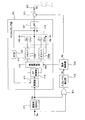
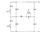
- FIG. 1 is a block diagram illustrating a configuration of an output stage of the digital amplifier according to the first embodiment.
- the digital amplifier according to the first embodiment includes a digital amplifier unit 101, an input level detection unit 103, and an operation control unit 105. Note that a load such as a speaker is connected to the output terminal 107 provided in the subsequent stage of the digital amplifier unit 101.
- the digital amplifier unit 101 amplifies the input signal.
- the signal input to the digital amplifier unit 101 is an audio signal, for example, and the format may be analog or digital.
- the digital amplifier unit 101 includes a modulation unit 111, a dead time control unit (DT control unit) 113, an oscillation control unit 115, a drive unit 117, a switching unit 119, an LPF (Low ⁇ Pass). Filter) 121 and NFB (Negative FeedBack) 123.
- the modulation unit 111 is a PWM (PulsePWidth Modulation) circuit, for example, and converts the signal input to the digital amplifier unit 101 into a digital pulse signal.
- the modulation unit 111 outputs a digital pulse signal corrected according to the feedback signal from the NFB 123.
- the switching unit 119 includes switching elements 131a and 131b connected in series in two upper and lower stages, and amplifies signals by switching.
- the switching elements 131a and 131b are power transistors, MOSFETs, or IGBTs.
- the drive unit 117 includes drivers 133a and 133b configured in two upper and lower stages.
- the driver 133a performs switching driving of the switching element 131a
- the driver 133b performs switching driving of the switching element 131b.
- the drivers of the driving unit 117 drive the switching elements 131a and 131b so that the switching elements 131a and 131b ideally operate in reverse logic.
- the on / off state of the actual transistor element is switched, there is a turn-on time or a turn-off time. For this reason, an upper and lower short circuit in which both of the switching elements 131a and 131b are turned on occurs. In order to prevent this state, it is only necessary to set a time during which both switching elements are turned off, that is, a “dead time” at a timing when one of the switching elements is switched from the off state to the on state.
- the dead time control unit (DT control unit) 113 controls the drive unit 117 so as to provide a dead time when the switching unit 119 performs switching. Note that if the dead time is long, the duty ratio of the signals input to the switching elements 131a and 131b becomes small, so there is no need to provide a separate duty ratio adjustment circuit.
- the oscillation control unit 115 can select start and stop of oscillation. Specifically, it is selected whether the digital pulse signal applied from the dead time control unit 113 is transmitted to the driver or not.
- the oscillation control unit 115 oscillates according to the potential of the output signal of the operation control unit 105, and opens and closes the path.
- the LPF 121 is a demodulating means composed of an LC circuit.
- the LPF 121 filters the mid-high frequency band, so that the digital pulse signal amplified by the switching unit 119 is demodulated.
- the demodulated signal is output from the output terminal 107.
- the NFB 123 is a negative feedback amplifier circuit, and feeds back the output signal of the switching unit 119 to the modulation unit 111.
- the input level detection unit 103 detects the presence or absence of an input signal by detecting the level of the input signal.
- the input level detection unit 103 outputs a signal obtained by performing both-wave rectification on the input signal.
- the input signal is an audio signal, for example, and the format may be analog or digital. Further, the input level detection unit 103 may perform single-wave rectification, AC-DC conversion, sample hold, AC level detection, or the like instead of double-wave rectification.
- the operation control unit 105 controls the oscillation operation by the oscillation control unit 115 of the digital amplifier unit 101 in accordance with the signal input from the input level detection unit 103. By this control, the start or stop of the switching operation performed by the switching unit 119 is controlled. Note that the level of the input signal at which the switching operation is actually started or stopped is equal to or higher than the residual noise of the digital amplifier of this embodiment, and is about ⁇ 60 dBm to ⁇ 40 dBm.
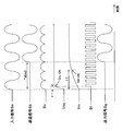
- FIG. 2 is a diagram showing signal waveforms when a switching operation is started in the digital amplifier according to the first embodiment.
- FIG. 3 is a diagram illustrating signal waveforms when the switching operation is stopped in the digital amplifier according to the first embodiment.
- the signal Sa shown in FIGS. 2 and 3 is an input signal of the digital amplifier.
- the signal Sc is an output signal of the input level detection unit 103 and is a signal obtained by performing both-wave rectification on the input signal Sa.
- the potential Voc is a potential of the output signal of the operation control unit 105 and is a signal obtained by smoothing the signal Sc.
- the signal Sf is a signal indicating a switching operation performed by the switching unit 119 of the digital amplifier unit 101.
- the signal Sg is a signal obtained by amplifying the input signal Sa and is an output signal of the digital amplifier.
- the signal Sg is output from the output terminal 107.
- the state where the input signal Sa is approximately 0 V potential that is, the state where there is no input signal Sa (no signal input state)
- the state where there is some level that is, the state where the input signal Sa is present (signal input).
- Change to (state) the potential Voc of the output signal of the operation control unit 105 increases.
- the oscillation control unit 115 transmits the digital pulse signal applied from the dead time control unit 113 to the drive unit 117.
- the oscillation control unit 115 includes a photocoupler and an electronic switch.
- the oscillation control unit 115 is configured to open and close the current flowing into the input of the photocoupler with an electronic switch such as a transistor, and transmits the digital pulse signal by closing the electronic switch and flowing the current.
- the drive part 117 starts the drive control of the switching part 119 according to the input signal Sa.
- the switching operation is started, and the signal Sg is output from the output terminal 107.
- the output terminal 107 does not output a signal corresponding to the signal Sa until the switching operation is started. That is, the “sound lack” indicated by the one-dot chain line in FIG. 2 occurs.
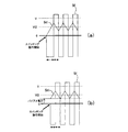
- pop noise Pop Noise due to the resonance phenomenon of the LPF 121 occurs.
- the timing at which the switching operation is stopped has no correlation with the input signal Sa, and the position of the signal Sf output from the switching unit 119 is unknown.
- a pop noise component is generated in the LPF 121, and unnecessary pop noise is output from the speaker.
- the switching operation in the digital amplifier unit 101 is started or stopped according to the presence or absence of the signal Sa input to the digital amplifier. That is, the switching operation is performed in the signal input state, and the switching operation is not performed in the no-signal input state. Therefore, power consumption in the digital amplifier unit 101 when no signal is input can be reduced.
- FIG. 4 is a block diagram illustrating a configuration of an output stage of the digital amplifier according to the second embodiment.
- the digital amplifier according to the second embodiment further includes a delay unit 211 in front of the digital amplifier unit 101 in addition to the components of the digital amplifier according to the first embodiment. Except for this point, the second embodiment is the same as the first embodiment.
- the same reference numerals are given to the same components as those in FIG. 1.
- the delay unit 211 delays transmission of the signal for a predetermined time when transmitting the signal input to the digital amplifier to the subsequent component. Therefore, the signal input to the digital amplifier is input to the digital amplifier unit 101 with a delay of this time. Note that the delay time set in the delay unit 211 can be arbitrarily set. Further, the signal input to the input level detection unit 103 is the input signal Sa as in the first embodiment.
- FIG. 5 is a diagram showing signal waveforms when the switching operation is started in the digital amplifier according to the second embodiment.
- FIG. 6 is a diagram illustrating signal waveforms when the switching operation is stopped in the digital amplifier according to the second embodiment.
- the signal Sa shown in FIGS. 5 and 6 is an input signal of the digital amplifier.
- the signal Sb is an output signal (delay signal) of the delay unit 211 and is input to the digital amplifier unit 101.
- the signal Sc is an output signal of the input level detection unit 103 and is a signal obtained by performing both-wave rectification on the input signal Sa.
- the potential Voc is a potential of the output signal of the operation control unit 105 and is a signal obtained by smoothing the signal Sc.
- the signal Sf is a signal indicating a switching operation performed by the switching unit 119 of the digital amplifier unit 101.
- the signal Sg is an amplified signal of the signal Sb and is an output signal of the digital amplifier.
- the signal Sg is output from the output terminal 107.
- the switching operation in the digital amplifier unit 101 is started or stopped in accordance with the presence or absence of the signal Sa input to the digital amplifier.
- the power consumption at 101 can be reduced. Furthermore, since the signal Sb input to the digital amplifier unit 101 is delayed, no sound loss occurs when the digital amplifier unit 101 starts a switching operation.
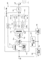
- FIG. 7 is a block diagram illustrating a configuration of an output stage of the digital amplifier according to the third embodiment.
- the digital amplifier according to the third embodiment further includes a switch 311 at the subsequent stage of the digital amplifier unit 101 in addition to the components of the digital amplifier according to the second embodiment.
- the operation control unit 305 of the present embodiment is different from the operation control unit 105 of the second embodiment in that the switch 311 is further on / off controlled. Except for these points, the second embodiment is the same as the second embodiment.
- the same reference numerals are given to the same components as those in FIG. 4.
- the switch 311 is a relay provided on a path through which the output signal of the digital amplifier unit 101 is output from the output terminal 107, and opens and closes the path.
- the switch 311 is an electronic relay such as a mechanical relay or a photo MOS relay, and is controlled by the operation control unit 305.
- the operation control unit 305 according to the present embodiment controls not only the oscillation operation of the oscillation control unit 115 but also the opening / closing of the switch 311 according to the signal output from the input level detection unit 103.
- the operation control unit 305 has time constants at the time of rising and falling of the potential of the signal output to the oscillation control unit 115, and time constants at the time of rising and falling of the potential of the signal output to the switch 311. Includes a time constant circuit for setting
- the timing at which the switch 311 is switched from the open state to the closed state by the control of the operation control unit 305 is the start timing of the switching operation in the digital amplifier unit 101 by the control of the operation control unit 305.
- the timing at which the switch 311 is closed is less than the delay time td.
- the time constant at the time of falling of the potential of the signal output from the operation control unit 305 to the switch 311 is larger than the time constant at the time of falling of the potential of the signal output from the operation control unit 305 to the oscillation control unit 115. small. Therefore, when the digital amplifier receives no signal, the timing at which the switch 311 is switched from the closed state to the open state under the control of the operation control unit 305 is higher than the stop timing of the switching operation in the digital amplifier unit 101 under the control of the operation control unit 305. It is before.
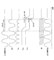
- FIG. 8 is a diagram showing signal waveforms when a switching operation is started in the digital amplifier according to the third embodiment.
- FIG. 9 is a diagram illustrating signal waveforms when the switching operation is stopped in the digital amplifier according to the third embodiment.
- the signal Sa shown in FIGS. 8 and 9 is an input signal of the digital amplifier.
- the signal Sb is an output signal (delay signal) of the delay unit 211 and is input to the digital amplifier unit 101. 8 and 9, there is a difference in delay time td [msec] on the time axis between the input signal Sa and the delay signal Sb.
- the signal Sc is an output signal of the input level detection unit 103 and is a signal obtained by performing both-wave rectification on the input signal Sa.
- the potential Voc is a signal potential output from the operation control unit 305 to the oscillation control unit 115, and is a signal obtained by smoothing the signal Sc.
- the potential Vrs is a signal potential output from the operation control unit 305 to the switch 311 and is a signal obtained by smoothing the signal Sc.
- the signal Sf is a signal indicating a switching operation performed by the switching unit 119 of the digital amplifier unit 101.
- the signal Sg is an amplified signal of the signal Sb and is an output signal of the digital amplifier.
- the signal Sg is output from the output terminal 107.
- the switching operation is started.
- the switch 311 is changed from the open state to the closed state by increasing the potential Vrs (SW ON).
- the time constant ⁇ 2 is larger than the time constant ⁇ 1. For this reason, the timing when the switch 311 is closed is within the delay time td as shown in FIG. 8, but after the timing when the switching operation is started.
- the switch 311 is closed, the signal Sg is output from the output terminal 107.
- the drive unit 117 stops the drive control of the switching unit 119. In this way, the switching operation is stopped.
- the time constant ⁇ 4 is smaller than the time constant ⁇ 3. For this reason, the timing at which the switch 311 is opened is earlier than the timing at which the switching operation is stopped, as shown in FIG. However, as shown in FIG. 9, since the switch 311 is opened while the signal Sg is being output from the output terminal 107, “sound break” indicated by a one-dot chain line in FIG. 9 occurs.
- the switching operation in the digital amplifier unit 101 is started or stopped in accordance with the presence or absence of the signal Sa input to the digital amplifier.
- the power consumption at 101 can be reduced.
- the signal Sb input to the digital amplifier unit 101 is delayed, no sound loss occurs when the digital amplifier unit 101 starts a switching operation.
- the switch 311 is controlled to open and close so that the switch 311 is in an open state during the time when the pop noise can occur, the pop noise is not output from the output terminal 107.
- FIG. 10 is a block diagram illustrating a configuration of an output stage of the digital amplifier according to the fourth embodiment.
- the digital amplifier according to the fourth embodiment further includes an OR circuit 411 in front of the input level detection unit 103 in addition to the components of the digital amplifier according to the third embodiment.
- the input level detection unit 403 of the present embodiment is different from the input level detection unit 103 of the third embodiment in that an output signal from the OR circuit 411 is input. Except for these points, the third embodiment is the same as the third embodiment.
- the same reference numerals are given to the same components as those in FIG. 7.
- the OR circuit 411 In the OR circuit 411, the signal Sa input to the digital amplifier and the output signal Sb of the delay unit 211 are input.
- the OR circuit 411 outputs a logical sum signal of the signal Sa input to the digital amplifier and the output signal Sb of the delay unit 211.
- the logical sum signal is a signal obtained by superimposing the output signal Sb of the delay unit 211 on the signal Sa input to the digital amplifier.
- the input level detection unit 403 controls the oscillation operation by the oscillation control unit 115 of the digital amplifier unit 101 in accordance with the logical sum signal output from the OR circuit 411.
- FIG. 11 is a diagram showing signal waveforms when a switching operation is started in the digital amplifier according to the fourth embodiment.
- FIG. 12 is a diagram illustrating signal waveforms when the switching operation is stopped in the digital amplifier according to the fourth embodiment.
- a signal Sa shown in FIGS. 11 and 12 is an input signal of the digital amplifier.
- the signal Sb is an output signal (delay signal) of the delay unit 211 and is input to the digital amplifier unit 101.
- delay time td [msec]
- the signal Sc is an output signal of the input level detection unit 403 and is a signal obtained by superimposing a signal obtained by performing both-wave rectification on the input signal Sa and a signal obtained by performing both-wave rectification on the delayed signal Sb.
- the potential Voc is a signal potential output from the operation control unit 105 to the oscillation control unit 115, and is a signal obtained by smoothing the signal Sc.
- the potential Vrs is a signal potential output from the operation control unit 105 to the switch 311 and is a signal obtained by smoothing the signal Sc.
- the signal Sf is a signal indicating a switching operation performed by the switching unit 119 of the digital amplifier unit 101.
- the signal Sg is an amplified signal of the signal Sb and is an output signal of the digital amplifier.
- the signal Sg is output from the output terminal 107.
- the switching operation is started.
- the switch 311 is changed from the open state to the closed state by increasing the potential Vrs (SW ON).
- the time constant ⁇ 2 is larger than the time constant ⁇ 1. For this reason, the timing when the switch 311 is closed is within the delay time td as shown in FIG. 11, but after the timing when the switching operation is started.
- the switch 311 is closed, the signal Sg is output from the output terminal 107.
- the switching operation in the digital amplifier unit 101 is started or stopped in accordance with the presence or absence of the signal Sa input to the digital amplifier.
- the power consumption at 101 can be reduced.
- the signal Sb input to the digital amplifier unit 101 is delayed, no sound loss occurs when the digital amplifier unit 101 starts a switching operation.
- the switch 311 is controlled to open and close so that the switch 311 is in an open state during the time when the pop noise can occur, the pop noise is not output from the output terminal 107.
- the switch 311 does not open until at least the delay time has elapsed after the input signal Sa disappears, so that no sound interruption occurs.
- FIG. 13 is a block diagram illustrating a configuration of an output stage of the digital amplifier according to the fifth embodiment.
- the digital amplifier according to the fifth embodiment further includes an operation sequence setting unit 125 in addition to the components of the digital amplifier according to the first embodiment.
- the operation sequence setting unit 125 receives the signal Sc output from the input level detection unit 103.
- the digital amplifier unit 101 of this embodiment further includes a gain correction unit 511 between the modulation unit 111 and the DT control unit 113. Except for these points, the second embodiment is the same as the first embodiment.
- the same reference numerals are given to the same components as those in FIG. 1.
- the time from the start of oscillation of the oscillation control unit 115 to the time when the output of the switching unit 119 reaches the modulation unit 111 via the NFB 123 is not subjected to negative feedback by the NFB 123, so the reproducibility as a digital amplifier is reduced.
- the decrease in reproducibility is specifically distortion of the output signal of the digital amplifier due to a decrease in power supply voltage supplied to the digital amplifier.
- the gain correction unit 511 performs correction to increase the gain of the digital amplifier unit 101 in order to compensate for a decrease in reproducibility. Note that the gain correction amount by the gain correction unit 511 is variable and can be set by the operation sequence setting unit 125. When a signal is input to the digital amplifier, the operation sequence setting unit 125 drives the gain correction unit 511 for a predetermined time immediately after the signal is input.
- the gain correction unit 511 corrects the gain of the digital amplifier unit 101 for a predetermined time immediately after the signal is input to the digital amplifier. Therefore, it is possible to compensate for a decrease in signal reproducibility immediately after the oscillation control unit 115 starts oscillation.
- the gain correction unit 511 is disposed on the rear stage side of the modulation unit 111, but may be disposed on the front stage of the modulation unit 111. Even in this case, a reduction in reproducibility can be compensated.
- FIG. 14 is a block diagram illustrating a configuration of an output stage of the digital amplifier according to the sixth embodiment.
- the digital amplifier according to the sixth embodiment further includes a power supply voltage detection unit 611 in the digital amplifier unit 101 in addition to the components of the digital amplifier according to the fifth embodiment.
- the gain correction unit 613 of this embodiment is different from the gain correction unit 511 of the fifth embodiment in that an output signal from the power supply voltage detection unit 611 is input. Except for these points, this embodiment is the same as the fifth embodiment.
- the same reference numerals are assigned to components common to FIG. 13.
- the power supply voltage detection unit 611 detects the power supply voltage Vb and sends a signal indicating the detection result to the gain correction unit 613.
- the gain correction unit 613 of this embodiment corrects the gain of the digital amplifier unit 101 according to the power supply voltage Vb indicated by the signal sent from the power supply voltage detection unit 611. For example, when the actual value of the power supply voltage Vb is lower than a specified value, the gain of the digital amplifier unit 101 decreases. Therefore, the gain correction unit 613 performs gain correction corresponding to the decrease from the desired value of the power supply voltage Vb.
- the operation sequence setting unit 125 in addition to setting the gain correction amount by the operation sequence setting unit 125, it is possible to correct the gain according to the change in the power supply voltage Vb. Therefore, the accuracy is higher than that of the fifth embodiment. Gain correction is possible.
- FIG. 15 is a block diagram illustrating a configuration of an output stage of the digital amplifier according to the seventh embodiment.
- the digital amplifier according to the seventh embodiment further includes an NFB amount control unit 151 subsequent to the input level detection unit 103 in addition to the components of the digital amplifier according to the first embodiment. Note that the signal Sc output from the input level detection unit 103 is input to the NFB amount control unit 151. Except for this point, the second embodiment is the same as the first embodiment. In FIG. 15, the same reference numerals are given to the components common to FIG. 1.
- the NFB amount control unit 151 controls the feedback amount to the modulation unit 111 by the NFB 123.
- the order of the NFB 123 is variable, and in order to ensure the reproducibility of a high-frequency signal near 20 kHz input to the digital amplifier unit 101, a secondary or higher-order low-pass filter with good attenuation characteristics is usually formed. . Note that the higher the order of the NFB 123, the greater the amount of NFB.
- the secondary or higher order NFB has a slower tracking speed with respect to the switching waveform of the input signal Sf than the primary NFB with a small amount of NFB. For this reason, immediately after the switching unit 119 starts the switching operation, NFB is not applied and reproducibility as a digital amplifier is low. Therefore, when a signal is input to the digital amplifier, the NFB amount control unit 151 controls the NFB 123 so that the order of the NFB 123 is reduced to the first order for a predetermined time immediately after the signal is input. Therefore, it is possible to avoid a decrease in signal reproducibility immediately after the oscillation controller 115 starts oscillation.
- FIG. 16 is a block diagram illustrating a configuration of an output stage of the digital amplifier according to the eighth embodiment.
- the digital amplifier according to the eighth embodiment further includes an operation sequence setting unit 127 in addition to the components of the digital amplifier according to the first embodiment.
- the operation sequence setting unit 127 receives the signal Sc output from the input level detection unit 103.
- the digital amplifier unit 101 of this embodiment further includes an output switching unit 711 between the modulation unit 111 and the DT control unit 113, and a non-feedback modulation unit 713 in parallel with the modulation unit 111. Except for these points, the second embodiment is the same as the first embodiment.
- the same reference numerals are given to the same components as those in FIG. 1.
- the non-feedback modulation unit 713 is, for example, a PWM (Pulse Width Modulation) circuit, and converts a signal input to the digital amplifier unit 101 into a digital pulse signal. Note that, unlike the modulation unit 111, no feedback signal from the NFB 123 is input to the non-feedback modulation unit 713. Therefore, the non-feedback modulation unit 713 does not perform correction according to the feedback signal.
- the output switching unit 711 switches the signal output to the DT control unit 113 to either the digital pulse signal converted by the modulation unit 111 or the digital pulse signal converted by the non-feedback modulation unit 713.
- the operation sequence setting unit 127 sets the output switching unit 711 so that the output switching unit 711 outputs the signal from the non-feedback modulation unit 713 for a predetermined time immediately after the signal is input. Control.
- the modulation unit 111 when the modulation unit 111 is configured with a low slew rate operational amplifier, when the PWM carrier (approximately 200 kHz to 500 kHz) output from the switching unit 119 is directly applied to the modulation unit 111, the PWM carrier The linearity of the operational amplifier is reduced and the reproducibility is reduced.
- the PWM carrier approximately 200 kHz to 500 kHz
- the signal from the non-feedback modulation unit 713 is used for a predetermined time immediately after the signal is input to the digital amplifier. Since the non-feedback modulation unit 713 does not originally perform correction using the feedback signal, it is not affected by the presence or absence of the feedback signal from the NFB 123. Therefore, it is possible to avoid a decrease in signal reproducibility immediately after the oscillation controller 115 starts oscillation.
- the output switching unit 711 switches to either the signal from the modulation unit 111 or the signal from the non-feedback modulation unit 713, but a signal that is synthesized by gradually changing the ratio of these two signals. May be output.
- FIG. 17 is a block diagram illustrating a configuration of an output stage of the digital amplifier according to the ninth embodiment.
- the digital amplifier according to the ninth embodiment includes a non-feedback modulation unit 713 and an output switching unit 711 in the digital amplifier unit 101 in addition to the components of the digital amplifier according to the eighth embodiment.
- a gain correction unit 811 is further included. Except for this point, this embodiment is the same as the eighth embodiment.
- FIG. 17 the same reference numerals are given to components common to FIG. 16.
- the operation sequence setting unit 127 drives the gain correction unit 811 for a predetermined time immediately after the signal is input.
- the digital pulse signal from the non-feedback modulation unit 713 is output to the gain correction unit 811.
- the gain correction unit 811 corrects the gain of the digital amplifier unit 101 in order to compensate for a decrease in reproducibility.
- the signal from the non-feedback modulation unit 713 is used for a predetermined time immediately after the signal is input to the digital amplifier, and the gain correction unit 811 corrects the gain of the digital amplifier unit 101. To do. For this reason, the gain correction unit 811 corrects the gain of the digital amplifier unit 101 even when the use of the non-feedback modulation unit 713 cannot completely avoid a decrease in signal reproducibility immediately after the oscillation control unit 115 starts oscillation. For this reason, it is possible to better compensate for a decrease in signal reproducibility immediately after the oscillation controller 115 starts oscillation.
- FIG. 18 is a block diagram illustrating a configuration of an output stage of the digital amplifier according to the tenth embodiment.
- the digital amplifier according to the tenth embodiment further includes a power supply voltage detection unit 911 in the digital amplifier unit 101 in addition to the components of the digital amplifier according to the ninth embodiment. Except for this point, the present embodiment is the same as the ninth embodiment.
- the same reference numerals are assigned to components common to FIG.
- the power supply voltage detection unit 911 detects the power supply voltage Vb and sends a signal indicating the detection result to the gain correction unit 811.
- the operation sequence setting unit 127 drives the gain correction unit 811 for a predetermined time immediately after the signal is input.
- the gain correction unit 811 of this embodiment corrects the gain of the digital amplifier unit 101 according to the power supply voltage Vb indicated by the signal sent from the power supply voltage detection unit 911. For example, when the actual value of the power supply voltage Vb is lower than a specified value, the gain of the digital amplifier unit 101 decreases. Therefore, the gain correction unit 811 performs gain correction corresponding to the decrease from the desired value of the power supply voltage Vb.
- the gain can be corrected according to the change in the power supply voltage Vb.
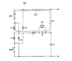
- FIG. 19 is a block diagram illustrating a configuration of an output stage of the digital amplifier according to the eleventh embodiment.
- the digital amplifier according to the eleventh embodiment further includes an operation sequence setting unit 153 in addition to the components of the digital amplifier according to the first embodiment.
- the operation sequence setting unit 153 receives the signal Sc output from the input level detection unit 103.
- the digital amplifier unit 101 of the present embodiment includes a secondary ⁇ modulator 161, a primary ⁇ modulator 163, and an output switching unit 165 instead of the modulator 111, and the path of the NFB 123 is a secondary ⁇ modulator. 161 and the first-order ⁇ modulator 163.
- the second embodiment is the same as the first embodiment.
- the same reference numerals are given to the same components as those in FIG. 1.
- the signal Sa is input to the secondary ⁇ modulation unit 161 and the primary ⁇ modulation unit 163, respectively.
- the output signals of the secondary ⁇ modulator 161 and the primary ⁇ modulator 163 are input to the output switching unit 165.
- the output switching unit 165 switches the output signal from the secondary ⁇ modulation unit 161 or the output signal from the primary ⁇ modulation unit 163 as a signal to be output to the DT control unit 113.
- the output signal Sf of the switching unit 119 is applied to the primary ⁇ modulation unit 163 and the secondary ⁇ modulation unit 161 via the NFB 123. Since the primary ⁇ modulation unit 163 has better followability to the signal Sf than the secondary ⁇ modulation unit 161, the reproducibility immediately after the oscillation control unit 115 starts oscillation is good. The decrease in reproducibility is a distortion of an audio signal caused by a decrease in power supply voltage supplied to the digital amplifier. Further, the secondary ⁇ modulation unit 161 can increase the amount of NFB compared to the primary ⁇ modulation unit 163, and the reproducibility is not good until a sufficient time has elapsed from the oscillation of the oscillation control unit 115.
- the output switching unit 165 outputs a signal from the primary ⁇ modulation unit 163 for a predetermined time immediately after the oscillation of the oscillation control unit 115, and outputs a signal from the secondary ⁇ modulation unit 161 after the predetermined time has elapsed. Output.
- the output signal from the primary ⁇ modulator 163 with good reproducibility is used immediately after the oscillation control unit 115 starts oscillation, and the output signal of the secondary ⁇ modulator 161 is used after a sufficient time has elapsed. It is done. For this reason, it is possible to avoid a decrease in signal reproducibility immediately after the oscillation controller 115 starts oscillation. Note that the same effect can be obtained when the order of the ⁇ modulation unit is higher than the order immediately after the start of oscillation if the order after sufficient time has elapsed. Further, if the ⁇ modulator is a 1-bit digital pulse converter such as a ⁇ modulator, the same effect can be obtained.
- the output switching unit 165 switches between the signal from the secondary ⁇ modulation unit 161 and the signal from the primary ⁇ modulation unit 163, but gradually changes the ratio of these two signals.
- the synthesized signal may be output.
- FIG. 20 is a block diagram illustrating a configuration of an output stage of the digital amplifier according to the twelfth embodiment.
- the digital amplifier according to the twelfth embodiment further includes an operation sequence setting unit 171 in addition to the components of the digital amplifier according to the first embodiment.
- the operation sequence setting unit 171 receives the signal Sc output from the input level detection unit 103.
- the second embodiment is the same as the first embodiment.
- the same reference numerals are given to components common to FIG. 1.
- the operation sequence setting unit 171 controls the DT control unit 113 so that the switching unit 119 performs the switching operation with a dead time longer than normal for a predetermined time after the switching unit 119 of the digital amplifier unit 101 starts the switching operation. To do.
- FIG. 21 is a diagram showing signal waveforms when the switching operation is started in the digital amplifier according to the twelfth embodiment.
- a signal Sa shown in FIG. 21 is an input signal of the digital amplifier.
- the signal Sc is an output signal of the input level detection unit 103 and is a signal obtained by performing both-wave rectification on the input signal Sa.
- the potential Voc is a potential of the output signal of the operation control unit 105 and is a signal obtained by smoothing the signal Sc.
- the signal Sf is a signal indicating a switching operation performed by the switching unit 119 of the digital amplifier unit 101.
- the signal Sg is a signal obtained by amplifying the signal Sa and is an output signal of the digital amplifier.
- the signal Sg is output from the output terminal 107.
- the driving unit 117 has a configuration in which a photocoupler is incorporated, signal transmission is performed by the photocoupler, and current flowing into the input of the photocoupler is opened and closed by an electronic switch such as a transistor. Indicates that the electronic switch is closed and a signal is transmitted.
- the drive part 117 starts the drive control of the switching part 119 according to the input signal Sa.
- the operation sequence setting unit 171 controls the DT control unit 113 to perform the switching operation with a dead time longer than normal for a predetermined time Tld [msec] after the switching unit 119 starts the switching operation.
- the duty ratio of the signals input to the drivers 133a and 133b is shortened.
- the duty ratio is short, the amount of information of the input signal Sa in the signal modulated by the modulation unit 111 decreases, and distortion of the output signal Sg occurs when demodulated by the LPF 121, so that the signal reproducibility deteriorates. To do. Therefore, it is preferable that the predetermined time Tld during which the DT control unit 113 performs control with a dead time longer than usual is shorter.
- the noise generated during the dead time is not output from the output terminal 107.
- the on-time of the switching elements 131a and 131b is shortened, the average current value flowing through the LPF 121 is suppressed, and the pop caused by the resonance phenomenon of the LPF 121 is caused. Noise can be reduced. For example, if the control of this embodiment is not performed, pop noise indicated by a one-dot chain line in FIG. 21 is generated, but in this embodiment, the pop noise is small as indicated by a solid line.
- FIG. 22 is a block diagram illustrating a configuration of an output stage of the digital amplifier according to the thirteenth embodiment.
- the digital amplifier according to the thirteenth embodiment further includes an operation sequence setting unit 171 in addition to the components of the digital amplifier according to the second embodiment.
- the operation sequence setting unit 171 receives the signal Sc output from the input level detection unit 103.
- the second embodiment is the same as the second embodiment.
- the same reference numerals are given to the same components as those in FIG. 4.
- the operation sequence setting unit 171 controls the DT control unit 113 so that the switching unit 119 performs the switching operation with a dead time longer than normal for a predetermined time after the switching unit 119 of the digital amplifier unit 101 starts the switching operation. To do.
- FIG. 23 is a diagram showing signal waveforms when the switching operation is started in the digital amplifier according to the thirteenth embodiment.
- a signal Sa shown in FIG. 23 is an input signal of the digital amplifier.
- the signal Sb is an output signal (delay signal) of the delay unit 211 and is input to the digital amplifier unit 101.
- the signal Sc is an output signal of the input level detection unit 103 and is a signal obtained by performing both-wave rectification on the input signal Sa.
- the potential Voc is a potential of the output signal of the operation control unit 105 and is a signal obtained by smoothing the signal Sc.
- the signal Sf is a signal indicating a switching operation performed by the switching unit 119 of the digital amplifier unit 101.
- the signal Sg is a signal obtained by amplifying the delay signal Sb and is an output signal of the digital amplifier.
- the signal Sg is output from the output terminal 107.
- the driving unit 117 has a configuration in which a photocoupler is incorporated, signal transmission is performed by the photocoupler, and current flowing into the input of the photocoupler is opened and closed by an electronic switch such as a transistor. Indicates that the electronic switch is closed and a signal is transmitted.
- the drive part 117 starts the drive control of the switching part 119 according to the delay signal Sb.
- the operation sequence setting unit 171 controls the DT control unit 113 to perform the switching operation with a dead time longer than normal for a predetermined time Tld [msec] after the switching unit 119 starts the switching operation.
- the duty ratio of the signals input to the drivers 133a and 133b is shortened.
- the duty ratio is short, the amount of information of the input signal Sa in the signal modulated by the modulation unit 111 decreases, and distortion of the output signal Sg occurs when demodulated by the LPF 121, so that the signal reproducibility deteriorates. To do. Therefore, it is preferable that the predetermined time Tld during which the DT control unit 113 performs control with a dead time longer than usual is shorter.
- the noise generated during the dead time is not output from the output terminal 107.
- the on-time of the switching elements 133a and 133b is shortened, the average current value flowing through the LPF 121 is suppressed, and the pop caused by the resonance phenomenon of the LPF 121 is caused. Noise can be reduced. For example, if the control of the present embodiment is not performed, pop noise indicated by a one-dot chain line in FIG. 23 is generated, but in this embodiment, the pop noise is small as indicated by a solid line.
- the output signal Sg lacks sound.
- the signal Sb input to the digital amplifier unit 101 is delayed, no sound loss occurs when the digital amplifier unit 101 starts a switching operation.
- FIG. 24 is a block diagram illustrating a configuration of an output stage of the digital amplifier according to the fourteenth embodiment.
- the digital amplifier of the fourteenth embodiment includes an initial waveform adder 1111 and an initial stage in front of the modulator 111 in the digital amplifier 101.
- An operation sequence setting unit 125 that controls the waveform adding unit 1111 is further included. Except for this point, the second embodiment is the same as the first embodiment. In FIG. 24, the same reference numerals are given to the components common to FIG. 1.
- the operation sequence setting unit 125 receives the signal detected by the input level detection unit 103 from the no-signal state to the signal input state, and controls the initial waveform addition unit 1111 for a certain period sufficient to suppress pop noise. .
- the initial waveform adding unit 1111 adds a signal having the same amplitude and opposite phase as the pop noise generated when the switching operation is started to the signal input to the digital amplifier unit 101.
- the initial waveform adder 1111 may be provided at the subsequent stage of the modulator 111. In this case, the initial waveform addition unit 1111 adds a signal having the same amplitude and opposite phase as the pop noise modulation signal to the digital pulse signal output from the modulation unit 111.
- the signal is added before the amplification by the signal added by the initial waveform adding unit 1111.
- Pop noise is not output.
- the pop noise is, for example, pop noise caused by the resonance phenomenon of the LPF 121 or pop noise caused by a difference between an operation reference point of the modulation unit 111 and an operation reference point of the switching unit 119 described later.
- FIG. 25 is a block diagram illustrating a configuration of an output stage of the digital amplifier according to the fifteenth embodiment.
- the digital amplifier according to the fifteenth embodiment further includes a stop position detector 1211 in addition to the components of the digital amplifier according to the first embodiment.
- the operation control unit 1205 of this embodiment is different from the operation control unit 105 of the first embodiment in the timing at which the digital amplifier unit 101 stops the switching operation. Except for these points, the second embodiment is the same as the first embodiment.
- the same reference numerals are given to the same components as those in FIG.
- the stop position detection unit 1211 detects a position where the output voltage or output current value of the switching unit 119 becomes 0, sends a signal indicating the detection result to the operation control unit 1205, and controls the oscillation operation by the oscillation control unit 115. To do. Thereby, the switching operation can be stopped at a position where the value of the output voltage or output current becomes zero.
- a low resistance is inserted in the current path and converted into a voltage to detect the value.
- the switching operation is performed at a position where the output voltage or output current value of the switching unit 119 becomes 0 (position where the power becomes 0). Is stopped. For this reason, it is possible to reduce pop noise that occurs when the digital amplifier enters a no-signal input state.
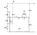
- FIG. 27 is a block diagram illustrating a configuration of an output stage of the digital amplifier according to the sixteenth embodiment.
- the digital amplifier according to the sixteenth embodiment further includes an operation sequence setting unit 133 in addition to the components of the digital amplifier according to the first embodiment, and an output voltage detection unit within the digital amplifier unit 101. 1311 and an initial voltage adjustment unit 1313. Except for these points, the second embodiment is the same as the first embodiment.
- the same reference numerals are given to the same components as those in FIG.
- an integrator such as a high-speed operational amplifier IC is configured on the input side of the modulation unit 111 constituting the digital amplifier.
- the integrator is driven by a single power source whose power source voltage is +5 [V] or the like.
- the switching unit 119 is driven by a dual power source having a power source voltage of ⁇ 20 [V].
- both the input signal and the output signal need to be alternating current. Therefore, +2.5 [V] which is half of +5 [V] is driven as an operation reference point for the integrator, and 0 [V] which is an intermediate value of ⁇ 20 [V] for the switching unit 119.
- a level shift circuit such as a photocoupler is built in the driving unit 117 so that the operation reference point is matched.
- the output voltage of the digital amplifier in the no-signal input state is almost 0 [V] because the switching unit 119 has high impedance and the load impedance is 4 to 8 [ ⁇ ].
- the integrator of the modulation unit 111 is driven at the operation reference point of +2.5 [V] by the bias voltage of the negative terminal of the operational amplifier constituting the integrator.
- the input voltage of the integrator in the no-signal input state is 0 [V]
- the output voltage is +2.5 [V] which is the operation reference point. That is, the integrator in the no-signal input state stands by with +2.5 [V] applied to the capacitor constituting the integrator.
- the output voltage detection unit 1311 detects the voltage on the output side of the switching unit 119 and sends a signal indicating the detection result to the initial voltage adjustment unit 1313.
- the initial voltage adjustment unit 1313 adjusts the voltage on the output side of the modulation unit 111 to be equal to the voltage indicated by the signal sent from the output voltage detection unit 1311. That is, the initial voltage adjustment unit 1313 applies a predetermined bias voltage to the integrator of the modulation unit 111.
- the operation sequence setting unit 133 drives the initial voltage adjustment unit 1313 for a predetermined time immediately after the signal is input.
- FIG. 28 is a diagram illustrating a waveform of the output voltage Sd of the modulation unit and a waveform of the output voltage Sf of the switching unit when the digital amplifier unit starts a switching operation.
- FIG. 28A illustrates a bias voltage applied to the modulation unit. The waveform when not biased is shown, and (b) shows the waveform when a bias voltage is applied to the modulation section.
- FIG. 28A when the configuration is not the configuration of the sixteenth embodiment, when the signal input state is changed from the no-signal input state and the switching operation is started, +2.5 in the integrator of the modulation unit 111 is started. The potential difference of [V] affects the switching cycle, and the duty ratio of the output voltage Sf of the switching unit 119 does not become 50%. As a result, pop noise occurs.
- a bias voltage is applied to the integrator of the modulation unit 111 so that the voltage on the output side of the modulation unit 111 matches the voltage on the output side of the switching unit 119. Therefore, pop noise does not occur when the digital amplifier unit 101 starts a switching operation.
- the switching unit 119 included in the digital amplifier unit 101 of the embodiment described above includes two switching elements, but may be one or four. Note that the number of drivers included in the drive unit 117 corresponds to the number of switching elements included in the switching unit 119.
- At least one of the fifth to sixteenth embodiments may be combined with any of the first to fourth embodiments.
- the present invention is useful as a digital amplifier that does not perform a switching operation when no signal is input.
Landscapes
- Engineering & Computer Science (AREA)
- Power Engineering (AREA)
- Amplifiers (AREA)
Priority Applications (3)
| Application Number | Priority Date | Filing Date | Title |
|---|---|---|---|
| CN201180013478.2A CN102792586B (zh) | 2010-03-11 | 2011-02-07 | 数字放大器 |
| US13/583,447 US8975956B2 (en) | 2010-03-11 | 2011-02-07 | Digital amplifier |
| US14/540,296 US9083283B2 (en) | 2010-03-11 | 2014-11-13 | Digital amplifier |
Applications Claiming Priority (2)
| Application Number | Priority Date | Filing Date | Title |
|---|---|---|---|
| JP2010054643A JP5388362B2 (ja) | 2010-03-11 | 2010-03-11 | デジタルアンプ |
| JP2010-054643 | 2010-03-11 |
Related Child Applications (2)
| Application Number | Title | Priority Date | Filing Date |
|---|---|---|---|
| US13/583,447 A-371-Of-International US8975956B2 (en) | 2010-03-11 | 2011-02-07 | Digital amplifier |
| US14/540,296 Division US9083283B2 (en) | 2010-03-11 | 2014-11-13 | Digital amplifier |
Publications (1)
| Publication Number | Publication Date |
|---|---|
| WO2011111298A1 true WO2011111298A1 (ja) | 2011-09-15 |
Family
ID=44563136
Family Applications (1)
| Application Number | Title | Priority Date | Filing Date |
|---|---|---|---|
| PCT/JP2011/000670 Ceased WO2011111298A1 (ja) | 2010-03-11 | 2011-02-07 | デジタルアンプ |
Country Status (4)
| Country | Link |
|---|---|
| US (2) | US8975956B2 (https=) |
| JP (1) | JP5388362B2 (https=) |
| CN (1) | CN102792586B (https=) |
| WO (1) | WO2011111298A1 (https=) |
Cited By (1)
| Publication number | Priority date | Publication date | Assignee | Title |
|---|---|---|---|---|
| JP2013121023A (ja) * | 2011-12-06 | 2013-06-17 | Onkyo Corp | スイッチングアンプ |
Families Citing this family (12)
| Publication number | Priority date | Publication date | Assignee | Title |
|---|---|---|---|---|
| US8981844B2 (en) * | 2013-01-10 | 2015-03-17 | Analog Devices Global | Narrow voltage range multi-level output pulse modulated amplifier with one-bit hysteresis quantizer |
| JP6222980B2 (ja) * | 2013-05-09 | 2017-11-01 | キヤノン株式会社 | 音響装置及び電子機器 |
| JP6461510B2 (ja) * | 2014-08-06 | 2019-01-30 | ローム株式会社 | オーディオアンプ用の電源回路、電子機器、オーディオアンプへの電源電圧の供給方法 |
| WO2016103696A1 (ja) | 2014-12-24 | 2016-06-30 | パナソニックIpマネジメント株式会社 | 音声信号増幅装置、電源装置、及び電源制御方法 |
| JP6397811B2 (ja) * | 2015-12-18 | 2018-09-26 | 株式会社東芝 | 半導体集積回路及び高周波アンテナスイッチ |
| US10218312B2 (en) | 2016-02-29 | 2019-02-26 | Qualcomm Incorporated | Dynamic volume management in audio amplifiers |
| US10256777B2 (en) | 2016-02-29 | 2019-04-09 | Qualcomm Incorporated | Audio amplifiers |
| US20170250654A1 (en) * | 2016-02-29 | 2017-08-31 | Qualcomm Incorporated | Dynamic dead time management |
| US11088662B2 (en) * | 2017-07-13 | 2021-08-10 | Sharp Kabushiki Kaisha | Digital amplifier and output device |
| CN107994877B (zh) * | 2017-11-10 | 2021-08-27 | 矽恩微电子(厦门)有限公司 | 一种低辐射干扰,高效率,线性度高,鲁棒性的d类音频放大器的功率管驱动器 |
| EP3779988A4 (en) | 2018-03-28 | 2021-05-19 | Panasonic Intellectual Property Management Co., Ltd. | VOICE PROCESSING DEVICE |
| US11552602B2 (en) * | 2020-05-13 | 2023-01-10 | Mediatek Inc. | Class-D amplifier with high dynamic range |
Citations (10)
| Publication number | Priority date | Publication date | Assignee | Title |
|---|---|---|---|---|
| JPH09148851A (ja) * | 1995-11-17 | 1997-06-06 | Matsushita Electric Ind Co Ltd | オーディオ用スイッチング電源 |
| JP2004072707A (ja) * | 2002-06-13 | 2004-03-04 | Sony Corp | パワーアンプ装置 |
| JP2004266398A (ja) * | 2003-02-28 | 2004-09-24 | Mitsubishi Electric Corp | D級増幅器 |
| WO2005104349A1 (ja) * | 2004-04-21 | 2005-11-03 | Rohm Co., Ltd | 信号出力回路、それを用いたオーディオ信号出力装置、電子機器 |
| JP2005341327A (ja) * | 2004-05-28 | 2005-12-08 | Victor Co Of Japan Ltd | 電力増幅装置 |
| JP2005348288A (ja) * | 2004-06-07 | 2005-12-15 | Alpine Electronics Inc | デジタルアンプ |
| JP2007088926A (ja) * | 2005-09-22 | 2007-04-05 | Victor Co Of Japan Ltd | Dクラスアンプ |
| JP2009033430A (ja) * | 2007-07-26 | 2009-02-12 | Denso Corp | ディジタルアンプ |
| JP2009089301A (ja) * | 2007-10-03 | 2009-04-23 | Panasonic Corp | デジタル増幅装置 |
| JP2009135717A (ja) * | 2007-11-29 | 2009-06-18 | Sharp Corp | Δς変調装置、遮断方法、プログラム、および、記録媒体 |
Family Cites Families (11)
| Publication number | Priority date | Publication date | Assignee | Title |
|---|---|---|---|---|
| JPH10303657A (ja) * | 1997-04-28 | 1998-11-13 | Nec Corp | Pwm駆動装置 |
| JP3499236B1 (ja) | 2002-08-28 | 2004-02-23 | 株式会社フライングモール | ディジタル電力増幅器 |
| US6924700B2 (en) | 2002-10-03 | 2005-08-02 | Mitsubishi Denki Kabushiki Kaisha | Class D amplifier |
| TWI257765B (en) * | 2003-11-26 | 2006-07-01 | Yamaha Corp | Class-D amplifier |
| KR100617960B1 (ko) | 2005-02-24 | 2006-08-30 | 삼성전자주식회사 | 자가 발진형 펄스 폭 변조회로 및 펄스 폭 변조 방법 |
| TWI361559B (en) * | 2005-03-07 | 2012-04-01 | Monolithic Power Systems Inc | Audio amplifier with high power and high efficiency |
| TWI329983B (en) * | 2006-11-27 | 2010-09-01 | Realtek Semiconductor Corp | Methods for controlling power stage of power amplifier and related apparatuses |
| US8022756B2 (en) * | 2007-05-15 | 2011-09-20 | Qualcomm, Incorporated | Output circuits with class D amplifier |
| US7825726B2 (en) * | 2008-10-30 | 2010-11-02 | Freescale Semiconductor, Inc. | Digital pulse width modulation for half bridge amplifiers |
| US8330538B2 (en) * | 2009-11-11 | 2012-12-11 | Amazing Microelectronic Corp. | Self-oscillating audio amplifier and method for restraining the improved self-oscillating audio amplifier |
| US20130089161A1 (en) * | 2011-10-06 | 2013-04-11 | Douglas E. Heineman | Low-Power Modulation in an Amplifier |
-
2010
- 2010-03-11 JP JP2010054643A patent/JP5388362B2/ja not_active Expired - Fee Related
-
2011
- 2011-02-07 WO PCT/JP2011/000670 patent/WO2011111298A1/ja not_active Ceased
- 2011-02-07 US US13/583,447 patent/US8975956B2/en active Active
- 2011-02-07 CN CN201180013478.2A patent/CN102792586B/zh active Active
-
2014
- 2014-11-13 US US14/540,296 patent/US9083283B2/en active Active
Patent Citations (10)
| Publication number | Priority date | Publication date | Assignee | Title |
|---|---|---|---|---|
| JPH09148851A (ja) * | 1995-11-17 | 1997-06-06 | Matsushita Electric Ind Co Ltd | オーディオ用スイッチング電源 |
| JP2004072707A (ja) * | 2002-06-13 | 2004-03-04 | Sony Corp | パワーアンプ装置 |
| JP2004266398A (ja) * | 2003-02-28 | 2004-09-24 | Mitsubishi Electric Corp | D級増幅器 |
| WO2005104349A1 (ja) * | 2004-04-21 | 2005-11-03 | Rohm Co., Ltd | 信号出力回路、それを用いたオーディオ信号出力装置、電子機器 |
| JP2005341327A (ja) * | 2004-05-28 | 2005-12-08 | Victor Co Of Japan Ltd | 電力増幅装置 |
| JP2005348288A (ja) * | 2004-06-07 | 2005-12-15 | Alpine Electronics Inc | デジタルアンプ |
| JP2007088926A (ja) * | 2005-09-22 | 2007-04-05 | Victor Co Of Japan Ltd | Dクラスアンプ |
| JP2009033430A (ja) * | 2007-07-26 | 2009-02-12 | Denso Corp | ディジタルアンプ |
| JP2009089301A (ja) * | 2007-10-03 | 2009-04-23 | Panasonic Corp | デジタル増幅装置 |
| JP2009135717A (ja) * | 2007-11-29 | 2009-06-18 | Sharp Corp | Δς変調装置、遮断方法、プログラム、および、記録媒体 |
Cited By (1)
| Publication number | Priority date | Publication date | Assignee | Title |
|---|---|---|---|---|
| JP2013121023A (ja) * | 2011-12-06 | 2013-06-17 | Onkyo Corp | スイッチングアンプ |
Also Published As
| Publication number | Publication date |
|---|---|
| US20150171795A1 (en) | 2015-06-18 |
| JP5388362B2 (ja) | 2014-01-15 |
| US20130021096A1 (en) | 2013-01-24 |
| CN102792586B (zh) | 2015-08-12 |
| US8975956B2 (en) | 2015-03-10 |
| CN102792586A (zh) | 2012-11-21 |
| JP2011188447A (ja) | 2011-09-22 |
| US9083283B2 (en) | 2015-07-14 |
Similar Documents
| Publication | Publication Date | Title |
|---|---|---|
| JP5388362B2 (ja) | デジタルアンプ | |
| JP5377579B2 (ja) | 高効率、バランスを保たれた出力増幅器システム | |
| US20030038674A1 (en) | Digital power amplifier and digital/analog converter | |
| US8284953B2 (en) | Circuit and method of reducing pop-up noise in a digital amplifier | |
| US11831286B2 (en) | Audio amplifier with embedded buck controller for class-G application | |
| US20050151585A1 (en) | Gate control circuit with soft start/stop function | |
| US7741914B1 (en) | Amplifier system with dynamically-adjusted supply voltage | |
| JP2003110441A (ja) | ポップ音低減回路及び音声出力増幅装置 | |
| JP4513832B2 (ja) | D級増幅回路 | |
| US7230481B2 (en) | System and method for reducing audible artifacts in an audio system | |
| CN103236791A (zh) | 改善动态反应的pwm电源转换器及其控制方法 | |
| JP2010087811A (ja) | 音声出力装置 | |
| JP2004194334A (ja) | Pdmd級増幅器の線形化 | |
| US20060220735A1 (en) | Gate driver for Class D audio amplifier with adaptive dV/dt control | |
| US7868693B2 (en) | Class-D amplifier | |
| EP3910791B1 (en) | Class-d amplifier with high dynamic range | |
| US20060022752A1 (en) | Power amplifier apparatus and DC component removing method | |
| JP2004128639A (ja) | D級増幅器 | |
| US7388431B2 (en) | Switching amplifier and control method thereof | |
| JP2004146868A (ja) | ディジタルアンプ | |
| JP2006101022A (ja) | デジタルアンプ | |
| US20260019049A1 (en) | Modulator circuits | |
| US20090115510A1 (en) | Device for amplifying a voltage representing an audiophonic information | |
| WO2024004470A1 (ja) | コンバータ回路の制御回路、及びコンバータ回路の制御方法 | |
| JP2001196864A (ja) | 増幅回路 |
Legal Events
| Date | Code | Title | Description |
|---|---|---|---|
| WWE | Wipo information: entry into national phase |
Ref document number: 201180013478.2 Country of ref document: CN |
|
| 121 | Ep: the epo has been informed by wipo that ep was designated in this application |
Ref document number: 11752966 Country of ref document: EP Kind code of ref document: A1 |
|
| DPE1 | Request for preliminary examination filed after expiration of 19th month from priority date (pct application filed from 20040101) | ||
| WWE | Wipo information: entry into national phase |
Ref document number: 13583447 Country of ref document: US |
|
| NENP | Non-entry into the national phase |
Ref country code: DE |
|
| 122 | Ep: pct application non-entry in european phase |
Ref document number: 11752966 Country of ref document: EP Kind code of ref document: A1 |