WO2011065152A1 - 電子部品用チタン銅 - Google Patents
電子部品用チタン銅 Download PDFInfo
- Publication number
- WO2011065152A1 WO2011065152A1 PCT/JP2010/068295 JP2010068295W WO2011065152A1 WO 2011065152 A1 WO2011065152 A1 WO 2011065152A1 JP 2010068295 W JP2010068295 W JP 2010068295W WO 2011065152 A1 WO2011065152 A1 WO 2011065152A1
- Authority
- WO
- WIPO (PCT)
- Prior art keywords
- grain boundary
- boundary reaction
- reaction phase
- copper alloy
- copper
- Prior art date
- Legal status (The legal status is an assumption and is not a legal conclusion. Google has not performed a legal analysis and makes no representation as to the accuracy of the status listed.)
- Ceased
Links
Images
Classifications
-
- C—CHEMISTRY; METALLURGY
- C22—METALLURGY; FERROUS OR NON-FERROUS ALLOYS; TREATMENT OF ALLOYS OR NON-FERROUS METALS
- C22F—CHANGING THE PHYSICAL STRUCTURE OF NON-FERROUS METALS AND NON-FERROUS ALLOYS
- C22F1/00—Changing the physical structure of non-ferrous metals or alloys by heat treatment or by hot or cold working
- C22F1/08—Changing the physical structure of non-ferrous metals or alloys by heat treatment or by hot or cold working of copper or alloys based thereon
-
- C—CHEMISTRY; METALLURGY
- C22—METALLURGY; FERROUS OR NON-FERROUS ALLOYS; TREATMENT OF ALLOYS OR NON-FERROUS METALS
- C22C—ALLOYS
- C22C9/00—Alloys based on copper
-
- H—ELECTRICITY
- H01—ELECTRIC ELEMENTS
- H01R—ELECTRICALLY-CONDUCTIVE CONNECTIONS; STRUCTURAL ASSOCIATIONS OF A PLURALITY OF MUTUALLY-INSULATED ELECTRICAL CONNECTING ELEMENTS; COUPLING DEVICES; CURRENT COLLECTORS
- H01R13/00—Details of coupling devices of the kinds covered by groups H01R12/70 or H01R24/00 - H01R33/00
- H01R13/02—Contact members
- H01R13/03—Contact members characterised by the material, e.g. plating, or coating materials
Definitions
- the present invention relates to titanium copper suitable as a member for electronic parts such as connectors and a method for producing the same.
- titanium copper a copper alloy containing titanium (hereinafter referred to as “titanium copper”) has a relatively high strength and is most excellent in the copper alloy in terms of stress relaxation characteristics, and therefore, a strength is particularly required.
- titanium copper a copper alloy containing titanium
- Titanium copper is an age-hardening type copper alloy.
- a supersaturated solid solution of Ti which is a solute atom, is formed by solution treatment and heat treatment is performed at a low temperature for a relatively long time from that state, a modulation structure that is a periodic variation of Ti concentration in the parent phase is caused by spinodal decomposition.
- a modulation structure that is a periodic variation of Ti concentration in the parent phase is caused by spinodal decomposition.
- Ti-Cu-based stable phase composed of Ti and Cu intermetallic compound particles such as TiCu 3 . It is a fact that we have achieved certain results in improving the properties of titanium copper. However, in order to develop titanium copper that meets the required characteristics that are expected to become increasingly severe in the future, it is beneficial to seek new possibilities for titanium copper using a different approach. It is done.
- an object of the present invention is to provide titanium copper excellent in strength and bending workability while positively precipitating a stable phase such as TiCu 3 .
- Another object of the present invention is to provide a method for producing such titanium copper.
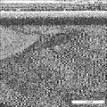
- FIG. 1 is an electron micrograph showing a grain boundary reaction phase.
- a mottled phase different from the parent phase grown along the grain boundary is the grain boundary reaction phase.
- the present invention completed on the basis of the above knowledge is, in one aspect, a copper alloy for electronic parts containing 2.0 to 4.0% by mass of Ti and the balance copper and unavoidable impurities, in the rolling direction by an electron microscope.
- a grain boundary reaction phase containing Ti—Cu-based particles precipitated along the crystal grain boundary, and the largest circle surrounded by the grain boundary reaction phase for each grain boundary reaction phase.
- the average value AvgD 1 is 0.4 to 2.0 ⁇ m
- the grain boundary reaction phase is a copper alloy for electronic parts occupying an area of 1.5 to 15% per 1000 ⁇ m 2 observation field.
- the average value avgd 2 of D 2 is 1.0 ⁇ 5.0 .mu.m.
- the average crystal grain size is 5 ⁇ m or more and 30 ⁇ m or less in terms of equivalent circle diameter, and the grain boundary reaction phase
- the average value AvgD 3 of the diameter D 3 of the largest circle surrounded by the grain boundary of each crystal grain surrounding the crystal grain is AvgD 2 ⁇ AvgD 3 .
- the third element group is selected from the group consisting of Mn, Fe, Mg, Co, Ni, Cr, V, Nb, Mo, Zr, Si, B, and P. One or two or more of these are contained in a total amount of 0 to 0.5% by mass.
- the present invention is a copper product made of the above copper alloy.
- an electronic component comprising the above copper alloy.
- the present invention is a connector comprising the above copper alloy.
- Ti is contained in an amount of 2.0 to 4.0% by mass
- an optional third element group includes Mn, Fe, Mg, Co, Ni, Cr, V, Nb, Mo,
- One to two or more selected from the group consisting of Zr, Si, B, and P is contained in a total amount of 0 to 0.5% by mass, with respect to the copper alloy material consisting of the remaining copper and inevitable impurities, 730
- a solution treatment is performed in which the solid solubility limit of Ti is heated to a temperature equal to or greater than the addition amount
- an aging treatment is performed by heating at a material temperature of 400 to 500 ° C. for 0.1 to 20 hours, Including aging treatment followed by cold rolling at a rolling reduction of 0 to 40%, It is a manufacturing method of the copper alloy for electronic components.
- titanium copper excellent in strength and bending workability can be obtained while depositing a large amount of TiCu 3 which is a stable phase.
- FIG. 1 is a diagram in which the magnification of FIG. 1-1 is reduced.
- Ti content> If Ti is less than 2.0% by mass, a sufficient strengthening mechanism cannot be obtained due to the formation of the original modulation structure of titanium copper, so that sufficient strength cannot be obtained. Conversely, if Ti exceeds 4.0% by mass, coarse TiCu 3 tends to precipitate, and the strength and bending workability tend to deteriorate. Therefore, the content of Ti in the copper alloy according to the present invention is 2.0 to 4.0% by mass, preferably 2.7 to 3.5% by mass. Thus, by optimizing the Ti content, both strength and bending workability suitable for electronic components can be realized.
- ⁇ Third element> When the predetermined third element is added to titanium copper, there is an effect of easily refining crystal grains and improving the strength even when solution treatment is performed at a high temperature at which Ti is sufficiently dissolved. In addition, the predetermined third element promotes the formation of the modulation structure. Furthermore, there is an effect of suppressing rapid coarsening of the Ti—Cu-based stable phase. Therefore, the original age hardening ability of titanium copper can be obtained.
- the third element group one or more selected from the group consisting of Mn, Fe, Mg, Co, Ni, Cr, V, Nb, Mo, Zr, Si, B, and P are added in a total of 0 to It can be contained in an amount of 0.5% by mass, and the total content is preferably 0.05 to 0.5% by mass.
- the grain boundary reaction phase is a phase different from the parent phase formed by aggregation of Ti—Cu-based stable phases precipitated along the grain boundary as grain boundary reaction type particles during the aging treatment.
- the grain boundary reaction phase looks like a mottled pattern.
- the grain boundary reaction phase grows along the crystal grain boundary toward the inside of the grain, the grain boundary reaction phase tends to become longer along the crystal grain boundary as the crystal grain size increases. Further, as the rolling reduction of the final cold rolling increases, the crystal grains extend in the rolling direction, and accordingly, the grain boundary reaction phase tends to become longer in the rolling direction. If the grain boundary reaction phase extends in a specific direction for a long time, the adverse effect on the bending process cannot be reduced. Therefore, it is desirable that the grain boundary reaction phase grows uniformly in all directions.
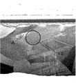
- the grain boundary reaction phase with respect to the diameter D 1 of the maximum circle surrounded by the grain boundary reaction phase for each grain boundary reaction phase in the observation of the structure of the cross section parallel to the rolling direction by an electron microscope.
- the average value Avg (D 2 / D 1 ) of the ratio (D 2 / D 1 ) (hereinafter referred to as “grain boundary reaction phase aspect ratio”) of the diameter D 2 of the smallest circle surrounding the circle is 1.0 to 6.0 Preferably, it is 2.0 to 5.0.
- the circle 11 is the maximum circle surrounded by the grain boundary reaction phase
- the circle 12 is the minimum circle surrounding the grain boundary reaction phase.
- grain boundary reaction phase there are cases where a plurality of grain boundary reaction phases are in contact with each other, but since these are different phases, they can be distinguished by the density of the parent phase of the reflected electron image, element mapping of EPMA, orientation mapping by EBSP, etc. Treat as the grain boundary reaction phase.
- the average value avgd 1 of D 1 is 0.4 ⁇ 2.0 .mu.m, preferably 0.4-1.
- the thickness is 5 ⁇ m, more preferably 0.4 to 1.0 ⁇ m. Further, in the structure observation of the cross section parallel to the rolling direction by the electron microscope, the average value avgd 2 of D 2 in one embodiment, is 1.0 ⁇ 5.0 .mu.m, there preferably 2.0 ⁇ 5.0 .mu.m More preferably, the thickness is 2.0 to 3.0 ⁇ m.
- the grain boundary reaction phase occupies an area of 1.5 to 15%, preferably 1.6 to 10%, per 1000 ⁇ m 2 observation field. More preferably, it occupies an area of 1.7 to 3.2%.
- ⁇ Crystal grain size> In order to improve the strength of titanium copper, the smaller the crystal grains, the better. However, there is a disadvantage that the area ratio of the grain boundary reaction phase tends to increase more than necessary. Therefore, a preferable average crystal grain size is 30 ⁇ m or less, more preferably 20 ⁇ m or less. The lower limit is preferably 1 ⁇ m or more, more preferably 5 ⁇ m or more so that the area ratio of the grain boundary reaction phase does not increase more than necessary.
- the average crystal grain size is represented by a circle-equivalent diameter in a structure observation of a cross section parallel to the rolling direction by an electron microscope.
- the crystal grains have an elliptical shape that extends in the rolling direction in accordance with the rolling reduction in the final cold rolling, but if the rolling reduction becomes high and the crystal grains become extremely flat, the strain increases and causes bending cracking.
- Cheap it is desirable to be as close to a perfect circle as possible. Therefore, in an embodiment of titanium copper according to the present invention, for each crystal grain surrounding the grain boundary reaction phase, an average value AvgD 3 of the diameter D 3 of the maximum circle surrounded by the grain boundary of the crystal grain is defined, and this value Is larger than the average value AvgD 2 of the diameter D 2 of the smallest circle surrounding the grain boundary reaction phase, that is, AvgD 2 ⁇ AvgD 3 . In this case, bending workability is not impaired.
- the circle 13 is the maximum circle surrounded by the grain boundaries of the crystal grains surrounding the grain boundary reaction phase.
- the copper alloy according to the present invention can be provided as various copper products, such as plates, strips, tubes, rods and wires.
- the titanium copper according to the present invention is not limited, but can be suitably used as a material for electronic components such as switches, connectors, jacks, terminals, and relays.
- Titanium copper according to the present invention can be produced by carrying out appropriate heat treatment and cold rolling, particularly in the final solution treatment and the subsequent steps. Below, a suitable manufacture example is demonstrated one by one for every process.
- Ingot production by melting and casting is basically performed in a vacuum or in an inert gas atmosphere. If the additive element remains undissolved during melting, it does not effectively act on strength improvement. Therefore, in order to eliminate undissolved residue, it is necessary to add a high melting point third element such as Fe or Cr, and after sufficiently stirring, hold for a certain period of time. On the other hand, since Ti is relatively easily dissolved in Cu, it may be added after the third element is dissolved. Therefore, Cu includes one or more selected from the group consisting of Mn, Fe, Mg, Co, Ni, Cr, V, Nb, Mo, Zr, Si, B and P in total from 0 to 0. It is desirable to add in an amount of 50% by mass, and then add Ti in an amount of 2.0 to 4.0% by mass to produce an ingot.
- the solution treatment After appropriately repeating cold rolling and annealing.
- the reason why the solution treatment is performed in advance is to reduce the burden in the final solution treatment. That is, in the final solution treatment, it is not a heat treatment for dissolving the second phase particles, but is already in solution, so it is only necessary to cause recrystallization while maintaining that state.
- the first solution treatment may be performed at a heating temperature of 850 to 900 ° C. for 2 to 10 minutes. In this case, it is preferable to increase the heating rate and the cooling rate as much as possible so that the second phase particles do not precipitate. Note that the first solution treatment may not be performed.
- the heating temperature is the second phase.
- the temperature is close to the solid solubility limit of the particle composition (the temperature at which the solid solubility limit of Ti becomes equal to the addition amount in the range of 2.0 to 4.0% by mass of Ti is about 730 to 840 ° C., For example, when the added amount of Ti is 3.2 mass%, it is about 800 ° C.). And if it heats rapidly to this temperature and a cooling rate is also made fast, generation
- grains will be suppressed.
- heating is performed at a temperature at which the solid solubility limit of Ti at 730 to 880 ° C. is equal to the addition amount, and more typically, the solid solubility limit of Ti at 730 to 880 ° C. is the same as the addition amount. It is heated to a temperature 0 to 20 ° C. higher, preferably 0 to 10 ° C. higher than the temperature at which
- the shorter the heating time in the final solution treatment the finer the crystal grains.
- the heating time can be, for example, 30 to 90 seconds, and typically 30 to 60 seconds. At this point, it is preferable that the second phase particles are not generated as much as possible. A higher cooling rate is preferable, and it is advantageous to use water cooling from the viewpoint of operational stability.
- Aging treatment An aging treatment is performed following the final solution treatment.
- cold rolling is usually performed after the final solution treatment, but in order to obtain titanium copper according to the present invention, aging is immediately performed without performing cold rolling after the final solution treatment. It is preferable to carry out the treatment.
- cold rolling at a high workability was performed to maintain elongation and obtain high strength, but bending workability was deteriorated.
- the degree of work is lowered in order to maintain the bending workability, not only the strain distribution becomes non-uniform, but also the strength rise is small.
- the aging treatment is preferably performed at a temperature slightly higher than the conventional aging conditions so that Ti—Cu-based stable phases precipitated by the grain boundary reaction gather and the grain boundary reaction phase grows to an appropriate size.
- the grain boundary reaction phase grows along the grain boundary (D 2 increases) and grows thinly (D 1 is small) toward the grain, so Avg (D 2 / D 1 ) tends to increase. .
- final cold rolling After the aging treatment, final cold rolling is performed.
- the strength of titanium copper can be increased by the final cold working. This cold rolling need not be carried out, but in order to obtain high strength, the rolling reduction is set to 5% or more, preferably 10% or more, more preferably 15% or more. However, if the rolling reduction is too high, the grain boundary reaction phase aspect ratio becomes too large, so the rolling reduction is 40% or less, preferably 30% or less, more preferably 25% or less.
- a structure that guarantees contact pressure at a site that is not subjected to plastic deformation during shape processing after press punching eg, a structure in which the distance between the contact part of the terminal and the bent part (arm) is long, or a fork-type terminal
- a high spring limit value is important because resistance to bending deflection is required. Therefore, in applications where the spring limit value is particularly important, strain relief annealing is performed after the final cold rolling. In particular, when the rolling reduction of the final cold rolling is 3% or more, it is preferable to perform strain relief annealing in applications where the spring limit value is important.
- strain relief annealing when the rolling reduction of the final cold rolling is 10% or more, it is particularly preferable to perform strain relief annealing in applications where the spring limit value is important. Although dislocations introduced by cold rolling are unevenly distributed, dislocations are rearranged by performing strain relief annealing, which can further increase the strength. However, excessive strain relief annealing is not preferable because dislocations disappear and strength decreases.
- the conditions for strain relief annealing may be conventional conditions. Specifically, it is preferably performed under the conditions of heating at a material temperature of 200 ° C. or more and less than 400 ° C. for 0.001 to 20 hours. It is more preferable to carry out under conditions of heating at a material temperature of 200 to 300 ° C. for 12 to 20 hours, and at a high temperature for a short time (eg, heating at a material temperature of 300 to 400 ° C. for 0.001 to 12 hours).
- steps such as grinding, polishing, and shot blast pickling for removing oxide scale on the surface can be appropriately performed between the above steps.
- Ti which is an active metal
- a vacuum melting furnace was used for melting.
- raw materials having a relatively high purity were carefully selected and used.
- the intermediate plate thickness is adjusted so that the final plate thickness is 0.10 mm, cold rolling is performed, and then inserted into an annealing furnace capable of rapid heating to perform the final solution treatment. And then water cooled.
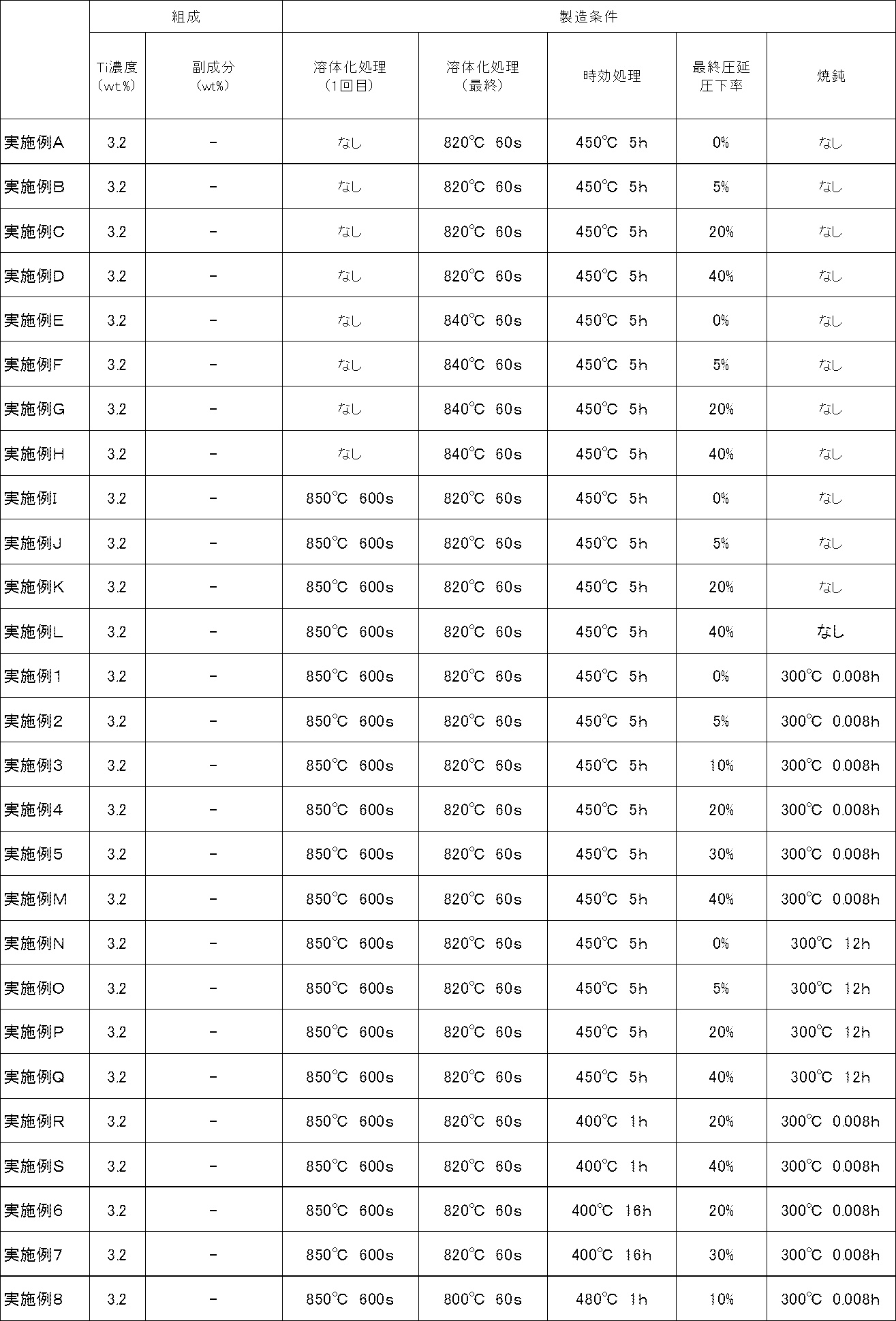
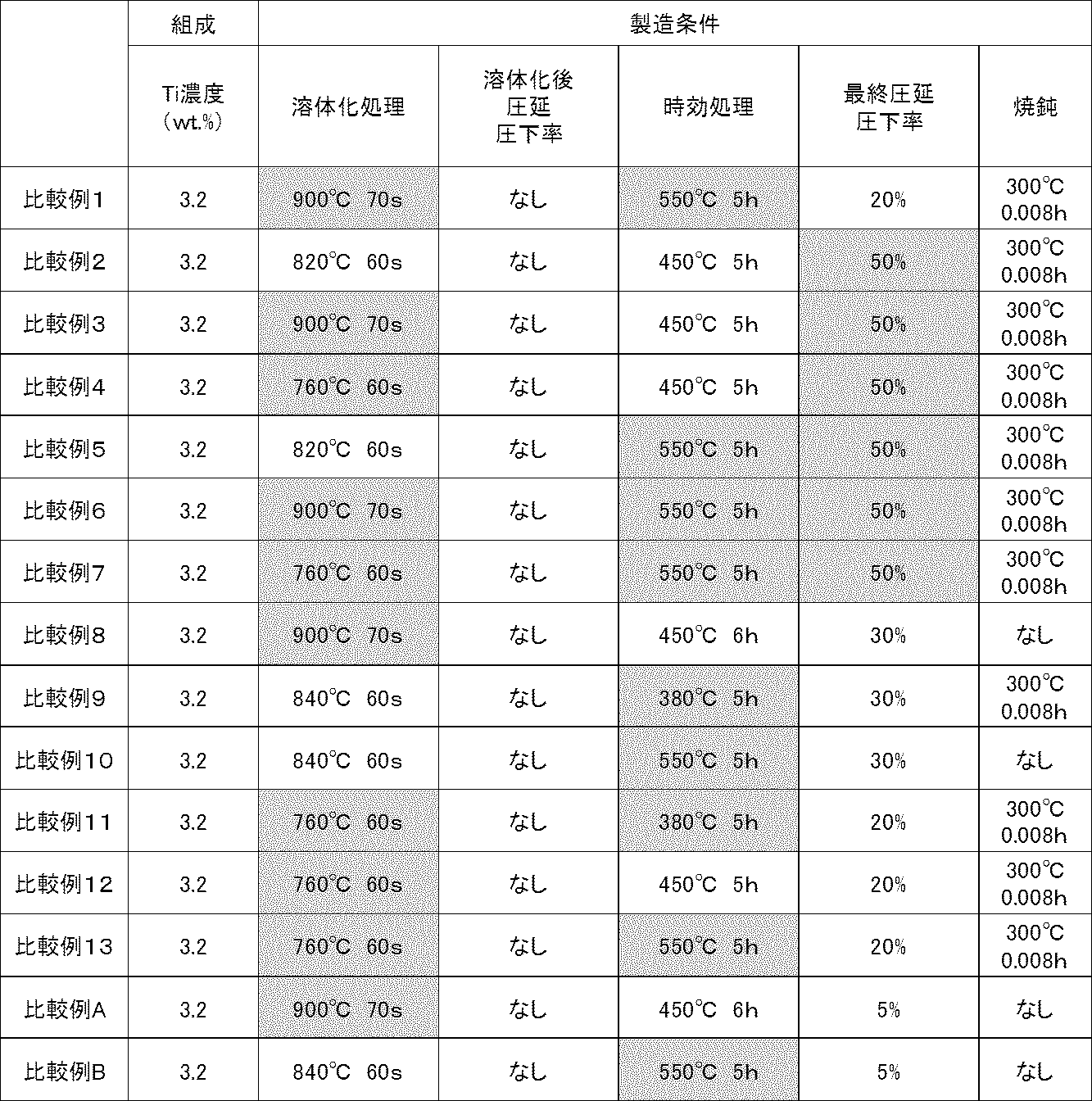
- the heating conditions at this time were such that the material temperature was such that the solid solubility limit of Ti was the same as the amount added (Ti concentration: 3.2% by mass, about 800 ° C., Ti concentration: 2.0% by mass, about 730 ° C .; Each sample was held for 1 minute under the heating conditions shown in Table 1 on the basis of 0.0 mass% and about 840 ° C.). (See Table 1).
- test pieces of invention examples and comparative examples were obtained by cold rolling after solution treatment under the conditions described in Table 1, an aging treatment was performed under the conditions described in Table 1 in an Ar atmosphere. After descaling by pickling, final cold rolling was performed under the conditions described in Table 1, and finally, annealing was performed under the respective heating conditions described in Table 1 to obtain test pieces of invention examples and comparative examples.
- ⁇ Average crystal grain size The average crystal grain size is measured by cutting a cross section parallel to the rolling direction with FIB, exposing the cross section, observing the cross section with SIM, and counting the number of crystal grains per unit area.
- the average equivalent circle diameter was obtained. Specifically, a frame of 100 ⁇ m ⁇ 100 ⁇ m was created, and the number of crystal grains present in this frame was counted. Note that all the crystal grains crossing the frame were counted as 1 ⁇ 2.
- the average value of the area per crystal grain is obtained by dividing the frame area of 10,000 ⁇ m 2 by the total. Since the diameter of the perfect circle having the area is the equivalent circle diameter, this was defined as the average crystal grain size.
- ⁇ Grain boundary reaction phase> The cross section parallel to the rolling direction was cut with FIB to expose the cross section, and then the cross section was observed with SIM, and an observation visual field of 100 ⁇ m ⁇ 100 ⁇ m was photographed. It was confirmed by an attached EDS (Energy Dispersive X-ray Spectrometer) that the black part constituting the mottled pattern of the grain boundary reaction phase was TiCu 3 .
- EDS Electronic Dispersive X-ray Spectrometer
- the diameter D 1 of the maximum circle surrounded by the grain boundary reaction phase and the diameter D 2 of the minimum circle surrounding the grain boundary reaction phase are measured on the photograph, respectively. It was determined the 2 / D 1.
- Examples 1 to 5 or Examples 6 to 7 it can be seen that Avg (D 2 / D 1 ) increases as the rolling reduction of the final rolling increases.
- the final solution treatment was performed at 800 ° C. ⁇ 60 s, and the average particle size was smaller than that in Examples 1 to 7.
- the average particle size was larger than in Examples 1-7.
- Examples 13 and 14 it can be seen that increasing the Ti concentration tends to increase the strength.
- Examples 15 to 17 are examples in which a third element was added. It can be understood that the effect of the present invention is maintained even when the third element is added.
- Example A to H neither the primary solution treatment nor the strain relief annealing was performed, but the titanium copper according to the present invention having an excellent balance between strength and bending workability was obtained. However, since the strain relief annealing was not performed, the kb value was smaller than the example in which the strain relief annealing was performed. In Examples I to L, strain relief annealing was not performed, but titanium copper according to the present invention having an excellent balance between strength and bending workability was obtained. Similarly, the kb value was small.
- Example M was an example in which the rolling reduction of the final rolling was increased to 40% with respect to Example 5, and the strength was slightly improved.
- Examples N to Q are examples in which the strain relief annealing time is longer than those in Examples 1 to 5 and M, and it can be seen that the spring limit value is slightly improved when compared at the same rolling reduction.
- Examples R and S are examples in which the aging treatment was performed on the low temperature side, and the area of the grain boundary reaction phase was reduced as compared with Examples 4 and M, respectively, but the balance between strength and bending workability was still a comparative example.
- Example T is an example in which the aging treatment was performed for a long time as compared with Example 9, and the area of the grain boundary reaction phase increased, but the balance between strength and bending workability is still superior compared to the comparative example. .
- Example U is an example in which a high reduction ratio in the final cold rolling as compared with Example 9, the diameter D 2 of the smallest circle enclosing the grain boundary reaction phase is slightly larger, still strength and bending workability The balance is superior to the comparative example.
- Example V the time for aging treatment is longer than that in Example 9 and the rolling reduction of the final cold rolling is high, but the balance between strength and bending workability is still excellent as compared with the comparative example.
- Examples W to Y since the temperature of the final solution treatment was set on the high temperature side, the average crystal grains were slightly larger, but the balance between strength and bending workability is still superior compared to the comparative example.
- Examples Z and A ′ are examples in which the Ti concentration was 4.0% by mass, and the titanium copper according to the present invention having an excellent balance between strength and bending workability was obtained.
- Comparative Examples 1 to 8 are examples in which the aging treatment was performed without performing the cold rolling after the final solution treatment as in the examples, but because the heat treatment conditions and / or the rolling conditions were not appropriate in each case. This is an example in which the strength and bending workability are not sufficiently improved.
- Comparative Example 1 since the solution treatment temperature and the aging temperature were too high, the grain boundary reaction phase was coarsened, the area ratio of the grain boundary reaction phase was large, and the crystal grains were also large.
- Comparative Example 2 since the rolling reduction in the final rolling was too high, the grain boundary reaction phase and the crystal grains were flattened.
- Comparative Example 3 since the rolling reduction in the final rolling was too high, the grain boundary reaction phase was flattened. Since the solution treatment temperature is high, the crystal grains are large. Since the crystal grain is large, the grain boundary area is reduced, the grain boundary reaction phase is reduced, and the area ratio of the grain boundary reaction phase is reduced for the same reason. In Comparative Example 4, since the solution treatment temperature was low, the crystal grains were small, and the rolling reduction in the final rolling was too high, so that the grain boundary reaction phase and the crystal grains were flattened. In Comparative Example 5, since the rolling reduction in the final rolling was too high, the grain boundary reaction phase and the crystal grains were flattened. Moreover, since the aging temperature was too high, the grain boundary reaction phase became coarse.
- Comparative Example 6 since the rolling reduction in the final rolling was too high, the grain boundary reaction phase and the crystal grains were flattened. Moreover, since the solution treatment temperature and the aging temperature were too high, the grain boundary reaction phase was coarsened, the area ratio of the grain boundary reaction phase was large, and the crystal grains were also large. In Comparative Example 7, since the solution treatment temperature is low, the crystal grains are small, and since the aging treatment temperature is high, the grain boundary reaction phase is coarsened, and the rolling reduction in the final rolling is too high. Flattened. In Comparative Example 8, since the solution temperature was too high, the crystal grain size was coarsened and ideal aging was performed. However, the reaction phase was formed along the grain boundary, so that the grain boundary reaction phase was flattened.
- Comparative Example A is an example in which the reduction ratio in the final cold rolling was reduced as compared with Comparative Example 8, but the crystal grain size was increased and Avg (D 2 / D 1 ) was increased as in Comparative Example 8.
- Comparative Example B is an example in which the rolling reduction in the final cold rolling was made smaller than that of Comparative Example 10, but Avg (D 2 / D 1 ) was still large, and balanced characteristics could not be obtained.
Landscapes
- Chemical & Material Sciences (AREA)
- Engineering & Computer Science (AREA)
- Materials Engineering (AREA)
- Mechanical Engineering (AREA)
- Metallurgy (AREA)
- Organic Chemistry (AREA)
- Physics & Mathematics (AREA)
- Thermal Sciences (AREA)
- Crystallography & Structural Chemistry (AREA)
- Conductive Materials (AREA)
- Non-Insulated Conductors (AREA)
Abstract
Description
溶体化処理に続いて、材料温度400~500℃で0.1~20時間加熱する時効処理を行い、
時効処理に続いて、圧下率0~40%の冷間圧延を行うことを含む、
電子部品用銅合金の製造方法である。
Tiが2.0質量%未満ではチタン銅本来の変調構造の形成による強化機構を充分に得ることができないことから十分な強度が得られず、逆に4.0質量%を超えると粗大なTiCu3が析出し易くなり、強度及び曲げ加工性が劣化する傾向にある。従って、本発明に係る銅合金中のTiの含有量は2.0~4.0質量%であり、好ましくは2.7~3.5質量%である。このようにTiの含有量を適正化することで、電子部品用に適した強度及び曲げ加工性を共に実現することができる。
所定の第3元素をチタン銅に添加すると、Tiが十分に固溶する高い温度で溶体化処理をしても結晶粒が容易に微細化し、強度を向上させる効果がある。また、所定の第3元素は変調構造の形成を促進する。更に、Ti-Cu系の安定相の急激な粗大化を抑制する効果もある。そのため、チタン銅本来の時効硬化能が得られるようになる。
粒界反応相は、時効処理時に粒界反応型の粒子として結晶粒界に沿って析出したTi-Cu系の安定相同士が集合してできた、母相とは異なる相である。粒界反応相を電子顕微鏡で観察すると、まだら模様に見える。粒界反応相を所定の大きさ及び形状に制御することによって、Ti-Cu系の安定相による悪影響が軽減若しくは無害化される。
チタン銅の強度を向上させるためには結晶粒が小さいほどよいが、粒界反応相の面積率が必要以上に上昇しやすくなる不都合が生じる。そこで、好ましい平均結晶粒径は30μm以下、より好ましくは20μm以下である。下限は粒界反応相の面積率が必要以上に上昇しないように1μm以上とするのが好ましく、より好ましくは5μm以上である。本発明において、平均結晶粒径は電子顕微鏡による圧延方向に平行な断面の組織観察における円相当径で表す。
本発明に係る銅合金は種々の伸銅品、例えば板、条、管、棒及び線として提供されることができる。本発明に係るチタン銅は、限定的ではないが、スイッチ、コネクタ、ジャック、端子、リレー等の電子部品の材料として好適に使用することができる。
本発明に係るチタン銅は、特に最終の溶体化処理及びそれ以降の工程で適切な熱処理及び冷間圧延を実施することにより製造可能である。以下に、好適な製造例を工程毎に順次説明する。
溶解及び鋳造によるインゴットの製造は、基本的に真空中又は不活性ガス雰囲気中で行う。溶解において添加元素の溶け残りがあると、強度の向上に対して有効に作用しない。よって、溶け残りをなくすため、FeやCr等の高融点の第3元素は、添加してから十分に攪拌したうえで、一定時間保持する必要がある。一方、TiはCu中に比較的溶け易いので第3元素の溶解後に添加すればよい。従って、Cuに、Mn、Fe、Mg、Co、Ni、Cr、V、Nb、Mo、Zr、Si、B及びPよりなる群から選択される1種又は2種以上を合計で0~0.50質量%含有するように添加し、次いでTiを2.0~4.0質量%含有するように添加してインゴットを製造することが望ましい。
インゴット製造時に生じた凝固偏析や晶出物は粗大なので均質化焼鈍でできるだけ母相に固溶させて小さくし、可能な限り無くすことが望ましい。これは曲げ割れの防止に効果があるからである。
具体的には、インゴット製造工程後には、900~970℃に加熱して3~24時間均質化焼鈍を行った後に、熱間圧延を実施するのが好ましい。液体金属脆性を防止するために、熱延前及び熱延中は960℃以下とし、且つ、元厚から全体の圧下率が90%までのパスは900℃以上とするのが好ましい。そして、パス毎に適度な再結晶を起こしてTiの偏析を効果的に低減するために、パスごとの圧下量を10~20mmで実施するとよい。
その後、冷延と焼鈍を適宜繰り返してから溶体化処理を行うのが好ましい。ここで予め溶体化を行っておく理由は、最終の溶体化処理での負担を軽減させるためである。すなわち、最終の溶体化処理では、第二相粒子を固溶させるための熱処理ではなく、既に溶体化されてあるのだから、その状態を維持しつつ再結晶のみ起こさせればよいので、軽めの熱処理で済む。具体的には、第一溶体化処理は加熱温度を850~900℃とし、2~10分間行えばよい。そのときの昇温速度及び冷却速度においても極力速くし、ここでは第二相粒子が析出しないようにするのが好ましい。なお、第一溶体化処理は行わなくても良い。
最終の溶体化処理前の中間圧延における圧下率を高くするほど、最終の溶体化処理における再結晶粒が均一かつ微細に生成するので、中間圧延の圧下率は高めに設定する。好ましくは70~99%ある。圧下率は{((圧延前の厚み-圧延後の厚み)/圧延前の厚み)×100%}で定義される。
最終の溶体化処理では、析出物を完全に固溶させることが望ましいが、完全に無くすまで高温に加熱すると、結晶粒が粗大化しやすいので、加熱温度は第二相粒子組成の固溶限付近の温度とする(Tiの添加量が2.0~4.0質量%の範囲でTiの固溶限が添加量と等しくなる温度は730~840℃程度であり、例えばTiの添加量が3.2質量%では800℃程度)。そしてこの温度まで急速に加熱し、冷却速度も速くすれば粗大な第二相粒子の発生が抑制される。従って、典型的には、730~880℃のTiの固溶限が添加量と同じになる温度以上に加熱し、より典型的には730~880℃のTiの固溶限が添加量と同じになる温度に比べて0~20℃高い温度、好ましくは0~10℃高い温度に加熱する。
最終の溶体化処理に引き続いて、時効処理を行う。従来は最終の溶体化処理の後は冷間圧延を行うことが通例であったが、本発明に係るチタン銅を得る上では最終の溶体化処理の後、冷間圧延を行わずに直ちに時効処理を行うことが好ましい。従来は伸びを維持して高強度を得るために高加工度の冷間圧延を行っていたが、曲げ加工性が劣化していた。曲げ加工性を維持するために加工度を低くすると、歪の分布が不均一になるばかりでなく、強度上昇も小さい。これは時効処理の前に低加工度の冷間圧延を行うと、加工歪が不均一に分布しやすく、変調構造の形成が不均一となって、曲げ歪に対する抵抗が弱くなるだけでなく、粒界反応相が発達しにくいからである。時効処理は粒界反応で析出したTi-Cu系の安定相が集合して粒界反応相が適切な大きさに成長するように、慣例の時効条件よりもやや高温で行うとよい。低温時効すると粒界反応相が粒界に沿って成長し(D2が大きくなり)、粒内に向かって薄く(D1は小さい)成長するのでAvg(D2/D1)が大きくなりやすい。具体的には、材料温度400~500℃で0.1~20時間加熱することが好ましく、材料温度400~480℃で1~16時間加熱することがより好ましい。
上記時効処理後、最終の冷間圧延を行う。最終の冷間加工によってチタン銅の強度を高めることができる。この冷間圧延は実施しなくてもよいが、高い強度を得ることを目的とする場合は圧下率を5%以上、好ましくは10%以上、より好ましくは15%以上とする。但し、圧下率が高すぎると粒界反応相アスペクト比が大きくなり過ぎることから、圧下率を40%以下、好ましくは30%以下、より好ましくは25%以下とする。
電子部品の構造に応じて、異なる形状加工が要求される。一般に曲げ加工やノッチ加工などの塑性変形を施された部位は加工硬化し、素材の強度はより上昇する。このような曲げ加工部で接圧を担保する構造では塑性変形しにくいので、高いばね限界値は不要である。そのため、このような用途では歪取焼鈍は行わなくても良い。
一方、プレス打ち抜き後の形状加工時に塑性変形を受けない部位で接圧を担保する構造(例:端子の接点部から曲げ加工部までの直線部分(アーム)の距離が長い構造、またはフォーク型端子のようにノッチ加工や曲げ加工が施されない構造であって、曲げ応力がアームにかかるような構造)では、曲げたわみに対する抵抗が必要となるので高いばね限界値が重要となる。
従って、特にばね限界値が重要となる用途では最終の冷間圧延の後、歪取焼鈍を行う。特に最終の冷間圧延の圧下率が3%以上の場合には、ばね限界値が重要となる用途では歪取焼鈍を行うことが好ましい。また、最終の冷間圧延の圧下率が10%以上の場合には、ばね限界値が重要となる用途では歪取焼鈍を行うことが特に好ましい。冷間圧延で導入された転位は不均一に分布しているが、歪取焼鈍を行うことで転位が再配列し、これにより更に強度上昇を図ることもできる。ただし、過度の歪取焼鈍を行うと転位が消滅して強度が低下するため好ましくない。
歪取焼鈍の条件は慣用の条件でよいが、具体的には、材料温度200℃以上400℃未満で0.001~20時間加熱の条件で行うのが好ましく、低温であれば長時間(例えば材料温度200~300℃で12~20時間加熱)、高温であれば短時間(例えば材料温度300~400℃で0.001~12時間加熱)の条件で行うのがより好ましい。

<強度>
引張方向が圧延方向と平行になるように、プレス機を用いてJIS13B号試験片を作製した。JIS-Z2241に従ってこの試験片の引張試験を行ない、圧延平行方向の0.2%耐力(YS)を測定した。
<曲げ加工性>
JIS H 3130に従って、Badway(曲げ軸が圧延方向と同一方向)のW曲げ試験を行って割れの発生しない最小半径(MBR)の板厚(t)に対する比であるMBR/t値を測定した。
<平均結晶粒径>
平均結晶粒径の測定は、圧延方向に平行な断面をFIBにて切断することで、断面を露出した後、断面をSIM観察し、単位面積当たりの結晶粒の数をカウントして、結晶粒の平均の円相当径を求めた。具体的には、100μm×100μmの枠を作成し、この枠の中に存在する結晶粒の数をカウントした。なお、枠を横切っている結晶粒については、すべて1/2個としてカウントした。枠の面積10000μm2をその合計で除したものが結晶粒1個当たりの面積の平均値である。その面積を持つ真円の直径が円相当径であるので、これを平均結晶粒径とした。
<粒界反応相>
圧延方向に平行な断面をFIBにて切断することで、断面を露出した後、断面をSIM観察し、観察視野100μm×100μmを撮影した。粒界反応相のまだら模様を構成する黒色部分が、TiCu3であることを付属のEDS(Energy Dispersive X-ray Spectrometer)により確認した。
個々の粒界反応相について、粒界反応相に取り囲まれる最大円の直径D1と粒界反応相を取り囲む最小円の直径D2をそれぞれ写真上で測定し、個々の粒界反応相についてD2/D1を求めた。観察視野中に含まれ、D1及びD2を測定可能なすべての粒界反応相に対してD2/D1を求め、その平均値をAvg(D2/D1)とした。また、測定したD1及びD2の平均値をそれぞれAvgD1及びAvgD2とした。
また、粒界反応相を取り囲む各結晶粒について該結晶粒の粒界に取り囲まれる最大円の直径D3をそれぞれ写真上で測定し、観察視野中で測定可能なすべてのD3の平均値をAvgD3とした。
また、上記写真上の任意の1000μm2の観察視野中で粒界反応相が占める面積を画像解析装置により求め、5箇所の平均値を算出し、これを粒界反応相の1000μm2の観察視野当たりの面積とした。
<ばね限界値(Kb)>
ばね限界値(Kb)は、JIS H3130(合金番号C1990)に準拠して、繰り返し式たわみ試験を実施し、永久歪が残留する曲げモーメントから表面最大応力を測定した。
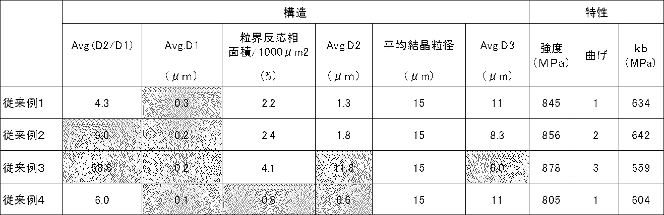


従来例1~4は、Ti-Cu系の安定相が粒界で未固溶粒子としてCu母相中に散在する条件として、最終の溶体化処理と時効処理の間に冷間圧延を行った例である。この場合は、粒界反応相の成長は小さく、面積率も小さめであった。強度及び曲げ加工性のバランスも悪い。
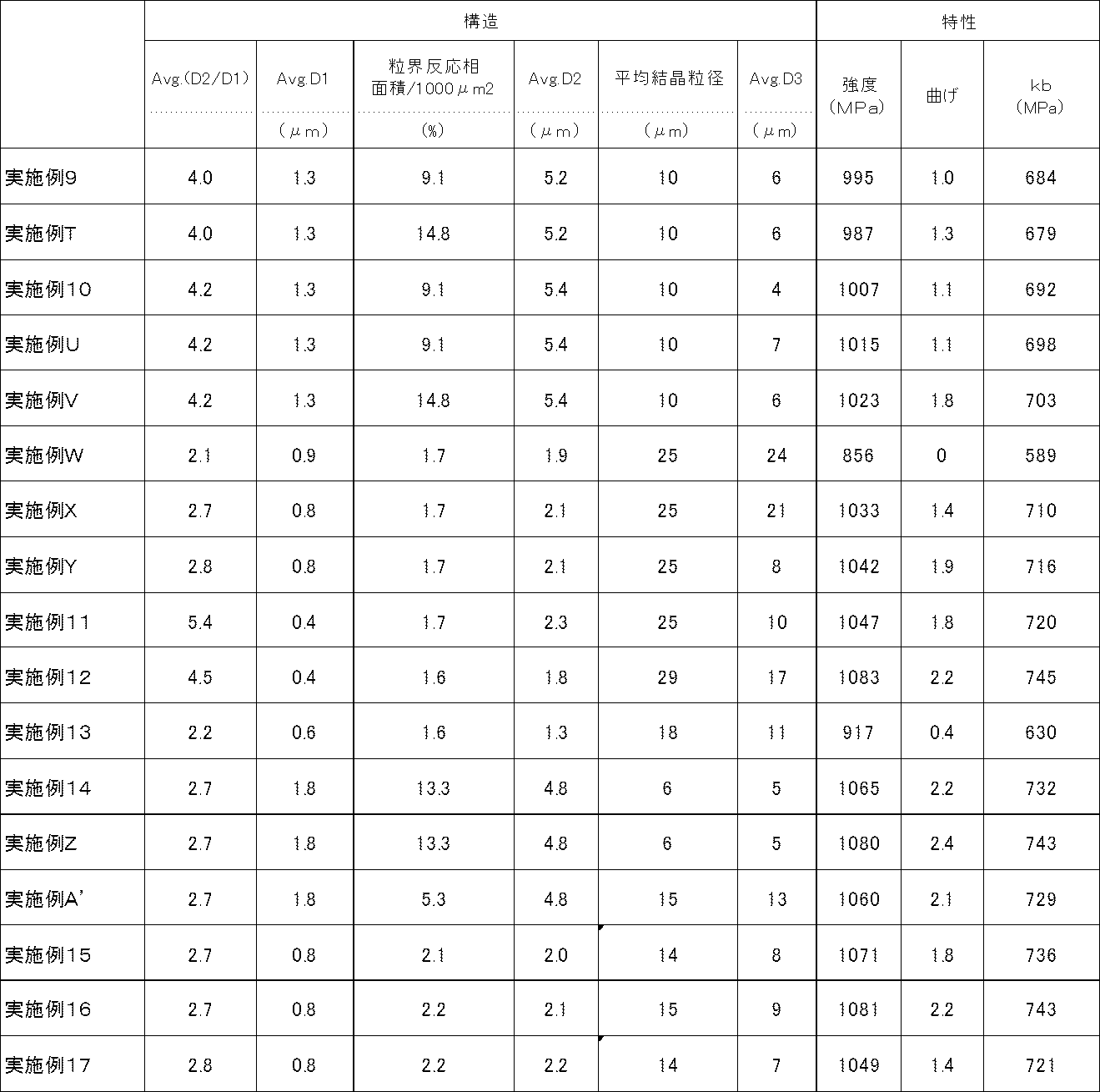
実施例1~17は、最終の溶体化処理後に冷間圧延を行わずに時効処理を行った例である。実施例1~7は最終溶体化処理を820℃×60sに固定して時効処理及び最終圧延の条件を変化させた。いずれの実施例も強度と曲げ加工性のバランスが従来例に比べて顕著に向上していることが分かる。
また、実施例1~5又は実施例6~7より、最終圧延の圧下率が上昇するにつれてAvg(D2/D1)が上昇することが分かる。
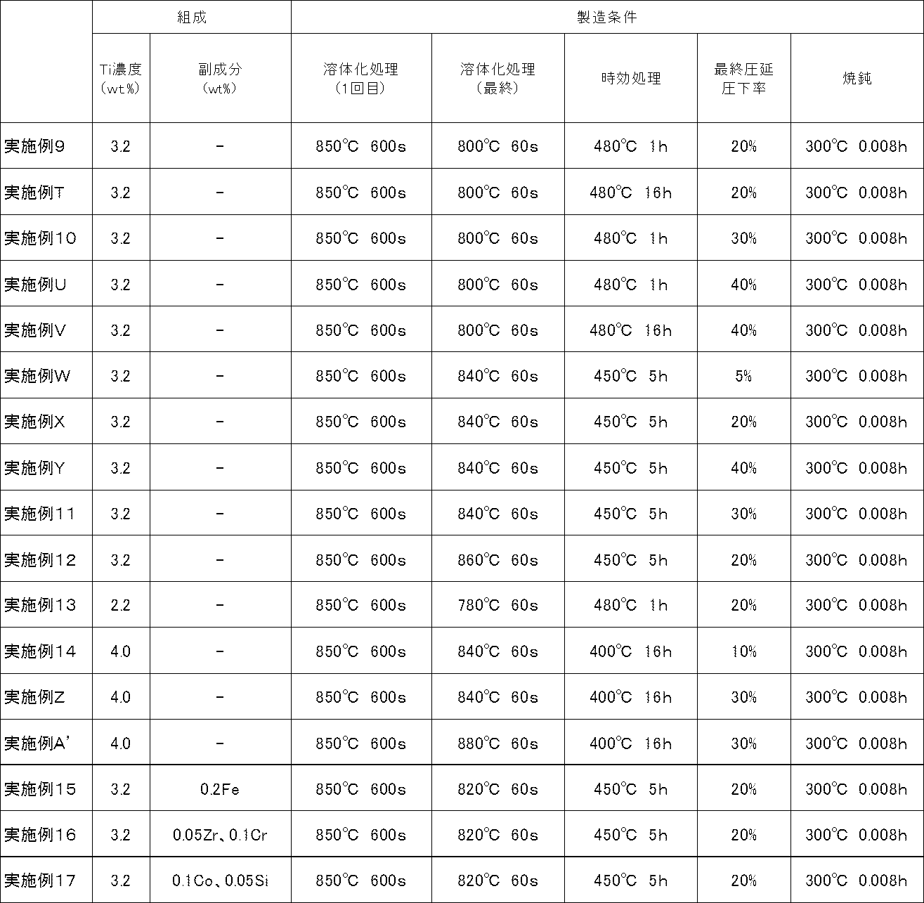
実施例8~10は、最終溶体化処理を800℃×60sとした例であり、実施例1~7に比べて平均粒径が小さくなった。実施例11~12では逆に最終溶体化処理の温度を高くしたので、実施例1~7に比べて平均粒径が大きくなった。
実施例13及び14から、Ti濃度を上げると強度が上昇する傾向にあることが分かる。
実施例15~17は第三元素を添加した例である。第三元素を添加しても本発明の効果が維持されることが理解できる。
実施例A~Hは、第1次溶体化処理及び歪取焼鈍の何れも行わなかったが、強度と曲げ加工性のバランスに優れた本発明に係るチタン銅が得られた。但し、歪取焼鈍を行わなかったので、歪取焼鈍を行った例に比べてkb値は小さかった。
実施例I~Lは、歪取焼鈍を行わなかったが、強度と曲げ加工性のバランスに優れた本発明に係るチタン銅が得られた。同様に、kb値は小さかった。
実施例Mは、実施例5に対して最終圧延の圧下率を40%に高めた例であり、強度が若干向上した。
実施例N~Qは、実施例1~5及びMに比べて歪取焼鈍時間を長めに行った例であり、同一圧下率で比べるとばね限界値が若干向上したことが分かる。
実施例R及びSは、時効処理を低温側で行った例であり、実施例4及びMに比べて粒界反応相の面積がそれぞれ減少したが、依然として強度と曲げ加工性のバランスは比較例に比べて優れている。
実施例Tは、実施例9に比べて時効処理を長時間行った例であり、粒界反応相の面積が増大したが、依然として強度と曲げ加工性のバランスは比較例に比べて優れている。
実施例Uは、実施例9に比べて最終冷間圧延の圧下率を高くした例であり、粒界反応相を取り囲む最小円の直径D2がやや大きくなったが、依然として強度と曲げ加工性のバランスは比較例に比べて優れている。
実施例Vは、実施例9に比べて時効処理の時間が長く、最終冷間圧延の圧下率も高いが、依然として強度と曲げ加工性のバランスは比較例に比べて優れている。
実施例W~Yは、最終溶体化処理の温度を高温側で設定したため、平均結晶粒がやや大きくなったが、依然として強度と曲げ加工性のバランスは比較例に比べて優れている。
実施例Z及びA’はTi濃度を4.0質量%とした例であるが、強度と曲げ加工性のバランスに優れた本発明に係るチタン銅が得られた。
比較例1~8は実施例と同様に最終の溶体化処理後に冷間圧延を行わずに時効処理を行った例であるが、いずれも熱処理条件及び/又は圧延条件が不適切であったために、強度及び曲げ加工性が十分に向上していない例である。
比較例1は溶体化処理温度及び時効温度が高すぎたため、粒界反応相が粗大化し、粒界反応相の面積率が大きく、結晶粒も大きかった。
比較例2は最終圧延における圧下率が高すぎたため、粒界反応相及び結晶粒が扁平化した。
比較例3は最終圧延における圧下率が高すぎたため、粒界反応相が扁平化した。溶体化処理温度が高いため、結晶粒が大きい。結晶粒が大きいので粒界面積が減少し、粒界反応相は小さくなり、同様の理由で粒界反応相の面積率は小さくなった。
比較例4は溶体化処理温度が低いため、結晶粒が小さくなり、また、最終圧延における圧下率が高すぎたため、粒界反応相及び結晶粒が扁平化した。
比較例5は最終圧延における圧下率が高すぎたため、粒界反応相及び結晶粒が扁平化した。また、時効温度が高すぎたため、粒界反応相が粗大化した。
比較例6は最終圧延における圧下率が高すぎたため、粒界反応相及び結晶粒が扁平化した。また、溶体化処理温度及び時効温度が高すぎたため、粒界反応相が粗大化し、粒界反応相の面積率が大きく、結晶粒も大きかった。
比較例7は溶体化処理温度が低いため結晶粒が小さくなり、時効処理温度が高いため、粒界反応相が粗大化し、最終圧延における圧下率が高すぎたため、粒界反応相及び結晶粒が扁平化した。
比較例8は溶体化温度が高すぎたため結晶粒径が粗大化し、理想的な時効を行ったが、粒界に沿って反応相を形成したため粒界反応相が扁平化した。粒径が大きいので時効処理中に粒界まで拡散する距離が長くなり、反応相へのTi原子の供給が不足したことにより粒界反応相の面積率が低かった。
比較例9は時効処理温度が低かったため、Avg(D2/D1)が大きくなり粒界反応相の形状が不適切であり、曲げが劣化した。
比較例10は時効処理温度が高すぎたため、AvgD2が大きくなり粒界反応相が粗大化した。
比較例11~13では溶体化処理温度を低く設定しながら時効処理温度を変化させた。結晶粒径が小さいのに加えて、粒界反応相の面積割合が不適切であった。
比較例Aは比較例8に対して最終冷間圧延における圧下率を小さくした例であるが、比較例8と同様に結晶粒径が粗大化し、Avg(D2/D1)も大きくなった。
比較例Bは比較例10に対して最終冷間圧延における圧下率を小さくした例であるが、依然としてAvg(D2/D1)が大きく、バランスの取れた特性は得られなかった。
12 粒界反応相を取り囲む最小円
13 粒界反応相を取り囲む結晶粒の粒界に取り囲まれる最大円
Claims (8)
- Tiを2.0~4.0質量%含有し、残部銅及び不可避的不純物からなる電子部品用銅合金であって、電子顕微鏡による圧延方向に平行な断面の組織観察において、結晶粒界に沿って析出したTi-Cu系粒子を含む粒界反応相が存在し、個々の粒界反応相についての粒界反応相に取り囲まれる最大円の直径D1に対する粒界反応相を取り囲む最小円の直径D2の比(D2/D1)の平均値Avg(D2/D1)が1.0~6.0であり、D1の平均値AvgD1が0.4~2.0μmであり、更に、粒界反応相が1000μm2の観察視野当たり1.5~15%の面積を占める電子部品用銅合金。
- 電子顕微鏡による圧延方向に平行な断面の組織観察において、D2の平均値AvgD2が1.0~5.0μmである請求項1記載の銅合金。
- 電子顕微鏡による圧延方向に平行な断面の組織観察において、平均結晶粒径が円相当径で表して5μm以上30μm以下であり、粒界反応相を取り囲む各結晶粒について該結晶粒の粒界に取り囲まれる最大円の直径D3の平均値AvgD3が、AvgD2<AvgD3である請求項1又は2記載の銅合金。
- 第3元素群としてMn、Fe、Mg、Co、Ni、Cr、V、Nb、Mo、Zr、Si、B及びPよりなる群から選択される1種又は2種以上を合計で0~0.5質量%含有する請求項1~3何れか一項記載の銅合金。
- 請求項1~4何れか一項記載の銅合金からなる伸銅品。
- 請求項1~4何れか一項記載の銅合金を備えた電子部品。
- 請求項1~4何れか一項記載の銅合金を備えたコネクタ。
- Tiを2.0~4.0質量%含有し、随意的な第3元素群としてMn、Fe、Mg、Co、Ni、Cr、V、Nb、Mo、Zr、Si、B及びPよりなる群から選択される1種又は2種以上を合計で0~0.5質量%含有し、残部銅及び不可避的不純物からなる銅合金素材に対して、730~880℃でTiの固溶限が添加量と同じになる温度以上に加熱する溶体化処理を行い、
溶体化処理に続いて、材料温度400~500℃で0.1~20時間加熱する時効処理を行い、
時効処理に続いて、圧下率0~40%の冷間圧延を行うことを含む、
電子部品用銅合金の製造方法。
Priority Applications (3)
| Application Number | Priority Date | Filing Date | Title |
|---|---|---|---|
| KR1020127014742A KR101412833B1 (ko) | 2009-11-25 | 2010-10-18 | 전자 부품용 티탄 구리 |
| JP2011543171A JP5368581B2 (ja) | 2009-11-25 | 2010-10-18 | 電子部品用チタン銅 |
| CN2010800538885A CN102686755A (zh) | 2009-11-25 | 2010-10-18 | 电子零件用钛铜 |
Applications Claiming Priority (2)
| Application Number | Priority Date | Filing Date | Title |
|---|---|---|---|
| JP2009268120 | 2009-11-25 | ||
| JP2009-268120 | 2009-11-25 |
Publications (1)
| Publication Number | Publication Date |
|---|---|
| WO2011065152A1 true WO2011065152A1 (ja) | 2011-06-03 |
Family
ID=44066257
Family Applications (1)
| Application Number | Title | Priority Date | Filing Date |
|---|---|---|---|
| PCT/JP2010/068295 Ceased WO2011065152A1 (ja) | 2009-11-25 | 2010-10-18 | 電子部品用チタン銅 |
Country Status (5)
| Country | Link |
|---|---|
| JP (1) | JP5368581B2 (ja) |
| KR (1) | KR101412833B1 (ja) |
| CN (2) | CN105296793A (ja) |
| TW (1) | TWI413698B (ja) |
| WO (1) | WO2011065152A1 (ja) |
Cited By (4)
| Publication number | Priority date | Publication date | Assignee | Title |
|---|---|---|---|---|
| JP2012077338A (ja) * | 2010-09-30 | 2012-04-19 | Jx Nippon Mining & Metals Corp | チタン銅及びこれを用いた伸銅品、電子部品及びコネクタ |
| JP2013082960A (ja) * | 2011-10-07 | 2013-05-09 | Jx Nippon Mining & Metals Corp | チタン銅及びその製造方法、並びにチタン銅を用いた伸銅品及び電子機器部品 |
| JP2016188435A (ja) * | 2016-06-22 | 2016-11-04 | Jx金属株式会社 | チタン銅及びその製造方法、並びにチタン銅を用いた伸銅品及び電子機器部品 |
| JP2017179525A (ja) * | 2016-03-31 | 2017-10-05 | トクセン工業株式会社 | チタン銅合金線材およびチタン銅合金線材の製造方法 |
Families Citing this family (9)
| Publication number | Priority date | Publication date | Assignee | Title |
|---|---|---|---|---|
| JP4889801B2 (ja) * | 2009-11-25 | 2012-03-07 | Jx日鉱日石金属株式会社 | 電子部品用チタン銅の製造方法 |
| JP5718443B1 (ja) * | 2013-12-27 | 2015-05-13 | Jx日鉱日石金属株式会社 | 電子部品用チタン銅 |
| JP6629400B1 (ja) * | 2018-08-30 | 2020-01-15 | Jx金属株式会社 | 時効処理前のチタン銅板、プレス加工品およびプレス加工品の製造方法 |
| KR102346993B1 (ko) * | 2019-12-24 | 2022-01-05 | 한국재료연구원 | 고강도 및 고전기전도도의 구리-티타늄 합금 및 이의 제조방법 |
| CN111101016B (zh) * | 2020-02-26 | 2021-01-19 | 宁波博威合金材料股份有限公司 | 一种时效强化型钛铜合金及其制备方法 |
| CN112458332B (zh) * | 2020-10-13 | 2022-01-11 | 宁波博威合金材料股份有限公司 | 一种钛青铜合金棒材及其制备方法和应用 |
| CN113802027B (zh) * | 2021-09-18 | 2022-07-15 | 宁波博威合金板带有限公司 | 一种钛青铜及其制备方法 |
| CN116024444B (zh) * | 2022-12-28 | 2024-04-26 | 付亚波 | 一种高强高导高弹性钛青铜合金及其制备方法和一种真空熔融凝固装置 |
| CN119020788B (zh) * | 2024-10-15 | 2025-10-31 | 东北大学 | 一种CuTi2相的提取方法 |
Citations (6)
| Publication number | Priority date | Publication date | Assignee | Title |
|---|---|---|---|---|
| JPS60114542A (ja) * | 1983-11-22 | 1985-06-21 | Ngk Insulators Ltd | 時効硬化性チタニウム銅合金材料 |
| JP2004160543A (ja) * | 2002-09-19 | 2004-06-10 | Mitsubishi Materials Corp | 加工性に優れた含Ti銅合金板または条製造用鋳塊の製造方法 |
| JP2005344143A (ja) * | 2004-06-01 | 2005-12-15 | Nikko Metal Manufacturing Co Ltd | 強度、導電性及び曲げ加工性に優れるチタン銅及びその製造方法 |
| JP2006283142A (ja) * | 2005-03-31 | 2006-10-19 | Nikko Kinzoku Kk | 曲げ加工性に優れた高強度銅合金 |
| JP2007270267A (ja) * | 2006-03-31 | 2007-10-18 | Nikko Kinzoku Kk | 曲げ加工性及び寸法安定性に優れた高強度銅合金 |
| JP2008095186A (ja) * | 2006-09-13 | 2008-04-24 | Furukawa Electric Co Ltd:The | 接点材用銅基析出型合金板材およびその製造方法 |
Family Cites Families (6)
| Publication number | Priority date | Publication date | Assignee | Title |
|---|---|---|---|---|
| KR100559814B1 (ko) * | 2002-11-29 | 2006-03-10 | 닛꼬 긴조꾸 가꼬 가부시키가이샤 | 구리합금 및 그 제조방법 |
| JP4025632B2 (ja) * | 2002-11-29 | 2007-12-26 | 日鉱金属株式会社 | 銅合金 |
| KR20080027910A (ko) * | 2005-08-03 | 2008-03-28 | 닛코 킨조쿠 가부시키가이샤 | 전자 부품용 고강도 구리 합금 및 전자 부품 |
| JP4981748B2 (ja) * | 2007-05-31 | 2012-07-25 | 古河電気工業株式会社 | 電気・電子機器用銅合金 |
| JP5479798B2 (ja) * | 2009-07-22 | 2014-04-23 | Dowaメタルテック株式会社 | 銅合金板材、銅合金板材の製造方法、および電気電子部品 |
| JP4889801B2 (ja) * | 2009-11-25 | 2012-03-07 | Jx日鉱日石金属株式会社 | 電子部品用チタン銅の製造方法 |
-
2010
- 2010-10-18 JP JP2011543171A patent/JP5368581B2/ja active Active
- 2010-10-18 CN CN201510799260.4A patent/CN105296793A/zh active Pending
- 2010-10-18 CN CN2010800538885A patent/CN102686755A/zh active Pending
- 2010-10-18 KR KR1020127014742A patent/KR101412833B1/ko not_active Expired - Fee Related
- 2010-10-18 WO PCT/JP2010/068295 patent/WO2011065152A1/ja not_active Ceased
- 2010-10-19 TW TW099135532A patent/TWI413698B/zh active
Patent Citations (6)
| Publication number | Priority date | Publication date | Assignee | Title |
|---|---|---|---|---|
| JPS60114542A (ja) * | 1983-11-22 | 1985-06-21 | Ngk Insulators Ltd | 時効硬化性チタニウム銅合金材料 |
| JP2004160543A (ja) * | 2002-09-19 | 2004-06-10 | Mitsubishi Materials Corp | 加工性に優れた含Ti銅合金板または条製造用鋳塊の製造方法 |
| JP2005344143A (ja) * | 2004-06-01 | 2005-12-15 | Nikko Metal Manufacturing Co Ltd | 強度、導電性及び曲げ加工性に優れるチタン銅及びその製造方法 |
| JP2006283142A (ja) * | 2005-03-31 | 2006-10-19 | Nikko Kinzoku Kk | 曲げ加工性に優れた高強度銅合金 |
| JP2007270267A (ja) * | 2006-03-31 | 2007-10-18 | Nikko Kinzoku Kk | 曲げ加工性及び寸法安定性に優れた高強度銅合金 |
| JP2008095186A (ja) * | 2006-09-13 | 2008-04-24 | Furukawa Electric Co Ltd:The | 接点材用銅基析出型合金板材およびその製造方法 |
Cited By (4)
| Publication number | Priority date | Publication date | Assignee | Title |
|---|---|---|---|---|
| JP2012077338A (ja) * | 2010-09-30 | 2012-04-19 | Jx Nippon Mining & Metals Corp | チタン銅及びこれを用いた伸銅品、電子部品及びコネクタ |
| JP2013082960A (ja) * | 2011-10-07 | 2013-05-09 | Jx Nippon Mining & Metals Corp | チタン銅及びその製造方法、並びにチタン銅を用いた伸銅品及び電子機器部品 |
| JP2017179525A (ja) * | 2016-03-31 | 2017-10-05 | トクセン工業株式会社 | チタン銅合金線材およびチタン銅合金線材の製造方法 |
| JP2016188435A (ja) * | 2016-06-22 | 2016-11-04 | Jx金属株式会社 | チタン銅及びその製造方法、並びにチタン銅を用いた伸銅品及び電子機器部品 |
Also Published As
| Publication number | Publication date |
|---|---|
| KR20120081626A (ko) | 2012-07-19 |
| TWI413698B (zh) | 2013-11-01 |
| CN102686755A (zh) | 2012-09-19 |
| JPWO2011065152A1 (ja) | 2013-04-11 |
| KR101412833B1 (ko) | 2014-06-27 |
| JP5368581B2 (ja) | 2013-12-18 |
| CN105296793A (zh) | 2016-02-03 |
| TW201118181A (en) | 2011-06-01 |
Similar Documents
| Publication | Publication Date | Title |
|---|---|---|
| JP5368581B2 (ja) | 電子部品用チタン銅 | |
| JP4889801B2 (ja) | 電子部品用チタン銅の製造方法 | |
| JP5226057B2 (ja) | 銅合金、伸銅品、電子部品及びコネクタ | |
| JP5718436B1 (ja) | 電子部品用チタン銅 | |
| JP5490439B2 (ja) | 電子部品用チタン銅の製造方法 | |
| JP5611773B2 (ja) | 銅合金及びこれを用いた伸銅品、電子部品及びコネクタ及び銅合金の製造方法 | |
| WO2015098201A1 (ja) | 電子部品用チタン銅 | |
| JP5461467B2 (ja) | 強度、導電率及び曲げ加工性に優れたチタン銅及びその製造方法 | |
| JP5393629B2 (ja) | チタン銅及びこれを用いた伸銅品、電子部品及びコネクタ | |
| JP4663031B1 (ja) | チタン銅、伸銅品、電子部品及びコネクタ | |
| JP6125410B2 (ja) | 電子部品用チタン銅 | |
| JP4961049B2 (ja) | 電子部品用チタン銅 | |
| JP2013204140A (ja) | チタン銅 | |
| JP4663030B1 (ja) | チタン銅、伸銅品、電子部品、コネクタ及びそのチタン銅の製造方法 | |
| JP5628712B2 (ja) | 電子部品用チタン銅 | |
| JP5378286B2 (ja) | チタン銅及びその製造方法 | |
| JP2016130370A (ja) | 電子部品用チタン銅 | |
| JP5319578B2 (ja) | 電子部品用チタン銅の製造方法 | |
| JP2016211077A (ja) | チタン銅 | |
| JP6165071B2 (ja) | 電子部品用チタン銅 | |
| JP2016117952A (ja) | 電子部品用チタン銅 | |
| JP2016145424A (ja) | 電子部品用チタン銅 | |
| JP2013204138A (ja) | チタン銅及びその製造方法 |
Legal Events
| Date | Code | Title | Description |
|---|---|---|---|
| WWE | Wipo information: entry into national phase |
Ref document number: 201080053888.5 Country of ref document: CN |
|
| 121 | Ep: the epo has been informed by wipo that ep was designated in this application |
Ref document number: 10832999 Country of ref document: EP Kind code of ref document: A1 |
|
| ENP | Entry into the national phase |
Ref document number: 2011543171 Country of ref document: JP Kind code of ref document: A |
|
| NENP | Non-entry into the national phase |
Ref country code: DE |
|
| ENP | Entry into the national phase |
Ref document number: 20127014742 Country of ref document: KR Kind code of ref document: A |
|
| 122 | Ep: pct application non-entry in european phase |
Ref document number: 10832999 Country of ref document: EP Kind code of ref document: A1 |