WO2011055618A1 - 低温ポリシリコン膜の形成装置及び方法 - Google Patents
低温ポリシリコン膜の形成装置及び方法 Download PDFInfo
- Publication number
- WO2011055618A1 WO2011055618A1 PCT/JP2010/068005 JP2010068005W WO2011055618A1 WO 2011055618 A1 WO2011055618 A1 WO 2011055618A1 JP 2010068005 W JP2010068005 W JP 2010068005W WO 2011055618 A1 WO2011055618 A1 WO 2011055618A1
- Authority
- WO
- WIPO (PCT)
- Prior art keywords
- laser light
- region
- mask
- microlens
- polysilicon film
- Prior art date
- Legal status (The legal status is an assumption and is not a legal conclusion. Google has not performed a legal analysis and makes no representation as to the accuracy of the status listed.)
- Ceased
Links
Images


Classifications
-
- H—ELECTRICITY
- H01—ELECTRIC ELEMENTS
- H01L—SEMICONDUCTOR DEVICES NOT COVERED BY CLASS H10
- H01L21/00—Processes or apparatus adapted for the manufacture or treatment of semiconductor or solid state devices or of parts thereof
- H01L21/02—Manufacture or treatment of semiconductor devices or of parts thereof
- H01L21/02104—Forming layers
- H01L21/02365—Forming inorganic semiconducting materials on a substrate
- H01L21/02518—Deposited layers
- H01L21/02521—Materials
- H01L21/02524—Group 14 semiconducting materials
- H01L21/02532—Silicon, silicon germanium, germanium
-
- C—CHEMISTRY; METALLURGY
- C30—CRYSTAL GROWTH
- C30B—SINGLE-CRYSTAL GROWTH; UNIDIRECTIONAL SOLIDIFICATION OF EUTECTIC MATERIAL OR UNIDIRECTIONAL DEMIXING OF EUTECTOID MATERIAL; REFINING BY ZONE-MELTING OF MATERIAL; PRODUCTION OF A HOMOGENEOUS POLYCRYSTALLINE MATERIAL WITH DEFINED STRUCTURE; SINGLE CRYSTALS OR HOMOGENEOUS POLYCRYSTALLINE MATERIAL WITH DEFINED STRUCTURE; AFTER-TREATMENT OF SINGLE CRYSTALS OR A HOMOGENEOUS POLYCRYSTALLINE MATERIAL WITH DEFINED STRUCTURE; APPARATUS THEREFOR
- C30B1/00—Single-crystal growth directly from the solid state
- C30B1/02—Single-crystal growth directly from the solid state by thermal treatment, e.g. strain annealing
- C30B1/023—Single-crystal growth directly from the solid state by thermal treatment, e.g. strain annealing from solids with amorphous structure
-
- C—CHEMISTRY; METALLURGY
- C30—CRYSTAL GROWTH
- C30B—SINGLE-CRYSTAL GROWTH; UNIDIRECTIONAL SOLIDIFICATION OF EUTECTIC MATERIAL OR UNIDIRECTIONAL DEMIXING OF EUTECTOID MATERIAL; REFINING BY ZONE-MELTING OF MATERIAL; PRODUCTION OF A HOMOGENEOUS POLYCRYSTALLINE MATERIAL WITH DEFINED STRUCTURE; SINGLE CRYSTALS OR HOMOGENEOUS POLYCRYSTALLINE MATERIAL WITH DEFINED STRUCTURE; AFTER-TREATMENT OF SINGLE CRYSTALS OR A HOMOGENEOUS POLYCRYSTALLINE MATERIAL WITH DEFINED STRUCTURE; APPARATUS THEREFOR
- C30B13/00—Single-crystal growth by zone-melting; Refining by zone-melting
- C30B13/16—Heating of the molten zone
- C30B13/22—Heating of the molten zone by irradiation or electric discharge
-
- C—CHEMISTRY; METALLURGY
- C30—CRYSTAL GROWTH
- C30B—SINGLE-CRYSTAL GROWTH; UNIDIRECTIONAL SOLIDIFICATION OF EUTECTIC MATERIAL OR UNIDIRECTIONAL DEMIXING OF EUTECTOID MATERIAL; REFINING BY ZONE-MELTING OF MATERIAL; PRODUCTION OF A HOMOGENEOUS POLYCRYSTALLINE MATERIAL WITH DEFINED STRUCTURE; SINGLE CRYSTALS OR HOMOGENEOUS POLYCRYSTALLINE MATERIAL WITH DEFINED STRUCTURE; AFTER-TREATMENT OF SINGLE CRYSTALS OR A HOMOGENEOUS POLYCRYSTALLINE MATERIAL WITH DEFINED STRUCTURE; APPARATUS THEREFOR
- C30B29/00—Single crystals or homogeneous polycrystalline material with defined structure characterised by the material or by their shape
- C30B29/02—Elements
- C30B29/06—Silicon
-
- H—ELECTRICITY
- H01—ELECTRIC ELEMENTS
- H01L—SEMICONDUCTOR DEVICES NOT COVERED BY CLASS H10
- H01L21/00—Processes or apparatus adapted for the manufacture or treatment of semiconductor or solid state devices or of parts thereof
- H01L21/02—Manufacture or treatment of semiconductor devices or of parts thereof
- H01L21/02104—Forming layers
- H01L21/02365—Forming inorganic semiconducting materials on a substrate
- H01L21/02518—Deposited layers
- H01L21/02587—Structure
- H01L21/0259—Microstructure
- H01L21/02595—Microstructure polycrystalline
-
- H—ELECTRICITY
- H01—ELECTRIC ELEMENTS
- H01L—SEMICONDUCTOR DEVICES NOT COVERED BY CLASS H10
- H01L21/00—Processes or apparatus adapted for the manufacture or treatment of semiconductor or solid state devices or of parts thereof
- H01L21/02—Manufacture or treatment of semiconductor devices or of parts thereof
- H01L21/02104—Forming layers
- H01L21/02365—Forming inorganic semiconducting materials on a substrate
- H01L21/02656—Special treatments
- H01L21/02664—Aftertreatments
- H01L21/02667—Crystallisation or recrystallisation of non-monocrystalline semiconductor materials, e.g. regrowth
- H01L21/02675—Crystallisation or recrystallisation of non-monocrystalline semiconductor materials, e.g. regrowth using laser beams
- H01L21/02678—Beam shaping, e.g. using a mask
- H01L21/0268—Shape of mask
-
- H—ELECTRICITY
- H01—ELECTRIC ELEMENTS
- H01L—SEMICONDUCTOR DEVICES NOT COVERED BY CLASS H10
- H01L21/00—Processes or apparatus adapted for the manufacture or treatment of semiconductor or solid state devices or of parts thereof
- H01L21/02—Manufacture or treatment of semiconductor devices or of parts thereof
- H01L21/04—Manufacture or treatment of semiconductor devices or of parts thereof the devices having potential barriers, e.g. a PN junction, depletion layer or carrier concentration layer
- H01L21/18—Manufacture or treatment of semiconductor devices or of parts thereof the devices having potential barriers, e.g. a PN junction, depletion layer or carrier concentration layer the devices having semiconductor bodies comprising elements of Group IV of the Periodic Table or AIIIBV compounds with or without impurities, e.g. doping materials
- H01L21/26—Bombardment with radiation
- H01L21/263—Bombardment with radiation with high-energy radiation
- H01L21/268—Bombardment with radiation with high-energy radiation using electromagnetic radiation, e.g. laser radiation
-
- H—ELECTRICITY
- H10—SEMICONDUCTOR DEVICES; ELECTRIC SOLID-STATE DEVICES NOT OTHERWISE PROVIDED FOR
- H10D—INORGANIC ELECTRIC SEMICONDUCTOR DEVICES
- H10D86/00—Integrated devices formed in or on insulating or conducting substrates, e.g. formed in silicon-on-insulator [SOI] substrates or on stainless steel or glass substrates
- H10D86/01—Manufacture or treatment
- H10D86/021—Manufacture or treatment of multiple TFTs
- H10D86/0221—Manufacture or treatment of multiple TFTs comprising manufacture, treatment or patterning of TFT semiconductor bodies
- H10D86/0223—Manufacture or treatment of multiple TFTs comprising manufacture, treatment or patterning of TFT semiconductor bodies comprising crystallisation of amorphous, microcrystalline or polycrystalline semiconductor materials
- H10D86/0229—Manufacture or treatment of multiple TFTs comprising manufacture, treatment or patterning of TFT semiconductor bodies comprising crystallisation of amorphous, microcrystalline or polycrystalline semiconductor materials characterised by control of the annealing or irradiation parameters
-
- G—PHYSICS
- G03—PHOTOGRAPHY; CINEMATOGRAPHY; ANALOGOUS TECHNIQUES USING WAVES OTHER THAN OPTICAL WAVES; ELECTROGRAPHY; HOLOGRAPHY
- G03F—PHOTOMECHANICAL PRODUCTION OF TEXTURED OR PATTERNED SURFACES, e.g. FOR PRINTING, FOR PROCESSING OF SEMICONDUCTOR DEVICES; MATERIALS THEREFOR; ORIGINALS THEREFOR; APPARATUS SPECIALLY ADAPTED THEREFOR
- G03F1/00—Originals for photomechanical production of textured or patterned surfaces, e.g., masks, photo-masks, reticles; Mask blanks or pellicles therefor; Containers specially adapted therefor; Preparation thereof
- G03F1/62—Pellicles, e.g. pellicle assemblies, e.g. having membrane on support frame; Preparation thereof
Definitions
- the present invention relates to a low-temperature polysilicon film that crystallizes a-Si into polycrystalline silicon (hereinafter referred to as polysilicon) by irradiating an amorphous silicon film (hereinafter referred to as a-Si film) with laser light and annealing.
- polysilicon polycrystalline silicon
- a-Si film amorphous silicon film
- a gate electrode is formed of a metal layer such as Cr or Al on an insulating substrate, and then, for example, a SiN film is formed as a gate insulating film on the substrate including the gate electrode.
- a hydrogenated amorphous silicon (hereinafter referred to as “a-Si: H”) film is formed on the entire surface, and this a-Si: H film is patterned into an island shape in a predetermined region on the gate electrode.
- a-Si: H hydrogenated amorphous silicon
- this amorphous silicon transistor uses an a-Si: H film for the channel region, there is a drawback that the charge mobility in the channel region is small. Therefore, an amorphous silicon transistor can be used as a pixel transistor in a pixel portion of a liquid crystal display device, for example.
- an amorphous silicon transistor can be used as a pixel transistor in a pixel portion of a liquid crystal display device, for example.
- the charge mobility in the channel region is high. It is too small and difficult to use.
- a polycrystalline silicon film is formed directly on a substrate, it is formed by LPCVD (Low Pressure Chemical Vapor Deposition), which is a high temperature process of about 1500 ° C.
- LPCVD Low Pressure Chemical Vapor Deposition
- a polycrystalline silicon film cannot be formed directly on a glass substrate (softening point is 400 to 500 ° C.).
- the channel region on the glass substrate can be formed of a polysilicon film that has high charge mobility and can speed up the transistor operation (Patent Document 1).
- the above-described method for forming a low-temperature polysilicon film has a problem that the characteristics of the polysilicon film formed by laser annealing fluctuate locally, which is an obstacle to practical use. Such local fluctuations in the characteristics of the low-temperature polysilicon film cause uneven display on the screen of the liquid crystal display device.
- the cause of the local variation in the characteristics of the a-Si film is that the crystal grain size of the crystallized Si varies locally, and the electric conductivity in the polysilicon film depends on the density or state of the grain boundary.
- the electrical conductivity of the entire polysilicon film changes. For this reason, for example, it is necessary for practical use of a low-temperature polysilicon film to control the size of crystal grains of the polysilicon film formed by annealing by irradiation with YAG excimer laser light.
- the crystal grain size there is a method of adjusting the excimer laser light irradiation conditions, that is, the laser energy, the pulse width, the substrate temperature, and the like.
- the crystallization rate is about 10 orders of magnitude faster than the normal crystallization rate, and it is difficult to control the particle size due to such an extremely fast crystallization rate. It is.
- determining the laser beam irradiation conditions for controlling the particle size within a predetermined range having an upper limit value and a lower limit value is simply setting the laser beam irradiation condition or particle size for controlling the particle size to be equal to or less than the maximum value.
- the present invention has been made in view of such a problem, and there is little variation in the size of crystal grains, and a low-temperature polysilicon film capable of obtaining a low-temperature polysilicon film having a uniform crystal grain size as much as possible. It is an object to provide a forming apparatus and method.
- a first low-temperature polysilicon film forming apparatus includes a plurality of microlenses arranged one-dimensionally or two-dimensionally, a generation source of laser light, and laser light from the generation source.
- a light guide part that guides the lens to the amorphous silicon film by the microlens and a plurality of masks arranged for each microlens, and the mask transmits the laser light
- a plurality of light-transmitting regions and a plurality of light-shielding regions that shield the laser light are staggered in one direction, and are two-dimensionally arranged so that the light-transmitting regions and the light-shielding regions are not adjacent to each other. It is characterized by being.
- the transmission region and the light shielding region are rectangular, and the mask has the transmission region and the light shielding region arranged in a grid pattern.
- the second low-temperature polysilicon film forming apparatus includes a plurality of microlenses arranged one-dimensionally or two-dimensionally, a laser beam source, and a laser beam from the source.
- a light guide unit that guides the laser light to the amorphous silicon film by the microlens and a plurality of masks arranged for each microlens, and the mask includes the laser light
- a plurality of spot-like transmission regions that transmit the laser light are arranged and formed so as to be scattered two-dimensionally in a light-shielding region that shields light.
- the third low-temperature polysilicon film forming apparatus includes a plurality of one-dimensionally or two-dimensionally arranged microlenses, a laser beam source, and a laser beam from the source.
- a light guide unit that guides the laser light to the amorphous silicon film by the microlens and a plurality of masks arranged for each microlens, and the mask includes the laser light
- a plurality of transmission regions that transmit light are two-dimensionally arranged, and each transmission region is partitioned by a light shielding region that shields the laser beam.
- a fourth low-temperature polysilicon film forming apparatus includes a plurality of one-dimensionally or two-dimensionally arranged microlenses, a laser beam source, and a laser beam from the source. And a plurality of masks arranged for each microlens, and the mask includes the laser. A plurality of spot-like light shielding regions for shielding the laser light are supported so as to be two-dimensionally arranged with respect to a transmission member that transmits light.
- the microlens is provided for each transistor to be formed.
- the method for forming a low-temperature polysilicon film according to the present invention uses any one of the first to third low-temperature polysilicon film forming apparatuses described above, and first, the laser light is made amorphous by the microlens through the mask.
- the method includes a first step of irradiating the silicon film, and then a second step of irradiating the amorphous silicon film with the laser light without using the mask.
- the first step and the second step can be configured such that the laser light emission conditions by the laser light source are the same.
- Another low-temperature polysilicon film forming method uses the above-described fourth low-temperature polysilicon film forming apparatus and irradiates an amorphous silicon film with laser light through the mask through the microlens. It has the process.
- the amorphous silicon film (a-Si film) is irradiated only with the laser light transmitted through the transmission region of the mask in the first step.
- the a-Si film only the portion corresponding to this transmission region is annealed, melted and solidified, and crystallized into polysilicon.
- the crystal grain size of the polysilicon portion is regulated corresponding to each transmission region of the mask and does not increase beyond the transmission region. Is small. Further, the portion corresponding to the light shielding region of the mask remains amorphous.
- the entire a-Si film is irradiated with the laser light including the portion polycrystallized in the first step.
- the polysilicon portion has a high melting point, only the portion remaining in an amorphous state (the portion corresponding to the light shielding region) is melted and solidified to be polycrystallized. Even in this newly polycrystallized portion, the size of the crystal grains does not increase beyond the size of the light shielding region, and the variation in the size of the crystal grains is small.
- the a-Si film is irradiated with laser light that has passed through only the transmission region of the mask. Only the portion corresponding to this transmission region is annealed, melted and solidified, and crystallized into polysilicon. As a result, polysilicon portions are generated in a spot-like manner in the a-Si film.
- the second step when the whole is irradiated with laser light, a small polysilicon portion existing in the a-Si film becomes seeds, and the entire a-Si film is polycrystallized. At this time, since the polysilicon film grows using the polysilicon portions formed so as to be scattered in a spot shape as a seed, the crystal grains are not coarsened, and the size of the crystal grains is constant and narrow. Controlled to range.
- the light passes through the transmission region of the mask in the first step.
- the amorphous silicon film a-Si film
- the portion corresponding to the transmission region is annealed, melted and solidified, and crystallized into polysilicon.
- the crystal grain size of the polysilicon portion is regulated corresponding to each transmission region of the mask, and does not become coarse beyond the transmission region. Is small. Further, the portion corresponding to the light shielding region of the mask remains amorphous.
- the entire a-Si film is irradiated with the laser light including the portion polycrystallized in the first step.
- the polysilicon portion has a high melting point, only the portion remaining in an amorphous state (the portion corresponding to the light shielding region) is melted and solidified to be polycrystallized. Even in the newly polycrystallized portion, the size of the crystal grains does not become larger than the size of the light-shielding region, and the variation in the size of the crystal grains is small.
- a plurality of spot-shaped light shielding regions are two-dimensionally arranged in a state supported by the transmissive member.
- the laser beam that has passed through the portion where the light shielding region does not exist is applied to the amorphous silicon film to heat and melt the portion.
- the portion of the amorphous silicon film corresponding to the light shielding region is not irradiated with the laser beam and is merely heated by heat conduction from the irradiation region, and therefore has a lower temperature than the irradiation region.
- the laser beam irradiation using the mask and the laser beam irradiation not using the mask are divided into two steps. Since the a-Si film in the region to be processed is polycrystallized, a low-temperature polysilicon film in which crystal grains are prevented from coarsening during the polycrystallization process and the crystal grain size is controlled within a certain range is formed. Obtainable.
- the fourth low-temperature polysilicon film forming apparatus is used, the portion of the a-Si film irradiated with the laser light transmitted through the transmission member is heated to a high temperature and melted by the spot-shaped light shielding region.
- the part that was not irradiated with laser light is heated and melted by heat conduction from the irradiated region, but becomes lower temperature than the irradiated region, and crystallizes from this low temperature part to prevent coarsening of the crystal grains.
- a low-temperature polysilicon film whose diameter is controlled within a certain range can be obtained.
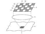
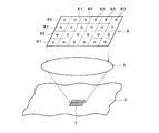
- FIG. 1 is a schematic perspective view showing a low-temperature polysilicon film forming apparatus according to a first embodiment of the present invention.
- this 1st Embodiment it is a typical expansion perspective view which shows the one micro lens and corresponding mask. It is a figure which shows the laser irradiation apparatus which uses a micro lens.
- It is a typical perspective view which shows the formation apparatus of the low-temperature polysilicon film which concerns on 2nd Embodiment of this invention.
- (A) is sectional drawing which shows the mask of the formation apparatus of the low temperature polysilicon film based on 4th Embodiment of this invention
- (b) is the top view.
- FIG. 1 is a schematic perspective view showing an apparatus for forming a low-temperature polysilicon film according to an embodiment of the present invention
- FIG. 2 is a schematic enlarged perspective view showing one microlens and a corresponding mask
- FIG. It is a figure which shows the laser irradiation apparatus using a micro lens.
- the laser irradiation apparatus shown in FIG. 3 is annealed by irradiating only the channel region formation scheduled region with laser light, for example. This is an apparatus for polycrystallizing and forming a polysilicon film.
- the laser light emitted from the light source 1 is shaped into a parallel beam by the lens group 2 and irradiated to the irradiated object 6 through the microlens array including a large number of microlenses 5.
- the laser light source 1 is, for example, an excimer laser that emits laser light having a wavelength of 308 nm or 353 nm at a repetition period of, for example, 50 Hz.
- a large number of microlenses 5 are arranged on a transparent substrate 4, and the laser light is focused on a thin film transistor formation scheduled area set on a thin film transistor substrate as an irradiated body 6.
- the transparent substrate 4 is arranged in parallel to the irradiated body 6, and the microlenses 5 are arranged at a pitch of an integer multiple (for example, 2) of 2 or more of the arrangement pitch of the transistor formation scheduled regions.
- the irradiated body 6 of the present embodiment is, for example, a thin film transistor, and a polysilicon channel region is formed by irradiating a laser beam to the channel region formation scheduled region of the a-Si film.
- a gate electrode made of a metal film such as Al is patterned on a glass substrate by sputtering.
- a gate insulating film made of a SiN film is formed on the entire surface by low temperature plasma CVD at 250 to 300 ° C. using silane and H 2 gas as source gases.
- an a-Si: H film is formed on the gate insulating film by, eg, plasma CVD.
- This a-Si: H film is formed by using a mixed gas of silane and H 2 gas as a source gas.
- one microlens 5 is arranged in each channel region, and only this channel formation planned region is irradiated with laser light and annealed. Then, this channel formation scheduled region is polycrystallized to form a polysilicon channel region.
- a light shielding member for irradiating only the channel formation scheduled region with the laser beam is disposed above the microlens 5, and the channel region is defined by the light shielding member.
- 3A and 1 only show a state in which the microlenses 5 are arranged one-dimensionally, this is for simplification of illustration, and in fact, FIG. ), The microlenses 5 are two-dimensionally arranged. However, the microlenses 5 may be arranged one-dimensionally in accordance with the arrangement of regions to be polycrystallized.
- one mask 3 is provided above each microlens 5 for each microlens 5.
- the mask 3 has a rectangular shape as a whole, and is further divided into fine rectangular grid-like regions.
- a light shielding region 31 that shields laser light and a transmission region 32 that transmits laser light are arranged in a grid so that the light shielding region 31 and the transmission region 32 are not adjacent to each other.
- an irradiation region of the laser light is formed in the a-Si: H film corresponding to the channel region formation scheduled region 7. Is done.
- the irradiation pattern of the laser light in the planned area 7 corresponds to the pattern of the transmission area 32 of the mask 3.
- the object 6 is irradiated with laser light using the mask 3.
- the parallel beam of laser light passes through the mask 3, is collected by each microlens 5, and is irradiated to the channel formation scheduled region 7 in the a-Si: H film of the irradiated body 6.
- the laser light is shielded in the light shielding region 31 of the mask 3, and only the portion that has passed through the transmission region 32 is irradiated to the planned region 7, and the laser light irradiation region has a lattice pattern similar to the mask 3. It is formed.
- the polysilicon portion is a portion in which the transmission region 32 of the mask 3 is reduced and projected by the microlens 5, and laser light is irradiated only to the reduced and projected portion. , It does not coarsen beyond this reduced projected portion. For this reason, in the polysilicon portion, the size of the crystal grain is regulated by the size of the region where the transmission region 32 is reduced and projected, and the size of the crystal grain is within a narrow crystal grain size range. Be controlled.
- the mask 3 is removed, and then the irradiated body 6 is irradiated with laser light, whereby the entire planned area 7 is irradiated with the laser light for each channel area formation planned area 7. .
- the portion that has been polycrystallized in the first step does not remelt.
- the portion corresponding to the light-shielding region 31 of the mask 3 in the a-Si: H film remains amorphous. This amorphous portion is melted and solidified by laser irradiation in the second step. To polycrystallize.
- the portion that is polycrystallized in the second step is a portion in which the light shielding region 31 in the a-Si: H film is projected in a reduced scale.
- the crystal grains do not become coarse beyond the reduced projected portion. Accordingly, the polysilicon portion formed in the second step is also controlled by the size of the region where the light-shielding region 31 is reduced and projected, and the size of the crystal grains is controlled within a certain narrow range.
- a polysilicon film in which the size of the crystal grains is controlled within a certain narrow range is formed. Therefore, a transistor using this polysilicon film as a channel region can operate at high speed, and since the crystal grains in the polysilicon channel region are uniform, a semiconductor device with stable transistor characteristics can be obtained.
- the shape of the light shielding region 31 and the transmission region 32 of the mask 4 is not limited to a rectangle, and may be various shapes such as a circle.
- the mask other than the light shielding region that defines the channel region is not used in the second step. However, the mask is used in the second step, and the light shielding is performed in the first step. The portion that was the region was used as the transmission region, and the portion that was the transmission region was used as the light-shielding region, and only the portion that remained amorphous in the first step in the a-Si: H film was irradiated with laser light and annealed. It is good to do.
- the transmission region in the second step is made smaller than the light shielding region in the first step, and a gap is formed between the laser light irradiation region in the first step and the laser light irradiation region in the second step. It may be provided.
- the amorphous region is polycrystallized in the second step, crystal growth can be prevented from starting from the polysilicon portion already polycrystallized in the first step. Thereby, the polysilicon can be grown in the second step without being affected by the crystal grain form of the polysilicon in the first step.
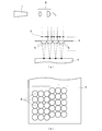
- FIG. 8 This embodiment is different from the first embodiment only in the configuration of the mask 8.
- the entire surface of the mask 8 is a light shielding region, and circular transmission regions 83 are formed in the light shielding region, for example, so as to be scattered.
- a plurality of rectangular regions 81 and 82 can be assumed. That is, in the mask 8, a plurality of regions 81 and 82 are considered, and the mask 8 is assumed to have one transmission region 83 arranged for each of these regions 81 and 82.
- this mask 8 when this mask 8 is used to irradiate the irradiated body 6 with laser light by the microlens 5, in the channel region formation scheduled area 7 of the irradiated body 6, the irradiated portions of the laser light are equally spaced in a spot shape. It will be arranged in.
- the first step laser light is irradiated to the channel region formation scheduled region 7 of the irradiated body 6 by the microlens 5 using the mask 8. Then, in the planned area 7, an irradiation pattern in which the areas irradiated with the laser beam in spots are scattered at equal intervals. The region irradiated with the laser beam in a spot shape becomes polysilicon obtained by melting and solidifying the a-Si: H film to be polycrystalline.
- the mask 8 is removed and the entire planned area 7 is irradiated with laser light. Then, crystallization occurs using the spot-like region polycrystallized in the first step as a seed, and the entire planned region 7 becomes a polysilicon film.
- the obtained polysilicon film already has a portion corresponding to the transmission region 83 for each reduced projection region of each of the regions 81 and 82 in the region where the mask 8 in the a-Si: H film is reduced and projected. The polycrystallized portion is used as a seed for crystallization.
- the size of the crystal grains is not coarsened beyond at least the reduced projection area of the regions 81 and 82, and the obtained polysilicon film was controlled in a narrow range where the size of the crystal grains was constant. It will be a thing. Therefore, even if the forming apparatus of the second embodiment is used, the same effect as that of the first embodiment is obtained.
- the entire planned area 7 is irradiated with laser light. This is because the recrystallized region does not melt even if it is irradiated again with laser light because the melting point rises, and it remains as a polycrystal.
- the laser light emission conditions that is, the conditions for heating the a-Si: H film can be the same in the first step and the second step.
- the size of the light shielding region 31 and the transmission region 32 of the mask 3 of the first embodiment, and the interval between the transmission regions 83 of the mask 8 of the second embodiment (that is, the size of the conceptual regions 81 and 82).
- one side length may be about 1 ⁇ m.
- the size of the crystal grains of the polysilicon film is equal to or less than 1 ⁇ m.
- the thin film transistor has a side length of about a few tens to several tens of ⁇ m, a sufficiently stable transistor characteristic can be obtained if the size of crystal grains in the channel polysilicon region is 1 ⁇ m or less.
- the size of the regions 81 and 82 in the second embodiment can be set to about 1 ⁇ m in terms of one side length in the region projected and reduced on the irradiation object 6.
- the size of the transmission region 83 of the mask 8 is the size when the projection is reduced and projected onto the irradiation object 6, for example, the diameter can be about 0.1 ⁇ m.
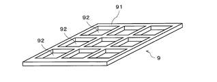
- the mask 9 in FIG. 5 has a shape in which a plurality of rectangular holes are hollowed out at a predetermined interval with respect to a light shielding member 91 formed of a material that shields laser light.
- a plurality of transmissive regions 92 made up of the two holes are two-dimensionally arranged, and these transmissive regions 92 are surrounded by the light shielding regions made up of the light shielding member 91 and partitioned by the light shielding regions.
- the mask 9 is used to irradiate the microlens 5 with a laser beam to the channel region formation scheduled region of the irradiated body 6.
- the amorphous silicon film (a-Si film) is irradiated only with the laser light transmitted through the transmission region 92 of the mask 9.
- the a-Si film only the portion corresponding to the transmission region is annealed, melted and solidified, and crystallized into polysilicon.
- the size of the crystal grain of the polysilicon portion is regulated corresponding to each transmission region 92 of the mask, and at least one crystal grain becomes coarser beyond one transmission region 92. There is nothing. For this reason, the variation in crystal grain size is small. Further, the portion corresponding to the light shielding region (light shielding member 91) of the mask remains amorphous.
- the mask 9 is removed, and the entire region where the channel is to be formed is irradiated with laser light. Then, crystallization occurs using the spot-like region polycrystallized in the first step as a seed, and the entire planned region becomes a polysilicon film.
- the obtained polysilicon film in the area where the mask 9 in the a-Si: H film is reduced and projected, there are already many portions corresponding to the transmission area 92 for each reduction projection area of each transmission area 92.
- the crystallized portion is used as a seed for crystallization. Therefore, the size of the crystal grains does not become coarser at least beyond the reduced projection area of the transmission region 92, and the obtained polysilicon film has a crystal grain size controlled within a narrow range. It becomes. Therefore, even if the forming apparatus of the third embodiment is used, the same effect as that of the first embodiment is obtained.
- the entire planned area is irradiated with laser light. This is because the recrystallized region does not melt even if it is irradiated again with laser light because the melting point rises, and it remains as a polycrystal.
- spot-like light shielding regions 12 for shielding laser light are two-dimensionally arranged at regular intervals on the lower surface of a plate-like transmission member 11 through which the mask 10 transmits laser light.
- the light shielding region 12 is formed by attaching a minute cylindrical light shielding member that shields laser light to the lower surface of the transmission member 11.
- the plurality of spot-shaped light shielding regions 12 are two-dimensionally arranged while being supported by the transmissive member 11.
- the laser light irradiation process is a single process.
- the laser light transmitted through the portion where the light shielding region 12 does not exist in the transmission member 11 is irradiated onto the a-Si film to heat and melt this portion.
- the portion of the a-Si film corresponding to the light shielding region 12 is not irradiated with the laser light and is merely heated by heat conduction from the irradiation region, so that the temperature is lower than that of the irradiation region.
- crystallization proceeds from the non-irradiation region during solidification, and the irradiation region then crystallizes. Does not occur. That is, since crystallization proceeds from the portion corresponding to each light shielding region 12 corresponding to the region divided by the thin line in FIG. 6B, the obtained polysilicon film exceeds the region divided by the thin line. As a result, the crystal grains are not coarsened, and a polysilicon film having a uniform crystal grain size can be obtained.
- the present invention is useful for manufacturing a semiconductor device having stable transistor characteristics.
Landscapes
- Engineering & Computer Science (AREA)
- Physics & Mathematics (AREA)
- Chemical & Material Sciences (AREA)
- Crystallography & Structural Chemistry (AREA)
- Manufacturing & Machinery (AREA)
- Power Engineering (AREA)
- Microelectronics & Electronic Packaging (AREA)
- Computer Hardware Design (AREA)
- Condensed Matter Physics & Semiconductors (AREA)
- General Physics & Mathematics (AREA)
- Organic Chemistry (AREA)
- Metallurgy (AREA)
- Materials Engineering (AREA)
- Optics & Photonics (AREA)
- High Energy & Nuclear Physics (AREA)
- Electromagnetism (AREA)
- Health & Medical Sciences (AREA)
- Toxicology (AREA)
- Thermal Sciences (AREA)
- Recrystallisation Techniques (AREA)
- Thin Film Transistor (AREA)
Priority Applications (2)
| Application Number | Priority Date | Filing Date | Title |
|---|---|---|---|
| CN201080050013.XA CN102714149B (zh) | 2009-11-05 | 2010-10-14 | 用于形成低温多晶硅膜的装置和方法 |
| US13/505,721 US8748326B2 (en) | 2009-11-05 | 2010-10-14 | Device and method for forming low-temperature polysilicon film |
Applications Claiming Priority (2)
| Application Number | Priority Date | Filing Date | Title |
|---|---|---|---|
| JP2009-254216 | 2009-11-05 | ||
| JP2009254216A JP5534402B2 (ja) | 2009-11-05 | 2009-11-05 | 低温ポリシリコン膜の形成装置及び方法 |
Publications (1)
| Publication Number | Publication Date |
|---|---|
| WO2011055618A1 true WO2011055618A1 (ja) | 2011-05-12 |
Family
ID=43969858
Family Applications (1)
| Application Number | Title | Priority Date | Filing Date |
|---|---|---|---|
| PCT/JP2010/068005 Ceased WO2011055618A1 (ja) | 2009-11-05 | 2010-10-14 | 低温ポリシリコン膜の形成装置及び方法 |
Country Status (6)
| Country | Link |
|---|---|
| US (1) | US8748326B2 (enExample) |
| JP (1) | JP5534402B2 (enExample) |
| KR (1) | KR101645770B1 (enExample) |
| CN (1) | CN102714149B (enExample) |
| TW (1) | TWI512833B (enExample) |
| WO (1) | WO2011055618A1 (enExample) |
Cited By (8)
| Publication number | Priority date | Publication date | Assignee | Title |
|---|---|---|---|---|
| CN102738079A (zh) * | 2012-05-31 | 2012-10-17 | 昆山工研院新型平板显示技术中心有限公司 | 多晶硅激光退火装置及其方法 |
| JP2018137302A (ja) * | 2017-02-21 | 2018-08-30 | 株式会社ブイ・テクノロジー | レーザ照射装置、薄膜トランジスタの製造方法およびプログラム |
| US10559600B2 (en) | 2018-06-28 | 2020-02-11 | Sakai Display Products Corporation | Thin film transistor, display device and method for producing thin film transistor |
| US10770483B2 (en) | 2018-06-28 | 2020-09-08 | Sakai Display Products Corporation | Thin film transistor, display device and method for manufacturing thin film transistor |
| US11081507B2 (en) | 2017-07-12 | 2021-08-03 | Sakai Display Products Corporation | Semiconductor device and method for manufacturing same |
| US11121262B2 (en) | 2017-07-12 | 2021-09-14 | Sakai Display Products Corporation | Semiconductor device including thin film transistor and method for manufacturing the same |
| US11133333B2 (en) | 2018-06-28 | 2021-09-28 | Sakai Display Products Corporation | Producing method for thin film transistor with different crystallinities |
| US11495689B2 (en) | 2018-08-08 | 2022-11-08 | Sakai Display Products Corporation | Thin-film transistor and method for producing same |
Families Citing this family (14)
| Publication number | Priority date | Publication date | Assignee | Title |
|---|---|---|---|---|
| JP5884147B2 (ja) * | 2010-12-09 | 2016-03-15 | 株式会社ブイ・テクノロジー | レーザアニール装置及びレーザアニール方法 |
| US8785815B2 (en) * | 2012-06-22 | 2014-07-22 | Applied Materials, Inc. | Aperture control of thermal processing radiation |
| DE102012110165A1 (de) * | 2012-10-24 | 2014-02-13 | Jenoptik Automatisierungstechnik Gmbh | Vorrichtung zum Verbinden zweier Werkstückteile mit Bereichen unterschiedlicher Eigenschaften mittels Durchstrahlschweißen |
| US9640423B2 (en) * | 2015-07-30 | 2017-05-02 | GlobalFoundries, Inc. | Integrated circuits and methods for their fabrication |
| KR102467402B1 (ko) * | 2015-12-15 | 2022-11-15 | 삼성디스플레이 주식회사 | 실리콘 결정화 방법 및 박막 트랜지스터 기판의 제조방법 |
| JP6781872B2 (ja) * | 2016-07-20 | 2020-11-11 | 株式会社ブイ・テクノロジー | レーザ照射装置および薄膜トランジスタの製造方法 |
| US10811286B2 (en) * | 2016-09-28 | 2020-10-20 | Sakai Display Products Corporation | Laser annealing device and laser annealing method |
| WO2018092218A1 (ja) * | 2016-11-16 | 2018-05-24 | 株式会社ブイ・テクノロジー | レーザ照射装置、薄膜トランジスタおよび薄膜トランジスタの製造方法 |
| CN107482066B (zh) * | 2017-09-20 | 2021-01-15 | 京东方科技集团股份有限公司 | 薄膜晶体管及其制备方法、阵列基板和显示装置 |
| JP2019062079A (ja) * | 2017-09-26 | 2019-04-18 | 株式会社ブイ・テクノロジー | レーザ照射装置、レーザ照射方法及び投影マスク |
| CN109742042B (zh) * | 2019-01-10 | 2020-07-31 | 京东方科技集团股份有限公司 | 低温多晶硅的激光退火装置和退火方法 |
| WO2020177056A1 (zh) * | 2019-03-04 | 2020-09-10 | 京东方科技集团股份有限公司 | 薄膜晶体管及薄膜晶体管的制造方法 |
| EP3761344A1 (en) * | 2019-07-05 | 2021-01-06 | Laser Systems & Solutions of Europe | System and method for spatially controlling an amount of energy delivered to a processed surface of a substrate |
| JP7495043B2 (ja) | 2020-01-10 | 2024-06-04 | 株式会社ブイ・テクノロジー | 多結晶膜の形成方法およびレーザ結晶化装置 |
Citations (7)
| Publication number | Priority date | Publication date | Assignee | Title |
|---|---|---|---|---|
| JP2003109911A (ja) * | 2001-10-01 | 2003-04-11 | Sharp Corp | 薄膜処理装置、薄膜処理方法および薄膜デバイス |
| JP2003203874A (ja) * | 2002-01-10 | 2003-07-18 | Sharp Corp | レーザ照射装置 |
| JP2006511064A (ja) * | 2002-08-19 | 2006-03-30 | ザ トラスティーズ オブ コロンビア ユニヴァーシティ イン ザ シティ オブ ニューヨーク | 基板上のフィルム領域をレーザ結晶化処理してほぼ均一にするプロセス及びシステム、及びこのフィルム領域の構造 |
| JP2006287129A (ja) * | 2005-04-04 | 2006-10-19 | Sumitomo Heavy Ind Ltd | レーザ照射装置、及びレーザ照射方法 |
| JP2007043127A (ja) * | 2005-08-04 | 2007-02-15 | Samsung Electronics Co Ltd | 逐次的横方向結晶化用のマスク及びその製造方法 |
| JP2008131024A (ja) * | 2006-11-27 | 2008-06-05 | Canon Inc | 近接場露光によるレジストパターンの形成方法 |
| JP2008521247A (ja) * | 2004-11-18 | 2008-06-19 | ザ トラスティーズ オブ コロンビア ユニヴァーシティ イン ザ シティ オブ ニューヨーク | 結晶方位制御ポリシリコン膜を生成するためのシステム及び方法 |
Family Cites Families (11)
| Publication number | Priority date | Publication date | Assignee | Title |
|---|---|---|---|---|
| JPH0563196A (ja) | 1991-09-04 | 1993-03-12 | Hitachi Ltd | 薄膜半導体装置及びその製造方法並び液晶表示装置 |
| US7329611B2 (en) * | 2002-04-11 | 2008-02-12 | Nec Corporation | Method for forming finely-structured parts, finely-structured parts formed thereby, and product using such finely-structured part |
| KR100920343B1 (ko) * | 2003-01-08 | 2009-10-07 | 삼성전자주식회사 | 다결정 규소 박막 트랜지스터 표시판 및 그 제조 방법 |
| KR100631013B1 (ko) * | 2003-12-29 | 2006-10-04 | 엘지.필립스 엘시디 주식회사 | 주기성을 가진 패턴이 형성된 레이저 마스크 및 이를이용한 결정화방법 |
| US7611577B2 (en) * | 2004-03-31 | 2009-11-03 | Nec Corporation | Semiconductor thin film manufacturing method and device, beam-shaping mask, and thin film transistor |
| KR100675936B1 (ko) * | 2004-08-06 | 2007-02-02 | 비오이 하이디스 테크놀로지 주식회사 | 단결정실리콘막 형성방법 |
| JP2006237270A (ja) * | 2005-02-24 | 2006-09-07 | Sony Corp | 薄膜半導体装置及びその製造方法と表示装置 |
| KR100742380B1 (ko) * | 2005-12-28 | 2007-07-24 | 삼성에스디아이 주식회사 | 마스크 패턴, 박막 트랜지스터의 제조 방법 및 이를사용하는 유기 전계 발광 표시 장치의 제조 방법 |
| JP2008147429A (ja) * | 2006-12-11 | 2008-06-26 | Sumitomo Heavy Ind Ltd | レーザアニール装置及びレーザアニール方法 |
| JP2009032952A (ja) * | 2007-07-27 | 2009-02-12 | Sharp Corp | レーザ照射装置、レーザ照射方法、結晶材料、および、機能素子 |
| KR101073551B1 (ko) * | 2009-11-16 | 2011-10-17 | 삼성모바일디스플레이주식회사 | 레이저 마스크 및 이를 이용한 순차적 측면 고상 결정화 방법 |
-
2009
- 2009-11-05 JP JP2009254216A patent/JP5534402B2/ja not_active Expired - Fee Related
-
2010
- 2010-10-14 KR KR1020127014465A patent/KR101645770B1/ko not_active Expired - Fee Related
- 2010-10-14 US US13/505,721 patent/US8748326B2/en not_active Expired - Fee Related
- 2010-10-14 CN CN201080050013.XA patent/CN102714149B/zh not_active Expired - Fee Related
- 2010-10-14 WO PCT/JP2010/068005 patent/WO2011055618A1/ja not_active Ceased
- 2010-11-01 TW TW099137462A patent/TWI512833B/zh not_active IP Right Cessation
Patent Citations (7)
| Publication number | Priority date | Publication date | Assignee | Title |
|---|---|---|---|---|
| JP2003109911A (ja) * | 2001-10-01 | 2003-04-11 | Sharp Corp | 薄膜処理装置、薄膜処理方法および薄膜デバイス |
| JP2003203874A (ja) * | 2002-01-10 | 2003-07-18 | Sharp Corp | レーザ照射装置 |
| JP2006511064A (ja) * | 2002-08-19 | 2006-03-30 | ザ トラスティーズ オブ コロンビア ユニヴァーシティ イン ザ シティ オブ ニューヨーク | 基板上のフィルム領域をレーザ結晶化処理してほぼ均一にするプロセス及びシステム、及びこのフィルム領域の構造 |
| JP2008521247A (ja) * | 2004-11-18 | 2008-06-19 | ザ トラスティーズ オブ コロンビア ユニヴァーシティ イン ザ シティ オブ ニューヨーク | 結晶方位制御ポリシリコン膜を生成するためのシステム及び方法 |
| JP2006287129A (ja) * | 2005-04-04 | 2006-10-19 | Sumitomo Heavy Ind Ltd | レーザ照射装置、及びレーザ照射方法 |
| JP2007043127A (ja) * | 2005-08-04 | 2007-02-15 | Samsung Electronics Co Ltd | 逐次的横方向結晶化用のマスク及びその製造方法 |
| JP2008131024A (ja) * | 2006-11-27 | 2008-06-05 | Canon Inc | 近接場露光によるレジストパターンの形成方法 |
Cited By (9)
| Publication number | Priority date | Publication date | Assignee | Title |
|---|---|---|---|---|
| CN102738079A (zh) * | 2012-05-31 | 2012-10-17 | 昆山工研院新型平板显示技术中心有限公司 | 多晶硅激光退火装置及其方法 |
| JP2018137302A (ja) * | 2017-02-21 | 2018-08-30 | 株式会社ブイ・テクノロジー | レーザ照射装置、薄膜トランジスタの製造方法およびプログラム |
| WO2018155455A1 (ja) * | 2017-02-21 | 2018-08-30 | 株式会社ブイ・テクノロジー | レーザ照射装置、薄膜トランジスタの製造方法、プログラムおよび投影マスク |
| US11081507B2 (en) | 2017-07-12 | 2021-08-03 | Sakai Display Products Corporation | Semiconductor device and method for manufacturing same |
| US11121262B2 (en) | 2017-07-12 | 2021-09-14 | Sakai Display Products Corporation | Semiconductor device including thin film transistor and method for manufacturing the same |
| US10559600B2 (en) | 2018-06-28 | 2020-02-11 | Sakai Display Products Corporation | Thin film transistor, display device and method for producing thin film transistor |
| US10770483B2 (en) | 2018-06-28 | 2020-09-08 | Sakai Display Products Corporation | Thin film transistor, display device and method for manufacturing thin film transistor |
| US11133333B2 (en) | 2018-06-28 | 2021-09-28 | Sakai Display Products Corporation | Producing method for thin film transistor with different crystallinities |
| US11495689B2 (en) | 2018-08-08 | 2022-11-08 | Sakai Display Products Corporation | Thin-film transistor and method for producing same |
Also Published As
| Publication number | Publication date |
|---|---|
| KR20120109496A (ko) | 2012-10-08 |
| JP5534402B2 (ja) | 2014-07-02 |
| CN102714149B (zh) | 2015-07-29 |
| TWI512833B (zh) | 2015-12-11 |
| CN102714149A (zh) | 2012-10-03 |
| US20120220140A1 (en) | 2012-08-30 |
| JP2011100838A (ja) | 2011-05-19 |
| KR101645770B1 (ko) | 2016-08-12 |
| TW201123312A (en) | 2011-07-01 |
| US8748326B2 (en) | 2014-06-10 |
Similar Documents
| Publication | Publication Date | Title |
|---|---|---|
| JP5534402B2 (ja) | 低温ポリシリコン膜の形成装置及び方法 | |
| KR100712648B1 (ko) | 반도체 박막을 결정화하는 방법, 레이저 조사 시스템, 박막 트랜지스터 제조 방법, 표시 장치의 제조 방법 및 유기 el 표시 장치의 제조 방법 | |
| JP5495043B2 (ja) | レーザアニール方法、装置及びマイクロレンズアレイ | |
| WO2011158612A1 (ja) | 低温ポリシリコン膜の形成装置及び方法 | |
| KR100492152B1 (ko) | 실리콘 결정화방법 | |
| JPH08236443A (ja) | 半導体結晶の成長方法および半導体製造装置 | |
| JP5800292B2 (ja) | レーザ処理装置 | |
| JP6221088B2 (ja) | レーザアニール装置及びレーザアニール方法 | |
| US8278163B2 (en) | Semiconductor processing apparatus and semiconductor processing method | |
| JP2006013050A (ja) | レーザビーム投影マスク及びそれを用いたレーザ加工方法、レーザ加工装置 | |
| JP4408667B2 (ja) | 薄膜半導体の製造方法 | |
| JP2008227445A (ja) | 薄膜トランジスタ及び表示装置 | |
| JP2007281465A (ja) | 多結晶膜の形成方法 | |
| WO2013030885A1 (ja) | 薄膜形成基板の製造方法及び薄膜基板 | |
| JP4763983B2 (ja) | 光変調素子、結晶化装置、結晶化方法、薄膜半導体基板の製造装置、薄膜半導体基板の製造方法、薄膜半導体装置、薄膜半導体装置の製造方法、表示装置及び位相シフタ | |
| WO2006075568A1 (ja) | 多結晶半導体薄膜の製造方法および製造装置 | |
| JP2005276944A (ja) | 半導体デバイス、その製造方法および製造装置 | |
| JP2008244374A (ja) | 半導体薄膜の製造方法、半導体薄膜及び薄膜トランジスタ | |
| KR100575235B1 (ko) | 레이저 광학계 및 이를 이용한 결정화 방법 | |
| JP2005347380A (ja) | 半導体薄膜の製造方法および製造装置 | |
| JP2007207896A (ja) | レーザビーム投影マスクおよびそれを用いたレーザ加工方法、レーザ加工装置 | |
| JP4467276B2 (ja) | 半導体薄膜を製造する方法と装置 | |
| JP2008147236A (ja) | 結晶化装置およびレーザ加工方法 | |
| JP2011139082A (ja) | 光変調素子、結晶化装置、結晶化方法、薄膜半導体基板の製造装置、薄膜半導体基板の製造方法、薄膜半導体装置、薄膜半導体装置の製造方法および表示装置 | |
| JP2008311494A (ja) | 結晶性半導体膜の製造方法、及び、レーザー装置 |
Legal Events
| Date | Code | Title | Description |
|---|---|---|---|
| WWE | Wipo information: entry into national phase |
Ref document number: 201080050013.X Country of ref document: CN |
|
| 121 | Ep: the epo has been informed by wipo that ep was designated in this application |
Ref document number: 10828178 Country of ref document: EP Kind code of ref document: A1 |
|
| WWE | Wipo information: entry into national phase |
Ref document number: 13505721 Country of ref document: US |
|
| NENP | Non-entry into the national phase |
Ref country code: DE |
|
| ENP | Entry into the national phase |
Ref document number: 20127014465 Country of ref document: KR Kind code of ref document: A |
|
| 122 | Ep: pct application non-entry in european phase |
Ref document number: 10828178 Country of ref document: EP Kind code of ref document: A1 |