WO2011016306A1 - 光学積層体、偏光板及び画像表示装置 - Google Patents
光学積層体、偏光板及び画像表示装置 Download PDFInfo
- Publication number
- WO2011016306A1 WO2011016306A1 PCT/JP2010/061327 JP2010061327W WO2011016306A1 WO 2011016306 A1 WO2011016306 A1 WO 2011016306A1 JP 2010061327 W JP2010061327 W JP 2010061327W WO 2011016306 A1 WO2011016306 A1 WO 2011016306A1
- Authority
- WO
- WIPO (PCT)
- Prior art keywords
- hard coat
- inorganic fine
- coat layer
- fine particles
- fine particle
- Prior art date
- Legal status (The legal status is an assumption and is not a legal conclusion. Google has not performed a legal analysis and makes no representation as to the accuracy of the status listed.)
- Ceased
Links
Images


Classifications
-
- G—PHYSICS
- G02—OPTICS
- G02B—OPTICAL ELEMENTS, SYSTEMS OR APPARATUS
- G02B1/00—Optical elements characterised by the material of which they are made; Optical coatings for optical elements
- G02B1/10—Optical coatings produced by application to, or surface treatment of, optical elements
- G02B1/11—Anti-reflection coatings
-
- G—PHYSICS
- G02—OPTICS
- G02B—OPTICAL ELEMENTS, SYSTEMS OR APPARATUS
- G02B1/00—Optical elements characterised by the material of which they are made; Optical coatings for optical elements
- G02B1/10—Optical coatings produced by application to, or surface treatment of, optical elements
- G02B1/14—Protective coatings, e.g. hard coatings
-
- G—PHYSICS
- G02—OPTICS
- G02B—OPTICAL ELEMENTS, SYSTEMS OR APPARATUS
- G02B5/00—Optical elements other than lenses
- G02B5/02—Diffusing elements; Afocal elements
-
- G—PHYSICS
- G02—OPTICS
- G02B—OPTICAL ELEMENTS, SYSTEMS OR APPARATUS
- G02B1/00—Optical elements characterised by the material of which they are made; Optical coatings for optical elements
- G02B1/10—Optical coatings produced by application to, or surface treatment of, optical elements
- G02B1/11—Anti-reflection coatings
- G02B1/111—Anti-reflection coatings using layers comprising organic materials
-
- G—PHYSICS
- G02—OPTICS
- G02B—OPTICAL ELEMENTS, SYSTEMS OR APPARATUS
- G02B1/00—Optical elements characterised by the material of which they are made; Optical coatings for optical elements
- G02B1/10—Optical coatings produced by application to, or surface treatment of, optical elements
- G02B1/16—Optical coatings produced by application to, or surface treatment of, optical elements having an anti-static effect, e.g. electrically conducting coatings
-
- G—PHYSICS
- G02—OPTICS
- G02B—OPTICAL ELEMENTS, SYSTEMS OR APPARATUS
- G02B5/00—Optical elements other than lenses
- G02B5/30—Polarising elements
-
- G—PHYSICS
- G02—OPTICS
- G02B—OPTICAL ELEMENTS, SYSTEMS OR APPARATUS
- G02B5/00—Optical elements other than lenses
- G02B5/30—Polarising elements
- G02B5/3025—Polarisers, i.e. arrangements capable of producing a definite output polarisation state from an unpolarised input state
- G02B5/3033—Polarisers, i.e. arrangements capable of producing a definite output polarisation state from an unpolarised input state in the form of a thin sheet or foil, e.g. Polaroid
-
- Y—GENERAL TAGGING OF NEW TECHNOLOGICAL DEVELOPMENTS; GENERAL TAGGING OF CROSS-SECTIONAL TECHNOLOGIES SPANNING OVER SEVERAL SECTIONS OF THE IPC; TECHNICAL SUBJECTS COVERED BY FORMER USPC CROSS-REFERENCE ART COLLECTIONS [XRACs] AND DIGESTS
- Y10—TECHNICAL SUBJECTS COVERED BY FORMER USPC
- Y10T—TECHNICAL SUBJECTS COVERED BY FORMER US CLASSIFICATION
- Y10T428/00—Stock material or miscellaneous articles
- Y10T428/24—Structurally defined web or sheet [e.g., overall dimension, etc.]
- Y10T428/24355—Continuous and nonuniform or irregular surface on layer or component [e.g., roofing, etc.]
-
- Y—GENERAL TAGGING OF NEW TECHNOLOGICAL DEVELOPMENTS; GENERAL TAGGING OF CROSS-SECTIONAL TECHNOLOGIES SPANNING OVER SEVERAL SECTIONS OF THE IPC; TECHNICAL SUBJECTS COVERED BY FORMER USPC CROSS-REFERENCE ART COLLECTIONS [XRACs] AND DIGESTS
- Y10—TECHNICAL SUBJECTS COVERED BY FORMER USPC
- Y10T—TECHNICAL SUBJECTS COVERED BY FORMER US CLASSIFICATION
- Y10T428/00—Stock material or miscellaneous articles
- Y10T428/24—Structurally defined web or sheet [e.g., overall dimension, etc.]
- Y10T428/24355—Continuous and nonuniform or irregular surface on layer or component [e.g., roofing, etc.]
- Y10T428/24364—Continuous and nonuniform or irregular surface on layer or component [e.g., roofing, etc.] with transparent or protective coating
-
- Y—GENERAL TAGGING OF NEW TECHNOLOGICAL DEVELOPMENTS; GENERAL TAGGING OF CROSS-SECTIONAL TECHNOLOGIES SPANNING OVER SEVERAL SECTIONS OF THE IPC; TECHNICAL SUBJECTS COVERED BY FORMER USPC CROSS-REFERENCE ART COLLECTIONS [XRACs] AND DIGESTS
- Y10—TECHNICAL SUBJECTS COVERED BY FORMER USPC
- Y10T—TECHNICAL SUBJECTS COVERED BY FORMER US CLASSIFICATION
- Y10T428/00—Stock material or miscellaneous articles
- Y10T428/24—Structurally defined web or sheet [e.g., overall dimension, etc.]
- Y10T428/24802—Discontinuous or differential coating, impregnation or bond [e.g., artwork, printing, retouched photograph, etc.]
- Y10T428/24893—Discontinuous or differential coating, impregnation or bond [e.g., artwork, printing, retouched photograph, etc.] including particulate material
-
- Y—GENERAL TAGGING OF NEW TECHNOLOGICAL DEVELOPMENTS; GENERAL TAGGING OF CROSS-SECTIONAL TECHNOLOGIES SPANNING OVER SEVERAL SECTIONS OF THE IPC; TECHNICAL SUBJECTS COVERED BY FORMER USPC CROSS-REFERENCE ART COLLECTIONS [XRACs] AND DIGESTS
- Y10—TECHNICAL SUBJECTS COVERED BY FORMER USPC
- Y10T—TECHNICAL SUBJECTS COVERED BY FORMER US CLASSIFICATION
- Y10T428/00—Stock material or miscellaneous articles
- Y10T428/24—Structurally defined web or sheet [e.g., overall dimension, etc.]
- Y10T428/24942—Structurally defined web or sheet [e.g., overall dimension, etc.] including components having same physical characteristic in differing degree
-
- Y—GENERAL TAGGING OF NEW TECHNOLOGICAL DEVELOPMENTS; GENERAL TAGGING OF CROSS-SECTIONAL TECHNOLOGIES SPANNING OVER SEVERAL SECTIONS OF THE IPC; TECHNICAL SUBJECTS COVERED BY FORMER USPC CROSS-REFERENCE ART COLLECTIONS [XRACs] AND DIGESTS
- Y10—TECHNICAL SUBJECTS COVERED BY FORMER USPC
- Y10T—TECHNICAL SUBJECTS COVERED BY FORMER US CLASSIFICATION
- Y10T428/00—Stock material or miscellaneous articles
- Y10T428/24—Structurally defined web or sheet [e.g., overall dimension, etc.]
- Y10T428/24942—Structurally defined web or sheet [e.g., overall dimension, etc.] including components having same physical characteristic in differing degree
- Y10T428/24983—Hardness
-
- Y—GENERAL TAGGING OF NEW TECHNOLOGICAL DEVELOPMENTS; GENERAL TAGGING OF CROSS-SECTIONAL TECHNOLOGIES SPANNING OVER SEVERAL SECTIONS OF THE IPC; TECHNICAL SUBJECTS COVERED BY FORMER USPC CROSS-REFERENCE ART COLLECTIONS [XRACs] AND DIGESTS
- Y10—TECHNICAL SUBJECTS COVERED BY FORMER USPC
- Y10T—TECHNICAL SUBJECTS COVERED BY FORMER US CLASSIFICATION
- Y10T428/00—Stock material or miscellaneous articles
- Y10T428/249921—Web or sheet containing structurally defined element or component
- Y10T428/249953—Composite having voids in a component [e.g., porous, cellular, etc.]
- Y10T428/249961—With gradual property change within a component
Definitions
- the present invention relates to an optical laminate, a polarizing plate, and an image display device.
- Image display devices such as cathode ray tube display (CRT), liquid crystal display (LCD), plasma display (PDP), electroluminescence display (ELD), field emission display (FED)
- CTR cathode ray tube display
- LCD liquid crystal display
- PDP plasma display
- ELD electroluminescence display
- FED field emission display
- an optical laminate composed of functional layers having various properties such as properties and antistatic properties.
- Patent Document 1 a method of forming a hard coat layer containing inorganic fine particles on a light-transmitting substrate is known (Patent Document 1).
- Patent Document 1 a method of forming a hard coat layer containing inorganic fine particles on a light-transmitting substrate is known (Patent Document 1).
- the film thickness is increased, the optical laminate is likely to curl (warp), and when the polarizing plate is produced by attaching the optical laminate to a polarizing element, it is difficult to apply a roll. there were.
- the amount of inorganic fine particles contained in the thick hard coat layer is increased, which is disadvantageous in terms of cost.
- Patent Document 2 an optical laminate having two hard coat layers is known (Patent Document 2).
- Patent Document 2 in order to impart hard coat properties by adding a small amount of inorganic fine particles, for example, when inorganic fine particles are added to the upper layer (surface side), a difference in refractive index occurs between the upper layer and the lower layer. For this reason, when a polarizing plate is formed using the optical layered body, there is a problem that interference fringes are generated and the appearance is deteriorated.
- JP-A-2-160543 Japanese Patent Laid-Open No. 5-8350
- An object of the present invention is to provide an optical laminate that is free of interference fringes and excellent in hard coat properties, antistatic properties, and antireflection properties at low cost.
- the present invention is an optical laminate having a light transmissive substrate and a hard coat layer (A) and a hard coat layer (B) in this order on one surface of the light transmissive substrate, B) has, in order from the portion in contact with the hard coat layer (A), an inorganic fine particle-free region (B1) and an inorganic fine particle-containing region (B2), and the inorganic fine particle-free region (B1)
- the boundary with the inorganic fine particle-containing region (B2) is an uneven shape, and the inorganic fine particle has a particle size smaller than a visible light wavelength.
- the inorganic fine particle-free region (B1) preferably contains the binder resin of the inorganic fine particle-containing region (B2) as a main component and has an average thickness not less than the visible light wavelength. It is preferable that the binder resin of the hard coat layer (A) and the binder resin of the hard coat layer (B) have compatibility.
- the hardness (Ha) of the hard coat layer (A), the hardness (Hb1) of the inorganic fine particle-free region (B1), and the hardness (Hb2) of the inorganic fine particle-containing region (B2) are expressed by the following formula (1). It is preferable to satisfy. Ha ⁇ Hb1 ⁇ Hb2 (1)
- the shape of the inorganic fine particles is preferably beaded.
- the inorganic fine particles are preferably conductive inorganic fine particles.
- the content of the inorganic fine particles in the hard coat layer (B) is preferably 10 to 80% by mass.
- the optical layered body of the present invention may further have a low refractive index layer on the side of the hard coat layer (B) opposite to the hard coat layer (A).
- the optical layered body of the present invention may further have an antifouling layer on the side of the hard coat layer (B) opposite to the hard coat layer (A).
- This invention is also a polarizing plate which has a polarizing element, Comprising: The said polarizing plate equips the surface of the said polarizing element with the above-mentioned optical laminated body, It is also a polarizing plate characterized by the above-mentioned.
- the present invention is also an image display device including the above-described optical laminate or the above-described polarizing plate on the outermost surface. The present invention is described in detail below.
- FIG. 1 is a schematic view of a cross section of the optical layered body of the present invention.
- the optical layered body of the present invention has a light-transmitting substrate 1, a hard coat layer (A) 2 and a hard coat layer (B) 3 on one surface of the light-transmitting substrate 1.
- the hard coat layer (B) 3 has an inorganic fine particle non-containing region (B1) 4 and an inorganic fine particle containing region (B2) 5 in order.
- the hard coat layer (B) 3 has an inorganic fine particle-free region (B1) 4 and an inorganic fine particle-containing region (B2) 5 in a specific layer configuration.
- the inorganic fine particle-containing region (B2) 5, the inorganic fine particle non-containing region (B1) 4 and the hard coat layer (A) 2 are layers having different hardnesses. Becomes a so-called buffer layer, and by combining this buffer layer and a layer having high hardness, an optical laminate having more excellent hard coat properties can be obtained.
- the boundary between the inorganic fine particle-free region (B1) 4 and the inorganic fine particle-containing region (B2) 5 is an uneven shape. For this reason, even if there is a difference in refractive index between the inorganic fine particle-free region (B1) 4 and the inorganic fine particle-containing region (B2) 5, the interference pattern does not occur due to the presence of the uneven shape. Furthermore, even when interference fringes are generated at the interface between the hard coat layer (A) 2 and the light-transmitting substrate 1 and / or the inorganic fine particle-free region (B1) 4, the diffusion due to the uneven shape causes the above-mentioned Interference fringes can be reduced, and an optical laminate having a good appearance can be obtained.
- the above “the boundary between the inorganic fine particle-free region (B1) 4 and the inorganic fine particle-containing region (B2) 5 is an uneven shape” means that the optical layered body of the present invention has a thickness.
- the cross section in the vertical direction it means that an uneven shape is observed at the boundary between the inorganic fine particle-free region (B1) 4 and the inorganic fine particle-containing region (B2) 5.
- the optical layered body of the present invention may cause an interface between the light transmissive substrate 1 and the hard coat layer (A) 2 and between the hard coat layer (A) 2 and the hard coat layer (B) 3.
- An interface occurs when there is no physical or chemical affinity between layers.
- the refractive index difference of each layer has a great influence, which may cause interference fringes and poor appearance.
- the optical layered body of the present invention can reduce interference fringes because of the above-described uneven shape, and the appearance is good.
- corrugated shape is formed by the presence or absence of inorganic fine particles, and there is no clear interface between the inorganic fine particle non-containing region (B1) 4 and the inorganic fine particle containing region (B2) 5.
- the concave portion has a region where inorganic fine particles are dispersed in the binder resin, and the convex portion is made only of the binder resin and no inorganic fine particles are present. Because of such an uneven shape, problems such as stray light due to the presence of the interface do not occur, and a more preferable optical laminate can be obtained.
- the said boundary is based on the presence or absence of inorganic fine particles, when the cross section of the hard coat layer (B) 3 is observed, the boundary is a mixture of punctiform and linear, or punctiform, and a complete line It does not become a shape (interface).
- the hard coat layer is divided into two layers, and inorganic fine particles are contained only in the inorganic fine particle-containing region (B2) 5. That is, in the present invention, the above-mentioned inorganic fine particles are contained at a minimum in necessary places, which is advantageous in terms of cost.
- the optical layered body of the present invention has a light transmissive substrate.
- a substrate having smoothness and heat resistance and excellent in mechanical strength is preferable.
- Specific examples of the material forming the light-transmitting substrate include polyethylene terephthalate (PET), polyethylene naphthalate, polybutylene terephthalate, polybutylene naphthalate, triacetyl cellulose (TAC), cellulose diacetate, and cellulose acetate butyrate.
- Polyamide Polyamide, polyimide, polyether sulfone, polysulfone, polypropylene (PP), cycloolefin polymer (COP), cycloolefin copolymer (COC), polymethylpentene, polyvinyl chloride, polyvinyl acetal, polyether ketone, polymethyl methacrylate , Polycarbonate, or a thermoplastic resin such as polyurethane.
- polyethylene terephthalate or triacetyl cellulose can be used.
- the thickness of the light transmissive substrate is preferably 20 to 300 ⁇ m, more preferably the lower limit is 30 ⁇ m and the upper limit is 200 ⁇ m.
- paints such as anchor agents or primers are used. Application may be performed in advance.
- the optical layered body of the present invention has a hard coat layer (A) on the light transmissive substrate.
- a transparent resin is preferable.
- an ionizing radiation curable resin an ionizing radiation curable resin which is a resin curable by ultraviolet rays or an electron beam, and solvent drying.
- examples thereof include a mixture with a mold resin (a thermoplastic resin or the like, which is a resin that forms a film only by drying a solvent added to adjust the solid content during coating), or a thermosetting resin. More preferred is an ionizing radiation curable resin.
- “resin” is a concept including resin components such as monomers and oligomers.
- Examples of the ionizing radiation curable resin include compounds having one or more unsaturated bonds such as a compound having an acrylate functional group.
- Examples of the compound having one unsaturated bond include ethyl (meth) acrylate, ethylhexyl (meth) acrylate, styrene, methylstyrene, N-vinylpyrrolidone and the like.
- Examples of the compound having two or more unsaturated bonds include polymethylolpropane tri (meth) acrylate, hexanediol (meth) acrylate, tripropylene glycol di (meth) acrylate, diethylene glycol di (meth) acrylate, pentaerythritol tri ( Polyfunctional compounds such as (meth) acrylate, dipentaerythritol hexa (meth) acrylate, 1,6-hexanediol di (meth) acrylate, neopentyl glycol di (meth) acrylate, and the above polyfunctional compound and (meth) acrylate And the like (for example, poly (meth) acrylate ester of polyhydric alcohol) and the like.
- (meth) acrylate refers to methacrylate and acrylate.
- ionizing radiation curable resin relatively low molecular weight polyester resin having unsaturated double bond, polyether resin, acrylic resin, epoxy resin, urethane resin, alkyd resin, spiroacetal resin, polybutadiene resin, polythiol polyene. Resins can also be used.
- the ionizing radiation curable resin can be used in combination with a solvent-drying resin.
- a solvent-drying resin By using the solvent-drying resin in combination, it is possible to effectively prevent coating defects on the coated surface, thereby obtaining a more excellent glossy blackness.
- the solvent-drying resin that can be used in combination with the ionizing radiation curable resin is not particularly limited, and a thermoplastic resin can be generally used.
- the thermoplastic resin is not particularly limited.
- the thermoplastic resin is preferably amorphous and soluble in an organic solvent (particularly a common solvent capable of dissolving a plurality of polymers and curable compounds).
- styrene resins, (meth) acrylic resins, alicyclic olefin resins, polyester resins, cellulose derivatives (cellulose esters, etc.) are preferable from the viewpoint of excellent film forming properties, transparency and weather resistance. .
- the material of the light transmissive substrate is a cellulose resin such as triacetyl cellulose (TAC)
- a preferred specific example of the thermoplastic resin is a cellulose resin such as nitrocellulose
- examples thereof include cellulose derivatives such as acetyl cellulose, cellulose acetate propionate, ethyl hydroxyethyl cellulose, acetyl butyl cellulose, ethyl cellulose, and methyl cellulose.
- cellulose resin vinyl acetate and copolymers thereof, vinyl chloride and copolymers thereof, vinyl resins such as vinylidene chloride and copolymers thereof, acetal resins such as polyvinyl formal and polyvinyl butyral
- thermosetting resin examples include phenol resin, urea resin, diallyl phthalate resin, melamine resin, guanamine resin, unsaturated polyester resin, polyurethane resin, epoxy resin, aminoalkyd resin, melamine-urea cocondensation resin, silicon resin, poly resin Examples thereof include siloxane resins.
- the hard coat layer (A) may contain other components as needed in addition to the binder resin.
- the other components include a photopolymerization initiator, a leveling agent, a crosslinking agent, a curing agent, a polymerization accelerator, an ultraviolet absorber, an impact absorber, a viscosity modifier, and an organic antistatic agent.
- the hard coat layer (A) can be formed using a composition for the hard coat layer (A) prepared by uniformly mixing the binder resin, other components and a solvent. The mixing may be performed using a known apparatus such as a paint shaker, a bead mill, or a kneader.
- solvent examples include water, alcohol (eg, methanol, ethanol, propanol, isopropanol, n-butanol, s-butanol, t-butanol, benzyl alcohol, PGME), ketone (eg, acetone, methyl ethyl ketone, methyl isobutyl ketone, cyclohexane).
- alcohol eg, methanol, ethanol, propanol, isopropanol, n-butanol, s-butanol, t-butanol, benzyl alcohol, PGME
- ketone eg, acetone, methyl ethyl ketone, methyl isobutyl ketone, cyclohexane.
- the solvent used in the hard coat layer (A) composition is preferably a permeable solvent.
- the above penetrating solvent is a solvent capable of expressing wettability and swelling with respect to a light-transmitting substrate on which a composition containing the solvent is applied, and further penetrates into the light-transmitting substrate. Solvent that can be used.
- the permeable solvent By using the permeable solvent, the interface between the light-transmitting substrate and the hard coat layer (A) can be substantially eliminated, so that the interlayer adhesion is good and the generation of interference fringes is prevented. Can do.
- the permeable solvent includes ketones such as acetone, methyl ethyl ketone, cyclohexanone, methyl isobutyl ketone, and diacetone alcohol; methyl formate, Esters such as methyl acetate, ethyl acetate, butyl acetate and ethyl lactate; nitrogen-containing compounds such as nitromethane, acetonitrile, N-methylpyrrolidone and N, N-dimethylformamide; glycols such as methyl glycol and methyl glycol acetate; tetrahydrofuran; Ethers such as 1,4-dioxane, dioxolane, diisopropyl ether; halogenated hydrocarbons such as methylene chloride, chloroform, tetrachloroethane; methyl cellosolve, ethyl cello
- ketones such as acetone, methyl ethyl ketone, cyclohex
- At least one selected from the group consisting of methyl acetate, ethyl acetate, butyl acetate, methyl ethyl ketone, methyl isobutyl ketone and cyclohexanone is preferable.
- the formation method of the said hard-coat layer (A) is good to follow a well-known method.
- the hard coat layer (A) composition may be applied on the light transmissive substrate to form a coating, and may be dried as necessary, and then the coating may be cured.
- the method for forming the coating film by coating include spin coating, dipping, spraying, die coating, bar coating, roll coater, meniscus coater, flexographic printing, screen printing, and bead coater. And various known methods.
- the composition is of an ultraviolet curable type, it may be cured by irradiating the film with ultraviolet rays.
- the hard coat layer (A) preferably has a thickness of 1 to 10 ⁇ m. If the thickness is less than 1 ⁇ m, the hard coat property of the optical laminate of the present invention may be insufficient. When the thickness exceeds 10 ⁇ m, curling is so strong that it may be difficult to form a polarizing plate.
- the thickness is more preferably 2 to 8 ⁇ m. The thickness is a value measured by observing a cross section of the optical layered body with an electron microscope (SEM, TEM, STEM).
- the optical layered body of the present invention has a hard coat layer (B) on the hard coat layer (A).
- the hard coat layer (B) has an inorganic fine particle-free region (B1) and an inorganic fine particle-containing region (B2) in order from the portion in contact with the hard coat layer (A).
- the inorganic fine particle-containing region (B2) containing inorganic fine particles is located on the surface side (the side opposite to the light-transmitting substrate), the hardness is high and the hard coat property is excellent.
- the inorganic fine particle non-containing region (B1) that does not contain the inorganic fine particles becomes a region having a lower hardness than the inorganic fine particle containing region (B2), and becomes a so-called buffer region, and the optical laminate is curled (warped).
- the hard coat property can be further improved by buffering the force applied from the outside to the optical layered body.
- the boundary between the inorganic fine particle-free region (B1) and the inorganic fine particle-containing region (B2) is an uneven shape.
- the inorganic fine particle non-containing region (B1) is a layer located between the hard coat layer (A) and the inorganic fine particle containing region (B2).
- the inorganic fine particle non-containing region (B1) is a layer not containing inorganic fine particles.
- the desired effect of the present invention can be obtained by adopting a specific configuration having the inorganic fine particle-free region (B1) not containing inorganic fine particles and the inorganic fine particle-containing region (B2) containing inorganic fine particles described later.
- the inorganic fine particle non-containing region (B1) is preferably composed mainly of the binder resin of the inorganic fine particle containing region (B2).
- the inorganic fine particle non-containing region (B1) preferably has an average thickness not less than the visible light wavelength. If the average thickness is less than the visible light wavelength, the interference fringes may not be suppressed. Specifically, the average thickness of the inorganic fine particle non-containing region (B1) is preferably 500 nm or more. If it is less than 500 nm, the interference fringes may not be suppressed. In the inorganic fine particle non-containing region (B1), a concavo-convex shape is formed depending on the presence or absence of the inorganic fine particles contained in the inorganic fine particle containing region (B2).
- the average thickness of the inorganic fine particle-free region (B1) means that the cross section in the thickness direction of the optical laminate is observed with an electron microscope (SEM, TEM, STEM), and the hard coat layer (A) and the hard coat layer (A) are hardened. It means an average value of values obtained by measuring the distance between the interface with the coat layer (B) and the peak of the convex portion or the bottom of the concave portion within a certain range.
- the concavo-convex shape is preferably a concavo-convex shape in which the interval between the convex portions is not less than the visible light wavelength. This is because, when the interval between the convex portions is equal to or greater than the visible light wavelength, the light incident on the concave-convex portion is appropriately scattered, and interference fringes can be prevented.
- the inorganic fine particle-containing region (B2) includes inorganic fine particles.
- the inorganic fine particle-containing region (B2) containing the inorganic fine particles has higher hardness than the inorganic fine particle-free region (B1) and the hard coat layer (A).
- By positioning such an inorganic fine particle-containing region (B2) on the surface layer side the hardness of the surface of the optical layered body can be increased and the scratch resistance can be increased.
- the optical laminated body of this invention will combine the layer from which hardness differs, it can be set as the thing excellent in hard-coat property.
- the inorganic fine particles have a particle size smaller than the visible light wavelength. This is because when the particle size of the inorganic fine particles is not less than the visible light wavelength, the transparency is lowered.
- the average primary particle diameter of the inorganic fine particles is more preferably 1 to 200 nm. If it is less than 1 nm, the hardness may not be obtained. If it exceeds 200 nm, the haze value may increase.
- the average primary particle size is more preferably 5 to 150 nm.
- the said average primary particle diameter is a value obtained by observing and measuring the cross section of the optical laminated body of this invention with an electron microscope (SEM, TEM, STEM).
- the inorganic fine particles may have a high refractive index. preferable. This is because when a low refractive index layer described later is formed, a sufficient difference in refractive index from the low refractive index layer can be obtained, and the antireflection effect of the low refractive index layer can be further exhibited.
- the inorganic fine particles have a refractive index higher than that of the binder resin. Is preferably low. This is because even if a low refractive index layer is not separately provided, the optical reflectance can be obtained with low surface reflectance and good visibility. Moreover, it is preferable to have a refractive index difference between the inorganic fine particles and the binder resin regardless of the presence or absence of the low refractive index antireflection layer described above.
- a refractive index difference occurs between the inorganic fine particle-containing region (B2) and the inorganic fine particle-free region (B1), and the light-transmitting substrate and / or inorganic fine particle-free region (B1) and the hard coat layer (A) This is because interference spots generated at the interface of the film can be reduced.
- the inorganic fine particles may be appropriately selected from those having an appropriate refractive index in accordance with the desired aspect described above, but it is usually preferable that the refractive index is 1.2 to 3.5.
- the hard coat layer (B) can have a low refractive index. Therefore, an optical laminate having good visibility can be obtained without providing a separate low refractive index layer. Can be obtained.
- the refractive index of the inorganic fine particles is preferably 1.5 to 3.5 in order to obtain a higher level of antireflection effect.
- the inorganic fine particles are not particularly limited as long as they can provide sufficient hardness to the inorganic fine particle-containing region (B2), and known inorganic fine particles can be used.
- the inorganic fine particles are preferably conductive inorganic fine particles. This is because the optical laminate of the present invention can be imparted with antistatic properties.
- the inorganic fine particles include SiO 2 (refractive index 1.20 to 1.45: including all forms such as porous and hollow), MgF (refractive index 1.38), ZnO (refractive index 1). .90, hereinafter, all values in parentheses indicate refractive index.), Sb 2 O 2 (1.71), SnO 2 (1.997), CeO 2 (1.95), indium tin oxide (Abbreviated to ITO; 1.95), In 2 O 3 (2.00), Al 2 O 3 (1.63 to 1.76), antimony-doped tin oxide (abbreviated to ATO; 2.0), aluminum-doped zinc oxide (Abbreviation: AZO; 2.0), TiO 2 (rutile type: 2.71), and the like.
- ATO or SnO 2 is preferred when it is desired to impart antistatic properties, refractive index and hardness to the optical laminate.
- the inorganic fine particles may be monodispersed, but more preferably beaded.
- the hard coat property and the above-described antistatic property can be suitably imparted with a small amount of addition, and there is no possibility of reducing the light transmittance of the optical laminate.
- the inorganic fine particles are beaded, the inorganic fine particle-free region (B1) and the inorganic fine particle-containing region (B2) can be suitably formed in the hard coat layer (B). This will be described later.
- the bead shape refers to a state where 3 to 100 inorganic fine particles are connected, and the connected state may be linear or branched.
- the inorganic fine particles may be subjected to organic treatment.
- organic treatment when an organic treatment having a reactive group is performed, it is preferable that the hard coat performance is improved by reacting with the binder resin and crosslinking.
- the organic treatment include a method in which a compound is chemically bonded to the surface of the inorganic fine particles, or a method that allows the voids in the composition forming the inorganic fine particles to penetrate without chemically bonding to the surface of the inorganic fine particles.
- the physical method is mentioned, and either method may be used.
- a chemical treatment method using an active group on a silica surface such as a hydroxyl group or a silanol group is preferably used from the viewpoint of treatment efficiency.
- a silane-based, siloxane-based, or silazane-based material having high reactivity with the above-described active group is used.
- linear alkyl single group substituted silicone materials such as methyltrichlorosilane, branched alkyl monosubstituted silicone materials, or polysubstituted linear alkyl silicone compounds such as di-n-butyldichlorosilane and ethyldimethylchlorosilane, and polysubstituted branched A chain alkyl silicone compound.
- mono-substituted, poly-substituted siloxane materials and silazane materials having a linear alkyl group or a branched alkyl group can also be used effectively.
- those having a hetero atom, an unsaturated bond group, a cyclic bond group, an aromatic functional group or the like at the terminal or intermediate part of the alkyl chain may be used.
- the content of the inorganic fine particles is preferably 10 to 80% by mass in the hard coat layer (B). If it is less than 10% by mass, the hard coat property of the optical laminate of the present invention may be inferior. When it exceeds 80 mass%, there exists a possibility of the fall of the transparency of an inorganic fine particle content layer, and the fall of hardness.
- the content is more preferably 15 to 60% by mass.
- the hard coat layer (B) having the inorganic fine particle-free region (B1) and the inorganic fine particle-containing region (B2) is formed using a composition for a hard coat layer (B) containing a binder resin and the inorganic fine particles.
- a binder resin for forming the hard coat layer (B) include the same resins as the binder resin for forming the hard coat layer (A) described above.
- a binder resin for forming the said hard-coat layer (B) it is preferable that it is resin compatible with the binder resin of the said hard-coat layer (A).
- the same resin as the binder resin of the hard coat layer (A) because the adhesion is improved and the interface that causes interference fringes becomes inconspicuous.
- the binder resin of the hard coat layer (B) and the binder resin of the hard coat layer (A) are the same, the hardness of the inorganic fine particle non-containing region (B1) is the hard coat layer (A).
- the inorganic fine particle-free region (B1) and the hard coat layer (A) both function as a buffer region, and an optical laminate having more excellent hard coat properties can be obtained. .
- the composition for the hard coat layer (B) is prepared by mixing the binder resin for forming the hard coat layer (B), the inorganic fine particles, and, if necessary, other components with a solvent. Can do.
- the other component and solvent the other component and solvent which can be used for the composition for hard-coat layers (A) mentioned above can be mentioned.
- an organic antistatic agent may be added together with the inorganic conductive fine particles. Examples of the method of mixing and preparing include the same method as the method of preparing the composition for the hard coat layer (A) described above.
- the hard coat layer (B) for example, applies a shearing force to the hard coat layer (B) composition on the hard coat layer (A) so that the web speed and the coating speed are different. It can be formed by applying and forming a film, followed by drying and curing.
- the inorganic fine particles are uniformly dispersed.
- the inorganic fine particles are separated so that the boundary between the inorganic fine particle-free region (B1) and the inorganic fine particle-containing region (B2) has an uneven shape.
- the inorganic fine particles move from the vicinity of the interface on the hard coat layer (A) side toward the opposite interface due to the shear stress acting between the hard coat layer (A) in the coating.
- the hard coat layer (B) having the inorganic fine particle non-containing region (B1) and the inorganic fine particle containing region (B2) can be formed by drying and curing the coating in such a state.
- region (B1) to form can be controlled by adjusting the composition of the said composition for hard-coat layers (B), a coating speed, a drying method, etc.
- the hard coat layer (B) composition is applied on a substrate having releasability, and the inorganic fine particles in the coating liquid are applied.
- the coating is cured.
- a hard coat layer (B) forming a hard coat layer (A) thereon, and transferring the surface of the hard coat layer (A) to the substrate.
- the hard coat layer (B) is cured, it is preferable that the hard coat layer (B) is semi-cured, because the adhesion with the hard coat layer (A) can be improved and the interface between the hard coats can be hardly generated.
- the method for applying the composition for the hard coat layer (B) is not particularly limited as long as it is a method capable of applying a certain shearing force to the film, and the method for applying the hard coat layer (A) described above is applied. The same method can be mentioned.
- the coating amount is preferably 1.5 to 15 g / cm 2 .
- a general drying method is used, and specifically, it is performed by blowing or retaining hot air of 40 to 150 ° C. for a predetermined time.
- Examples of the method for curing the coating film include the same method as the above-described curing method for the hard coat layer (A).
- the hard coat layer (B) preferably has a thickness of 1 to 10 ⁇ m. If the thickness is less than 1 ⁇ m, the hard coat property may be insufficient. When the thickness exceeds 10 ⁇ m, curling is so strong that it may be difficult to form a polarizing plate.
- the thickness is more preferably 2 to 8 ⁇ m. The thickness is a value measured by observing a cross section of the optical layered body with an electron microscope (SEM, TEM, STEM).
- the hardness (Ha) of the hard coat layer (A), the hardness (Hb1) of the inorganic fine particle-free region (B1), and the hardness (Hb2) of the inorganic fine particle-containing region (B2). ) Preferably satisfies the following formula (1).
- the optical laminate has an appropriate hardness and can prevent deformation such as curling.
- region is used.
- it can be measured by a surface film property tester (Picodenter HM500) manufactured by H. Fischer.
- the optical laminate preferably further has a low refractive index layer.
- a low refractive index layer By forming the low refractive index layer, an optical laminate having excellent antireflection properties can be obtained.
- the low refractive index layer preferably has a lower refractive index than the hard coat layers (A) and (B).
- the hard coat layers (A) and (B) preferably have a refractive index of 1.5 or more, and the low refractive index layer has a refractive index of less than 1.5.
- the refractive index of the low refractive index layer is more preferably 1.45 or less, and still more preferably 1.35 or less.
- the low refractive index layer includes 1) a resin containing silica or magnesium fluoride, 2) a fluorine-based material that is a low-refractive index resin, 3) a fluorine-containing material containing silica or magnesium fluoride, 4) silica or fluorine. You may be comprised with either of the thin films of magnesium halide.
- the fluorine-based material is a polymerizable compound containing a fluorine atom in at least a molecule or a polymer thereof.
- a polymeric compound for example, it has hardening reactive groups, such as a functional group (ionizing radiation curable group) hardened
- a functional group ionizing radiation curable group
- a polar group thermosetting polar group
- fluorine-containing monomers having an ethylenically unsaturated bond can be widely used. More specifically, fluoroolefins (eg, fluoroethylene, vinylidene fluoride, tetrafluoroethylene, hexafluoropropylene, perfluorobutadiene, perfluoro-2,2-dimethyl-1,3-dioxole, etc.) are exemplified. Can do.
- fluoroolefins eg, fluoroethylene, vinylidene fluoride, tetrafluoroethylene, hexafluoropropylene, perfluorobutadiene, perfluoro-2,2-dimethyl-1,3-dioxole, etc.
- thermosetting polar group containing a fluorine atom examples include 4-fluoroethylene-perfluoroalkyl vinyl ether copolymer; fluoroethylene-hydrocarbon vinyl ether copolymer; epoxy, polyurethane, cellulose, Examples include fluorine-modified products of resins such as phenol and polyimide.
- thermosetting polar group hydrogen bond forming groups, such as a hydroxyl group, a carboxyl group, an amino group, an epoxy group, are mentioned preferably, for example. These are excellent not only in adhesion to the coating film but also in affinity with inorganic ultrafine particles such as silica.
- Polymerizable compounds having both ionizing radiation curable groups and thermosetting polar groups include acrylic or methacrylic acid moieties and fully fluorinated alkyl, alkenyl, aryl esters, fully or partially fluorinated vinyl ethers. Examples thereof include fully or partially fluorinated vinyl esters, fully or partially fluorinated vinyl ketones, and the like.
- Examples of the polymer of the polymerizable compound containing a fluorine atom include a polymer of a monomer or a monomer mixture containing at least one fluorine-containing (meth) acrylate compound of the polymerizable compound having the ionizing radiation curable group; At least one fluorine (meth) acrylate compound and a fluorine atom in a molecule such as methyl (meth) acrylate, ethyl (meth) acrylate, propyl (meth) acrylate, butyl (meth) acrylate, 2-ethylhexyl (meth) acrylate Copolymers with (meth) acrylate compounds containing no; fluoroethylene, vinylidene fluoride, trifluoroethylene, chlorotrifluoroethylene, 3,3,3-trifluoropropylene, 1,1,2-trichloro-3, 3,3-trifluoropropylene, hex Homopolymers and copolymers of
- silicone containing vinylidene fluoride copolymer which made these copolymers contain a silicone component can also be used as a polymer of the said polymeric compound.
- silicone components in this case include (poly) dimethylsiloxane, (poly) diethylsiloxane, (poly) diphenylsiloxane, (poly) methylphenylsiloxane, alkyl-modified (poly) dimethylsiloxane, azo group-containing (poly) dimethylsiloxane, , Dimethyl silicone, phenylmethyl silicone, alkyl aralkyl modified silicone, fluorosilicone, polyether modified silicone, fatty acid ester modified silicone, methyl hydrogen silicone, silanol group containing silicone, alkoxy group containing silicone, phenol group containing silicone, methacryl modified silicone, Acrylic modified silicone, amino modified silicone, carboxylic acid modified silicone, carbinol modified silicone, epoxy modified silicone, mercapto modified silicone
- a fluorine-containing compound having at least one isocyanato group in the molecule and a compound having at least one functional group in the molecule that reacts with an isocyanato group such as an amino group, a hydroxyl group, or a carboxyl group
- an isocyanato group such as an amino group, a hydroxyl group, or a carboxyl group
- Compounds; etc. can also be used as the fluororesin.
- the low refractive index layer for example, it can be formed using a composition containing a raw material component (a composition for a refractive index layer). More specifically, a raw material component (resin, etc.) and, if necessary, an additive (for example, “fine particles having voids”, a polymerization initiator, an antistatic agent, an antifouling agent, an antiglare agent, etc., which will be described later) are solvents.
- a low refractive index layer can be obtained by using a solution or dispersion obtained by dissolving or dispersing in as a composition for a low refractive index layer, forming a coating film from the composition, and curing the coating film. .
- additives such as a polymerization initiator, an antistatic agent, antifouling agent, and an anti-glare agent.
- antistatic performance can be provided by adding an organic antistatic agent.
- the solvent similar to the solvent which can be used in formation of the above-mentioned hard-coat layer (A) can be mentioned.
- MIBK methyl isobutyl ketone
- MEK methyl ethyl ketone
- IPA isopropyl alcohol
- PGME propylene glycol monomethyl ether
- PGMEA propylene glycol monomethyl ether acetate
- the preparation method of the said composition should just be implemented according to a well-known method, if a component can be mixed uniformly. For example, it can be mixed and dispersed using the known apparatus described above in the formation of the hard coat layer.
- the low refractive index layer may be formed by a known method. For example, the various methods described above in forming the hard coat layer can be used.
- the low refractive index layer it is preferable to use “fine particles having voids” as the low refractive index agent.
- the “fine particles having voids” can lower the refractive index while maintaining the layer strength of the low refractive index layer.
- the term “fine particles having voids” refers to a structure in which fine particles are filled with gas and / or a porous structure containing gas, and the gas in the fine particles is compared with the original refractive index of the fine particles. It means fine particles whose refractive index decreases in inverse proportion to the occupation ratio.
- the present invention also includes fine particles capable of forming a nanoporous structure inside and / or at least part of the surface depending on the form, structure, aggregated state, and dispersed state of the fine particles inside the coating. .
- the low refractive index layer using these fine particles can adjust the refractive index to 1.25 to 1.45.
- Examples of the inorganic fine particles having voids include silica fine particles prepared by the method described in JP-A-2001-233611. Further, silica fine particles obtained by the production methods described in JP-A-7-133105, JP-A-2002-79616, JP-A-2006-106714 and the like may be used. Since silica fine particles having voids are easy to produce and have high hardness, when a low refractive index layer is formed by mixing with a binder, the layer strength is improved and the refractive index is 1.20-1. It is possible to adjust within a range of about 45. In particular, as specific examples of the organic fine particles having voids, hollow polymer fine particles prepared by using the technique disclosed in JP-A-2002-80503 are preferably exemplified.
- the fine particles capable of forming a nanoporous structure inside and / or at least a part of the surface of the coating are manufactured for the purpose of increasing the specific surface area in addition to the silica fine particles, and the packing column and the porous surface Examples include a release material that adsorbs various chemical substances on the part, a porous fine particle used for catalyst fixation, a dispersion or aggregate of hollow fine particles intended to be incorporated into a heat insulating material or a low dielectric material.
- an assembly of porous silica fine particles from the product names Nippil and Nipgel manufactured by Nippon Silica Kogyo Co., Ltd., and a structure in which silica fine particles manufactured by Nissan Chemical Industries, Ltd. are connected in a chain form. From the colloidal silica UP series (trade name), it is possible to use those within the preferred particle diameter range of the present invention.
- the average particle diameter of the “fine particles having voids” is preferably 5 nm to 300 nm, the lower limit is 5 nm, the upper limit is more preferably 100 nm, the lower limit is 10 nm, and the upper limit is 80 nm. preferable. When the average particle diameter of the fine particles is within this range, excellent transparency can be imparted to the low refractive index layer.
- the average particle diameter is a value measured by a dynamic light scattering method.
- the “fine particles having voids” are usually about 0.1 to 500 parts by weight, preferably about 10 to 200 parts by weight with respect to 100 parts by weight of the matrix resin in the low refractive index layer.
- the viscosity of the low refractive index layer composition is preferably in the range of 0.5 to 5 cps (25 ° C.), and more preferably 0.7, at which preferable coating properties can be obtained. ⁇ 3 cps (25 ° C).
- the resin curing means may be the same as the method described for the hard coat layer.
- a light irradiation means for the curing treatment, for example, a photopolymerization initiator that generates a radical and initiates polymerization of the polymerizable compound by light irradiation may be added to the fluororesin composition. preferable.
- the low refractive index layer has the following formula (II): 120 ⁇ n A d A ⁇ 145 (II) It is preferable from the viewpoint of low reflectivity.
- the optical layered body may have other arbitrary layers in addition to the light transmissive substrate, the hard coat layers (A) and (B), and the low refractive index layer described above.
- the optional layer include an antiglare layer, an antifouling layer, a high refractive index layer, a medium refractive index layer, and an antistatic layer.
- These layers may be formed by a known method by mixing a known anti-glare agent, a low refractive index agent, a high refractive index agent, an antistatic agent, an antifouling agent and the like with a resin and a solvent. Among these, it is preferable to further form an antifouling layer.
- the optical layered body of the present invention preferably has a hardness of 2H to 5H in a pencil hardness test (load 4.9 N) according to JIS K5600-5-4 (1999).
- the optical layered body of the present invention preferably has a surface resistance value of 10 11 ⁇ / ⁇ or less. If it exceeds 10 11 ⁇ / ⁇ , the intended antistatic performance may not be exhibited.
- the surface resistance value is more preferably 10 9 ⁇ / ⁇ or less.
- the surface resistance value can be measured with a surface resistance value measuring instrument (manufactured by Mitsubishi Chemical Corporation, product number: Hiresta IP MCP-HT260).
- the optical layered body of the present invention preferably has a total light transmittance of 80% or more. If it is less than 80%, color reproducibility and visibility may be impaired when it is mounted on the display surface.
- the total light transmittance is more preferably 85% or more, and still more preferably 90% or more.
- the total light transmittance can be measured by a method based on JIS K-7361 using a haze meter (manufactured by Murakami Color Research Laboratory, product number: HM-150).
- the hard coat layer (B) is replaced with the hard coat layer (A).
- the method of forming above is mentioned.
- the method for forming the hard coat layer (A) and the method for forming the hard coat layer (B) are as described above.
- the optical layered body of the present invention is a polarizing plate by providing on the surface of the polarizing element the surface of the optical layered body opposite to the surface on which the hard coat layer of the light-transmitting substrate is present. Can do.
- a polarizing plate is also one aspect of the present invention.
- the polarizing element is not particularly limited, and for example, a polyvinyl alcohol film, a polyvinyl formal film, a polyvinyl acetal film, an ethylene-vinyl acetate copolymer saponified film dyed with iodine or the like and stretched can be used.
- a polyvinyl alcohol film a polyvinyl formal film, a polyvinyl acetal film, an ethylene-vinyl acetate copolymer saponified film dyed with iodine or the like and stretched
- the adhesiveness is improved and an antistatic effect can be obtained.
- the pressure-sensitive adhesive include acrylic pressure-sensitive adhesives, urethane pressure-sensitive adhesives, silicone pressure-sensitive adhesives, and water-based pressure-sensitive adhesives.
- the optical layered body and the polarizing plate of the present invention can be provided on the outermost surface of the image display device.
- Such an image display device is also one aspect of the present invention.
- the image display device may be a non-self-luminous image display device such as an LCD, or a self-luminous image display device such as a PDP, FED, ELD (organic EL, inorganic EL), or CRT.
- An LCD that is a typical example of the non-self-luminous type includes a transmissive display and a light source device that irradiates the transmissive display from the back.
- the image display device of the present invention is an LCD, the optical laminate or the polarizing plate is formed on the surface of the transmissive display.
- the light source of the light source device is irradiated from the light transmissive substrate side of the optical laminate.
- a retardation plate may be inserted between the liquid crystal display element and the polarizing plate.
- An adhesive layer may be provided between the layers of the liquid crystal display device as necessary.
- the PDP which is the self-luminous image display device includes a front glass substrate (electrode is formed on the surface) and a rear glass substrate (electrodes and minute electrodes) disposed with a discharge gas sealed between the front glass substrate and the front glass substrate. Are formed on the surface, and red, green, and blue phosphor layers are formed in the groove).
- the image display device of the present invention is a PDP, the above-mentioned optical laminate is provided on the surface of the surface glass substrate or the front plate (glass substrate or film substrate).
- the self-luminous image display device is an ELD device that emits light when a voltage is applied, such as zinc sulfide or a diamine substance: a phosphor is deposited on a glass substrate, and the voltage applied to the substrate is controlled. It may be an image display device such as a CRT that converts light into light and generates an image visible to the human eye.
- the optical laminated body described above is provided on the outermost surface of each display device as described above or the surface of the front plate.
- the optical layered body of the present invention can be used for display display of a television, a computer, a word processor or the like.
- it can be suitably used for the surface of high-definition image displays such as CRT, liquid crystal panel, PDP, ELD, FED and the like.
- the optical layered body of the present invention has the above-described configuration, it has excellent hard coat properties and can prevent the occurrence of interference fringes.
- the optical laminate of the present invention is suitably applied to a cathode ray tube display (CRT), a liquid crystal display (LCD), a plasma display (PDP), an electroluminescence display (ELD), a field emission display (FED), and the like. be able to.
- CTR cathode ray tube display
- LCD liquid crystal display
- PDP plasma display
- ELD electroluminescence display
- FED field emission display
- FIG. 2 It is a schematic diagram of the cross section of an example of the optical laminated body of this invention. 2 is an electron micrograph in which a part of a cross section of the optical layered body according to Example 1 is enlarged.
- Example 1 The composition of the composition shown below was mix
- Composition for hard coat layer (A) Pentaerythritol triacrylate (PETA): 30 parts by mass IPDI skeleton urethane acrylate (purple light 1700B, product name, manufactured by Nippon Gosei Kagaku): 20 parts by mass Irgacure 184 (manufactured by Ciba Japan): 4 parts by mass methyl ethyl ketone (MEK) : 50 parts by mass
- the hard coat layer (A) composition described above was applied to one side of a 80 ⁇ m-thick triacetyl cellulose (TAC) substrate (TD80UL, manufactured by Fuji Film Co., Ltd.) by a gravure roll coating method, Was evaporated to form a coating layer having a thickness of about 3.5 ⁇ m, and then a semi-curing treatment was performed by irradiating with 20 mJ / cm 2 of ultraviolet rays from the coating layer side to form a coating film.
- TAC triacetyl cellulose
- the hard coat layer (B) composition described above is applied onto the coating film by a gravure roll coating method so as to give a shearing force so that the web speed and the coating speed are different, and dried to obtain a thickness of about 3
- the coating layer side is irradiated with 100 mJ / cm 2 of ultraviolet rays for curing treatment, and on the TAC substrate, a hard coat layer (A) and a hard coat layer (B) are sequentially formed.
- An optical laminate having the following was obtained. The adhesion between the TAC substrate and the hard coat layer (A) and between the hard coat layer (A) and the hard coat layer (B) was good.
- Example 2 Except that the coating layer of the composition for the hard coat layer (B) was subjected to a semi-curing treatment by irradiating with 20 mJ / cm 2 of ultraviolet rays, the coated layer side of the optical laminate produced in the same manner as in Example 1
- the composition C for low refractive index layer is applied by a gravure roll coating method to evaporate the solvent to form a coating layer having a thickness of about 0.1 ⁇ m, and then irradiated with 100 mJ / cm 2 ultraviolet rays from the coating side. Then, a curing process was performed to obtain an optical laminate.
- Example 3 The composition for hard coat layer (B) shown in Table 1 is applied to one side of a 100 ⁇ m-thick PET substrate (Toray Industries, Inc.) that has been subjected to mold release treatment, and the solvent content is evaporated by applying the gravure roll coating method. Then, after forming a coating layer having a thickness of about 3.5 ⁇ m, a semi-curing treatment was performed by irradiating 20 mJ / cm 2 of ultraviolet rays from the coating layer side to form a coating film. Thereafter, the composition for hard coat layer (A) in Table 1 is applied on the coating film by a gravure roll coating method so as to give a shearing force so that the web speed and the application speed are different, and dried.
- a gravure roll coating method so as to give a shearing force so that the web speed and the application speed are different, and dried.
- a curing treatment was performed by irradiating with 100 mJ / cm 2 of ultraviolet rays from the coating layer side.
- About 10 ⁇ m of the following adhesive composition was applied on the hard coat layer (A) which had been cured, and the solvent content was dried and bonded to the TAC substrate.
- the laminate was aged at 40 ° C. for 3 days to thermally cure the adhesive layer, and then the PET release film was peeled off to produce an optical laminate.
- Examples 4 to 9, 12, Comparative Examples 2 to 4, Reference Example The hard coat layer (A) composition and the hard coat layer (B) composition having the compositions shown in Tables 1 and 2 were used, respectively.
- An optical laminate was prepared in the same manner as in Example 1 except that.
- the acrylic resin dipentaerythritol hexaacrylate (DPHA) and 1,6-hexanediol diacrylate (HDDA) were used in addition to the PETA.
- DPHA dipentaerythritol hexaacrylate
- HDDA 1,6-hexanediol diacrylate
- SnO 2 used was the same as in Example 1
- ATO used was TDL-1 (trade name, refractive index 2.0, particle size 100 nm, manufactured by Mitsubishi Materials Corporation).
- composition for hard coat layer (A) having the composition shown in Table 1 and the composition for hard coat layer (B) shown below were used.
- Composition for hard coat layer (B) (1) Preparation of beaded silica fine particles Silica fine particles (1) (SI-550, manufactured by JGC Catalysts & Chemicals, average primary particle size 5 nm, SiO 2 concentration 20 mass%, Na 2700 ppm in silica) 2000 g with ion-exchanged water 6000 g
- 400 g of a cation exchange resin (SK-1BH, manufactured by Mitsubishi Chemical Co., Ltd.) was added, and the mixture was stirred for 1 hour for dealkalization.
- an anion exchange resin (SANUPC, manufactured by Mitsubishi Chemical Corporation) was added, and the mixture was stirred for 1 hour for deanion treatment.
- 400 g of cation exchange resin (SK-1BH, manufactured by Mitsubishi Chemical Corporation) was added again, and the mixture was stirred for 1 hour and dealkalized to prepare a silica fine particle dispersion having a SiO 2 concentration of 5% by mass. At this time, the Na content in the silica particles was 200 ppm.
- the pH of the dispersion was adjusted to 4.0 with dilute hydrochloric acid, and treated in an autoclave at 200 ° C. for 1 hour.
- a cation exchange resin is added at room temperature, and the mixture is stirred for 1 hour for dealkalization treatment.
- an anion exchange resin is added, and the mixture is stirred for 1 hour for deanion treatment to obtain SiO 2.
- a bead-like silica fine particle dispersion having a concentration of 5% by mass was prepared.
- the average connection number of the beaded silica fine particles was three.
- concentrated to a SiO 2 concentration of 5% by weight of the beaded silica fine particle dispersion SiO 2 concentration of 10% by mass, then the solvent replaced with methanol in a ultrafiltration method, SiO 2 concentration of 10% by weight of moniliform A silica fine particle methanol dispersion was prepared.
- ⁇ -methacryloxypropyltrimethoxysilane-treated silica fine particles having a methacryloyl group introduced on the surface were obtained.
- the prepared solution was subjected to solvent replacement from methanol to methyl isobutyl ketone (MIBK) to obtain a MIBK dispersion having a solid content of 40% by mass of the reactive beaded silica fine particles A (1).
- MIBK methyl isobutyl ketone
- composition for hard coat layer (B) (Example 10) The composition of the composition shown below was mix
- composition for hard coat layer (B) (Example 11)
- Comparative Example 1 The same composition for hard coat layer (A) as used in Example 1 was applied to one side of a 80 ⁇ m-thick triacetylcellulose (TAC) substrate (TD80UL, manufactured by Fuji Film Co., Ltd.) by a gravure roll coating method. After coating, the solvent content was evaporated to form a coating layer having a thickness of about 3.5 ⁇ m, and then a semi-curing treatment was performed by irradiating with 20 mJ / cm 2 of ultraviolet rays from the coating layer side to form a coating film. Then, on the coating film, the same composition for hard coat layer (B) as used in Example 1 was applied by die coating so that the web speed and application conditions were matched so that no shear was applied, and dried.
- TAC triacetylcellulose
- a curing treatment was performed by irradiating 100 mJ / cm 2 of ultraviolet rays from the coating layer side, and an optical laminate was obtained on the TAC substrate.
- the adhesion between the TAC substrate and the hard coat layer (A) and between the hard coat layer (A) and the hard coat layer (B) was good.
- Example 3 About the optical laminated body obtained by said Example, the comparative example, and the reference example, it evaluated by the following measuring method about each item. The results are shown in Table 3. Moreover, the cross section of each optical laminated body was observed with an SEM using an STEM. The electron micrograph of the cross section of the optical laminated body of Example 1 is shown in FIG.
- ⁇ Curl width> The degree of curl (curl width) of the optical laminate is determined by placing a sample piece obtained by cutting the obtained optical laminate into 10 cm ⁇ 10 cm on a horizontal base (plane), and It was represented by the average value (mm) of the distance when the height to the end (4 points) of the sample piece was measured.
- the structure of the produced sample film was PET base material / hard coat layer (A) and PET base material / inorganic fine particle non-containing region (B1) / inorganic fine particle containing region (B2), respectively.
- (2) Inorganic fine particle-free region (B1) Preparation of measurement sample film
- the composition for hard coat layer (B) in Tables 1 and 2 is webbed by a gravure roll coating method on a 50 ⁇ m release-treated PET substrate. The sample was applied so as to give a shearing force so that the speed and the coating speed were different, and cured with UV of about 120 mJ / cm 2 to prepare a sample having a resin film thickness of about 15 ⁇ m.
- the 50 ⁇ m PET base material used in (1) above is attached to one side of a transparent double-sided adhesive tape or film (for example, LUCIACS CS9622T manufactured by Nitto Denko Corporation) having an optical film thickness of 25 to 50 ⁇ m, and the remaining one side is
- a transparent double-sided adhesive tape or film for example, LUCIACS CS9622T manufactured by Nitto Denko Corporation
- the surface of the hard coat layer (B) thus formed was pasted through an adhesive.
- the release-treated PET substrate is peeled off, and the release-treated PET side surface of the hard coat layer (B), that is, the surface corresponding to the inorganic fine particle non-containing region (B1) is taken out.
- a sample film having a configuration of containing region (B2) / inorganic fine particle non-containing region (B1) was produced. Since the outermost surface of the measurement sample is desirably flat, a leveling agent having a resin mass of 0.1 to 3% was appropriately added when it was difficult to obtain surface flatness
- the three types of sample films prepared above were cut out to 2 cm ⁇ 2 cm on a glass substrate, adhered with an instantaneous adhesive (Aron Alpha (registered trademark), manufactured by Toagosei Co., Ltd.), and left at room temperature for one day.
- H A sample fixed in a glass plate shape is placed on a surface coating property tester (Picodenter HM500) manufactured by Fischer, and the indentation load is measured at 10 mN. The hardness is 5 depending on the indentation depth value obtained.
- the evaluation was divided into levels. Level 1 ⁇ 2 ⁇ 3 ⁇ 4 ⁇ 5, and 5 represents the highest hardness. Further, the deeper the indentation, the more flexible, and the shallower, the harder.
- the optical laminated bodies of the examples all had high hardness and no interference fringes were generated. Also, the curl width was small. Moreover, it was confirmed that the optical laminated body of an Example and a reference example has an uneven
- the optical laminate of the present invention can be suitably applied to a cathode ray tube display (CRT), a liquid crystal display (LCD), a plasma display (PDP), an electroluminescence display (ELD), a field emission display (FED), and the like.
- CTR cathode ray tube display
- LCD liquid crystal display
- PDP plasma display
- ELD electroluminescence display
- FED field emission display
Landscapes
- Physics & Mathematics (AREA)
- General Physics & Mathematics (AREA)
- Optics & Photonics (AREA)
- Surface Treatment Of Optical Elements (AREA)
- Polarising Elements (AREA)
- Laminated Bodies (AREA)
- Optical Elements Other Than Lenses (AREA)
Abstract
Description
そのようなハードコート層を単層で作製する場合、上記ハードコート層の膜厚を大きくする必要がある。しかし、上記膜厚を大きくすると、光学積層体はカール(反り)しやすくなり、上記光学積層体を偏光素子に貼り付けて偏光板を作製する際、ロールによる貼り付けが困難となるといった問題があった。また、厚いハードコート層に含ませる無機微粒子量も多くなることから、コストの面で不利であった。
上記無機微粒子非含有領域(B1)は、無機微粒子含有領域(B2)のバインダー樹脂を主成分とし、かつ、可視光波長以上の平均厚さを有することが好ましい。
上記ハードコート層(A)のバインダー樹脂と、ハードコート層(B)のバインダー樹脂とが相容性を有することが好ましい。
上記ハードコート層(A)の硬度(Ha)と、無機微粒子非含有領域(B1)の硬度(Hb1)と、無機微粒子含有領域(B2)の硬度(Hb2)とが、下記式(1)を満たすことが好ましい。
Ha≦Hb1<Hb2 (1)
上記無機微粒子の形状が、数珠状であることが好ましい。
上記無機微粒子は、導電性無機微粒子であることが好ましい。
上記無機微粒子のハードコート層(B)中の含有量が10~80質量%であることが好ましい。
本発明の光学積層体は、ハードコート層(B)のハードコート層(A)と反対側面に、低屈折率層を更に有していてもよい。
本発明の光学積層体は、ハードコート層(B)のハードコート層(A)と反対側面に、防汚層を更に有していてもよい。
本発明はまた、最表面に上述の光学積層体、又は、上述の偏光板を備えることを特徴とする画像表示装置でもある。
以下に本発明について詳細に説明する。
具体的には、本発明の光学積層体では、ハードコート層(B)3が、無機微粒子非含有領域(B1)4と無機微粒子含有領域(B2)5とを特定の層構成で有する。このため、硬度が高く、ハードコート性に優れた光学積層体とすることができる。
また、本発明において、無機微粒子含有領域(B2)5と無機微粒子非含有領域(B1)4及びハードコート層(A)2とは、硬度の異なる層であるので、その結果、硬度の低い層がいわゆる緩衝層となり、この緩衝層と硬度の高い層との組み合わせにより、ハードコート性がより優れた光学積層体とすることができる。
なお、本発明の光学積層体において、上記「無機微粒子非含有領域(B1)4と無機微粒子含有領域(B2)5との境界は凹凸形状である」とは、本発明の光学積層体の厚さ方向の断面を観察した場合に、無機微粒子非含有領域(B1)4と無機微粒子含有領域(B2)5との境界に凹凸形状が観察されることをいう。
また、この凹凸形状は、無機微粒子の有無によって形成されており、無機微粒子非含有領域(B1)4と無機微粒子含有領域(B2)5の間に明らかな界面はない。凹部にはバインダー樹脂中に無機微粒子が分散した領域が存在し、凸部はバインダー樹脂だけからなり無機微粒子が存在しない。このような凹凸形状であるため、界面の存在に起因する迷光などの問題も生じず、より好ましい光学積層体とすることができるのである。なお、上記境界は、無機微粒子の有無によるものなので、ハードコート層(B)3の断面を観察すると、該境界は、点状、線状両方が混在するか又は点状であり、完全な線状(界面)にはならない。
本発明の光学積層体の各構成について以下に詳細に説明する。
本発明の光学積層体は、光透過性基材を有する。
上記光透過性基材としては、平滑性、耐熱性を備え、機械的強度に優れたものが好ましい。
上記光透過性基材を形成する材料の具体例としては、ポリエチレンテレフタレート(PET)、ポリエチレンナフタレート、ポリブチレンテレフタレート、ポリブチレンナフタレート、トリアセチルセルロース(TAC)、セルロースジアセテート、セルロースアセテートブチレート、ポリアミド、ポリイミド、ポリエーテルスルフォン、ポリスルフォン、ポリプロピレン(PP)、シクロオレフィンポリマー(COP)、シクロオレフィンコポリマー(COC)、ポリメチルペンテン、ポリ塩化ビニル、ポリビニルアセタール、ポリエーテルケトン、ポリメタクリル酸メチル、ポリカーボネート、又は、ポリウレタン等の熱可塑性樹脂が挙げられる。好ましくは、ポリエチレンテレフタレート、あるいはトリアセチルセルロースを挙げることができる。
上記光透過性基材は、その上に形成する層との接着性を向上させるために、コロナ放電処理、ケン化、酸化処理等の物理的な処理の他、アンカー剤又はプライマー等の塗料の塗布を予め行ってもよい。
本発明の光学積層体は、上記光透過性基材上に、ハードコート層(A)を有する。
上記ハードコート層(A)を形成するためのバインダー樹脂としては、透明性のものが好ましく、例えば、紫外線若しくは電子線により硬化する樹脂である電離放射線硬化型樹脂、電離放射線硬化型樹脂と溶剤乾燥型樹脂(熱可塑性樹脂等、塗工時に固形分を調整するために添加した溶剤を乾燥させるだけで、被膜となるような樹脂)との混合物、又は、熱硬化性樹脂を挙げることができる。より好ましくは電離放射線硬化型樹脂である。なお、本明細書において、「樹脂」は、モノマー、オリゴマー等の樹脂成分も包含する概念である。
更に、上述のセルロース系樹脂の他に、酢酸ビニル及びその共重合体、塩化ビニル及びその共重合体、塩化ビニリデン及びその共重合体等のビニル系樹脂、ポリビニルホルマール、ポリビニルブチラール等のアセタール樹脂、アクリル樹脂及びその共重合体、メタアクリル樹脂及びその共重合体等のアクリル系樹脂、ポリスチレン樹脂、ポリアミド樹脂、ポリカーボネート樹脂等が挙げられる。
上記混合は、ペイントシェーカー、ビーズミル、ニーダー等の公知の装置を使用して行うとよい。
上記浸透性溶剤とは、その溶剤を含む組成物を塗工する光透過性基材に対して、湿潤性、膨潤性を発現できる溶剤や、更に、光透過性基材の中に浸透することのできる溶剤をいう。上記浸透性溶剤を使用することにより、光透過性基材とハードコート層(A)との界面を実質的に無くすことができるため、層間密着性を良好にし、また干渉縞の発生を防ぐことができる。
例えば、上記光透過性基材としてトリアセチルセルロース(TAC)基材を使用する場合の上記浸透性溶剤としては、アセトン、メチルエチルケトン、シクロヘキサノン、メチルイソブチルケトン、ジアセトンアルコール等のケトン類;蟻酸メチル、酢酸メチル、酢酸エチル、酢酸ブチル、乳酸エチル等のエステル類;ニトロメタン、アセトニトリル、N-メチルピロリドン、N,N-ジメチルホルムアミド等の含窒素化合物;メチルグリコール、メチルグリコールアセテート等のグリコール類;テトラヒドロフラン、1,4―ジオキサン、ジオキソラン、ジイソプロピルエーテル等のエーテル類;塩化メチレン、クロロホルム、テトラクロルエタン等のハロゲン化炭化水素;メチルセロソルブ、エチルセロソルブ、ブチルセロソルブ、セロソルブアセテート等のグリコールエーテル類;その他、ジメチルスルホキシド、炭酸プロピレンが挙げられ、又は、これらの混合物が挙げられる。なかでも、酢酸メチル、酢酸エチル、酢酸ブチル、メチルエチルケトン、メチルイソブチルケトン及びシクロヘキサノンからなる群より選択される少なくとも1種であることが好ましい。
上記塗布して被膜を形成する方法としては、例えば、スピンコート法、ディップ法、スプレー法、ダイコート法、バーコート法、ロールコーター法、メニスカスコーター法、フレキソ印刷法、スクリーン印刷法、ビードコーター法等の公知の各種方法を挙げることができる。
上記厚さは、光学積層体の断面を電子顕微鏡(SEM、TEM、STEM)で観察し、測定した値である。
本発明の光学積層体は、上記ハードコート層(A)の上にハードコート層(B)を有する。
上記ハードコート層(B)は、上記ハードコート層(A)と接している部分から順に、無機微粒子非含有領域(B1)と無機微粒子含有領域(B2)とを有する。
本発明の光学積層体では、無機微粒子を含む無機微粒子含有領域(B2)が表面側(光透過性基材と反対側)に位置するので、硬度が高くハードコート性に優れたものとなる。また、無機微粒子を含まない無機微粒子非含有領域(B1)は、無機微粒子含有領域(B2)と比較して硬度が低い領域となり、いわゆる緩衝領域となって、光学積層体がカール(反り)するのを防止し、光学積層体に外部から加えられた力を緩衝させてハードコート性をより優れたものとすることができる。
更に、上記ハードコート層(B)では、上記無機微粒子非含有領域(B1)と無機微粒子含有領域(B2)との境界が凹凸形状である。上記凹凸形状が存在することにより、上記無機微粒子非含有領域(B1)と無機微粒子含有領域(B2)との屈折率差による干渉縞の発生を防ぐことができる。また、上記無機微粒子非含有領域(B1)と無機微粒子含有領域(B2)との間に界面が存在しないため、反射によるコントラストの低下や迷光の発生も防止できる。
上記無機微粒子非含有領域(B1)は、無機微粒子を含まない層である。無機微粒子を含まない無機微粒子非含有領域(B1)と後述する無機微粒子を含む無機微粒子含有領域(B2)とを有する特定の構成とすることにより、本発明の所望の効果を得ることができる。
上記無機微粒子非含有領域(B1)は、上記無機微粒子含有領域(B2)のバインダー樹脂を主成分とするものであることが好ましい。
具体的には、上記無機微粒子非含有領域(B1)の平均厚さは、500nm以上であることが好ましい。500nm未満であると、干渉縞を抑制出来なくなるおそれがある。
なお、上記無機微粒子非含有領域(B1)は、上記無機微粒子含有領域(B2)に含まれる無機微粒子の存在の有無により凹凸形状が形成されている。このため、上記無機微粒子非含有領域(B1)の平均厚さとは、光学積層体の厚さ方向の断面を電子顕微鏡(SEM,TEM,STEM)により観察して、ハードコート層(A)とハードコート層(B)との界面と、凸部の山頂又は凹部の谷底との距離を一定範囲において測定して得られた値の平均値を意味する。
上記無機微粒子を含む上記無機微粒子含有領域(B2)は、上記無機微粒子非含有領域(B1)やハードコート層(A)と比較して、より高い硬度を有する。このような無機微粒子含有領域(B2)をより表層側に位置させることにより、光学積層体の表面の硬度を高め、耐擦傷性を高めることができる。また、本発明の光学積層体が、硬度の異なる層が組み合わされることとなるため、ハードコート性に優れたものとすることができる。
なお、上記平均一次粒子径は、本発明の光学積層体の断面を電子顕微鏡(SEM、TEM、STEM)で観察し、測定して得られる値である。
光学積層体の上記無機微粒子含有領域(B2)の光透過性基材側と反対側面にさらに低屈折率反射防止層を積層しない構成の場合においては、上記無機微粒子は、バインダー樹脂よりも屈折率が低いことが好ましい。別途低屈折率層を設けなくとも、表面反射率が低下し視認性のよい光学積層体を得ることができるからである。
また、上述した低屈折率反射防止層の有無に係らず、無機微粒子とバインダー樹脂との間には屈折率差を有することが好ましい。無機微粒子含有領域(B2)と無機微粒子非含有領域(B1)との間に屈折率差が生じ、光透過性基材及び/又は無機微粒子非含有領域(B1)とハードコート層(A)との界面で生じる干渉斑を軽減することができるからである。
また、後述する低屈折率層を形成する場合には、よりレベルの高い反射防止効果を得るために、無機微粒子の屈折率は1.5~3.5であることが好ましい。
なお、上記数珠状とは、上記無機微粒子が3~100個繋がっている状態をいい、上記繋がっている状態は、直鎖状であってもよいし枝状であってもよい。
上記有機処理としては、上記無機微粒子の表面に化合物を化学的に結合させる方法や、上記無機微粒子の表面とは化学的な結合なしに、無機微粒子を形成する組成物にあるボイドなどに浸透させるような物理的な方法が挙げられ、どちらを使用してもよい。
一般的には、上記有機処理としては、水酸基又はシラノール基等のシリカ表面の活性基を利用する化学的処理法が、処理効率の観点で好ましく用いられる。処理に使用する化合物としては、上述活性基と反応性の高いシラン系、シロキサン系、シラザン系材料などが用いられる。例えば、メチルトリクロロシラン等の、直鎖アルキル単基置換シリコーン材料、分岐アルキル単置換シリコーン材料、或いはジ-n-ブチルジクロロシラン、エチルジメチルクロロシラン等の多置換直鎖アルキルシリコーン化合物や、多置換分岐鎖アルキルシリコーン化合物が挙げられる。同様に、直鎖アルキル基若しくは分岐アルキル基の単置換、多置換シロキサン材料、シラザン材料も有効に使用することができる。
必要機能に応じ、アルキル鎖の末端、乃至中間部位に、ヘテロ原子、不飽和結合基、環状結合基、芳香族官能基等を有するものを使用してもよい。
上記ハードコート層(B)を形成するためのバインダー樹脂としては、上述したハードコート層(A)を形成するためのバインダー樹脂と同様の樹脂を挙げることができる。なかでも、上記ハードコート層(B)を形成するためのバインダー樹脂としては、上記ハードコート層(A)のバインダー樹脂と相容性がある樹脂であることが好ましい。特に、ハードコート層(A)のバインダー樹脂と同じ樹脂を用いた場合は、密着性が向上し、干渉縞の原因になる界面も目立たなくなるため好ましい。また、上記ハードコート層(B)のバインダー樹脂と上記ハードコート層(A)のバインダー樹脂とが同じである場合は、無機微粒子非含有領域(B1)の硬度は、上記ハードコート層(A)の硬度とほぼ同じになり、上記無機微粒子非含有領域(B1)と上記ハードコート層(A)とは、共に緩衝領域として機能し、ハードコート性がより優れた光学積層体とすることができる。
上記その他の成分及び溶剤としては、上述したハードコート層(A)用組成物に使用できるその他の成分及び溶剤を挙げることができる。また、帯電防止性を向上させるため、上記無機導電性微粒子とともに、有機帯電防止剤を添加してもよい。
上記混合して調製する方法としては、上述したハードコート層(A)用組成物の調製方法と同様の方法を挙げることができる。
ここで、上記ハードコート層(B)用組成物中では、上記無機微粒子が均一に分散している。しかしながら、硬化後のハードコート層(B)において無機微粒子非含有領域(B1)と無機微粒子含有領域(B2)との境界が凹凸形状となるように無機微粒子が分離するのは、上記被膜の形成において、上記被膜中でハードコート層(A)との間に働くせん断応力によりハードコート層(A)側の界面付近から無機微粒子が反対側界面の方向に移動するためであると推察される。このような状態の被膜を乾燥、硬化させることで無機微粒子非含有領域(B1)と無機微粒子含有領域(B2)とを有するハードコート層(B)を形成することができるものと考えられる。また、上記ハードコート層(B)用組成物の組成や塗布速度、乾燥方法等を調整することで、形成する無機微粒子非含有領域(B1)の厚さ及び凹凸形状を制御することができる。
上記塗布量は、1.5~15g/cm2が好ましい。
上記乾燥方法としては一般的な乾燥方法が用いられるが、具体的には40~150℃の温風を一定時間吹き付けるあるいは滞留させることにより行う。
上記被膜を硬化させる方法としては、上述したハードコート層(A)の硬化方法と同様の方法を挙げることができる。
このような方法でハードコート層(B)を形成することで、無機微粒子非含有領域(B1)と無機微粒子含有領域(B2)とを有するハードコート層(B)を形成することができる。
上記厚さは、光学積層体の断面を電子顕微鏡(SEM、TEM、STEM)で観察し、測定した値である。
Ha≦Hb1<Hb2 (1)
上記式を満たすことにより、光学積層体として適度な硬度を有し、かつ、カール等の変形を防ぐことができる。
上記ハードコート層(A)、上記無機微粒子非含有領域(B1)及び上記無機微粒子含有領域(B2)の硬度については、各層及び領域を形成する成分を含む組成物により単独で形成したフィルムを用いて、H・フィッシャー社製表面被膜物性試験機(ピコデンター HM500)により測定することができる。
上記光学積層体は、更に、低屈折率層を有することが好ましい。
上記低屈折率層を形成することにより、反射防止性に優れた光学積層体とすることができる。
低屈折率層の形成方法は、公知の方法に従うとよい。例えば、上記ハードコート層の形成で上述した各種方法を用いることができる。
dA=mλ/(4nA) (I)
(上記式中、
nAは低屈折率層の屈折率を表し、
mは正の奇数を表し、好ましくは1を表し、
λは波長であり、好ましくは480~580nmの範囲の値である)
を満たすものが好ましい。
120<nAdA<145 (II)
を満たすことが低反射率化の点で好ましい。
上記光学積層体は、上述した光透過性基材、ハードコート層(A)及び(B)、並びに、低屈折率層の他に、他の任意の層を有していてもよい。上記任意の層としては、防眩層、防汚層、高屈折率層、中屈折率層、帯電防止層等を挙げることができる。これらの層は、公知の防眩剤、低屈折率剤、高屈折率剤、帯電防止剤、防汚剤等と樹脂及び溶剤等とを混合して、公知の方法により形成するとよい。なかでも、防汚層を更に形成することが好ましい。
本発明の光学積層体は、硬度が、JIS K5600-5-4(1999)による鉛筆硬度試験(荷重4.9N)において、2H~5Hであることが好ましい。
1011Ω/□を超えると、目的とする帯電防止性能が発現しなくなるおそれがある。上記表面抵抗値は、109Ω/□以下であることがより好ましい。
上記表面抵抗値は、表面抵抗値測定器(三菱化学社製、製品番号;Hiresta IP MCP-HT260)にて測定することができる。
上記全光線透過率は、ヘイズメーター(村上色彩技術研究所製、製品番号;HM-150)を用いてJIS K-7361に準拠した方法により測定することができる。
上記ハードコート層(A)を形成する方法、及び、上記ハードコート層(B)を形成する方法としては、上述した通りである。
本発明の光学積層体は、偏光素子の表面に、上記光学積層体の、光透過性基材のハードコート層が存在する面と反対側の面側を、設けることによって、偏光板とすることができる。このような偏光板もまた本発明の一つである。
上記画像表示装置は、LCD等の非自発光型画像表示装置であっても、PDP、FED、ELD(有機EL、無機EL)、CRT等の自発光型画像表示装置であってもよい。
なお、文中、「部」又は「%」とあるのは特に断りのない限り、質量基準である。
下記に示す組成の成分を配合してハードコート層(A)用組成物及びハードコート層(B)用組成物をそれぞれ調製した。
(ハードコート層(A)用組成物)
ペンタエリスリトールトリアクリレート(PETA):30質量部
IPDI骨格ウレタンアクリレート(紫光1700B、製品名、日本合成化学社製):20質量部
イルガキュアー184(チバ・ジャパン社製):4質量部
メチルエチルケトン(MEK):50質量部
(ハードコート層(B)用組成物)
ペンタエリスリトールトリアクリレート(PETA):25質量部
IPDI骨格ウレタンアクリレート(紫光1700B、製品名、日本合成化学社製):15質量部
イルガキュアー184(チバ・ジャパン社製):4質量部
SnO2(S-2000、商品名、φ=30nm、屈折率1.997、三菱マテリアル社製):10質量部
メチルイソブチルケトン(MIBK):50質量部
ハードコート層(B)用組成物の塗布層に20mJ/cm2の紫外線を照射して半硬化処理を行った以外は、実施例1と同様に作製した光学積層体の塗工面側に、更に、下記低屈折率層用組成物Cをグラビアロールコーティング方法にて塗布し溶剤分を蒸発させて厚さ約0.1μmの塗布層を形成した後、塗布側より100mJ/cm2の紫外線を照射して硬化処理を行い、光学積層体を得た。
(低屈折率層用組成物C)
ペンタエリスリトールトリアクリレート:5質量部
表面処理中空シリカゾル(φ=50nm、20%MIBK希釈品):25質量部
イルガキュアー184:0.4質量部
MEK:70質量部
離型処理された厚さ100μmのPET基材(東レ社製)の片面に、表1中に記載のハードコート層(B)用組成物をグラビアロールコーティング方法にて塗布し溶剤分を蒸発させて、厚さ約3.5μmの塗布層を形成した後、該塗布層側より20mJ/cm2の紫外線を照射して半硬化処理を行い、塗膜を形成した。その後、該塗膜上に、表1中のハードコート層(A)用組成物をグラビアロールコーティング方法にてウェッブ速度と塗布速度が異なるようにせん断力を与えるように塗布し乾燥させ、厚さ約3.5μmの塗布層を形成した後、該塗布層側より100mJ/cm2の紫外線を照射して硬化処理を行った。
硬化したハードコート層(A)の上に、下記接着組成物を約10μm塗布し溶剤分を乾燥し、TAC基材と張り合わせた。この積層体を、40℃で3日間エージングして接着層を熱硬化した後、PET離型フィルムを剥離することにより、光学積層体を作製した。
(接着組成物(2液熱硬化型ウレタン系接着剤))
主剤 LX660(DIC社製):8質量部
硬化剤 芳香族系ポリイソシアネート KW75(DIC社製):2質量部
酢酸エチル:32質量部
表1及び2に示す組成のハードコート層(A)用組成物及びハードコート層(B)用組成物をそれぞれ使用した以外は実施例1と同様にして光学積層体を作製した。
なお、表1及び2中、アクリル樹脂としては、上記PETA以外に、ジペンタエリスリトールヘキサアクリレート(DPHA)、1,6-ヘキサンジオールジアクリレート(HDDA)を使用した。
無機微粒子としては、SnO2は実施例1と同様のものを使用し、ATOは、TDL-1(商品名、屈折率2.0、粒径100nm、三菱マテリアル社製)を使用した。
表1に示す組成のハードコート層(A)用組成物及び以下に示すハードコート層(B)用組成物を使用した以外は実施例1と同様にして光学積層体を作製した。
(ハードコート層(B)用組成物)
(1)数珠状シリカ微粒子の調製
シリカ微粒子(1)(SI-550、日揮触媒化成社製、平均1次粒径5nm、SiO2濃度20質量%、シリカ中Na2700ppm)2000gにイオン交換水6000gを加え、次いで、陽イオン交換樹脂(SK-1BH、三菱化学社製)400gを添加し、1時間撹拌して脱アルカリ処理を行った。次いで、陽イオン交換樹脂を分離した後、陰イオン交換樹脂(SANUPC、三菱化学社製)400gを添加し、1時間撹拌して脱アニオン処理を行った。再び陽イオン交換樹脂(SK-1BH、三菱化学社製)400gを添加し、1時間撹拌して脱アルカリ処理してSiO2濃度5質量%のシリカ微粒子分散液を調製した。このとき、シリカ粒子中のNa含有量は200ppmであった。
次に、希塩酸にて分散液のpHを4.0に調製し、オートクレーブにて、200℃で1時間処理した。次いで、室温で陽イオン交換樹脂を添加し、1時間撹拌して脱アルカリ処理し、陽イオン交換樹脂を分離した後、陰イオン交換樹脂を添加し、1時間撹拌して脱アニオン処理してSiO2濃度5質量%の数珠状シリカ微粒子分散液を調製した。尚、数珠状シリカ微粒子の平均連結数は3個であった。
次に、SiO2濃度5質量%の数珠状シリカ微粒子分散液をSiO2濃度10質量%に濃縮し、次いで、限外濾過膜法でメタノールに溶剤置換し、SiO2濃度10質量%の数珠状シリカ微粒子メタノール分散液を調製した。
上記方法で調製した数珠状シリカ微粒子メタノール分散液93質量部に、メタアクリル系シランカップリング剤(γ-メタクリロキシプロピルトリメトキシシラン:信越化学工業社製KBM-503)を1質量部添加し、HCl水溶液にて全体の溶液をpH=4に調節した後、80℃で5時間加熱撹拌した。これにより、表面にメタクリロイル基を導入したγ-メタクリロキシプロピルトリメトキシシラン処理シリカ微粒子(反応性数珠状シリカ微粒子A(1))を得た。調製した溶液は、メタノールからメチルイソブチルケトン(MIBK)に溶剤置換を行い、上記反応性数珠状シリカ微粒子A(1)の固形分40質量%MIBK分散液を得た。
下記に示す組成の成分を配合して、ハードコート層(B)用組成物を調製した。
反応性数珠状シリカ微粒子A(1):150質量部(固形分:60質量部)
ジペンタエリスリトールヘキサアクリレート(DPHA)(日本化薬社製):40質量部
イルガキュアー184(商品名、チバ・ジャパン社製、ラジカル重合開始剤):4質量部
下記に示す組成の成分を配合して、ハードコート層(B)用組成物を調製した。
反応性数珠状シリカ微粒子A(1):150質量部(固形分:70質量部)
ジペンタエリスリトールヘキサアクリレート(DPHA)(日本化薬社製):30質量部
イルガキュアー184(商品名、チバ・ジャパン社製、ラジカル重合開始剤):4質量部
厚さ80μmのトリアセチルセルロース(TAC)基材(TD80UL、フジフィルム社製)の片面に、実施例1で使用したのと同様のハードコート層(A)用組成物をグラビアロールコーティング方法にて塗布し、溶剤分を蒸発させて厚さ約3.5μmの塗布層を形成した後、該塗布層側より20mJ/cm2の紫外線を照射して半硬化処理を行い、塗膜を形成した。その後、該塗膜上に、実施例1で使用したのと同様のハードコート層(B)用組成物をダイコートにてウェッブ速度と塗布条件を合わせてシェアーが掛からないように塗布し乾燥させ、厚さ約3.5μmの塗布層を形成した後、該塗布層側より100mJ/cm2の紫外線を照射して硬化処理を行い、TAC基材上に、光学積層体を得た。なお、TAC基材と上記ハードコート層(A)間、上記ハードコート層(A)と上記ハードコート層(B)間の密着性は良好であった。
異なる硬度の鉛筆を用い、荷重4.9NでJIS K5600-5-4(1999)で示される試験法で、5回の試験で傷がつかなかった回数を測定した。表3において、例えば、2/5は、5回の試験中、2回は傷がつかなかったことを意味する。
光学積層体のカールの度合い(カール幅)は、得られた光学積層体を10cm×10cmにカットしたサンプル片を、水平な台(平面)の上に置き、上記水平な台(平面)から上記サンプル片の端部(4点)までの高さを測定したときの距離の平均値(mm)で表した。
光学積層体の塗膜が無いほうに黒色のテープを貼合した後、三波長管蛍光灯下にて目視にて評価を行った。干渉縞が視認出来ない場合を○とし、薄く視認出来た場合を△とし、視認出来た場合を×とした。また、表3中の-は、透明なハードコート層(B)が形成されなかったため干渉縞の評価が出来なかったことを表す。
(1)ハードコート層(A)及び無機微粒子含有領域(B2)測定用サンプルフィルムの調製
50μmPET基材上に、表1及び2中のハードコート層(A)用組成物及びハードコート層(B)用組成物を、グラビアロールコーティング方法で塗工し、溶剤を乾燥し、約120mJ/cm2のUVで硬化し、樹脂膜の膜厚を約10μmとしたハードコート層(A)用サンプルフィルム及びハードコート層(B)用サンプルフィルムを作製した。なお作製したサンプルフィルムの構成はそれぞれ、PET基材/ハードコート層(A)とPET基材/無機微粒子非含有領域(B1)/無機微粒子含有領域(B2)とであった。
(2)無機微粒子非含有領域(B1)測定用サンプルフィルムの調製
50μmの離型処理PET基材に、表1及び2中のハードコート層(B)用組成物を、グラビアロールコーティング方法でウェッブ速度と塗布速度が異なるようにせん断力を与えるように塗布し、約120mJ/cm2のUVで硬化し、樹脂膜厚を約15μmとしたサンプルを作製した。
次いで、光学用の膜厚25~50μmの透明両面粘着テープ又はフィルム(例えば、日東電工社製 LUCIACS CS9622T)の片面に上記(1)で用いた50μmのPET基材を貼り、残りの片面に、上記形成したハードコート層(B)の表面を、粘着剤を介して張り合わせた。その後、離型処理PET基材を剥いで、ハードコート層(B)の離型処理PET側面、すなわち無機微粒子非含有領域(B1)に相当する面を出し、PET基材/粘着剤/無機微粒子含有領域(B2)/無機微粒子非含有領域(B1)の構成からなるサンプルフィルムを作製した。
なお、測定サンプルの最表面は、平坦であることが望ましいので、各層用組成物のみで表面平坦性が得にくい場合には、樹脂質量0.1~3%のレベリング剤を適宜添加した。
H.フィッシャー社製表面被膜物性試験機(ピコデンター HM500)試験台にこのガラス板状に固着したサンプルを設置し、押し込み荷重を10mNにて測定を行い、得られた押し込み深さの値によって、硬度を5レベルに分けて評価した。レベル1<2<3<4<5で、5が一番硬度が高いことを表す。また、押し込み深さは深いほど柔軟で、浅いほど硬い。また、表3中の-は、それぞれの層が存在しないため評価出来なかったことを表す。
1:1.40μm以上
2:1.40未満1.10μm以上
3:1.10未満0.90μm以上
4:0.90未満0.70μm以上
5:0.70μm未満


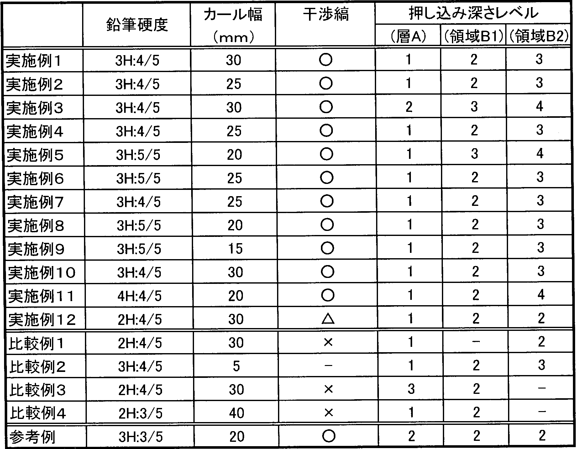
また、実施例及び参考例の光学積層体は、断面の電子顕微鏡観察において、ハードコート層(B)中に凹凸形状があるのが確認された。一方、比較例の光学積層体では、上記凹凸形状は確認できなかった。また、比較例2の光学積層体は、ハードコート層(B)用組成物中の無機微粒子の量が多く、無機微粒子含有領域(B2)のみになり、無機微粒子非含有領域(B1)が形成されなかった。
2 ハードコート層(A)
3 ハードコート層(B)
4 無機微粒子非含有領域(B1)
5 無機微粒子含有領域(B2)
Claims (11)
- 光透過性基材、前記光透過性基材の一方の面にハードコート層(A)及びハードコート層(B)をこの順に有する光学積層体であって、
前記ハードコート層(B)は、前記ハードコート層(A)と接している部分から順に、無機微粒子非含有領域(B1)と無機微粒子含有領域(B2)とを有し、
前記無機微粒子非含有領域(B1)と無機微粒子含有領域(B2)との境界は凹凸形状であり、
前記無機微粒子は、可視光波長よりも小さい粒径を有する
ことを特徴とする光学積層体。 - 無機微粒子非含有領域(B1)は、無機微粒子含有領域(B2)のバインダー樹脂を主成分とし、かつ、可視光波長以上の平均厚さを有する請求項1記載の光学積層体。
- ハードコート層(A)のバインダー樹脂と、ハードコート層(B)のバインダー樹脂とが相容性を有する請求項1又は2記載の光学積層体。
- ハードコート層(A)の硬度(Ha)と、無機微粒子非含有領域(B1)の硬度(Hb1)と、無機微粒子含有領域(B2)の硬度(Hb2)とが、下記式(1)を満たす請求項1、2又は3記載の光学積層体。
Ha≦Hb1<Hb2 (1) - 無機微粒子の形状が、数珠状である請求項1、2、3又は4記載の光学積層体。
- 無機微粒子は、導電性無機微粒子である請求項1、2、3、4又は5記載の光学積層体。
- 無機微粒子のハードコート層(B)中の含有量が10~80質量%である請求項1、2、3、4、5又は6記載の光学積層体。
- ハードコート層(B)のハードコート層(A)と反対側面に、低屈折率層を更に有する請求項1、2、3、4、5、6又は7記載の光学積層体。
- ハードコート層(B)のハードコート層(A)と反対側面に、防汚層を更に有する請求項1、2、3、4、5、6、7又は8記載の光学積層体。
- 偏光素子を有する偏光板であって、
前記偏光板は、前記偏光素子の表面に請求項1、2、3、4、5、6、7、8又は9記載の光学積層体を備えることを特徴とする偏光板。 - 最表面に請求項1、2、3、4、5、6、7、8若しくは9記載の光学積層体、又は、請求項10記載の偏光板を備えることを特徴とする画像表示装置。
Priority Applications (3)
| Application Number | Priority Date | Filing Date | Title |
|---|---|---|---|
| CN201080031279.XA CN102472842B (zh) | 2009-08-04 | 2010-07-02 | 光学层积体、偏振片和图像显示装置 |
| US13/388,886 US8795823B2 (en) | 2009-08-04 | 2010-07-02 | Optical layered body, polarizer and image display device |
| KR1020127003029A KR101452598B1 (ko) | 2009-08-04 | 2010-07-02 | 광학 적층체, 편광판 및 화상 표시 장치 |
Applications Claiming Priority (2)
| Application Number | Priority Date | Filing Date | Title |
|---|---|---|---|
| JP2009181938A JP5476843B2 (ja) | 2009-08-04 | 2009-08-04 | 光学積層体、偏光板及び画像表示装置 |
| JP2009-181938 | 2009-08-04 |
Publications (1)
| Publication Number | Publication Date |
|---|---|
| WO2011016306A1 true WO2011016306A1 (ja) | 2011-02-10 |
Family
ID=43544207
Family Applications (1)
| Application Number | Title | Priority Date | Filing Date |
|---|---|---|---|
| PCT/JP2010/061327 Ceased WO2011016306A1 (ja) | 2009-08-04 | 2010-07-02 | 光学積層体、偏光板及び画像表示装置 |
Country Status (6)
| Country | Link |
|---|---|
| US (1) | US8795823B2 (ja) |
| JP (1) | JP5476843B2 (ja) |
| KR (1) | KR101452598B1 (ja) |
| CN (1) | CN102472842B (ja) |
| TW (1) | TWI448718B (ja) |
| WO (1) | WO2011016306A1 (ja) |
Cited By (4)
| Publication number | Priority date | Publication date | Assignee | Title |
|---|---|---|---|---|
| WO2013015332A1 (ja) * | 2011-07-26 | 2013-01-31 | 大日本印刷株式会社 | 防眩性フィルム、偏光板及び画像表示装置 |
| WO2013099658A1 (ja) * | 2011-12-28 | 2013-07-04 | 大日本印刷株式会社 | 光学積層体及び画像表示装置 |
| US20140127463A1 (en) * | 2011-07-05 | 2014-05-08 | Mitsubishi Rayon Co., Ltd. | Article having micro uneven structure on surface thereof and video display device having the same |
| JPWO2013153648A1 (ja) * | 2012-04-12 | 2015-12-17 | フクビ化学工業株式会社 | 透明樹脂積層板 |
Families Citing this family (26)
| Publication number | Priority date | Publication date | Assignee | Title |
|---|---|---|---|---|
| JP5935393B2 (ja) * | 2011-03-03 | 2016-06-15 | 東レ株式会社 | 積層フィルム |
| JP6128576B2 (ja) * | 2011-04-22 | 2017-05-17 | 日東電工株式会社 | 光学積層体 |
| JP2012234164A (ja) * | 2011-04-22 | 2012-11-29 | Nitto Denko Corp | 光学積層体 |
| JP6128629B2 (ja) * | 2011-04-22 | 2017-05-17 | 日東電工株式会社 | 光学積層体 |
| JP5975032B2 (ja) | 2011-06-30 | 2016-08-23 | Jnc株式会社 | 耐候性積層フィルム |
| KR101501907B1 (ko) | 2011-11-07 | 2015-03-12 | 오지 홀딩스 가부시키가이샤 | 정전 용량식 터치 패널이 형성된 표시 장치, 정전 용량식 터치 패널 |
| JP6135134B2 (ja) * | 2012-06-04 | 2017-05-31 | 大日本印刷株式会社 | 光学積層体及び画像表示装置 |
| JPWO2013191154A1 (ja) * | 2012-06-18 | 2016-05-26 | イーエイチエス レンズ フィリピン インク | 光学物品及びコーティング液 |
| KR20130141995A (ko) * | 2012-06-18 | 2013-12-27 | 동우 화인켐 주식회사 | 하드코팅 필름, 이를 포함하는 편광판 및 화상 표시 장치 |
| US9087951B2 (en) * | 2012-09-28 | 2015-07-21 | Jinlin Ye | Method and apparatus for diffusion into semiconductor materials |
| JP6375946B2 (ja) * | 2013-01-09 | 2018-08-22 | 東レ株式会社 | 積層フィルム |
| KR20150024548A (ko) * | 2013-08-27 | 2015-03-09 | 동우 화인켐 주식회사 | 반사방지 광학 적층체 |
| JP6656799B2 (ja) | 2013-11-29 | 2020-03-04 | 王子ホールディングス株式会社 | アンチニュートンリング積層体およびそのアンチニュートンリング積層体を用いた静電容量式タッチパネル |
| US10365410B2 (en) * | 2014-03-14 | 2019-07-30 | Sharp Kabushiki Kaisha | Optical element and display device |
| JP6476694B2 (ja) * | 2014-09-29 | 2019-03-06 | 大日本印刷株式会社 | 転写シートの製造方法 |
| EP3141934B1 (en) | 2015-09-11 | 2020-10-07 | Canon Kabushiki Kaisha | Optical member comprising an antireflective film including a porous layer and method for manufacturing the same |
| US10359550B2 (en) * | 2016-08-31 | 2019-07-23 | Efx Energy Technologies, Llc | Multi-layered reflective insulation system |
| JP7118614B2 (ja) * | 2017-03-10 | 2022-08-16 | キヤノン株式会社 | 光学部材、撮像装置、及び光学部材の製造方法 |
| US10459123B2 (en) | 2017-03-10 | 2019-10-29 | Canon Kabushiki Kaisha | Optical member, image pickup apparatus, and method for manufacturing optical member |
| WO2018186262A1 (ja) * | 2017-04-06 | 2018-10-11 | 大日本印刷株式会社 | ポリイミドフィルム、積層体、及びディスプレイ用表面材 |
| JP7118615B2 (ja) * | 2017-10-12 | 2022-08-16 | キヤノン株式会社 | 光学素子、光学系および撮像装置 |
| JP7071813B2 (ja) * | 2017-10-16 | 2022-05-19 | 株式会社トッパンTomoegawaオプティカルフィルム | ハードコートフィルムの製造方法及び反射防止フィルムの製造方法 |
| JP6983302B2 (ja) * | 2018-02-13 | 2021-12-17 | 帝人株式会社 | 機能性微粒子を含有するハードコート層付基材の製造方法 |
| JP2020052352A (ja) * | 2018-09-28 | 2020-04-02 | ホヤ レンズ タイランド リミテッドHOYA Lens Thailand Ltd | 眼鏡レンズ |
| KR102363874B1 (ko) * | 2018-10-18 | 2022-02-15 | 주식회사 엘지화학 | 편광판, 액정 패널 및 디스플레이 장치 |
| TWI896551B (zh) * | 2019-09-24 | 2025-09-11 | 日商琳得科股份有限公司 | 觸控筆接觸片 |
Citations (5)
| Publication number | Priority date | Publication date | Assignee | Title |
|---|---|---|---|---|
| JPH08197670A (ja) * | 1995-01-27 | 1996-08-06 | Dainippon Printing Co Ltd | 表面保護シート及びその製造方法 |
| JP2002036436A (ja) * | 2000-07-19 | 2002-02-05 | Fuji Photo Film Co Ltd | ハードコートフイルム及び機能性薄膜付きハードコートフイルム |
| JP2007025077A (ja) * | 2005-07-13 | 2007-02-01 | Asahi Kasei Corp | 反射防止構造及びその製造方法並びに低屈折率層用塗布組成物 |
| JP2009114333A (ja) * | 2007-11-07 | 2009-05-28 | Konica Minolta Opto Inc | ハードコートフィルム、及びその製造方法 |
| JP2009134238A (ja) * | 2007-11-06 | 2009-06-18 | Konica Minolta Opto Inc | ハードコートフィルム、反射防止フィルム、偏光板及び表示装置 |
Family Cites Families (10)
| Publication number | Priority date | Publication date | Assignee | Title |
|---|---|---|---|---|
| JPH02160543A (ja) | 1989-11-16 | 1990-06-20 | Toray Ind Inc | 複層被膜 |
| JP3073270B2 (ja) | 1991-07-05 | 2000-08-07 | 触媒化成工業株式会社 | ハードコート膜付基材 |
| JP2000338308A (ja) * | 1999-05-31 | 2000-12-08 | Toray Ind Inc | 反射防止フィルム |
| JP4395349B2 (ja) * | 2003-09-29 | 2010-01-06 | 大日本印刷株式会社 | 光学フィルムおよびこの光学フィルムを具備する光学表示装置 |
| US9291745B2 (en) * | 2006-03-28 | 2016-03-22 | Dai Nippon Printing Co., Ltd. | Optical laminated body |
| WO2007114364A1 (ja) | 2006-03-31 | 2007-10-11 | Dai Nippon Printing Co., Ltd. | 光学積層体及び光学積層体の製造方法 |
| TWI416158B (zh) * | 2006-03-31 | 2013-11-21 | Dainippon Printing Co Ltd | Optical laminated body and optical laminate |
| US8163372B2 (en) | 2006-08-14 | 2012-04-24 | Dai Nippon Printing Co., Ltd. | Anti-dazzling optical laminate |
| US8597780B2 (en) * | 2007-08-10 | 2013-12-03 | Dai Nippon Printing Co., Ltd. | Hard coat film |
| JP5187621B2 (ja) | 2007-11-08 | 2013-04-24 | 株式会社リコー | クリーニング装置、並びにこれを用いたプロセスユニット及び画像形成装置 |
-
2009
- 2009-08-04 JP JP2009181938A patent/JP5476843B2/ja active Active
-
2010
- 2010-07-02 KR KR1020127003029A patent/KR101452598B1/ko active Active
- 2010-07-02 WO PCT/JP2010/061327 patent/WO2011016306A1/ja not_active Ceased
- 2010-07-02 US US13/388,886 patent/US8795823B2/en active Active
- 2010-07-02 CN CN201080031279.XA patent/CN102472842B/zh active Active
- 2010-07-09 TW TW99122595A patent/TWI448718B/zh active
Patent Citations (5)
| Publication number | Priority date | Publication date | Assignee | Title |
|---|---|---|---|---|
| JPH08197670A (ja) * | 1995-01-27 | 1996-08-06 | Dainippon Printing Co Ltd | 表面保護シート及びその製造方法 |
| JP2002036436A (ja) * | 2000-07-19 | 2002-02-05 | Fuji Photo Film Co Ltd | ハードコートフイルム及び機能性薄膜付きハードコートフイルム |
| JP2007025077A (ja) * | 2005-07-13 | 2007-02-01 | Asahi Kasei Corp | 反射防止構造及びその製造方法並びに低屈折率層用塗布組成物 |
| JP2009134238A (ja) * | 2007-11-06 | 2009-06-18 | Konica Minolta Opto Inc | ハードコートフィルム、反射防止フィルム、偏光板及び表示装置 |
| JP2009114333A (ja) * | 2007-11-07 | 2009-05-28 | Konica Minolta Opto Inc | ハードコートフィルム、及びその製造方法 |
Cited By (10)
| Publication number | Priority date | Publication date | Assignee | Title |
|---|---|---|---|---|
| US20140127463A1 (en) * | 2011-07-05 | 2014-05-08 | Mitsubishi Rayon Co., Ltd. | Article having micro uneven structure on surface thereof and video display device having the same |
| WO2013015332A1 (ja) * | 2011-07-26 | 2013-01-31 | 大日本印刷株式会社 | 防眩性フィルム、偏光板及び画像表示装置 |
| CN103620449A (zh) * | 2011-07-26 | 2014-03-05 | 大日本印刷株式会社 | 防眩性膜、偏振片和图像显示装置 |
| CN103620449B (zh) * | 2011-07-26 | 2015-12-23 | 大日本印刷株式会社 | 防眩性膜、偏振片和图像显示装置 |
| US10254444B2 (en) | 2011-07-26 | 2019-04-09 | Dai Nippon Printing Co., Ltd. | Anti-glare film, polarizer and image display device |
| WO2013099658A1 (ja) * | 2011-12-28 | 2013-07-04 | 大日本印刷株式会社 | 光学積層体及び画像表示装置 |
| CN104024892A (zh) * | 2011-12-28 | 2014-09-03 | 大日本印刷株式会社 | 光学层积体和图像显示装置 |
| JPWO2013099658A1 (ja) * | 2011-12-28 | 2015-05-07 | 大日本印刷株式会社 | 光学積層体及び画像表示装置 |
| US11169303B2 (en) | 2011-12-28 | 2021-11-09 | Dai Nippon Printing Co., Ltd. | Optical layered body and image display device |
| JPWO2013153648A1 (ja) * | 2012-04-12 | 2015-12-17 | フクビ化学工業株式会社 | 透明樹脂積層板 |
Also Published As
| Publication number | Publication date |
|---|---|
| CN102472842B (zh) | 2015-02-18 |
| TW201106005A (en) | 2011-02-16 |
| JP2011033948A (ja) | 2011-02-17 |
| US20120189828A1 (en) | 2012-07-26 |
| KR101452598B1 (ko) | 2014-10-21 |
| TWI448718B (zh) | 2014-08-11 |
| JP5476843B2 (ja) | 2014-04-23 |
| KR20120052277A (ko) | 2012-05-23 |
| US8795823B2 (en) | 2014-08-05 |
| CN102472842A (zh) | 2012-05-23 |
Similar Documents
| Publication | Publication Date | Title |
|---|---|---|
| JP5476843B2 (ja) | 光学積層体、偏光板及び画像表示装置 | |
| JP4116045B2 (ja) | 防眩性ハードコートフィルム | |
| KR100959049B1 (ko) | 방현성 하드 코트 필름 | |
| CN103080778B (zh) | 光学层叠体、偏振片和图像显示装置 | |
| JP5098662B2 (ja) | 光学積層体、偏光板及び画像表示装置 | |
| JP6070195B2 (ja) | 反射防止フィルム、反射防止フィルムの製造方法、偏光板及び画像表示装置 | |
| CN107718800B (zh) | 防眩性膜、偏振片和图像显示装置 | |
| CN103308959B (zh) | 光学膜、偏振片、液晶面板及图像显示装置 | |
| CN101410729B (zh) | 光学层积体 | |
| CN102640020B (zh) | 光学层积体及光学层积体的制造方法 | |
| CN101410247B (zh) | 光学层积体和光学层积体的制造方法 | |
| JP6268692B2 (ja) | 光学積層体、偏光板及び画像表示装置 | |
| WO2007142142A1 (ja) | 光学積層体、偏光板、及び、画像表示装置 | |
| JP2010085983A (ja) | 光学積層体、偏光板及び画像表示装置 | |
| JP2009098654A (ja) | 光学積層体、偏光板及び画像表示装置 | |
| JPWO2006106758A1 (ja) | 偏光板 | |
| JP2009075354A (ja) | 光学積層体、偏光板、及び、画像表示装置 | |
| JP2009258602A (ja) | 光学フィルム、偏光板、および画像表示装置 | |
| JP5051088B2 (ja) | 光学積層体、偏光板及び画像表示装置 | |
| JP6089547B2 (ja) | 光学積層体、偏光板及び画像表示装置 | |
| JP5096069B2 (ja) | 光学積層体、偏光板、及び、画像表示装置 | |
| JP5949755B2 (ja) | 光学積層体、偏光板及び画像表示装置 | |
| JP2012177700A (ja) | 光学積層体の防汚剤ブリードアウトの抑制状態の評価方法 |
Legal Events
| Date | Code | Title | Description |
|---|---|---|---|
| WWE | Wipo information: entry into national phase |
Ref document number: 201080031279.X Country of ref document: CN |
|
| 121 | Ep: the epo has been informed by wipo that ep was designated in this application |
Ref document number: 10806306 Country of ref document: EP Kind code of ref document: A1 |
|
| ENP | Entry into the national phase |
Ref document number: 20127003029 Country of ref document: KR Kind code of ref document: A |
|
| NENP | Non-entry into the national phase |
Ref country code: DE |
|
| WWE | Wipo information: entry into national phase |
Ref document number: 13388886 Country of ref document: US |
|
| 122 | Ep: pct application non-entry in european phase |
Ref document number: 10806306 Country of ref document: EP Kind code of ref document: A1 |