WO2010147201A1 - 電力変換装置 - Google Patents
電力変換装置 Download PDFInfo
- Publication number
- WO2010147201A1 WO2010147201A1 PCT/JP2010/060335 JP2010060335W WO2010147201A1 WO 2010147201 A1 WO2010147201 A1 WO 2010147201A1 JP 2010060335 W JP2010060335 W JP 2010060335W WO 2010147201 A1 WO2010147201 A1 WO 2010147201A1
- Authority
- WO
- WIPO (PCT)
- Prior art keywords
- electrode
- power conversion
- conductor
- terminal
- semiconductor element
- Prior art date
- Legal status (The legal status is an assumption and is not a legal conclusion. Google has not performed a legal analysis and makes no representation as to the accuracy of the status listed.)
- Ceased
Links
Images




















Classifications
-
- H—ELECTRICITY
- H10—SEMICONDUCTOR DEVICES; ELECTRIC SOLID-STATE DEVICES NOT OTHERWISE PROVIDED FOR
- H10W—GENERIC PACKAGES, INTERCONNECTIONS, CONNECTORS OR OTHER CONSTRUCTIONAL DETAILS OF DEVICES COVERED BY CLASS H10
- H10W70/00—Package substrates; Interposers; Redistribution layers [RDL]
- H10W70/40—Leadframes
- H10W70/479—Leadframes on or in insulating or insulated package substrates, interposers, or redistribution layers
-
- H—ELECTRICITY
- H10—SEMICONDUCTOR DEVICES; ELECTRIC SOLID-STATE DEVICES NOT OTHERWISE PROVIDED FOR
- H10W—GENERIC PACKAGES, INTERCONNECTIONS, CONNECTORS OR OTHER CONSTRUCTIONAL DETAILS OF DEVICES COVERED BY CLASS H10
- H10W44/00—Electrical arrangements for controlling or matching impedance
- H10W44/501—Inductive arrangements
-
- H—ELECTRICITY
- H10—SEMICONDUCTOR DEVICES; ELECTRIC SOLID-STATE DEVICES NOT OTHERWISE PROVIDED FOR
- H10W—GENERIC PACKAGES, INTERCONNECTIONS, CONNECTORS OR OTHER CONSTRUCTIONAL DETAILS OF DEVICES COVERED BY CLASS H10
- H10W72/00—Interconnections or connectors in packages
- H10W72/30—Die-attach connectors
-
- H—ELECTRICITY
- H10—SEMICONDUCTOR DEVICES; ELECTRIC SOLID-STATE DEVICES NOT OTHERWISE PROVIDED FOR
- H10W—GENERIC PACKAGES, INTERCONNECTIONS, CONNECTORS OR OTHER CONSTRUCTIONAL DETAILS OF DEVICES COVERED BY CLASS H10
- H10W74/00—Encapsulations, e.g. protective coatings
- H10W74/10—Encapsulations, e.g. protective coatings characterised by their shape or disposition
- H10W74/111—Encapsulations, e.g. protective coatings characterised by their shape or disposition the semiconductor body being completely enclosed
-
- H—ELECTRICITY
- H10—SEMICONDUCTOR DEVICES; ELECTRIC SOLID-STATE DEVICES NOT OTHERWISE PROVIDED FOR
- H10W—GENERIC PACKAGES, INTERCONNECTIONS, CONNECTORS OR OTHER CONSTRUCTIONAL DETAILS OF DEVICES COVERED BY CLASS H10
- H10W90/00—Package configurations
-
- H—ELECTRICITY
- H10—SEMICONDUCTOR DEVICES; ELECTRIC SOLID-STATE DEVICES NOT OTHERWISE PROVIDED FOR
- H10W—GENERIC PACKAGES, INTERCONNECTIONS, CONNECTORS OR OTHER CONSTRUCTIONAL DETAILS OF DEVICES COVERED BY CLASS H10
- H10W72/00—Interconnections or connectors in packages
- H10W72/071—Connecting or disconnecting
- H10W72/073—Connecting or disconnecting of die-attach connectors
- H10W72/07351—Connecting or disconnecting of die-attach connectors characterised by changes in properties of the die-attach connectors during connecting
- H10W72/07354—Connecting or disconnecting of die-attach connectors characterised by changes in properties of the die-attach connectors during connecting changes in dispositions
-
- H—ELECTRICITY
- H10—SEMICONDUCTOR DEVICES; ELECTRIC SOLID-STATE DEVICES NOT OTHERWISE PROVIDED FOR
- H10W—GENERIC PACKAGES, INTERCONNECTIONS, CONNECTORS OR OTHER CONSTRUCTIONAL DETAILS OF DEVICES COVERED BY CLASS H10
- H10W72/00—Interconnections or connectors in packages
- H10W72/30—Die-attach connectors
- H10W72/341—Dispositions of die-attach connectors, e.g. layouts
- H10W72/347—Dispositions of multiple die-attach connectors
-
- H—ELECTRICITY
- H10—SEMICONDUCTOR DEVICES; ELECTRIC SOLID-STATE DEVICES NOT OTHERWISE PROVIDED FOR
- H10W—GENERIC PACKAGES, INTERCONNECTIONS, CONNECTORS OR OTHER CONSTRUCTIONAL DETAILS OF DEVICES COVERED BY CLASS H10
- H10W72/00—Interconnections or connectors in packages
- H10W72/90—Bond pads, in general
- H10W72/921—Structures or relative sizes of bond pads
- H10W72/926—Multiple bond pads having different sizes
-
- H—ELECTRICITY
- H10—SEMICONDUCTOR DEVICES; ELECTRIC SOLID-STATE DEVICES NOT OTHERWISE PROVIDED FOR
- H10W—GENERIC PACKAGES, INTERCONNECTIONS, CONNECTORS OR OTHER CONSTRUCTIONAL DETAILS OF DEVICES COVERED BY CLASS H10
- H10W74/00—Encapsulations, e.g. protective coatings
Definitions
- the present invention relates to a power converter, and more particularly to a power converter including a semiconductor element for power conversion.
- a semiconductor is provided with an IGBT (semiconductor device for power conversion), a lead frame electrically connected to the IGBT, and a molding resin provided so as to include the IGBT and the lead frame in the inside.
- An apparatus power converter
- the lead frame is formed so as to protrude from the side surface of the molding resin so as to allow electrical connection with the outside.
- This invention was made in order to solve the above subjects, and one objective of this invention is to provide the power converter device which can attain size reduction.
- the power conversion device in the first aspect of the present invention is electrically connected to a power conversion semiconductor element having an electrode and an electrode of the power conversion semiconductor element, and is substantially flat with a side surface A conductor for an electrode including an upper end portion having an upper end face, and a sealing material made of a resin that covers the power conversion semiconductor element and a side surface of the conductor for an electrode.
- the sealing material exposes the substantially flat upper end surface of the electrode conductor on the upper surface of the sealing material, and protrudes laterally to the upper end portion having the substantially flat upper end surface of the exposed electrode conductor A protrusion is provided.
- the upper end surface of the conductor for electrodes of this invention means the end surface on the upper side relatively with respect to the lower surface connected to the semiconductor element.
- the substantially flat upper end surface of the electrode conductor is exposed on the upper surface of the sealing material, and the substantially flat upper surface of the exposed electrode conductor A laterally projecting projection is provided at the upper end having an end face.
- the heat generated from the power conversion semiconductor element can be dissipated upward through the electrode conductor.
- the area of the upper end surface (that is, the heat dissipation surface) of the conductor for electrode can be increased by the projecting portion that protrudes laterally. As a result, the amount of heat released when the heat generated from the power conversion semiconductor element is released upward can be increased.
- the electrode is made of the sealing material in order to connect the power conversion device and the external wiring. Unlike when protruding from the side, the power converter can be suppressed from becoming large. As a result, the power converter can be miniaturized.
- FIG. 2 is a cross-sectional view taken along line 1000-1000 of FIG.
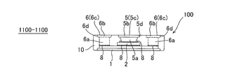
- FIG. 2 is a cross-sectional view taken along the line 1100-1100 in FIG.
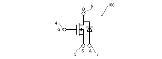
- FIG. 1 is a circuit diagram of a power module according to a first embodiment of the present invention.
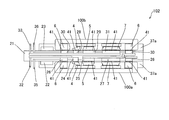
- FIG. 5 is a cross-sectional view of a power module according to a second embodiment of the present invention.
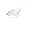
- FIG. 7 is a cross-sectional view of a power module according to a third embodiment of the present invention. It is the perspective view seen from the surface side of the power module by 4th Embodiment of this invention. It is a top view of the power module by a 5th embodiment of the present invention.
- FIG. 1 is a circuit diagram of a power module according to a first embodiment of the present invention.
- FIG. 5 is a cross-sectional view of a power module according to a second embodiment of the present invention.
- FIG. 7 is a cross-sectional view of a power module according to a third embodiment of the present invention. It is the perspective view seen from the surface side of the power module by 4th Embodiment of this invention. It is a top view of the power module by a 5th embodiment of
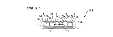
- FIG. 15 is a cross-sectional view taken along the line 1210-1210 of FIG.
- FIG. 15 is a cross-sectional view taken along line 1220-1220 in FIG. It is the perspective view seen from the surface side of the power module by 5th Embodiment of this invention. It is the perspective view seen from the back surface side of the power module by 5th Embodiment of this invention.
- FIG. 21 is a plan view of a power module according to a sixth embodiment of the present invention.
- FIG. 21 is a cross-sectional view taken along line 1230-1230 in FIG.
- FIG. 21 is a cross-sectional view taken along line 1240-1240 in FIG. It is the perspective view seen from the surface side of the power module by 6th Embodiment of this invention.
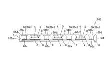
- FIG. 21 is a cross-sectional view of a power module according to a seventh embodiment of the present invention. It is the perspective view seen from the surface side of the power module by 7th Embodiment of this invention. It is the perspective view seen from the back surface side of the power module by 7th Embodiment of this invention.
- FIG. 18 is a cross-sectional view of a power module according to an eighth embodiment of the present invention. It is the perspective view seen from the surface side of the power module by 8th Embodiment of this invention. It is the perspective view seen from the back surface side of the power module by 8th Embodiment of this invention.
- FIG. 21 is a cross-sectional view of a power module according to a seventh embodiment of the present invention. It is the perspective view seen from the surface side of the power module by 7th Embodiment of this invention. It is the perspective view seen from the back surface side of the power module by 7th Embodiment of this invention.
- FIG. 18 is a cross-sectional view of a power
- FIG. 21 is a cross-sectional view of a power module according to a ninth embodiment of the present invention.
- FIG. 21 is a perspective view of a power module according to a ninth embodiment of the present invention.
- FIG. 21 is a plan view of a power module according to a tenth embodiment of the present invention.
- FIG. 33 is a cross-sectional view taken along line 1250-1250 in FIG. 32.
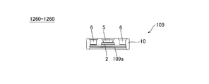
- FIG. 33 is a cross-sectional view of FIG. 32 taken along line 1260-1260.
- FIG. 21 is a plan view of a power module according to an eleventh embodiment of the present invention.
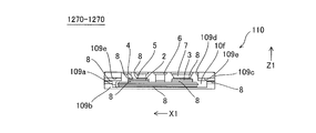
- FIG. 36 is a cross-sectional view taken along line 1270-1270 in FIG.
- FIG. 36 is a cross-sectional view taken along the line 1280-1280 in FIG. It is the perspective view seen from the surface side of the power module by 11th Embodiment of this invention. It is the perspective view seen from the back surface side of the power module by 11th Embodiment of this invention
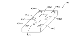
- a power module 100 according to a first embodiment of the present invention will be described with reference to FIGS. 1 to 10.
- the power module 100 is an example of the “power conversion device main unit” in the present invention.
- the drain electrode heat sink 1, the semiconductor element 2, the semiconductor element 3, the gate terminal 4 and the source terminal 5 , A drain terminal 6 and an anode terminal 7 are provided.
- the drain electrode heat sink 1, the gate terminal 4, the source terminal 5, the drain terminal 6, and the anode terminal 7 are made of metal such as copper (Cu) or copper molybdenum (CuMo).
- the drain electrode heat sink 1 consists only of the metal plate of 1 sheet which does not contain an insulator.
- the semiconductor element 2 is formed on a SiC substrate containing silicon carbide (SiC) as a main component, and is formed of a high frequency switchable FET (field effect transistor).
- the semiconductor element 2 has a control electrode 2 a and a source electrode 2 b provided on the main surface of the semiconductor element 2, and a drain electrode 2 c provided on the back surface.
- the semiconductor element 2 is an example of the “power conversion semiconductor element” or the “voltage drive type transistor element” in the present invention.
- the control electrode 2a is an example of the "surface electrode” in the present invention.
- the source electrode 2 b is an example of the “first electrode” and the “surface electrode” in the present invention.
- the drain electrode 2c is an example of the "second electrode” and the "back electrode” in the present invention.
- the drain electrode heat sink 1 is an example of the "heat radiating member" of this invention.
- the semiconductor element 3 is also formed of a fast recovery diode (FRD) having an anode electrode 3a and a cathode electrode 3b.
- the cathode electrode 3b of the semiconductor element 3 is electrically connected to the drain electrode 2c of the semiconductor element 2, and the semiconductor element 3 has a function as a reflux diode (see FIG. 10).
- the anode electrode 3a is an example of the "first diode electrode” in the present invention.
- the cathode electrode 3b is an example of the "second diode electrode” in the present invention.
- the semiconductor device 3 is an example of the “semiconductor device for power conversion” and the “reflux diode device” in the present invention.
- the anode electrode 3a and the cathode electrode 3b are examples of the "first diode electrode” and the "second diode electrode” in the present invention respectively.
- the semiconductor element 2 and the semiconductor element 3 are respectively bonded on the surface of the drain electrode heat sink 1 via the bonding material 8.
- the drain electrode 2 c of the semiconductor element 2 is electrically connected to the drain electrode heat dissipation plate 1
- the cathode electrode 3 b of the semiconductor element 3 is electrically connected to the drain electrode heat dissipation plate 1.
- the bonding material 8 is formed of solder having high heat resistance such as Au-20Sn, Zn-30Sn, Pb-5Sn or the like.
- the bonding material 8 is formed of organic layer-coated nano Ag particles or the like having higher heat resistance.
- the gate terminal 4 is bonded on the surface of the semiconductor element 2 (on the control electrode 2 a) via the bonding material 8. Further, as shown in FIG. 4, in the first embodiment, the gate terminal 4 has a columnar portion 4 a having a columnar shape and an upper end portion 4 b.
- the pillar-shaped portion 4a of the gate terminal 4 is formed to extend from above the surface of the semiconductor element 2 toward the upper side (arrow Z1 direction) of the power module 100 and to extend to the outer side (arrow X1 direction) of the power module 100 It is done.
- the upper end 4b of the gate terminal 4 has a substantially flat upper end face 4c.
- the upper end portion 4b is provided with a protruding portion 4d which protrudes in the side direction (direction orthogonal to the arrow Z1 direction).
- the protrusion 4 d is formed to circumferentially protrude from the outer peripheral surface of the columnar portion 4 a of the gate terminal 4.
- the upper end surface 4c of the gate terminal 4 is substantially flat and has a substantially rectangular shape (see FIG. 1) larger than the outer peripheral surface of the pillar shaped portion 4a (gate terminal 4) in plan view.
- the gate terminal 4 has a function of radiating heat generated by the semiconductor element 2 from the upper end surface 4c of the upper end portion 4b provided with the projecting portion 4d.
- the gate terminal 4 is an example of the “electrode conductor”, the “first electrode conductor”, the “first transistor electrode conductor”, and the “control electrode conductor” in the present invention.
- the source terminal 5 is bonded on the surface of the semiconductor element 2 (on the source electrode 2 b) via the bonding material 8. Further, as shown in FIG. 5, in the first embodiment, the source terminal 5 has a columnar portion 5 a having a columnar shape and an upper end portion 5 b. The columnar portion 5 a of the source terminal 5 is formed to extend from above the surface of the semiconductor element 2 toward the upper side (the direction of the arrow Z 1) of the power module 100. Further, the upper end portion 5b of the source terminal 5 has a substantially flat upper end surface 5c, and the upper end portion 5b is provided with a projecting portion 5d projecting laterally.
- the protruding portion 5 d is formed so as to circumferentially protrude from the outer peripheral surface of the columnar portion 5 a of the source terminal 5.
- the upper end surface 5c of the source terminal 5 is substantially flat and has a substantially rectangular shape (see FIG. 1) larger than the outer peripheral surface of the columnar portion 5a (the source terminal 5) in plan view.
- the source terminal 5 has a function of radiating heat generated by the semiconductor element 2 from the upper end surface 5c of the upper end portion 5b provided with the protrusion 5d.
- the source terminal 5 is an example of the “electrode conductor”, the “first electrode conductor”, the “first transistor electrode conductor”, and the “source electrode conductor” in the present invention.
- a recess 5 e is provided at the root of the column-shaped portion 5 a of the source terminal 5. That is, the source terminal 5 is formed such that the cross-sectional area increases from the base portion in which the recess 5 e is formed to the upper end 5 b in which the protrusion 5 d is provided. Thereby, it is possible to easily diffuse the heat propagating from the source electrode 2b of the semiconductor element 2 toward the upper end 5b.
- the surplus bonding material 8 can be disposed in the region where the recess 5e is formed by using the surface tension of the bonding material 8, so the surplus bonding material It is possible to suppress the occurrence of a short circuit or the like when 8 protrudes from the source electrode 2b.
- the drain terminal 6 is bonded on the surface of the drain electrode heat sink 1 via the bonding material 8. Further, as shown in FIG. 1, six drain terminals 6 are formed in the outer peripheral portion on the surface of the drain electrode heat sink 1 so as to surround the semiconductor element 2 and the semiconductor element 3. Specifically, one drain terminal 6 is provided at each of the four corners of the drain electrode heat sink 1, and one is provided near the central portion on the long side of the drain electrode heat sink 1. Thus, in the first embodiment, the drain terminal 6 is disposed at a position separated from the semiconductor element 2 and the semiconductor element 3 and disposed near the end of the power module 100 (see FIG. 1).
- the drain terminal 6 has a columnar portion 6a having a columnar shape and an upper end portion 6b.
- the columnar portion 6 a of the drain terminal 6 is formed to extend from above the surface of the drain electrode heat sink 1 toward the upper side (the direction of the arrow Z 1) of the power module 100.
- the upper end portion 6b of the drain terminal 6 has a substantially flat upper end surface 6c, and the upper end portion 6b is provided with a projecting portion 6d which protrudes laterally.
- the protrusion 6 d is formed so as to circumferentially protrude laterally from the outer peripheral surface of the columnar portion 6 a of the drain terminal 6.
- the upper end face 6c of the drain terminal 6 is substantially flat and has a substantially rectangular shape (see FIG. 1) larger than the outer peripheral surface of the columnar portion 6a (drain terminal 6) in plan view.
- the drain terminal 6 has a function of radiating heat generated by the semiconductor element 2 from the upper end surface 6c of the upper end portion 6b provided with the protrusion 6d.
- the height from the surface of the drain electrode heat sink 1 of the upper end surface 6c of the six drain terminals 6 is substantially the same, respectively.
- the drain terminal 6 is an example of the “electrode conductor”, the “second electrode conductor”, the “second transistor electrode conductor”, and the “drain electrode conductor” in the present invention.
- the drain terminal 6 is electrically connected to the cathode electrode 3 b of the semiconductor element 3 and also functions as a cathode electrode terminal of the semiconductor element 3. That is, the drain terminal 6 is also an example of the “second diode electrode conductor” in the present invention.
- the anode terminal 7 is disposed and fixed on the surface of the semiconductor element 3 (on the anode electrode 3 a) via the bonding material 8. Further, as shown in FIG. 7, in the first embodiment, the anode terminal 7 has a column-shaped portion 7 a having a column shape and an upper end portion 7 b. The columnar portion 7 a of the anode terminal 7 is formed to extend from above the surface of the semiconductor element 3 toward the upper side (the direction of the arrow Z 1) of the power module 100. Further, the upper end portion 7b of the anode terminal 7 has a substantially flat upper end surface 7c, and the upper end portion 7b is provided with a projecting portion 7d which protrudes laterally.
- the protrusion 7 d is formed to protrude circumferentially from the outer peripheral surface of the column-shaped portion 7 a.
- the upper end surface 7c of the anode terminal 7 is substantially flat and has a substantially rectangular shape (see FIG. 1) larger than the outer peripheral surface of the columnar portion 7a (anode terminal 7) in plan view.
- the anode terminal 7 has a function of radiating the heat generated by the semiconductor element 3 from the upper end surface 7 c of the upper end 7 b provided with the protrusion 7 d.
- the anode terminal 7 is an example of the “electrode conductor”, the “first electrode conductor”, and the “first diode electrode conductor” in the present invention.
- a recess 7 e is provided at the root of the column-shaped portion 7 a of the anode terminal 7.
- the surplus bonding material 8 can be disposed in the region where the recess 7e is formed by utilizing the surface tension of the bonding material 8, the surplus bonding material It is possible to suppress the occurrence of a short circuit or the like when 8 protrudes from the anode electrode 3a.
- the upper end face 5c, the upper end face 6c of the upper end 6b where the protrusion 6d of the drain terminal 6 is provided, and the upper end face 7c of the upper end 7b where the protrusion 7d of the anode terminal 7 is provided have substantially the same height. It is formed as.
- each terminal is a column-shaped portion (column-shaped portion 4a, column-shaped portion 5a, column-shaped portion 6a, and column). It may be formed integrally with the shape portion 7a), or may be formed separately from the column shape portion (a column shape portion 4a, a column shape portion 5a, a column shape portion 6a, and a column shape portion It may be joined to the upper surface of 7a).
- bonding between the semiconductor element and the electrode is performed by wiring such as wire bonding.
- wiring such as wire bonding since the wiring inductance becomes relatively large, it is difficult to switch the power module at high frequency.
- the gate terminal 4, the source terminal 5 and the drain terminal 6 (anode terminal 7) of the first embodiment are each directly bonded to the semiconductor element 2 (semiconductor element 3) through the bonding material 8. Since the wiring inductance is reduced compared to the case of using bonding, it is possible to switch the power module 100 at high frequency.
- the side surfaces of the semiconductor element 2, the semiconductor element 3, the gate terminal 4, the source terminal 5, the drain terminal 6, the anode terminal 7 and the drain electrode heat sink 1 An insulating resin material 10 made of silicon gel or the like is provided to cover it so as to surround it.
- the resin material 10 forms the outer surface of the power module 100.
- the resin material 10 has a function as an insulator performing insulation between the semiconductor element 2, the semiconductor element 3, the gate terminal 4, the source terminal 5, the drain terminal 6 and the anode terminal 7, and the semiconductor element 2 and the semiconductor element 3. It has a function as a sealing material which prevents the penetration of moisture and the like.
- the resin material 10 is an example of the “sealing material” in the present invention.
- the resin material 10 has the upper end surface 4 c of the gate terminal 4, the upper end surface 5 c of the source terminal 5, the upper end surface 6 c of the drain terminal 6, and the upper end surface of the anode terminal 7. 7c are provided to be exposed from the top surface.
- the upper surface of the resin material 10 has substantially the same height as the upper end surface 4 c of the gate terminal 4, the upper end surface 5 c of the source terminal 5, the upper end surface 6 c of the drain terminal 6 and the upper end surface 7 c of the anode terminal 7.
- the upper end surface 4c of the gate terminal 4 exposed from the resin material 10, the upper end surface 5c of the source terminal 5, the upper end surface 6c of the drain terminal 6, and the upper end surface 7c of the anode terminal 7 are electrically connected to the outside. It is configured to be Further, as shown in FIG. 9, the drain electrode heat sink 1 is exposed from the back surface of the resin material 10.
- the semiconductor element 2 and the semiconductor element are obtained from both the upper end face 6c of the drain terminal 6 and the upper end face 7c of the anode terminal 7 and the drain electrode heat sink 1 disposed on the lower surface (rear surface) side of the semiconductor element 2 and the semiconductor element 3 It is comprised so that the heat which generate
- the upper end surface 7c) is exposed.
- the upper end portion 6b and the upper end portion 7b) are provided with protruding portions 4d (protruding portions 5d, 6d and 7d) protruding sideways.
- the heat generated from the semiconductor element 2 and the semiconductor element 3 can be radiated upward through the gate terminal 4 (the source terminal 5, the drain terminal 6, the anode terminal 7).
- the upper end surface 4c (upper end surface 5c, upper portion) of the gate terminal 4 (the source terminal 5, the drain terminal 6, and the anode terminal 7) is formed by the protruding portion 4d (protruding portion 5d, protruding portion 6d, and protruding portion 7d) Since the area of the end face 6c and the upper end face 7c, that is, the heat dissipation surface can be increased, the amount of heat dissipation can be increased when heat generated from the semiconductor element 2 and the semiconductor element 3 is dissipated upward.
- the upper end 4b (upper end 5b, upper end 6b, upper end) of the gate terminal 4 (source terminal 5, drain terminal 6, anode terminal 7) having a pillar shape extending upward
- the protrusion 4d (the protrusion 5d, the protrusion 6d, the protrusion 7d) of the portion 7b is circumferentially protruded from the outer peripheral surface of the column-shaped gate terminal 4 (the source terminal 5, the drain terminal 6, the anode terminal 7). To set up.
- the area of the upper end surface 4c (upper end surface 5c, upper end surface 6c, upper end surface 7c) (i.e., heat dissipation surface) of the gate terminal 4 (source terminal 5, drain terminal 6, anode terminal 7) is easily increased. be able to.
- the gate terminal 4 (the source terminal 5, the drain terminal 6, and the anode terminal 7) provided with the projection 4d (the projection 5d, the projection 6d, and the projection 7d) as described above.
- the substantially flat upper end face 4c (upper end face 5c, upper end face 6c, and upper end face 7c) is configured to have substantially the same height.
- the gate terminal 4 (the source terminal 5, the drain terminal 6, and the anode terminal 7) provided with the projection 4d (the projection 5d, the projection 6d, and the projection 7d) as described above.
- the substantially flat upper end face 4c (upper end face 5c, upper end face 6c, upper end face 7c) is configured to have substantially the same height as the upper face of the resin material 10.
- the upper end surface 4c, the upper end surface 5c, the upper end surface 6c and the upper end surface 7c are flush with the upper surface of the resin material 10. Therefore, the upper end surface 4c, the upper end surface 5c, the upper end surface 6c and the upper end surface 7c A wiring board or the like can be easily disposed on the resin material 10.
- electrical connection with the outside is performed in each of the upper end surfaces 7c.
- heat is dissipated at each of the upper end surface 4 c of the gate terminal 4, the upper end surface 5 c of the source terminal 5, the upper end surface 6 c of the drain terminal 6 and the upper end surface 7 c of the anode terminal 7 exposed to the upper surface of the resin material 10. Both electrical connection with the outside can be made simultaneously.
- the gate terminal 4 (the source terminal 5) is connected to the control electrode 2a (the source electrode 2b) on the main surface of the semiconductor element 2 via the bonding material 8
- a substantially flat upper end surface 4c (upper end surface 5c) exposed from the upper surface of the resin material 10 and a protrusion 4d (a protrusion 5d) are provided while extending upward.
- the drain terminal 6 extends upward from a position separated from the semiconductor element 2 in a state of being electrically connected to the drain electrode 2 c on the back surface of the semiconductor element 2 and is substantially flat exposed from the upper surface of the resin material 10. It has an upper end face 6c and a protrusion 6d.
- the anode terminal 7 extends upward in a state of being connected to the anode electrode 3 a via the bonding material 8 on the main surface of the semiconductor element 3, and a substantially flat upper end surface 7 c exposed from the upper surface of the resin material 10. And a protrusion 7d.
- the drain terminal 6 extends upward from a position separated from the semiconductor element 3 in a state of being electrically connected to the cathode electrode 3 b on the back surface of the semiconductor element 3, and is substantially flat exposed from the upper surface of the resin material 10. It has an upper end face 6c and a protrusion 6d.
- the upper end surface 4c of the gate terminal 4, the upper end surface 5c of the source terminal 5, the upper end surface 6c of the drain terminal 6, and the upper end surface 7c of the anode terminal 7 are disposed above the power module 100. Can be easily connected.
- the areas of the upper end surface 4c of the gate terminal 4 functioning as a heat dissipation surface, the upper end surface 5c of the source terminal 5, the upper end surface 6c of the drain terminal 6 and the upper end surface 7c of the anode terminal 7 are respectively protruding portions 4d (protruding portions 5d, Since the size can be increased by the protrusion 6 d and the protrusion 7 d), the amount of heat released when the heat generated from the semiconductor element 2 and the semiconductor element 3 is released upward can be further increased.
- the end face 6c is formed to be exposed.
- both the substantially flat upper end surface 4c of the gate terminal 4 of the semiconductor element 2 and the substantially flat upper end surface 5c of the source terminal 5 and the substantially flat upper end surface 6c of the drain terminal 6 are on the upper side of the power module 100.
- the projection 4d (the projection 5d and the projection 6d) is large in size, so that electrical connection with the outside can be easily performed.
- the drain terminal 6 extends upward from a position separated from the semiconductor element 2 in a state of being electrically connected to the drain electrode 2 c on the back surface of the semiconductor element 2. Configure. Then, the drain terminal 6 is provided with a substantially flat upper end face 6 c and a protrusion 6 d. As a result, since the drain terminal 6 and the semiconductor element 2 are separated, a short circuit between the side surface of the drain terminal 6 and the semiconductor element 2 can be suppressed.
- the gate terminal 4 and the source terminal 5 can be arranged in the central portion of the power module 100 by arranging the drain terminal 6 in the vicinity of the end of the power module 100. it can. As a result, the distance between the drain terminal 6 and the gate terminal 4 and the source terminal 5 can be increased, so that a short circuit between the drain terminal 6 and the gate terminal 4 and the source terminal 5 can be suppressed.
- the resin material 10 covers the semiconductor element 3 and the side surface of the anode terminal 7, and the upper surface 7 c of the anode terminal 7 is substantially flat on the upper surface of the resin material 10.
- the heat generated from the semiconductor element 3 can be radiated upward from the substantially flat upper end surface 7c of the anode terminal 7.
- the area of the upper end surface 7c (heat radiating surface) of the anode terminal 7 can be enlarged by the protrusion part 7d which protrudes sideward.
- the amount of heat released when the heat generated from the semiconductor element 3 is released upward can be increased.
- the semiconductor element 2, the semiconductor element 3, the gate terminal 4, the source terminal 5, and the drain terminal 6 are provided by providing the resin material 10 so as to constitute the outer surface of the power module 100. Since the anode terminal 7 and the anode terminal 7 are included inside the resin material 10, damage to the semiconductor elements 2 and 3 due to an external impact can be suppressed. In addition, short circuit between the gate terminal 4, the source terminal 5, the drain terminal 6 and the anode terminal 7 can be suppressed.
- the semiconductor element 2 and the semiconductor element 3 are generated from both the upper end surface 6c and the upper end surface 7c of the anode terminal 7 and the drain electrode heat sink 1 disposed on the lower surface (rear surface) side of the semiconductor element 2 and the semiconductor element 3 To be able to dissipate heat.
- the heat can be radiated upward from the upper end surface 4c of the gate terminal 4 exposed from the upper surface of the resin material 10, the upper end surface 5c of the source terminal 5, the upper end surface 6c of the drain terminal 6 and the upper end surface 7c of the anode terminal 7 . Furthermore, since the heat can be dissipated downward from the drain electrode heat sink 1 disposed on the back surface side of the semiconductor element 2 and the semiconductor element 3, the amount of heat dissipation can be further increased.
- the drain electrode heat sink 1 is joined to the back surfaces of the semiconductor element 2 and the semiconductor element 3 via the bonding material 8, respectively. It can be easily bonded to the back surfaces of the semiconductor device 2 and the semiconductor device 3 respectively.
- the drain electrode heat sink 1 by forming the drain electrode heat sink 1 with a metal plate not containing an insulator, the drain electrode heat sink 1 differs from the case where the insulator 1 is contained, The amount of heat released from the electrode heat sink 1 can be increased.
- the resin material 10 is disposed so as to surround the drain electrode heat sink 1 and expose the surface of the drain electrode heat sink 1, thereby the surface of the drain electrode heat sink 1
- the amount of heat released from the drain electrode heat sink 1 can be increased.
- the semiconductor element 2 when the semiconductor element 2 (semiconductor element 3) is formed of a semiconductor made of SiC, the semiconductor element 2 (semiconductor element 3) is formed of a semiconductor made of Si.
- the semiconductor element 2 (semiconductor element 3) can be operated at high temperature and at high speed.
- the power modules 100 (power module main body portions 100 a and 100 b) of the first embodiment are attached to the wiring board 21.
- the power module main parts 100a and 100b are examples of the "power conversion device main part" in the present invention.
- the power module body parts 100a and 100b are attached to the wiring substrate 21 made of glass epoxy, ceramic, polyimide or the like. Further, on the lower surface of the wiring substrate 21, a P-side gate driver IC 22 and an N-side gate driver IC 23 are mounted.
- the power module 101 constitutes a three-phase inverter circuit.
- the power module body 100a functions as an upper arm of the three-phase inverter circuit
- the power module body 100b functions as a lower arm of the three-phase inverter circuit.
- the power module body 100 a is attached to the wiring board 21 via the bump electrode 41. That is, in the second embodiment, substantially flat upper end face 4c (upper end face 5c, upper end face 6c, upper end face) of gate terminal 4 (source terminal 5, drain terminal 6, anode terminal 7) exposed from the surface of resin material 10 7c) (see FIG. 1) electrically connect the P-side gate metal terminal 24 (P-side source metal terminal 25, P-side drain metal terminal 26, P-side anode metal terminal 27) of the wiring substrate 21 through the bump electrode 41 respectively. Connected. Further, the power module body 100 b is attached to the wiring board 21 via the bump electrode 41.
- substantially flat upper end face 4c (upper end face 5c, upper end face 6c, upper end face) of gate terminal 4 (source terminal 5, drain terminal 6, anode terminal 7) exposed from the surface of resin material 10 7c) (see FIG. 1) electrically connect the N-side gate metal terminal 28 (N-side source metal terminal 29, N-side drain metal terminal 30, N-side anode metal terminal 31) of the wiring board 21 via the bump electrode 41 It is connected to the.
- a P-side metal terminal 32 and an N-side metal terminal 33 are provided on one end side of the wiring board 21.
- the P-side metal terminal 32 is connected to the P-side drain metal terminal 26 of the power module main body 100 a through a bus bar-shaped wire 34 made of a conductive metal plate provided inside the wiring board 21.
- the P-side source metal terminal 25 and the P-side anode metal terminal 27 of the power module body 100a are connected to the N-side drain of the power module body 100b via the bus bar-like wiring 34 provided inside the wiring board 21. It is connected to the metal terminal 30.
- the N-side source metal terminal 29 and the N-side anode metal terminal 31 of the power module body 100 b are N-side metal provided on one end side of the wiring board 21 via the wiring 34 provided inside the wiring board 21. It is connected to the terminal 33.
- the P-side gate driver IC 22 is disposed in the vicinity of the power module main body 100a. Further, the P-side gate driver IC 22 is connected to a P-side control signal terminal 35 provided on one end side of the wiring board 21.
- the N-side gate driver IC 23 is disposed in the vicinity of the power module main body 100b. Further, the N-side gate driver IC 23 is connected to an N-side control signal terminal 36 provided on one end side of the wiring board 21.
- the wiring inductance can be reduced by arranging the P-side gate driver IC 22 and the N-side gate driver IC 23 in the vicinity of the power module body 100a and the power module body 100b, respectively, the power module body can be reduced. It is possible to switch 100a and the power module body 100b at high frequency.
- the wiring board 21, the power module main body 100a and the power module main body 100b are arranged slightly apart from each other, and between the wiring board 21 and the power module main body 100a and the power module main body 100b.
- An insulating resin material 37 is provided in the space (space).
- the wiring board 21 is fixed to the power module body 100a and the power module body 100b, and the bump electrode connecting the wiring board 21 to the power module body 100a and the power module body 100b. It is possible to suppress the corrosion of 41.
- the material of the resin material 37 is selected appropriately in accordance with the heat generation temperature of the semiconductor element 2 and the semiconductor element 3 and the like.
- the resin material 37 is an example of the “sealing material” in the present invention.
- the substantially flat upper end surface 4c (upper end surface 5c, 5c) of the gate terminal 4 (the source terminal 5, the drain terminal 6, and the anode terminal 7) exposed from the upper surface of the resin material 10.
- the upper end face 5 c and the upper end face 7 c are electrically connected by the wiring board 21 and the bump electrode 41.
- the distance between the substantially flat upper end surface 4c (upper end surface 5c, upper end surface 5c, upper end surface 7c) of the gate terminal 4 (source terminal 5, drain terminal 6, anode terminal 7) and the wiring substrate 21 is reduced. Therefore, corrosion of the gate terminal 4 (the source terminal 5, the drain terminal 6, the anode terminal 7) and the wiring board 21 can be suppressed.
- the power module body 100 b and the power module body 100 a are respectively disposed on the upper surface and the lower surface of the wiring board 21.
- the wiring for connecting the power module body 100a and the power module body 100b is used. Since the length is reduced, the wiring inductance can be reduced. As a result, the power module body 100a and the power module body 100b can be switched at high frequency.
- an insulating resin material 37a is provided to seal between the power module main body portions 100a and 100b and the wiring board 21.
- the resin material 37a is provided so as to cover the surface of the wiring board 21 and the central portions of the side surfaces of the power module main portions 100a and 100b.
- power module body portions 100a and 100b and wiring board 21 P side gate metal terminal 24, P side source metal terminal 25, P side drain metal terminal 26, P side anode metal terminal 27, N side gate metal terminal 28, N
- the distance between the power module main portions 100a and 100b and the wiring substrate 21 is reduced. .
- the resin material 37 a is an example of the “sealing material” in the present invention.
- the semiconductor element 2 and the semiconductor element 3 are provided in pairs (two).
- semiconductor elements 2 (see FIG. 1) and semiconductor elements 3 (see FIG. 1) are provided so as to be arranged in pairs (two). . That is, on the upper surface of the power module 103, the upper end surface 54a and the upper end surface 54b of each of the gate terminals 4 of the two semiconductor elements 2 and the upper end surface 55a and the upper end surface 55b of each of the source terminals 5 Exposed from Further, on the upper surface of the power module 102, the upper end surface 57a and the upper end surface 57b of the anode terminals 7 of the two semiconductor elements 3 are exposed from the resin material 10a.
- the resin material 10 a is an example of the “sealing material” in the present invention.
- the power module 103 is an example of the “power conversion device main unit” in the present invention.
- the semiconductor element 2 is provided without the semiconductor element 3 being provided.
- the shapes of the gate terminal 4 (see FIG. 4), the source terminal 5 (see FIG. 5), and the drain terminal 6 (see FIG. 6) are the same as those in the first embodiment. That is, the upper end 4b of the gate terminal 4, the upper end 5b of the source terminal 5, and the upper end 6b of the drain terminal 6 are respectively provided with a protrusion 4d, a protrusion 5d and a protrusion 6d protruding laterally. It is done. Further, as shown in FIG.
- the upper end surface 4 c of the gate terminal 4, the upper end surface 5 c of the source terminal 5, and the upper end surface 6 c of the drain terminal 6 are exposed from the resin material 10 b on the upper surface of the power module 104.
- the drain electrode heat sink 1 is exposed from the resin material 10 b on the lower surface of the power module 104.
- the resin material 10 b is an example of the “sealing material” in the present invention.
- the power module 104 is an example of the “power conversion device main unit” in the present invention.
- the semiconductor element 3 is provided without the semiconductor element 2 being provided.
- the shapes of the anode terminal 7 (see FIG. 7) and the drain terminal 6 (see FIG. 6) are the same as those in the first embodiment. That is, the upper end portion 7 b of the anode terminal 7 and the upper end portion 6 b of the drain terminal 6 are provided with a projecting portion 7 d and a projecting portion 6 d which respectively project laterally. Further, as shown in FIG. 22, on the upper surface of the power module 105, the upper end surface 7c of the anode terminal 7 and the upper end surface 6c of the drain terminal 6 are exposed from the resin material 10c. Moreover, as shown in FIG.
- the drain electrode heat sink 1 is exposed from the resin material 10c on the lower surface of the power module 105.
- the resin material 10 c is an example of the “sealing material” in the present invention.
- the power module 105 is an example of the “power conversion device main unit” in the present invention.
- Seventh Embodiment A seventh embodiment will now be described with reference to FIGS. 24 to 26.
- the seventh embodiment unlike the first embodiment in which the one semiconductor element 2 and the one semiconductor element 3 are provided, three semiconductor elements 2 constituting a P-side three-phase power module are provided. .
- the power module 106 constitutes a P-side three-phase power module.
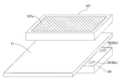
- the lower surfaces of the three semiconductor elements 2 are connected to one P potential metal heat sink 106 a via the bonding material 8.
- the upper end surface 4 c of each of the gate terminals 4 of the three semiconductor elements 2 are connected to one P potential metal heat sink 106 a via the bonding material 8.
- the upper end surface 4 c of each of the gate terminals 4 of the three semiconductor elements 2 on the upper surface of the gate terminals 4 of the three semiconductor elements 2, the upper end surface 5 c of the source terminal 5, and the P potential which also serves as the drain terminal.
- the upper end surface 66c of the metal terminal 66 is exposed from the resin material 10d. As shown in FIG.
- the P potential metal terminal 66 has a columnar portion 66a and an upper end 66b, and the upper end 66b is provided with a projecting portion 66d projecting laterally.
- the shapes of the gate terminal 4 (see FIG. 4) and the source terminal 5 (see FIG. 5) are the same as those in the first embodiment.
- a P potential metal terminal 66 is arranged to surround the gate terminal 4 and the source terminal 5.
- the P potential metal heat sink 106 a is exposed from the resin material 10 d on the lower surface of the power module 106.
- the P potential metal heat radiating plate 106 a and the resin material 10 d are examples of the “heat radiating member” and the “sealing material” in the present invention, respectively.
- the P potential metal terminal 66 is an example of the “conductor for electrode”, the “conductor for second electrode”, the “conductor for second transistor electrode”, and the “conductor for drain electrode” in the present invention.
- the power module 106 is an example of the “power conversion device main unit” in the present invention.
- FIG. 27 In the eighth embodiment, three semiconductor elements 2 constituting an N-side three-phase power module are provided.
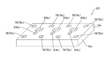
- the power module 107 constitutes an N-side three-phase power module.
- the lower surfaces of the three semiconductor elements 2 are connected to one N-potential metal heat sink 107 a through the bonding material 8.
- the upper end surface 76c of the metal terminal 76 is exposed from the resin material 10e. As shown in FIG.
- the N potential metal terminal 76 has a column-shaped portion 76a and an upper end portion 76b, and the upper end portion 76b is provided with a projecting portion 76d projecting laterally.
- the shape of the gate terminal 4 (see FIG. 4) is the same as that in the first embodiment.
- the N potential metal heat sink 107a is exposed from the resin material 10e on the lower surface of the power module 107.
- the N potential metal heat radiating plate 107a and the resin material 10e are examples of the "heat radiating member" and the "sealing material” in the present invention, respectively.
- the N potential metal terminal 76 is an example of the “conductor for electrode” or the “conductor for second electrode” in the present invention.
- the power module 107 is an example of the “power conversion device main unit” in the present invention.
- the ninth embodiment A ninth embodiment will now be described with reference to FIGS. 30 and 31.
- a P-side three-phase power module 106 according to the seventh embodiment and an N-side three-phase power module 107 according to the eighth embodiment are provided.
- the P-side three-phase power module 106 is provided on the lower surface of the wiring substrate 21, and the N-side three-phase on the upper surface of the wiring substrate 21.
- a power module 107 is provided. Further, the source terminal 5 of the power module 106 is connected to the drain terminal 6 of the power module 107 via the wiring 34 provided inside the wiring substrate 21.
- the P-side metal terminal 32 and the P-side control signal terminal 35 are provided on the lower surface of the wiring board 21, and the N-side metal terminal 33 and the N-side control signal terminal 36 are provided on the upper surface.
- the tenth embodiment differs from the first embodiment in which the semiconductor element 2 and the semiconductor element 3 are provided on the surface of the drain electrode heat sink 1 consisting of only one metal plate, on the surface of the insulating circuit board 109a. The semiconductor element 2 and the semiconductor element 3 are joined.
- the semiconductor element 2 and the semiconductor element 3 are bonded on the surface of the insulating circuit board 109a via the bonding material 8.
- the insulating circuit board 109a has a structure in which a metal plate is attached to both sides of an insulator such as ceramics. The heat generated from the semiconductor element 2 and the semiconductor element 3 is dissipated upward from the gate terminal 4, the source terminal 5, the drain terminal 6 and the anode terminal 7, and is also dissipated from below the insulating circuit board 109 a Is configured.
- the insulating circuit board 109 a is an example of the “heat dissipation member” in the present invention.
- the power module 109 is an example of the “power conversion device main unit” in the present invention.
- the remaining structure of the tenth embodiment is similar to that of the aforementioned first embodiment.
- the outer surface is formed of the resin material 10
- the outer surface is formed of the case-like lower heat spreader 109b and the case-like upper heat spreader 109c.
- the case-like lower heat spreader 109b and the case-like upper heat spreader 109c are made of a metal having conductivity and thermal conductivity.
- the semiconductor element 2, the semiconductor element 3 and the drain terminal 6 are joined on the surface of the insulating circuit board 109a via the joining material 8. ing. Further, on the surface of the semiconductor element 2, the gate terminal 4 and the source terminal 5 are bonded via the bonding material 8. Further, on the surface of the semiconductor element 3, the anode terminal 7 is bonded via the bonding material 8.
- the power module 110 is an example of the “power conversion device main unit” in the present invention.
- a lower heat spreader 109b having a heat dissipation function is disposed on the lower surface of the insulating circuit board 109a.
- the lower heat spreader 109b is formed in a box shape (case shape) having a bottom surface and a side surface.
- the upper heat spreader 109 c is disposed on the lower heat spreader 109 b via the bonding material 8.
- the upper heat spreader 109c is formed in a box shape (case shape) having an upper surface and a side surface. Further, as shown in FIG. 37, an opening 109d is provided on the upper surface of the upper heat spreader 109c.
- the semiconductor element 2 and the semiconductor element 3 are housed inside the lower heat spreader 109 b and the upper heat spreader 109 c.
- the lower heat spreader 109 b and the upper heat spreader 109 c are examples of the “case portion” in the present invention.
- resin injection holes 109e are provided on the side surfaces of the lower heat spreader 109b and the upper heat spreader 109c. Then, by injecting the resin from the resin injection hole 109e, the space between the lower heat spreader 109b and the upper heat spreader 109c, and the semiconductor element 2 and the semiconductor element 3 is filled with the resin material 10f.
- the upper end surface 4c of the gate terminal 4, the upper end surface 5c of the source terminal 5, the upper end surface 6c of the drain terminal 6, and the upper end surface 7c of the anode terminal 7 are from the upper surface of the resin material 10f (the opening 109d of the upper heat spreader 109c). It is configured to be exposed.
- the side surfaces of the semiconductor element 2, the semiconductor element 3, the gate terminal 4, the source terminal 5, the drain terminal 6, and the anode terminal 7 are covered and the upper end surface 4 c of the gate terminal 4,
- the lower heat spreader 109 b and the upper heat spreader 109 c are filled with the resin material 10 f so as to expose the upper end face 5 c of the source terminal 5, the upper end face 6 c of the drain terminal 6 and the upper end face 7 c of the anode terminal 7.
- the semiconductor element 2, the semiconductor element 3, the gate terminal 4, the source terminal 5, the drain terminal 6, and the anode terminal 7 are covered with the resin material 10f, and the resin material 10f further includes the lower heat spreader 109b and the upper heat spreader 109c. Because the semiconductor device 2 and the semiconductor device 3 are damaged by external impact, damage to the semiconductor device 2 and the semiconductor device 3 can be further suppressed.
- the present invention is not limited thereto. It is not limited. In the present invention, at least one substantially flat upper end surface of the gate terminal, the source terminal, the drain terminal and the anode terminal (cathode terminal) may be exposed from the resin material.
- the substantially flat upper end surfaces of the gate terminal, the source terminal, the drain terminal, and the anode terminal have the same height, but the present invention is not limited thereto. It is not limited to.
- the heights of the substantially flat upper end faces of the gate terminal, the source terminal, the drain terminal, and the anode terminal may be different from each other.
- the gate terminal, the source terminal, the drain terminal, and the anode terminal have an example having a pillar-shaped portion, but the present invention is not limited to this.
- the gate terminal, the source terminal, the drain terminal, and the anode terminal may have pillars other than the pillar shape.
- the substantially flat upper end surfaces of the gate terminal, the source terminal, the drain terminal, and the anode terminal have substantially the same height as the upper surface of the resin material.
- the present invention is not limited to this.
- substantially flat upper end surfaces of the gate terminal, the source terminal, the drain terminal, and the anode terminal (cathode terminal) may protrude from the upper surface of the resin material.
- the drain terminal is separated from the gate terminal, the source terminal, and the anode terminal.
- the present invention is not limited to this.
- the gate terminal, the source terminal, the drain terminal, and the anode terminal may be close to each other.
- the protruding portions of the upper end portions of the drain terminal, the gate terminal, the source terminal, and the anode terminal are provided so as to circumferentially protrude from the outer peripheral surface of the columnar portion.
- the present invention is not limited to this.
- the protrusion may be provided on only one side of the column-shaped portion.
- the projecting portion may be circumferentially provided on a part of the outer peripheral surface of the column-shaped portion.
- the protrusions are provided at the upper end portions of the drain terminal, the gate terminal, the source terminal, and the anode terminal, but the present invention is not limited to this. In the present invention, the protrusion may be provided only on the upper end of any one of the drain terminal, the gate terminal, the source terminal, and the anode terminal.
- a high frequency switchable FET is formed on a SiC substrate containing silicon carbide (SiC) as a main component as a semiconductor element. It is not limited to.
- a semiconductor element a high-frequency switchable FET formed on a GaN substrate containing gallium nitride (GaN) as a main component may be used.
- a MOSFET metal oxide film type field effect transistor
- Si Si substrate containing silicon
- IGBT insulated gate bipolar transistor
- the fast recovery diode is used as the freewheeling diode element.
- the present invention is not limited to this.
- a Schottky barrier diode may be used as the free wheeling diode element.
- other diode elements other than the fast recovery diode (FRD) and the Schottky barrier diode (SBD) may be used.
- the bonding material includes Au-20Sn, Zn-30Sn, Pb-5Sn, organic layer-coated nano Ag particles, etc., but the present invention is limited thereto. Absent.
- solder foil or cream solder may be used as a bonding material.
Landscapes
- Cooling Or The Like Of Semiconductors Or Solid State Devices (AREA)
- Inverter Devices (AREA)
- Electrodes Of Semiconductors (AREA)
Abstract
Description
まず、図1~図10を参照して、本発明の第1実施形態によるパワーモジュール100の構成について説明する。なお、第1実施形態では、本発明の電力変換装置をパワーモジュール100に適用する場合について説明する。なお、パワーモジュール100は、本発明の「電力変換装置本体部」の一例である。
次に、図11を参照して、第2実施形態について説明する。この第2実施形態では、上記第1実施形態のパワーモジュール100(パワーモジュール本体部100aおよび100b)が配線基板21に取り付けられている。なお、パワーモジュール本体部100aおよび100bは、本発明の「電力変換装置本体部」の一例である。
次に、図12を参照して、第3実施形態について説明する。この第3実施形態では、上記パワーモジュール本体部100aおよび100bが配線基板21の表面上に隣接するように配置されていた上記第2実施形態と異なり、パワーモジュール本体部100aおよび100bが配線基板21の両面に配置されている。
次に、図13を参照して、第4実施形態について説明する。この第4実施形態では、上記半導体素子2および半導体素子3が1つずつ設けられる上記第1実施形態と異なり、半導体素子2および半導体素子3を一対(2つ)ずつ設ける。
次に、図14~図18を参照して、第5実施形態について説明する。この第5実施形態では、上記半導体素子2および半導体素子3が設けられる上記第1実施形態と異なり、半導体素子2のみ、設けられている。
次に、図19~図23を参照して、第6実施形態について説明する。この第6実施形態では、上記半導体素子2および半導体素子3が設けられる上記第1実施形態と異なり、半導体素子3のみ、設けられている
次に、図24~図26を参照して、第7実施形態について説明する。この第7実施形態では、上記1つの半導体素子2および1つの半導体素子3が設けられる上記第1実施形態と異なり、P側3相のパワーモジュールを構成する3つの半導体素子2が設けられている。
次に、図27~図29を参照して、第8実施形態について説明する。この第8実施形態では、N側3相のパワーモジュールを構成する3つの半導体素子2が設けられている。
次に、図30および図31を参照して、第9実施形態について説明する。この第9実施形態では、上記第7実施形態によるP側3相のパワーモジュール106と、上記第8実施形態によるN側3相のパワーモジュール107とが設けられている。
次に、図32~図34を参照して、第10実施形態について説明する。この第10実施形態では、上記1枚の金属板のみからなるドレイン電極放熱板1の表面上に半導体素子2および半導体素子3が設けられる第1実施形態と異なり、絶縁回路基板109aの表面上に半導体素子2および半導体素子3が接合されている。
次に、図35~図39を参照して、第11実施形態について説明する。この第11実施形態では、上記樹脂材10により外形面が形成されている第1実施形態と異なり、外形面が、ケース状の下側ヒートスプレッダ109bおよびケース状の上側ヒートスプレッダ109cにより形成されている。なお、ケース状の下側ヒートスプレッダ109bおよびケース状の上側ヒートスプレッダ109cは、導電性および熱伝導性を有する金属からなる。
Claims (20)
- 電極を有する電力変換用半導体素子と、
前記電力変換用半導体素子の電極に電気的に接続され、側面と略平坦な上端面を有する上端部とを含む電極用導体と、
前記電力変換用半導体素子と前記電極用導体の側面とを覆う樹脂からなる封止材とを備え、
前記封止材は、前記封止材の上面において、前記電極用導体の略平坦な上端面を露出させるとともに、露出された前記電極用導体の略平坦な上端面を有する上端部には、側方に突出する突出部が設けられている、電力変換装置。 - 前記電極用導体は、上方に延びる柱形状を有し、
前記電極用導体の上端部の前記突出部は、柱形状の前記電極用導体の外周面から周状に突出するように設けられている、請求項1に記載の電力変換装置。 - 前記電極用導体は、複数設けられており、
前記突出部が設けられた複数の前記電極用導体の略平坦な上端面は、互いに略同じ高さを有する、請求項1または2に記載の電力変換装置。 - 前記突出部が設けられた前記電極用導体の略平坦な上端面は、前記封止材の上面と略同じ高さを有する、請求項1に記載の電力変換装置。
- 前記封止材の上面に露出された前記電極用導体の上端面において、外部との電気的接続が行われるように構成されている、請求項1~4のいずれか1項に記載の電力変換装置。
- 前記電力変換用半導体素子の電極は、前記電力変換用半導体素子の主表面に設けられた表面電極と、前記電力変換用半導体素子の裏面に設けられた裏面電極とを含み、
前記電極用導体は、
前記電力変換用半導体素子の主表面において前記表面電極に接合材を介して接続された状態で上方に延びるとともに、前記封止材から露出される略平坦な上端面と前記突出部とを有する第1電極用導体と、
前記電力変換用半導体素子の裏面の前記裏面電極に電気的に接続された状態で前記電力変換用半導体素子から離間した位置から上方に延びるとともに、前記封止材から露出される略平坦な上端面と前記突出部とを有する第2電極用導体とを含む、請求項1~5のいずれか1項に記載の電力変換装置。 - 前記電力変換用半導体素子は、制御電極と第1電極と第2電極とを有する電圧駆動型トランジスタ素子を含み、
前記第1電極用導体は、前記電圧駆動型トランジスタ素子の主表面において、前記制御電極および前記第1電極の少なくともいずれかからなる前記表面電極に前記接合材を介して接続された状態で、上方に延びるとともに、前記略平坦な上端面と前記突出部とを有する第1トランジスタ電極用導体を含み、
前記第2電極用導体は、前記電力変換用半導体素子の裏面の前記第2電極からなる前記裏面電極に電気的に接続された状態で、前記電圧駆動型トランジスタ素子から離間した位置から上方に延びるとともに、前記略平坦な上端面と前記突出部とを有する第2トランジスタ電極用導体を含み、
前記封止材は、前記電圧駆動型トランジスタ素子と、前記第1トランジスタ電極用導体および前記第2トランジスタ電極用導体の側面とを覆うとともに、前記封止材の上面において、前記第1トランジスタ電極用導体および前記第2トランジスタ電極用導体の略平坦な上端面を露出させるように形成されている、請求項6に記載の電力変換装置。 - 前記第1電極はソース電極であり、前記第2電極はドレイン電極であり、
前記第1トランジスタ電極用導体は、前記電圧駆動型トランジスタ素子の主表面において前記制御電極および前記ソース電極にそれぞれ接続され、上方に延びるとともに、前記略平坦な上端面と前記突出部とを有する制御電極用導体およびソース電極用導体を含み、
前記第2トランジスタ電極用導体は、前記電力変換用半導体素子の裏面の前記ドレイン電極に電気的に接続された状態で、前記電圧駆動型トランジスタ素子から離間した位置から上方に延びるとともに、前記略平坦な上端面と前記突出部とを有するドレイン電極用導体を含む、請求項7に記載の電力変換装置。 - 前記封止材は、前記ソース電極用導体の側面を取り囲むように覆うとともに、前記ドレイン電極用導体の側面の少なくとも一部を覆うように形成されており、
前記制御電極用導体、前記ソース電極用導体および前記ドレイン電極用導体の前記略平坦な上端面は、前記封止材から露出されるように形成されている、請求項8に記載の電力変換装置。 - 前記電圧駆動型トランジスタ素子と前記電極用導体と前記樹脂からなる封止材とを含む電力変換装置本体部をさらに備え、
前記ドレイン電極用導体は、前記電力変換装置本体部の端部近傍に配置されている、請求項8または9に記載の電力変換装置。 - 前記電力変換用半導体素子は、第1ダイオード電極および第2ダイオード電極とを有する還流ダイオード素子をさらに含み、
前記第1電極用導体は、前記還流ダイオード素子の主表面において前記第1ダイオード電極からなる前記表面電極に前記接合材を介して接続された状態で、上方に延びるとともに、前記略平坦な上端面を有する第1ダイオード電極用導体を含み、
前記第2電極用導体は、前記還流ダイオード素子の裏面の前記第2ダイオード電極からなる前記裏面電極に電気的に接続された状態で、前記還流ダイオード素子から離間した位置から上方に延びるとともに、前記略平坦な上端面を有する第2ダイオード電極用導体を含み、
前記封止材は、前記還流ダイオード素子と、前記第1ダイオード電極用導体および前記第2ダイオード電極用導体の側面とを覆うとともに、前記封止材の上面において、前記第1ダイオード電極用導体および前記第2ダイオード電極用導体の略平坦な上端面を露出させるように形成されている、請求項6~10のいずれか1項に記載の電力変換装置。 - 前記電力変換用半導体素子と前記電極用導体と前記樹脂からなる封止材とを含む電力変換装置本体部をさらに備え、
前記封止材は、電力変換装置本体部の外形面を構成するように設けられている、請求項1~11のいずれか1項に記載の電力変換装置。 - 前記電力変換用半導体素子および前記電極用導体を取り囲むように設けられたケース部をさらに備え、
前記封止材は、前記電力変換用半導体素子と前記電極用導体の側面とを覆うとともに、前記電極用導体の上端面を露出させるように、前記ケース部内に充填されている、請求項1~12のいずれか1項に記載の電力変換装置。 - 前記電力変換用半導体素子の裏面側に配置された放熱部材をさらに備え、
前記電力変換用半導体素子の主表面側に配置された電極用導体の略平坦な上端面と、前記電力変換用半導体素子の裏面側に配置された放熱部材との両方から前記電力変換用半導体素子で発生した熱を放熱可能なように構成されている、請求項1~13のいずれか1項に記載の電力変換装置。 - 前記放熱部材は、前記電力変換用半導体素子の裏面に接合材を介して接合されている、請求項14に記載の電力変換装置。
- 前記放熱部材は、絶縁物を含まない金属板により構成されている、請求項14または15に記載の電力変換装置。
- 前記封止材は、前記放熱部材を取り囲むとともに前記放熱部材の表面を露出させるように配置されている、請求項14~16のいずれか1項に記載の電力変換装置。
- 前記電力変換用半導体素子は、SiCまたはGaNからなる半導体により形成されている、請求項1~17のいずれか1項に記載の電力変換装置。
- 前記封止材の上面から露出された前記電極用導体の上端面は、配線基板に電気的に接続されている、請求項1~18のいずれか1項に記載の電力変換装置。
- 前記封止材の上面から露出された前記電極用導体の上端面は、配線基板とバンプ電極により電気的に接続されている、請求項19に記載の電力変換装置。
Priority Applications (3)
| Application Number | Priority Date | Filing Date | Title |
|---|---|---|---|
| JP2011519849A JPWO2010147201A1 (ja) | 2009-06-19 | 2010-06-18 | 電力変換装置 |
| CN2010800270049A CN102460694A (zh) | 2009-06-19 | 2010-06-18 | 电力变换装置 |
| US13/851,208 US20130207121A1 (en) | 2009-06-19 | 2013-03-27 | Power conversion device |
Applications Claiming Priority (4)
| Application Number | Priority Date | Filing Date | Title |
|---|---|---|---|
| JP2009-146953 | 2009-06-19 | ||
| JP2009146952 | 2009-06-19 | ||
| JP2009-146952 | 2009-06-19 | ||
| JP2009146953 | 2009-06-19 |
Related Child Applications (1)
| Application Number | Title | Priority Date | Filing Date |
|---|---|---|---|
| US201113329379A Continuation | 2009-06-19 | 2011-12-19 |
Publications (1)
| Publication Number | Publication Date |
|---|---|
| WO2010147201A1 true WO2010147201A1 (ja) | 2010-12-23 |
Family
ID=43356516
Family Applications (1)
| Application Number | Title | Priority Date | Filing Date |
|---|---|---|---|
| PCT/JP2010/060335 Ceased WO2010147201A1 (ja) | 2009-06-19 | 2010-06-18 | 電力変換装置 |
Country Status (4)
| Country | Link |
|---|---|
| US (1) | US20130207121A1 (ja) |
| JP (1) | JPWO2010147201A1 (ja) |
| CN (1) | CN102460694A (ja) |
| WO (1) | WO2010147201A1 (ja) |
Cited By (11)
| Publication number | Priority date | Publication date | Assignee | Title |
|---|---|---|---|---|
| CN102903755A (zh) * | 2011-07-27 | 2013-01-30 | 三星电子株式会社 | 功率半导体器件 |
| JP2013157346A (ja) * | 2012-01-26 | 2013-08-15 | Jtekt Corp | 半導体装置 |
| CN103325752A (zh) * | 2012-03-21 | 2013-09-25 | 英飞凌科技股份有限公司 | 电路封装、电子电路封装和用于包封电子电路的方法 |
| JP2014120638A (ja) * | 2012-12-18 | 2014-06-30 | Rohm Co Ltd | パワーモジュール半導体装置およびその製造方法 |
| JP2014157927A (ja) * | 2013-02-15 | 2014-08-28 | Denso Corp | 半導体装置及びその製造方法 |
| JP2016009819A (ja) * | 2014-06-26 | 2016-01-18 | 三菱電機株式会社 | パワー半導体モジュールおよびその製造方法 |
| JP2016100479A (ja) * | 2014-11-21 | 2016-05-30 | 株式会社デンソー | 半導体装置及びパワーモジュール |
| JP2019021680A (ja) * | 2017-07-12 | 2019-02-07 | トヨタ自動車株式会社 | 半導体装置の製造方法 |
| WO2021191946A1 (ja) * | 2020-03-23 | 2021-09-30 | 太陽誘電株式会社 | パワーモジュール |
| KR20240021418A (ko) * | 2022-08-10 | 2024-02-19 | 주식회사 세미파워렉스 | 양면냉각 반도체 모듈 |
| WO2025203906A1 (ja) * | 2024-03-26 | 2025-10-02 | 三菱電機株式会社 | 電力用半導体装置及び電力用半導体装置の製造方法 |
Families Citing this family (7)
| Publication number | Priority date | Publication date | Assignee | Title |
|---|---|---|---|---|
| JP2015162609A (ja) * | 2014-02-27 | 2015-09-07 | 株式会社東芝 | 半導体装置 |
| KR101755769B1 (ko) * | 2014-10-29 | 2017-07-07 | 현대자동차주식회사 | 양면 냉각 파워 모듈 및 이의 제조 방법 |
| EP3032581B1 (de) * | 2014-12-11 | 2019-10-09 | Dr. Johannes Heidenhain GmbH | Schaltzellenanordnung für Wechselrichter |
| JP6874467B2 (ja) * | 2017-03-29 | 2021-05-19 | 株式会社デンソー | 半導体装置とその製造方法 |
| JP7137558B2 (ja) * | 2017-04-24 | 2022-09-14 | ローム株式会社 | 半導体装置 |
| JP6999462B2 (ja) * | 2018-03-26 | 2022-01-18 | 日立Astemo株式会社 | パワー半導体装置 |
| JP7355707B2 (ja) * | 2020-05-13 | 2023-10-03 | 日立Astemo株式会社 | 半導体装置、バスバー及び電力変換装置 |
Citations (3)
| Publication number | Priority date | Publication date | Assignee | Title |
|---|---|---|---|---|
| JP2002252318A (ja) * | 2001-02-27 | 2002-09-06 | Nec Kansai Ltd | チップ型半導体装置 |
| JP2006120970A (ja) * | 2004-10-25 | 2006-05-11 | Toyota Motor Corp | 半導体モジュールとその製造方法 |
| JP2010129818A (ja) * | 2008-11-28 | 2010-06-10 | Mitsubishi Electric Corp | 半導体装置の製造方法および半導体装置 |
Family Cites Families (10)
| Publication number | Priority date | Publication date | Assignee | Title |
|---|---|---|---|---|
| JPH06132424A (ja) * | 1992-10-16 | 1994-05-13 | Fuji Electric Co Ltd | スイッチング半導体装置 |
| JP4408475B2 (ja) * | 1999-02-23 | 2010-02-03 | 三洋電機株式会社 | ボンディングワイヤを採用しない半導体装置 |
| JP3971568B2 (ja) * | 1999-11-29 | 2007-09-05 | 松下電器産業株式会社 | 半導体パッケージ及び半導体パッケージの製造方法 |
| JP3855726B2 (ja) * | 2001-10-23 | 2006-12-13 | 松下電器産業株式会社 | パワーモジュール |
| JP3759131B2 (ja) * | 2003-07-31 | 2006-03-22 | Necエレクトロニクス株式会社 | リードレスパッケージ型半導体装置とその製造方法 |
| WO2006058030A2 (en) * | 2004-11-23 | 2006-06-01 | Siliconix Incorporated | Semiconductor package including die interposed between cup-shaped lead frame and lead frame having mesas and valleys |
| JP4680816B2 (ja) * | 2006-03-31 | 2011-05-11 | 三菱電機株式会社 | 半導体装置 |
| JP4826426B2 (ja) * | 2006-10-20 | 2011-11-30 | 株式会社デンソー | 半導体装置 |
| JP4376890B2 (ja) * | 2006-12-04 | 2009-12-02 | イビデン株式会社 | 半導体チップ実装用回路基板 |
| JP2009043820A (ja) * | 2007-08-07 | 2009-02-26 | Rohm Co Ltd | 高効率モジュール |
-
2010
- 2010-06-18 CN CN2010800270049A patent/CN102460694A/zh active Pending
- 2010-06-18 WO PCT/JP2010/060335 patent/WO2010147201A1/ja not_active Ceased
- 2010-06-18 JP JP2011519849A patent/JPWO2010147201A1/ja active Pending
-
2013
- 2013-03-27 US US13/851,208 patent/US20130207121A1/en not_active Abandoned
Patent Citations (3)
| Publication number | Priority date | Publication date | Assignee | Title |
|---|---|---|---|---|
| JP2002252318A (ja) * | 2001-02-27 | 2002-09-06 | Nec Kansai Ltd | チップ型半導体装置 |
| JP2006120970A (ja) * | 2004-10-25 | 2006-05-11 | Toyota Motor Corp | 半導体モジュールとその製造方法 |
| JP2010129818A (ja) * | 2008-11-28 | 2010-06-10 | Mitsubishi Electric Corp | 半導体装置の製造方法および半導体装置 |
Cited By (14)
| Publication number | Priority date | Publication date | Assignee | Title |
|---|---|---|---|---|
| CN102903755A (zh) * | 2011-07-27 | 2013-01-30 | 三星电子株式会社 | 功率半导体器件 |
| JP2013157346A (ja) * | 2012-01-26 | 2013-08-15 | Jtekt Corp | 半導体装置 |
| US11189537B2 (en) | 2012-03-21 | 2021-11-30 | Infineon Technologies Ag | Circuit package, an electronic circuit package, and methods for encapsulating an electronic circuit |
| CN103325752A (zh) * | 2012-03-21 | 2013-09-25 | 英飞凌科技股份有限公司 | 电路封装、电子电路封装和用于包封电子电路的方法 |
| DE102013102893B4 (de) * | 2012-03-21 | 2018-01-25 | Infineon Technologies Ag | Verfahren zum Verkapseln eines elektronischen Schaltkreises |
| JP2014120638A (ja) * | 2012-12-18 | 2014-06-30 | Rohm Co Ltd | パワーモジュール半導体装置およびその製造方法 |
| JP2014157927A (ja) * | 2013-02-15 | 2014-08-28 | Denso Corp | 半導体装置及びその製造方法 |
| JP2016009819A (ja) * | 2014-06-26 | 2016-01-18 | 三菱電機株式会社 | パワー半導体モジュールおよびその製造方法 |
| JP2016100479A (ja) * | 2014-11-21 | 2016-05-30 | 株式会社デンソー | 半導体装置及びパワーモジュール |
| JP2019021680A (ja) * | 2017-07-12 | 2019-02-07 | トヨタ自動車株式会社 | 半導体装置の製造方法 |
| WO2021191946A1 (ja) * | 2020-03-23 | 2021-09-30 | 太陽誘電株式会社 | パワーモジュール |
| KR20240021418A (ko) * | 2022-08-10 | 2024-02-19 | 주식회사 세미파워렉스 | 양면냉각 반도체 모듈 |
| KR102755762B1 (ko) | 2022-08-10 | 2025-01-21 | 주식회사 세미파워렉스 | 양면냉각 반도체 모듈 |
| WO2025203906A1 (ja) * | 2024-03-26 | 2025-10-02 | 三菱電機株式会社 | 電力用半導体装置及び電力用半導体装置の製造方法 |
Also Published As
| Publication number | Publication date |
|---|---|
| US20130207121A1 (en) | 2013-08-15 |
| CN102460694A (zh) | 2012-05-16 |
| JPWO2010147201A1 (ja) | 2012-12-06 |
Similar Documents
| Publication | Publication Date | Title |
|---|---|---|
| JP5678884B2 (ja) | 電力変換装置 | |
| JPWO2010147201A1 (ja) | 電力変換装置 | |
| US8537550B2 (en) | Wiring board and power conversion device | |
| CN104303297B (zh) | 电力用半导体模块 | |
| US9762140B2 (en) | Semiconductor device | |
| WO2010147202A1 (ja) | 電力変換装置 | |
| US10903138B2 (en) | Semiconductor device and method of manufacturing the same | |
| US12100631B2 (en) | Semiconductor device | |
| JP2002141463A (ja) | 半導体モジュール | |
| CN100533764C (zh) | 半导体装置的模块结构 | |
| US11315850B2 (en) | Semiconductor device | |
| JP6354674B2 (ja) | 半導体装置 | |
| CN106972001A (zh) | 半导体模块以及半导体装置 | |
| US10083935B2 (en) | Semiconductor device and a manufacturing method of the semiconductor device | |
| CN116913904A (zh) | 半导体模块 | |
| JP2023134143A (ja) | 半導体モジュール、半導体装置、及び車両 | |
| US20200266130A1 (en) | Semiconductor device | |
| US20250301761A1 (en) | Semiconductor device | |
| JP2021141237A (ja) | 半導体装置 | |
| KR101897639B1 (ko) | 파워 모듈 | |
| US20250112143A1 (en) | Semiconductor device, semiconductor module and manufacturing method | |
| JP2021174885A (ja) | 半導体モジュール及び半導体モジュールの製造方法 | |
| US20240297100A1 (en) | Semiconductor module, semiconductor device, and vehicle | |
| JP2003347507A (ja) | 半導体パワーデバイス | |
| JP2024166626A (ja) | 半導体モジュール、および半導体モジュールの製造方法 |
Legal Events
| Date | Code | Title | Description |
|---|---|---|---|
| WWE | Wipo information: entry into national phase |
Ref document number: 201080027004.9 Country of ref document: CN |
|
| 121 | Ep: the epo has been informed by wipo that ep was designated in this application |
Ref document number: 10789574 Country of ref document: EP Kind code of ref document: A1 |
|
| WWE | Wipo information: entry into national phase |
Ref document number: 2011519849 Country of ref document: JP |
|
| NENP | Non-entry into the national phase |
Ref country code: DE |
|
| 122 | Ep: pct application non-entry in european phase |
Ref document number: 10789574 Country of ref document: EP Kind code of ref document: A1 |