WO2010113708A1 - 太陽電池モジュールの製造方法 - Google Patents
太陽電池モジュールの製造方法 Download PDFInfo
- Publication number
- WO2010113708A1 WO2010113708A1 PCT/JP2010/055013 JP2010055013W WO2010113708A1 WO 2010113708 A1 WO2010113708 A1 WO 2010113708A1 JP 2010055013 W JP2010055013 W JP 2010055013W WO 2010113708 A1 WO2010113708 A1 WO 2010113708A1
- Authority
- WO
- WIPO (PCT)
- Prior art keywords
- electrode layer
- film
- solar cell
- back electrode
- cell module
- Prior art date
- Legal status (The legal status is an assumption and is not a legal conclusion. Google has not performed a legal analysis and makes no representation as to the accuracy of the status listed.)
- Ceased
Links
Images




Classifications
-
- H—ELECTRICITY
- H10—SEMICONDUCTOR DEVICES; ELECTRIC SOLID-STATE DEVICES NOT OTHERWISE PROVIDED FOR
- H10F—INORGANIC SEMICONDUCTOR DEVICES SENSITIVE TO INFRARED RADIATION, LIGHT, ELECTROMAGNETIC RADIATION OF SHORTER WAVELENGTH OR CORPUSCULAR RADIATION
- H10F71/00—Manufacture or treatment of devices covered by this subclass
- H10F71/138—Manufacture of transparent electrodes, e.g. transparent conductive oxides [TCO] or indium tin oxide [ITO] electrodes
-
- H—ELECTRICITY
- H10—SEMICONDUCTOR DEVICES; ELECTRIC SOLID-STATE DEVICES NOT OTHERWISE PROVIDED FOR
- H10F—INORGANIC SEMICONDUCTOR DEVICES SENSITIVE TO INFRARED RADIATION, LIGHT, ELECTROMAGNETIC RADIATION OF SHORTER WAVELENGTH OR CORPUSCULAR RADIATION
- H10F10/00—Individual photovoltaic cells, e.g. solar cells
- H10F10/10—Individual photovoltaic cells, e.g. solar cells having potential barriers
- H10F10/17—Photovoltaic cells having only PIN junction potential barriers
- H10F10/172—Photovoltaic cells having only PIN junction potential barriers comprising multiple PIN junctions, e.g. tandem cells
-
- H—ELECTRICITY
- H10—SEMICONDUCTOR DEVICES; ELECTRIC SOLID-STATE DEVICES NOT OTHERWISE PROVIDED FOR
- H10F—INORGANIC SEMICONDUCTOR DEVICES SENSITIVE TO INFRARED RADIATION, LIGHT, ELECTROMAGNETIC RADIATION OF SHORTER WAVELENGTH OR CORPUSCULAR RADIATION
- H10F19/00—Integrated devices, or assemblies of multiple devices, comprising at least one photovoltaic cell covered by group H10F10/00, e.g. photovoltaic modules
- H10F19/30—Integrated devices, or assemblies of multiple devices, comprising at least one photovoltaic cell covered by group H10F10/00, e.g. photovoltaic modules comprising thin-film photovoltaic cells
- H10F19/31—Integrated devices, or assemblies of multiple devices, comprising at least one photovoltaic cell covered by group H10F10/00, e.g. photovoltaic modules comprising thin-film photovoltaic cells having multiple laterally adjacent thin-film photovoltaic cells deposited on the same substrate
-
- H—ELECTRICITY
- H10—SEMICONDUCTOR DEVICES; ELECTRIC SOLID-STATE DEVICES NOT OTHERWISE PROVIDED FOR
- H10F—INORGANIC SEMICONDUCTOR DEVICES SENSITIVE TO INFRARED RADIATION, LIGHT, ELECTROMAGNETIC RADIATION OF SHORTER WAVELENGTH OR CORPUSCULAR RADIATION
- H10F19/00—Integrated devices, or assemblies of multiple devices, comprising at least one photovoltaic cell covered by group H10F10/00, e.g. photovoltaic modules
- H10F19/30—Integrated devices, or assemblies of multiple devices, comprising at least one photovoltaic cell covered by group H10F10/00, e.g. photovoltaic modules comprising thin-film photovoltaic cells
- H10F19/31—Integrated devices, or assemblies of multiple devices, comprising at least one photovoltaic cell covered by group H10F10/00, e.g. photovoltaic modules comprising thin-film photovoltaic cells having multiple laterally adjacent thin-film photovoltaic cells deposited on the same substrate
- H10F19/35—Structures for the connecting of adjacent photovoltaic cells, e.g. interconnections or insulating spacers
-
- H—ELECTRICITY
- H10—SEMICONDUCTOR DEVICES; ELECTRIC SOLID-STATE DEVICES NOT OTHERWISE PROVIDED FOR
- H10F—INORGANIC SEMICONDUCTOR DEVICES SENSITIVE TO INFRARED RADIATION, LIGHT, ELECTROMAGNETIC RADIATION OF SHORTER WAVELENGTH OR CORPUSCULAR RADIATION
- H10F19/00—Integrated devices, or assemblies of multiple devices, comprising at least one photovoltaic cell covered by group H10F10/00, e.g. photovoltaic modules
- H10F19/80—Encapsulations or containers for integrated devices, or assemblies of multiple devices, having photovoltaic cells
-
- H—ELECTRICITY
- H10—SEMICONDUCTOR DEVICES; ELECTRIC SOLID-STATE DEVICES NOT OTHERWISE PROVIDED FOR
- H10F—INORGANIC SEMICONDUCTOR DEVICES SENSITIVE TO INFRARED RADIATION, LIGHT, ELECTROMAGNETIC RADIATION OF SHORTER WAVELENGTH OR CORPUSCULAR RADIATION
- H10F19/00—Integrated devices, or assemblies of multiple devices, comprising at least one photovoltaic cell covered by group H10F10/00, e.g. photovoltaic modules
- H10F19/80—Encapsulations or containers for integrated devices, or assemblies of multiple devices, having photovoltaic cells
- H10F19/804—Materials of encapsulations
-
- Y—GENERAL TAGGING OF NEW TECHNOLOGICAL DEVELOPMENTS; GENERAL TAGGING OF CROSS-SECTIONAL TECHNOLOGIES SPANNING OVER SEVERAL SECTIONS OF THE IPC; TECHNICAL SUBJECTS COVERED BY FORMER USPC CROSS-REFERENCE ART COLLECTIONS [XRACs] AND DIGESTS
- Y02—TECHNOLOGIES OR APPLICATIONS FOR MITIGATION OR ADAPTATION AGAINST CLIMATE CHANGE
- Y02E—REDUCTION OF GREENHOUSE GAS [GHG] EMISSIONS, RELATED TO ENERGY GENERATION, TRANSMISSION OR DISTRIBUTION
- Y02E10/00—Energy generation through renewable energy sources
- Y02E10/50—Photovoltaic [PV] energy
- Y02E10/548—Amorphous silicon PV cells
Definitions
- the present invention relates to a method for manufacturing a silicon-based thin film type or multi-junction solar cell module. More specifically, the present invention relates to a method for manufacturing a solar cell module that can greatly simplify the manufacturing process of a solar cell module including a barrier film having excellent reliability in various properties such as weather resistance, water resistance, and moisture resistance. .
- solar cells are attracting attention because of the infinite amount of sunlight, which is a resource, and no pollution.
- silicon solar cells such as single crystal silicon, polycrystalline silicon, and amorphous silicon.
- compound solar cells represented by CIS solar cells using a compound made of Cu, In, Ga, Al, Se, S or the like instead of silicon.
- these solar cells are classified into a thin film type, a multi-junction type (tandem type), and the like according to their forms.
- thin-film solar cells, amorphous silicon solar cells, compound solar cells, etc. are relatively low cost, and are easy to increase in area. It has been.
- a fluororesin sheet proposed as a surface protective layer of a solar cell module is rich in plasticity, impact resistance, weight reduction, cost reduction, etc., compared with glass or the like, but heat resistance, water resistance, It is inferior in terms of moisture resistance.
- the filler layer which comprises a solar cell module had the problem that a decomposition product produced
- the barrier layer is provided on the surface of the solar cell element and prevents at least one of water vapor, oxygen gas, decomposition products, or additives from permeating, and the barrier layer.
- a filler layer made of a coating film or a printed film made of a filler composition whose main component is a vehicle, and a filler layer provided on both the front and back surfaces,
- a weathering layer comprising a coating film or a printing film made of a resin composition containing a resin as a main component of the vehicle, and one or more antifouling or ultraviolet shielding layers provided on or between any of the above layers
- a solar cell module characterized by comprising (see, for example, Patent Document 1).
- an electromotive force portion such as a crystalline silicon having a pn junction structure, an amorphous silicon having a pin junction structure, or a compound semiconductor is formed on a substrate such as a glass substrate or a plastic substrate.
- a solar cell element is constituted, and a barrier layer is formed on the surface opposite to the substrate constituting the solar cell element, that is, on the surface of the electromotive force part constituting the solar cell element.
- the barrier layer constituting the invention of Patent Document 1 is a physical vapor deposition method such as a vacuum deposition method or a sputtering method, a chemical vapor deposition method such as a plasma chemical vapor deposition method or a photochemical vapor deposition method, or the like. It is the vapor deposition film
- the object of the present invention is to eliminate solar cells that exhibit stable performance over a long period of time with little reduction in power generation efficiency even in a high humidity environment, eliminating vacuum processes such as vacuum deposition and sputtering as much as possible, and applying wet coating. It is providing the manufacturing method of the solar cell module which can be manufactured more cheaply by using a construction method.
- a first aspect of the present invention includes a step of forming a transparent and conductive surface electrode layer on a substrate, a step of forming one or more photoelectric conversion units that generate power by light on the surface electrode layer, A step of forming a transparent conductive film on the photoelectric conversion unit, a step of forming a back electrode layer on the transparent conductive film, and applying a reinforcing film composition on the back electrode layer by a wet coating method. Forming a back electrode reinforcing film by irradiating or heating the formed layer with ultraviolet rays or heating the ultraviolet rays after ultraviolet irradiation.
- a fourth aspect of the present invention is the invention based on the first aspect, and further, after the step of forming the back electrode reinforcing film, a barrier film composition is applied onto the reinforcing film by a wet coating method.
- the method further comprises a step of forming a barrier film by irradiating the layer obtained by ultraviolet irradiation or heating or heating the layer after ultraviolet irradiation.
- a seventeenth aspect of the present invention includes a step of forming a transparent and conductive surface electrode layer on a substrate, a step of forming one or more photoelectric conversion units that generate power by light on the surface electrode layer, A step of forming a transparent conductive film on the photoelectric conversion unit, a step of forming a back electrode layer on the transparent conductive film, and applying a barrier film composition on the back electrode layer by a wet coating method. And a step of forming a barrier film by irradiating the formed layer with ultraviolet rays or heating, or heating the ultraviolet rays after ultraviolet irradiation.
- 1 or 2 steps of forming a transparent and conductive surface electrode layer on a substrate and a photoelectric conversion unit for generating power by light on the surface electrode layer are provided.
- the step of forming the above, the step of forming a transparent conductive film on the photoelectric conversion unit, the step of forming a back electrode layer on the transparent conductive film, and a relatively simple wet coating of the reinforcing film composition on the back electrode layer And a step of forming a back electrode reinforcing film by irradiating or heating the layer obtained by coating using a coating method or heating the layer after irradiating with ultraviolet rays.
- a back electrode reinforcing film that is hard and dense and has high adhesion to the back electrode layer can be easily obtained in a relatively short time by a wet coating method.
- the back electrode reinforcing film can maintain the electromagnetic characteristics and corrosion resistance of the back electrode layer.
- peeling or chipping occurs in each layer and film after the formation of the separation groove. Can be prevented.
- the back electrode reinforcing film can be formed by a simple method without using expensive and complicated manufacturing equipment with many control items. For this reason, the running cost can be reduced, and even if the module of the solar cell is enlarged, this module can be manufactured relatively easily.
- the barrier film composition was applied onto the reinforcing film by a wet coating method after the step of forming the back electrode reinforcing film.
- the method further includes the step of forming a barrier film by irradiating the layer with ultraviolet rays, heating the layer, or heating the layer after the ultraviolet ray irradiation. Since the barrier film is formed by a wet coating method, a laminated film obtained by intentionally stacking materials having different properties can be obtained. Thereby, the solar cell which has the reliability excellent in various characteristics, such as a weather resistance, water resistance, and moisture resistance, can be manufactured.
- the step of forming a transparent and conductive surface electrode layer on the substrate and one or two photoelectric conversion units for generating power by light on the surface electrode layer are provided.
- the step of forming above, the step of forming a transparent conductive film on the photoelectric conversion unit, the step of forming a back electrode layer on the transparent conductive film, and applying the barrier film composition on the back electrode layer by a wet coating method The layer thus obtained is irradiated with ultraviolet rays, heated, or heated after being irradiated with ultraviolet rays to form a barrier film. Since the barrier film is formed by a wet coating method, a laminated film obtained by intentionally stacking materials having different properties can be obtained. Thereby, the solar cell which has the reliability excellent in various characteristics, such as a weather resistance, water resistance, and moisture resistance, can be manufactured.
- a solar cell module of the present invention vacuum processes such as vacuum deposition and sputtering are eliminated as much as possible, and the wet coating method is used, so that it is cheaper and requires complicated processes.
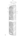
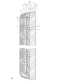
- the thin-film silicon solar cell module 10 includes a substrate 11 having an insulating surface, and a photovoltaic element 15 stacked on the substrate 11.
- the photovoltaic element 15 is formed on the substrate 11 by laminating the front electrode layer 12, the photoelectric conversion unit 13, the transparent conductive film 14, and the back electrode layer 16 in this order.
- the layer obtained by applying the composition for reinforcing film laminated on the photovoltaic element 15 by the wet coating method is irradiated with ultraviolet rays, heated, or heated after being irradiated with ultraviolet rays.
- the photovoltaic element 15, the back electrode reinforcing film 17, the filler layer 19, and the back film 21 are arranged in this order on the back side opposite to the light incident side of the substrate 11.
- the substrate 11 is selected from the group consisting of glass, ceramics, polymer materials, and silicon, or a light-transmitting substrate made of glass, ceramics, or polymer materials. More than one type of translucent laminate can be used.
- the polymer substrate include a substrate formed of an organic polymer such as polyimide or PET (polyethylene terephthalate).
- the surface electrode layer 12 is a transparent and conductive film that transmits light incident from the substrate 11 side to the photoelectric conversion unit 13 and functions as one electrode of the photovoltaic element.
- Examples of the surface electrode layer 12 include ITO (indium oxide-tin oxide composite oxide), ATO (antimony oxide-tin oxide composite oxide), SnO 2 (tin oxide), ZnO (zinc oxide), IZO.
- Examples thereof include films of (indium oxide-zinc oxide composite oxide), AZO (aluminum oxide-zinc oxide composite oxide), and the like.
- the surface electrode layer 12 is made of ZnO, In 2 O 3 , SnO 2 , CdO, TiO 2 , CdIn 2 O 4 , Cd 2 SnO 4 or Zn 2 SnO 4 , Sn, Sb, F, Ga or Al. You may comprise by the 1 type (s) or 2 or more types of metal oxide chosen from the group of the metal oxide which doped any of these.
- the surface electrode layer 12 may be formed by a conventionally known method such as a thermal CVD method, a sputtering method, a vacuum deposition method, or a wet coating method, and is not particularly limited.
- the surface electrode layer 12 When the surface electrode layer 12 is formed by a wet coating method, it is performed in the same manner as when a transparent conductive film 14 described later is formed by a wet coating method.
- the ZnO is suitable as a material for the surface electrode layer 12 because it has high light transmittance, low resistance, and plasticity and is inexpensive.
- the surface electrode layer 12 formed on the substrate 11 by such a method is patterned into a short rail shape by laser scribing. That is, separation processing is performed by forming the separation groove 22.
- the separation groove 22 can be formed using the same apparatus as the separation groove 18 described later.
- the photoelectric conversion unit 13 is composed of an amorphous (amorphous) silicon semiconductor or a crystalline silicon semiconductor.
- the photoelectric conversion unit 13 includes a first photoelectric conversion unit 13a formed of an amorphous silicon semiconductor and a second photoelectric conversion unit 13b formed of a microcrystalline silicon semiconductor.
- the first photoelectric conversion unit 13a includes p-type a-Si (amorphous silicon), i-type a-Si (amorphous silicon), and n-type a-Si (amorphous) in order from the substrate 11 side. This is a pin type amorphous silicon layer in which (quality silicon) is laminated.
- the second photoelectric conversion unit 13b includes p-type ⁇ c-Si (microcrystalline silicon), i-type ⁇ c-Si (microcrystalline silicon), and n-type ⁇ c-Si (microcrystalline silicon) in order from the first photoelectric conversion unit 13a side. ) Is a pin type microcrystalline silicon layer laminated.
- the tandem solar cell module using i-type a-Si (first photoelectric conversion unit 13a) and i-type ⁇ c-Si (second photoelectric conversion unit 13b) as photoelectric conversion units has different light absorption wavelengths. It is a structure in which two types of semiconductors are stacked, and the solar spectrum can be used effectively.
- microcrystal means not only a complete crystal state but also a partially amorphous (amorphous) state.
- the photoelectric conversion unit 13 formed on the surface electrode layer 12 by such a method is patterned into a short rail shape by laser scribing. That is, separation processing is performed by forming the separation groove 23.
- the separation groove 23 can be formed using the same device as the separation groove 18 described later.
- the photoelectric conversion unit is a single junction type including either one of an amorphous silicon layer or a microcrystalline silicon layer, or a multijunction including a plurality of either one or both of an amorphous silicon layer and a microcrystalline silicon layer. It can take any form of mold.
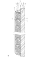
- a structure such as p-type a-SiC: H (amorphous silicon carbide) / i-type a-Si / n-type ⁇ c-Si can be taken. Although they are not particularly limited, they can be formed by a conventionally known method such as a plasma CVD method. Furthermore, between the photoelectric conversion units, for example, in the example of the tandem structure, as shown in FIG. 3, the first photoelectric conversion unit (amorphous silicon photoelectric conversion unit) 13a and the second photoelectric conversion unit 13b (fine An intermediate layer 53a may be formed between the crystalline silicon photoelectric conversion unit) 13b.
- the intermediate layer 53a is preferably made of a material used for the surface electrode layer 12 and the transparent conductive film 14.
- a transparent conductive film 14 is formed on the photoelectric conversion unit 13.
- the transparent conductive film 14 is not particularly limited, but may be formed by a conventionally known method such as sputtering, vacuum deposition, thermal CVD, or wet coating.
- the transparent conductive film 14 is provided to suppress mutual diffusion between the photoelectric conversion unit 13 and the back electrode layer 16 and to increase the reflection efficiency of the back electrode layer 16.
- a transparent conductive film composition is first prepared.
- This composition for transparent conductive films is a composition containing conductive oxide fine particles, and the conductive oxide fine particles are dispersed in a dispersion medium.
- the conductive oxide fine particles contained in the composition for transparent conductive film include ITO (Indium Tin Oxide: indium oxide-tin oxide composite oxide), ATO (Antimony Tin Oxide: antimony oxide-tin oxide composite oxide).
- a tin oxide powder containing one or more metals selected from the group consisting of Al, Co, Fe, In, Sn, Ga and Ti is preferred.
- IZO Indium Zinc ⁇ ⁇ ⁇ ⁇ ⁇ Oxide: indium oxide-zinc oxide composite oxide
- TZO Tin Zinc Oxide: tin-containing zinc oxide composite oxide
- the content of the conductive oxide fine particles in the solid content contained in the transparent conductive film composition is preferably in the range of 50 to 90% by mass.
- the reason why the content of the conductive oxide fine particles is within the above range is that the conductivity is lowered if the content is less than the lower limit, and the adhesiveness is lowered if the upper limit is exceeded.
- a range of 70 to 90% by mass is particularly preferable.
- the average particle diameter of the conductive oxide fine particles is preferably in the range of 10 to 100 nm, and particularly preferably in the range of 20 to 60 nm, in order to maintain stability in the dispersion medium. .
- the composition for transparent conductive film is a composition containing one or both of a polymer-type binder and a non-polymer-type binder that are cured by heating.
- the polymer type binder include acrylic resin, polycarbonate, polyester, alkyd resin, polyurethane, acrylic urethane, polystyrene, polyacetal, polyamide, polyvinyl alcohol, polyvinyl acetate, cellulose, and siloxane polymer.
- Polymeric binders include aluminum, silicon, titanium, zirconium, chromium, manganese, iron, cobalt, nickel, silver, copper, zinc, molybdenum or tin metal soaps, metal complexes or metal alkoxide hydrolysates. It is preferable.
- Non-polymer type binders include metal soaps, metal complexes, metal alkoxides, halosilanes, 2-alkoxyethanol, ⁇ -diketone and alkyl acetate.
- the metal contained in the metal soap, metal complex or metal alkoxide is aluminum, silicon, titanium, zirconium, chromium, manganese, iron, cobalt, nickel, silver, copper, zinc, molybdenum, tin, indium or antimony.
- These polymer-type binder and non-polymer-type binder are cured by heating, thereby enabling formation of the transparent conductive film 14 having a low haze ratio and volume resistivity at low temperatures.
- the content of these binders is preferably in the range of 5 to 50% by mass, particularly preferably in the range of 10 to 30% by mass as a proportion of the solid content in the composition for transparent conductive film.
- a coupling agent to the transparent conductive film composition according to other components to be used. This is for improving the adhesion between the conductive fine particles and the binder and the adhesion between the transparent conductive film 14 formed of the composition for transparent conductive film and the photoelectric conversion unit 13 or the back electrode layer 16.
- the coupling agent include silane coupling agents, aluminum coupling agents, and titanium coupling agents.
- silane coupling agent examples include vinyltriethoxyxysilane, ⁇ -glycidoxypropyltrimethoxysilane, and ⁇ -methacryloxypropyltrimethoxysilane.
- aluminum coupling agent examples include an aluminum coupling agent containing an acetoalkoxy group represented by the following formula (1).
- titanium coupling agent a titanium coupling agent having a dialkyl pyrophosphite group represented by the following formulas (2) to (4), or a titanium having a dialkyl phosphite group represented by the following formula (5): A coupling agent is mentioned.
- the composition for transparent conductive film is applied on the photoelectric conversion unit 13 by a wet coating method, and the thickness after firing is 0.03.
- the film is formed to be in the range of -0.5 ⁇ m, preferably 0.05-0.3 ⁇ m.
- the reason why the thickness of the transparent conductive film 14 is limited to the range of 0.03 to 0.5 ⁇ m is that the effect of increasing reflection cannot be obtained sufficiently if the thickness is less than 0.03 ⁇ m or exceeds 0.5 ⁇ m.
- the transparent conductive film 14 is formed by baking the laminated body in the air or in an inert gas atmosphere such as nitrogen or argon at a temperature of 120 to 400 ° C. for 5 to 60 minutes.
- a back electrode layer 16 is formed on the transparent conductive film 14. Since this back electrode layer 16 plays the role which improves the power generation efficiency by reflecting the light which has not been absorbed and transmitted through the photoelectric conversion unit and returning it to the photoelectric conversion unit again, a high diffuse reflectance is required. For this reason, the back electrode layer 16 is preferably a metal having a high reflectance. Examples of the metal include metals such as silver, iron, chromium, tantalum, molybdenum, nickel, aluminum, cobalt, and titanium, alloys of these metals, and alloys such as nichrome and stainless steel.
- the back electrode layer 16 is not particularly limited, and may be formed by a conventionally known method such as a thermal CVD method, a sputtering method, a vacuum deposition method, or a wet coating method.
- an electrode composition in which metal nanoparticles are dispersed in a dispersion medium is used.
- This composition for electrodes is a composition prepared by dispersing metal nanoparticles in a dispersion medium.
- the ratio of silver in the metal element is 75% by mass or more, preferably 80% by mass or more. The reason why the ratio of silver in the metal element is in the range of 75% by mass or more is that if it is less than 75% by mass, the reflectivity of the back electrode layer 16 formed using this electrode composition is lowered. .
- the metal nanoparticles are chemically modified with a protective agent for an organic molecular main chain having a carbon skeleton of 1 to 3 carbon atoms.
- the carbon skeleton of the organic molecular main chain of the protective agent that chemically modifies the metal nanoparticles is in the range of 1 to 3 because if the carbon number is 4 or more, the protective agent is desorbed or decomposed (separated) by heating. This is because it is difficult to burn), and a large amount of organic residue remains in the back electrode layer 16, and the conductivity and reflectivity of the back electrode layer 16 are lowered due to deterioration or deterioration.
- the metal nanoparticles preferably contain 70% or more, preferably 75% or more of the number average of metal nanoparticles having a primary particle size in the range of 10 to 50 nm.
- the content of the metal nanoparticles in the primary particle size range of 10 to 50 nm is less than 70% by mass with respect to 100% of all the metal nanoparticles on the average, the specific surface area of the metal nanoparticles increases and The proportion occupied is increased. For this reason, even if the organic molecule is easily desorbed or decomposed (separated / combusted) by heating, a large proportion of the organic molecule occupies it, so that a large amount of organic residue remains in the back electrode layer 16.
- the residue may be altered or deteriorated, and the conductivity and reflectance of the back electrode layer 16 may be reduced. Moreover, it is because the particle size distribution of the metal nanoparticles becomes wide and the density of the back electrode layer 16 tends to decrease, and the conductivity and reflectivity of the back electrode layer 16 decrease. Furthermore, from the correlation between the primary particle size and the aging stability of the metal nanoparticles (aging stability), the primary particle size of the metal nanoparticles was set within the range of 10 to 50 nm.
- the electrode composition containing the metal nanoparticles further includes one or more additives selected from the group consisting of organic polymers, metal oxides, metal hydroxides, organometallic compounds, and silicone oils. It is preferable.
- an organic polymer, metal oxide, metal hydroxide, organometallic compound, or silicone oil contained in the electrode composition is used.
- the chemical bond with the substrate or the anchor effect is increased, or the wettability between the metal nanoparticles and the substrate is improved in the process of heating and firing, and the conductivity is not impaired. Adhesiveness can be improved.
- grain growth due to sintering between metal nanoparticles can be adjusted. The formation of the back electrode layer 16 using this electrode composition does not require a vacuum process at the time of film formation, so the process restrictions are small and the running cost of the manufacturing equipment can be greatly reduced.
- the content of the additive is 0.1 to 20%, preferably 0.2 to 10% of the mass of the silver nanoparticles constituting the metal nanoparticles. If the content of the additive is less than 0.1%, pores having a large average diameter may appear or the pore density may be increased. If the content of the additive exceeds 20%, the conductivity of the back electrode layer 16 formed is adversely affected, resulting in a problem that the volume resistivity exceeds 2 ⁇ 10 ⁇ 5 ⁇ ⁇ cm.
- the organic polymer used as the additive one or more selected from the group consisting of polyvinylpyrrolidone (hereinafter referred to as PVP), a PVP copolymer and water-soluble cellulose is used.
- PVP copolymer examples include a PVP-methacrylate copolymer, a PVP-styrene copolymer, and a PVP-vinyl acetate copolymer.
- the water-soluble cellulose include cellulose ethers such as hydroxypropyl methylcellulose, methylcellulose, and hydroxyethylmethylcellulose.
- the metal oxide used as an additive is at least selected from the group consisting of aluminum, silicon, titanium, zirconium, chromium, manganese, iron, cobalt, nickel, silver, copper, zinc, molybdenum, tin, indium and antimony
- An oxide containing one kind or a composite oxide is preferable.
- composite oxides include ITO (Indium Tin Oxide), ATO (Antimony Tin Oxide), IZO (Indium Zic Oxide). Indium-zinc oxide composite oxide), AZO (Aluminum Zinc Oxide: aluminum oxide-zinc oxide composite oxide) and the like.
- the metal hydroxide used as an additive was selected from the group consisting of aluminum, silicon, titanium, zirconium, chromium, manganese, iron, cobalt, nickel, silver, copper, zinc, molybdenum, tin, indium and antimony.
- a hydroxide containing at least one kind is preferred.
- a metal soap containing at least one selected from the group consisting of silicon, titanium, zirconium, chromium, manganese, iron, cobalt, nickel, silver, copper, zinc, molybdenum and tin Metal complexes or metal alkoxides are preferred.
- the metal soap include chromium acetate, manganese formate, iron citrate, cobalt formate, nickel acetate, silver citrate, copper acetate, copper citrate, tin acetate, zinc acetate, zinc oxalate, and molybdenum acetate.
- Examples of the metal complex include an acetylacetone zinc complex, an acetylacetone chromium complex, and an acetylacetone nickel complex.
- Examples of the metal alkoxide include titanium isopropoxide, methyl silicate, isoanatopropyltrimethoxysilane, and aminopropyltrimethoxysilane.
- both straight silicone oil and modified silicone oil can be used.
- the modified silicone oil further has an organic group introduced into part of the side chain of the polysiloxane (side chain type), an organic group introduced into both ends of the polysiloxane (both end type), and both ends of the polysiloxane. Those having an organic group introduced into one of them (one end type) and those having an organic group introduced into a part of both side chains and both ends of the polysiloxane (both side chain end types) can be used.
- the modified silicone oil includes a reactive silicone oil and a non-reactive silicone oil. Both types can be used as the additive of the present invention.
- Reactive silicone oil means amino modification, epoxy modification, carboxy modification, carbinol modification, mercapto modification, and different functional group modification (epoxy group, amino group, polyether group). Indicates polyether modification, methylstyryl group modification, alkyl modification, higher fatty acid ester modification, fluorine modification, and hydrophilic special modification.
- the metal nanoparticles other than silver nanoparticles are composed of gold, platinum, palladium, ruthenium, nickel, copper, tin, indium, zinc, iron, chromium and manganese. It is preferable to further contain metal nanoparticles composed of one kind of particles selected from the group or two or more kinds of mixed compositions or alloy compositions.
- the metal nanoparticles other than the silver nanoparticles are preferably 0.02% by mass or more and less than 25% by mass with respect to 100% by mass of all metal nanoparticles, and 0.03% by mass to 20% by mass. Is more preferable.
- the content of particles other than silver nanoparticles is in the range of 0.02% by mass or more and less than 25% by mass, it is maintained in a constant temperature and humidity chamber having a temperature of 100 ° C. and a humidity of 50% for 1000 hours. This is because the conductivity and reflectance of the back electrode layer 16 after the test) are not deteriorated as compared with those before the weather resistance test.
- the content of the metal nanoparticles including silver nanoparticles in the electrode composition is 2.5 to 95.0% by mass with respect to 100% by mass of the electrode composition comprising the metal nanoparticles and the dispersion medium.
- the content is preferably 3.5 to 90% by mass. This is because if the content ratio with respect to 100% by mass of the electrode composition exceeds 95.0% by mass, the required fluidity as an ink or paste is lost during wet coating of the electrode composition.
- the dispersion medium constituting the electrode composition for forming the back electrode layer 16 is 1% by mass or more, preferably 2% by mass or more of water and 2% by mass with respect to 100% by mass of all the dispersion media.
- a solvent compatible with 3% by mass or more of water for example, alcohols.
- the dispersion medium is composed of only water and alcohols, it contains 98% by mass of alcohol when it contains 2% by mass of water, and 98% by mass of water when it contains 2% by mass of alcohol.
- the dispersion medium that is, the protective molecule chemically modified on the surface of the metal nanoparticle contains either one or both of a hydroxyl group (—OH) and a carbonyl group (—C ⁇ O).
- the water content is preferably in the range of 1% by mass or more with respect to 100% by mass of all the dispersion media. This is because if the water content is less than 2% by mass, it becomes difficult to sinter the film obtained by applying the electrode composition by a wet coating method at a low temperature. Furthermore, the conductivity and reflectance of the back electrode layer 16 after firing are reduced.
- the composition for electrodes is excellent in dispersion stability and effective for low-temperature sintering of the coating film. There is an effect.
- a carbonyl group (—C ⁇ O) is contained in a protective agent that chemically modifies metal nanoparticles such as silver nanoparticles, it is excellent in dispersion stability of the electrode composition as described above, and the coating film has a low temperature. Sintering also has an effective action.
- the solvent compatible with water used for the dispersion medium alcohols are preferable.
- the alcohols it is particularly preferable to use one or more selected from the group consisting of methanol, ethanol, propanol, butanol, ethylene glycol, propylene glycol, diethylene glycol, glycerol, isobornyl hexanol and erythritol. preferable.
- the method for producing an electrode composition containing metal nanoparticles for forming the back electrode layer 16 is as follows.
- the aqueous metal salt solution is added dropwise to and mixed with the reducing agent aqueous solution while stirring the reducing agent aqueous solution in the inert gas stream.
- the concentration of each solution so that the amount of the metal salt aqueous solution added is 1/10 or less of the amount of the reducing agent aqueous solution, the reaction temperature is 30 to 30% even when the metal salt aqueous solution at room temperature is dropped. It is preferable to keep the temperature at 60 ° C.
- the mixing ratio of the two aqueous solutions is adjusted so that the equivalent of ferrous ions added as a reducing agent is three times the equivalent of metal ions.
- the mixture is stirred for an additional 10 to 300 minutes to prepare a dispersion composed of metal colloid.
- This dispersion is allowed to stand at room temperature, and the aggregates of the precipitated metal nanoparticles are separated by decantation, centrifugation, etc., and then water such as deionized water is added to the separation to form a dispersion, followed by ultrafiltration. Demineralize by.
- the metal (silver) content is adjusted to 2.5 to 50 mass%.
- the centrifugal force of the centrifuge is adjusted using a centrifuge to separate coarse particles, whereby the silver nanoparticles having a primary particle diameter in the range of 10 to 50 nm have a number average of 70% or more.
- the ratio of silver nanoparticles in the range of the primary particle diameter of 10 to 50 nm to 100% of all silver nanoparticles is adjusted so that the number average is 70% or more.
- a dispersion in which the carbon skeleton of the carbon skeleton of the organic molecular main chain of the protective agent for chemically modifying the silver nanoparticles is 3 is obtained.
- the obtained dispersion is adjusted so that the final metal content (silver content) with respect to 100% by mass of the dispersion is in the range of 2.5 to 95% by mass.
- the dispersion medium is an alcohol-containing aqueous solution
- the dispersion is one or more selected from the group consisting of organic polymers, metal oxides, metal hydroxides, organometallic compounds, and silicone oils. It is carried out by adding two or more additives in a desired ratio.
- the content of the additive is adjusted to be in the range of 0.1 to 20% by mass with respect to 100% by mass of the obtained electrode composition.
- the metal constituting the metal nanoparticles other than the silver nanoparticles is gold, Examples include platinum, palladium, ruthenium, nickel, copper, tin, indium, zinc, iron, chromium and manganese.
- the silver nitrate used in preparing the aqueous metal salt solution was chloroauric acid, chloroplatinic acid, palladium nitrate, ruthenium trichloride, nickel chloride, cuprous nitrate, tin dichloride, indium nitrate, zinc chloride, iron sulfate, sulfuric acid
- a dispersion is prepared in the same manner as in the above (a) except that it is replaced with chromium or manganese sulfate.
- a dispersion having 3 carbon atoms in the carbon skeleton of the organic molecular main chain of the protective agent that chemically modifies the metal nanoparticles other than the silver nanoparticles is obtained.
- the carbon number of the carbon skeleton of the organic molecular main chain of the protective agent that chemically modifies the metal nanoparticles other than the silver nanoparticles is 1 or 2
- the silver nitrate used when preparing the metal salt aqueous solution is the above kind.
- a dispersion is prepared in the same manner as in the above (b) and (c) except that the metal salt is replaced. Thereby, the dispersion whose carbon number of carbon skeleton of the organic molecular principal chain of the protective agent which chemically modifies metal nanoparticles other than silver nanoparticles is 1 or 2 is obtained.
- the metal nanoparticles include metal nanoparticles other than silver nanoparticles together with silver nanoparticles
- a dispersion containing silver nanoparticles produced by the method of (a) is used as the first dispersion
- the dispersion containing metal nanoparticles other than the silver nanoparticles produced by the method (d) is used as the second dispersion
- 75% by mass or more of the first dispersion and less than 25% by mass of the second dispersion are obtained. Mixing is performed so that the total content of the first and second dispersions is 100% by mass.
- the first dispersion is not limited to the dispersion containing the silver nanoparticles produced by the method (a), but the dispersion containing the silver nanoparticles produced by the method (b) or the above (c). Dispersions containing silver nanoparticles produced by the method may be used.
- the electrode composition is applied onto the photoelectric conversion unit 13 by a wet coating method, and heated to a thickness after firing of 0.05.
- the electrode coating layer is formed so as to have a thickness of ⁇ 2.0 ⁇ m, preferably 0.1 ⁇ 1.5 ⁇ m.
- the electrode coating layer is maintained in the atmosphere or in an inert gas atmosphere such as nitrogen or argon at a temperature of 130 to 400 ° C., preferably 150 to 350 ° C. for 5 minutes to 1 hour, preferably 15 to 40 minutes. And fired.
- the thickness of the back electrode layer 16 after firing was limited to be in the range of 0.05 to 2.0 ⁇ m.
- the heating temperature of the electrode coating layer was set to a range of 130 to 400 ° C. This is because if the temperature is lower than 130 ° C., the metal nanoparticles are not sufficiently sintered and are not easily detached or decomposed (separated / burned) by heating the protective agent. That is, a large amount of organic residue remains in the back electrode layer 16 after firing, and the residue is altered or deteriorated, so that the conductivity and reflectance of the back electrode layer 16 are lowered. Moreover, if it exceeds 400 degreeC, the merit in a low temperature process cannot be utilized.
- the manufacturing cost is increased and the productivity is lowered.
- it affects the light wavelength region of photoelectric conversion in amorphous silicon, microcrystalline silicon, or a hybrid silicon solar cell module using these. It is.
- the heating time of the electrode coating layer was set in the range of 5 minutes to 1 hour. This is because the sintering between the metal nanoparticles becomes insufficient for less than 5 minutes, and it is difficult to desorb or decompose (separate / burn) by heating the protective agent, so that an organic residue is present in the back electrode layer 16 after firing. This is because a large amount of the residue remains, and the residue is altered or deteriorated, and the conductivity and reflectance of the back electrode layer 16 are reduced.
- the back electrode layer 16 is formed by the wet coating method in this way, a simple process can be completed in a short time, and since a vacuum process is not required at the time of film formation, the process restrictions are small and the running cost of the manufacturing equipment is greatly increased. Can be reduced.
- the average diameter of pores appearing on the contact surface on the photoelectric conversion unit 13 side of the layer is 100 nm or less
- the average depth at which the pores are located is 100 nm or less
- the number density of the pores is 30 / ⁇ m 2 or less.
- photoelectric conversion is achieved by reducing the average diameter of the pores appearing on the contact surface of the back electrode layer 16 on the photoelectric conversion unit 13 side, reducing the average depth at which the pores are located, and reducing the number density of the pores.
- the inflection point at which the reflection spectrum measured from the photoelectric conversion unit 13 side starts to decrease when the back electrode layer 16 is formed on the unit 13 is shifted to the short wavelength side.
- the average diameter of pores appearing on the contact surface on the photoelectric conversion unit 13 side of the back electrode layer 16 is 100 nm or less
- the average depth at which the pores are located is 100 nm or less
- the number density of the pores Of 30 pieces / ⁇ m 2 or less is 100 nm or less.
- the back electrode layer 16 has a specific resistance close to the specific resistance of the metal itself constituting the metal nanoparticles contained in the electrode composition. That is, it shows a specific resistance as low as a bulk that can be used as an electrode for a solar cell module.
- the back electrode layer 16 of the present invention is superior in long-term stability such as film reflectivity, adhesion, and specific resistance compared to a film formed by a vacuum process such as sputtering.
- the reason for this is that the back electrode layer 16 of the present invention formed in the atmosphere is less susceptible to moisture intrusion and oxidation than a film formed in vacuum.
- a back electrode reinforcing film 17 is formed on the back electrode layer 16 by a wet coating method.
- the back electrode reinforcing film 17 maintains the electromagnetic characteristics and corrosion resistance of the back electrode layer 16, and prevents the layers and films from being separated or chipped after the separation grooves are formed by laser scribing. is there.
- a reinforcing film composition applied on the back electrode layer 16 by a wet coating method is prepared.
- This reinforcing film composition is made of an organic or inorganic base material of a polymer type binder or an inorganic base material of a non-polymer type binder that is cured by being irradiated with ultraviolet rays, heated, or heated after being irradiated with ultraviolet rays. Either or both of these are included.
- the organic base material of the polymer type binder includes one or more selected from the group consisting of acrylic, epoxy, urethane, acrylic urethane, epoxy acrylic, cellulose and siloxane polymers. Is preferred.
- acrylic binder an acrylic polymer obtained by adding a photopolymerization initiator to an acrylic monomer and irradiating the mixture with ultraviolet rays (UV) to perform photopolymerization is used.
- acrylic monomers include 1,6-hexanediol diacrylate, trimethylolpropane triacrylate, neopentyl glycol diacrylate, tetramethylolmethane tetraacrylate, ditrimethylolpropane tetraacrylate, 1,9-nonanediol diacrylate, and tripropylene.
- Examples thereof include one or two or more single monomers or mixed monomers selected from the group consisting of glycol diacrylate, ethoxylated isocyanuric acid triacrylate, and tetramethylolmethane tetraacrylate.
- a solvent such as MIBK (methyl isobutyl ketone), PGME (1-methoxy-2-propanol), or PGMEA (propylene glycol monomethyl ether acetate) is preferably added to these monomers.
- photopolymerization initiators examples include 1-hydroxy-cyclohexyl-phenyl-ketone, 2-hydroxy-2-methyl-1-phenyl-propan-1-one, 2-hydroxy-1- ⁇ 4- [4- (2 -Hydroxy-2-methyl-propionyl) -benzyl] -phenyl ⁇ -2-methyl-propan-1-one, 1- [4- (2-hydroxyethoxy) -phenyl] -2-hydroxy-2-methyl-1 -Propan-1-one and the like.
- the acrylic monomer can be used by diluting with respect to the above-mentioned arbitrary solvent, adjusting the viscosity to be easy to apply.
- the photopolymerization initiator is added in an amount of 0.1 to 30% by mass with respect to 100% by mass of the acrylic monomer. This is because when the addition amount of the photopolymerization initiator is less than 0.1% by mass with respect to 100% by mass of the acrylic monomer, curing is insufficient, and when it exceeds 30% by mass, the cured film (back electrode reinforcing film) is discolored. This is because stress remains and causes poor adhesion.
- the mixed liquid obtained by adding the solvent and the photopolymerization initiator to the acrylic monomer and stirring the mixture is used as the base liquid of the reinforcing film composition. In addition, when a mixed liquid obtained by adding a solvent and a photopolymerization initiator to an acrylic monomer and stirring is not uniform, the mixture may be heated to about 40 ° C.
- the epoxy binder there is used an epoxy polymer obtained by adding a solvent to an epoxy resin and stirring, heating a mixed liquid obtained by adding a thermosetting agent to the mixed liquid and stirring.
- the epoxy resins include biphenyl type epoxy resins, cresol novolac type epoxy resins, bisphenol A type epoxy resins, bisphenol F type epoxy resins, and naphthalene type epoxy resins.
- the solvent include BCA (butyl carbitol acetate), ECA (ethyl carbitol acetate), BC (butyl carbitol) and the like.
- thermosetting agents include 2-ethyl-4-methylimidazole, boron fluoride / monoethanolamine, DICY (dicyandiamide), diethylaminopropylamine, isophoronediamine, diaminodiphenylmethane, piperidine, 2,4,6-tris- (Dimethylaminomethyl) phenol, 2-methylimidazole, hexahydrophthalic anhydride, 7,11-octadecandiene-1,18-dicarbohydrazide and the like.
- the epoxy resin can be used after being diluted with the above-mentioned arbitrary solvent to adjust the viscosity to be easily applied.
- thermosetting agent is added in an amount of 0.5 to 20% by mass with respect to 100% by mass of the epoxy resin. This is because when the addition amount of the thermosetting agent is less than 0.5% by mass with respect to 100% by mass of the epoxy resin, curing is insufficient, and when it exceeds 20% by mass, the cured product (back electrode reinforcing film) has a large internal content. This is because stress is generated to cause poor adhesion.
- the mixed liquid obtained by adding the solvent and the thermosetting agent to the epoxy resin and stirring the mixture is used as the base liquid of the reinforcing film composition. In addition, you may heat to about 40 degreeC, when the liquid mixture obtained by adding a solvent to an epoxy resin and stirring is not uniform.
- the cellulosic binder is obtained by adding a solvent to the cellulosic polymer and stirring, heating the mixture obtained by adding gelatin to the mixture and stirring.
- a solvent such as hydroxypropylcellulose, hydroxypropylmethylcellulose, methylcellulose, and hydroxyethylmethylcellulose.
- the solvent include IPA (isopropyl alcohol), ethanol, methanol, PGME (propylene glycol monomethyl ether), PGMEA (propylene glycol monomethyl ether acetate), MIBK (methyl isobutyl ketone), acetone and the like.
- the cellulosic polymer can be used after being diluted with any of the above-mentioned solvents to adjust the viscosity to be easy to apply.
- Gelatin is added in an amount of 0.1 to 20% by mass with respect to 100% by mass of the cellulose polymer. This is because if the amount of gelatin added is less than 0.1% by mass or exceeds 20% by mass with respect to 100% by mass of the Cellulosic polymer, viscosity suitable for coating cannot be obtained.
- the mixed solution obtained by adding the solvent and gelatin to the cellulose resin and stirring the mixture is used as the base solution of the reinforcing membrane composition.
- a solvent and gelatin are added to a cellulose polymer, and the mixture is made uniform by heating to about 30 ° C. and stirring.
- a urethane binder using a thermosetting urethane resin is prepared as follows. First, a polyol component typified by a polyhydric alcohol compound such as trimethylolpropane or neopentyl glycol is reacted with an excess amount of a polyisocyanate compound typified by tolylene diisocyanate (TDI), diphenylmethane isocyanate (MDI) or the like. An active isocyanate group-containing urethane prepolymer is obtained.
- TDI tolylene diisocyanate
- MDI diphenylmethane isocyanate
- this terminal active isocyanate group-containing urethane prepolymer is blocked with a phenol type represented by methylphenol, a lactam type represented by ⁇ -butyrolactam, or an oxime type represented by methyl ethyl ketone oxime.
- the agent is reacted.
- ketones, alkylbenzenes, cellosolves, esters, alcohols and the like are used as the solvent. Specific examples of ketones include acetone and methyl ethyl ketone, and specific examples of alkylbenzenes include benzene and toluene.
- Specific examples of cellosolves include methyl cellosolve and butyl cellosolve.
- esters include butyl cellosolve acetate and butyl acetate.
- Specific examples of alcohols include isopropyl alcohol and butyl alcohol. Is mentioned.
- polyamine is used as the thermosetting agent (reactant).
- polyamines include N-octyl-N-aminopropyl-N′-aminopropylpropylenediamine, N-lauryl-N-aminopropyl-N′-aminopropylpropylenediamine, N-myristyl-N-aminopropyl- Examples thereof include N′-aminopropylpropylenediamine, N-octyl-N-aminopropyl-N ′, N′-di (aminopropyl) propylenediamine, and the like.
- the terminal active isocyanate group-containing urethane prepolymer obtained by reacting the polyol component with the isocyanate compound was blocked with a blocking agent to prepare a block polyisocyanate.
- the equivalent ratio of the amino group of the polyamine to the isocyanate group of the block polyisocyanate is preferably about 1 (in the range of 0.7 to 1.1). This is because when the equivalent ratio of the amino group of the polyamine to the isocyanate group of the block polyisocyanate is less than 0.7 or exceeds 1.1, either the block polyisocyanate or the polyamine increases and the reaction becomes insufficient. This is because the curing is insufficient.
- the urethane polymer can be used after being diluted with the above-mentioned arbitrary solvent to adjust the viscosity to be easy to apply.
- acrylic urethane binders examples include urethane acrylate oligomers that are cured by irradiation with ultraviolet rays (UV), such as purple light UV-3310B or purple light UV-6100B (manufactured by Nippon Gosei Co., Ltd.), EBECRYL4820 or EBECRYL284 (manufactured by Daicel Cytec).
- UV ultraviolet rays
- Acrylic urethane polymers such as U-4HA or UA-32P (manufactured by Shin-Nakamura Chemical Co., Ltd.).
- a photopolymerization initiator used in an acrylate system for example, 1-hydroxy-cyclohexyl-phenyl-ketone, 2-hydroxy-2-methyl-1-phenyl-propan-1-one
- a photopolymerization initiator used in an acrylate system for example, 1-hydroxy-cyclohexyl-phenyl-ketone, 2-hydroxy-2-methyl-1-phenyl-propan-1-one
- curability can be improved.
- the solvent ketones, alkylbenzenes, cellosolves, esters, alcohols and the like are used. Specific examples of ketones include acetone and methyl ethyl ketone, and specific examples of alkylbenzenes include benzene and toluene.
- Specific examples of cellosolves include methyl cellosolve and butyl cellosolve.
- Specific examples of esters include butyl cellosolve acetate and butyl acetate.
- the photopolymerization initiator is added within the range of 0.1 to 30% by mass with respect to 100% by mass of the acrylic urethane polymer as required. This is because if the addition amount of the photopolymerization initiator is less than 0.1% by mass, curing becomes insufficient, and if it exceeds 30% by mass, the internal stress of the back electrode reinforcing film becomes large, resulting in poor adhesion.
- the acrylic urethane monomer can be used after being diluted with the above-mentioned arbitrary solvent, adjusted to a viscosity that allows easy coating.
- an epoxy acrylic polymer is used as the epoxy acrylic binder.
- the epoxy acrylic polymer include bisphenol A type epoxy acrylate (for example, NK OligoEA-1020 manufactured by Shin-Nakamura Chemical Co., Ltd.) and 1,6-hexanediol diglycidyl ether diacrylate (for example, manufactured by Shin-Nakamura Chemical Co., Ltd.).
- NK oligo EA-5521 Further, Neopole 8318 or Neopole 8355 manufactured by Iupika Japan may be used.
- the solvent ketones, alkylbenzenes, cellosolves, esters, alcohols and the like are used.
- ketones include acetone and methyl ethyl ketone
- alkylbenzenes include benzene and toluene
- cellosolves include methyl cellosolve and butyl cellosolve.
- esters include butyl cellosolve acetate and butyl acetate.
- alcohols include isopropyl alcohol and butyl alcohol.
- a thermosetting agent and a photopolymerization initiator are added to the epoxy acrylic polymer as necessary. Then, heat curing or UV curing is performed with a thermosetting agent or a photopolymerization initiator, or heat curing is performed after UV curing. Further, the epoxy acrylic polymer can be used after being diluted with any of the above-mentioned solvents to adjust the viscosity to be easily applied.
- a siloxane polymer is used as the siloxane binder.
- the siloxane-based polymer include polydimethylsiloxane, polymethylhydrogensiloxane, and polymethylphenylsiloxane.
- both straight silicone oil and modified silicone oil can be used as the siloxane polymer shown here.
- Modified silicone oils include those in which organic groups are introduced into part of the side chain of polysiloxane (side chain type), those in which organic groups are introduced at both ends of polysiloxane (both end type), and polysiloxane.
- Modified silicone oil includes reactive silicone oil and non-reactive silicone oil, both of which can be used.
- Reactive silicone oil means amino modification, epoxy modification, carboxy modification, carbinol modification, mercapto modification, or heterogeneous functional group modification (epoxy group, amino group, polyether group), and non-reactive silicone oil. Indicates polyether modification, methylstyryl group modification, alkyl modification, higher fatty acid ester modification, fluorine modification, or hydrophilic special modification.
- ketones As the solvent, ketones, alkylbenzenes, cellosolves, esters, alcohols and the like are used. Specific examples of ketones include acetone and methyl ethyl ketone. Specific examples of alkylbenzenes include benzene and toluene. Specific examples of cellosolves include methyl cellosolve and butyl cellosolve. Specific examples of the esters include butyl cellosolve acetate and butyl acetate. Specific examples of alcohols include isopropyl alcohol and butyl alcohol.
- thermosetting agent or a photopolymerization initiator it is possible to add a thermosetting agent or a photopolymerization initiator to the siloxane-based polymer as necessary, but if the film is cured without adding a thermosetting agent, no thermosetting agent is required. . Further, the siloxane-based polymer can be used after being diluted with the above-mentioned arbitrary solvent, adjusted to a viscosity that is easy to apply.
- the inorganic base material of the polymer-type binder preferably contains one or more selected from the group consisting of metal soaps, metal complexes, and metal alkoxide hydrolysates.
- the inorganic base material of these polymer type polymer binders is changed from an organic base material to an inorganic base material by heating. That is, a film having the properties of an inorganic base material can be formed by firing.
- the metal contained in the metal soap, metal complex or metal alkoxide hydrolyzate is preferably one or more selected from the group consisting of aluminum, silicon, titanium, zirconium and tin.
- Examples of the metal soap include chromium acetate, manganese formate, iron citrate, cobalt formate, nickel acetate, silver citrate, copper acetate, copper citrate, tin acetate, zinc acetate, zinc oxalate, and molybdenum acetate.
- Examples of the metal complex include an acetylacetone zinc complex, an acetylacetone chromium complex, and an acetylacetone nickel complex.
- examples of the metal alkoxide include titanium isopropoxide, methyl silicate, isoanatopropyltrimethoxysilane, and aminopropyltriethoxysilane.
- the inorganic base material of the non-polymer type binder includes a SiO 2 binder.
- This SiO 2 binder is prepared as in the following example. First, HCl is dissolved in pure water while stirring to prepare an aqueous HCl solution. Next, tetraethoxysilane and ethyl alcohol are mixed, and the aqueous HCl solution is added to the mixture, followed by heating to react. This produces a SiO 2 binder.
- the non-polymer type binder contains one or more selected from the group consisting of metal soaps, metal complexes, hydrolyzed metal alkoxides, halosilanes, 2-alkoxyethanol, ⁇ -diketone and alkyl acetate.
- the hydrolyzate of the metal alkoxide includes sol-gel.
- the metal contained in the metal soap, metal complex or metal alkoxide hydrolyzate is preferably one or more selected from the group consisting of aluminum, silicon, titanium, zirconium and tin.
- the metal soap include chromium acetate, manganese formate, iron citrate, cobalt formate, nickel acetate, silver citrate, copper acetate, copper citrate, tin acetate, zinc acetate, zinc oxalate, and molybdenum acetate.
- the metal complex include acetylacetone zinc complex, acetylacetone chromium complex, and acetylacetone nickel complex.
- Examples of the metal alkoxide include titanium isopropoxide, methyl silicate, isoanatopropyltrimethoxysilane, and aminopropyltriethoxysilane.
- Examples of halosilanes include chlorosilane, bromosilane, and fluorosilane.
- Examples of 2-alkoxyethanol include 2-methoxyethanol, 2-ethoxyethanol, 2-butoxyethanol and the like.
- Examples of ⁇ -diketone include 2,4-pentanedione, 1,3-diphenyl-1,3-propanedione, and the like.
- examples of the alkyl acetate include ethylene glycol monomethyl ether acetate and propylene glycol monomethyl ether acetate.
- the composition for reinforcing membranes may contain one or more selected from the group consisting of a silane coupling agent, an aluminum coupling agent and a titanium coupling agent.
- a silane coupling agent As the silane coupling agent, the aluminum coupling agent, and the titanium coupling agent, the silane coupling agent, the aluminum coupling agent, and the titanium coupling agent added to the transparent conductive film composition can be used.
- the composition for reinforcing film contains a silane coupling agent, an aluminum coupling agent, or the like, the adhesion of the back electrode reinforcing film 17 to the back electrode layer 16 can be further improved. For this reason, the back electrode reinforcing film 17 is not peeled from the back electrode layer 16 even if the laser output is increased when the separation groove 18 is formed by laser scribing.
- the composition for reinforcing membranes can contain one or more metal oxide fine particles or flat particles selected from the group consisting of colloidal silica, fumed silica particles, silica particles, mica particles and smectite particles.
- Colloidal silica is a colloid of SiO 2 or its hydrate, and has an average particle diameter of 1 to 100 nm, preferably 5 to 50 nm, and does not have a fixed structure.
- the fumed silica particles are produced by vaporizing silicon chloride and being oxidized in a gas phase in a high-temperature flame, and have an average particle size of 1 to 50 nm, preferably 5 to 30 nm.
- the silica particles are particles having an average particle diameter of 1 to 100 nm, preferably 5 to 50 nm.
- the mica particles are particles produced by a synthesis method and having an average particle diameter of 10 to 50000 nm, preferably flat particles having an average diameter of 1 to 20 ⁇ m and an average thickness of 10 to 100 nm.
- Smectite particles are a kind of ion-exchangeable layered silicate compounds that have a crystal structure in which surfaces formed by ionic bonds and the like are stacked in parallel with a weak binding force, particles having an average particle size of 10 to 100,000 nm, preferably Flat particles having a diameter of 1 to 20 ⁇ m and an average thickness of 10 to 100 nm.
- the composition for reinforcing film contains colloidal silica, fumed silica particles, and the like, the hardness of the back electrode reinforcing film 17 can be further increased. For this reason, even after the separation groove 18 is formed by laser scribing and the burrs and debris remaining in the separation groove 18 are removed with an air knife or the like, the wear resistance and impact resistance of the back electrode reinforcing film 17 are good. Therefore, the edge portion in the separation groove 18 of the back electrode reinforcing film 17 is not lost.
- the amount of these added is preferably 0.1 to 30% by mass, particularly preferably 0.2 to 20% by mass. If it is less than 0.1% by mass, it is difficult to obtain the effect.
- the average particle size of each particle and each fine particle was measured as follows.
- the number-based average particle diameter measured by the laser diffraction / scattering particle size distribution measuring apparatus is the value of any 50 particles in an image observed with a scanning electron microscope (S-4300SE and S-900 manufactured by Hitachi High-Technologies). It almost coincides with the average particle diameter when the particle diameter is actually measured.
- the average diameter and average thickness of the above-mentioned flat particles and the average diameter and average thickness of each flat fine particle described later are values measured in the same manner as described above.
- the average particle size of the colloidal silica is limited to the range of 1 to 100 nm because the colloidal is unstable and easily aggregated when the thickness is less than 1 nm. Further, the size of the fumed silica particles, silica particles, mica particles, and smectite particles is limited to the above range, is the available particle size, or a size range that does not increase compared to the thickness of the lower layer film It is to do.
- the composition for reinforcing film is one or more metals selected from the group consisting of gold, platinum, palladium, ruthenium, nickel, copper, tin, indium, zinc, iron, chromium, manganese, and aluminum, or these Fine particles containing the metal oxide or flat fine particles may be included.
- the average particle diameter of these fine particles is set in the range of 1 to 50000 nm, preferably 100 to 5000 nm.
- the average diameter of the flat fine particles is preferably 1 to 50,000 nm, and the average thickness of the flat fine particles is preferably 100 to 20000 nm.
- the back electrode reinforcing film 17 can be further flexible.
- the reason why the size of the metal fine particles is limited to the above range is because the size of the obtained fine particles is limited, and the size of the metal flat fine particles is limited to the above range is that the back electrode is reinforced. This is because the size range does not exceed the thickness of the film.
- the addition amount of these fine particles or flat fine particles is preferably from 0.1 to 30% by mass, particularly preferably from 0.2 to 20% by mass.
- the content of the metal or metal oxide in the fine particles or flat fine particles is set to 70% by mass or more, preferably in the range of 80 to 100% by mass. This is because if it is less than 70% by mass, the workability of the back electrode reinforcing film 17 is lowered.
- wing stirring such as disper stirring.
- examples include dispersion, shear dispersion such as planetary stirring or a three-roll mill, and dispersion using beads including a bead mill or a paint shaker.
- a liquid mixing method using an ultrasonic homogenizer or ultrasonic vibration can be used in addition to the above method.
- the composition for reinforcing film is applied on the back electrode layer 16 by a wet coating method to form a coating film for reinforcing film on the back electrode layer 16.
- a wet coating method any of spray coating method, dispenser coating method, spin coating method, knife coating method, slit coating method, ink jet coating method, die coating method, screen printing method, offset printing method or gravure printing method is used. It is preferable.
- the wet coating method is not limited to these, and any method can be used.
- the spray coating method is a method in which the dispersion is atomized by compressed air and applied to the substrate, or the dispersion itself is pressurized and atomized to apply to the substrate.
- the dispenser coating method is a method in which, for example, the dispersion is placed in a syringe and the piston of the syringe is pushed to discharge the dispersion from a fine nozzle at the tip of the syringe and apply it to the substrate.
- the spin coating method is a method in which a dispersion is dropped onto a rotating substrate, and the dropped dispersion is spread around the periphery of the substrate by its centrifugal force.
- a base material with a predetermined gap from the tip of the knife is provided so as to be movable in the horizontal direction, and a dispersion is supplied onto the base material upstream of the knife, and the base material is directed horizontally toward the downstream side. It is a method to move.
- the slit coating method is a method in which a dispersion is discharged from a narrow slit and applied onto a substrate.
- the inkjet coating method is a method in which a dispersion is filled in an ink cartridge of a commercially available inkjet printer and inkjet printing is performed on a substrate.
- the die coating method is a method in which a dispersion supplied in a die is distributed by a manifold and is extruded onto a thin film from a slit to coat the surface of a traveling substrate.
- the die coating method includes a slot coat method, a slide coat method, and a curtain coat method.
- the screen printing method is a method in which wrinkles are used as a pattern indicating material, and a dispersion is transferred to a substrate through a plate image formed thereon.
- the offset printing method is a printing method that utilizes the water repellency of ink, in which the dispersion attached to the plate is not directly attached to the substrate, but is transferred from the plate to a rubber sheet and then transferred from the rubber sheet to the substrate again. .
- the gravure printing method is a pattern printing method in which ink attached to the cylinder surface is removed by a doctor blade from the ink transferred to the surface of the cylinder having the recess, and the ink is transferred only onto the substrate while leaving the ink only in the recess. Or a full surface printing method such as solid printing.
- wet coating methods can also be used when the surface electrode layer 12, the transparent electrode layer 14, the back electrode layer 16 and a barrier film described later are formed by a wet coating method.
- the reinforcing membrane coating layer is irradiated with ultraviolet rays, or the reinforcing membrane coating layer is heated to 120 to 400 ° C., preferably 120 to 200 ° C., or the reinforcing membrane coating layer is irradiated with ultraviolet rays and then the reinforcing membrane is applied.
- the coating layer is heated to 120 to 400 ° C, preferably 120 to 200 ° C.
- a back electrode reinforcing film 17 having a thickness of 0.01 to 2.0 ⁇ m, preferably 0.03 to 1.0 ⁇ m, is formed on the back electrode layer 16. That is, the thickness of the back electrode reinforcing film 17 is 0.2 to 1 times, preferably 0.2 to 0.8 times the thickness of the back electrode layer 16.
- the heating temperature of the coating layer for reinforcing film is less than 120 ° C, the remainder of the solvent or the like prevents the curing in the back electrode reinforcing film, resulting in insufficient curing. I can't make the most of it. In addition, it affects the optical wavelength range of photoelectric conversion in amorphous silicon, microcrystalline silicon, or a hybrid (multi-junction) silicon solar cell module using these. Further, even if the thickness of the back electrode reinforcing film 17 is formed to be 0.2 to 1 times as thin as the thickness of the back electrode layer 16, the back electrode reinforcing film 17 is hard and dense by wet coating, ultraviolet irradiation or heating. It becomes.
- the back electrode reinforcing film 17 can maintain the electromagnetic characteristics and the corrosion resistance of the back electrode layer 16. Furthermore, even if the separation grooves 18 are formed through the respective layers and films by laser scribing, it is possible to prevent the layers and films after the formation of the separation grooves 18 from peeling or chipping. In addition, it is preferable to irradiate ultraviolet rays for about 1 to 20 passes under a cumulative light quantity condition of 100 mJ / cm 2 or more using a high pressure mercury lamp or a metal halide lamp.
- the photoelectric conversion unit 13, the transparent conductive film 14, the back electrode layer 16 and the back electrode reinforcing film 17 formed on the front electrode layer 12 are patterned in a short fence shape by laser scribing.
- separation processing is performed by forming the separation groove 18.
- a laser beam separation groove processing apparatus is used as the separation groove 18 and extends from the surface of the reinforcing film 17 onto the surface electrode layer 12 by irradiating a laser beam having a predetermined energy density from the substrate side in the atmosphere. Provided.
- a plurality of photovoltaic elements 15 are disposed on the substrate 11 with the gaps (separation grooves 18) through the surface electrode layer 12, and these photovoltaic elements 15 are electrically connected in series.
- a filler layer 19 described later is disposed in the gap (separation groove 18).
- the back electrode layers 16 and 16 of the adjacent photovoltaic elements 15 and 15 are electrically separated from each other by the separation groove 18, and the photoelectric conversion units 13 and 13 of the adjacent photovoltaic elements 15 and 15 are also included. They are separated from each other by the separation groove 18.
- the back electrode layer 16 of one of the adjacent photovoltaic elements 15, 15 is connected to the other photovoltaic element via the transparent conductive film 14 in which the photoelectric conversion unit 13 is disposed in the separation groove 23. It is electrically connected to the surface electrode layer 16 of the element 15.
- a back film 21 is laminated on the back electrode reinforcing film 17 through a filler layer 19.
- the back film 21 is made of a resin film such as PET, PEN, ETFE, PVDF, PCTFE, PVF, and PC.
- the back film 21 may be a structure in which a metal foil is sandwiched between resin films or the like, or a metal plate such as a SUS steel plate or a galvalume steel plate. Further, the back film 21 has a function of preventing moisture from entering from the outside as much as possible.
- the filler layer 19 is made of a resin such as EVA, EEA, PVB, silicon, urethane, acrylic, or epoxy. Further, the filler layer 19 has a function as an adhesive and a buffer between the back film 21 and the back electrode reinforcing film 17.
- the back electrode reinforcing film that is hard and dense and has high adhesion to the back electrode layer can be easily formed by a wet coating method in a relatively short time. Obtainable. As a result, the back electrode reinforcing film can maintain the electromagnetic characteristics and corrosion resistance of the back electrode layer. Further, even if a separation groove extending from the photoelectric conversion unit through the transparent conductive film and the back electrode layer to the back electrode reinforcing film is formed by laser scribing, peeling or chipping occurs in each layer and film after the formation of the separation groove. Can be prevented.
- the back electrode reinforcing film can be formed by a simple method without using expensive and complicated manufacturing equipment with many control items. For this reason, the running cost can be reduced, and even if the module of the solar cell is enlarged, this module can be manufactured relatively easily.
- the thin film silicon solar cell module 10 includes a substrate 11 having an insulating surface and a photovoltaic element 15 stacked on the substrate 11.
- the photovoltaic element 15 is formed on the substrate 11 by laminating the front electrode layer 12, the photoelectric conversion unit 13, the transparent conductive film 14, and the back electrode layer 16 in this order.
- the layer obtained by applying the composition for reinforcing film laminated on the photovoltaic element 15 by the wet coating method is irradiated with ultraviolet rays, heated, or heated after being irradiated with ultraviolet rays.
- a back electrode reinforcing film 17, and a layer obtained by applying the barrier film composition on the reinforcing film 17 by a wet coating method is irradiated with ultraviolet rays, heated, or heated after being irradiated with ultraviolet rays.
- the barrier film 24 formed in this way is provided.
- the photovoltaic element 15, the back electrode reinforcing film 17, and the barrier film 24 are arranged in this order on the back side opposite to the light incident side of the substrate 11.
- the substrate 11, the front electrode layer 12, the photoelectric conversion unit 13, the transparent conductive film 14, the back electrode layer 16, and the back electrode reinforcing film 17 are the same as those in the first embodiment. Since it is the same structure, it abbreviate
- the photoelectric conversion unit 13, the transparent conductive film 14, the back electrode layer 16 and the back electrode reinforcing film 17 formed on the front electrode layer 12 are patterned in a short fence shape by laser scribing.
- a plurality of photovoltaic elements 15 are arranged on the substrate 11 with a gap (separation groove 18) interposed between the surface electrode layers 12 by forming the separation grooves 18 and performing separation processing.
- the elements 15 are electrically connected in series.
- a barrier film 24 described later is disposed in the gap (separation groove 18).
- the back electrode layers 16 and 16 of the adjacent photovoltaic elements 15 and 15 are electrically separated from each other by the separation groove 18, and the photoelectric conversion units 13 and 13 of the adjacent photovoltaic elements 15 and 15 are also included. They are separated from each other by the separation groove 18.
- the back electrode layer 16 of one of the adjacent photovoltaic elements 15, 15 is connected to the other photovoltaic element via the transparent conductive film 14 in which the photoelectric conversion unit 13 is disposed in the separation groove 23. It is electrically connected to the surface electrode layer 16 of the element 15.
- the formation of the barrier film 24 is performed by first applying a composition for a barrier film on the reinforcing film 17 by a wet coating method. At this time, the barrier film composition is applied so as to fill the separation groove 18 formed by laser scribing. Next, the barrier layer 24 is formed by irradiating the obtained layer with ultraviolet rays or heating, or after irradiating with ultraviolet rays.
- the barrier film composition used to form the barrier film 24 is an organic or inorganic base material of a polymer binder that is cured by ultraviolet irradiation, heating, or heating after ultraviolet irradiation, or an inorganic non-polymer binder.
- a composition comprising either or both of the system base materials.
- the materials exemplified in the reinforcing film composition can be used.
- a coupling agent to the barrier film composition according to other components used. This is for improving the adhesion with the reinforcing film as the lower layer.
- the coupling agent include silane coupling agents, aluminum coupling agents, and titanium coupling agents.
- silane coupling agent, the aluminum coupling agent, and the titanium coupling agent, the silane coupling agent, the aluminum coupling agent, and the titanium coupling agent added to the transparent conductive film composition can be used.
- the composition for a barrier film may contain one or more metal oxide fine particles or flat particles selected from the group consisting of colloidal silica, fumed silica particles, silica particles, mica particles, and smectite particles. preferable.
- metal oxide fine particles or flat particles selected from the group consisting of colloidal silica, fumed silica particles, silica particles, mica particles, and smectite particles.
- colloidal silica, fumed silica particles, silica particles, mica particles, and smectite particles the particles exemplified in the reinforcing film composition described above can be used.
- the barrier film composition is composed of one or more metals selected from the group consisting of gold, platinum, palladium, ruthenium, nickel, copper, tin, indium, zinc, iron, chromium, manganese, and aluminum, or It is preferable to include fine particles or flat fine particles containing these metal oxides. By adding these fine particles or flat fine particles, a baffle effect for preventing the intrusion of moisture can be obtained in the same manner as the metal oxide fine particles or flat particles.
- the size and addition amount of these fine particles can be the same as the size and addition amount of the fine particles described in the reinforcing film composition described above.
- the method for adding the necessary particles, fine particles, flat fine particles and other additives to the base liquid of the barrier film composition and dispersing these additives in the base liquid is the same as the reinforcing film composition described above. Similar methods to those described can be used.
- the barrier film 24 includes one or more inorganic barrier films using a composition for a barrier film containing an inorganic base material of a polymer type binder or an inorganic base material of a non-polymer type binder, and a polymer type organic base. It is preferable that one or two or more organic-based barrier films using the barrier film composition containing the material are alternately stacked. Further, it is particularly preferable to form a plurality of 3 to 5 layers by alternately stacking inorganic barrier films and organic barrier films. Thereby, the barrier film 24 can be formed by a plurality of stacked layers having different properties.
- An inorganic barrier film formed from a composition for a barrier film containing an inorganic base material has high moisture resistance and heat resistance, and can be expected to have an excellent effect in terms of obtaining a hard film. It is easy to cause a problem that vacancies are generated.
- an organic barrier film formed of a composition for a barrier film containing an organic base material is excellent in water resistance and impact resistance, but is inferior in moisture resistance due to high water vapor permeability. Therefore, the barrier film 24 is formed by a plurality of laminated layers having different properties to compensate for each other's drawbacks, and is a dense barrier film excellent in various properties such as water resistance, moisture resistance, weather resistance, impact resistance, and heat resistance. The effect of functioning as 24 is obtained. If there are 6 layers or more, there is no problem in characteristics, but the material is wasted and the number of steps increases, which is not preferable because the manufacturing cost increases.
- the single layer or the plurality of layers obtained by applying the barrier film composition as described above is irradiated with ultraviolet rays, or heated to 120 to 400 ° C., preferably 120 to 200 ° C. It is formed by heating to 400 ° C., preferably 120 to 200 ° C.
- the heating temperature is less than 120 ° C., the remainder of the solvent or the like hinders the curing in the back electrode reinforcing film, resulting in insufficient curing.
- the heating temperature exceeds 400 ° C., the production advantage of the low temperature process cannot be utilized. That is, the manufacturing cost is increased and the productivity is lowered.
- the thickness of the formed barrier film 24 is preferably in the range of 0.2 to 20 ⁇ m.
- the thickness of the barrier film 24 is particularly preferably in the range of 0.2 ⁇ m to 10 ⁇ m.
- the manufacturing method of the solar cell module in the 2nd Embodiment of this invention in order to form a barrier film
- the solar cell which has the reliability excellent in various characteristics, such as a weather resistance, water resistance, and moisture resistance, can be manufactured.
- a solar cell can be manufactured more cheaply by eliminating vacuum processes, such as a vacuum evaporation method and a sputtering method, as much as possible, and using a wet coating method.
- the solar cell module obtained by the method of the second embodiment of the present invention has a barrier film formed by a wet coating method, so that there is little decrease in power generation efficiency even in a humidity environment, and it is stable for a long time. Performance.
- the thin-film silicon solar cell module 10 includes a substrate 11 having an insulating surface and a photovoltaic element 15 stacked on the substrate 11.
- the photovoltaic element 15 is formed on the substrate 11 by laminating the front electrode layer 12, the photoelectric conversion unit 13, the transparent conductive film 14, and the back electrode layer 16 in this order.
- the layer obtained by applying the barrier film composition by the wet coating method on the back electrode layer 16 of the photovoltaic element 15 is irradiated with ultraviolet rays, heated, or heated after being irradiated with ultraviolet rays.
- the barrier film 24 is provided.
- the photovoltaic element 15 and the barrier film 24 are arranged in this order on the back side opposite to the light incident side of the substrate 11.
- the substrate 11, the surface electrode layer 12, the photoelectric conversion unit 13, the transparent conductive film 14, and the back electrode layer 16 have the same configuration as in the first embodiment. Since the barrier film 24 has the same configuration as that of the second embodiment, the description thereof is omitted.
- a back electrode reinforcing film 17 laminated on the photovoltaic element 15 is provided, and a barrier film composition is formed on the reinforcing film 17 by a wet coating method. It is good also as a structure which provided the barrier film 24 formed by irradiating an ultraviolet-ray or heating the layer obtained by apply
- the back electrode reinforcing film 17 is formed by, for example, a sputtering method other than the wet coating method in the second embodiment.
- a Ti-containing sputtered film having a high anticorrosion effect formed at a temperature of about 150 ° C. in a reduced pressure atmosphere is suitable.
- the back electrode reinforcing film 17 is preferably formed within a range of 0.01 to 2.0 ⁇ m.
- the photovoltaic element 15, the back electrode reinforcing film 17, and the barrier film 24 are arranged in this order on the back side opposite to the light incident side of the substrate 11.
- the solar cell module in the 3rd Embodiment of this invention in order to form a barrier film
- the solar cell which has the reliability excellent in various characteristics, such as a weather resistance, water resistance, and moisture resistance, can be manufactured.
- a solar cell can be manufactured more cheaply by eliminating vacuum processes, such as a vacuum evaporation method and a sputtering method, as much as possible, and using a wet coating method.
- the solar cell module obtained by the method of the third embodiment of the present invention has a barrier film formed by a wet coating method, so that there is little decrease in power generation efficiency even in a humidity environment, and it is stable for a long time. Performance.
- a back electrode layer No. 1 represents an electrode composition constituting a back electrode layer formed in Examples 58 to 80 and Examples 104 to 126 below and a method for forming a back electrode layer using the composition.
- 1-No. 17 is shown in Table 1 below.
- a base film of classification 1 to 12 as components of the reinforcing film composition used for forming the back electrode reinforcing film and the barrier film composition used for forming the barrier film was prepared as follows.
- ⁇ Category 1 base solution> a monomer was prepared by mixing 1,6-hexanediol diacrylate and trimethylolpropane triacrylate at a mass ratio of 1: 1. This mixed monomer and solvent MIBK (methyl isobutyl ketone) were mixed at a mass ratio of 3: 7. Next, 5% by mass of 1-hydroxy-cyclohexyl-phenyl-ketone as a photopolymerization initiator with respect to 100% by mass of the acrylic mixed monomer was added to the acrylic mixed monomer and stirred until uniform. In addition, when it did not become uniform, it heated and stirred to about 40 degreeC. This base solution is cured by irradiation with ultraviolet rays (UV).
- UV ultraviolet rays
- ⁇ Category 2 base solution> a mixed monomer of neopentyl glycol diacrylate and tetramethylol methane tetraacrylate was prepared at a mass ratio of 1: 1.
- This mixed monomer and solvent PGME (1-methoxy-2-propanol) were mixed at a mass ratio of 1: 1.
- 4-hydroxy-2-methyl-1-phenyl-propan-1-one as a photopolymerization initiator was added to this acrylic mixed monomer in an amount of 4% by mass with respect to 100% by mass of the acrylic mixed monomer. Stir until. In addition, when it did not become uniform, it heated and stirred to about 40 degreeC.
- This base solution is cured by irradiation with ultraviolet rays (UV).
- UV ultraviolet rays
- UV ultraviolet rays
- ⁇ Category 4 base solution> First, a solvent BCA (butyl carbitol acetate) and a biphenyl type epoxy resin (manufactured by Japan Epoxy Resin Co., Ltd .: YX4000) were mixed at a mass ratio of 7: 3. Here, when it did not become uniform, it heated and stirred to about 40 degreeC. Next, an appropriate amount of 2-ethyl-4-methylimidazole was added to the mixture as a thermosetting agent. This base liquid is cured by heating.
- a solvent BCA butyl carbitol acetate
- a biphenyl type epoxy resin manufactured by Japan Epoxy Resin Co., Ltd .: YX4000
- ⁇ Category 5 base solution> a solvent ECA (ethyl carbitol acetate) and a cresol novolac type epoxy resin (manufactured by DIC: EPICLON-665-EXP-S) were mixed at a mass ratio of 8: 2. Here, when it did not become uniform, it heated and stirred to about 40 degreeC. Next, an appropriate amount of boron fluoride / monoethanolamine was added to the mixture as a thermosetting agent. This base liquid is cured by heating.
- ECA ethyl carbitol acetate
- a cresol novolac type epoxy resin manufactured by DIC: EPICLON-665-EXP-S
- ⁇ Category 6 base solution> First, a solvent BC (butyl carbitol) and a biphenyl type epoxy resin (Nippon Kayaku Co., Ltd .: NC3000) were mixed at a mass ratio of 8: 2. Here, when it did not become uniform, it heated and stirred to about 40 degreeC. Next, an appropriate amount of DICY (dicyandiamide) was added as a thermosetting agent to the mixture. This base liquid is cured by heating.
- DICY dicyandiamide
- ⁇ Category 7 base solution> First, a solvent IPA (isopropyl alcohol) and water were mixed at a mass ratio of 1: 1 to prepare a solvent. Next, 94% by mass of this mixed solvent was added with 1% by mass of hydroxypropylcellulose, which is a water-soluble cellulose derivative, and 5% by mass of gelatin, and then heated to 30 ° C. and mixed. This base liquid is cured by heating.
- IPA isopropyl alcohol
- water 94% by mass of this mixed solvent was added with 1% by mass of hydroxypropylcellulose, which is a water-soluble cellulose derivative, and 5% by mass of gelatin, and then heated to 30 ° C. and mixed. This base liquid is cured by heating.
- ATO antimony oxide-tin oxide composite oxide
- additive 2 having an average particle size of 0.025 ⁇ m as conductive oxide fine particles
- titanium having a dialkylpyrophosphite group as a coupling agent 9% by mass of the coupling agent (Additive 1) and 85% by mass of a mixed solution of ethanol and butanol (mass ratio 98: 2) as a dispersion medium were mixed and
- the SiO 2 binder was produced as follows. First, 1.0 g of 12N HCl was dissolved in 25 g of pure water while stirring. Next, 140 g of tetraethoxysilane and 240 g of ethyl alcohol are put into a 500 ml glass four-necked flask, and after adding the above HCl aqueous solution at a time, the reaction is carried out by holding at 80 ° C. for 6 hours to obtain a SiO 2 binder. Manufactured. A dispersion of ATO particles and a dispersion of SiO 2 binder were mixed to obtain a base liquid. This base solution is cured by heating.
- ⁇ Base solution of category 10> 10% by mass of AZO (aluminum oxide-zinc oxide composite oxide) particles (additive 2) having an average particle size of 0.025 ⁇ m as conductive oxide fine particles, and titanium having a dialkylpyrophosphite group as a coupling agent 1.6% by mass of the coupling agent (Additive 1) and 90% by mass of a mixed solution of methanol and ethanol (mass ratio 4: 1) as a dispersion medium were mixed at room temperature at a rotation speed of 800 rpm. Stir for hours.
- AZO aluminum oxide-zinc oxide composite oxide
- additive 2 aluminum oxide-zinc oxide composite oxide
- titanium having a dialkylpyrophosphite group
- IPA isopropyl alcohol
- methanol methanol
- SiO 2 binder prepared in the same manner as in Category 8 was mixed with the prepared solvent in a proportion of 10% by mass to obtain a base solution. This base solution is cured by heating.
- ⁇ Class 12 base solution> a monomer was prepared by mixing 1,6-hexanediol diacrylate and trimethylolpropane triacrylate at a mass ratio of 1: 1. Next, 10% by mass of perhydropolysilazane was mixed with 90% by mass of xylene to prepare a perhydropolysilazane-based mixed solution. Subsequently, the prepared mixed monomer and the perhydropolysilazane-based mixed liquid were mixed at a mass ratio of 3:97 to obtain a base liquid. This base solution is cured by heating.
- a reinforcing film No. 1 represents a reinforcing film composition constituting the back electrode reinforcing film formed in Examples 35 to 80 below and a method for forming the back electrode reinforcing film using the composition.
- 1-No. 17 is shown in Table 2 below.
- IPA isopropyl alcohol
- the coating liquid (reinforcing film composition) was spray coated on a substrate with a surface electrode layer, a photoelectric conversion unit, a transparent conductive film and a back electrode layer (silver electrode layer) laminated in this order.
- the reinforcing film coating layer was formed on the back electrode layer (silver electrode layer) so that the film thickness after curing was 500 nm.
- the reinforcing film coating layer is irradiated with ultraviolet rays (UV) by an ultraviolet irradiation device to cure the reinforcing film coating layer with UV light, thereby reinforcing the back electrode.
- UV ultraviolet rays
- the coating liquid (reinforcing film composition) was spray coated on a substrate with a surface electrode layer, a photoelectric conversion unit, a transparent conductive film and a back electrode layer (silver electrode layer) laminated in this order. Coating on the back electrode layer (silver electrode layer), a coating layer for reinforcing film was formed so that the film thickness after curing was 200 nm. Further, after removing the solvent from the reinforcing film coating layer by vacuum drying, the reinforcing film coating layer is irradiated with ultraviolet rays (UV) by an ultraviolet irradiation device to cure the reinforcing film coating layer with UV light, thereby reinforcing the back electrode. A membrane was obtained.
- UV ultraviolet rays
- the coating liquid (reinforcing film composition) was applied to a laminate in which a surface electrode layer, a photoelectric conversion unit, a transparent conductive film, and a back electrode layer (silver electrode layer) were laminated in this order on a substrate by a spin coating apparatus. Coating on the back electrode layer (silver electrode layer), a coating layer for reinforcing film was formed so that the film thickness after curing was 400 nm. Further, after removing the solvent from the reinforcing film coating layer by vacuum drying, the reinforcing film coating layer is irradiated with ultraviolet rays (UV) by an ultraviolet irradiation device to cure the reinforcing film coating layer with UV light, thereby reinforcing the back electrode. A membrane was obtained.
- UV ultraviolet rays
- the coating liquid (reinforcing film composition) was applied to a laminate in which a surface electrode layer, a photoelectric conversion unit, a transparent conductive film, and a back electrode layer (silver electrode layer) were laminated in this order on a substrate by a spin coating apparatus.
- a reinforcing film coating layer was formed on the back electrode layer (silver electrode layer) so that the film thickness after curing was 300 nm.
- the reinforcing film coating layer is irradiated with ultraviolet rays (UV) by an ultraviolet irradiation device to cure the reinforcing film coating layer with UV light, thereby reinforcing the back electrode.
- UV ultraviolet rays
- ⁇ Reinforcing membrane No. 5> 95% by mass of an acrylic base liquid of category 3 and 5% by mass of flat smectite particles (manufactured by Co-op Chemical Co., Ltd .: synthetic smectite) having an average diameter of 140 nm and an average thickness of about 50 nm as additive 1 are mixed, and the rotor is mixed. Then, the mixture was stirred for 1 hour at a rotational speed of about 300 rpm at room temperature, so that the mixture became familiar.
- smectite particles manufactured by Co-op Chemical Co., Ltd .: synthetic smectite
- the above mixture was stirred using a disper blade capable of rotating at a high speed up to about 5000 rpm, and smectite particles were dispersed in the base liquid to prepare a coating liquid as a reinforcing film composition.
- the coating liquid (reinforcing film composition) was applied to a laminate in which a surface electrode layer, a photoelectric conversion unit, a transparent conductive film, and a back electrode layer (silver electrode layer) were laminated in this order on a substrate by a spin coating apparatus.
- the reinforcing film coating layer was formed on the back electrode layer (silver electrode layer) so that the film thickness after curing was 150 nm.
- the reinforcing film coating layer is irradiated with ultraviolet rays (UV) by an ultraviolet irradiation device to cure the reinforcing film coating layer with UV light, thereby reinforcing the back electrode.
- UV ultraviolet rays
- this coating liquid (reinforcing film composition) was spray coated on a substrate with a surface electrode layer, a photoelectric conversion unit, a transparent conductive film and a back electrode layer (silver electrode layer) laminated in this order.
- a reinforcing film coating layer was formed on the back electrode layer (silver electrode layer) so that the film thickness after curing was 400 nm.
- the solar cell module was held at 150 ° C. for 20 minutes in a hot air drying furnace to thermally cure the reinforcing film coating layer, thereby obtaining a back electrode reinforcing film.
- ⁇ Reinforcing membrane No. 7> 80% by mass of an epoxy base liquid of category 4 and 20% by mass of mica particles having an average diameter of 1 ⁇ m and an average thickness of about 20 nm as additive 1 (manufactured by Co-op Chemical Co., Ltd .: Micro Mica) are mixed at room temperature with a rotor. The mixture was agitated for 1 hour at a rotational speed of about 300 rpm to allow the mixture to become familiar. Next, the above mixture was stirred using a disper blade capable of rotating at a high speed up to about 5000 rpm, and mica particles were dispersed in the base liquid to prepare a coating liquid as a reinforcing film composition.
- additive 1 manufactured by Co-op Chemical Co., Ltd .: Micro Mica
- this coating liquid (reinforcing film composition) was applied to a laminate in which a surface electrode layer, a photoelectric conversion unit, a transparent conductive film and a back electrode layer (silver electrode layer) were laminated in this order on a substrate by a spin coating apparatus.
- the reinforcing film coating layer was formed on the back electrode layer (silver electrode layer) so that the film thickness after curing was 200 nm.
- the solar cell module was held at 200 ° C. for 20 minutes in a hot air drying furnace to thermally cure the reinforcing film coating layer, thereby obtaining a back electrode reinforcing film.
- ⁇ Reinforcing membrane No. 8> 97% by mass of the epoxy base liquid of category 5 and 3% by mass of fumed silica dispersion (manufactured by Nippon Aerosil Co., Ltd .: Aerosil) as additive 1 are mixed and dispersed and mixed at room temperature for 10 minutes with an ultrasonic vibrator. Then, the mixture was thoroughly blended to prepare a coating liquid that was a reinforcing film composition. Next, this coating liquid (reinforcing film composition) is laminated on a substrate in which a surface electrode layer, a photoelectric conversion unit, a transparent conductive film and a back electrode layer (silver electrode layer) are laminated in this order by a die coating apparatus.
- the reinforcing film coating layer was formed on the back electrode layer (silver electrode layer) so that the film thickness after curing was 150 nm. Furthermore, after drying at room temperature for 20 minutes or more, the solar cell module was kept at 180 ° C. for 30 minutes in a hot air drying furnace to thermally cure the reinforcing film coating layer, thereby obtaining a back electrode reinforcing film.
- the fumed silica dispersion was prepared as follows. First, 10% by mass of fumed silica particles and 90% by mass of a mixed solvent of IPA (isopropyl alcohol) and ethanol (mass ratio 2: 1) are mixed and then stirred at room temperature for 1 hour at a rotation speed of 800 rpm. Was prepared.
- ⁇ Reinforcing membrane No. 9> 95% by mass of an epoxy-based base liquid of class 6 and 5% by mass of flat smectite particles (Corp Chemical Co., Ltd .: synthetic smectite) having an average diameter of 180 nm and an average thickness of about 30 nm as additive 1 are mixed, and the rotor is mixed. Then, the mixture was stirred for 1 hour at a rotational speed of about 300 rpm at room temperature, so that the mixture was blended with the whole.
- flat smectite particles Corp Chemical Co., Ltd .: synthetic smectite
- the coating liquid which is a composition for reinforcement films was prepared.
- the blade shape and the number of rotations were adjusted so that the coating liquid did not become 70 ° C. or higher.
- the coating liquid (reinforcing film composition) was applied to a laminate in which a surface electrode layer, a photoelectric conversion unit, a transparent conductive film and a back electrode layer (silver electrode layer) were laminated in this order on a substrate using a slit coating apparatus.
- a coating layer for reinforcing film was formed so that the film thickness after curing was 400 nm. Furthermore, after drying at room temperature for 20 minutes or more, the solar cell module was held at 200 ° C. for 20 minutes in a hot air drying furnace to thermally cure the reinforcing film coating layer, thereby obtaining a back electrode reinforcing film.
- the solar cell module was held at 200 ° C. for 30 minutes in a hot air drying furnace to thermally cure the reinforcing film coating layer, thereby obtaining a back electrode reinforcing film.
- the colloidal silica dispersion is a reinforcing membrane no. 8 was prepared in the same manner as the fumed silica dispersion.
- ⁇ Reinforcing membrane No. 11> 90% by mass of a cellulose base liquid of category 7 and 10% by mass of silica particles having an average particle size of about 30 nm (silica) manufactured as additive 1 are mixed, and about 300 rpm at room temperature using a rotor. The mixture was mixed with the whole by stirring at a rotation speed of 1 hour. Next, the above mixture was stirred using a disper blade capable of rotating at a high speed up to about 5000 rpm, and silica particles were dispersed in the base liquid to prepare a coating liquid as a reinforcing film composition.
- the coating liquid (reinforcing film composition) was applied to a laminate in which a surface electrode layer, a photoelectric conversion unit, a transparent conductive film, and a back electrode layer (silver electrode layer) were laminated in this order on a substrate by a spin coating apparatus. Coating on the back electrode layer (silver electrode layer), a coating layer for reinforcing film was formed so that the film thickness after curing was 400 nm. Furthermore, after drying at room temperature for 20 minutes or more, the solar cell module was held at 180 ° C. for 20 minutes in a hot air drying oven to thermally cure the reinforcing film coating layer, thereby obtaining a back electrode reinforcing film.
- ⁇ Reinforcing membrane No. 12> 15% by mass of colloidal silica having an average particle diameter of about 20 nm was mixed with 85% by mass of IPA (isopropyl alcohol) to prepare a colloidal silica dispersion (Nissan Chemical Co., Ltd .: Snowtex 20) as additive 3.
- IPA isopropyl alcohol
- 75% by mass of a class 8 SiO 2 binder-based base solution and 25% by mass of the above colloidal silica dispersion are mixed and dispersed and mixed at room temperature for 10 minutes with an ultrasonic vibrator, and the mixture is thoroughly blended.
- a coating liquid which is a composition for use, was prepared.
- this coating liquid (reinforcing film composition) was applied to a laminate in which a surface electrode layer, a photoelectric conversion unit, a transparent conductive film and a back electrode layer (silver electrode layer) were laminated in this order on a substrate by a spin coating apparatus.
- the reinforcing film coating layer was formed on the back electrode layer (silver electrode layer) so that the film thickness after curing was 200 nm.
- the solar cell module is held at 200 ° C. for 30 minutes in a hot air drying oven to thermally cure the coating layer for reinforcing film to obtain a back electrode reinforcing film. It was.
- ⁇ Reinforcing membrane No. 13> 98% by mass of a class 8 SiO 2 binder base liquid and 2% by mass of fumed silica dispersion as additive 3 are mixed and dispersed and mixed at room temperature for 10 minutes with an ultrasonic vibrator.
- the coating liquid which is a composition for reinforcement films was prepared.
- the coating liquid (reinforcing film composition) was spray coated on a substrate with a surface electrode layer, a photoelectric conversion unit, a transparent conductive film and a back electrode layer (silver electrode layer) laminated in this order.
- the reinforcing film coating layer was formed on the back electrode layer (silver electrode layer) so that the film thickness after curing was 150 nm.
- the solar cell module is held at 150 ° C. for 20 minutes in a hot air drying furnace to thermally cure the coating layer for reinforcing film to obtain a back electrode reinforcing film. It was.
- Table 2 since the titanium coupling agent 1 of additive 1 and the ATO (antimony oxide-tin oxide composite oxide) particles of additive 2 are already contained in the base liquid, the amount of these additives added is It was shown as a ratio (numerical value with parentheses) when the entire coating liquid (composition for reinforcing film) was 100% by mass.
- the fumed silica dispersion is a reinforcing membrane no. 8 was prepared in the same manner as the fumed silica dispersion.
- ⁇ Reinforcing membrane No. 14> 95% by mass of a Class 9 SiO 2 binder-based base solution and 5% by mass of fumed silica dispersion as additive 3 are mixed, and dispersed and mixed at room temperature for 10 minutes with an ultrasonic vibrator.
- the coating liquid which is a composition for reinforcement films was prepared.
- this coating liquid (reinforcing film composition) is laminated on a substrate in which a surface electrode layer, a photoelectric conversion unit, a transparent conductive film and a back electrode layer (silver electrode layer) are laminated in this order by a die coating apparatus.
- the reinforcing film coating layer was formed by coating on the back electrode layer (silver electrode layer) so that the film thickness after curing was 350 nm.
- the solar cell module is held at 180 ° C. for 20 minutes in a hot air drying furnace to thermally cure the coating layer for reinforcing film to obtain a back electrode reinforcing film. It was.
- Table 2 since the titanium coupling agent 2 of additive 1 and the ITO (indium oxide-tin oxide composite oxide) particles of additive 2 are already contained in the base liquid, It was shown as a ratio (numerical value with parentheses) when the entire coating liquid (composition for reinforcing film) was 100% by mass.
- the fumed silica dispersion is a reinforcing membrane no. 8 was prepared in the same manner as the fumed silica dispersion.
- ⁇ Reinforcing membrane No. 15> 90% by mass of a class 9 SiO 2 binder-based base solution and 10% by mass of mica particles having an average diameter of 5 ⁇ m and an average thickness of about 20 nm as additive 3 (manufactured by Coop Chemical Co., Ltd .: Micromica) are rotated. The mixture was agitated for 1 hour at a rotational speed of about 300 rpm at room temperature with a squirrel to allow the mixture to become familiar to the whole. Next, the above mixture was stirred using a disper blade capable of rotating at a high speed up to about 5000 rpm, and mica particles were dispersed in the base liquid to prepare a coating liquid as a reinforcing film composition.
- this coating liquid (reinforcing film composition) was applied to a laminate in which a surface electrode layer, a photoelectric conversion unit, a transparent conductive film and a back electrode layer (silver electrode layer) were laminated in this order on a substrate by a spin coating apparatus.
- the reinforcing film coating layer was formed on the back electrode layer (silver electrode layer) so that the film thickness after curing was 200 nm. Furthermore, after drying at room temperature for 20 minutes or more, the solar cell module was held at 200 ° C.
- ⁇ Reinforcing membrane No. 16> 96% by mass of an acrylic base liquid of category 1 and 4% by mass of Al particles (Toyo Aluminum Co., Ltd .: Alpaste) having an average diameter of 27 ⁇ m and an average thickness of about 100 nm as additive 1 were mixed, and the room temperature was measured by a rotor. The mixture was agitated for 1 hour at a rotational speed of about 300 rpm to allow the mixture to become familiar. Next, the mixture was stirred using a disper blade capable of rotating at a high speed up to about 2000 rpm, and Al particles were dispersed in the base liquid to prepare a coating liquid that is a composition for reinforcing film.
- Al particles Toyo Aluminum Co., Ltd .: Alpaste
- this coating liquid (reinforcing film composition) is laminated on a substrate in which a surface electrode layer, a photoelectric conversion unit, a transparent conductive film and a back electrode layer (silver electrode layer) are laminated in this order by a die coating apparatus.
- a coating layer for reinforcing film was formed so that the film thickness after curing was 250 nm.
- the solar cell module was cured at 70 ° C. for 3 hours in a hot air drying oven to obtain a fully cured back electrode reinforcing film.
- ⁇ Reinforcing membrane No. 17> 15 mass% of colloidal silica having an average particle diameter of about 20 nm was mixed with 85 mass% of IPA (isopropyl alcohol) to prepare a colloidal silica dispersion (IPA-ST-UP, manufactured by Nissan Chemical Co., Ltd.) as additive 1.
- IPA-ST-UP isopropyl alcohol
- 93% by mass of the acrylic base liquid of category 1 and 7% by mass of the colloidal silica dispersion are mixed, and dispersed and mixed at room temperature for 10 minutes with an ultrasonic vibrator, and the mixture is thoroughly blended.
- a coating solution was prepared.
- the coating liquid (reinforcing film composition) was applied to a laminate in which a surface electrode layer, a photoelectric conversion unit, a transparent conductive film, and a back electrode layer (silver electrode layer) were laminated in this order on a substrate by a spin coating apparatus. Coating on the back electrode layer (silver electrode layer), a coating layer for reinforcing film was formed so that the film thickness after curing was 400 nm. Further, after removing the solvent from the reinforcing film coating layer by vacuum drying and irradiating the reinforcing film coating layer with ultraviolet rays (UV) by an ultraviolet irradiation device to UV cure the reinforcing film coating layer, the solar cell module was cured at 70 ° C. for 3 hours in a hot air drying oven to obtain a fully cured back electrode reinforcing film.
- UV ultraviolet rays
- a barrier film No. 1 represents a barrier film composition constituting a barrier film formed in the following Examples 35 to 126 and a method of forming a barrier film using the composition.
- 1-No. 24 is shown in Tables 3 and 4 below.
- ⁇ Barrier film No. 1> 15% by mass of colloidal silica having an average particle diameter of about 20 nm was mixed with 85% by mass of IPA (isopropyl alcohol) to prepare a colloidal silica dispersion serving as additive 1.
- IPA isopropyl alcohol
- the acrylic base liquid of category 1 and the above colloidal silica dispersion were mixed and stirred for 5 minutes at a rotational speed of about 500 rpm with a disper with a stirring blade to prepare a coating liquid as a barrier film composition.
- this coating liquid (barrier film composition) was spray coated on a substrate in which a surface electrode layer, a photoelectric conversion unit, a transparent conductive film, a back electrode layer, and a back electrode reinforcing film were stacked in this order.
- the coating layer was irradiated with ultraviolet rays (UV) by an ultraviolet irradiation device to cure the coating layer with UV light, thereby obtaining a barrier film.
- UV ultraviolet rays
- ⁇ Barrier film No. 2> First, 85% by mass of an acrylic base liquid of Category 1 and 15% by mass of mica particles (manufactured by Co-op Chemical Co., Ltd .: Micromica) having an average diameter of 5 ⁇ m and an average thickness of about 20 nm as additive 1 are mixed and room temperature is obtained by a rotor. The mixture was agitated for 1 hour at a rotational speed of about 300 rpm to allow the mixture to become familiar. Next, the above mixture was stirred using a disper blade capable of rotating at a high speed up to about 5000 rpm, and mica particles were dispersed in the base liquid to prepare a coating liquid which is a barrier film composition.
- this coating liquid (barrier film composition) was spray coated on a substrate with a surface electrode layer, a photoelectric conversion unit, a transparent conductive film, a back electrode layer, and a back electrode reinforcing film laminated in this order. It apply
- UV ultraviolet rays
- ⁇ Barrier film No. 3> 95% by mass of an acrylic base liquid of category 2 and 5% by mass of Al particles (Toyo Aluminum Co., Ltd .: Alpaste) having an average diameter of 35 ⁇ m and an average thickness of about 100 nm as additive 1 are mixed and room temperature is obtained by a rotor. The mixture was agitated for 1 hour at a rotational speed of about 300 rpm to allow the mixture to become familiar. Next, the above mixture was stirred using a disper blade capable of rotating at a high speed up to about 2000 rpm, and Al particles were dispersed in the base solution to prepare a coating solution which is a barrier film composition.
- Al particles Toyo Aluminum Co., Ltd .: Alpaste
- this coating liquid (barrier film composition) was applied to a laminate in which a surface electrode layer, a photoelectric conversion unit, a transparent conductive film, a back electrode layer, and a back electrode reinforcing film were laminated in this order on a substrate by a spin coating apparatus. It apply
- UV ultraviolet rays
- ⁇ Barrier film No. 4> 90% by mass of an acrylic base liquid of category 2 and 10% by mass of silica particles having an average particle diameter of about 20 nm (silica) manufactured as additive 1 are mixed, and about 300 rpm at room temperature using a rotor. The mixture was mixed for 1 hour at a rotational speed of 1 hour. Next, the above mixture was stirred using a disper blade capable of rotating at a high speed up to about 5000 rpm, and silica particles were dispersed in the base liquid to prepare a coating liquid as a barrier film composition.
- this coating liquid (barrier film composition) was applied to a laminate in which a surface electrode layer, a photoelectric conversion unit, a transparent conductive film, a back electrode layer, and a back electrode reinforcing film were laminated in this order on a substrate by a spin coating apparatus. It apply
- UV ultraviolet rays
- ⁇ Barrier film No. 5> 95% by mass of an acrylic base liquid of category 3 and 5% by mass of smectite particles (Coop Chemical Co., Ltd .: synthetic smectite) having an average diameter of 140 nm and an average thickness of about 50 nm as additive 1 are mixed and room temperature is obtained by a rotor. The mixture was agitated for 1 hour at a rotational speed of about 300 rpm to allow the mixture to become familiar. Next, the mixture was stirred using a disper blade capable of rotating at a high speed up to about 5000 rpm, and smectite particles were dispersed in the base liquid to prepare a coating liquid that is a barrier film composition.
- smectite particles loop Chemical Co., Ltd .: synthetic smectite
- this coating liquid (barrier film composition) was applied to a laminate in which a surface electrode layer, a photoelectric conversion unit, a transparent conductive film, a back electrode layer, and a back electrode reinforcing film were laminated in this order on a substrate by a spin coating apparatus. It apply
- UV ultraviolet rays
- ⁇ Barrier film No. 6> 93% by mass of an epoxy base solution of category 4 was mixed with Al particles (Toyo Aluminum Co., Ltd .: Alpaste) having an average diameter of 27 ⁇ m and an average thickness of about 100 nm as additive 1, and 300 rpm at room temperature using a rotor. The mixture was agitated for 1 hour at a rotational speed of about to allow the mixture to become familiar. Next, the above mixture was stirred using a disper blade capable of rotating at a high speed up to 2000 rpm, and Al particles were dispersed in the base liquid to prepare a coating liquid which is a barrier film composition.
- Al particles Toyo Aluminum Co., Ltd .: Alpaste
- this coating liquid (barrier film composition) was spray coated on a substrate in which a surface electrode layer, a photoelectric conversion unit, a transparent conductive film, a back electrode layer, and a back electrode reinforcing film were stacked in this order. It apply
- ⁇ Barrier film No. 7> 80% by mass of an epoxy base liquid of category 4 and 20% by mass of mica particles having an average diameter of 1 ⁇ m and an average thickness of about 20 nm as additive 1 (manufactured by Co-op Chemical Co., Ltd .: Micro Mica) are mixed at room temperature with a rotor. The mixture was agitated for 1 hour at a rotational speed of about 300 rpm to allow the mixture to become familiar. Next, the above mixture was stirred using a disper blade capable of rotating at a high speed up to about 5000 rpm, and mica particles were dispersed in the base liquid to prepare a coating liquid which is a barrier film composition.
- additive 1 manufactured by Co-op Chemical Co., Ltd .: Micro Mica
- the blade shape and the rotational speed were adjusted with care so that the coating liquid would not become 70 ° C. or higher.
- the coating solution (barrier film composition) was applied to a laminate in which a surface electrode layer, a photoelectric conversion unit, a transparent conductive film, a back electrode layer, and a back electrode reinforcing film were laminated in this order on a substrate by a spin coating apparatus. It apply
- the solar cell module was kept at 200 ° C. for 20 minutes in a hot air drying furnace to thermally cure the coating layer, thereby obtaining a barrier film.
- ⁇ Barrier film No. 8> 97% by mass of the epoxy base liquid of category 5 and 3% by mass of fumed silica dispersion (manufactured by Nippon Aerosil Co., Ltd .: Aerosil) as additive 1 are mixed and dispersed and mixed at room temperature for 10 minutes with an ultrasonic vibrator. Then, the mixture was thoroughly blended to prepare a coating solution as a barrier film composition. Next, this coating liquid (barrier film composition) was formed by a die coating apparatus on a substrate in which a surface electrode layer, a photoelectric conversion unit, a transparent conductive film, a back electrode layer, and a back electrode reinforcing film were stacked in this order.
- the fumed silica dispersion was prepared as follows. First, 10% by mass of fumed silica particles and 90% by mass of a mixed solvent of IPA (isopropyl alcohol) and ethanol (mass ratio 2: 1) are mixed and then stirred at room temperature for 1 hour at a rotation speed of 800 rpm. Was prepared.
- ⁇ Barrier film No. 9> 95% by mass of an epoxy-based base liquid of class 6 and 5% by mass of flat smectite particles (Corp Chemical Co., Ltd .: synthetic smectite) having an average diameter of 180 nm and an average thickness of about 30 nm as additive 1 are mixed, and the rotor is mixed. Then, the mixture was stirred for 1 hour at a rotational speed of about 300 rpm at room temperature, so that the mixture was blended with the whole.
- flat smectite particles Corp Chemical Co., Ltd .: synthetic smectite
- this coating liquid (barrier film composition) was subjected to a laminate in which a surface electrode layer, a photoelectric conversion unit, a transparent conductive film, a back electrode layer, and a back electrode reinforcing film were laminated in this order on a substrate using a slit coating apparatus.
- the film thickness after hardening might be set to 400 nm. Furthermore, after drying at room temperature for 20 minutes or more, the solar cell module was kept at 200 ° C. for 20 minutes in a hot air drying furnace to thermally cure the coating layer, thereby obtaining a barrier film.
- ⁇ Barrier film No. 10> First, 87% by mass of an epoxy base liquid of category 6 and 13% by mass of colloidal silica dispersion as additive 1 are mixed and mixed for 10 minutes at room temperature with a planetary stirrer. A coating liquid as a composition was prepared. Next, this coating liquid (barrier film composition) was applied to a laminate in which a surface electrode layer, a photoelectric conversion unit, a transparent conductive film, a back electrode layer, and a back electrode reinforcing film were laminated in this order on a substrate using a screen printing apparatus. It apply
- the solar cell module was held at 200 ° C. for 30 minutes in a hot air drying furnace to thermally cure the coating layer, thereby obtaining a barrier film.
- the colloidal silica dispersion is a barrier film no. 8 was prepared in the same manner as the fumed silica dispersion.
- ⁇ Barrier film No. 11> 90% by mass of a cellulose base liquid of category 7 and 10% by mass of silica particles having an average particle size of about 30 nm (silica) manufactured as additive 1 are mixed, and about 300 rpm at room temperature using a rotor. The mixture was mixed with the whole by stirring at a rotation speed of 1 hour. Next, the above mixture was stirred using a disper blade capable of rotating at a high speed up to about 5000 rpm, and silica particles were dispersed in the base liquid to prepare a coating liquid as a barrier film composition.
- this coating liquid (barrier film composition) was applied to a laminate in which a surface electrode layer, a photoelectric conversion unit, a transparent conductive film, a back electrode layer, and a back electrode reinforcing film were laminated in this order on a substrate by a spin coating apparatus. It apply
- ⁇ Barrier film No. 12> 15% by mass of colloidal silica having an average particle diameter of about 20 nm was mixed with 85% by mass of IPA (isopropyl alcohol) to prepare a colloidal silica dispersion (Nissan Chemical Co., Ltd .: Snowtex 20) as additive 3.
- IPA isopropyl alcohol
- 75% by mass of the SiO 2 binder base liquid of class 8 and 25% by mass of the above colloidal silica dispersion are mixed, and dispersed and mixed at room temperature for 10 minutes by an ultrasonic vibrator, and the mixture is thoroughly blended to form a barrier film.
- a coating liquid which is a composition for use, was prepared.
- this coating liquid (barrier film composition) was applied to a laminate in which a surface electrode layer, a photoelectric conversion unit, a transparent conductive film, a back electrode layer, and a back electrode reinforcing film were laminated in this order on a substrate by a spin coating apparatus. It apply
- ⁇ Barrier film No. 13> First, 98% by mass of a Class 8 SiO 2 binder base solution and 2% by mass of fumed silica dispersion as additive 3 are mixed and dispersed and mixed at room temperature for 10 minutes with an ultrasonic vibrator to complete the mixture.
- the coating liquid which is a composition for barrier films was prepared.
- this coating liquid (barrier film composition) was spray coated on a substrate with a surface electrode layer, a photoelectric conversion unit, a transparent conductive film, a back electrode layer, and a back electrode reinforcing film laminated in this order. It apply
- the solar cell module was held at 150 ° C. for 20 minutes in a hot air drying furnace to thermally cure the coating layer to obtain a barrier film.
- the amount of these added is the coating solution (barrier film).
- the composition is shown as a ratio (numerical values with parentheses) when the total is 100 mass%.
- the fumed silica dispersion is a barrier film no. 8 was prepared in the same manner as the fumed silica dispersion.
- ⁇ Barrier film No. 14> 95% by mass of a Class 9 SiO 2 binder-based base solution and 5% by mass of fumed silica dispersion as additive 3 are mixed and dispersed and mixed at room temperature for 10 minutes with an ultrasonic vibrator.
- the coating liquid which is a composition for barrier films was prepared.
- this coating liquid (barrier film composition) was formed by a die coating apparatus on a substrate in which a surface electrode layer, a photoelectric conversion unit, a transparent conductive film, a back electrode layer, and a back electrode reinforcing film were stacked in this order. It apply
- the solar cell module was held at 180 ° C. for 20 minutes in a hot air drying furnace to thermally cure the coating layer to obtain a barrier film.
- Table 3 since the titanium coupling agent 2 of the additive 1 and the ITO (indium tin oxide) particles of the additive 2 are already contained in the base solution, the amount of these added is the coating solution (barrier film).
- the composition is shown as a ratio (numerical values with parentheses) when the total is 100% by mass.
- the fumed silica dispersion is a barrier film no. 8 was prepared in the same manner as the fumed silica dispersion.
- ⁇ Barrier film No. 15> 90% by mass of a class 9 SiO 2 binder-based base solution and 10% by mass of mica particles having an average diameter of 5 ⁇ m and an average thickness of about 20 nm as additive 3 (manufactured by Coop Chemical Co., Ltd .: Micromica) are rotated. The mixture was agitated for 1 hour at a rotational speed of about 300 rpm at room temperature with a squirrel to allow the mixture to become familiar to the whole. Next, the above mixture was stirred using a disper blade capable of rotating at a high speed up to about 5000 rpm, and mica particles were dispersed in the base liquid to prepare a coating liquid which is a barrier film composition.
- this coating liquid (barrier film composition) was applied to a laminate in which a surface electrode layer, a photoelectric conversion unit, a transparent conductive film, a back electrode layer, and a back electrode reinforcing film were laminated in this order on a substrate by a spin coating apparatus. It apply
- the amount of these added is the coating solution (barrier film).
- the composition is shown as a ratio (numerical values with parentheses) when the total is 100% by mass.
- ⁇ Barrier film No. 16> 30% by mass of a class 10 SiO 2 binder-based base solution and 70% by mass of fumed silica dispersion as additive 3 are mixed and dispersed and mixed at room temperature for 10 minutes with an ultrasonic vibrator.
- the coating liquid which is a composition for barrier films was prepared.
- this coating liquid (barrier film composition) was applied to a laminate in which a surface electrode layer, a photoelectric conversion unit, a transparent conductive film, a back electrode layer, and a back electrode reinforcing film were laminated in this order on a substrate by a spin coating apparatus. It apply
- the solar cell module was held at 150 ° C. for 30 minutes in a hot air drying furnace to thermally cure the coating layer, thereby obtaining a barrier film.
- the amount of these additions is the coating solution (barrier film).
- the composition is shown as a ratio (numerical values with parentheses) when the total is 100% by mass.
- the fumed silica dispersion is a barrier film no. 8 was prepared in the same manner as the fumed silica dispersion.
- ⁇ Barrier film No. 17> 50% by mass of a Class 10 SiO 2 binder-based base solution and 50% by mass of a colloidal silica dispersion are mixed, and dispersed and mixed at room temperature for 10 minutes with an ultrasonic vibrator, and the mixture is thoroughly blended to form a barrier film.
- a coating liquid as a composition was prepared.
- this coating liquid (barrier film composition) was spray coated on a substrate with a surface electrode layer, a photoelectric conversion unit, a transparent conductive film, a back electrode layer, and a back electrode reinforcing film laminated in this order. It apply
- the colloidal dispersion was prepared as follows. First, 10% by mass of colloidal silica particles and 90% by mass of a mixed solvent of methanol-modified alcohol and IPA (isopropyl alcohol) (mass ratio 4: 1) were mixed, and then stirred at room temperature for 1 hour at a rotation speed of 800 rpm. A mixture was prepared.
- ⁇ Barrier film No. 18> 30% by mass of a SiO 2 binder-based base liquid of classification 11 and 70% by mass of fumed silica dispersion (Nippon Aerosil Co., Ltd .: Aerosil) as an additive 1 are mixed and mixed at room temperature for 10 minutes with an ultrasonic vibrator. By dispersing and mixing, the mixture was blended with the whole to prepare a coating solution that was a barrier film composition. Next, this coating liquid (barrier film composition) was applied to a laminate in which a surface electrode layer, a photoelectric conversion unit, a transparent conductive film, a back electrode layer, and a back electrode reinforcing film were laminated in this order on a substrate by a spin coating apparatus.
- the fumed silica dispersion is a barrier film no. 8 was prepared in the same manner as the fumed silica dispersion.
- ⁇ Barrier film No. 19> 50% by mass of an SiO 2 binder-based base liquid of classification 11 and 50% by mass of a dispersion containing mica particles having an average diameter of 1 ⁇ m and an average thickness of about 20 nm (manufactured by Co-op Chemical Co., Ltd .: Micromica) as additive 1
- the mixture was mixed and stirred for 1 hour at a rotational speed of about 300 rpm at room temperature with a rotor, so that the mixture was blended with the whole. Subsequently, the said mixture was stirred using the disper blade
- this coating liquid (barrier film composition) was applied to a laminate in which a surface electrode layer, a photoelectric conversion unit, a transparent conductive film, a back electrode layer, and a back electrode reinforcing film were laminated in this order on a substrate by a spin coating apparatus. It apply
- the mica dispersion was prepared as follows.
- ⁇ Barrier film No. 20> 15 mass% of colloidal silica having an average particle diameter of about 20 nm was mixed with 85 mass% of IPA (isopropyl alcohol) to prepare a colloidal silica dispersion (Nissan Chemical Co., Ltd .: IPA-ST) as additive 1.
- IPA isopropyl alcohol
- 40% by mass of an acrylic base liquid of classification 11 and 60% by mass of the colloidal silica dispersion are mixed, and dispersed and mixed for 10 minutes at room temperature with an ultrasonic vibrator, and the mixture is thoroughly blended.
- a coating solution was prepared.
- this coating liquid (barrier film composition) was spray coated on a substrate in which a surface electrode layer, a photoelectric conversion unit, a transparent conductive film, a back electrode layer, and a back electrode reinforcing film were stacked in this order. It apply
- ⁇ Barrier film No. 21> 90% by mass of a class 12 SiO 2 binder-based base solution and 10% by mass of mica particles having an average diameter of 5 ⁇ m and an average thickness of about 20 nm as additive 1 (manufactured by Co-op Chemical Co., Ltd .: Micromica) are mixed and rotated. The mixture was agitated for 1 hour at a rotational speed of about 300 rpm at room temperature with a squirrel to allow the mixture to become familiar to the whole. Next, the above mixture was stirred using a disper blade capable of rotating at a high speed up to about 5000 rpm, and mica particles were dispersed in the base liquid to prepare a coating liquid which is a barrier film composition.
- additive 1 manufactured by Co-op Chemical Co., Ltd .: Micromica
- this coating liquid (barrier film composition) was applied to a laminate in which a surface electrode layer, a photoelectric conversion unit, a transparent conductive film, a back electrode layer, and a back electrode reinforcing film were laminated in this order on a substrate by a spin coating apparatus. It apply
- ⁇ Barrier film No. 22> 95% by mass of a class 12 SiO 2 binder-based base solution and 5% by mass of Al particles (Toyo Aluminum Co., Ltd .: Alpaste) having an average diameter of 35 ⁇ m and an average thickness of about 100 nm as additive 1 are mixed and rotated. The mixture was agitated for 1 hour at a rotational speed of about 300 rpm at room temperature with a squirrel to allow the mixture to become familiar to the whole. Next, the above mixture was stirred using a disper blade capable of rotating at a high speed up to about 2000 rpm, and Al particles were dispersed in the base solution to prepare a coating solution which is a barrier film composition.
- Al particles Toyo Aluminum Co., Ltd .: Alpaste
- this coating liquid (barrier film composition) was spray coated on a substrate in which a surface electrode layer, a photoelectric conversion unit, a transparent conductive film, a back electrode layer, and a back electrode reinforcing film were stacked in this order. It apply
- ⁇ Barrier film No. 23> 96% by mass of an acrylic base liquid of category 1 and 4% by mass of Al particles (Toyo Aluminum Co., Ltd .: Alpaste) having an average diameter of 27 ⁇ m and an average thickness of about 100 nm as additive 1 were mixed, and the room temperature was measured by a rotor. The mixture was agitated for 1 hour at a rotational speed of about 300 rpm to allow the mixture to become familiar. Next, the above mixture was stirred using a disper blade capable of rotating at a high speed up to about 2000 rpm, and Al particles were dispersed in the base solution to prepare a coating solution which is a barrier film composition.
- Al particles Toyo Aluminum Co., Ltd .: Alpaste
- this coating liquid (barrier film composition) was formed by a die coating apparatus on a substrate in which a surface electrode layer, a photoelectric conversion unit, a transparent conductive film, a back electrode layer, and a back electrode reinforcing film were stacked in this order. It apply
- UV ultraviolet rays
- ⁇ Barrier film No. 24> 15 mass% of colloidal silica having an average particle diameter of about 20 nm was mixed with 85 mass% of IPA (isopropyl alcohol) to prepare a colloidal silica dispersion (IPA-ST-UP, manufactured by Nissan Chemical Co., Ltd.) as additive 1.
- IPA-ST-UP isopropyl alcohol
- 93% by mass of an acrylic base liquid of category 1 and 7% by mass of the above colloidal silica dispersion are mixed, and dispersed and mixed at room temperature for 10 minutes with an ultrasonic vibrator, and the mixture is thoroughly blended to form a barrier film composition.
- a coating solution was prepared.
- this coating liquid (barrier film composition) was applied to a laminate in which a surface electrode layer, a photoelectric conversion unit, a transparent conductive film, a back electrode layer, and a back electrode reinforcing film were laminated in this order on a substrate by a spin coating apparatus. It apply
- UV ultraviolet rays
- Example 1 First, 15% by mass of colloidal silica having an average particle diameter of about 20 nm was mixed with 85% by mass of IPA (isopropyl alcohol) to prepare a colloidal silica dispersion serving as additive 1. Next, the acrylic base liquid of category 1 and the above colloidal silica dispersion were mixed and stirred for 5 minutes at a rotational speed of about 500 rpm with a disper with a stirring blade to prepare a coating liquid as a reinforcing film composition. Next, this coating solution (reinforcing film composition) is applied onto the back electrode layer (silver electrode layer) of the solar cell module on which film formation has already progressed by a spray coating apparatus, and the film thickness after curing is 500 nm.
- IPA isopropyl alcohol
- the reinforcing film coating layer is irradiated with ultraviolet rays (UV) by an ultraviolet irradiation device to cure the reinforcing film coating layer with UV light, thereby reinforcing the back electrode.
- UV ultraviolet rays
- “Solar cell module in which film formation has already progressed” indicates the following state.
- a glass plate having a SiO 2 layer (not shown) having a thickness of 50 nm formed on one main surface is prepared as a substrate 11.
- an 800 nm-thick surface electrode layer (SnO 2 film) 12 having an uneven texture on the surface and doped with F (fluorine) was formed on this SiO 2 layer by sputtering.
- the surface electrode layer 12 is patterned using a laser processing method. That is, separation processing was performed in a strip shape by forming the separation groove 22.
- an Nd: YAG laser having a wavelength of about 1.06 ⁇ m, an energy density of 13 J / cm 3 and a pulse frequency of 3 kHz was used.
- the photoelectric conversion unit 13 was formed on the surface electrode layer 12 using a plasma CVD method.
- the photoelectric conversion unit 13 includes an amorphous silicon layer in which p-type a-Si (amorphous silicon), i-type a-Si and n-type a-Si are stacked in this order from the substrate 11 side, A photoelectric conversion of a tandem structure comprising two layers of a microcrystalline silicon layer in which p-type ⁇ c-Si (microcrystalline silicon), i-type ⁇ c-Si and n-type ⁇ c-Si are further laminated on the amorphous silicon layer.
- a 10 nm-thick p-type a-Si film is formed from a mixed gas of SiH 4 , CH 4 , H 2, and B 2 H 6 by plasma CVD, and a film is formed from a mixed gas of SiH 4 and H 2.
- An amorphous silicon layer was formed by sequentially stacking i-type a-Si with a thickness of 300 nm and n-type a-Si with a thickness of 20 nm from a mixed gas of SiH 4 , H 2, and PH 3 .
- p-type ⁇ c-Si having a film thickness of 10 nm is obtained from a mixed gas of SiH 4 , H 2, and B 2 H 6, and i-type ⁇ c having a film thickness of 2000 nm is obtained from a mixed gas of SiH 4 and H 2.
- a microcrystalline silicon layer was formed by sequentially stacking -Si and a 20 nm-thick n-type ⁇ c-Si from a mixed gas of SiH 4 , H 2, and PH 3 .
- Detailed conditions in the plasma CVD method are shown in Table 5 below.
- the photoelectric conversion unit 13 was patterned into a strip shape using a laser processing method. That is, the separation groove 23 was formed and separated.
- the separation groove 23 is formed at a position 50 ⁇ m lateral from the patterning position of the surface electrode layer 12. Thereafter, a transparent conductive film (ZnO layer) 14 having a thickness of 80 nm and a back electrode layer (silver electrode layer) 16 having a thickness of 200 nm were formed on the photoelectric conversion unit 13 using a magnetron in-line sputtering apparatus. Note that an Nd: YAG laser having an energy density of 0.7 J / cm 3 and a pulse frequency of 3 kHz was used for the separation processing using the laser processing method (formation of the separation groove 23).
- the back electrode layer 16 was formed on the transparent conductive film 14 and before the back electrode reinforcing film 17 is formed on the back electrode layer 16, the back electrode layer 16, the transparent conductive film 14, and the photoelectric conversion unit. 13 was patterned in a strip shape from the back side using a laser processing method. That is, the separation groove 18 was formed and separated. The separation groove 18 is formed at a position 50 ⁇ m lateral from the patterning position (separation groove 23) of the photoelectric conversion unit 13. Note that an Nd: YAG laser having an energy density of 0.7 J / cm 3 and a pulse frequency of 4 kHz was used for the separation processing using the laser processing method (formation of the separation groove 18).
- etching After separating the back electrode layer 16 and the like, dry etching with CF 4 was performed for several tens of seconds. However, wet etching or the like may be used. Further, a filler layer 19 made of an ethylene vinyl acetate copolymer (EVA) and a back film 21 made of polyethylene terephthalate (PET) are laminated in this order on the back electrode reinforcing film 17, and using a laminating apparatus, 150 The filler layer 19 was cross-linked and stabilized by heat treatment at a temperature of 30 ° C. for 30 minutes, followed by vacuum pressure bonding. Furthermore, after attaching and taking out the terminal box, the electrode was connected and the solar cell module 10 was obtained.
- EVA ethylene vinyl acetate copolymer
- PET polyethylene terephthalate
- Example 2 First, 85% by mass of an acrylic base liquid of Category 1 and 15% by mass of mica particles (manufactured by Co-op Chemical Co., Ltd .: Micromica) having an average diameter of 5 ⁇ m and an average thickness of about 20 nm as additive 1 are mixed and room temperature is obtained by a rotor. The mixture was agitated for 1 hour at a rotational speed of about 300 rpm to allow the mixture to become familiar. Next, the above mixture was stirred using a disper blade capable of rotating at a high speed up to about 5000 rpm, and mica particles were dispersed in the base liquid to prepare a coating liquid as a reinforcing film composition.
- a disper blade capable of rotating at a high speed up to about 5000 rpm
- this coating liquid (reinforcing film composition) is applied onto the back electrode layer (silver electrode layer) of the solar cell module on which film formation has already progressed by a spray coating apparatus, and the film thickness after curing is 200 nm. Then, a coating layer for reinforcing film was formed. Further, after removing the solvent from the reinforcing film coating layer by vacuum drying, the reinforcing film coating layer is irradiated with ultraviolet rays (UV) by an ultraviolet irradiation device to cure the reinforcing film coating layer with UV light, thereby reinforcing the back electrode. A membrane was obtained. Except for the above, a solar cell module was produced in the same manner as in Example 1.
- Example 3 First, 95% by mass of an acrylic base liquid of category 2 and 5% by mass of flat Al particles (Toyo Aluminum Co., Ltd .: Alpaste) having an average diameter of 35 ⁇ m and an average thickness of about 100 nm as additive 1 are mixed, and the rotor is mixed. Then, the mixture was stirred for 1 hour at a rotational speed of about 300 rpm at room temperature, so that the mixture was blended with the whole. Next, the mixture was stirred using a disper blade capable of rotating at a high speed up to about 2000 rpm, and Al particles were dispersed in the base liquid to prepare a coating liquid that is a composition for reinforcing film.
- a disper blade capable of rotating at a high speed up to about 2000 rpm
- this coating solution (reinforcing film composition) is applied onto the back electrode layer (silver electrode layer) of the solar cell module on which film formation has already progressed by a spin coating apparatus, and the film thickness after curing is 400 nm. Then, a coating layer for reinforcing film was formed. Further, after removing the solvent from the reinforcing film coating layer by vacuum drying, the reinforcing film coating layer is irradiated with ultraviolet rays (UV) by an ultraviolet irradiation device to cure the reinforcing film coating layer with UV light, thereby reinforcing the back electrode. A membrane was obtained. Except for the above, a solar cell module was produced in the same manner as in Example 1.
- Example 4 First, 90% by mass of an acrylic base liquid of category 2 and 10% by mass of silica particles having an average particle diameter of about 20 nm (silica) manufactured as additive 1 are mixed, and about 300 rpm at room temperature using a rotor. The mixture was mixed for 1 hour at a rotational speed of 1 hour. Next, the above mixture was stirred using a disper blade capable of rotating at a high speed up to about 5000 rpm, and silica particles were dispersed in the base liquid to prepare a coating liquid as a reinforcing film composition.
- this coating solution (reinforcing film composition) is applied onto the back electrode layer (silver electrode layer) of a solar cell module on which film formation has already progressed by a spin coating apparatus, and the film thickness after curing is 300 nm.
- a coating layer for reinforcing film was formed so that Further, after removing the solvent from the reinforcing film coating layer by vacuum drying, the reinforcing film coating layer is irradiated with ultraviolet rays (UV) by an ultraviolet irradiation device to cure the reinforcing film coating layer with UV light, thereby reinforcing the back electrode.
- UV ultraviolet rays
- a membrane was obtained. Except for the above, a solar cell module was produced in the same manner as in Example 1.
- Example 5 First, 95% by mass of an acrylic base liquid of category 3 and 5% by mass of flat smectite particles (manufactured by Co-op Chemical Co., Ltd .: synthetic smectite) having an average diameter of 140 nm and an average thickness of about 50 nm as additive 1 are mixed, and the rotor is mixed. Then, the mixture was stirred for 1 hour at a rotational speed of about 300 rpm at room temperature, so that the mixture became familiar.
- smectite particles manufactured by Co-op Chemical Co., Ltd .: synthetic smectite
- this coating solution (reinforcing film composition) is applied onto the back electrode layer (silver electrode layer) of the solar cell module on which film formation has already progressed by a spin coating apparatus, and the film thickness after curing is 150 nm. Then, a coating layer for reinforcing film was formed.
- the reinforcing film coating layer is irradiated with ultraviolet rays (UV) by an ultraviolet irradiation device to cure the reinforcing film coating layer with UV light, thereby reinforcing the back electrode.
- UV ultraviolet rays
- a membrane was obtained. Except for the above, a solar cell module was produced in the same manner as in Example 1.
- Example 6 93% by mass of the epoxy base liquid of category 4 was mixed with flat Al particles (Toyo Aluminum Co., Ltd .: Alpaste) having an average diameter of 27 ⁇ m and an average thickness of about 100 nm as additive 1, and brought to room temperature by a rotor. Then, the mixture was stirred for 1 hour at a rotational speed of about 300 rpm, so that the mixture became familiar. Next, the mixture was stirred using a disper blade capable of rotating at a high speed up to 2000 rpm, and Al particles were dispersed in the base solution to prepare a coating solution that is a composition for a reinforcing film.
- flat Al particles Toyo Aluminum Co., Ltd .: Alpaste
- this coating liquid (reinforcing film composition) is applied onto the back electrode layer (silver electrode layer) of the solar cell module on which film formation has already progressed by a spray coating apparatus, and the film thickness after curing is 400 nm. Then, a coating layer for reinforcing film was formed. Furthermore, after drying at room temperature for 20 minutes or more, the solar cell module was held at 150 ° C. for 20 minutes in a hot air drying furnace to thermally cure the reinforcing film coating layer, thereby obtaining a back electrode reinforcing film. Except for the above, a solar cell module was produced in the same manner as in Example 1.
- Example 7 80% by mass of an epoxy base liquid of category 4 and 20% by mass of mica particles having an average diameter of 1 ⁇ m and an average thickness of about 20 nm as additive 1 (manufactured by Co-op Chemical Co., Ltd .: Micro Mica) are mixed at room temperature with a rotor. The mixture was agitated for 1 hour at a rotational speed of about 300 rpm to allow the mixture to become familiar. Next, the above mixture was stirred using a disper blade capable of rotating at a high speed up to about 5000 rpm, and mica particles were dispersed in the base liquid to prepare a coating liquid as a reinforcing film composition.
- additive 1 manufactured by Co-op Chemical Co., Ltd .: Micro Mica
- this coating solution (reinforcing film composition) is applied onto the back electrode layer (silver electrode layer) of the solar cell module on which film formation has already progressed by a spin coating apparatus, and the film thickness after curing is 200 nm. Then, a coating layer for reinforcing film was formed. Furthermore, after drying at room temperature for 20 minutes or more, the solar cell module was held at 200 ° C. for 20 minutes in a hot air drying furnace to thermally cure the reinforcing film coating layer, thereby obtaining a back electrode reinforcing film. Except for the above, a solar cell module was produced in the same manner as in Example 1.
- Example 8 First, 97% by mass of the epoxy base liquid of category 5 and 3% by mass of fumed silica dispersion (manufactured by Nippon Aerosil Co., Ltd .: Aerosil) as additive 1 are mixed and dispersed and mixed at room temperature for 10 minutes with an ultrasonic vibrator. Then, the mixture was thoroughly blended to prepare a coating liquid that was a reinforcing film composition. Next, this coating solution (reinforcing film composition) is applied onto the back electrode layer (silver electrode layer) of the solar cell module on which film formation has already progressed by a die coating apparatus, and the film thickness after curing is 150 nm. Then, a coating layer for reinforcing film was formed.
- the fumed silica dispersion was prepared as follows. First, 10% by mass of fumed silica particles and 90% by mass of a mixed solvent of IPA (isopropyl alcohol) and ethanol (mass ratio 2: 1) are mixed and then stirred at room temperature for 1 hour at a rotation speed of 800 rpm. Was prepared.
- Example 9 First, 95% by mass of an epoxy-based base liquid of class 6 and 5% by mass of flat smectite particles (Corp Chemical Co., Ltd .: synthetic smectite) having an average diameter of 180 nm and an average thickness of about 30 nm as additive 1 are mixed, and the rotor is mixed. Then, the mixture was stirred for 1 hour at a rotational speed of about 300 rpm at room temperature, so that the mixture was blended with the whole. Subsequently, it stirred using the disper blade
- flat smectite particles Corp Chemical Co., Ltd .: synthetic smectite
- this coating solution (reinforcing film composition) is applied onto the back electrode layer (silver electrode layer) of the solar cell module on which film formation has already progressed with a slit coating apparatus, and the film thickness after curing is 400 nm. Then, a coating layer for reinforcing film was formed. Furthermore, after drying at room temperature for 20 minutes or more, the solar cell module was held at 200 ° C. for 20 minutes in a hot air drying furnace to thermally cure the reinforcing film coating layer, thereby obtaining a back electrode reinforcing film. Except for the above, a solar cell module was produced in the same manner as in Example 1.
- Example 10 First, 87% by mass of an epoxy base liquid of category 6 and 13% by mass of colloidal silica dispersion as additive 1 are mixed and mixed for 10 minutes at room temperature with a planetary stirrer. A coating liquid as a composition was prepared. Next, this coating liquid (reinforcing film composition) is applied onto the back electrode layer (silver electrode layer) of the solar cell module on which film formation has already progressed with a screen printing apparatus, and the film thickness after curing is 900 nm. Then, a coating layer for reinforcing film was formed. Furthermore, after drying at room temperature for 20 minutes or more, the solar cell module was held at 200 ° C.
- the colloidal silica dispersion was prepared in the same manner as the fumed silica dispersion of Example 8.
- a solar cell module was produced in the same manner as in Example 1 except for the above.
- Example 11 First, 90% by mass of a cellulose base liquid of category 7 and 10% by mass of silica particles having an average particle size of about 30 nm (silica) manufactured as additive 1 are mixed, and about 300 rpm at room temperature using a rotor. The mixture was mixed with the whole by stirring at a rotation speed of 1 hour. Next, the above mixture was stirred using a disper blade capable of rotating at a high speed up to about 5000 rpm, and silica particles were dispersed in the base liquid to prepare a coating liquid as a reinforcing film composition.
- this coating solution (reinforcing film composition) is applied onto the back electrode layer (silver electrode layer) of the solar cell module on which film formation has already progressed by a spin coating apparatus, and the film thickness after curing is 400 nm. Then, a coating layer for reinforcing film was formed. Furthermore, after drying at room temperature for 20 minutes or more, the solar cell module was held at 180 ° C. for 20 minutes in a hot air drying oven to thermally cure the reinforcing film coating layer, thereby obtaining a back electrode reinforcing film. Except for the above, a solar cell module was produced in the same manner as in Example 1.
- Example 12 First, 15% by mass of colloidal silica having an average particle diameter of about 20 nm was mixed with 85% by mass of IPA (isopropyl alcohol) to prepare a colloidal silica dispersion (Nissan Chemical Co., Ltd .: Snowtex 20) as additive 3. Next, 75% by mass of a class 8 SiO 2 binder-based base solution and 25% by mass of the above colloidal silica dispersion are mixed and dispersed and mixed at room temperature for 10 minutes with an ultrasonic vibrator, and the mixture is thoroughly blended. A coating liquid, which is a composition for use, was prepared.
- IPA isopropyl alcohol
- this coating solution (reinforcing film composition) is applied onto the back electrode layer (silver electrode layer) of the solar cell module on which film formation has already progressed by a spin coating apparatus, and the film thickness after curing is 200 nm. Then, a coating layer for reinforcing film was formed. Further, after removing the solvent from the coating layer for reinforcing film by vacuum drying, the solar cell module is held at 200 ° C. for 30 minutes in a hot air drying oven to thermally cure the coating layer for reinforcing film to obtain a back electrode reinforcing film. It was.
- Example 13 First, 98% by mass of a class 8 SiO 2 binder base liquid and 2% by mass of fumed silica dispersion as additive 3 are mixed and dispersed and mixed at room temperature for 10 minutes with an ultrasonic vibrator.
- the coating liquid which is a composition for reinforcement films was prepared.
- this coating solution (reinforcing film composition) is applied onto the back electrode layer (silver electrode layer) of the solar cell module on which film formation has already progressed by a spray coating apparatus, and the film thickness after curing is 150 nm. Then, a coating layer for reinforcing film was formed. Further, after removing the solvent from the coating layer for reinforcing film by vacuum drying, the solar cell module is held at 150 ° C.
- Example 14 First, 95% by mass of a Class 9 SiO 2 binder-based base solution and 5% by mass of fumed silica dispersion as additive 3 are mixed, and dispersed and mixed at room temperature for 10 minutes with an ultrasonic vibrator.
- the coating liquid which is a composition for reinforcement films was prepared.
- this coating solution (reinforcing film composition) is applied onto the back electrode layer (silver electrode layer) of a solar cell module on which film formation has already progressed by a die coating apparatus, and the film thickness after curing is 350 nm. Then, a coating layer for reinforcing film was formed.
- the solar cell module is held at 180 ° C. for 20 minutes in a hot air drying furnace to thermally cure the coating layer for reinforcing film to obtain a back electrode reinforcing film. It was.
- Table 6 since the titanium coupling agent 2 of additive 1 and ITO (indium oxide-tin oxide composite oxide) particles of additive 2 are already contained in the base liquid, It was shown as a ratio (numerical value with parentheses) when the entire coating liquid (composition for reinforcing film) was 100% by mass.
- the fumed silica dispersion was prepared in the same manner as the fumed silica dispersion of Example 8.
- a solar cell module was produced in the same manner as in Example 1 except for the above.
- Example 15 90% by mass of a class 9 SiO 2 binder-based base solution and 10% by mass of mica particles having an average diameter of 5 ⁇ m and an average thickness of about 20 nm as additive 3 (manufactured by Coop Chemical Co., Ltd .: Micromica) are rotated. The mixture was agitated for 1 hour at a rotational speed of about 300 rpm at room temperature with a squirrel to allow the mixture to become familiar to the whole. Next, the above mixture was stirred using a disper blade capable of rotating at a high speed up to about 5000 rpm, and mica particles were dispersed in the base liquid to prepare a coating liquid as a reinforcing film composition.
- this coating solution (reinforcing film composition) is applied onto the back electrode layer (silver electrode layer) of the solar cell module on which film formation has already progressed by a spin coating apparatus, and the film thickness after curing is 200 nm. Then, a coating layer for reinforcing film was formed. Furthermore, after drying at room temperature for 20 minutes or more, the solar cell module was held at 200 ° C. for 30 minutes in a hot air drying furnace to thermally cure the reinforcing film coating layer, thereby obtaining a back electrode reinforcing film.
- Example 16 First, 96% by mass of category 1 acrylic base solution and 4% by mass of Al particles (Toyo Aluminum Co., Ltd .: Alpaste) having an average diameter of 35 ⁇ m and an average thickness of about 100 nm as additive 1 were mixed, and the room temperature was measured by a rotor. The mixture was agitated for 1 hour at a rotational speed of about 300 rpm to allow the mixture to become familiar. Next, the mixture was stirred using a disper blade capable of rotating at a high speed up to about 2000 rpm, and Al particles were dispersed in the base liquid to prepare a coating liquid that is a composition for reinforcing film.
- Al particles Toyo Aluminum Co., Ltd .: Alpaste
- this coating solution (reinforcing film composition) is applied onto the back electrode layer (silver electrode layer) of the solar cell module on which film formation has already progressed with a die coating apparatus, and the film thickness after curing is 250 nm. Then, a coating layer for reinforcing film was formed. Further, after removing the solvent from the reinforcing film coating layer by vacuum drying and irradiating the reinforcing film coating layer with ultraviolet rays (UV) by an ultraviolet irradiation device to UV cure the reinforcing film coating layer, the solar cell module was cured at 70 ° C. for 3 hours in a hot air drying oven to obtain a fully cured back electrode reinforcing film.
- UV ultraviolet rays
- the power generation layer is composed of one amorphous silicon layer in which p-type a-Si (amorphous silicon), i-type a-Si and n-type a-Si are stacked in this order from the substrate side.
- a photoelectric conversion unit was obtained.
- a solar cell module was produced in the same manner as in Example 1 except for the above.
- Example 17 15 mass% of colloidal silica having an average particle diameter of about 20 nm was mixed with 85 mass% of IPA (isopropyl alcohol) to prepare a colloidal silica dispersion (Nissan Chemical Co., Ltd .: IPA-ST) as additive 1. Next, 93% by mass of the acrylic base liquid of category 1 and 7% by mass of the colloidal silica dispersion are mixed, and dispersed and mixed at room temperature for 10 minutes with an ultrasonic vibrator, and the mixture is thoroughly blended. A coating solution was prepared.
- IPA isopropyl alcohol
- this coating solution (reinforcing film composition) is applied onto the back electrode layer (silver electrode layer) of the solar cell module on which film formation has already progressed by a spin coating apparatus, and the film thickness after curing is 400 nm. Then, a coating layer for reinforcing film was formed. Further, after removing the solvent from the reinforcing film coating layer by vacuum drying and irradiating the reinforcing film coating layer with ultraviolet rays (UV) by an ultraviolet irradiation device to UV cure the reinforcing film coating layer, the solar cell module was cured at 70 ° C. for 3 hours in a hot air drying oven to obtain a fully cured back electrode reinforcing film.
- UV ultraviolet rays
- the power generation layer is a photoelectric conversion composed of one microcrystalline silicon layer in which p-type ⁇ c-Si (microcrystalline silicon), i-type ⁇ c-Si and n-type ⁇ c-Si are stacked in this order from the substrate side.
- a unit. A solar cell module was produced in the same manner as in Example 1 except for the above.
- the line width was not stable over the entire separation groove, and the processing line was always rugged and uneven, but there was always a gap between the lines and no shorted part was seen.
- the unevenness of the processing line of the separation groove is very large and the gap between the lines is not cut and it may cause a short circuit, or if the shavings wider than the line width remain firmly on the line It was said.
- Adhesion is the degree to which the back electrode reinforcing film is peeled off or turned up when the adhesive tape is affixed to the processed part of the solar cell module and peeled off according to the tape test (JIS K-5600). The evaluation was based on four levels: excellent, good, acceptable and impossible. The case where the processed part of the solar cell module was not attached to the adhesive tape side was designated as “excellent”. And even though some processing debris of the solar cell module stuck on the adhesive tape side, it was judged as “good” if no lift was seen on the processing line itself. In addition, when the solar cell module was processed, some of the processed line shape turned up, but the line part itself did not change significantly. Furthermore, when the solar cell module was scraped, the reinforcing film itself around the line adhered to the adhesive tape, and the line shape itself was deformed.
- the relative output characteristics were evaluated as follows. First, lead wires are wired to the substrate after the line processing of the solar cell module, and the output characteristics when the IV (current-voltage) characteristic curve is confirmed (the fill factor FF (Fill Factor) is the maximum output / (open voltage ⁇ The value of the short circuit current))) was taken as the initial value. Next, after a time of about one week, the value of the output characteristic (curve factor FF) when confirming whether or not a change due to the corrosion resistance of Ag itself of the back electrode layer is observed is measured, and this measured value is set to an initial value of 100. It is shown as a ratio (%) to%. These results are shown in Table 7 together with the binder type and thickness of the back electrode reinforcing film.
- the back electrode reinforcing film is a soft material and at the same time used as a reflective film, it is easily deformed and difficult to process. In other words, the back electrode layer is often the place where burrs are generated when the separation groove is formed, or where adhesion failure such as turning is generated.
- the breakability was improved and the workability was improved. It was found that the occurrence of sexual defects could be prevented.
- the back electrode layer (silver electrode layer) was deteriorated by being exposed to the atmosphere such as oxidation or sulfuration and easily discolored. For this reason, the required reflectivity cannot be obtained, resulting in problems such as a decrease in output or a decrease in conductivity.
- the coating with the back electrode reinforcing film can prevent the deterioration of the back electrode layer, and even if the solar cell module of the example in which the back electrode layer is coated with the back electrode reinforcing film is left in the atmosphere for about one week, It was found that the relative output characteristics hardly deteriorated.
- Example 18 First, 15% by mass of colloidal silica having an average particle diameter of about 20 nm was mixed with 85% by mass of IPA (isopropyl alcohol) to prepare a colloidal silica dispersion serving as additive 1. Next, the acrylic base liquid of category 1 and the above colloidal silica dispersion were mixed and stirred for 5 minutes at a rotational speed of about 500 rpm with a disper with a stirring blade to prepare a coating liquid as a reinforcing film composition. Next, this coating solution (reinforcing film composition) is applied onto the back electrode layer (silver electrode layer) of the solar cell module on which film formation has already progressed by a spray coating apparatus, and the film thickness after curing is 500 nm.
- IPA isopropyl alcohol
- the reinforcing film coating layer is irradiated with ultraviolet rays (UV) by an ultraviolet irradiation device to cure the reinforcing film coating layer with UV light, thereby reinforcing the back electrode.
- UV ultraviolet rays
- “Solar cell module in which film formation has already progressed” indicates the following state.
- a glass plate having a SiO 2 layer (not shown) having a thickness of 50 nm formed on one main surface is prepared as a substrate 11.
- an 800 nm-thick surface electrode layer (SnO 2 film) 12 having an uneven texture on the surface and doped with F (fluorine) was formed on this SiO 2 layer by sputtering.
- the surface electrode layer 12 is patterned using a laser processing method. That is, separation processing was performed in a strip shape by forming the separation groove 22.
- an Nd: YAG laser having a wavelength of about 1.06 ⁇ m, an energy density of 13 J / cm 3 and a pulse frequency of 3 kHz was used.
- the photoelectric conversion unit 13 was formed on the surface electrode layer 12 using a plasma CVD method.
- the photoelectric conversion unit 13 includes an amorphous silicon layer in which p-type a-Si (amorphous silicon), i-type a-Si and n-type a-Si are stacked in this order from the substrate 11 side, A photoelectric conversion of a tandem structure comprising two layers of a microcrystalline silicon layer in which p-type ⁇ c-Si (microcrystalline silicon), i-type ⁇ c-Si and n-type ⁇ c-Si are further laminated on the amorphous silicon layer.
- a 10 nm-thick p-type a-Si film is formed from a mixed gas of SiH 4 , CH 4 , H 2, and B 2 H 6 by plasma CVD, and a film is formed from a mixed gas of SiH 4 and H 2.
- An amorphous silicon layer was formed by sequentially stacking i-type a-Si with a thickness of 300 nm and n-type a-Si with a thickness of 20 nm from a mixed gas of SiH 4 , H 2, and PH 3 .
- p-type ⁇ c-Si having a film thickness of 10 nm is obtained from a mixed gas of SiH 4 , H 2, and B 2 H 6, and i-type ⁇ c having a film thickness of 2000 nm is obtained from a mixed gas of SiH 4 and H 2.
- a microcrystalline silicon layer was formed by sequentially stacking -Si and a 20 nm-thick n-type ⁇ c-Si from a mixed gas of SiH 4 , H 2, and PH 3 .
- Detailed conditions in the plasma CVD method are shown in Table 5 above.
- the photoelectric conversion unit 13 was patterned into a strip shape using a laser processing method. That is, the separation groove 23 was formed and separated.
- the separation groove 23 is formed at a position 50 ⁇ m lateral from the patterning position of the surface electrode layer 12. Thereafter, a transparent conductive film (ZnO layer) 14 having a thickness of 80 nm was formed on the photoelectric conversion unit 13 using a magnetron in-line sputtering apparatus. Note that an Nd: YAG laser having an energy density of 0.7 J / cm 3 and a pulse frequency of 3 kHz was used for the separation processing using the laser processing method (formation of the separation groove 23).
- the back electrode layer 16 was formed on the transparent conductive film 14 by the following method.
- silver nitrate was dissolved in deionized water to prepare an aqueous metal salt solution.
- sodium citrate was dissolved in deionized water to prepare an aqueous sodium citrate solution having a concentration of 26% by weight.
- Reduction in which aqueous ferric sulfate is directly added to and dissolved in this aqueous sodium citrate solution in a nitrogen gas stream maintained at 35 ° C. to contain citrate ions and ferrous ions in a molar ratio of 3: 2.
- An aqueous agent solution was prepared.
- a magnetic stirrer stirrer is placed in the reducing agent aqueous solution, and the stirrer is rotated at a rotational speed of 100 rpm while stirring the reducing agent aqueous solution.
- the metal salt aqueous solution was added dropwise to the reducing agent aqueous solution and mixed.
- the amount of the metal salt aqueous solution added to the reducing agent aqueous solution is adjusted so that the concentration of each solution is adjusted to 1/10 or less of the amount of the reducing agent aqueous solution.
- the reaction temperature was maintained at 40 ° C.
- the mixing ratio of the reducing agent aqueous solution and the metal salt aqueous solution was adjusted so that the equivalent of ferrous ions added as a reducing agent was three times the equivalent of metal ions.
- stirring of the mixed solution was further continued for 15 minutes to generate metal particles inside the mixed solution, thereby obtaining a metal particle dispersion in which the metal particles were dispersed.
- the pH of the metal particle dispersion was 5.5, and the stoichiometric amount of metal particles in the dispersion was 5 g / liter.
- the obtained dispersion was allowed to stand at room temperature to precipitate the metal particles in the dispersion, and the aggregates of the precipitated metal particles were separated by decantation.
- Deionized water was added to the separated metal agglomerate to form a dispersion, which was desalted by ultrafiltration, and further washed by displacement with methanol, so that the metal (silver) content was 50% by weight.
- the centrifugal force of the centrifuge is adjusted using a centrifuge to separate relatively large silver particles having a particle size exceeding 100 nm, thereby obtaining silver nanoparticles having a primary particle size in the range of 10 to 50 nm. It adjusted so that it might contain 71% by a number average.
- the ratio of the silver nanoparticles in the range of the primary particle size of 10 to 50 nm to the silver nanoparticles of 100% on the number average was adjusted to 71%.
- the resulting silver nanoparticles were chemically modified with a protective agent for an organic molecular main chain having a carbon skeleton of 3 carbon atoms.
- the metal nanoparticles are dispersed by adding and mixing in 90 parts by weight of a mixed solution containing water, ethanol and methanol. Further, the additives shown in Table 8 are shown in Table 8 in this dispersion. By adding so that it may become a ratio, the coating liquid for back surface electrodes (composition for back surface electrodes) was obtained, respectively.
- the metal nanoparticle which comprises the coating liquid for back electrodes contains 75 weight% or more of silver nanoparticles.
- the dispersion of silver nanoparticles obtained by the above method is used as the first dispersion, and instead of silver nitrate, The type of metal salt that forms metal nanoparticles other than the silver nanoparticles shown in Table 8 below was used.
- a dispersion of metal nanoparticles other than silver nanoparticles was prepared in the same manner as in the above silver nanoparticle production method, and this dispersion of metal nanoparticles was used as the second dispersion before adding the additive.
- a back electrode coating liquid (back electrode composition) was obtained.
- Various coating methods were applied to the obtained back electrode coating liquid (back electrode composition) on the transparent conductive film 14 shown in the following Table 8 so that the thickness after firing would be 10 2 to 2 ⁇ 10 3 nm.
- the back electrode layer 16 was formed on the transparent conductive film 14 by heating and baking under the heat treatment conditions shown in Table 8 below.
- the weight average molecular weight Mw of the polyvinylpyrrolidone in Table 8 was 360,000.
- the back electrode layer 16 on the transparent conductive film 14, and before forming the back electrode reinforcing film 17 on the back electrode layer 16, the back electrode layer 16, the transparent conductive film 14, and the photoelectric conversion unit. 13 was patterned into a strip shape from the back side using a laser processing method at a position 50 ⁇ m lateral from the patterning position (separation groove 23) of the photoelectric conversion unit 13.
- a laser processing method at a position 50 ⁇ m lateral from the patterning position (separation groove 23) of the photoelectric conversion unit 13.
- an Nd: YAG laser having an energy density of 0.7 J / cm 3 and a pulse frequency of 4 kHz was used for separation processing (formation of the separation groove 18) using a laser processing method.
- dry etching with CF 4 was performed for several tens of seconds.
- a filler layer 19 made of an ethylene vinyl acetate copolymer (EVA) and a back film 21 made of polyethylene terephthalate (PET) are laminated in this order on the back electrode reinforcing film 17, and using a laminating apparatus, 150
- the filler layer 19 was cross-linked and stabilized by heat treatment at a temperature of 30 ° C. for 30 minutes, followed by vacuum pressure bonding. Furthermore, after attaching and taking out the terminal box, the electrode was connected and the solar cell module 10 was obtained.
- Example 19 First, 85% by mass of an acrylic base liquid of Category 1 and 15% by mass of mica particles (manufactured by Co-op Chemical Co., Ltd .: Micromica) having an average diameter of 5 ⁇ m and an average thickness of about 20 nm as additive 1 are mixed and room temperature is obtained by a rotor. The mixture was agitated for 1 hour at a rotational speed of about 300 rpm to allow the mixture to become familiar. Next, the above mixture was stirred using a disper blade capable of rotating at a high speed up to about 5000 rpm, and mica particles were dispersed in the base liquid to prepare a coating liquid as a reinforcing film composition.
- a disper blade capable of rotating at a high speed up to about 5000 rpm
- this coating liquid (reinforcing film composition) is applied onto the back electrode layer (silver electrode layer) of the solar cell module on which film formation has already progressed by a spray coating apparatus, and the film thickness after curing is 200 nm. Then, a coating layer for reinforcing film was formed. Further, after removing the solvent from the reinforcing film coating layer by vacuum drying, the reinforcing film coating layer is irradiated with ultraviolet rays (UV) by an ultraviolet irradiation device to cure the reinforcing film coating layer with UV light, thereby reinforcing the back electrode. A membrane was obtained. A solar cell module was fabricated in the same manner as in Example 18 except for the above.
- UV ultraviolet rays
- Example 20 First, 95% by mass of an acrylic base liquid of category 2 and 5% by mass of flat Al particles (Toyo Aluminum Co., Ltd .: Alpaste) having an average diameter of 35 ⁇ m and an average thickness of about 100 nm as additive 1 are mixed, and the rotor is mixed. Then, the mixture was stirred for 1 hour at a rotational speed of about 300 rpm at room temperature, so that the mixture was blended with the whole. Next, the mixture was stirred using a disper blade capable of rotating at a high speed up to about 2000 rpm, and Al particles were dispersed in the base liquid to prepare a coating liquid that is a composition for reinforcing film.
- flat Al particles Toyo Aluminum Co., Ltd .: Alpaste
- this coating solution (reinforcing film composition) is applied onto the back electrode layer (silver electrode layer) of the solar cell module on which film formation has already progressed by a spin coating apparatus, and the film thickness after curing is 400 nm. Then, a coating layer for reinforcing film was formed. Further, after removing the solvent from the reinforcing film coating layer by vacuum drying, the reinforcing film coating layer is irradiated with ultraviolet rays (UV) by an ultraviolet irradiation device to cure the reinforcing film coating layer with UV light, thereby reinforcing the back electrode. A membrane was obtained. A solar cell module was fabricated in the same manner as in Example 18 except for the above.
- UV ultraviolet rays
- Example 21 First, 90% by mass of an acrylic base liquid of category 2 and 10% by mass of silica particles having an average particle diameter of about 20 nm (silica) manufactured as additive 1 are mixed, and about 300 rpm at room temperature using a rotor. The mixture was mixed for 1 hour at a rotational speed of 1 hour. Next, the above mixture was stirred using a disper blade capable of rotating at a high speed up to about 5000 rpm, and silica particles were dispersed in the base liquid to prepare a coating liquid as a reinforcing film composition.
- this coating solution (reinforcing film composition) is applied onto the back electrode layer (silver electrode layer) of a solar cell module on which film formation has already progressed by a spin coating apparatus, and the film thickness after curing is 300 nm.
- a coating layer for reinforcing film was formed so that Further, after removing the solvent from the reinforcing film coating layer by vacuum drying, the reinforcing film coating layer is irradiated with ultraviolet rays (UV) by an ultraviolet irradiation device to cure the reinforcing film coating layer with UV light, thereby reinforcing the back electrode.
- UV ultraviolet rays
- a membrane was obtained.
- a solar cell module was fabricated in the same manner as in Example 18 except for the above.
- Example 22 First, 95% by mass of an acrylic base liquid of category 3 and 5% by mass of flat smectite particles (manufactured by Co-op Chemical Co., Ltd .: synthetic smectite) having an average diameter of 140 nm and an average thickness of about 50 nm as additive 1 are mixed, and the rotor is mixed. Then, the mixture was stirred for 1 hour at a rotational speed of about 300 rpm at room temperature, so that the mixture became familiar.
- smectite particles manufactured by Co-op Chemical Co., Ltd .: synthetic smectite
- this coating solution (reinforcing film composition) is applied onto the back electrode layer (silver electrode layer) of the solar cell module on which film formation has already progressed by a spin coating apparatus, and the film thickness after curing is 150 nm. Then, a coating layer for reinforcing film was formed.
- the reinforcing film coating layer is irradiated with ultraviolet rays (UV) by an ultraviolet irradiation device to cure the reinforcing film coating layer with UV light, thereby reinforcing the back electrode.
- UV ultraviolet rays
- a membrane was obtained.
- a solar cell module was fabricated in the same manner as in Example 18 except for the above.
- Example 23 First, 93% by mass of the epoxy base liquid of category 4 was mixed with flat Al particles (Toyo Aluminum Co., Ltd .: Alpaste) having an average diameter of 27 ⁇ m and an average thickness of about 100 nm as additive 1, and brought to room temperature by a rotor. Then, the mixture was stirred for 1 hour at a rotational speed of about 300 rpm, so that the mixture became familiar. Next, the mixture was stirred using a disper blade capable of rotating at a high speed up to 2000 rpm, and Al particles were dispersed in the base solution to prepare a coating solution that is a composition for a reinforcing film.
- flat Al particles Toyo Aluminum Co., Ltd .: Alpaste
- this coating liquid (reinforcing film composition) is applied onto the back electrode layer (silver electrode layer) of the solar cell module on which film formation has already progressed by a spray coating apparatus, and the film thickness after curing is 400 nm. Then, a coating layer for reinforcing film was formed. Furthermore, after drying at room temperature for 20 minutes or more, the solar cell module was held at 150 ° C. for 20 minutes in a hot air drying furnace to thermally cure the reinforcing film coating layer, thereby obtaining a back electrode reinforcing film. A solar cell module was fabricated in the same manner as in Example 18 except for the above.
- Example 24 First, 80% by mass of an epoxy base liquid of category 4 and 20% by mass of mica particles having an average diameter of 1 ⁇ m and an average thickness of about 20 nm as additive 1 (manufactured by Co-op Chemical Co., Ltd .: Micro Mica) are mixed at room temperature with a rotor. The mixture was agitated for 1 hour at a rotational speed of about 300 rpm to allow the mixture to become familiar. Next, the above mixture was stirred using a disper blade capable of rotating at a high speed up to about 5000 rpm, and mica particles were dispersed in the base liquid to prepare a coating liquid as a reinforcing film composition.
- additive 1 manufactured by Co-op Chemical Co., Ltd .: Micro Mica
- this coating solution (reinforcing film composition) is applied onto the back electrode layer (silver electrode layer) of the solar cell module on which film formation has already progressed by a spin coating apparatus, and the film thickness after curing is 200 nm. Then, a coating layer for reinforcing film was formed. Furthermore, after drying at room temperature for 20 minutes or more, the solar cell module was held at 200 ° C. for 20 minutes in a hot air drying furnace to thermally cure the reinforcing film coating layer, thereby obtaining a back electrode reinforcing film.
- a solar cell module was fabricated in the same manner as in Example 18 except for the above.
- Example 25 First, 97% by mass of the epoxy base liquid of category 5 and 3% by mass of fumed silica dispersion (manufactured by Nippon Aerosil Co., Ltd .: Aerosil) as additive 1 are mixed and dispersed and mixed at room temperature for 10 minutes with an ultrasonic vibrator. Then, the mixture was thoroughly blended to prepare a coating liquid that was a reinforcing film composition. Next, this coating solution (reinforcing film composition) is applied onto the back electrode layer (silver electrode layer) of the solar cell module on which film formation has already progressed by a die coating apparatus, and the film thickness after curing is 150 nm. Then, a coating layer for reinforcing film was formed.
- the fumed silica dispersion was prepared as follows. First, 10% by mass of fumed silica particles and 90% by mass of a mixed solvent of IPA (isopropyl alcohol) and ethanol (mass ratio 2: 1) are mixed and then stirred at room temperature for 1 hour at a rotation speed of 800 rpm. Was prepared.
- Example 26 First, 95% by mass of an epoxy-based base liquid of class 6 and 5% by mass of flat smectite particles (Corp Chemical Co., Ltd .: synthetic smectite) having an average diameter of 180 nm and an average thickness of about 30 nm as additive 1 are mixed, and the rotor is mixed. Then, the mixture was stirred for 1 hour at a rotational speed of about 300 rpm at room temperature, so that the mixture was blended with the whole. Subsequently, it stirred using the disper blade
- flat smectite particles Corp Chemical Co., Ltd .: synthetic smectite
- this coating solution (reinforcing film composition) is applied onto the back electrode layer (silver electrode layer) of the solar cell module on which film formation has already progressed with a slit coating apparatus, and the film thickness after curing is 400 nm. Then, a coating layer for reinforcing film was formed. Furthermore, after drying at room temperature for 20 minutes or more, the solar cell module was held at 200 ° C. for 20 minutes in a hot air drying furnace to thermally cure the reinforcing film coating layer, thereby obtaining a back electrode reinforcing film.
- a solar cell module was fabricated in the same manner as in Example 18 except for the above.
- Example 27 First, 87% by mass of an epoxy base liquid of category 6 and 13% by mass of colloidal silica dispersion as additive 1 are mixed and mixed for 10 minutes at room temperature with a planetary stirrer. A coating liquid as a composition was prepared. Next, this coating liquid (reinforcing film composition) is applied onto the back electrode layer (silver electrode layer) of the solar cell module on which film formation has already progressed with a screen printing apparatus, and the film thickness after curing is 900 nm. Then, a coating layer for reinforcing film was formed. Furthermore, after drying at room temperature for 20 minutes or more, the solar cell module was held at 200 ° C.
- the colloidal silica dispersion was prepared in the same manner as the fumed silica dispersion of Example 25.
- a solar cell module was produced in the same manner as in Example 18 except for the above.
- Example 28 First, 90% by mass of a cellulose base liquid of category 7 and 10% by mass of silica particles having an average particle size of about 30 nm (silica) manufactured as additive 1 are mixed, and about 300 rpm at room temperature using a rotor. The mixture was mixed with the whole by stirring at a rotation speed of 1 hour. Next, the above mixture was stirred using a disper blade capable of rotating at a high speed up to about 5000 rpm, and silica particles were dispersed in the base liquid to prepare a coating liquid as a reinforcing film composition.
- this coating solution (reinforcing film composition) is applied onto the back electrode layer (silver electrode layer) of the solar cell module on which film formation has already progressed by a spin coating apparatus, and the film thickness after curing is 400 nm. Then, a coating layer for reinforcing film was formed. Furthermore, after drying at room temperature for 20 minutes or more, the solar cell module was held at 180 ° C. for 20 minutes in a hot air drying oven to thermally cure the reinforcing film coating layer, thereby obtaining a back electrode reinforcing film. A solar cell module was fabricated in the same manner as in Example 18 except for the above.
- Example 29 First, 15% by mass of colloidal silica having an average particle diameter of about 20 nm was mixed with 85% by mass of IPA (isopropyl alcohol) to prepare a colloidal silica dispersion (Nissan Chemical Co., Ltd .: Snowtex 20) as additive 3. Next, 75% by mass of a class 8 SiO 2 binder-based base solution and 25% by mass of the above colloidal silica dispersion are mixed and dispersed and mixed at room temperature for 10 minutes with an ultrasonic vibrator, and the mixture is thoroughly blended. A coating liquid, which is a composition for use, was prepared.
- IPA isopropyl alcohol
- this coating solution (reinforcing film composition) is applied onto the back electrode layer (silver electrode layer) of the solar cell module on which film formation has already progressed by a spin coating apparatus, and the film thickness after curing is 200 nm. Then, a coating layer for reinforcing film was formed. Further, after removing the solvent from the coating layer for reinforcing film by vacuum drying, the solar cell module is held at 200 ° C. for 30 minutes in a hot air drying oven to thermally cure the coating layer for reinforcing film to obtain a back electrode reinforcing film. It was.
- Example 30 First, 98% by mass of a class 8 SiO 2 binder base liquid and 2% by mass of fumed silica dispersion as additive 3 are mixed and dispersed and mixed at room temperature for 10 minutes with an ultrasonic vibrator.
- the coating liquid which is a composition for reinforcement films was prepared.
- this coating solution (reinforcing film composition) is applied onto the back electrode layer (silver electrode layer) of the solar cell module on which film formation has already progressed by a spray coating apparatus, and the film thickness after curing is 150 nm. Then, a coating layer for reinforcing film was formed. Further, after removing the solvent from the coating layer for reinforcing film by vacuum drying, the solar cell module is held at 150 ° C.
- Example 31 First, 95% by mass of a Class 9 SiO 2 binder-based base solution and 5% by mass of fumed silica dispersion as additive 3 are mixed, and dispersed and mixed at room temperature for 10 minutes with an ultrasonic vibrator.
- the coating liquid which is a composition for reinforcement films was prepared.
- this coating solution (reinforcing film composition) is applied onto the back electrode layer (silver electrode layer) of a solar cell module on which film formation has already progressed by a die coating apparatus, and the film thickness after curing is 350 nm. Then, a coating layer for reinforcing film was formed.
- the solar cell module is held at 180 ° C. for 20 minutes in a hot air drying furnace to thermally cure the coating layer for reinforcing film to obtain a back electrode reinforcing film. It was.
- Table 6 since the titanium coupling agent 2 of additive 1 and ITO (indium oxide-tin oxide composite oxide) particles of additive 2 are already contained in the base liquid, It was shown as a ratio (numerical value with parentheses) when the entire coating liquid (composition for reinforcing film) was 100% by mass.
- the fumed silica dispersion was prepared in the same manner as the fumed silica dispersion of Example 25. Further, a solar cell module was produced in the same manner as in Example 18 except for the above.
- Example 32 90% by mass of a class 9 SiO 2 binder-based base solution and 10% by mass of mica particles having an average diameter of 5 ⁇ m and an average thickness of about 20 nm as additive 3 (manufactured by Coop Chemical Co., Ltd .: Micromica) are rotated. The mixture was agitated for 1 hour at a rotational speed of about 300 rpm at room temperature with a squirrel to allow the mixture to become familiar to the whole. Next, the above mixture was stirred using a disper blade capable of rotating at a high speed up to about 5000 rpm, and mica particles were dispersed in the base liquid to prepare a coating liquid as a reinforcing film composition.
- this coating solution (reinforcing film composition) is applied onto the back electrode layer (silver electrode layer) of the solar cell module on which film formation has already progressed by a spin coating apparatus, and the film thickness after curing is 200 nm. Then, a coating layer for reinforcing film was formed. Furthermore, after drying at room temperature for 20 minutes or more, the solar cell module was held at 200 ° C. for 30 minutes in a hot air drying furnace to thermally cure the reinforcing film coating layer, thereby obtaining a back electrode reinforcing film.
- Example 33 First, 96% by mass of category 1 acrylic base solution and 4% by mass of Al particles (Toyo Aluminum Co., Ltd .: Alpaste) having an average diameter of 35 ⁇ m and an average thickness of about 100 nm as additive 1 were mixed, and the room temperature was measured by a rotor. The mixture was agitated for 1 hour at a rotational speed of about 300 rpm to allow the mixture to become familiar. Next, the mixture was stirred using a disper blade capable of rotating at a high speed up to about 2000 rpm, and Al particles were dispersed in the base liquid to prepare a coating liquid that is a composition for reinforcing film.
- Al particles Toyo Aluminum Co., Ltd .: Alpaste
- this coating solution (reinforcing film composition) is applied onto the back electrode layer (silver electrode layer) of the solar cell module on which film formation has already progressed with a die coating apparatus, and the film thickness after curing is 250 nm. Then, a coating layer for reinforcing film was formed. Further, after removing the solvent from the reinforcing film coating layer by vacuum drying and irradiating the reinforcing film coating layer with ultraviolet rays (UV) by an ultraviolet irradiation device to UV cure the reinforcing film coating layer, the solar cell module was cured at 70 ° C. for 3 hours in a hot air drying oven to obtain a fully cured back electrode reinforcing film.
- UV ultraviolet rays
- the power generation layer is composed of one amorphous silicon layer in which p-type a-Si (amorphous silicon), i-type a-Si and n-type a-Si are stacked in this order from the substrate side.
- a photoelectric conversion unit was obtained.
- a solar cell module was produced in the same manner as in Example 18 except for the above.
- Example 34 15 mass% of colloidal silica having an average particle diameter of about 20 nm was mixed with 85 mass% of IPA (isopropyl alcohol) to prepare a colloidal silica dispersion (Nissan Chemical Co., Ltd .: IPA-ST) as additive 1.
- IPA isopropyl alcohol
- 93% by mass of the acrylic base liquid of category 1 and 7% by mass of the colloidal silica dispersion are mixed, and dispersed and mixed at room temperature for 10 minutes with an ultrasonic vibrator, and the mixture is thoroughly blended.
- a coating solution was prepared.
- this coating solution (reinforcing film composition) is applied onto the back electrode layer (silver electrode layer) of the solar cell module on which film formation has already progressed by a spin coating apparatus, and the film thickness after curing is 400 nm. Then, a coating layer for reinforcing film was formed. Further, after removing the solvent from the reinforcing film coating layer by vacuum drying and irradiating the reinforcing film coating layer with ultraviolet rays (UV) by an ultraviolet irradiation device to UV cure the reinforcing film coating layer, the solar cell module was cured at 70 ° C. for 3 hours in a hot air drying oven to obtain a fully cured back electrode reinforcing film.
- UV ultraviolet rays
- the power generation layer is a photoelectric conversion composed of one microcrystalline silicon layer in which p-type ⁇ c-Si (microcrystalline silicon), i-type ⁇ c-Si and n-type ⁇ c-Si are stacked in this order from the substrate side.
- a unit. A solar cell module was produced in the same manner as in Example 18 except for the above.
- ⁇ Comparative Example 5> By depositing Ti (titanium) by sputtering on a solar cell module on which film formation has already progressed, that is, on a solar cell module in which a transparent conductive film and a back electrode layer are formed on a photoelectric conversion unit by a wet coating method. A back electrode reinforcing film (Ti layer) having a thickness of 15 nm was formed. This solar cell module was referred to as Comparative Example 5.
- the line width was not stable over the entire separation groove, and the processing line was always rugged and uneven, but there was always a gap between the lines and no shorted part was seen.
- the unevenness of the processing line of the separation groove is very large and the gap between the lines is not cut and it may cause a short circuit, or if the shavings wider than the line width remain firmly on the line It was said.
- Adhesion is the degree to which the back electrode reinforcing film is peeled off or turned up when the adhesive tape is affixed to the processed part of the solar cell module and peeled off according to the tape test (JIS K-5600). The evaluation was based on four levels: excellent, good, acceptable and impossible. The case where the processed part of the solar cell module was not attached to the adhesive tape side was designated as “excellent”. And even though some processing debris of the solar cell module stuck on the adhesive tape side, it was judged as “good” if no lift was seen on the processing line itself. In addition, when the solar cell module was processed, some of the processed line shape turned up, but the line part itself did not change significantly. Furthermore, when the solar cell module was scraped, the reinforcing film itself around the line adhered to the adhesive tape, and the line shape itself was deformed.
- the relative output characteristics were evaluated as follows. First, lead wires are wired to the substrate after the line processing of the solar cell module, and the output characteristics when the IV (current-voltage) characteristic curve is confirmed (the fill factor FF (Fill Factor) is the maximum output / (open voltage ⁇ The value of the short circuit current))) was taken as the initial value. Next, after a time of about one week, the value of the output characteristic (curve factor FF) when confirming whether or not a change due to the corrosion resistance of Ag itself of the back electrode layer is observed is measured, and this measured value is set to an initial value of 100. It is shown as a ratio (%) to%. These results are shown in Table 9 together with the binder type and thickness of the back electrode reinforcing film.
- Table 6 the reinforcing film coating liquid (reinforcing film composition) curing methods, base liquid classification numbers and mixing ratios of Examples 18 to 34 and Comparative Examples 4 to 6, and types of additives 1 to 3 And the mixing ratio, the coating method for the reinforcing film coating (reinforcing film composition), and the thickness of the back electrode reinforcing film.
- Table 8 shows the types and mixing ratios of the metal nanoparticles of the back electrode coating liquid (back electrode composition), the types and addition ratios of additive 1, the types and addition ratio of additive 2, the coating method, And the heat treatment conditions are shown.
- the back electrode reinforcing film is a soft material and at the same time used as a reflective film, it is easily deformed and difficult to process. In other words, the back electrode layer is often the place where burrs are generated when the separation groove is formed, or where adhesion failure such as turning is generated.
- the breakability was improved and the workability was improved. It was found that the occurrence of sexual defects could be prevented.
- the back electrode layer (silver electrode layer) was deteriorated by being exposed to the atmosphere such as oxidation or sulfuration and easily discolored. For this reason, the required reflectivity cannot be obtained, resulting in problems such as a decrease in output or a decrease in conductivity.
- the coating with the back electrode reinforcing film can prevent the deterioration of the back electrode layer, and even if the solar cell module of the example in which the back electrode layer is coated with the back electrode reinforcing film is left in the atmosphere for about one week, It was found that the relative output characteristics hardly deteriorated.
- Example 35 First, as shown in FIG. 4, on the back electrode layer 16 (silver electrode layer) of the solar cell module on which film formation has already progressed, the reinforcing film No. 1 in Table 2 above. 12 was formed. Subsequently, patterning was performed by irradiating a laser from the substrate 11 side to a position 50 ⁇ m lateral from a patterning position (separation groove 23) of the photoelectric conversion unit 13 described later. That is, a strip groove 18 is formed by forming a separation groove 18 extending from the surface of the reinforcing film 17 to the surface electrode layer 12 by laser scribing that explodes the photoelectric conversion unit 13, the transparent conductive film 14, the back electrode 16, and the back electrode reinforcing film 17.
- Example 35 This solar cell module was referred to as Example 35.
- “Solar cell module in which film formation has already progressed” indicates the following state.
- a glass plate having a SiO 2 layer (not shown) having a thickness of 50 nm formed on one main surface is prepared as a substrate 11.
- an 800 nm-thick surface electrode layer (SnO 2 film) 12 having an uneven texture on the surface and doped with F (fluorine) was formed on this SiO 2 layer by sputtering.
- the surface electrode layer 12 is patterned using a laser processing method. That is, separation processing was performed in a strip shape by forming the separation groove 22.
- an Nd: YAG laser having a wavelength of about 1.06 ⁇ m, an energy density of 13 J / cm 3 and a pulse frequency of 3 kHz was used.
- the photoelectric conversion unit 13 was formed on the surface electrode layer 12 using a plasma CVD method.
- the photoelectric conversion unit 13 includes an amorphous silicon layer in which p-type a-Si (amorphous silicon), i-type a-Si and n-type a-Si are stacked in this order from the substrate 11 side, A photoelectric conversion of a tandem structure comprising two layers of a microcrystalline silicon layer in which p-type ⁇ c-Si (microcrystalline silicon), i-type ⁇ c-Si and n-type ⁇ c-Si are further laminated on the amorphous silicon layer.
- a 10 nm-thick p-type a-Si film is formed from a mixed gas of SiH 4 , CH 4 , H 2, and B 2 H 6 by plasma CVD, and a film is formed from a mixed gas of SiH 4 and H 2.
- An amorphous silicon layer was formed by sequentially stacking i-type a-Si with a thickness of 300 nm and n-type a-Si with a thickness of 20 nm from a mixed gas of SiH 4 , H 2, and PH 3 .
- p-type ⁇ c-Si having a film thickness of 10 nm is obtained from a mixed gas of SiH 4 , H 2, and B 2 H 6, and i-type ⁇ c having a film thickness of 2000 nm is obtained from a mixed gas of SiH 4 and H 2.
- a microcrystalline silicon layer was formed by sequentially stacking -Si and a 20 nm-thick n-type ⁇ c-Si from a mixed gas of SiH 4 , H 2, and PH 3 .
- Detailed conditions in the plasma CVD method are shown in Table 5 above.
- the photoelectric conversion unit 13 was patterned into a strip shape using a laser processing method. That is, the separation groove 23 was formed and separated.
- the separation groove 23 is formed at a position 50 ⁇ m lateral from the patterning position of the surface electrode layer 12. Thereafter, a transparent conductive film (ZnO layer) 14 having a thickness of 80 nm and a back electrode layer (silver electrode layer) 16 having a thickness of 200 nm were sequentially formed on the photoelectric conversion unit 13 by using a magnetron in-line sputtering apparatus. Note that an Nd: YAG laser having an energy density of 0.7 J / cm 3 and a pulse frequency of 3 kHz was used for separation processing by laser scribing (formation of the separation groove 23).
- Example 36 As shown in Table 10 below, the reinforcing membrane No. 1 to form a reinforcing film, and barrier film No. A solar cell module was formed in the same manner as in Example 35 except that the barrier film was formed by 12.
- Example 37 As shown in Table 10 below, the reinforcing membrane No. 13 to form a reinforcing film, and barrier film No. A solar cell module was formed in the same manner as in Example 35 except that the barrier film was formed by 4.
- Example 38 As shown in Table 10 below, the reinforcing membrane No. 7 is used to form a reinforcing film.
- a solar cell module was formed in the same manner as in Example 35 except that the barrier film was formed according to 7.
- Example 39 As shown in Table 10 below, the reinforcing membrane No. No. 2 is used to form a reinforcing film, and barrier film no. A solar cell module was formed in the same manner as in Example 35 except that the barrier film was formed by 14.
- Example 40> As shown in Table 10 below, the reinforcing membrane No. 3 to form a reinforcing film. 16 is formed, and then barrier film No. 16 is further formed. A solar cell module was formed in the same manner as in Example 35 except that 1 was stacked to form a two-layer barrier film.
- Example 41 As shown in Table 10 below, the reinforcing membrane No. 8 to form a reinforcing film. 14 was formed, and further barrier film No. 14 was formed. A solar cell module was formed in the same manner as in Example 35, except that 6 was stacked to form a two-layer barrier film.
- Example 42 As shown in Table 10 below, the reinforcing membrane No. 10 is used to form a reinforcing film. 15 is formed, and further, barrier film No. 15 is formed. A solar cell module was formed in the same manner as in Example 35 except that 7 was stacked to form a two-layer barrier film.
- Example 43 As shown in Table 10 below, the reinforcing membrane No. 16 to form a reinforcing film. 13 was formed, and further barrier film No. 13 was formed. A solar cell module was formed in the same manner as in Example 35, except that 10 was stacked to form a two-layer barrier film.
- Example 44 As shown in Table 10 below, the reinforcing membrane No. 14 to form a reinforcing film. 4 is formed, barrier film No. 4 is further formed. A solar cell module was formed in the same manner as in Example 35, except that 16 was stacked to form a two-layer barrier film.
- Example 45 As shown in Table 10 below, the reinforcing membrane No. 15 to form a reinforcing film. 15 is formed, and then barrier film No. 15 is formed. 1 are stacked, and barrier film no. A solar cell module was formed in the same manner as in Example 35 except that 21 was stacked to form a three-layer barrier film.
- Example 46 As shown in Table 10 below, the reinforcing membrane No. 9 is used to form a reinforcing film. 17 was deposited, and then barrier film No. 2 are stacked, and barrier film no. A solar cell module was formed in the same manner as in Example 35 except that 19 was stacked to form a three-layer barrier film.
- Example 47 As shown in Table 10 below, the reinforcing membrane No. 4 is used to form a reinforcing film. After the film 20 is formed, the barrier film No. 20 is formed. 18 are stacked to form a barrier film no. A solar cell module was formed in the same manner as in Example 35 except that a barrier film composed of three layers was formed by stacking three layers.
- Example 48 As shown in Table 10 below, the reinforcing membrane No. 12 to form a reinforcing film. 13 is formed, and then barrier film No. 13 is formed. No. 22 is deposited, and barrier film no. A solar cell module was formed in the same manner as in Example 35, except that a barrier film consisting of three layers was formed by overlapping 5 layers.
- Example 49 As shown in Table 10 below, the reinforcing membrane No. No. 5 is used to form a reinforcing film. 17 was deposited, and then barrier film No. 20 are stacked, and barrier film no. A solar cell module was formed in the same manner as in Example 35, except that a barrier film composed of three layers was formed by overlapping 23 layers.
- Example 50 As shown in Table 10 below, the reinforcing membrane No. 11 to form a reinforcing film. 12, barrier film no. 9, barrier film no. 19 and barrier film no. A solar cell module was formed in the same manner as in Example 35 except that 1 was stacked in this order and a barrier film consisting of four layers was formed.
- Example 51 As shown in Table 10 below, the reinforcing membrane No. No. 2 is used to form a reinforcing film, and barrier film no. 18, barrier film no. 11, barrier film no. 22 and barrier film no. A solar cell module was formed in the same manner as in Example 35 except that 4 were stacked in this order and a barrier film consisting of 4 layers was formed.
- Example 52> As shown in Table 10 below, the reinforcing membrane No. 6 to form a reinforcing film. 13, barrier film no. 6, barrier film No. 17 and barrier film no. A solar cell module was formed in the same manner as in Example 35 except that 24 were stacked in this order and a barrier film consisting of four layers was formed.
- Example 53 As shown in Table 10 below, the reinforcing membrane No. 14 to form a reinforcing film. 14, barrier film No. 7, barrier film No. 12, barrier film no. 1 and barrier film No. 1 A solar cell module was formed in the same manner as in Example 35 except that 16 were stacked in this order and a barrier film consisting of 5 layers was formed.
- Example 54> As shown in Table 10 below, the reinforcing membrane No. 13 to form a reinforcing film, and barrier film No. 20, barrier film no. 10, barrier film no. 20, barrier film no. 3 and barrier film no. A solar cell module was formed in the same manner as in Example 35 except that 21 were stacked in this order and a barrier film consisting of five layers was formed.
- Example 55 As shown in Table 10 below, the reinforcing membrane No. 1 to form a reinforcing film, and barrier film No. 15, barrier film no. 8, barrier film no. 18, barrier film no. 4 and barrier film no. A solar cell module was formed in the same manner as in Example 35 except that 22 were stacked in this order and a barrier film consisting of 5 layers was formed.
- the reinforcing membrane No. 17 is used to form a reinforcing film. 17, barrier film no. 19, barrier film no. 4, barrier film No. 19 and barrier film no.
- a solar cell module was formed in the same manner as in Example 35 except that 5 were stacked in this order and a barrier film composed of 5 layers was formed.
- the power generation layer 13 is composed of one amorphous silicon layer in which p-type a-Si (amorphous silicon), i-type a-Si and n-type a-Si are stacked in this order from the substrate 11 side.
- a photoelectric conversion unit consisting of
- the reinforcing membrane No. 10 is used to form a reinforcing film. 13, barrier film no. 21, barrier film no. 2, barrier film No. 21 and barrier film no.
- a solar cell module was formed in the same manner as in Example 35 except that 2 were stacked in this order and a barrier film composed of 5 layers was formed.
- the power generation layer 13 is composed of one microcrystalline silicon layer in which p-type ⁇ c-Si (microcrystalline silicon), i-type ⁇ c-Si and n-type ⁇ c-Si are stacked in this order from the substrate 11 side. A photoelectric conversion unit was obtained.
- Comparative Example 7 A titanium layer having a thickness of 15 nm is formed as a back surface silver electrode reinforcing film so as to cover the back surface silver electrode layer of the solar cell module that has already been formed, and after scribing by a laser processing method, EVA resin and PET are used as barrier materials. A film was formed by heat bonding to the top. This solar cell module was referred to as Comparative Example 7.
- Comparative Example 8 A titanium layer having a thickness of 15 nm is formed as a back surface silver electrode reinforcing film so as to cover the back surface silver electrode layer of the solar cell module on which film formation has already progressed, and after scribing by a laser processing method, EVA resin and TE are used as a barrier material. A dollar film (manufactured by DuPont) was formed on the upper portion by thermal bonding. This solar cell module was referred to as Comparative Example 8.
- Temperature / humidity cycle 20 cycles of a temperature / humidity cycle test of ⁇ 40 ° C./1 hour and 85 ° C./85% RH / 4 hour were performed, and the appearance of the solar cell module after the test was observed.
- Adhesiveness The adhesiveness of the barrier film was evaluated by a tape test method based on JIS-K5400. The specific evaluation of the adhesion was evaluated according to three levels: good, good, and bad depending on the degree of the state where the film was peeled off or turned up when the tape was brought into close contact with the processed part and peeled. When the tape is peeled, there is no change in the processed part and only the tape is peeled off. Although some processed residue is attached to the tape side, there is no change on the film surface, the film is turned up or peeled off Or when gaps such as bubbles are seen at the interface, or film adhesion is seen on the tape side.
- Examples 35 to 57 and Comparative Examples 7 and 8 are moisture resistant in appearance as in Comparative Examples 7 and 8 according to the conventional method. It was confirmed that it was excellent in performance. In particular, in the reliability test, higher evaluations were obtained in all of Examples 35 to 57 than Comparative Example 7, and it was confirmed that high moisture resistance was obtained.
- a ZnO film having a thickness of 80 nm is formed by sputtering using a magnetron in-line sputtering apparatus on the photoelectric conversion unit 13 of the solar cell module on which film formation has already progressed.
- a transparent conductive film 14 was obtained.
- the back electrode layer No. 12 formed a back electrode layer (silver electrode layer) 16.
- the reinforcing film Nos. 12 was formed on the back electrode layer 16.
- patterning is performed by irradiating a laser from the substrate 11 side to a position 50 ⁇ m lateral from a patterning position (separation groove 23) of the photoelectric conversion unit 13 described later.
- a strip is formed by forming a separation groove 18 extending from the surface of the reinforcing film 17 to the surface electrode layer 12 by laser scribing that explodes the photoelectric conversion unit 13, the transparent conductive film 14, the back electrode layer 16, and the back electrode reinforcing film 17.
- the separation groove 18 is filled and the barrier film No. 1 in Table 3 above is formed on the reinforcing film 17. 1 to form a single barrier film 19.
- This solar cell module was determined as Example 58.
- “Solar cell module in which film formation has already progressed” indicates the following state.
- a glass plate having a SiO 2 layer (not shown) having a thickness of 50 nm formed on one main surface is prepared as a substrate 11.
- an 800 nm-thick surface electrode layer (SnO 2 film) 12 having an uneven texture on the surface and doped with F (fluorine) was formed on this SiO 2 layer by sputtering.
- the surface electrode layer 12 is patterned using a laser processing method. That is, separation processing was performed in a strip shape by forming the separation groove 22.
- an Nd: YAG laser having a wavelength of about 1.06 ⁇ m, an energy density of 13 J / cm 3 and a pulse frequency of 3 kHz was used.
- the photoelectric conversion unit 13 was formed on the surface electrode layer 12 using a plasma CVD method.
- the photoelectric conversion unit 13 includes an amorphous silicon layer in which p-type a-Si (amorphous silicon), i-type a-Si and n-type a-Si are stacked in this order from the substrate 11 side, A photoelectric conversion of a tandem structure comprising two layers of a microcrystalline silicon layer in which p-type ⁇ c-Si (microcrystalline silicon), i-type ⁇ c-Si and n-type ⁇ c-Si are further laminated on the amorphous silicon layer.
- a 10 nm-thick p-type a-Si film is formed from a mixed gas of SiH 4 , CH 4 , H 2, and B 2 H 6 by plasma CVD, and a film is formed from a mixed gas of SiH 4 and H 2.
- An amorphous silicon layer was formed by sequentially stacking i-type a-Si with a thickness of 300 nm and n-type a-Si with a thickness of 20 nm from a mixed gas of SiH 4 , H 2, and PH 3 .
- p-type ⁇ c-Si having a film thickness of 10 nm is obtained from a mixed gas of SiH 4 , H 2, and B 2 H 6, and i-type ⁇ c having a film thickness of 2000 nm is obtained from a mixed gas of SiH 4 and H 2.
- a microcrystalline silicon layer was formed by sequentially stacking -Si and a 20 nm-thick n-type ⁇ c-Si from a mixed gas of SiH 4 , H 2, and PH 3 .
- Detailed conditions in the plasma CVD method are shown in Table 5 above.
- the photoelectric conversion unit 13 was patterned into a strip shape using a laser processing method. That is, the separation groove 23 was formed and separated.
- the separation groove 23 is formed at a position 50 ⁇ m lateral from the patterning position of the surface electrode layer 12. Note that an Nd: YAG laser having an energy density of 0.7 J / cm 3 and a pulse frequency of 3 kHz was used for the separation processing using the laser processing method (formation of the separation groove 23).
- Example 59 As shown in Table 12 below, the back electrode layer No. 1 to form a back electrode layer. 1 to form a reinforcing film, and barrier film No. A solar cell module was formed in the same manner as in Example 58 except that the barrier film was formed by 12.
- Example 60 As shown in Table 12 below, the back electrode layer No. 13 to form a back electrode layer. 13 to form a reinforcing film, and barrier film No. A solar cell module was formed in the same manner as in Example 58 except that the barrier film was formed by 4.
- Example 61 As shown in Table 12 below, the back electrode layer No. 7 to form a back electrode layer. 7 is used to form a reinforcing film. A solar cell module was formed in the same manner as in Example 58 except that the barrier film was formed according to 7.
- Example 62 As shown in Table 12 below, the back electrode layer No. 2 to form a back electrode layer. No. 2 is used to form a reinforcing film, and barrier film no. A solar cell module was formed in the same manner as in Example 58 except that the barrier film was formed by 14.
- Example 63> As shown in Table 12 below, the back electrode layer No. 3 to form a back electrode layer. 3 to form a reinforcing film. 16 is formed, and then barrier film No. 16 is further formed.
- a solar cell module was formed in the same manner as in Example 58, except that a barrier film composed of two layers was formed by stacking 1 layers.
- Example 64> As shown in Table 12 below, the back electrode layer No. 8 to form a back electrode layer. 8 to form a reinforcing film. 14 was formed, and further barrier film No. 14 was formed. A solar cell module was formed in the same manner as in Example 58 except that 6 was stacked to form a two-layer barrier film.
- Example 65 As shown in Table 12 below, the back electrode layer No. 10 to form a back electrode layer. 10 is used to form a reinforcing film. 15 is formed, and further, barrier film No. 15 is formed. A solar cell module was formed in the same manner as in Example 58 except that 7 was stacked to form a two-layer barrier film.
- Example 66> As shown in Table 12 below, the back electrode layer No. 16 to form a back electrode layer. 16 to form a reinforcing film. 13 was formed, and further barrier film No. 13 was formed. A solar cell module was formed in the same manner as in Example 58 except that a barrier film composed of two layers was formed by stacking 10 layers.
- Example 67 As shown in Table 12 below, the back electrode layer No. 14 to form a back electrode layer. 14 to form a reinforcing film. 4 is formed, barrier film No. 4 is further formed. A solar cell module was formed in the same manner as in Example 58 except that 16 was stacked to form a two-layer barrier film.
- Example 68> As shown in Table 12 below, the back electrode layer No. 15 to form a back electrode layer. 15 to form a reinforcing film. 15 is formed, and then barrier film No. 15 is formed. 1 are stacked, and barrier film no. A solar cell module was formed in the same manner as in Example 58 except that 21 was stacked to form a three-layer barrier film.
- Example 69> As shown in Table 12 below, the back electrode layer No. 9 is used to form a back electrode layer. 9 is used to form a reinforcing film. 17 was deposited, and then barrier film No. 2 are stacked, and barrier film no. A solar cell module was formed in the same manner as in Example 58 except that 19 was stacked to form a three-layer barrier film.
- Example 70> As shown in Table 12 below, the back electrode layer No. 4 to form a back electrode layer. 4 is used to form a reinforcing film. After the film 20 is formed, the barrier film No. 20 is formed. 18 are stacked to form a barrier film no. A solar cell module was formed in the same manner as in Example 58, except that a barrier film composed of three layers was formed by stacking three layers.
- Example 71 As shown in Table 12 below, the back electrode layer No. 12 to form a back electrode layer. 12 to form a reinforcing film. 13 is formed, and then barrier film No. 13 is formed. No. 22 is deposited, and barrier film no. A solar cell module was formed in the same manner as in Example 58, except that a barrier film composed of three layers was formed by stacking 5 layers.
- Example 72 As shown in Table 12 below, the back electrode layer No. 5 to form a back electrode layer. No. 5 is used to form a reinforcing film. 17 was deposited, and then barrier film No. 20 are stacked, and barrier film no. A solar cell module was formed in the same manner as in Example 58, except that a barrier film composed of three layers was formed by stacking 23 layers.
- Example 73 As shown in Table 12 below, the back electrode layer No. 11 to form a back electrode layer. 11 to form a reinforcing film. 12, no. 9, no. 19 and No. A solar cell module was formed in the same manner as in Example 58 except that 1 was stacked in this order and a barrier film consisting of four layers was formed.
- Example 74> As shown in Table 12 below, the back electrode layer No. 2 to form a back electrode layer. No. 2 is used to form a reinforcing film, and barrier film no. 18, no. 11, no. 22 and no. A solar cell module was formed in the same manner as in Example 58 except that 4 were stacked in this order and a barrier film composed of 4 layers was formed.
- Example 75 As shown in Table 12 below, the back electrode layer No. 6 to form a back electrode layer. 6 to form a reinforcing film. 13, no. 6, no. 17 and no. A solar cell module was formed in the same manner as in Example 58 except that 24 were stacked in this order and a barrier film consisting of four layers was formed.
- Example 76> As shown in Table 12 below, the back electrode layer No. 14 to form a back electrode layer. 14 to form a reinforcing film. 14, no. 7, no. 12, no. 1 and no. A solar cell module was formed in the same manner as in Example 58 except that 16 were stacked in this order and a barrier film consisting of five layers was formed.
- Example 77 As shown in Table 12 below, the back electrode layer No. 13 to form a back electrode layer. 13 to form a reinforcing film, and barrier film No. 20, no. 10, no. 20, no. 3 and no. A solar cell module was formed in the same manner as in Example 58 except that 21 were stacked in this order and a barrier film consisting of five layers was formed.
- Example 78 As shown in Table 12 below, the back electrode layer No. 1 to form a back electrode layer. 1 to form a reinforcing film, and barrier film No. 15, no. 8, no. 18, no. 4 and no. A solar cell module was formed in the same manner as in Example 58 except that 22 were stacked in this order and a barrier film consisting of 5 layers was formed.
- the back electrode layer No. 17 to form a back electrode layer. 17 is used to form a reinforcing film. 17, no. 19, no. 4, no. 19 and No.
- a solar cell module was formed in the same manner as in Example 58 except that 5 were stacked in this order and a barrier film composed of 5 layers was formed.
- the power generation layer 13 is an amorphous silicon layer in which p-type a-Si (amorphous silicon), i-type a-Si, and n-type a-Si are stacked in this order from the insulating substrate 11 side. It was set as the photoelectric conversion unit which consists of one layer.
- the back electrode layer No. 10 to form a back electrode layer. 10 is used to form a reinforcing film. 13, no. 21, no. 2, no. 21 and no.
- a solar cell module was formed in the same manner as in Example 58 except that 2 were stacked in this order and a barrier film consisting of 5 layers was formed.
- the power generation layer 13 is one microcrystalline silicon layer in which p-type ⁇ c-Si (microcrystalline silicon), i-type ⁇ c-Si and n-type ⁇ c-Si are stacked in this order from the insulating substrate 11 side.
- Comparative Example 9 A titanium layer having a thickness of 15 nm is formed as a back surface silver electrode reinforcing film so as to cover the back surface silver electrode layer of the solar cell module that has already been formed, and after scribing by a laser processing method, EVA resin and PET are used as barrier materials. A film was formed by heat bonding to the top. This solar cell module was referred to as Comparative Example 9.
- Comparative Example 10 A titanium layer having a thickness of 15 nm is formed as a back surface silver electrode reinforcing film so as to cover the back surface silver electrode layer of the solar cell module on which film formation has already progressed, and after scribing by a laser processing method, EVA resin and TE are used as a barrier material. A dollar film (manufactured by DuPont) was formed on the upper portion by thermal bonding. This solar cell module was referred to as Comparative Example 10.
- Temperature / humidity cycle 20 cycles of a temperature / humidity cycle test of ⁇ 40 ° C./1 hour and 85 ° C./85% RH / 4 hours were performed, and the appearance of the solar cell module after the test was observed.
- Adhesiveness The adhesiveness of the barrier film was evaluated by a tape test method based on JIS-K5400. The specific evaluation of the adhesion was evaluated according to three levels: good, good, and bad depending on the degree of the state where the film was peeled off or turned up when the tape was brought into close contact with the processed part and peeled. When the tape is peeled, there is no change in the processed part and only the tape is peeled off. Although some processed residue is attached to the tape side, there is no change on the film surface, the film is turned up or peeled off Or when gaps such as bubbles are seen at the interface, or film adhesion is seen on the tape side.
- Example 81 First, as shown in FIG. 4, on the back electrode layer 16 (silver electrode layer) of the solar cell module on which film formation has already progressed, so as to cover the back electrode layer (silver electrode layer) 16 by sputtering, A titanium layer having a thickness of 15 nm was formed and used as a reinforcing film 17 for the back electrode layer. Next, patterning is performed by irradiating a laser from the substrate 11 side to a position 50 ⁇ m lateral from a patterning position (separation groove 23) of the photoelectric conversion unit 13 described later.
- the separation groove 18 extending from the surface of the reinforcing film 17 to the surface electrode layer 12 was formed by laser scribing to explode the photoelectric conversion unit 13, the transparent conductive film 14, the back electrode 16, and the back electrode reinforcing film 17.
- An Nd: YAG laser having an energy density of 0.7 J / cm 3 and a pulse frequency of 4 kHz was used for the separation process by laser scribe (formation of the separation groove 18).
- the separation groove 18 is filled and the barrier film No. 1 in Table 3 above is formed on the reinforcing film 17. 1 formed a single barrier film.
- This solar cell module was taken as Example 81.
- “Solar cell module in which film formation has already progressed” indicates the following state.
- a glass plate having a SiO 2 layer (not shown) having a thickness of 50 nm formed on one main surface is used as a substrate 11.
- an 800 nm-thick surface electrode layer (SnO 2 film) 12 having an uneven texture on the surface and doped with F (fluorine) was formed on this SiO 2 layer by sputtering.
- the surface electrode layer 12 is patterned using a laser processing method. That is, separation processing was performed in a strip shape by forming the separation groove 22.
- an Nd: YAG laser having a wavelength of about 1.06 ⁇ m, an energy density of 13 J / cm 3 and a pulse frequency of 3 kHz was used.
- the photoelectric conversion unit 13 was formed on the surface electrode layer 12 using a plasma CVD method.
- the photoelectric conversion unit 13 includes an amorphous silicon layer in which p-type a-Si (amorphous silicon), i-type a-Si and n-type a-Si are stacked in this order from the substrate 11 side, A photoelectric conversion of a tandem structure comprising two layers of a microcrystalline silicon layer in which p-type ⁇ c-Si (microcrystalline silicon), i-type ⁇ c-Si and n-type ⁇ c-Si are further laminated on the amorphous silicon layer.
- a 10 nm-thick p-type a-Si film is formed from a mixed gas of SiH 4 , CH 4 , H 2, and B 2 H 6 by plasma CVD, and a film is formed from a mixed gas of SiH 4 and H 2.
- An amorphous silicon layer was formed by sequentially stacking i-type a-Si with a thickness of 300 nm and n-type a-Si with a thickness of 20 nm from a mixed gas of SiH 4 , H 2, and PH 3 .
- p-type ⁇ c-Si having a film thickness of 10 nm is obtained from a mixed gas of SiH 4 , H 2, and B 2 H 6, and i-type ⁇ c having a film thickness of 2000 nm is obtained from a mixed gas of SiH 4 and H 2.
- a microcrystalline silicon layer was formed by sequentially stacking -Si and a 20 nm-thick n-type ⁇ c-Si from a mixed gas of SiH 4 , H 2, and PH 3 .
- Detailed conditions in the plasma CVD method are shown in Table 5 above.
- the photoelectric conversion unit 13 was patterned into a strip shape using a laser processing method. That is, the separation groove 23 was formed and separated.
- the separation groove 23 is formed at a position 50 ⁇ m lateral from the patterning position of the surface electrode layer 12. Thereafter, a transparent conductive film (ZnO layer) 14 having a thickness of 80 nm and a back electrode layer (silver electrode layer) 16 having a thickness of 200 nm were sequentially formed on the photoelectric conversion unit 13 by using a magnetron in-line sputtering apparatus. Note that an Nd: YAG laser having an energy density of 0.7 J / cm 3 and a pulse frequency of 3 kHz was used for separation processing by laser scribing (formation of the separation groove 23).
- Example 82 As shown in Table 14 below, barrier film No. A solar cell module was formed in the same manner as in Example 81 except that the barrier film was formed by 12.
- Example 83 As shown in Table 14 below, barrier film No. A solar cell module was formed in the same manner as in Example 81 except that the barrier film was formed by 4.
- Example 84 As shown in Table 14 below, barrier film No. A solar cell module was formed in the same manner as in Example 81 except that the barrier film was formed by 7.
- Example 85 As shown in Table 14 below, barrier film No. A solar cell module was formed in the same manner as in Example 81 except that the barrier film was formed by 14.
- Example 86 As shown in Table 14 below, barrier film No. 16 is formed, and then barrier film No. 16 is further formed. A solar cell module was formed in the same manner as in Example 81 except that 1 was stacked to form a two-layer barrier film.
- Example 87 As shown in Table 14 below, barrier film No. 14 was formed, and further barrier film No. 14 was formed. A solar cell module was formed in the same manner as in Example 81, except that a barrier film composed of two layers was formed by overlapping 6 layers.
- Example 88> As shown in Table 14 below, barrier film No. 15 is formed, and further, barrier film No. 15 is formed. A solar cell module was formed in the same manner as in Example 81 except that 7 was stacked to form a two-layer barrier film.
- Example 89 As shown in Table 14 below, barrier film No. 13 was formed, and further barrier film No. 13 was formed. A solar cell module was formed in the same manner as in Example 81 except that a barrier film composed of two layers was formed by stacking 10 layers.
- Example 90> As shown in Table 14 below, barrier film No. 4 is formed, barrier film No. 4 is further formed. A solar cell module was formed in the same manner as in Example 81 except that 16 was stacked to form a two-layer barrier film.
- Example 91 As shown in Table 14 below, barrier film No. 15 is formed, and then barrier film No. 15 is formed. 1 are stacked, and barrier film no. A solar cell module was formed in the same manner as in Example 81 except that a barrier film composed of three layers was formed by stacking 21 layers.
- Example 92 As shown in Table 14 below, barrier film No. 17 was deposited, and then barrier film No. 2 are stacked, and barrier film no. A solar cell module was formed in the same manner as in Example 81 except that 19 was stacked to form a three-layer barrier film.
- Example 93 As shown in Table 14 below, barrier film No. After the film 20 is formed, the barrier film No. 20 is formed. 18 are stacked to form a barrier film no. A solar cell module was formed in the same manner as in Example 81 except that a barrier film composed of three layers was formed by stacking three layers.
- Example 94 As shown in Table 14 below, barrier film No. 13 is formed, and then barrier film No. 13 is formed. No. 22 is deposited, and barrier film no. A solar cell module was formed in the same manner as in Example 81 except that a barrier film composed of three layers was formed by stacking 5 layers.
- Example 95 As shown in Table 14 below, barrier film No. 17 was deposited, and then barrier film No. 20 are stacked, and barrier film no. A solar cell module was formed in the same manner as in Example 81 except that a barrier film composed of three layers was formed by stacking 23 layers.
- Example 96 As shown in Table 14 below, barrier film No. 12, barrier film no. 9, barrier film no. 19 and barrier film no. A solar cell module was formed in the same manner as in Example 81 except that 1 was stacked in this order and a barrier film consisting of four layers was formed.
- Example 97 As shown in Table 14 below, barrier film No. 18, barrier film no. 11, barrier film no. 22 and barrier film no. A solar cell module was formed in the same manner as in Example 81 except that 4 were stacked in this order and a barrier film composed of 4 layers was formed.
- Example 98> As shown in Table 14 below, barrier film No. 13, barrier film no. 6, barrier film No. 17 and barrier film no. A solar cell module was formed in the same manner as in Example 81 except that 24 were stacked in this order and a barrier film consisting of four layers was formed.
- barrier film No. 14 As shown in Table 14 below, barrier film No. 14, barrier film No. 7, barrier film No. 12, barrier film no. 1 and barrier film No. 1 A solar cell module was formed in the same manner as in Example 81 except that 16 were stacked in this order and a barrier film consisting of 5 layers was formed.
- barrier film No. 20 As shown in Table 14 below, barrier film No. 20, barrier film no. 10, barrier film no. 20, barrier film no. 3 and barrier film no. A solar cell module was formed in the same manner as in Example 81 except that 21 were stacked in this order and a barrier film composed of 5 layers was formed.
- Example 101 As shown in Table 14 below, barrier film No. 15, barrier film no. 8, barrier film no. 18, barrier film no. 4 and barrier film no. A solar cell module was formed in the same manner as in Example 81 except that 22 were stacked in this order and a barrier film consisting of 5 layers was formed.
- a solar cell module was formed in the same manner as in Example 81 except that 5 were stacked in this order and a barrier film composed of 5 layers was formed.
- the power generation layer 13 is composed of one amorphous silicon layer in which p-type a-Si (amorphous silicon), i-type a-Si and n-type a-Si are stacked in this order from the substrate 11 side.
- a photoelectric conversion unit consisting of
- barrier film No. 13 As shown in Table 14 below, barrier film No. 13, barrier film no. 21, barrier film no. 2, barrier film No. 21 and barrier film no. A solar cell module was formed in the same manner as in Example 81 except that 2 were stacked in this order and a barrier film consisting of 5 layers was formed.
- the power generation layer 13 is composed of one microcrystalline silicon layer in which p-type ⁇ c-Si (microcrystalline silicon), i-type ⁇ c-Si and n-type ⁇ c-Si are stacked in this order from the substrate 11 side. A photoelectric conversion unit was obtained.
- Comparative Example 11 A titanium layer having a thickness of 15 nm is formed as a back surface silver electrode reinforcing film so as to cover the back surface silver electrode layer of the solar cell module that has already been formed, and after scribing by a laser processing method, EVA resin and PET are used as barrier materials. A film was formed by heat bonding to the top. This solar cell module was referred to as Comparative Example 11.
- ⁇ Comparative Example 12> A titanium layer having a thickness of 15 nm is formed as a back surface silver electrode reinforcing film so as to cover the back surface silver electrode layer of the solar cell module on which film formation has already progressed, and after scribing by a laser processing method, EVA resin and TE are used as a barrier material. A dollar film (manufactured by DuPont) was formed on the upper portion by thermal bonding. This solar cell module was referred to as Comparative Example 12.
- Temperature / humidity cycle 20 cycles of a temperature / humidity cycle test of ⁇ 40 ° C./1 hour and 85 ° C./85% RH / 4 hour were performed, and the appearance of the solar cell module after the test was observed.
- Adhesiveness The adhesiveness of the barrier film was evaluated by a tape test method based on JIS-K5400. The specific evaluation of the adhesion was evaluated according to three levels: good, good, and bad depending on the degree of the state where the film was peeled off or turned up when the tape was brought into close contact with the processed part and peeled. When the tape is peeled, there is no change in the processed part and only the tape is peeled off. Although some processed residue is attached to the tape side, there is no change on the film surface, the film is turned up or peeled off Or when gaps such as bubbles are seen at the interface, or film adhesion is seen on the tape side.
- a ZnO film having a thickness of 80 nm is formed by sputtering using a magnetron in-line sputtering apparatus on the photoelectric conversion unit 13 of the solar cell module on which film formation has already progressed.
- a transparent conductive film 14 was obtained.
- the back electrode layer No. 12 formed a back electrode layer (silver electrode layer) 16.
- a titanium layer having a thickness of 15 nm is formed on the back electrode layer 16 so as to cover the back electrode layer (silver electrode layer) 16 by a sputtering method using a magnetron in-line sputtering apparatus.
- a layer reinforcing film 17 was obtained.
- a strip is formed by forming a separation groove 18 extending from the surface of the reinforcing film 17 to the surface electrode layer 12 by laser scribing that explodes the photoelectric conversion unit 13, the transparent conductive film 14, the back electrode layer 16, and the back electrode reinforcing film 17.
- the separation groove 18 is filled and the barrier film No. 1 in Table 3 above is formed on the reinforcing film 17. 1 to form a single barrier film 19.
- This solar cell module was taken as Example 104.
- “Solar cell module in which film formation has already progressed” indicates the following state.
- a glass plate having a SiO 2 layer (not shown) having a thickness of 50 nm formed on one main surface is prepared as a substrate 11.
- an 800 nm-thick surface electrode layer (SnO 2 film) 12 having an uneven texture on the surface and doped with F (fluorine) was formed on this SiO 2 layer by sputtering.
- the surface electrode layer 12 is patterned using a laser processing method. That is, separation processing was performed in a strip shape by forming the separation groove 22.
- an Nd: YAG laser having a wavelength of about 1.06 ⁇ m, an energy density of 13 J / cm 3 and a pulse frequency of 3 kHz was used.
- the photoelectric conversion unit 13 was formed on the surface electrode layer 12 using a plasma CVD method.
- the photoelectric conversion unit 13 includes an amorphous silicon layer in which p-type a-Si (amorphous silicon), i-type a-Si and n-type a-Si are stacked in this order from the substrate 11 side, A photoelectric conversion of a tandem structure comprising two layers of a microcrystalline silicon layer in which p-type ⁇ c-Si (microcrystalline silicon), i-type ⁇ c-Si and n-type ⁇ c-Si are further laminated on the amorphous silicon layer.
- a 10 nm-thick p-type a-Si film is formed from a mixed gas of SiH 4 , CH 4 , H 2, and B 2 H 6 by plasma CVD, and a film is formed from a mixed gas of SiH 4 and H 2.
- An amorphous silicon layer was formed by sequentially stacking i-type a-Si with a thickness of 300 nm and n-type a-Si with a thickness of 20 nm from a mixed gas of SiH 4 , H 2, and PH 3 .
- p-type ⁇ c-Si having a film thickness of 10 nm is obtained from a mixed gas of SiH 4 , H 2, and B 2 H 6, and i-type ⁇ c having a film thickness of 2000 nm is obtained from a mixed gas of SiH 4 and H 2.
- a microcrystalline silicon layer was formed by sequentially stacking -Si and a 20 nm-thick n-type ⁇ c-Si from a mixed gas of SiH 4 , H 2, and PH 3 .
- Detailed conditions in the plasma CVD method are shown in Table 5 above.
- the photoelectric conversion unit 13 was patterned into a strip shape using a laser processing method. That is, the separation groove 23 was formed and separated.
- the separation groove 23 is formed at a position 50 ⁇ m lateral from the patterning position of the surface electrode layer 12. Note that an Nd: YAG laser having an energy density of 0.7 J / cm 3 and a pulse frequency of 3 kHz was used for the separation processing using the laser processing method (formation of the separation groove 23).
- Example 105 As shown in Table 16 below, the back electrode layer No. 1 to form a back electrode layer.
- a solar cell module was formed in the same manner as in Example 104 except that the barrier film was formed by 12.
- Example 106> As shown in Table 16 below, the back electrode layer No. 13 is used to form a back electrode layer. A solar cell module was formed in the same manner as in Example 104 except that the barrier film was formed by 4.
- Example 107 As shown in Table 16 below, the back electrode layer No. 7 to form a back electrode layer.
- a solar cell module was formed in the same manner as in Example 104 except that the barrier film was formed by 7.
- Example 108 As shown in Table 16 below, the back electrode layer No. 2 to form a back electrode layer.
- a solar cell module was formed in the same manner as in Example 104 except that the barrier film was formed by 14.
- Example 109 As shown in Table 16 below, the back electrode layer No. 3 to form a back electrode layer. 16 is formed, and then barrier film No. 16 is further formed. A solar cell module was formed in the same manner as in Example 104 except that 1 was stacked to form a two-layer barrier film.
- Example 110> As shown in Table 16 below, the back electrode layer No. 8 to form a back electrode layer. 14 was formed, and further barrier film No. 14 was formed. A solar cell module was formed in the same manner as in Example 104, except that a barrier film composed of two layers was formed by overlapping 6 layers.
- Example 111> As shown in Table 16 below, the back electrode layer No. 10 to form a back electrode layer. 15 is formed, and further, barrier film No. 15 is formed. A solar cell module was formed in the same manner as in Example 104 except that 7 was stacked to form a two-layer barrier film.
- Example 112> As shown in Table 16 below, the back electrode layer No. 16 is used to form a back electrode layer. 13 was formed, and further barrier film No. 13 was formed. A solar cell module was formed in the same manner as in Example 104 except that 10 was stacked to form a two-layer barrier film.
- Example 113 As shown in Table 16 below, the back electrode layer No. 14 to form a back electrode layer. 4 is formed, barrier film No. 4 is further formed. A solar cell module was formed in the same manner as in Example 104 except that 16 was stacked to form a two-layer barrier film.
- Example 114> As shown in Table 16 below, the back electrode layer No. 15 to form a back electrode layer. 15 is formed, and then barrier film No. 15 is formed. 1 are stacked, and barrier film no. A solar cell module was formed in the same manner as in Example 104 except that a barrier film composed of three layers was formed by stacking 21 layers.
- Example 115> As shown in Table 16 below, the back electrode layer No. 9 to form a back electrode layer. 17 was deposited, and then barrier film No. 2 are stacked, and barrier film no. A solar cell module was formed in the same manner as in Example 104 except that 19 was stacked to form a three-layer barrier film.
- Example 116> As shown in Table 16 below, the back electrode layer No. 4 to form a back electrode layer. After the film 20 is formed, the barrier film No. 20 is formed. 18 are stacked to form a barrier film no. A solar cell module was formed in the same manner as in Example 104 except that a barrier film composed of three layers was formed by stacking three layers.
- Example 117> As shown in Table 16 below, the back electrode layer No. 12 to form a back electrode layer. 13 is formed, and then barrier film No. 13 is formed. No. 22 is deposited, and barrier film no. A solar cell module was formed in the same manner as in Example 104 except that a barrier film composed of three layers was formed by stacking 5 layers.
- Example 118> As shown in Table 16 below, the back electrode layer No. 5 to form a back electrode layer. 17 was deposited, and then barrier film No. 20 are stacked, and barrier film no. A solar cell module was formed in the same manner as in Example 104, except that a barrier film composed of three layers was formed by stacking 23 layers.
- Example 119 As shown in Table 16 below, the back electrode layer No. 11 to form a back electrode layer. 12, no. 9, no. 19 and No. A solar cell module was formed in the same manner as in Example 104 except that 1 was stacked in this order and a barrier film consisting of 4 layers was formed.
- Example 120> As shown in Table 16 below, the back electrode layer No. 2 to form a back electrode layer. 18, no. 11, no. 22 and no. A solar cell module was formed in the same manner as in Example 104 except that 4 were stacked in this order and a barrier film composed of 4 layers was formed.
- Example 121 As shown in Table 16 below, the back electrode layer No. 6 to form a back electrode layer. 13, no. 6, no. 17 and no. A solar cell module was formed in the same manner as in Example 104 except that 24 was stacked in this order and a barrier film consisting of four layers was formed.
- Example 122> As shown in Table 16 below, the back electrode layer No. 14 to form a back electrode layer. 14, no. 7, no. 12, no. 1 and no. A solar cell module was formed in the same manner as in Example 104 except that 16 were stacked in this order and a barrier film consisting of five layers was formed.
- the back electrode layer No. 13 is used to form a back electrode layer. 20, no. 10, no. 20, no. 3 and no.
- a solar cell module was formed in the same manner as in Example 104 except that 21 were stacked in this order and a barrier film composed of 5 layers was formed.
- Example 124> As shown in Table 16 below, the back electrode layer No. 1 to form a back electrode layer. 15, no. 8, no. 18, no. 4 and no. A solar cell module was formed in the same manner as in Example 104 except that 22 were stacked in this order and a barrier film consisting of 5 layers was formed.
- the back electrode layer No. 17 is used to form a back electrode layer. 17, no. 19, no. 4, no. 19 and No.
- a solar cell module was formed in the same manner as in Example 104 except that 5 were stacked in this order and a barrier film consisting of 5 layers was formed.
- the power generation layer 13 is an amorphous silicon layer in which p-type a-Si (amorphous silicon), i-type a-Si, and n-type a-Si are stacked in this order from the insulating substrate 11 side. It was set as the photoelectric conversion unit which consists of one layer.
- a solar cell module was formed in the same manner as in Example 104 except that 2 were stacked in this order and a barrier film consisting of 5 layers was formed.
- the power generation layer 13 is one microcrystalline silicon layer in which p-type ⁇ c-Si (microcrystalline silicon), i-type ⁇ c-Si and n-type ⁇ c-Si are stacked in this order from the insulating substrate 11 side.
- ⁇ Comparative Example 13> A titanium layer with a thickness of 15 nm is formed as a back surface silver electrode reinforcing film so as to cover the back surface silver electrode layer of the solar cell module on which film formation has already progressed, and after scribing by a laser processing method, EVA resin and PET as a barrier material A film was formed by heat bonding to the top. This solar cell module was determined as Comparative Example 13.
- ⁇ Comparative example 14> A titanium layer having a thickness of 15 nm is formed as a backside silver electrode reinforcing film so as to cover the backside silver electrode layer of the solar cell module on which film formation has already progressed. After scribing by a laser processing method, EVA resin and TE are used as a barrier material. A dollar film (manufactured by DuPont) was formed on the upper portion by thermal bonding. This solar cell module was determined as Comparative Example 14.
- Temperature / humidity cycle 20 cycles of a temperature / humidity cycle test of ⁇ 40 ° C./1 hour and 85 ° C./85% RH / 4 hours were performed, and the appearance of the solar cell module after the test was observed.
- Adhesiveness The adhesiveness of the barrier film was evaluated by a tape test method based on JIS-K5400. The specific evaluation of the adhesion was evaluated according to three levels: good, good, and bad depending on the degree of the state where the film was peeled off or turned up when the tape was brought into close contact with the processed part and peeled. When the tape is peeled, there is no change in the processed part and only the tape is peeled off. Although some processed residue is attached to the tape side, there is no change on the film surface, the film is turned up or peeled off Or when gaps such as bubbles are seen at the interface, or film adhesion is seen on the tape side.
- the method for manufacturing a solar cell module according to the present invention can be used for manufacturing a solar cell that exhibits little deterioration in power generation efficiency even under a high humidity environment and exhibits stable performance for a long period of time.
Landscapes
- Photovoltaic Devices (AREA)
- Other Surface Treatments For Metallic Materials (AREA)
Abstract
Description
本発明の第1の実施の形態を図1~図3に基づいて説明する。図1及び図2に示すように、薄膜シリコン太陽電池モジュール10は、絶縁性表面を有する基板11と、この基板11上に積層された光起電力素子15とを備える。光起電力素子15は、基板11上に、表面電極層12、光電変換ユニット13、透明導電膜14及び裏面電極層16の順に積層して形成される。そして、この光起電力素子15上に積層された補強膜用組成物を湿式塗工法により塗布して得られた層に紫外線照射するか又は加熱するか或いは紫外線照射した後に加熱して形成された裏面電極補強膜17とを備え、更に、この補強膜17上に充填剤層19を介して積層された裏面フィルム21を設けた構造を持つ。この実施の形態では、基板11の光入射側と反対の裏面側に、光起電力素子15と裏面電極補強膜17と充填剤層19と裏面フィルム21とがこの順に配置される。
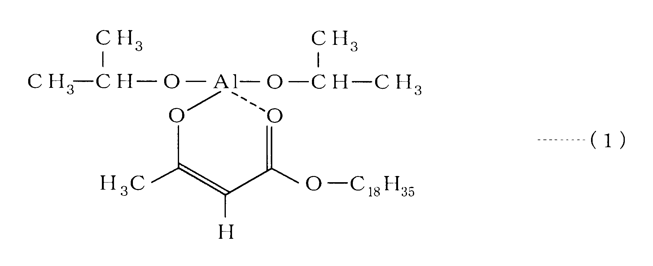



先ず硝酸銀を脱イオン水等の水に溶解して金属塩水溶液を調製する。一方、クエン酸ナトリウムを脱イオン水等の水に溶解させて得られた濃度10~40%のクエン酸ナトリウム水溶液に、窒素ガス等の不活性ガスの気流中で粒状又は粉状の硫酸第一鉄を直接加えて溶解させ、クエン酸イオンと第一鉄イオンを3:2のモル比で含有する還元剤水溶液を調製する。次に上記不活性ガス気流中で上記還元剤水溶液を撹拌しながら、この還元剤水溶液に上記金属塩水溶液を滴下して混合する。ここで、金属塩水溶液の添加量は還元剤水溶液の量の1/10以下になるように、各溶液の濃度を調整することで、室温の金属塩水溶液を滴下しても反応温度が30~60℃に保持されるようにすることが好ましい。また上記両水溶液の混合比は、還元剤として加えられる第1鉄イオンの当量が、金属イオンの当量の3倍となるように調整する。即ち、(金属塩水溶液中の金属イオンのモル数)×(金属イオンの価数)=3×(還元剤水溶液中の第1鉄イオンのモル数)となるように調整する。金属塩水溶液の滴下が終了した後、混合液の撹拌を更に10~300分間続けて金属コロイドからなる分散液を調製する。この分散液を室温で放置し、沈降した金属ナノ粒子の凝集物をデカンテーションや遠心分離法等により分離した後、この分離物に脱イオン水等の水を加えて分散体とし、限外ろ過により脱塩処理する。更に引き続いてアルコール類で置換洗浄して、金属(銀)の含有量を2.5~50質量%にする。その後、遠心分離機を用いこの遠心分離機の遠心力を調整して粗粒子を分離することにより、銀ナノ粒子が一次粒径10~50nmの範囲内の銀ナノ粒子を数平均で70%以上含有するように調製する。即ち、数平均で全ての銀ナノ粒子100%に対する一次粒径10~50nmの範囲内の銀ナノ粒子の占める割合が70%以上になるように調整する。これにより銀ナノ粒子を化学修飾する保護剤の有機分子主鎖の炭素骨格の炭素数が3である分散体が得られる。
還元剤水溶液を調製するときに用いたクエン酸ナトリウムをりんご酸ナトリウムに替えること以外は上記(a)と同様にして分散体を調製する。これにより銀ナノ粒子を化学修飾する有機分子主鎖の炭素骨格の炭素数が2である分散体が得られる。
還元剤水溶液を調製するときに用いたクエン酸ナトリウムをグリコール酸ナトリウムに替えること以外は上記(a)と同様にして分散体を調製する。これにより銀ナノ粒子を化学修飾する有機分子主鎖の炭素骨格の炭素数が1である分散体が得られる。
銀ナノ粒子以外の金属ナノ粒子を構成する金属としては、金、白金、パラジウム、ルテニウム、ニッケル、銅、錫、インジウム、亜鉛、鉄、クロム及びマンガンが挙げられる。金属塩水溶液を調製するときに用いた硝酸銀を、塩化金酸、塩化白金酸、硝酸パラジウム、三塩化ルテニウム、塩化ニッケル、硝酸第一銅、二塩化錫、硝酸インジウム、塩化亜鉛、硫酸鉄、硫酸クロム又は硫酸マンガンに替えること以外は上記(a)と同様にして分散体を調製する。これにより銀ナノ粒子以外の金属ナノ粒子を化学修飾する保護剤の有機分子主鎖の炭素骨格の炭素数が3である分散体が得られる。
本発明の第2の実施の形態を図4~図6に基づいて説明する。図4~図6において、図1~図3と同一符号は同一構成要素を示す。図4及び図5に示すように、薄膜シリコン太陽電池モジュール10は、絶縁性表面を有する基板11と、この基板11上に積層された光起電力素子15とを備える。光起電力素子15は、基板11上に、表面電極層12、光電変換ユニット13、透明導電膜14及び裏面電極層16の順に積層して形成される。そして、この光起電力素子15上に積層された補強膜用組成物を湿式塗工法により塗布して得られた層に紫外線照射するか又は加熱するか或いは紫外線照射した後に加熱して形成された裏面電極補強膜17とを備え、そして、この補強膜17上にバリア膜用組成物を湿式塗工法により塗布して得られた層に紫外線照射するか又は加熱するか或いは紫外線照射した後に加熱して形成されたバリア膜24を設けた構造を持つ。この実施の形態では、基板11の光入射側と反対の裏面側に、光起電力素子15と裏面電極補強膜17とバリア膜24とがこの順に配置される。なお、この第2の実施の形態では、基板11、表面電極層12、光電変換ユニット13、透明導電膜14、裏面電極層16及び裏面電極補強膜17については、上記第1の実施の形態と同様の構成であるので省略する。
本発明の第3の実施の形態を図7~図9に基づいて説明する。図7~図9において、図1~図3と同一符号は同一構成要素を示す。図7及び図8に示すように、薄膜シリコン太陽電池モジュール10は、絶縁性表面を有する基板11と、この基板11上に積層された光起電力素子15とを備える。光起電力素子15は、基板11上に、表面電極層12、光電変換ユニット13、透明導電膜14及び裏面電極層16の順に積層して形成される。そして、この光起電力素子15の裏面電極層16上にバリア膜用組成物を湿式塗工法により塗布して得られた層に紫外線照射するか又は加熱するか或いは紫外線照射した後に加熱して形成されたバリア膜24を設けた構造を持つ。この実施の形態では、基板11の光入射側と反対の裏面側に、光起電力素子15とバリア膜24とがこの順に配置される。なお、この第3の実施の形態では、基板11、表面電極層12、光電変換ユニット13、透明導電膜14及び裏面電極層16については、上記第1の実施の形態と同様の構成であり、バリア膜24については、上記第2の実施の形態と同様の構成であるので省略する。また、図4及び図5に示すように、この光起電力素子15上に積層された裏面電極補強膜17とを備え、そして、この補強膜17上にバリア膜用組成物を湿式塗工法により塗布して得られた層に紫外線照射するか又は加熱するか或いは紫外線照射した後に加熱して形成されたバリア膜24を設けた構造としてもよい。この場合の裏面電極補強膜17は、上記第2の実施の形態における湿式塗工法以外の、例えば、スパッタ法等によって形成される。減圧雰囲気で約150℃の温度で形成された防食効果の高いTi含有のスパッタ膜が好適である。スパッタ法による場合の裏面電極補強膜17の厚さは0.01~2.0μmの範囲内で形成するのが好ましい。この実施の形態では、基板11の光入射側と反対の裏面側に、光起電力素子15と裏面電極補強膜17とバリア膜24とがこの順に配置される。
先ず、以下の実施例58~80及び実施例104~126で形成する裏面電極層を構成する電極用組成物及びこの組成物を用いた裏面電極層の形成方法を表した、裏面電極層No.1~No.17を次の表1に示す。

先ず1,6-ヘキサンジオールジアクリレートとトリメチロールプロパントリアクリレートとを質量比1:1の割合で混合してモノマーを調製した。この混合モノマーと溶剤MIBK(メチルイソブチルケトン)とを質量比3:7の割合で混合した。次にこのアクリル系混合モノマーに光重合開始剤として1-ヒドロキシ-シクロヘキシル-フェニル-ケトンをアクリル系混合モノマー100質量%に対して5質量%分を添加し、均一になるまで攪拌した。なお、均一にならなかった場合には40℃程度まで加温して攪拌した。このベース液は紫外線(UV)の照射により硬化する。
先ずネオペンチルグリコールジアクリレートとテトラメチロールメタンテトラアクリレートとを質量比1:1の割合で混合モノマーを調製した。この混合モノマーと溶剤PGME(1-メトキシ-2-プロパノール)とを質量比1:1の割合で混合した。次にこのアクリル系混合モノマーに光重合開始剤として2-ヒドロキシ-2-メチル-1-フェニル-プロパン-1-オンをアクリル系混合モノマー100質量%に対して4質量%分を添加し、均一になるまで撹拌した。なお、均一にならなかった場合には40℃程度まで加温して攪拌した。このベース液は紫外線(UV)の照射により硬化する。
先ず1,6-ヘキサンジオールジアクリレートとジトリメチロールプロパンテトラアクリレートとを質量比4:6で混合モノマーを調製した。この混合モノマーと溶剤PGMEA(プロピレングリコールモノメチルエーテルアセテート)とを質量比4:6の割合で混合した。次にこのアクリル系混合モノマーに光重合開始剤として1-ヒドロキシ-シクロヘキシル-フェニル-ケトンをアクリル系混合モノマー100質量%に対して5質量%分を添加し、均一になるまで攪拌した。なお、均一にならなかった場合には40℃程度まで加温して攪拌した。このベース液は紫外線(UV)の照射により硬化する。
先ず溶剤BCA(ブチルカルビトールアセテート)とビフェニル型エポキシ樹脂(ジャパンエポキシレジン社製:YX4000)とを質量比7:3の割合で混合した。ここで、均一にならなかった場合には40℃程度まで加温して攪拌した。次にこの混合物に熱硬化剤として2-エチル-4-メチルイミダゾールを適量加えた。なお、このベース液は加熱により硬化する。
先ず溶剤ECA(エチルカルビトールアセテート)とクレゾールノボラック型エポキシ樹脂(DIC社製:EPICLON-665-EXP-S)とを質量比8:2の割合で混合した。ここで、均一にならなかった場合には40℃程度まで加温して攪拌した。次にこの混合物に熱硬化剤としてフッ化ホウ素・モノエタノールアミンを適量加えた。なお、このベース液は加熱により硬化する。
先ず溶剤BC(ブチルカルビトール)とビフェニル型エポキシ樹脂(日本化薬社製:NC3000)を質量比8:2の割合で混合した。ここで、均一にならなかった場合には40℃程度まで加温して攪拌した。次にこの混合物に対して熱硬化剤としてDICY(ジシアンジアミド)を適量加えた。なお、このベース液は加熱により硬化する。
先ず溶剤IPA(イソプロピルアルコール)と水とを質量比1:1の割合で混合して溶媒を調製した。次にこの混合溶媒94質量%に、水溶性セルロース誘導体であるヒドロキシプロピルセルロース1質量%と、ゼラチン5質量%と添加した後に、30℃に加温して混合した。なお、このベース液は加熱により硬化する。
先ず導電性酸化物微粒子として平均粒径0.025μmのATO(酸化アンチモン-酸化錫系複合酸化物)粒子(添加剤2)を6質量%と、カップリング剤としてジアルキルパイロホスファイト基を有するチタンカップリング剤(添加剤1)を9質量%と、分散媒としてエタノール及びブタノールの混合液(質量比98:2)を85質量%とを混合し、室温にて800rpmの回転速度で1時間攪拌した。次にこの混合物60gを100ccのガラス瓶中に入れ、直径0.3mmのジルコニアビーズ(昭和シェル石油社製:ミクロハイカ)100gを用いてペイントシェーカーで6時間分散することにより、ATO粒子の分散液を調製した。なお、ジアルキルパイロホスファイト基を有するチタンカップリング剤(添加剤1)は上記実施の形態に挙げた式(3)で表される。また、バインダとしてSiO2結合剤10質量%と、分散媒として上記エタノール及びブタノールの混合液(質量比98:2)90質量%とを混合してSiO2結合剤の分散液を調整した。なお、上記SiO2結合剤は次のようにして製造した。先ず攪拌しながら1.0gの12N-HClを25gの純水に溶解した。次に500mlのガラス製4つ口フラスコにテトラエトキシシラン140gとエチルアルコール240gとを入れ、上記HCl水溶液を一度に加えた後に、80℃に6時間保持して反応させて、SiO2結合剤を製造した。そしてATO粒子の分散液とSiO2結合剤の分散液とを混合してベース液を得た。このベース液は加熱により硬化する。
先ず導電性酸化物微粒子として平均粒径0.025μmのITO(酸化インジウム-酸化錫系複合酸化物)粒子(添加剤2)を8質量%と、カップリング剤としてジアルキルパイロホスファイト基を有するチタンカップリング剤(添加剤1)を2質量%と、分散媒としてエタノール及びブタノールの混合液(質量比98:2)を90質量%とを混合し、室温にて800rpmの回転速度で1時間攪拌した。次にこの混合物60gを100ccのガラス瓶中に入れ、直径0.3mmのジルコニアビーズ(昭和シェル石油社製:ミクロハイカ)100gを用いてペイントシェーカーで6時間分散した。これにより、ITO(酸化インジウム-酸化錫系複合酸化物)粒子の分散液を調製した。ここで、ジアルキルパイロホスファイト基を有するチタンカップリング剤(添加剤1)は上記実施の形態に挙げた式(2)で表される。また、SiO2結合剤の分散液を分類8のSiO2結合剤の分散液と同様にして調製した。そしてITO粒子の分散液とSiO2結合剤の分散液とを混合してベース液を得た。このベース液は加熱により硬化する。
先ず導電性酸化物微粒子として平均粒径0.025μmのAZO(酸化アルミニウム-酸化亜鉛系複合酸化物)粒子(添加剤2)を10質量%と、カップリング剤としてジアルキルパイロホスファイト基を有するチタンカップリング剤(添加剤1)を1.6質量%と、分散媒としてメタノール及びエタノールの混合液(質量比4:1)を90質量%とを混合し、室温にて800rpmの回転速度で1時間攪拌した。次にこの混合物60gを100ccのガラス瓶中に入れ、直径0.3mmのジルコニアビーズ(昭和シェル石油社製:ミクロハイカ)100gを用いてペイントシェーカーで6時間分散することにより、AZO粒子の分散液を調製した。ここで、ジアルキルパイロホスファイト基を有するチタンカップリング剤(添加剤1)は上記実施の形態に挙げた式(4)で表される。また、SiO2結合剤の分散液を分類8のSiO2結合剤の分散液と同様にして調製した。そしてAZO粒子の分散液とSiO2結合剤の分散液とを混合してベース液を得た。このベース液は加熱により硬化する。
先ず溶剤IPA(イソプロピルアルコール)とメタノールとを質量比4:1の割合で混合して溶媒を調製した。次いで、分類8と同様にして調製したSiO2結合剤を10質量%の割合で、上記調製した溶媒に混合してベース液を得た。このベース液は加熱により硬化する。
先ず1,6-ヘキサンジオールジアクリレートとトリメチロールプロパントリアクリレートとを質量比1:1の割合で混合してモノマーを調製した。次に、ペルヒドロポリシラザン10質量%をキシレン90質量%とを混合し、ペルヒドロポリシラザン系混合液を調製した。次いで、上記調製した混合モノマーとペルヒドロポリシラザン系混合液とを質量比3:97の割合で混合してベース液を得た。このベース液は加熱により硬化する。
先ずIPA(イソプロピルアルコール)85質量%に平均粒径20nm程度のコロイダルシリカを15質量%混合して添加剤1となるコロイダルシリカ分散液を調製した。次いで分類1のアクリル系ベース液と上記コロイダルシリカ分散液とを混合し、攪拌羽根付きディスパーで500rpm程度の回転速度で5分間攪拌して補強膜用組成物である塗液を調製した。次にこの塗液(補強膜用組成物)をスプレーコーティング装置により、基板上に表面電極層、光電変換ユニット、透明導電膜及び裏面電極層(銀電極層)がこの順に積層された積層体の裏面電極層(銀電極層)上に塗布して、硬化後の膜厚が500nmになるように補強膜用塗布層を形成した。更に真空乾燥により補強膜用塗布層から溶媒を脱離させた後に、紫外線照射装置により補強膜用塗布層に紫外線(UV)を照射して補強膜用塗布層をUV光硬化させ、裏面電極補強膜を得た。
先ず分類1のアクリル系ベース液85質量%と、添加剤1として平均直径5μmかつ平均厚さ20nm程度のマイカ粒子(コープケミカル社製:ミクロマイカ)15質量%とを混合し、回転子により室温にて300rpm程度の回転速度で1時間攪拌して混合物を全体になじませた。次いで5000rpm程度まで高速回転可能なディスパー羽根を用いて上記混合物を攪拌し、マイカ粒子をベース液中に分散させて補強膜用組成物である塗液を調製した。次にこの塗液(補強膜用組成物)をスプレーコーティング装置により、基板上に表面電極層、光電変換ユニット、透明導電膜及び裏面電極層(銀電極層)がこの順に積層された積層体の裏面電極層(銀電極層)上に塗布して、硬化後の膜厚が200nmになるように補強膜用塗布層を形成した。更に真空乾燥により補強膜用塗布層から溶媒を脱離させた後に、紫外線照射装置により補強膜用塗布層に紫外線(UV)を照射して補強膜用塗布層をUV光硬化させ、裏面電極補強膜を得た。
先ず分類2のアクリル系ベース液95質量%と、添加剤1として平均直径35μmかつ平均厚さ100nm程度の扁平なAl粒子(東洋アルミニウム社製:アルペースト)5質量%とを混合し、回転子により室温にて300rpm程度の回転速度で1時間攪拌して混合物を全体になじませた。次いで2000rpm程度まで高速回転可能なディスパー羽根を用いて上記混合物を攪拌し、Al粒子をベース液中に分散させて補強膜用組成物である塗液を調製した。次にこの塗液(補強膜用組成物)をスピンコーティング装置により、基板上に表面電極層、光電変換ユニット、透明導電膜及び裏面電極層(銀電極層)がこの順に積層された積層体の裏面電極層(銀電極層)上に塗布して、硬化後の膜厚が400nmになるように補強膜用塗布層を形成した。更に真空乾燥により補強膜用塗布層から溶媒を脱離させた後に、紫外線照射装置により補強膜用塗布層に紫外線(UV)を照射して補強膜用塗布層をUV光硬化させ、裏面電極補強膜を得た。
先ず分類2のアクリル系ベース液90質量%と、添加剤1として平均粒径20nm程度のシリカ粒子(扶桑化学工業社製:シリカ)10質量%とを混合し、回転子により室温にて300rpm程度の回転速度で1時間攪拌して混合物を全体になじませた。次いで5000rpm程度まで高速回転可能なディスパー羽根を用いて上記混合物を攪拌し、シリカ粒子をベース液中に分散させて補強膜用組成物である塗液を調製した。次にこの塗液(補強膜用組成物)をスピンコーティング装置により、基板上に表面電極層、光電変換ユニット、透明導電膜及び裏面電極層(銀電極層)がこの順に積層された積層体の裏面電極層(銀電極層)上に塗布して、硬化後の膜厚が300nmになるように補強膜用塗布層を形成した。更に真空乾燥により補強膜用塗布層から溶媒を脱離させた後に、紫外線照射装置により補強膜用塗布層に紫外線(UV)を照射して補強膜用塗布層をUV光硬化させ、裏面電極補強膜を得た。
先ず分類3のアクリル系ベース液95質量%と、添加剤1として平均直径140nmかつ平均厚さ50nm程度の扁平なスメクタイト粒子(コープケミカル社製:合成スメクタイト)5質量%とを混合し、回転子により室温にて300rpm程度の回転速度で1時間攪拌して混合物を全体になじませた。次いで5000rpm程度まで高速回転可能なディスパー羽根を用いて上記混合物を攪拌し、スメクタイト粒子をベース液中に分散させて補強膜用組成物である塗液を調製した。次にこの塗液(補強膜用組成物)をスピンコーティング装置により、基板上に表面電極層、光電変換ユニット、透明導電膜及び裏面電極層(銀電極層)がこの順に積層された積層体の裏面電極層(銀電極層)上に塗布して、硬化後の膜厚が150nmになるように補強膜用塗布層を形成した。更に真空乾燥により補強膜用塗布層から溶媒を脱離させた後に、紫外線照射装置により補強膜用塗布層に紫外線(UV)を照射して補強膜用塗布層をUV光硬化させ、裏面電極補強膜を得た。
先ず分類4のエポキシ系ベース液93質量%と、添加剤1として平均直径27μmかつ平均厚さ100nm程度の扁平なAl粒子(東洋アルミニウム社製:アルペースト)7質量%とを混合し、回転子により室温にて300rpm程度の回転速度で1時間攪拌して混合物を全体になじませた。次いで2000rpmまで高速回転可能なディスパー羽根を用いて上記混合物を攪拌し、Al粒子をベース液中に分散させて補強膜用組成物である塗液を調製した。次にこの塗液(補強膜用組成物)をスプレーコーティング装置により、基板上に表面電極層、光電変換ユニット、透明導電膜及び裏面電極層(銀電極層)がこの順に積層された積層体の裏面電極層(銀電極層)上に塗布して、硬化後の膜厚が400nmになるように補強膜用塗布層を形成した。更に室温で20分以上乾燥した後に、太陽電池モジュールを熱風乾燥炉内で150℃に20分間保持して補強膜用塗布層を熱硬化させ、裏面電極補強膜を得た。
先ず分類4のエポキシ系ベース液80質量%と、添加剤1として平均直径1μmかつ平均厚さ20nm程度のマイカ粒子(コープケミカル社製:ミクロマイカ)20質量%とを混合し、回転子により室温にて300rpm程度の回転速度で1時間攪拌して混合物を全体になじませた。次いで5000rpm程度まで高速回転可能なディスパー羽根を用いて上記混合物を攪拌し、マイカ粒子をベース液中に分散させて補強膜用組成物である塗液を調製した。このとき塗液が70℃以上にならないように注意して羽根形状と回転速度を調整した。次にこの塗液(補強膜用組成物)をスピンコーティング装置により、基板上に表面電極層、光電変換ユニット、透明導電膜及び裏面電極層(銀電極層)がこの順に積層された積層体の裏面電極層(銀電極層)上に塗布して、硬化後の膜厚が200nmになるように補強膜用塗布層を形成した。更に室温で20分以上乾燥した後に、太陽電池モジュールを熱風乾燥炉内で200℃に20分間保持して補強膜用塗布層を熱硬化させ、裏面電極補強膜を得た。
先ず分類5のエポキシ系ベース液97質量%と、添加剤1としてフュームドシリカ分散液(日本アエロジル社製:アエロジル)3質量%とを混合し、超音波振動器により室温で10分間分散混合して混合物を全体になじませ、補強膜用組成物である塗液を調製した。次にこの塗液(補強膜用組成物)をダイコーティング装置により、基板上に表面電極層、光電変換ユニット、透明導電膜及び裏面電極層(銀電極層)がこの順に積層された積層体の裏面電極層(銀電極層)上に塗布して、硬化後の膜厚が150nmになるように補強膜用塗布層を形成した。更に室温で20分以上乾燥した後に、太陽電池モジュールを熱風乾燥炉内で180℃に30分間保持して補強膜用塗布層を熱硬化させ、裏面電極補強膜を得た。なお、上記フュームドシリカ分散液は次のように調製した。先ずフュームドシリカ粒子10質量%と、IPA(イソプロピルアルコール)及びエタノールの混合溶媒(質量比2:1)90質量%とを混合した後に、室温にて800rpmの回転速度で1時間攪拌して混合物を調製した。次にこの混合物60gを100ccのガラス瓶中に入れ、直径0.3mmのジルコニアビーズ(昭和シェル石油社製:ミクロハイカ)100gを用いてペイントシェーカーで6時間分散することにより、導電性酸化物微粒子であるフュームドシリカ粒子の分散液を調製した。
先ず分類6のエポキシ系ベース液95質量%と、添加剤1として平均直径180nmかつ平均厚さ30nm程度の扁平なスメクタイト粒子(コープケミカル社製:合成スメクタイト)5質量%とを混合し、回転子により室温にて300rpm程度の回転速度で1時間攪拌して混合物を全体になじませた。次いで2000rpm程度まで高速回転可能なディスパー羽根を用いて攪拌し、スメクタイト粒子をベース液中に分散させて補強膜用組成物である塗液を調製した。このとき塗液が70℃以上にならないように注意して羽根形状と回転数を調整した。次にこの塗液(補強膜用組成物)をスリットコーティング装置により、基板上に表面電極層、光電変換ユニット、透明導電膜及び裏面電極層(銀電極層)がこの順に積層された積層体の裏面電極層(銀電極層)上に塗布して、硬化後の膜厚が400nmになるように補強膜用塗布層を形成した。更に室温で20分以上乾燥した後に、太陽電池モジュールを熱風乾燥炉内で200℃に20分間保持して補強膜用塗布層を熱硬化させ、裏面電極補強膜を得た。
先ず分類6のエポキシ系ベース液87質量%と、添加剤1としてコロイダルシリカ分散液13質量%とを混合し、遊星攪拌装置により室温で10分間混合して混合物を全体になじませ、補強膜用組成物である塗液を調製した。次にこの塗液(補強膜用組成物)をスクリーン印刷装置により、基板上に表面電極層、光電変換ユニット、透明導電膜及び裏面電極層(銀電極層)がこの順に積層された積層体の裏面電極層(銀電極層)上に塗布して、硬化後の膜厚が900nmになるように補強膜用塗布層を形成した。更に室温で20分以上乾燥した後に、太陽電池モジュールを熱風乾燥炉内で200℃に30分間保持して補強膜用塗布層を熱硬化させ、裏面電極補強膜を得た。なお、上記コロイダルシリカ分散液は補強膜No.8のフュームドシリカ分散液と同様にして調製した。
先ず分類7のセルロース系ベース液90質量%と、添加剤1として平均粒径30nm程度のシリカ粒子(扶桑化学工業社製:シリカ)10質量%とを混合し、回転子により室温にて300rpm程度の回転速度で1時間攪拌して混合物を全体になじませた。次いで5000rpm程度まで高速回転可能なディスパー羽根を用いて上記混合物を攪拌し、シリカ粒子をベース液中に分散させて補強膜用組成物である塗液を調製した。次にこの塗液(補強膜用組成物)をスピンコーティング装置により、基板上に表面電極層、光電変換ユニット、透明導電膜及び裏面電極層(銀電極層)がこの順に積層された積層体の裏面電極層(銀電極層)上に塗布して、硬化後の膜厚が400nmになるように補強膜用塗布層を形成した。更に室温で20分以上乾燥した後に、太陽電池モジュールを熱風乾燥炉内で180℃に20分間保持して補強膜用塗布層を熱硬化させ、裏面電極補強膜を得た。
先ずIPA(イソプロピルアルコール)85質量%に平均粒径20nm程度のコロイダルシリカを15質量%混合して添加剤3となるコロイダルシリカ分散液(日産化学社製:スノーテックス20)を調製した。次いで分類8のSiO2結合剤系ベース液75質量%と上記コロイダルシリカ分散液25質量%とを混合し、超音波振動器により室温で10分間分散混合して混合物を全体になじませ、補強膜用組成物である塗液を調製した。次にこの塗液(補強膜用組成物)をスピンコーティング装置により、基板上に表面電極層、光電変換ユニット、透明導電膜及び裏面電極層(銀電極層)がこの順に積層された積層体の裏面電極層(銀電極層)上に塗布して、硬化後の膜厚が200nmになるように補強膜用塗布層を形成した。更に真空乾燥により補強膜用塗布層から溶媒を離脱させた後に、太陽電池モジュールを熱風乾燥炉内で200℃に30分間保持して補強膜用塗布層を熱硬化させ、裏面電極補強膜を得た。なお、表2において、添加剤1のチタンカップリング剤1と添加剤2のATO(酸化アンチモン-酸化錫系複合酸化物)粒子はベース液中に既に含まれているため、これらの添加量は塗液(補強膜用組成物)全体を100質量%としたときの割合(カッコ付きの数値)で示した。
先ず分類8のSiO2結合剤系ベース液98質量%と、添加剤3としてフュームドシリカ分散液2質量%とを混合し、超音波振動器により室温にて10分間分散混合して混合物を全体になじませ、補強膜用組成物である塗液を調製した。次にこの塗液(補強膜用組成物)をスプレーコーティング装置により、基板上に表面電極層、光電変換ユニット、透明導電膜及び裏面電極層(銀電極層)がこの順に積層された積層体の裏面電極層(銀電極層)上に塗布して、硬化後の膜厚が150nmになるように補強膜用塗布層を形成した。更に真空乾燥により補強膜用塗布層から溶媒を離脱させた後に、太陽電池モジュールを熱風乾燥炉内で150℃に20分間保持して補強膜用塗布層を熱硬化させ、裏面電極補強膜を得た。なお、表2において、添加剤1のチタンカップリング剤1と添加剤2のATO(酸化アンチモン-酸化錫系複合酸化物)粒子はベース液中に既に含まれているため、これらの添加量は塗液(補強膜用組成物)全体を100質量%としたときの割合(カッコ付きの数値)で示した。また上記フュームドシリカ分散液は補強膜No.8のフュームドシリカ分散液と同様にして調製した。
先ず分類9のSiO2結合剤系ベース液95質量%と、添加剤3としてフュームドシリカ分散液5質量%とを混合し、超音波振動器により室温にて10分間分散混合して混合物を全体になじませ、補強膜用組成物である塗液を調製した。次にこの塗液(補強膜用組成物)をダイコーティング装置により、基板上に表面電極層、光電変換ユニット、透明導電膜及び裏面電極層(銀電極層)がこの順に積層された積層体の裏面電極層(銀電極層)上に塗布して、硬化後の膜厚が350nmになるように補強膜用塗布層を形成した。更に真空乾燥により補強膜用塗布層から溶媒を離脱させた後に、太陽電池モジュールを熱風乾燥炉内で180℃に20分間保持して補強膜用塗布層を熱硬化させ、裏面電極補強膜を得た。なお、表2において、添加剤1のチタンカップリング剤2と添加剤2のITO(酸化インジウム-酸化錫系複合酸化物)粒子はベース液中に既に含まれているため、これらの添加量は塗液(補強膜用組成物)全体を100質量%としたときの割合(カッコ付きの数値)で示した。また上記フュームドシリカ分散液は補強膜No.8のフュームドシリカ分散液と同様にして調製した。
先ず分類9のSiO2結合剤系ベース液90質量%と、添加剤3として平均直径5μmかつ平均厚さ20nm程度のマイカ粒子(コープケミカル社製:ミクロマイカ)10質量%とを混合し、回転子により室温にて300rpm程度の回転速度で1時間攪拌して混合物を全体になじませた。次いで5000rpm程度まで高速回転可能なディスパー羽根を用いて上記混合物を攪拌し、マイカ粒子をベース液中に分散させて補強膜用組成物である塗液を調製した。このとき塗液が70℃以上にならないように注意して羽根形状と回転速度を調整した。次にこの塗液(補強膜用組成物)をスピンコーティング装置により、基板上に表面電極層、光電変換ユニット、透明導電膜及び裏面電極層(銀電極層)がこの順に積層された積層体の裏面電極層(銀電極層)上に塗布して、硬化後の膜厚が200nmになるように補強膜用塗布層を形成した。更に室温で20分以上乾燥した後に、太陽電池モジュールを熱風乾燥炉内で200℃に30分間保持して補強膜用塗布層を熱硬化させ、裏面電極補強膜を得た。なお、表2において、添加剤1のチタンカップリング剤2と添加剤2のITO(酸化インジウム-酸化錫系複合酸化物)粒子はベース液中に既に含まれているため、これらの添加量は塗液(補強膜用組成物)全体を100質量%としたときの割合(カッコ付きの数値)で示した。
先ず分類1のアクリル系ベース液96質量%と、添加剤1として平均直径27μmかつ平均厚さ100nm程度のAl粒子(東洋アルミニウム社製:アルペースト)4質量%とを混合し、回転子により室温にて300rpm程度の回転速度で1時間攪拌して混合物を全体になじませた。次いで2000rpm程度まで高速回転可能なディスパー羽根を用いて上記混合物を攪拌し、Al粒子をベース液中に分散させて補強膜用組成物である塗液を調製した。次にこの塗液(補強膜用組成物)をダイコーティング装置により、基板上に表面電極層、光電変換ユニット、透明導電膜及び裏面電極層(銀電極層)がこの順に積層された積層体の裏面電極層(銀電極層)上に塗布して、硬化後の膜厚が250nmになるように補強膜用塗布層を形成した。更に真空乾燥により補強膜用塗布層から溶媒を脱離させ、紫外線照射装置により補強膜用塗布層に紫外線(UV)を照射して補強膜用塗布層をUV光硬化させた後に、太陽電池モジュールを熱風乾燥炉内で70℃に3時間保持して熱硬化させることにより、十分に硬化した裏面電極補強膜を得た。
先ずIPA(イソプロピルアルコール)85質量%に平均粒径20nm程度のコロイダルシリカを15質量%混合して添加剤1となるコロイダルシリカ分散液(日産化学社製:IPA-ST-UP)を調製した。次いで分類1のアクリル系ベース液93質量%と上記コロイダルシリカ分散液7質量%とを混合し、超音波振動器により室温で10分間分散混合して混合物を全体になじませ、補強膜用組成物である塗液を調製した。次にこの塗液(補強膜用組成物)をスピンコーティング装置により、基板上に表面電極層、光電変換ユニット、透明導電膜及び裏面電極層(銀電極層)がこの順に積層された積層体の裏面電極層(銀電極層)上に塗布して、硬化後の膜厚が400nmになるように補強膜用塗布層を形成した。更に真空乾燥により補強膜用塗布層から溶媒を脱離させ、紫外線照射装置により補強膜用塗布層に紫外線(UV)を照射して補強膜用塗布層をUV光硬化させた後に、太陽電池モジュールを熱風乾燥炉内で70℃に3時間保持して熱硬化させることにより、十分に硬化した裏面電極補強膜を得た。

先ずIPA(イソプロピルアルコール)85質量%に平均粒径20nm程度のコロイダルシリカを15質量%混合して添加剤1となるコロイダルシリカ分散液を調製した。次いで分類1のアクリル系ベース液と上記コロイダルシリカ分散液とを混合し、攪拌羽根付きディスパーで500rpm程度の回転速度で5分間攪拌してバリア膜用組成物である塗液を調製した。次にこの塗液(バリア膜用組成物)をスプレーコーティング装置により、基板上に表面電極層、光電変換ユニット、透明導電膜、裏面電極層及び裏面電極補強膜がこの順に積層された積層体の補強膜上に塗布して、硬化後の膜厚が800nmになるように塗布層を形成した。更に真空乾燥により塗布層から溶媒を脱離させた後に、紫外線照射装置により塗布層に紫外線(UV)を照射して塗布層をUV光硬化させ、バリア膜を得た。
先ず分類1のアクリル系ベース液85質量%と、添加剤1として平均直径5μmかつ平均厚さ20nm程度のマイカ粒子(コープケミカル社製:ミクロマイカ)15質量%とを混合し、回転子により室温にて300rpm程度の回転速度で1時間攪拌して混合物を全体になじませた。次いで5000rpm程度まで高速回転可能なディスパー羽根を用いて上記混合物を攪拌し、マイカ粒子をベース液中に分散させてバリア膜用組成物である塗液を調製した。次にこの塗液(バリア膜用組成物)をスプレーコーティング装置により、基板上に表面電極層、光電変換ユニット、透明導電膜、裏面電極層及び裏面電極補強膜がこの順に積層された積層体の補強膜上に塗布して、硬化後の膜厚が600nmになるように塗布層を形成した。更に真空乾燥により塗布層から溶媒を脱離させた後に、紫外線照射装置により塗布層に紫外線(UV)を照射して塗布層をUV光硬化させ、バリア膜を得た。
先ず分類2のアクリル系ベース液95質量%と、添加剤1として平均直径35μmかつ平均厚さ100nm程度のAl粒子(東洋アルミニウム社製:アルペースト)5質量%とを混合し、回転子により室温にて300rpm程度の回転速度で1時間攪拌して混合物を全体になじませた。次いで2000rpm程度まで高速回転可能なディスパー羽根を用いて上記混合物を攪拌し、Al粒子をベース液中に分散させてバリア膜用組成物である塗液を調製した。次にこの塗液(バリア膜用組成物)をスピンコーティング装置により、基板上に表面電極層、光電変換ユニット、透明導電膜、裏面電極層及び裏面電極補強膜がこの順に積層された積層体の補強膜上に塗布して、硬化後の膜厚が400nmになるように塗布層を形成した。更に真空乾燥により塗布層から溶媒を脱離させた後に、紫外線照射装置により塗布層に紫外線(UV)を照射して塗布層をUV光硬化させ、バリア膜を得た。
先ず分類2のアクリル系ベース液90質量%と、添加剤1として平均粒径20nm程度のシリカ粒子(扶桑化学工業社製:シリカ)10質量%とを混合し、回転子により室温にて300rpm程度の回転速度で1時間攪拌して混合物を全体になじませた。次いで5000rpm程度まで高速回転可能なディスパー羽根を用いて上記混合物を攪拌し、シリカ粒子をベース液中に分散させてバリア膜用組成物である塗液を調製した。次にこの塗液(バリア膜用組成物)をスピンコーティング装置により、基板上に表面電極層、光電変換ユニット、透明導電膜、裏面電極層及び裏面電極補強膜がこの順に積層された積層体の補強膜上に塗布して、硬化後の膜厚が750nmになるように塗布層を形成した。更に真空乾燥により塗布層から溶媒を脱離させた後に、紫外線照射装置により塗布層に紫外線(UV)を照射して塗布層をUV光硬化させ、バリア膜を得た。
先ず分類3のアクリル系ベース液95質量%と、添加剤1として平均直径140nmかつ平均厚さ50nm程度のスメクタイト粒子(コープケミカル社製:合成スメクタイト)5質量%とを混合し、回転子により室温にて300rpm程度の回転速度で1時間攪拌して混合物を全体になじませた。次いで5000rpm程度まで高速回転可能なディスパー羽根を用いて上記混合物を攪拌し、スメクタイト粒子をベース液中に分散させてバリア膜用組成物である塗液を調製した。次にこの塗液(バリア膜用組成物)をスピンコーティング装置により、基板上に表面電極層、光電変換ユニット、透明導電膜、裏面電極層及び裏面電極補強膜がこの順に積層された積層体の補強膜上に塗布して、硬化後の膜厚が1000nmになるように塗布層を形成した。更に真空乾燥により塗布層から溶媒を脱離させた後に、紫外線照射装置により塗布層に紫外線(UV)を照射して塗布層をUV光硬化させ、バリア膜を得た。
先ず分類4のエポキシ系ベース液93質量%と、添加剤1として平均直径27μmかつ平均厚さ100nm程度のAl粒子(東洋アルミニウム社製:アルペースト)とを混合し、回転子により室温にて300rpm程度の回転速度で1時間攪拌して混合物を全体になじませた。次いで2000rpmまで高速回転可能なディスパー羽根を用いて上記混合物を攪拌し、Al粒子をベース液中に分散させてバリア膜用組成物である塗液を調製した。次にこの塗液(バリア膜用組成物)をスプレーコーティング装置により、基板上に表面電極層、光電変換ユニット、透明導電膜、裏面電極層及び裏面電極補強膜がこの順に積層された積層体の補強膜上に塗布して、硬化後の膜厚が1200nmになるように塗布層を形成した。更に室温で20分以上乾燥した後に、太陽電池モジュールを熱風乾燥炉内で150℃に20分間保持して塗布層を熱硬化させ、バリア膜を得た。
先ず分類4のエポキシ系ベース液80質量%と、添加剤1として平均直径1μmかつ平均厚さ20nm程度のマイカ粒子(コープケミカル社製:ミクロマイカ)20質量%とを混合し、回転子により室温にて300rpm程度の回転速度で1時間攪拌して混合物を全体になじませた。次いで5000rpm程度まで高速回転可能なディスパー羽根を用いて上記混合物を攪拌し、マイカ粒子をベース液中に分散させてバリア膜用組成物である塗液を調製した。このとき塗液が70℃以上にならないように注意して羽根形状と回転速度を調整した。次にこの塗液(バリア膜用組成物)をスピンコーティング装置により、基板上に表面電極層、光電変換ユニット、透明導電膜、裏面電極層及び裏面電極補強膜がこの順に積層された積層体の補強膜上に塗布して、硬化後の膜厚が900nmになるように塗布層を形成した。更に室温で20分以上乾燥した後に、太陽電池モジュールを熱風乾燥炉内で200℃に20分間保持して塗布層を熱硬化させ、バリア膜を得た。
先ず分類5のエポキシ系ベース液97質量%と、添加剤1としてフュームドシリカ分散液(日本アエロジル社製:アエロジル)3質量%とを混合し、超音波振動器により室温で10分間分散混合して混合物を全体になじませ、バリア膜用組成物である塗液を調製した。次にこの塗液(バリア膜用組成物)をダイコーティング装置により、基板上に表面電極層、光電変換ユニット、透明導電膜、裏面電極層及び裏面電極補強膜がこの順に積層された積層体の補強膜上に塗布して、硬化後の膜厚が150nmになるように塗布層を形成した。更に室温で20分以上乾燥した後に、太陽電池モジュールを熱風乾燥炉内で180℃に30分間保持して塗布層を熱硬化させ、バリア膜を得た。なお、上記フュームドシリカ分散液は次のように調製した。先ずフュームドシリカ粒子10質量%と、IPA(イソプロピルアルコール)及びエタノールの混合溶媒(質量比2:1)90質量%とを混合した後に、室温にて800rpmの回転速度で1時間攪拌して混合物を調製した。次にこの混合物60gを100ccのガラス瓶中に入れ、直径0.3mmのジルコニアビーズ(昭和シェル石油社製:ミクロハイカ)100gを用いてペイントシェーカーで6時間分散することにより、導電性酸化物微粒子であるフュームドシリカ粒子の分散液を調製した。
先ず分類6のエポキシ系ベース液95質量%と、添加剤1として平均直径180nmかつ平均厚さ30nm程度の扁平なスメクタイト粒子(コープケミカル社製:合成スメクタイト)5質量%とを混合し、回転子により室温にて300rpm程度の回転速度で1時間攪拌して混合物を全体になじませた。次いで2000rpm程度まで高速回転可能なディスパー羽根を用いて攪拌し、スメクタイト粒子をベース液中に分散させてバリア膜用組成物である塗液を調製した。このとき塗液が70℃以上にならないように注意して羽根形状と回転数を調整した。次にこの塗液(バリア膜用組成物)をスリットコーティング装置により、基板上に表面電極層、光電変換ユニット、透明導電膜、裏面電極層及び裏面電極補強膜がこの順に積層された積層体の補強膜上に塗布して、硬化後の膜厚が400nmになるように塗布層を形成した。更に室温で20分以上乾燥した後に、太陽電池モジュールを熱風乾燥炉内で200℃に20分間保持して塗布層を熱硬化させ、バリア膜を得た。
先ず分類6のエポキシ系ベース液87質量%と、添加剤1としてコロイダルシリカ分散液13質量%とを混合し、遊星攪拌装置により室温で10分間混合して混合物を全体になじませ、バリア膜用組成物である塗液を調製した。次にこの塗液(バリア膜用組成物)をスクリーン印刷装置により、基板上に表面電極層、光電変換ユニット、透明導電膜、裏面電極層及び裏面電極補強膜がこの順に積層された積層体の補強膜上に塗布して、硬化後の膜厚が900nmになるように塗布層を形成した。更に室温で20分以上乾燥した後に、太陽電池モジュールを熱風乾燥炉内で200℃に30分間保持して塗布層を熱硬化させ、バリア膜を得た。なお、上記コロイダルシリカ分散液はバリア膜No.8のフュームドシリカ分散液と同様にして調製した。
先ず分類7のセルロース系ベース液90質量%と、添加剤1として平均粒径30nm程度のシリカ粒子(扶桑化学工業社製:シリカ)10質量%とを混合し、回転子により室温にて300rpm程度の回転速度で1時間攪拌して混合物を全体になじませた。次いで5000rpm程度まで高速回転可能なディスパー羽根を用いて上記混合物を攪拌し、シリカ粒子をベース液中に分散させてバリア膜用組成物である塗液を調製した。次にこの塗液(バリア膜用組成物)をスピンコーティング装置により、基板上に表面電極層、光電変換ユニット、透明導電膜、裏面電極層及び裏面電極補強膜がこの順に積層された積層体の補強膜上に塗布して、硬化後の膜厚が700nmになるように塗布層を形成した。更に室温で20分以上乾燥した後に、太陽電池モジュールを熱風乾燥炉内で180℃に20分間保持して塗布層を熱硬化させ、バリア膜を得た。
先ずIPA(イソプロピルアルコール)85質量%に平均粒径20nm程度のコロイダルシリカを15質量%混合して添加剤3となるコロイダルシリカ分散液(日産化学社製:スノーテックス20)を調製した。次いで分類8のSiO2結合剤系ベース液75質量%と上記コロイダルシリカ分散液25質量%とを混合し、超音波振動器により室温で10分間分散混合して混合物を全体になじませ、バリア膜用組成物である塗液を調製した。次にこの塗液(バリア膜用組成物)をスピンコーティング装置により、基板上に表面電極層、光電変換ユニット、透明導電膜、裏面電極層及び裏面電極補強膜がこの順に積層された積層体の補強膜上に塗布して、硬化後の膜厚が200nmになるように塗布層を形成した。更に真空乾燥により塗布層から溶媒を離脱させた後に、太陽電池モジュールを熱風乾燥炉内で200℃に30分間保持して塗布層を熱硬化させ、バリア膜を得た。なお、表3において、添加剤1のチタンカップリング剤1と添加剤2のATO(アンチモンドープ酸化錫)粒子はベース液中に既に含まれているため、これらの添加量は塗液(バリア膜用組成物)全体を100質量%としたときの割合(カッコ付きの数値)で示した。
先ず分類8のSiO2結合剤系ベース液98質量%と、添加剤3としてフュームドシリカ分散液2質量%とを混合し、超音波振動器により室温にて10分間分散混合して混合物を全体になじませ、バリア膜用組成物である塗液を調製した。次にこの塗液(バリア膜用組成物)をスプレーコーティング装置により、基板上に表面電極層、光電変換ユニット、透明導電膜、裏面電極層及び裏面電極補強膜がこの順に積層された積層体の補強膜上に塗布して、硬化後の膜厚が150nmになるように塗布層を形成した。更に真空乾燥により塗布層から溶媒を離脱させた後に、太陽電池モジュールを熱風乾燥炉内で150℃に20分間保持して塗布層を熱硬化させ、バリア膜を得た。なお、表3において、添加剤1のチタンカップリング剤1と添加剤2のATO(アンチモンドープ酸化錫)粒子はベース液中に既に含まれているため、これらの添加量は塗液(バリア膜用組成物)全体を100質量%としたときの割合(カッコ付きの数値)で示した。また上記フュームドシリカ分散液はバリア膜No.8のフュームドシリカ分散液と同様にして調製した。
先ず分類9のSiO2結合剤系ベース液95質量%と、添加剤3としてフュームドシリカ分散液5質量%とを混合し、超音波振動器により室温にて10分間分散混合して混合物を全体になじませ、バリア膜用組成物である塗液を調製した。次にこの塗液(バリア膜用組成物)をダイコーティング装置により、基板上に表面電極層、光電変換ユニット、透明導電膜、裏面電極層及び裏面電極補強膜がこの順に積層された積層体の補強膜上に塗布して、硬化後の膜厚が350nmになるように塗布層を形成した。更に真空乾燥により塗布層から溶媒を離脱させた後に、太陽電池モジュールを熱風乾燥炉内で180℃に20分間保持して塗布層を熱硬化させ、バリア膜を得た。なお、表3において、添加剤1のチタンカップリング剤2と添加剤2のITO(インジウム錫酸化物)粒子はベース液中に既に含まれているため、これらの添加量は塗液(バリア膜用組成物)全体を100質量%としたときの割合(カッコ付きの数値)で示した。また上記フュームドシリカ分散液はバリア膜No.8のフュームドシリカ分散液と同様にして調製した。
先ず分類9のSiO2結合剤系ベース液90質量%と、添加剤3として平均直径5μmかつ平均厚さ20nm程度のマイカ粒子(コープケミカル社製:ミクロマイカ)10質量%とを混合し、回転子により室温にて300rpm程度の回転速度で1時間攪拌して混合物を全体になじませた。次いで5000rpm程度まで高速回転可能なディスパー羽根を用いて上記混合物を攪拌し、マイカ粒子をベース液中に分散させてバリア膜用組成物である塗液を調製した。このとき塗液が70℃以上にならないように注意して羽根形状と回転速度を調整した。次にこの塗液(バリア膜用組成物)をスピンコーティング装置により、基板上に表面電極層、光電変換ユニット、透明導電膜、裏面電極層及び裏面電極補強膜がこの順に積層された積層体の補強膜上に塗布して、硬化後の膜厚が200nmになるように塗布層を形成した。更に室温で20分以上乾燥した後に、太陽電池モジュールを熱風乾燥炉内で200℃に30分間保持して塗布層を熱硬化させ、バリア膜を得た。なお、表3において、添加剤1のチタンカップリング剤2と添加剤2のITO(インジウム錫酸化物)粒子はベース液中に既に含まれているため、これらの添加量は塗液(バリア膜用組成物)全体を100質量%としたときの割合(カッコ付きの数値)で示した。
先ず分類10のSiO2結合剤系ベース液30質量%と、添加剤3としてフュームドシリカ分散液70質量%とを混合し、超音波振動器により室温にて10分間分散混合して混合物を全体になじませ、バリア膜用組成物である塗液を調製した。次にこの塗液(バリア膜用組成物)をスピンコーティング装置により、基板上に表面電極層、光電変換ユニット、透明導電膜、裏面電極層及び裏面電極補強膜がこの順に積層された積層体の補強膜上に塗布して、硬化後の膜厚が300nmになるように塗布層を形成した。更に室温で20分以上乾燥した後に、太陽電池モジュールを熱風乾燥炉内で150℃に30分間保持して塗布層を熱硬化させ、バリア膜を得た。なお、表3において、添加剤1のチタンカップリング剤3と添加剤2のAZO(アンチモンドープ酸化錫)粒子はベース液中に既に含まれているため、これらの添加量は塗液(バリア膜用組成物)全体を100質量%としたときの割合(カッコ付きの数値)で示した。また上記フュームドシリカ分散液はバリア膜No.8のフュームドシリカ分散液と同様にして調製した。
先ず分類10のSiO2結合剤系ベース液50質量%とコロイダルシリカ分散液50質量%とを混合し、超音波振動器により室温で10分間分散混合して混合物を全体になじませ、バリア膜用組成物である塗液を調製した。次にこの塗液(バリア膜用組成物)をスプレーコーティング装置により、基板上に表面電極層、光電変換ユニット、透明導電膜、裏面電極層及び裏面電極補強膜がこの順に積層された積層体の補強膜上に塗布して、硬化後の膜厚が250nmになるように塗布層を形成した。更に室温で20分以上乾燥した後に、太陽電池モジュールを熱風乾燥炉内で150℃に30分間保持して塗布層を熱硬化させ、バリア膜を得た。なお、上記コロイダル分散液は次のように調製した。先ずコロイダルシリカ粒子10質量%と、メタノール変性アルコール及びIPA(イソプロピルアルコール)の混合溶媒(質量比 4:1)90質量%とを混合した後に、室温にて800rpmの回転速度で1時間攪拌して混合物を調製した。次にこの混合物60gを100ccのガラス瓶中に入れ、直径0.3mmのジルコニアビーズ(昭和シェル石油社製:ミクロハイカ)100gを用いてペイントシェーカーで6時間分散することにより、コロイダルシリカ分散液を調製した。また、表4において、添加剤1のチタンカップリング剤3と添加剤2のATO(アンチモンドープ酸化錫)粒子はベース液中に既に含まれているため、これらの添加量は塗液(バリア膜用組成物)全体を100質量%としたときの割合(カッコ付きの数値)で示した。
先ず分類11のSiO2結合剤系ベース液30質量%と、添加剤1としてフュームドシリカ分散液(日本アエロジル社製:アエロジル)70質量%とを混合し、超音波振動器により室温で10分間分散混合して混合物を全体になじませ、バリア膜用組成物である塗液を調製した。次にこの塗液(バリア膜用組成物)をスピンコーティング装置により、基板上に表面電極層、光電変換ユニット、透明導電膜、裏面電極層及び裏面電極補強膜がこの順に積層された積層体の補強膜上に塗布して、硬化後の膜厚が400nmになるように塗布層を形成した。更に室温で20分以上乾燥した後に、太陽電池モジュールを熱風乾燥炉内で200℃に30分間保持して塗布層を熱硬化させ、バリア膜を得た。なお、上記フュームドシリカ分散液はバリア膜No.8のフュームドシリカ分散液と同様にして調製した。
先ず分類11のSiO2結合剤系ベース液50質量%と、添加剤1として平均直径1μmかつ平均厚さ20nm程度のマイカ粒子(コープケミカル社製:ミクロマイカ)を含む分散液50質量%とを混合し、回転子により室温にて300rpm程度の回転速度で1時間攪拌して混合物を全体になじませた。次いで5000rpm程度まで高速回転可能なディスパー羽根を用いて上記混合物を攪拌し、バリア膜用組成物である塗液を調製した。次にこの塗液(バリア膜用組成物)をスピンコーティング装置により、基板上に表面電極層、光電変換ユニット、透明導電膜、裏面電極層及び裏面電極補強膜がこの順に積層された積層体の補強膜上に塗布して、硬化後の膜厚が600nmになるように塗布層を形成した。更に室温で20分以上乾燥した後に、太陽電池モジュールを熱風乾燥炉内で200℃に30分間保持して塗布層を熱硬化させ、バリア膜を得た。なお、上記マイカ分散液は次のように調製した。先ずマイカ粒子10質量%と、IPA(イソプロピルアルコール)及びエタノールの混合溶媒(質量比 2:1)80質量%とを混合した後に、室温にて300rpmの回転速度で1時間攪拌して材料を全体になじませた、更に5000rpm程度まで高速回転可能なディスパー羽根を用いて攪拌し調製した。
先ずIPA(イソプロピルアルコール)85質量%に平均粒径20nm程度のコロイダルシリカを15質量%混合して添加剤1となるコロイダルシリカ分散液(日産化学社製:IPA-ST)を調製した。次いで分類11のアクリル系ベース液40質量%と上記コロイダルシリカ分散液60質量%とを混合し、超音波振動器により室温で10分間分散混合して混合物を全体になじませ、バリア膜用組成物である塗液を調製した。次にこの塗液(バリア膜用組成物)をスプレーコーティング装置により、基板上に表面電極層、光電変換ユニット、透明導電膜、裏面電極層及び裏面電極補強膜がこの順に積層された積層体の補強膜上に塗布して、硬化後の膜厚が300nmになるように塗布層を形成した。更に室温で20分以上乾燥した後に、太陽電池モジュールを熱風乾燥炉内で180℃に30分間保持して塗布層を熱硬化させ、十分に硬化したバリア膜を得た。
先ず分類12のSiO2結合剤系ベース液90質量%と、添加剤1として平均直径5μmかつ平均厚さ20nm程度のマイカ粒子(コープケミカル社製:ミクロマイカ)10質量%とを混合し、回転子により室温にて300rpm程度の回転速度で1時間攪拌して混合物を全体になじませた。次いで5000rpm程度まで高速回転可能なディスパー羽根を用いて上記混合物を攪拌し、マイカ粒子をベース液中に分散させてバリア膜用組成物である塗液を調製した。次にこの塗液(バリア膜用組成物)をスピンコーティング装置により、基板上に表面電極層、光電変換ユニット、透明導電膜、裏面電極層及び裏面電極補強膜がこの順に積層された積層体の補強膜上に塗布して、硬化後の膜厚が400nmになるように塗布層を形成した。更に室温で20分以上乾燥した後に、太陽電池モジュールを熱風乾燥炉内で200℃に30分間保持して塗布層を熱硬化させ、バリア膜を得た。
先ず分類12のSiO2結合剤系ベース液95質量%と、添加剤1として平均直径35μmかつ平均厚さ100nm程度のAl粒子(東洋アルミニウム社製:アルペースト)5質量%とを混合し、回転子により室温にて300rpm程度の回転速度で1時間攪拌して混合物を全体になじませた。次いで2000rpm程度まで高速回転可能なディスパー羽根を用いて上記混合物を攪拌し、Al粒子をベース液中に分散させてバリア膜用組成物である塗液を調製した。次にこの塗液(バリア膜用組成物)をスプレーコーティング装置により、基板上に表面電極層、光電変換ユニット、透明導電膜、裏面電極層及び裏面電極補強膜がこの順に積層された積層体の補強膜上に塗布して、硬化後の膜厚が500nmになるように塗布層を形成した。更に室温で20分以上乾燥した後に、太陽電池モジュールを熱風乾燥炉内で200℃に30分間保持して塗布層を熱硬化させ、バリア膜を得た。
先ず分類1のアクリル系ベース液96質量%と、添加剤1として平均直径27μmかつ平均厚さ100nm程度のAl粒子(東洋アルミニウム社製:アルペースト)4質量%とを混合し、回転子により室温にて300rpm程度の回転速度で1時間攪拌して混合物を全体になじませた。次いで2000rpm程度まで高速回転可能なディスパー羽根を用いて上記混合物を攪拌し、Al粒子をベース液中に分散させてバリア膜用組成物である塗液を調製した。次にこの塗液(バリア膜用組成物)をダイコーティング装置により、基板上に表面電極層、光電変換ユニット、透明導電膜、裏面電極層及び裏面電極補強膜がこの順に積層された積層体の補強膜上に塗布して、硬化後の膜厚が1100nmになるように塗布層を形成した。更に真空乾燥により塗布層から溶媒を脱離させ、紫外線照射装置により塗布層に紫外線(UV)を照射して塗布層をUV光硬化させた後に、太陽電池モジュールを熱風乾燥炉内で70℃に3時間保持して熱硬化させることにより、十分に硬化したバリア膜を得た。
先ずIPA(イソプロピルアルコール)85質量%に平均粒径20nm程度のコロイダルシリカを15質量%混合して添加剤1となるコロイダルシリカ分散液(日産化学社製:IPA-ST-UP)を調製した。次いで分類1のアクリル系ベース液93質量%と上記コロイダルシリカ分散液7質量%とを混合し、超音波振動器により室温で10分間分散混合して混合物を全体になじませ、バリア膜用組成物である塗液を調製した。次にこの塗液(バリア膜用組成物)をスピンコーティング装置により、基板上に表面電極層、光電変換ユニット、透明導電膜、裏面電極層及び裏面電極補強膜がこの順に積層された積層体の補強膜上に塗布して、硬化後の膜厚が800nmになるように塗布層を形成した。更に真空乾燥により塗布層から溶媒を脱離させ、紫外線照射装置により塗布層に紫外線(UV)を照射して塗布層をUV光硬化させた後に、太陽電池モジュールを熱風乾燥炉内で70℃に3時間保持して熱硬化させることにより、十分に硬化したバリア膜を得た。
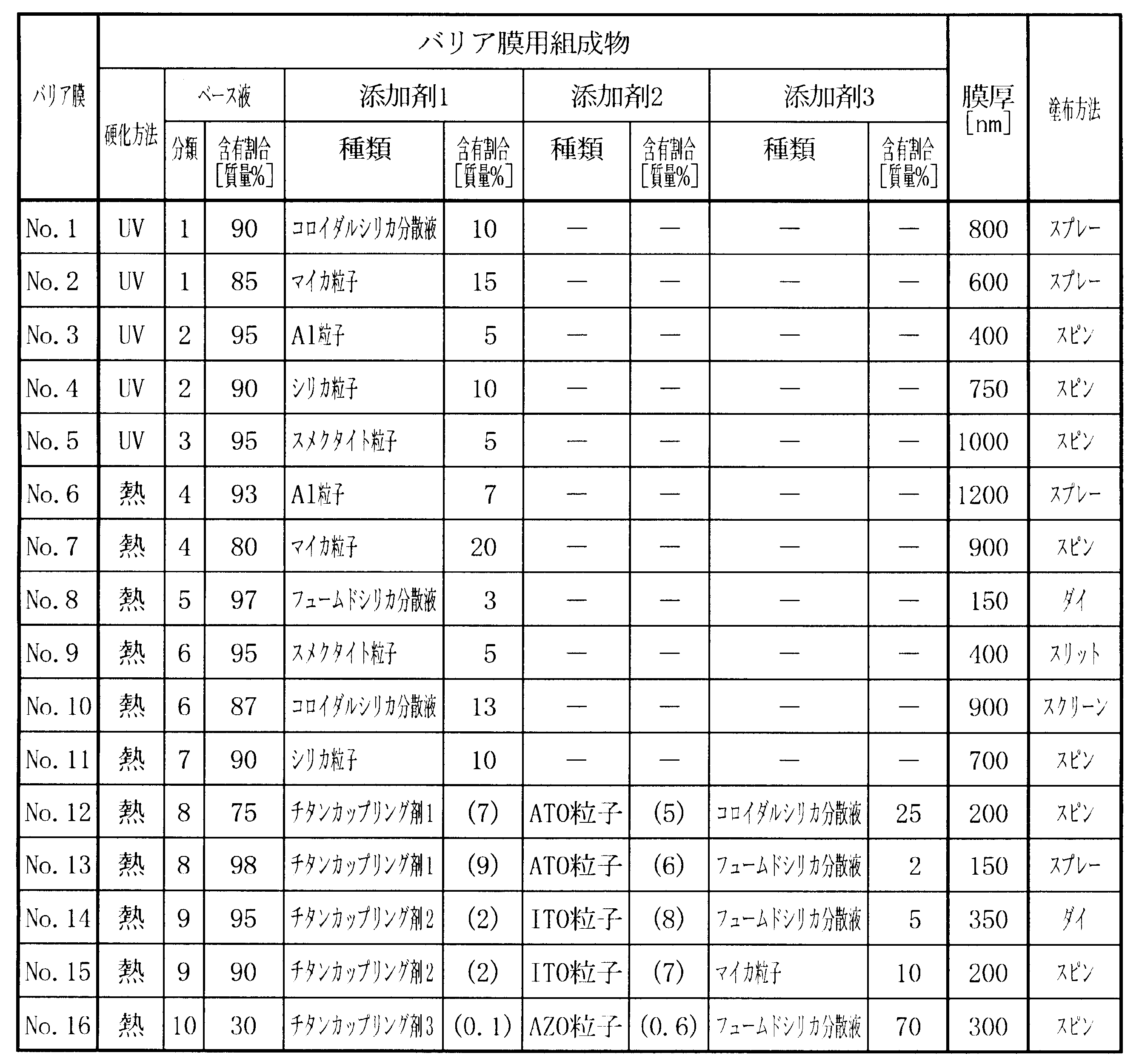

先ずIPA(イソプロピルアルコール)85質量%に平均粒径20nm程度のコロイダルシリカを15質量%混合して添加剤1となるコロイダルシリカ分散液を調製した。次いで分類1のアクリル系ベース液と上記コロイダルシリカ分散液とを混合し、攪拌羽根付きディスパーで500rpm程度の回転速度で5分間攪拌して補強膜用組成物である塗液を調製した。次にこの塗液(補強膜用組成物)をスプレーコーティング装置により、既に成膜が進んでいる太陽電池モジュールの裏面電極層(銀電極層)上に塗布して、硬化後の膜厚が500nmになるように補強膜用塗布層を形成した。更に真空乾燥により補強膜用塗布層から溶媒を脱離させた後に、紫外線照射装置により補強膜用塗布層に紫外線(UV)を照射して補強膜用塗布層をUV光硬化させ、裏面電極補強膜を得た。
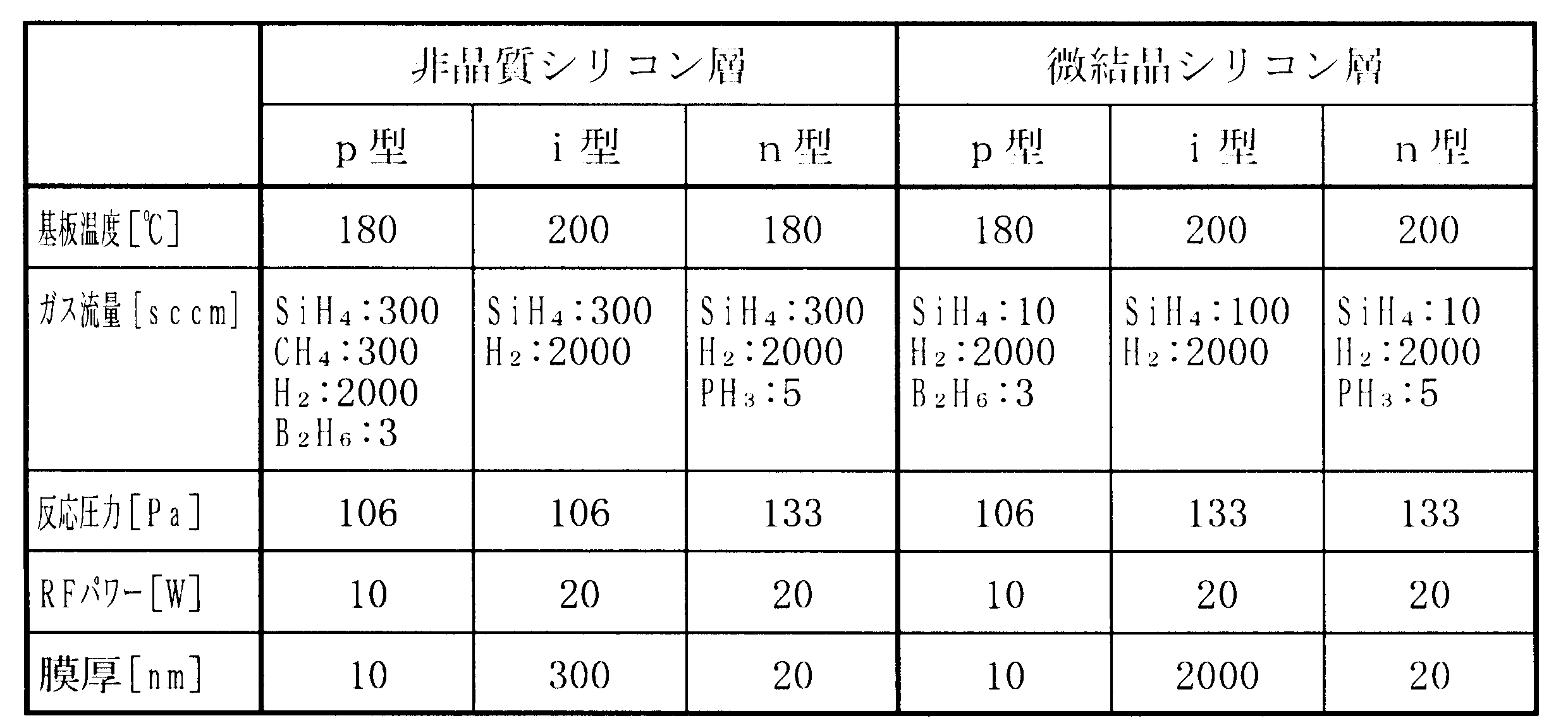
先ず分類1のアクリル系ベース液85質量%と、添加剤1として平均直径5μmかつ平均厚さ20nm程度のマイカ粒子(コープケミカル社製:ミクロマイカ)15質量%とを混合し、回転子により室温にて300rpm程度の回転速度で1時間攪拌して混合物を全体になじませた。次いで5000rpm程度まで高速回転可能なディスパー羽根を用いて上記混合物を攪拌し、マイカ粒子をベース液中に分散させて補強膜用組成物である塗液を調製した。次にこの塗液(補強膜用組成物)をスプレーコーティング装置により、既に成膜が進んでいる太陽電池モジュールの裏面電極層(銀電極層)上に塗布して、硬化後の膜厚が200nmになるように補強膜用塗布層を形成した。更に真空乾燥により補強膜用塗布層から溶媒を脱離させた後に、紫外線照射装置により補強膜用塗布層に紫外線(UV)を照射して補強膜用塗布層をUV光硬化させ、裏面電極補強膜を得た。上記以外は実施例1と同様に太陽電池モジュールを作製した。
先ず分類2のアクリル系ベース液95質量%と、添加剤1として平均直径35μmかつ平均厚さ100nm程度の扁平なAl粒子(東洋アルミニウム社製:アルペースト)5質量%とを混合し、回転子により室温にて300rpm程度の回転速度で1時間攪拌して混合物を全体になじませた。次いで2000rpm程度まで高速回転可能なディスパー羽根を用いて上記混合物を攪拌し、Al粒子をベース液中に分散させて補強膜用組成物である塗液を調製した。次にこの塗液(補強膜用組成物)をスピンコーティング装置により、既に成膜が進んでいる太陽電池モジュールの裏面電極層(銀電極層)上に塗布して、硬化後の膜厚が400nmになるように補強膜用塗布層を形成した。更に真空乾燥により補強膜用塗布層から溶媒を脱離させた後に、紫外線照射装置により補強膜用塗布層に紫外線(UV)を照射して補強膜用塗布層をUV光硬化させ、裏面電極補強膜を得た。上記以外は実施例1と同様に太陽電池モジュールを作製した。
先ず分類2のアクリル系ベース液90質量%と、添加剤1として平均粒径20nm程度のシリカ粒子(扶桑化学工業社製:シリカ)10質量%とを混合し、回転子により室温にて300rpm程度の回転速度で1時間攪拌して混合物を全体になじませた。次いで5000rpm程度まで高速回転可能なディスパー羽根を用いて上記混合物を攪拌し、シリカ粒子をベース液中に分散させて補強膜用組成物である塗液を調製した。次にこの塗液(補強膜用組成物)をスピンコーティング装置により、既に成膜が進んでいる太陽電池モジュールの裏面電極層(銀電極層)上に塗布して、硬化後の膜厚が300nmになるように補強膜用塗布層を形成した。更に真空乾燥により補強膜用塗布層から溶媒を脱離させた後に、紫外線照射装置により補強膜用塗布層に紫外線(UV)を照射して補強膜用塗布層をUV光硬化させ、裏面電極補強膜を得た。上記以外は実施例1と同様に太陽電池モジュールを作製した。
先ず分類3のアクリル系ベース液95質量%と、添加剤1として平均直径140nmかつ平均厚さ50nm程度の扁平なスメクタイト粒子(コープケミカル社製:合成スメクタイト)5質量%とを混合し、回転子により室温にて300rpm程度の回転速度で1時間攪拌して混合物を全体になじませた。次いで5000rpm程度まで高速回転可能なディスパー羽根を用いて上記混合物を攪拌し、スメクタイト粒子をベース液中に分散させて補強膜用組成物である塗液を調製した。次にこの塗液(補強膜用組成物)をスピンコーティング装置により、既に成膜が進んでいる太陽電池モジュールの裏面電極層(銀電極層)上に塗布して、硬化後の膜厚が150nmになるように補強膜用塗布層を形成した。更に真空乾燥により補強膜用塗布層から溶媒を脱離させた後に、紫外線照射装置により補強膜用塗布層に紫外線(UV)を照射して補強膜用塗布層をUV光硬化させ、裏面電極補強膜を得た。上記以外は実施例1と同様に太陽電池モジュールを作製した。
先ず分類4のエポキシ系ベース液93質量%と、添加剤1として平均直径27μmかつ平均厚さ100nm程度の扁平なAl粒子(東洋アルミニウム社製:アルペースト)とを混合し、回転子により室温にて300rpm程度の回転速度で1時間攪拌して混合物を全体になじませた。次いで2000rpmまで高速回転可能なディスパー羽根を用いて上記混合物を攪拌し、Al粒子をベース液中に分散させて補強膜用組成物である塗液を調製した。次にこの塗液(補強膜用組成物)をスプレーコーティング装置により、既に成膜が進んでいる太陽電池モジュールの裏面電極層(銀電極層)上に塗布して、硬化後の膜厚が400nmになるように補強膜用塗布層を形成した。更に室温で20分以上乾燥した後に、太陽電池モジュールを熱風乾燥炉内で150℃に20分間保持して補強膜用塗布層を熱硬化させ、裏面電極補強膜を得た。上記以外は実施例1と同様に太陽電池モジュールを作製した。
先ず分類4のエポキシ系ベース液80質量%と、添加剤1として平均直径1μmかつ平均厚さ20nm程度のマイカ粒子(コープケミカル社製:ミクロマイカ)20質量%とを混合し、回転子により室温にて300rpm程度の回転速度で1時間攪拌して混合物を全体になじませた。次いで5000rpm程度まで高速回転可能なディスパー羽根を用いて上記混合物を攪拌し、マイカ粒子をベース液中に分散させて補強膜用組成物である塗液を調製した。このとき塗液が70℃以上にならないように注意して羽根形状と回転速度を調整した。次にこの塗液(補強膜用組成物)をスピンコーティング装置により、既に成膜が進んでいる太陽電池モジュールの裏面電極層(銀電極層)上に塗布して、硬化後の膜厚が200nmになるように補強膜用塗布層を形成した。更に室温で20分以上乾燥した後に、太陽電池モジュールを熱風乾燥炉内で200℃に20分間保持して補強膜用塗布層を熱硬化させ、裏面電極補強膜を得た。上記以外は実施例1と同様に太陽電池モジュールを作製した。
先ず分類5のエポキシ系ベース液97質量%と、添加剤1としてフュームドシリカ分散液(日本アエロジル社製:アエロジル)3質量%とを混合し、超音波振動器により室温で10分間分散混合して混合物を全体になじませ、補強膜用組成物である塗液を調製した。次にこの塗液(補強膜用組成物)をダイコーティング装置により、既に成膜が進んでいる太陽電池モジュールの裏面電極層(銀電極層)上に塗布して、硬化後の膜厚が150nmになるように補強膜用塗布層を形成した。更に室温で20分以上乾燥した後に、太陽電池モジュールを熱風乾燥炉内で180℃に30分間保持して補強膜用塗布層を熱硬化させ、裏面電極補強膜を得た。なお、上記フュームドシリカ分散液は次のように調製した。先ずフュームドシリカ粒子10質量%と、IPA(イソプロピルアルコール)及びエタノールの混合溶媒(質量比2:1)90質量%とを混合した後に、室温にて800rpmの回転速度で1時間攪拌して混合物を調製した。次にこの混合物60gを100ccのガラス瓶中に入れ、直径0.3mmのジルコニアビーズ(昭和シェル石油社製:ミクロハイカ)100gを用いてペイントシェーカーで6時間分散することにより、導電性酸化物微粒子であるフュームドシリカ粒子の分散液を調製した。また上記以外は実施例1と同様に太陽電池モジュールを作製した。
先ず分類6のエポキシ系ベース液95質量%と、添加剤1として平均直径180nmかつ平均厚さ30nm程度の扁平なスメクタイト粒子(コープケミカル社製:合成スメクタイト)5質量%とを混合し、回転子により室温にて300rpm程度の回転速度で1時間攪拌して混合物を全体になじませた。次いで2000rpm程度まで高速回転可能なディスパー羽根を用いて攪拌し、Ti粒子をベース液中に分散させて補強膜用組成物である塗液を調製した。このとき塗液が70℃以上にならないように注意して羽根形状と回転数を調整した。次にこの塗液(補強膜用組成物)をスリットコーティング装置により、既に成膜が進んでいる太陽電池モジュールの裏面電極層(銀電極層)上に塗布して、硬化後の膜厚が400nmになるように補強膜用塗布層を形成した。更に室温で20分以上乾燥した後に、太陽電池モジュールを熱風乾燥炉内で200℃に20分間保持して補強膜用塗布層を熱硬化させ、裏面電極補強膜を得た。上記以外は実施例1と同様に太陽電池モジュールを作製した。
先ず分類6のエポキシ系ベース液87質量%と、添加剤1としてコロイダルシリカ分散液13質量%とを混合し、遊星攪拌装置により室温で10分間混合して混合物を全体になじませ、補強膜用組成物である塗液を調製した。次にこの塗液(補強膜用組成物)をスクリーン印刷装置により、既に成膜が進んでいる太陽電池モジュールの裏面電極層(銀電極層)上に塗布して、硬化後の膜厚が900nmになるように補強膜用塗布層を形成した。更に室温で20分以上乾燥した後に、太陽電池モジュールを熱風乾燥炉内で200℃に30分間保持して補強膜用塗布層を熱硬化させ、裏面電極補強膜を得た。なお、上記コロイダルシリカ分散液は実施例8のフュームドシリカ分散液と同様にして調製した。また上記以外は実施例1と同様に太陽電池モジュールを作製した。
先ず分類7のセルロース系ベース液90質量%と、添加剤1として平均粒径30nm程度のシリカ粒子(扶桑化学工業社製:シリカ)10質量%とを混合し、回転子により室温にて300rpm程度の回転速度で1時間攪拌して混合物を全体になじませた。次いで5000rpm程度まで高速回転可能なディスパー羽根を用いて上記混合物を攪拌し、シリカ粒子をベース液中に分散させて補強膜用組成物である塗液を調製した。次にこの塗液(補強膜用組成物)をスピンコーティング装置により、既に成膜が進んでいる太陽電池モジュールの裏面電極層(銀電極層)上に塗布して、硬化後の膜厚が400nmになるように補強膜用塗布層を形成した。更に室温で20分以上乾燥した後に、太陽電池モジュールを熱風乾燥炉内で180℃に20分間保持して補強膜用塗布層を熱硬化させ、裏面電極補強膜を得た。上記以外は実施例1と同様に太陽電池モジュールを作製した。
先ずIPA(イソプロピルアルコール)85質量%に平均粒径20nm程度のコロイダルシリカを15質量%混合して添加剤3となるコロイダルシリカ分散液(日産化学社製:スノーテックス20)を調製した。次いで分類8のSiO2結合剤系ベース液75質量%と上記コロイダルシリカ分散液25質量%とを混合し、超音波振動器により室温で10分間分散混合して混合物を全体になじませ、補強膜用組成物である塗液を調製した。次にこの塗液(補強膜用組成物)をスピンコーティング装置により、既に成膜が進んでいる太陽電池モジュールの裏面電極層(銀電極層)上に塗布して、硬化後の膜厚が200nmになるように補強膜用塗布層を形成した。更に真空乾燥により補強膜用塗布層から溶媒を離脱させた後に、太陽電池モジュールを熱風乾燥炉内で200℃に30分間保持して補強膜用塗布層を熱硬化させ、裏面電極補強膜を得た。なお、表6において、添加剤1のチタンカップリング剤1と添加剤2のATO(酸化アンチモン-酸化錫系複合酸化物)粒子はベース液中に既に含まれているため、これらの添加量は塗液(補強膜用組成物)全体を100質量%としたときの割合(カッコ付きの数値)で示した。また上記以外は実施例1と同様に太陽電池モジュールを作製した。
先ず分類8のSiO2結合剤系ベース液98質量%と、添加剤3としてフュームドシリカ分散液2質量%とを混合し、超音波振動器により室温にて10分間分散混合して混合物を全体になじませ、補強膜用組成物である塗液を調製した。次にこの塗液(補強膜用組成物)をスプレーコーティング装置により、既に成膜が進んでいる太陽電池モジュールの裏面電極層(銀電極層)上に塗布して、硬化後の膜厚が150nmになるように補強膜用塗布層を形成した。更に真空乾燥により補強膜用塗布層から溶媒を離脱させた後に、太陽電池モジュールを熱風乾燥炉内で150℃に20分間保持して補強膜用塗布層を熱硬化させ、裏面電極補強膜を得た。なお、表6において、添加剤1のチタンカップリング剤1と添加剤2のATO(酸化アンチモン-酸化錫系複合酸化物)粒子はベース液中に既に含まれているため、これらの添加量は塗液(補強膜用組成物)全体を100質量%としたときの割合(カッコ付きの数値)で示した。また上記フュームドシリカ分散液は実施例8のフュームドシリカ分散液と同様にして調製した。また上記以外は実施例1と同様に太陽電池モジュールを作製した。
先ず分類9のSiO2結合剤系ベース液95質量%と、添加剤3としてフュームドシリカ分散液5質量%とを混合し、超音波振動器により室温にて10分間分散混合して混合物を全体になじませ、補強膜用組成物である塗液を調製した。次にこの塗液(補強膜用組成物)をダイコーティング装置により、既に成膜が進んでいる太陽電池モジュールの裏面電極層(銀電極層)上に塗布して、硬化後の膜厚が350nmになるように補強膜用塗布層を形成した。更に真空乾燥により補強膜用塗布層から溶媒を離脱させた後に、太陽電池モジュールを熱風乾燥炉内で180℃に20分間保持して補強膜用塗布層を熱硬化させ、裏面電極補強膜を得た。なお、表6において、添加剤1のチタンカップリング剤2と添加剤2のITO(酸化インジウム-酸化錫系複合酸化物)粒子はベース液中に既に含まれているため、これらの添加量は塗液(補強膜用組成物)全体を100質量%としたときの割合(カッコ付きの数値)で示した。また上記フュームドシリカ分散液は実施例8のフュームドシリカ分散液と同様にして調製した。また上記以外は実施例1と同様に太陽電池モジュールを作製した。
先ず分類9のSiO2結合剤系ベース液90質量%と、添加剤3として平均直径5μmかつ平均厚さ20nm程度のマイカ粒子(コープケミカル社製:ミクロマイカ)10質量%とを混合し、回転子により室温にて300rpm程度の回転速度で1時間攪拌して混合物を全体になじませた。次いで5000rpm程度まで高速回転可能なディスパー羽根を用いて上記混合物を攪拌し、マイカ粒子をベース液中に分散させて補強膜用組成物である塗液を調製した。このとき塗液が70℃以上にならないように注意して羽根形状と回転速度を調整した。次にこの塗液(補強膜用組成物)をスピンコーティング装置により、既に成膜が進んでいる太陽電池モジュールの裏面電極層(銀電極層)上に塗布して、硬化後の膜厚が200nmになるように補強膜用塗布層を形成した。更に室温で20分以上乾燥した後に、太陽電池モジュールを熱風乾燥炉内で200℃に30分間保持して補強膜用塗布層を熱硬化させ、裏面電極補強膜を得た。なお、表6において、添加剤1のチタンカップリング剤2と添加剤2のITO(酸化インジウム-酸化錫系複合酸化物)粒子はベース液中に既に含まれているため、これらの添加量は塗液(補強膜用組成物)全体を100質量%としたときの割合(カッコ付きの数値)で示した。また上記以外は実施例1と同様に太陽電池モジュールを作製した。
先ず分類1のアクリル系ベース液96質量%と、添加剤1として平均直径35μmかつ平均厚さ100nm程度のAl粒子(東洋アルミニウム社製:アルペースト)4質量%とを混合し、回転子により室温にて300rpm程度の回転速度で1時間攪拌して混合物を全体になじませた。次いで2000rpm程度まで高速回転可能なディスパー羽根を用いて上記混合物を攪拌し、Al粒子をベース液中に分散させて補強膜用組成物である塗液を調製した。次にこの塗液(補強膜用組成物)をダイコーティング装置により、既に成膜が進んでいる太陽電池モジュールの裏面電極層(銀電極層)上に塗布して、硬化後の膜厚が250nmになるように補強膜用塗布層を形成した。更に真空乾燥により補強膜用塗布層から溶媒を脱離させ、紫外線照射装置により補強膜用塗布層に紫外線(UV)を照射して補強膜用塗布層をUV光硬化させた後に、太陽電池モジュールを熱風乾燥炉内で70℃に3時間保持して熱硬化させることにより、十分に硬化した裏面電極補強膜を得た。なお、この実施例では、発電層は、基板側から順にp型a-Si(非晶質シリコン)、i型a-Si及びn型a-Siが積層した非晶質シリコン層1層からなる光電変換ユニットとした。また上記以外は実施例1と同様に太陽電池モジュールを作製した。
先ずIPA(イソプロピルアルコール)85質量%に平均粒径20nm程度のコロイダルシリカを15質量%混合して添加剤1となるコロイダルシリカ分散液(日産化学社製:IPA-ST)を調製した。次いで分類1のアクリル系ベース液93質量%と上記コロイダルシリカ分散液7質量%とを混合し、超音波振動器により室温で10分間分散混合して混合物を全体になじませ、補強膜用組成物である塗液を調製した。次にこの塗液(補強膜用組成物)をスピンコーティング装置により、既に成膜が進んでいる太陽電池モジュールの裏面電極層(銀電極層)上に塗布して、硬化後の膜厚が400nmになるように補強膜用塗布層を形成した。更に真空乾燥により補強膜用塗布層から溶媒を脱離させ、紫外線照射装置により補強膜用塗布層に紫外線(UV)を照射して補強膜用塗布層をUV光硬化させた後に、太陽電池モジュールを熱風乾燥炉内で70℃に3時間保持して熱硬化させることにより、十分に硬化した裏面電極補強膜を得た。なお、この実施例では、発電層は、基板側から順にp型μc-Si(微結晶シリコン)、i型μc-Si及びn型μc-Siが積層した微結晶シリコン層1層からなる光電変換ユニットとした。また上記以外は実施例1と同様に太陽電池モジュールを作製した。
既に成膜が進んでいる太陽電池モジュールの裏面電極層(銀電極層)上に裏面電極補強膜を形成しなかった。この太陽電池モジュールを比較例1とした。
既に成膜が進んでいる太陽電池モジュールの裏面電極層(銀電極層)上にスパッタ法でTi(チタン)を蒸着することにより厚さ15nmの裏面電極補強膜(Ti層)を形成した。この太陽電池モジュールを比較例2とした。
既に成膜が進んでいる太陽電池モジュールの裏面電極層(銀電極層)上にスパッタ法でAl(アルミニウム)を蒸着することにより厚さ200nmの裏面電極補強膜(Al層)を形成した。この太陽電池モジュールを比較例3とした。
実施例1~17及び比較例1~3の太陽電池モジュールについてバリの発生、密着性及び相対出力特性を評価した。先ずバリの発生は、太陽電池モジュールに対してレーザ加工法によるレーザスクライブを実施した際に、分離溝の内面(加工面)へのバリの発生の程度や、分離溝の幅のガタツキの程度を優、良、可及び不可の4段階で評価した。分離溝の加工ラインが安定して綺麗なものを『優』とした。そして、分離溝の一部にうねりなどが見られたけれども大きな凹凸やはみ出し部がなかったものを『良』とした。また分離溝全体にライン幅が安定せず加工ラインが常にガタガタと凹凸がみられたけれどもライン間に必ず隙間がありショートしている部分が見られなかったものを『可』とした。更に、分離溝の加工ラインの凹凸が非常に大きく、ライン間が切れておらずショートを引き起こし兼ねない状況のものや、ライン幅以上に広い削りかすがライン上に強固に残っていたものを『不可』とした。


先ずIPA(イソプロピルアルコール)85質量%に平均粒径20nm程度のコロイダルシリカを15質量%混合して添加剤1となるコロイダルシリカ分散液を調製した。次いで分類1のアクリル系ベース液と上記コロイダルシリカ分散液とを混合し、攪拌羽根付きディスパーで500rpm程度の回転速度で5分間攪拌して補強膜用組成物である塗液を調製した。次にこの塗液(補強膜用組成物)をスプレーコーティング装置により、既に成膜が進んでいる太陽電池モジュールの裏面電極層(銀電極層)上に塗布して、硬化後の膜厚が500nmになるように補強膜用塗布層を形成した。更に真空乾燥により補強膜用塗布層から溶媒を脱離させた後に、紫外線照射装置により補強膜用塗布層に紫外線(UV)を照射して補強膜用塗布層をUV光硬化させ、裏面電極補強膜を得た。
先ず分類1のアクリル系ベース液85質量%と、添加剤1として平均直径5μmかつ平均厚さ20nm程度のマイカ粒子(コープケミカル社製:ミクロマイカ)15質量%とを混合し、回転子により室温にて300rpm程度の回転速度で1時間攪拌して混合物を全体になじませた。次いで5000rpm程度まで高速回転可能なディスパー羽根を用いて上記混合物を攪拌し、マイカ粒子をベース液中に分散させて補強膜用組成物である塗液を調製した。次にこの塗液(補強膜用組成物)をスプレーコーティング装置により、既に成膜が進んでいる太陽電池モジュールの裏面電極層(銀電極層)上に塗布して、硬化後の膜厚が200nmになるように補強膜用塗布層を形成した。更に真空乾燥により補強膜用塗布層から溶媒を脱離させた後に、紫外線照射装置により補強膜用塗布層に紫外線(UV)を照射して補強膜用塗布層をUV光硬化させ、裏面電極補強膜を得た。上記以外は実施例18と同様に太陽電池モジュールを作製した。
先ず分類2のアクリル系ベース液95質量%と、添加剤1として平均直径35μmかつ平均厚さ100nm程度の扁平なAl粒子(東洋アルミニウム社製:アルペースト)5質量%とを混合し、回転子により室温にて300rpm程度の回転速度で1時間攪拌して混合物を全体になじませた。次いで2000rpm程度まで高速回転可能なディスパー羽根を用いて上記混合物を攪拌し、Al粒子をベース液中に分散させて補強膜用組成物である塗液を調製した。次にこの塗液(補強膜用組成物)をスピンコーティング装置により、既に成膜が進んでいる太陽電池モジュールの裏面電極層(銀電極層)上に塗布して、硬化後の膜厚が400nmになるように補強膜用塗布層を形成した。更に真空乾燥により補強膜用塗布層から溶媒を脱離させた後に、紫外線照射装置により補強膜用塗布層に紫外線(UV)を照射して補強膜用塗布層をUV光硬化させ、裏面電極補強膜を得た。上記以外は実施例18と同様に太陽電池モジュールを作製した。
先ず分類2のアクリル系ベース液90質量%と、添加剤1として平均粒径20nm程度のシリカ粒子(扶桑化学工業社製:シリカ)10質量%とを混合し、回転子により室温にて300rpm程度の回転速度で1時間攪拌して混合物を全体になじませた。次いで5000rpm程度まで高速回転可能なディスパー羽根を用いて上記混合物を攪拌し、シリカ粒子をベース液中に分散させて補強膜用組成物である塗液を調製した。次にこの塗液(補強膜用組成物)をスピンコーティング装置により、既に成膜が進んでいる太陽電池モジュールの裏面電極層(銀電極層)上に塗布して、硬化後の膜厚が300nmになるように補強膜用塗布層を形成した。更に真空乾燥により補強膜用塗布層から溶媒を脱離させた後に、紫外線照射装置により補強膜用塗布層に紫外線(UV)を照射して補強膜用塗布層をUV光硬化させ、裏面電極補強膜を得た。上記以外は実施例18と同様に太陽電池モジュールを作製した。
先ず分類3のアクリル系ベース液95質量%と、添加剤1として平均直径140nmかつ平均厚さ50nm程度の扁平なスメクタイト粒子(コープケミカル社製:合成スメクタイト)5質量%とを混合し、回転子により室温にて300rpm程度の回転速度で1時間攪拌して混合物を全体になじませた。次いで5000rpm程度まで高速回転可能なディスパー羽根を用いて上記混合物を攪拌し、スメクタイト粒子をベース液中に分散させて補強膜用組成物である塗液を調製した。次にこの塗液(補強膜用組成物)をスピンコーティング装置により、既に成膜が進んでいる太陽電池モジュールの裏面電極層(銀電極層)上に塗布して、硬化後の膜厚が150nmになるように補強膜用塗布層を形成した。更に真空乾燥により補強膜用塗布層から溶媒を脱離させた後に、紫外線照射装置により補強膜用塗布層に紫外線(UV)を照射して補強膜用塗布層をUV光硬化させ、裏面電極補強膜を得た。上記以外は実施例18と同様に太陽電池モジュールを作製した。
先ず分類4のエポキシ系ベース液93質量%と、添加剤1として平均直径27μmかつ平均厚さ100nm程度の扁平なAl粒子(東洋アルミニウム社製:アルペースト)とを混合し、回転子により室温にて300rpm程度の回転速度で1時間攪拌して混合物を全体になじませた。次いで2000rpmまで高速回転可能なディスパー羽根を用いて上記混合物を攪拌し、Al粒子をベース液中に分散させて補強膜用組成物である塗液を調製した。次にこの塗液(補強膜用組成物)をスプレーコーティング装置により、既に成膜が進んでいる太陽電池モジュールの裏面電極層(銀電極層)上に塗布して、硬化後の膜厚が400nmになるように補強膜用塗布層を形成した。更に室温で20分以上乾燥した後に、太陽電池モジュールを熱風乾燥炉内で150℃に20分間保持して補強膜用塗布層を熱硬化させ、裏面電極補強膜を得た。上記以外は実施例18と同様に太陽電池モジュールを作製した。
先ず分類4のエポキシ系ベース液80質量%と、添加剤1として平均直径1μmかつ平均厚さ20nm程度のマイカ粒子(コープケミカル社製:ミクロマイカ)20質量%とを混合し、回転子により室温にて300rpm程度の回転速度で1時間攪拌して混合物を全体になじませた。次いで5000rpm程度まで高速回転可能なディスパー羽根を用いて上記混合物を攪拌し、マイカ粒子をベース液中に分散させて補強膜用組成物である塗液を調製した。このとき塗液が70℃以上にならないように注意して羽根形状と回転速度を調整した。次にこの塗液(補強膜用組成物)をスピンコーティング装置により、既に成膜が進んでいる太陽電池モジュールの裏面電極層(銀電極層)上に塗布して、硬化後の膜厚が200nmになるように補強膜用塗布層を形成した。更に室温で20分以上乾燥した後に、太陽電池モジュールを熱風乾燥炉内で200℃に20分間保持して補強膜用塗布層を熱硬化させ、裏面電極補強膜を得た。上記以外は実施例18と同様に太陽電池モジュールを作製した。
先ず分類5のエポキシ系ベース液97質量%と、添加剤1としてフュームドシリカ分散液(日本アエロジル社製:アエロジル)3質量%とを混合し、超音波振動器により室温で10分間分散混合して混合物を全体になじませ、補強膜用組成物である塗液を調製した。次にこの塗液(補強膜用組成物)をダイコーティング装置により、既に成膜が進んでいる太陽電池モジュールの裏面電極層(銀電極層)上に塗布して、硬化後の膜厚が150nmになるように補強膜用塗布層を形成した。更に室温で20分以上乾燥した後に、太陽電池モジュールを熱風乾燥炉内で180℃に30分間保持して補強膜用塗布層を熱硬化させ、裏面電極補強膜を得た。なお、上記フュームドシリカ分散液は次のように調製した。先ずフュームドシリカ粒子10質量%と、IPA(イソプロピルアルコール)及びエタノールの混合溶媒(質量比2:1)90質量%とを混合した後に、室温にて800rpmの回転速度で1時間攪拌して混合物を調製した。次にこの混合物60gを100ccのガラス瓶中に入れ、直径0.3mmのジルコニアビーズ(昭和シェル石油社製:ミクロハイカ)100gを用いてペイントシェーカーで6時間分散することにより、導電性酸化物微粒子であるフュームドシリカ粒子の分散液を調製した。上記以外は実施例18と同様に太陽電池モジュールを作製した。
先ず分類6のエポキシ系ベース液95質量%と、添加剤1として平均直径180nmかつ平均厚さ30nm程度の扁平なスメクタイト粒子(コープケミカル社製:合成スメクタイト)5質量%とを混合し、回転子により室温にて300rpm程度の回転速度で1時間攪拌して混合物を全体になじませた。次いで2000rpm程度まで高速回転可能なディスパー羽根を用いて攪拌し、Ti粒子をベース液中に分散させて補強膜用組成物である塗液を調製した。このとき塗液が70℃以上にならないように注意して羽根形状と回転数を調整した。次にこの塗液(補強膜用組成物)をスリットコーティング装置により、既に成膜が進んでいる太陽電池モジュールの裏面電極層(銀電極層)上に塗布して、硬化後の膜厚が400nmになるように補強膜用塗布層を形成した。更に室温で20分以上乾燥した後に、太陽電池モジュールを熱風乾燥炉内で200℃に20分間保持して補強膜用塗布層を熱硬化させ、裏面電極補強膜を得た。上記以外は実施例18と同様に太陽電池モジュールを作製した。
先ず分類6のエポキシ系ベース液87質量%と、添加剤1としてコロイダルシリカ分散液13質量%とを混合し、遊星攪拌装置により室温で10分間混合して混合物を全体になじませ、補強膜用組成物である塗液を調製した。次にこの塗液(補強膜用組成物)をスクリーン印刷装置により、既に成膜が進んでいる太陽電池モジュールの裏面電極層(銀電極層)上に塗布して、硬化後の膜厚が900nmになるように補強膜用塗布層を形成した。更に室温で20分以上乾燥した後に、太陽電池モジュールを熱風乾燥炉内で200℃に30分間保持して補強膜用塗布層を熱硬化させ、裏面電極補強膜を得た。なお、上記コロイダルシリカ分散液は実施例25のフュームドシリカ分散液と同様にして調製した。また上記以外は実施例18と同様に太陽電池モジュールを作製した。
先ず分類7のセルロース系ベース液90質量%と、添加剤1として平均粒径30nm程度のシリカ粒子(扶桑化学工業社製:シリカ)10質量%とを混合し、回転子により室温にて300rpm程度の回転速度で1時間攪拌して混合物を全体になじませた。次いで5000rpm程度まで高速回転可能なディスパー羽根を用いて上記混合物を攪拌し、シリカ粒子をベース液中に分散させて補強膜用組成物である塗液を調製した。次にこの塗液(補強膜用組成物)をスピンコーティング装置により、既に成膜が進んでいる太陽電池モジュールの裏面電極層(銀電極層)上に塗布して、硬化後の膜厚が400nmになるように補強膜用塗布層を形成した。更に室温で20分以上乾燥した後に、太陽電池モジュールを熱風乾燥炉内で180℃に20分間保持して補強膜用塗布層を熱硬化させ、裏面電極補強膜を得た。上記以外は実施例18と同様に太陽電池モジュールを作製した。
先ずIPA(イソプロピルアルコール)85質量%に平均粒径20nm程度のコロイダルシリカを15質量%混合して添加剤3となるコロイダルシリカ分散液(日産化学社製:スノーテックス20)を調製した。次いで分類8のSiO2結合剤系ベース液75質量%と上記コロイダルシリカ分散液25質量%とを混合し、超音波振動器により室温で10分間分散混合して混合物を全体になじませ、補強膜用組成物である塗液を調製した。次にこの塗液(補強膜用組成物)をスピンコーティング装置により、既に成膜が進んでいる太陽電池モジュールの裏面電極層(銀電極層)上に塗布して、硬化後の膜厚が200nmになるように補強膜用塗布層を形成した。更に真空乾燥により補強膜用塗布層から溶媒を離脱させた後に、太陽電池モジュールを熱風乾燥炉内で200℃に30分間保持して補強膜用塗布層を熱硬化させ、裏面電極補強膜を得た。なお、表6において、添加剤1のチタンカップリング剤1と添加剤2のATO(酸化アンチモン-酸化錫系複合酸化物)粒子はベース液中に既に含まれているため、これらの添加量は塗液(補強膜用組成物)全体を100質量%としたときの割合(カッコ付きの数値)で示した。また上記以外は実施例18と同様に太陽電池モジュールを作製した。
先ず分類8のSiO2結合剤系ベース液98質量%と、添加剤3としてフュームドシリカ分散液2質量%とを混合し、超音波振動器により室温にて10分間分散混合して混合物を全体になじませ、補強膜用組成物である塗液を調製した。次にこの塗液(補強膜用組成物)をスプレーコーティング装置により、既に成膜が進んでいる太陽電池モジュールの裏面電極層(銀電極層)上に塗布して、硬化後の膜厚が150nmになるように補強膜用塗布層を形成した。更に真空乾燥により補強膜用塗布層から溶媒を離脱させた後に、太陽電池モジュールを熱風乾燥炉内で150℃に20分間保持して補強膜用塗布層を熱硬化させ、裏面電極補強膜を得た。なお、表6において、添加剤1のチタンカップリング剤1と添加剤2のATO(酸化アンチモン-酸化錫系複合酸化物)粒子はベース液中に既に含まれているため、これらの添加量は塗液(補強膜用組成物)全体を100質量%としたときの割合(カッコ付きの数値)で示した。また上記フュームドシリカ分散液は実施例25のフュームドシリカ分散液と同様にして調製した。更に上記以外は実施例18と同様に太陽電池モジュールを作製した。
先ず分類9のSiO2結合剤系ベース液95質量%と、添加剤3としてフュームドシリカ分散液5質量%とを混合し、超音波振動器により室温にて10分間分散混合して混合物を全体になじませ、補強膜用組成物である塗液を調製した。次にこの塗液(補強膜用組成物)をダイコーティング装置により、既に成膜が進んでいる太陽電池モジュールの裏面電極層(銀電極層)上に塗布して、硬化後の膜厚が350nmになるように補強膜用塗布層を形成した。更に真空乾燥により補強膜用塗布層から溶媒を離脱させた後に、太陽電池モジュールを熱風乾燥炉内で180℃に20分間保持して補強膜用塗布層を熱硬化させ、裏面電極補強膜を得た。なお、表6において、添加剤1のチタンカップリング剤2と添加剤2のITO(酸化インジウム-酸化錫系複合酸化物)粒子はベース液中に既に含まれているため、これらの添加量は塗液(補強膜用組成物)全体を100質量%としたときの割合(カッコ付きの数値)で示した。また上記フュームドシリカ分散液は実施例25のフュームドシリカ分散液と同様にして調製した。更に上記以外は実施例18と同様に太陽電池モジュールを作製した。
先ず分類9のSiO2結合剤系ベース液90質量%と、添加剤3として平均直径5μmかつ平均厚さ20nm程度のマイカ粒子(コープケミカル社製:ミクロマイカ)10質量%とを混合し、回転子により室温にて300rpm程度の回転速度で1時間攪拌して混合物を全体になじませた。次いで5000rpm程度まで高速回転可能なディスパー羽根を用いて上記混合物を攪拌し、マイカ粒子をベース液中に分散させて補強膜用組成物である塗液を調製した。このとき塗液が70℃以上にならないように注意して羽根形状と回転速度を調整した。次にこの塗液(補強膜用組成物)をスピンコーティング装置により、既に成膜が進んでいる太陽電池モジュールの裏面電極層(銀電極層)上に塗布して、硬化後の膜厚が200nmになるように補強膜用塗布層を形成した。更に室温で20分以上乾燥した後に、太陽電池モジュールを熱風乾燥炉内で200℃に30分間保持して補強膜用塗布層を熱硬化させ、裏面電極補強膜を得た。なお、表6において、添加剤1のチタンカップリング剤2と添加剤2のITO(酸化インジウム-酸化錫系複合酸化物)粒子はベース液中に既に含まれているため、これらの添加量は塗液(補強膜用組成物)全体を100質量%としたときの割合(カッコ付きの数値)で示した。また上記以外は実施例18と同様に太陽電池モジュールを作製した。
先ず分類1のアクリル系ベース液96質量%と、添加剤1として平均直径35μmかつ平均厚さ100nm程度のAl粒子(東洋アルミニウム社製:アルペースト)4質量%とを混合し、回転子により室温にて300rpm程度の回転速度で1時間攪拌して混合物を全体になじませた。次いで2000rpm程度まで高速回転可能なディスパー羽根を用いて上記混合物を攪拌し、Al粒子をベース液中に分散させて補強膜用組成物である塗液を調製した。次にこの塗液(補強膜用組成物)をダイコーティング装置により、既に成膜が進んでいる太陽電池モジュールの裏面電極層(銀電極層)上に塗布して、硬化後の膜厚が250nmになるように補強膜用塗布層を形成した。更に真空乾燥により補強膜用塗布層から溶媒を脱離させ、紫外線照射装置により補強膜用塗布層に紫外線(UV)を照射して補強膜用塗布層をUV光硬化させた後に、太陽電池モジュールを熱風乾燥炉内で70℃に3時間保持して熱硬化させることにより、十分に硬化した裏面電極補強膜を得た。なお、この実施例では、発電層は、基板側から順にp型a-Si(非晶質シリコン)、i型a-Si及びn型a-Siが積層した非晶質シリコン層1層からなる光電変換ユニットとした。また上記以外は実施例18と同様に太陽電池モジュールを作製した。
先ずIPA(イソプロピルアルコール)85質量%に平均粒径20nm程度のコロイダルシリカを15質量%混合して添加剤1となるコロイダルシリカ分散液(日産化学社製:IPA-ST)を調製した。次いで分類1のアクリル系ベース液93質量%と上記コロイダルシリカ分散液7質量%とを混合し、超音波振動器により室温で10分間分散混合して混合物を全体になじませ、補強膜用組成物である塗液を調製した。次にこの塗液(補強膜用組成物)をスピンコーティング装置により、既に成膜が進んでいる太陽電池モジュールの裏面電極層(銀電極層)上に塗布して、硬化後の膜厚が400nmになるように補強膜用塗布層を形成した。更に真空乾燥により補強膜用塗布層から溶媒を脱離させ、紫外線照射装置により補強膜用塗布層に紫外線(UV)を照射して補強膜用塗布層をUV光硬化させた後に、太陽電池モジュールを熱風乾燥炉内で70℃に3時間保持して熱硬化させることにより、十分に硬化した裏面電極補強膜を得た。なお、この実施例では、発電層は、基板側から順にp型μc-Si(微結晶シリコン)、i型μc-Si及びn型μc-Siが積層した微結晶シリコン層1層からなる光電変換ユニットとした。また上記以外は実施例18と同様に太陽電池モジュールを作製した。
既に成膜が進んでいる太陽電池モジュール上、即ち光電変換ユニット上に湿式塗工法により透明導電膜及び裏面電極層を形成した太陽電池モジュール上に、裏面電極補強膜を形成しなかった。この太陽電池モジュールを比較例4とした。
既に成膜が進んでいる太陽電池モジュール上、即ち光電変換ユニット上に湿式塗工法により透明導電膜及び裏面電極層を形成した太陽電池モジュール上に、スパッタ法でTi(チタン)を蒸着することにより厚さ15nmの裏面電極補強膜(Ti層)を形成した。この太陽電池モジュールを比較例5とした。
既に成膜が進んでいる太陽電池モジュール上、即ち光電変換ユニット上に湿式塗工法により透明導電膜及び裏面電極層を形成した太陽電池モジュール上に、スパッタ法でAl(アルミニウム)を蒸着することにより厚さ200nmの裏面電極補強膜(Al層)を形成した。この太陽電池モジュールを比較例6とした。
実施例18~34及び比較例4~6の太陽電池モジュールについてバリの発生、密着性及び相対出力特性を評価した。先ずバリの発生は、太陽電池モジュールに対してレーザ加工法によるレーザスクライブを実施した際に、分離溝の内面(加工面)へのバリの発生の程度や、分離溝の幅のガタツキの程度を優、良、可及び不可の4段階で評価した。分離溝の加工ラインが安定して綺麗なものを『優』とした。そして、分離溝の一部にうねりなどが見られたけれども大きな凹凸やはみ出し部がなかったものを『良』とした。また分離溝全体にライン幅が安定せず加工ラインが常にガタガタと凹凸がみられたけれどもライン間に必ず隙間がありショートしている部分が見られなかったものを『可』とした。更に、分離溝の加工ラインの凹凸が非常に大きく、ライン間が切れておらずショートを引き起こし兼ねない状況のものや、ライン幅以上に広い削りかすがライン上に強固に残っていたものを『不可』とした。
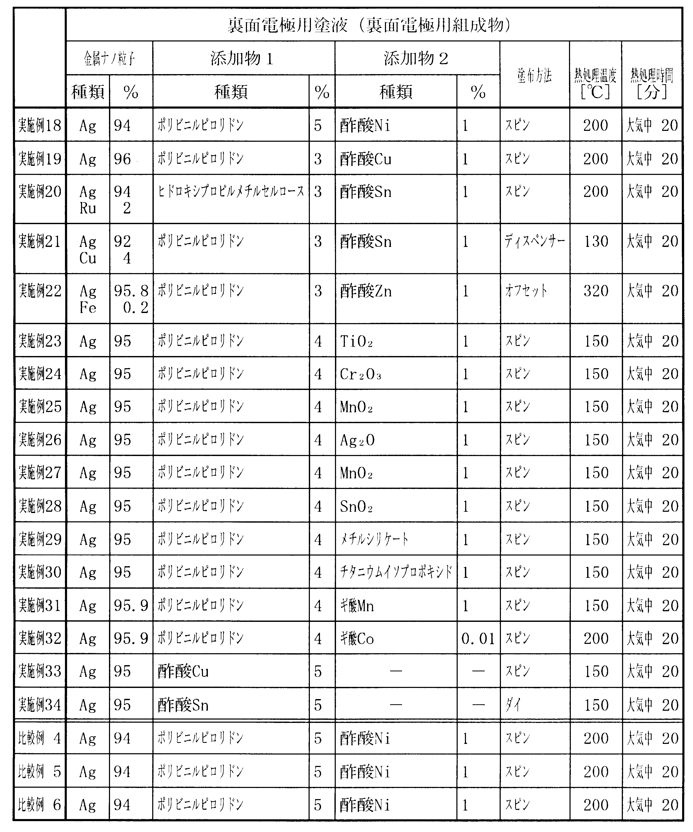

先ず、図4に示すように、既に成膜が進んでいる太陽電池モジュールの裏面電極層16(銀電極層)上に、上記表2の補強膜No.12による補強膜17を形成した。次いで、後述する光電変換ユニット13のパターニング位置(分離溝23)から50μm横の位置に、基板11側からレーザを照射してパターニングした。即ち、光電変換ユニット13、透明導電膜14、裏面電極16および裏面電極補強膜17を爆裂するレーザスクライブにより、補強膜17の表面から表面電極層12へ延びる分離溝18を形成することにより短冊状に分離加工した。レーザスクライブによる分離加工(分離溝18の形成)には、エネルギー密度0.7J/cm3、パルス周波数4kHzのNd:YAGレーザを用いた。最後に、分離溝18を埋めるとともに、補強膜17上に上記表3のバリア膜No.1による単一のバリア膜を形成した。この太陽電池モジュールを実施例35とした。
次の表10に示すように、補強膜No.1により補強膜を形成し、バリア膜No.12によりバリア膜を形成したこと以外は、実施例35と同様に太陽電池モジュールを形成した。
次の表10に示すように、補強膜No.13により補強膜を形成し、バリア膜No.4によりバリア膜を形成したこと以外は、実施例35と同様に太陽電池モジュールを形成した。
次の表10に示すように、補強膜No.7により補強膜を形成し、バリア膜No.7によりバリア膜を形成したこと以外は、実施例35と同様に太陽電池モジュールを形成した。
次の表10に示すように、補強膜No.2により補強膜を形成し、バリア膜No.14によりバリア膜を形成したこと以外は、実施例35と同様に太陽電池モジュールを形成した。
次の表10に示すように、補強膜No.3により補強膜を形成し、バリア膜No.16を成膜した後、更にバリア膜No.1を重ねて成膜して2層からなるバリア膜を形成したこと以外は、実施例35と同様に太陽電池モジュールを形成した。
次の表10に示すように、補強膜No.8により補強膜を形成し、バリア膜No.14を成膜した後、更にバリア膜No.6を重ねて成膜して2層からなるバリア膜を形成したこと以外は、実施例35と同様に太陽電池モジュールを形成した。
次の表10に示すように、補強膜No.10により補強膜を形成し、バリア膜No.15を成膜した後、更にバリア膜No.7を重ねて成膜して2層からなるバリア膜を形成したこと以外は、実施例35と同様に太陽電池モジュールを形成した。
次の表10に示すように、補強膜No.16により補強膜を形成し、バリア膜No.13を成膜した後、更にバリア膜No.10を重ねて成膜して2層からなるバリア膜を形成したこと以外は、実施例35と同様に太陽電池モジュールを形成した。
次の表10に示すように、補強膜No.14により補強膜を形成し、バリア膜No.4を成膜した後、更にバリア膜No.16を重ねて成膜して2層からなるバリア膜を形成したこと以外は、実施例35と同様に太陽電池モジュールを形成した。
次の表10に示すように、補強膜No.15により補強膜を形成し、バリア膜No.15を成膜した後、バリア膜No.1を重ねて成膜し、更にバリア膜No.21を重ねて成膜して3層からなるバリア膜を形成したこと以外は、実施例35と同様に太陽電池モジュールを形成した。
次の表10に示すように、補強膜No.9により補強膜を形成し、バリア膜No.17を成膜した後、バリア膜No.2を重ねて成膜し、更にバリア膜No.19を重ねて成膜して3層からなるバリア膜を形成したこと以外は、実施例35と同様に太陽電池モジュールを形成した。
次の表10に示すように、補強膜No.4により補強膜を形成し、バリア膜No.20を成膜した後、バリア膜No.18を重ねて成膜し、更にバリア膜No.3を重ねて成膜して3層からなるバリア膜を形成したこと以外は、実施例35と同様に太陽電池モジュールを形成した。
次の表10に示すように、補強膜No.12により補強膜を形成し、バリア膜No.13を成膜した後、バリア膜No.22を重ねて成膜し、更にバリア膜No.5を重ねて成膜して3層からなるバリア膜を形成したこと以外は、実施例35と同様に太陽電池モジュールを形成した。
次の表10に示すように、補強膜No.5により補強膜を形成し、バリア膜No.17を成膜した後、バリア膜No.20を重ねて成膜し、更にバリア膜No.23を重ねて成膜して3層からなるバリア膜を形成したこと以外は、実施例35と同様に太陽電池モジュールを形成した。
次の表10に示すように、補強膜No.11により補強膜を形成し、バリア膜No.12、バリア膜No.9、バリア膜No.19及びバリア膜No.1をこの順に重ねて成膜し、4層からなるバリア膜を形成したこと以外は、実施例35と同様に太陽電池モジュールを形成した。
次の表10に示すように、補強膜No.2により補強膜を形成し、バリア膜No.18、バリア膜No.11、バリア膜No.22及びバリア膜No.4をこの順に重ねて成膜し、4層からなるバリア膜を形成したこと以外は、実施例35と同様に太陽電池モジュールを形成した。
次の表10に示すように、補強膜No.6により補強膜を形成し、バリア膜No.13、バリア膜No.6、バリア膜No.17及びバリア膜No.24をこの順に重ねて成膜し、4層からなるバリア膜を形成したこと以外は、実施例35と同様に太陽電池モジュールを形成した。
次の表10に示すように、補強膜No.14により補強膜を形成し、バリア膜No.14、バリア膜No.7、バリア膜No.12、バリア膜No.1及びバリア膜No.16をこの順に重ねて成膜し、5層からなるバリア膜を形成したこと以外は、実施例35と同様に太陽電池モジュールを形成した。
次の表10に示すように、補強膜No.13により補強膜を形成し、バリア膜No.20、バリア膜No.10、バリア膜No.20、バリア膜No.3及びバリア膜No.21をこの順に重ねて成膜し、5層からなるバリア膜を形成したこと以外は、実施例35と同様に太陽電池モジュールを形成した。
次の表10に示すように、補強膜No.1により補強膜を形成し、バリア膜No.15、バリア膜No.8、バリア膜No.18、バリア膜No.4及びバリア膜No.22をこの順に重ねて成膜し、5層からなるバリア膜を形成したこと以外は、実施例35と同様に太陽電池モジュールを形成した。
次の表10に示すように、補強膜No.17により補強膜を形成し、バリア膜No.17、バリア膜No.19、バリア膜No.4、バリア膜No.19及びバリア膜No.5をこの順に重ねて成膜し、5層からなるバリア膜を形成したこと以外は、実施例35と同様に太陽電池モジュールを形成した。なお、この実施例では、発電層13は、基板11側から順にp型a-Si(非晶質シリコン)、i型a-Si及びn型a-Siが積層した非晶質シリコン層1層からなる光電変換ユニットとした。
次の表10に示すように、補強膜No.10により補強膜を形成し、バリア膜No.13、バリア膜No.21、バリア膜No.2、バリア膜No.21及びバリア膜No.2をこの順に重ねて成膜し、5層からなるバリア膜を形成したこと以外は、実施例35と同様に太陽電池モジュールを形成した。なお、この実施例では、発電層13は、基板11側から順にp型μc-Si(微結晶シリコン)、i型μc-Si及びn型μc-Siが積層した微結晶シリコン層1層からなる光電変換ユニットとした。
既に成膜が進んでいる太陽電池モジュールの裏面銀電極層を覆うように、厚さ15nmのチタン層を裏面銀電極補強膜として形成し、レーザ加工法によるスクライブ後、バリア材料としてEVA樹脂とPETフィルムをその上部に熱接着させて形成した。この太陽電池モジュールを比較例7とした。
既に成膜が進んでいる太陽電池モジュールの裏面銀電極層を覆うように、厚さ15nmのチタン層を裏面銀電極補強膜として形成し、レーザ加工法によるスクライブ後、バリア材料としてEVA樹脂とテドラーフィルム(デュポン社製)をその上部に熱接着させて形成した。この太陽電池モジュールを比較例8とした。
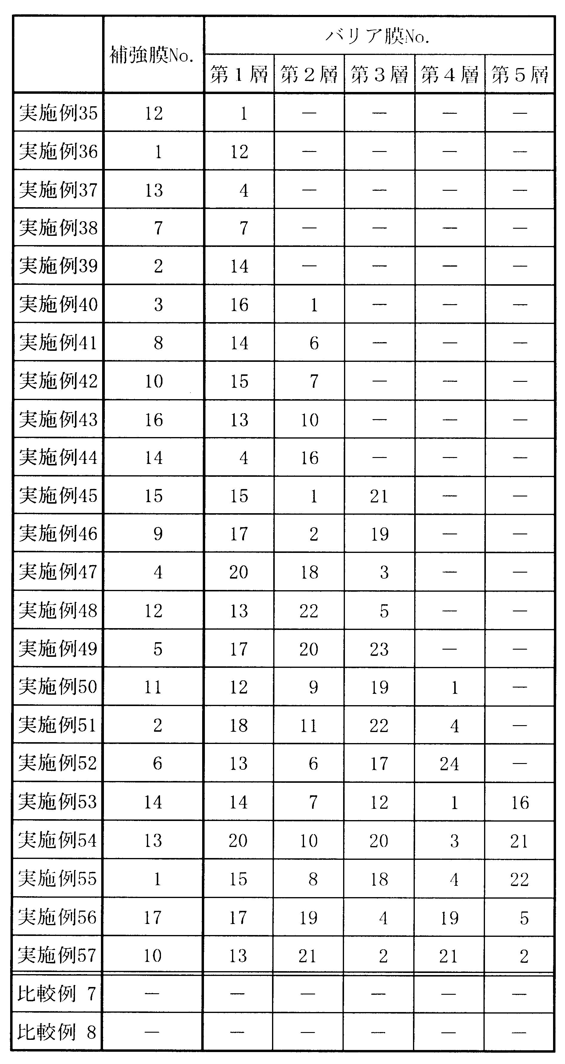
実施例35~57及び比較例7,8の太陽電池モジュールについて、以下の項目について評価を行った。これらの結果を以下の表11に示す。

先ず、図4に示すように、既に成膜が進んでいる太陽電池モジュールの光電変換ユニット13上にマグネトロンインライン式スパッタリング装置を用い、スパッタリング法により、厚さ80nmのZnO膜を形成し、これを透明導電膜14とした。次いで、上記表1の裏面電極層No.12による裏面電極層(銀電極層)16を形成した。次に、この裏面電極層16上に上記表2の補強膜No.12による補強膜17を形成した。次に、後述する光電変換ユニット13のパターニング位置(分離溝23)から50μm横の位置に、基板11側からレーザを照射してパターニングする。即ち、光電変換ユニット13、透明導電膜14、裏面電極層16及び裏面電極補強膜17を爆裂するレーザスクライブにより、補強膜17の表面から表面電極層12へ延びる分離溝18を形成することにより短冊状に分離加工した。レーザスクライブによる分離加工(分離溝18の形成)には、エネルギー密度0.7J/cm3、パルス周波数4kHzのNd:YAGレーザを用いた。最後に、分離溝18を埋めるとともに、補強膜17上に上記表3のバリア膜No.1による単一のバリア膜19を形成した。この太陽電池モジュールを実施例58とした。
次の表12に示すように、裏面電極層No.1により裏面電極層を形成し、補強膜No.1により補強膜を形成し、バリア膜No.12によりバリア膜を形成したこと以外は、実施例58と同様に太陽電池モジュールを形成した。
次の表12に示すように、裏面電極層No.13により裏面電極層を形成し、補強膜No.13により補強膜を形成し、バリア膜No.4によりバリア膜を形成したこと以外は、実施例58と同様に太陽電池モジュールを形成した。
次の表12に示すように、裏面電極層No.7により裏面電極層を形成し、補強膜No.7により補強膜を形成し、バリア膜No.7によりバリア膜を形成したこと以外は、実施例58と同様に太陽電池モジュールを形成した。
次の表12に示すように、裏面電極層No.2により裏面電極層を形成し、補強膜No.2により補強膜を形成し、バリア膜No.14によりバリア膜を形成したこと以外は、実施例58と同様に太陽電池モジュールを形成した。
次の表12に示すように、裏面電極層No.3により裏面電極層を形成し、補強膜No.3により補強膜を形成し、バリア膜No.16を成膜した後、更にバリア膜No.1を重ねて成膜して2層からなるバリア膜を形成したこと以外は、実施例58と同様に太陽電池モジュールを形成した。
次の表12に示すように、裏面電極層No.8により裏面電極層を形成し、補強膜No.8により補強膜を形成し、バリア膜No.14を成膜した後、更にバリア膜No.6を重ねて成膜して2層からなるバリア膜を形成したこと以外は、実施例58と同様に太陽電池モジュールを形成した。
次の表12に示すように、裏面電極層No.10により裏面電極層を形成し、補強膜No.10により補強膜を形成し、バリア膜No.15を成膜した後、更にバリア膜No.7を重ねて成膜して2層からなるバリア膜を形成したこと以外は、実施例58と同様に太陽電池モジュールを形成した。
次の表12に示すように、裏面電極層No.16により裏面電極層を形成し、補強膜No.16により補強膜を形成し、バリア膜No.13を成膜した後、更にバリア膜No.10を重ねて成膜して2層からなるバリア膜を形成したこと以外は、実施例58と同様に太陽電池モジュールを形成した。
次の表12に示すように、裏面電極層No.14により裏面電極層を形成し、補強膜No.14により補強膜を形成し、バリア膜No.4を成膜した後、更にバリア膜No.16を重ねて成膜して2層からなるバリア膜を形成したこと以外は、実施例58と同様に太陽電池モジュールを形成した。
次の表12に示すように、裏面電極層No.15により裏面電極層を形成し、補強膜No.15により補強膜を形成し、バリア膜No.15を成膜した後、バリア膜No.1を重ねて成膜し、更にバリア膜No.21を重ねて成膜して3層からなるバリア膜を形成したこと以外は、実施例58と同様に太陽電池モジュールを形成した。
次の表12に示すように、裏面電極層No.9により裏面電極層を形成し、補強膜No.9により補強膜を形成し、バリア膜No.17を成膜した後、バリア膜No.2を重ねて成膜し、更にバリア膜No.19を重ねて成膜して3層からなるバリア膜を形成したこと以外は、実施例58と同様に太陽電池モジュールを形成した。
次の表12に示すように、裏面電極層No.4により裏面電極層を形成し、補強膜No.4により補強膜を形成し、バリア膜No.20を成膜した後、バリア膜No.18を重ねて成膜し、更にバリア膜No.3を重ねて成膜して3層からなるバリア膜を形成したこと以外は、実施例58と同様に太陽電池モジュールを形成した。
次の表12に示すように、裏面電極層No.12により裏面電極層を形成し、補強膜No.12により補強膜を形成し、バリア膜No.13を成膜した後、バリア膜No.22を重ねて成膜し、更にバリア膜No.5を重ねて成膜して3層からなるバリア膜を形成したこと以外は、実施例58と同様に太陽電池モジュールを形成した。
次の表12に示すように、裏面電極層No.5により裏面電極層を形成し、補強膜No.5により補強膜を形成し、バリア膜No.17を成膜した後、バリア膜No.20を重ねて成膜し、更にバリア膜No.23を重ねて成膜して3層からなるバリア膜を形成したこと以外は、実施例58と同様に太陽電池モジュールを形成した。
次の表12に示すように、裏面電極層No.11により裏面電極層を形成し、補強膜No.11により補強膜を形成し、バリア膜No.12、No.9、No.19及びNo.1をこの順に重ねて成膜し、4層からなるバリア膜を形成したこと以外は、実施例58と同様に太陽電池モジュールを形成した。
次の表12に示すように、裏面電極層No.2により裏面電極層を形成し、補強膜No.2により補強膜を形成し、バリア膜No.18、No.11、No.22及びNo.4をこの順に重ねて成膜し、4層からなるバリア膜を形成したこと以外は、実施例58と同様に太陽電池モジュールを形成した。
次の表12に示すように、裏面電極層No.6により裏面電極層を形成し、補強膜No.6により補強膜を形成し、バリア膜No.13、No.6、No.17及びNo.24をこの順に重ねて成膜し、4層からなるバリア膜を形成したこと以外は、実施例58と同様に太陽電池モジュールを形成した。
次の表12に示すように、裏面電極層No.14により裏面電極層を形成し、補強膜No.14により補強膜を形成し、バリア膜No.14、No.7、No.12、No.1及びNo.16をこの順に重ねて成膜し、5層からなるバリア膜を形成したこと以外は、実施例58と同様に太陽電池モジュールを形成した。
次の表12に示すように、裏面電極層No.13により裏面電極層を形成し、補強膜No.13により補強膜を形成し、バリア膜No.20、No.10、No.20、No.3及びNo.21をこの順に重ねて成膜し、5層からなるバリア膜を形成したこと以外は、実施例58と同様に太陽電池モジュールを形成した。
次の表12に示すように、裏面電極層No.1により裏面電極層を形成し、補強膜No.1により補強膜を形成し、バリア膜No.15、No.8、No.18、No.4及びNo.22をこの順に重ねて成膜し、5層からなるバリア膜を形成したこと以外は、実施例58と同様に太陽電池モジュールを形成した。
次の表12に示すように、裏面電極層No.17により裏面電極層を形成し、補強膜No.17により補強膜を形成し、バリア膜No.17、No.19、No.4、No.19及びNo.5をこの順に重ねて成膜し、5層からなるバリア膜を形成したこと以外は、実施例58と同様に太陽電池モジュールを形成した。なお、この実施例では、発電層13は、絶縁性基板11側から順にp型a-Si(非晶質シリコン)、i型a-Si及びn型a-Siが積層した非晶質シリコン層1層からなる光電変換ユニットとした。
次の表12に示すように、裏面電極層No.10により裏面電極層を形成し、補強膜No.10により補強膜を形成し、バリア膜No.13、No.21、No.2、No.21及びNo.2をこの順に重ねて成膜し、5層からなるバリア膜を形成したこと以外は、実施例58と同様に太陽電池モジュールを形成した。なお、この実施例では、発電層13は、絶縁性基板11側から順にp型μc-Si(微結晶シリコン)、i型μc-Si及びn型μc-Siが積層した微結晶シリコン層1層からなる光電変換ユニットとした。
既に成膜が進んでいる太陽電池モジュールの裏面銀電極層を覆うように、厚さ15nmのチタン層を裏面銀電極補強膜として形成し、レーザ加工法によるスクライブ後、バリア材料としてEVA樹脂とPETフィルムをその上部に熱接着させて形成した。この太陽電池モジュールを比較例9とした。
既に成膜が進んでいる太陽電池モジュールの裏面銀電極層を覆うように、厚さ15nmのチタン層を裏面銀電極補強膜として形成し、レーザ加工法によるスクライブ後、バリア材料としてEVA樹脂とテドラーフィルム(デュポン社製)をその上部に熱接着させて形成した。この太陽電池モジュールを比較例10とした。

実施例58~80及び比較例9,10の太陽電池モジュールについて、以下の項目について評価を行った。これらの結果を以下の表13に示す。
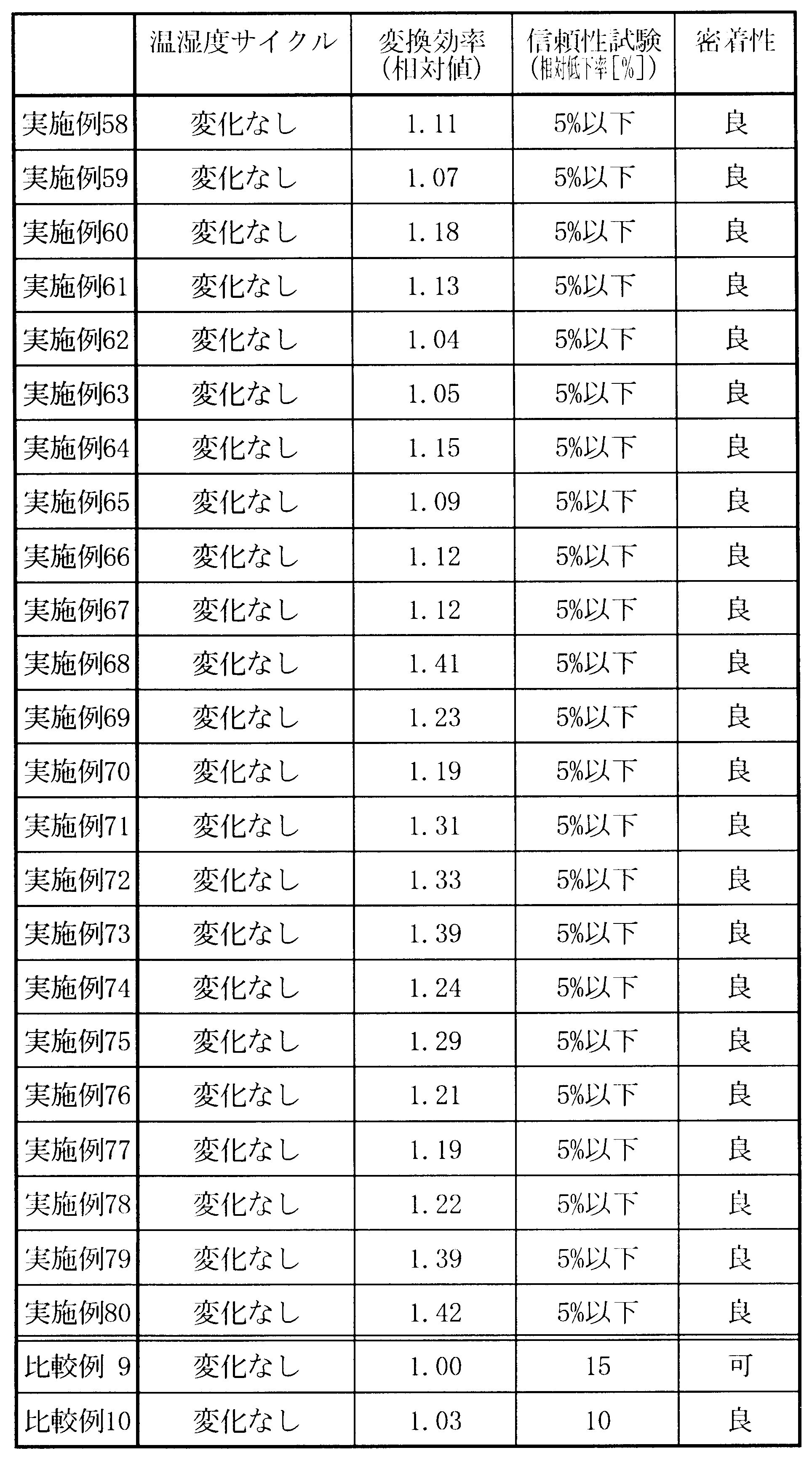
先ず、図4に示すように、既に成膜が進んでいる太陽電池モジュールの裏面電極層16(銀電極層)上に、スパッタ法により、裏面電極層(銀電極層)16を覆うように、厚さ15nmのチタン層を形成し、これを裏面電極層の補強膜17とした。次いで、後述する光電変換ユニット13のパターニング位置(分離溝23)から50μm横の位置に、基板11側からレーザを照射してパターニングする。即ち、光電変換ユニット13、透明導電膜14、裏面電極16および裏面電極補強膜17を爆裂するレーザスクライブにより、補強膜17の表面から表面電極層12へ延びる分離溝18を形成した。レーザスクライブによる分離加工(分離溝18の形成)には、エネルギー密度0.7J/cm3、パルス周波数4kHzのNd:YAGレーザを用いた。最後に、分離溝18を埋めるとともに、補強膜17上に上記表3のバリア膜No.1による単一のバリア膜を形成した。この太陽電池モジュールを実施例81とした。
次の表14に示すように、バリア膜No.12によりバリア膜を形成したこと以外は、実施例81と同様に太陽電池モジュールを形成した。
次の表14に示すように、バリア膜No.4によりバリア膜を形成したこと以外は、実施例81と同様に太陽電池モジュールを形成した。
次の表14に示すように、バリア膜No.7によりバリア膜を形成したこと以外は、実施例81と同様に太陽電池モジュールを形成した。
次の表14に示すように、バリア膜No.14によりバリア膜を形成したこと以外は、実施例81と同様に太陽電池モジュールを形成した。
次の表14に示すように、バリア膜No.16を成膜した後、更にバリア膜No.1を重ねて成膜して2層からなるバリア膜を形成したこと以外は、実施例81と同様に太陽電池モジュールを形成した。
次の表14に示すように、バリア膜No.14を成膜した後、更にバリア膜No.6を重ねて成膜して2層からなるバリア膜を形成したこと以外は、実施例81と同様に太陽電池モジュールを形成した。
次の表14に示すように、バリア膜No.15を成膜した後、更にバリア膜No.7を重ねて成膜して2層からなるバリア膜を形成したこと以外は、実施例81と同様に太陽電池モジュールを形成した。
次の表14に示すように、バリア膜No.13を成膜した後、更にバリア膜No.10を重ねて成膜して2層からなるバリア膜を形成したこと以外は、実施例81と同様に太陽電池モジュールを形成した。
次の表14に示すように、バリア膜No.4を成膜した後、更にバリア膜No.16を重ねて成膜して2層からなるバリア膜を形成したこと以外は、実施例81と同様に太陽電池モジュールを形成した。
次の表14に示すように、バリア膜No.15を成膜した後、バリア膜No.1を重ねて成膜し、更にバリア膜No.21を重ねて成膜して3層からなるバリア膜を形成したこと以外は、実施例81と同様に太陽電池モジュールを形成した。
次の表14に示すように、バリア膜No.17を成膜した後、バリア膜No.2を重ねて成膜し、更にバリア膜No.19を重ねて成膜して3層からなるバリア膜を形成したこと以外は、実施例81と同様に太陽電池モジュールを形成した。
次の表14に示すように、バリア膜No.20を成膜した後、バリア膜No.18を重ねて成膜し、更にバリア膜No.3を重ねて成膜して3層からなるバリア膜を形成したこと以外は、実施例81と同様に太陽電池モジュールを形成した。
次の表14に示すように、バリア膜No.13を成膜した後、バリア膜No.22を重ねて成膜し、更にバリア膜No.5を重ねて成膜して3層からなるバリア膜を形成したこと以外は、実施例81と同様に太陽電池モジュールを形成した。
次の表14に示すように、バリア膜No.17を成膜した後、バリア膜No.20を重ねて成膜し、更にバリア膜No.23を重ねて成膜して3層からなるバリア膜を形成したこと以外は、実施例81と同様に太陽電池モジュールを形成した。
次の表14に示すように、バリア膜No.12、バリア膜No.9、バリア膜No.19及びバリア膜No.1をこの順に重ねて成膜し、4層からなるバリア膜を形成したこと以外は、実施例81と同様に太陽電池モジュールを形成した。
次の表14に示すように、バリア膜No.18、バリア膜No.11、バリア膜No.22及びバリア膜No.4をこの順に重ねて成膜し、4層からなるバリア膜を形成したこと以外は、実施例81と同様に太陽電池モジュールを形成した。
次の表14に示すように、バリア膜No.13、バリア膜No.6、バリア膜No.17及びバリア膜No.24をこの順に重ねて成膜し、4層からなるバリア膜を形成したこと以外は、実施例81と同様に太陽電池モジュールを形成した。
次の表14に示すように、バリア膜No.14、バリア膜No.7、バリア膜No.12、バリア膜No.1及びバリア膜No.16をこの順に重ねて成膜し、5層からなるバリア膜を形成したこと以外は、実施例81と同様に太陽電池モジュールを形成した。
次の表14に示すように、バリア膜No.20、バリア膜No.10、バリア膜No.20、バリア膜No.3及びバリア膜No.21をこの順に重ねて成膜し、5層からなるバリア膜を形成したこと以外は、実施例81と同様に太陽電池モジュールを形成した。
次の表14に示すように、バリア膜No.15、バリア膜No.8、バリア膜No.18、バリア膜No.4及びバリア膜No.22をこの順に重ねて成膜し、5層からなるバリア膜を形成したこと以外は、実施例81と同様に太陽電池モジュールを形成した。
次の表14に示すように、バリア膜No.17、バリア膜No.19、バリア膜No.4、バリア膜No.19及びバリア膜No.5をこの順に重ねて成膜し、5層からなるバリア膜を形成したこと以外は、実施例81と同様に太陽電池モジュールを形成した。なお、この実施例では、発電層13は、基板11側から順にp型a-Si(非晶質シリコン)、i型a-Si及びn型a-Siが積層した非晶質シリコン層1層からなる光電変換ユニットとした。
次の表14に示すように、バリア膜No.13、バリア膜No.21、バリア膜No.2、バリア膜No.21及びバリア膜No.2をこの順に重ねて成膜し、5層からなるバリア膜を形成したこと以外は、実施例81と同様に太陽電池モジュールを形成した。なお、この実施例では、発電層13は、基板11側から順にp型μc-Si(微結晶シリコン)、i型μc-Si及びn型μc-Siが積層した微結晶シリコン層1層からなる光電変換ユニットとした。
既に成膜が進んでいる太陽電池モジュールの裏面銀電極層を覆うように、厚さ15nmのチタン層を裏面銀電極補強膜として形成し、レーザ加工法によるスクライブ後、バリア材料としてEVA樹脂とPETフィルムをその上部に熱接着させて形成した。この太陽電池モジュールを比較例11とした。
既に成膜が進んでいる太陽電池モジュールの裏面銀電極層を覆うように、厚さ15nmのチタン層を裏面銀電極補強膜として形成し、レーザ加工法によるスクライブ後、バリア材料としてEVA樹脂とテドラーフィルム(デュポン社製)をその上部に熱接着させて形成した。この太陽電池モジュールを比較例12とした。

実施例81~103及び比較例11,12の太陽電池モジュールについて、以下の項目について評価を行った。これらの結果を以下の表15に示す。
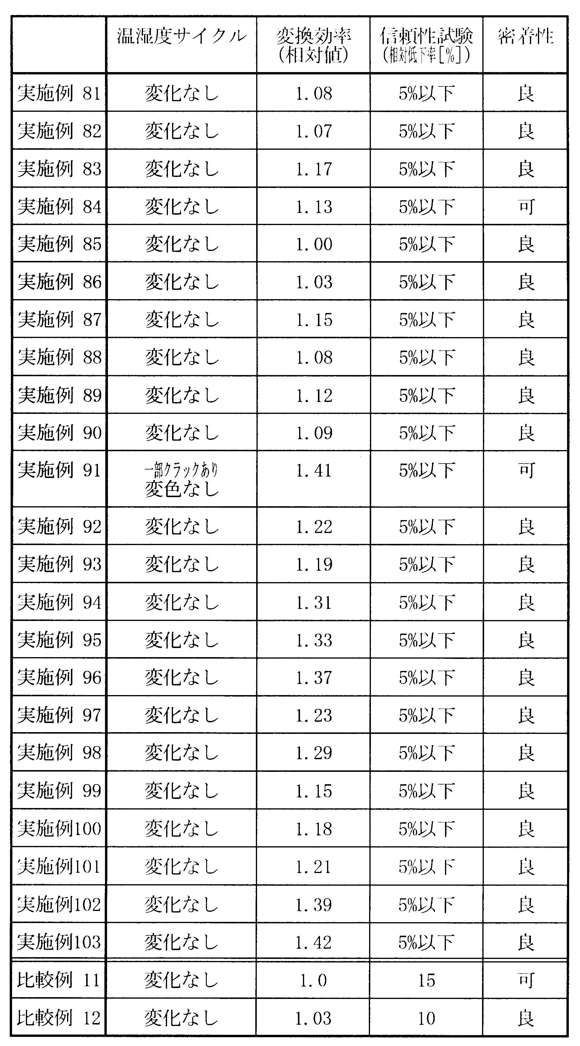
先ず、図4に示すように、既に成膜が進んでいる太陽電池モジュールの光電変換ユニット13上にマグネトロンインライン式スパッタリング装置を用い、スパッタリング法により、厚さ80nmのZnO膜を形成し、これを透明導電膜14とした。次いで、上記表1の裏面電極層No.12による裏面電極層(銀電極層)16を形成した。次に、この裏面電極層16上にマグネトロンインライン式スパッタリング装置を用い、スパッタリング法により、裏面電極層(銀電極層)16を覆うように、厚さ15nmのチタン層を形成し、これを裏面電極層の補強膜17とした。次に、後述する光電変換ユニット13のパターニング位置(分離溝23)から50μm横の位置に、基板11側からレーザを照射してパターニングする。即ち、光電変換ユニット13、透明導電膜14、裏面電極層16及び裏面電極補強膜17を爆裂するレーザスクライブにより、補強膜17の表面から表面電極層12へ延びる分離溝18を形成することにより短冊状に分離加工した。レーザスクライブによる分離加工(分離溝18の形成)には、エネルギー密度0.7J/cm3、パルス周波数4kHzのNd:YAGレーザを用いた。最後に、分離溝18を埋めるとともに、補強膜17上に上記表3のバリア膜No.1による単一のバリア膜19を形成した。この太陽電池モジュールを実施例104とした。
次の表16に示すように、裏面電極層No.1により裏面電極層を形成し、バリア膜No.12によりバリア膜を形成したこと以外は、実施例104と同様に太陽電池モジュールを形成した。
次の表16に示すように、裏面電極層No.13により裏面電極層を形成し、バリア膜No.4によりバリア膜を形成したこと以外は、実施例104と同様に太陽電池モジュールを形成した。
次の表16に示すように、裏面電極層No.7により裏面電極層を形成し、バリア膜No.7によりバリア膜を形成したこと以外は、実施例104と同様に太陽電池モジュールを形成した。
次の表16に示すように、裏面電極層No.2により裏面電極層を形成し、バリア膜No.14によりバリア膜を形成したこと以外は、実施例104と同様に太陽電池モジュールを形成した。
次の表16に示すように、裏面電極層No.3により裏面電極層を形成し、バリア膜No.16を成膜した後、更にバリア膜No.1を重ねて成膜して2層からなるバリア膜を形成したこと以外は、実施例104と同様に太陽電池モジュールを形成した。
次の表16に示すように、裏面電極層No.8により裏面電極層を形成し、バリア膜No.14を成膜した後、更にバリア膜No.6を重ねて成膜して2層からなるバリア膜を形成したこと以外は、実施例104と同様に太陽電池モジュールを形成した。
次の表16に示すように、裏面電極層No.10により裏面電極層を形成し、バリア膜No.15を成膜した後、更にバリア膜No.7を重ねて成膜して2層からなるバリア膜を形成したこと以外は、実施例104と同様に太陽電池モジュールを形成した。
次の表16に示すように、裏面電極層No.16により裏面電極層を形成し、バリア膜No.13を成膜した後、更にバリア膜No.10を重ねて成膜して2層からなるバリア膜を形成したこと以外は、実施例104と同様に太陽電池モジュールを形成した。
次の表16に示すように、裏面電極層No.14により裏面電極層を形成し、バリア膜No.4を成膜した後、更にバリア膜No.16を重ねて成膜して2層からなるバリア膜を形成したこと以外は、実施例104と同様に太陽電池モジュールを形成した。
次の表16に示すように、裏面電極層No.15により裏面電極層を形成し、バリア膜No.15を成膜した後、バリア膜No.1を重ねて成膜し、更にバリア膜No.21を重ねて成膜して3層からなるバリア膜を形成したこと以外は、実施例104と同様に太陽電池モジュールを形成した。
次の表16に示すように、裏面電極層No.9により裏面電極層を形成し、バリア膜No.17を成膜した後、バリア膜No.2を重ねて成膜し、更にバリア膜No.19を重ねて成膜して3層からなるバリア膜を形成したこと以外は、実施例104と同様に太陽電池モジュールを形成した。
次の表16に示すように、裏面電極層No.4により裏面電極層を形成し、バリア膜No.20を成膜した後、バリア膜No.18を重ねて成膜し、更にバリア膜No.3を重ねて成膜して3層からなるバリア膜を形成したこと以外は、実施例104と同様に太陽電池モジュールを形成した。
次の表16に示すように、裏面電極層No.12により裏面電極層を形成し、バリア膜No.13を成膜した後、バリア膜No.22を重ねて成膜し、更にバリア膜No.5を重ねて成膜して3層からなるバリア膜を形成したこと以外は、実施例104と同様に太陽電池モジュールを形成した。
次の表16に示すように、裏面電極層No.5により裏面電極層を形成し、バリア膜No.17を成膜した後、バリア膜No.20を重ねて成膜し、更にバリア膜No.23を重ねて成膜して3層からなるバリア膜を形成したこと以外は、実施例104と同様に太陽電池モジュールを形成した。
次の表16に示すように、裏面電極層No.11により裏面電極層を形成し、バリア膜No.12、No.9、No.19及びNo.1をこの順に重ねて成膜し、4層からなるバリア膜を形成したこと以外は、実施例104と同様に太陽電池モジュールを形成した。
次の表16に示すように、裏面電極層No.2により裏面電極層を形成し、バリア膜No.18、No.11、No.22及びNo.4をこの順に重ねて成膜し、4層からなるバリア膜を形成したこと以外は、実施例104と同様に太陽電池モジュールを形成した。
次の表16に示すように、裏面電極層No.6により裏面電極層を形成し、バリア膜No.13、No.6、No.17及びNo.24をこの順に重ねて成膜し、4層からなるバリア膜を形成したこと以外は、実施例104と同様に太陽電池モジュールを形成した。
次の表16に示すように、裏面電極層No.14により裏面電極層を形成し、バリア膜No.14、No.7、No.12、No.1及びNo.16をこの順に重ねて成膜し、5層からなるバリア膜を形成したこと以外は、実施例104と同様に太陽電池モジュールを形成した。
次の表16に示すように、裏面電極層No.13により裏面電極層を形成し、バリア膜No.20、No.10、No.20、No.3及びNo.21をこの順に重ねて成膜し、5層からなるバリア膜を形成したこと以外は、実施例104と同様に太陽電池モジュールを形成した。
次の表16に示すように、裏面電極層No.1により裏面電極層を形成し、バリア膜No.15、No.8、No.18、No.4及びNo.22をこの順に重ねて成膜し、5層からなるバリア膜を形成したこと以外は、実施例104と同様に太陽電池モジュールを形成した。
次の表16に示すように、裏面電極層No.17により裏面電極層を形成し、バリア膜No.17、No.19、No.4、No.19及びNo.5をこの順に重ねて成膜し、5層からなるバリア膜を形成したこと以外は、実施例104と同様に太陽電池モジュールを形成した。なお、この実施例では、発電層13は、絶縁性基板11側から順にp型a-Si(非晶質シリコン)、i型a-Si及びn型a-Siが積層した非晶質シリコン層1層からなる光電変換ユニットとした。
次の表16に示すように、裏面電極層No.10により裏面電極層を形成し、バリア膜No.13、No.21、No.2、No.21及びNo.2をこの順に重ねて成膜し、5層からなるバリア膜を形成したこと以外は、実施例104と同様に太陽電池モジュールを形成した。なお、この実施例では、発電層13は、絶縁性基板11側から順にp型μc-Si(微結晶シリコン)、i型μc-Si及びn型μc-Siが積層した微結晶シリコン層1層からなる光電変換ユニットとした。
既に成膜が進んでいる太陽電池モジュールの裏面銀電極層を覆うように、厚さ15nmのチタン層を裏面銀電極補強膜として形成し、レーザ加工法によるスクライブ後、バリア材料としてEVA樹脂とPETフィルムをその上部に熱接着させて形成した。この太陽電池モジュールを比較例13とした。
既に成膜が進んでいる太陽電池モジュールの裏面銀電極層を覆うように、厚さ15nmのチタン層を裏面銀電極補強膜として形成し、レーザ加工法によるスクライブ後、バリア材料としてEVA樹脂とテドラーフィルム(デュポン社製)をその上部に熱接着させて形成した。この太陽電池モジュールを比較例14とした。

実施例104~126及び比較例13,14の太陽電池モジュールについて、以下の項目について評価を行った。これらの結果を以下の表17に示す。
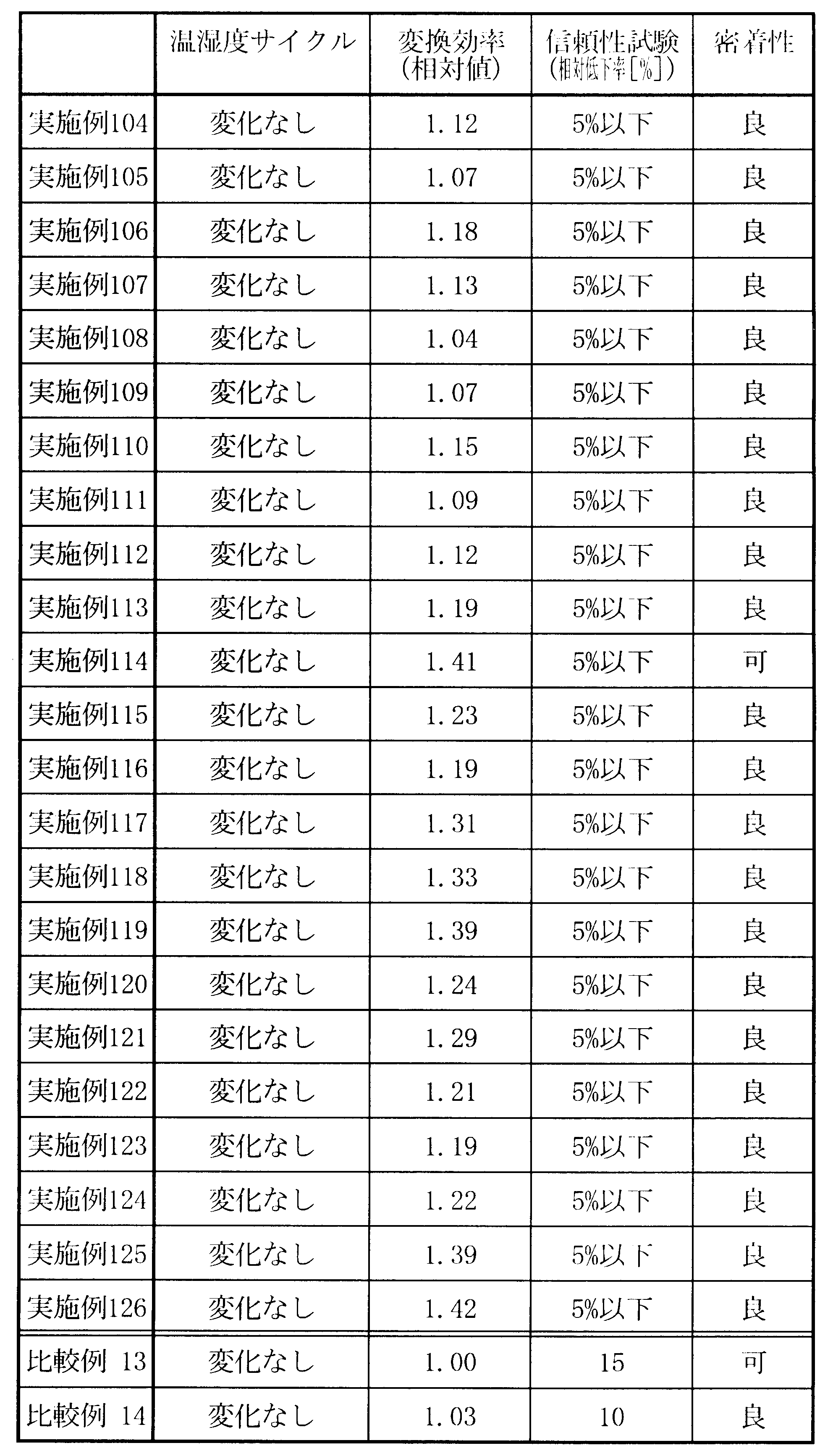
11 基板
12 表面電極層
13,53 光電変換ユニット
14 透明導電膜
15,55 光起電力素子
16 裏面電極層
17 裏面電極補強膜
19 充填剤層
24 バリア膜
Claims (25)
- 基板上に透明で導電性を有する表面電極層を形成する工程と、
前記表面電極層上に光により発電する光電変換ユニットを1又は2以上形成する工程と、
前記光電変換ユニット上に透明導電膜を形成する工程と、
前記透明導電膜上に裏面電極層を形成する工程と、
前記裏面電極層上に補強膜用組成物を湿式塗工法により塗布して得られた層に紫外線照射するか又は加熱するか或いは紫外線照射した後に加熱して裏面電極補強膜を形成する工程と
を含む太陽電池モジュールの製造方法。 - 光電変換ユニットが、非晶質シリコン層又は微結晶シリコン層のいずれか一方を1層又は2層以上含むか、或いは前記非晶質シリコン層及び前記微結晶シリコン層を1層ずつ以上含む請求項1記載の太陽電池モジュールの製造方法。
- 補強膜用組成物が、紫外線照射するか又は加熱するか或いは紫外線照射した後に加熱することにより硬化するポリマー型バインダの有機系又は無機系ベース材料或いはノンポリマー型バインダの無機系ベース材料のいずれか一方又は双方を含む請求項1記載の太陽電池モジュールの製造方法。
- 前記裏面電極補強膜を形成する工程の後に、前記補強膜上にバリア膜用組成物を湿式塗工法により塗布して得られた層に紫外線照射するか又は加熱するか或いは紫外線照射した後に加熱してバリア膜を形成する工程を更に含む請求項1記載の太陽電池モジュールの製造方法。
- バリア膜用組成物が、紫外線照射するか又は加熱するか或いは紫外線照射した後に加熱することにより硬化するポリマー型バインダの有機系又は無機系ベース材料或いはノンポリマー型バインダの無機系ベース材料のいずれか一方又は双方を含む請求項4記載の太陽電池モジュールの製造方法。
- バリア膜がポリマー型バインダの無機系ベース材料又はノンポリマー型バインダの無機系ベース材料を含有するバリア膜用組成物を用いた1又は2以上の無機系バリア膜と、ポリマー型の有機系ベース材料を含有するバリア膜用組成物を用いた1又は2以上の有機系バリア膜を交互に重ねて形成される請求項4記載の太陽電池モジュールの製造方法。
- 補強膜用組成物が、コロイダルシリカ、フュームドシリカ粒子、シリカ粒子、マイカ粒子及びスメクタイト粒子からなる群より選ばれた1種又は2種以上の金属酸化物微粒子又は扁平粒子を含む請求項1記載の太陽電池モジュールの製造方法。
- バリア膜用組成物が、コロイダルシリカ、フュームドシリカ粒子、シリカ粒子、マイカ粒子及びスメクタイト粒子からなる群より選ばれた1種又は2種以上の金属酸化物微粒子又は扁平粒子を含む請求項4記載の太陽電池モジュールの製造方法。
- 補強膜用組成物が、金、白金、パラジウム、ルテニウム、ニッケル、銅、錫、インジウム、亜鉛、鉄、クロム、マンガン及びアルミニウムからなる群より選ばれた1種又は2種以上の金属又はこれらの金属酸化物を含有する微粒子又は扁平微粒子を含み、前記金属又は前記金属酸化物の前記微粒子又は前記扁平微粒子中における含有量が70質量%以上である請求項1記載の太陽電池モジュールの製造方法。
- バリア膜用組成物が、金、白金、パラジウム、ルテニウム、ニッケル、銅、錫、インジウム、亜鉛、鉄、クロム、マンガン及びアルミニウムからなる群より選ばれた1種又は2種以上の金属又はこれらの金属酸化物を含有する微粒子又は扁平微粒子を含み、前記金属又は前記金属酸化物の前記微粒子又は前記扁平微粒子中における含有量が70質量%以上である請求項4記載の太陽電池モジュールの製造方法。
- 前記裏面電極層が、前記透明導電膜上に銀を含む電極用組成物を湿式塗工法により塗布して得られた層を加熱することにより形成される請求項1記載の太陽電池モジュールの製造方法。
- 裏面電極補強膜の厚さが裏面電極層の厚さの0.2~1倍である請求項1記載の太陽電池モジュールの製造方法。
- 透明導電膜の厚さが0.03~0.5μmの範囲内であり、
裏面電極層の厚さが0.05~2.0μmの範囲内であり、
補強膜用組成物に紫外線照射するか又は120~400℃に加熱するか或いは紫外線照射した後に120~400℃に加熱して形成された裏面電極補強膜の厚さが0.01~2.0μmの範囲内である
請求項1記載の太陽電池モジュールの製造方法。 - バリア膜用組成物に紫外線照射するか又は120~400℃に加熱するか或いは紫外線照射した後に120~400℃に加熱して形成されたバリア膜の厚さが0.2~20μmの範囲内である
請求項4記載の太陽電池モジュールの製造方法。 - 基板上に形成された表面電極層、光電変換ユニット、透明電極層及び裏面電極層により光起電力素子が構成され、前記光起電力素子が前記基板上に隙間をあけて複数配設され、前記複数の光起電力素子が電気的に直列に接続され、更に前記隙間に充填剤層が配置された請求項1記載の太陽電池モジュールの製造方法。
- 基板上に形成された表面電極層、光電変換ユニット、透明電極層及び裏面電極層により光起電力素子が構成され、前記光起電力素子が前記基板上に隙間をあけて複数配設され、前記複数の光起電力素子が電気的に直列に接続され、更に前記隙間にバリア膜が配置された請求項4記載の太陽電池モジュールの製造方法。
- 基板上に透明で導電性を有する表面電極層を形成する工程と、
前記表面電極層上に光により発電する光電変換ユニットを1又は2以上形成する工程と、
前記光電変換ユニット上に透明導電膜を形成する工程と、
前記透明導電膜上に裏面電極層を形成する工程と、
前記裏面電極層上にバリア膜用組成物を湿式塗工法により塗布して得られた層に紫外線照射するか又は加熱するか或いは紫外線照射した後に加熱してバリア膜を形成する工程と
を含む太陽電池モジュールの製造方法。 - 光電変換ユニットが、非晶質シリコン層又は微結晶シリコン層のいずれか一方を1層又は2層以上含むか、或いは前記非晶質シリコン層及び前記微結晶シリコン層の双方を1層ずつ以上含む請求項17記載の太陽電池モジュールの製造方法。
- バリア膜用組成物が、紫外線照射するか又は加熱するか或いは紫外線照射した後に加熱することにより硬化するポリマー型バインダの有機系又は無機系ベース材料或いはノンポリマー型バインダの無機系ベース材料のいずれか一方又は双方を含む請求項17記載の太陽電池モジュールの製造方法。
- バリア膜がポリマー型バインダの無機系ベース材料又はノンポリマー型バインダの無機系ベース材料を含有するバリア膜用組成物を用いた1又は2以上の無機系バリア膜と、ポリマー型の有機系ベース材料を含有するバリア膜用組成物を用いた1又は2以上の有機系バリア膜を交互に重ねて形成される請求項17記載の太陽電池モジュールの製造方法。
- バリア膜用組成物が、コロイダルシリカ、フュームドシリカ粒子、シリカ粒子、マイカ粒子及びスメクタイト粒子からなる群より選ばれた1種又は2種以上の金属酸化物微粒子又は扁平粒子を含む請求項17記載の太陽電池モジュールの製造方法。
- バリア膜用組成物が、金、白金、パラジウム、ルテニウム、ニッケル、銅、錫、インジウム、亜鉛、鉄、クロム、マンガン及びアルミニウムからなる群より選ばれた1種又は2種以上の金属又はこれらの金属酸化物を含有する微粒子又は扁平微粒子を含み、前記金属又は前記金属酸化物の前記微粒子又は前記扁平微粒子中における含有量が70質量%以上である請求項17記載の太陽電池モジュールの製造方法。
- 前記裏面電極層が、前記透明導電膜上に銀を含む電極用組成物を湿式塗工法により塗布して得られた層を加熱することにより形成される請求項17記載の太陽電池モジュールの製造方法。
- 透明導電膜の厚さが0.03~0.5μmの範囲内であり、
裏面電極層の厚さが0.05~2.0μmの範囲内であり、
バリア膜用組成物に紫外線照射するか又は120~400℃に加熱するか或いは紫外線照射した後に120~400℃に加熱して形成されたバリア膜の厚さが0.2~20μmの範囲内である
請求項17記載の太陽電池モジュールの製造方法。 - 基板上に形成された表面電極層、光電変換ユニット、透明電極層及び裏面電極層により光起電力素子が構成され、前記光起電力素子が前記基板上に隙間をあけて複数配設され、前記複数の光起電力素子が電気的に直列に接続され、更に前記隙間にバリア膜が配置された請求項17記載の太陽電池モジュールの製造方法。
Priority Applications (3)
| Application Number | Priority Date | Filing Date | Title |
|---|---|---|---|
| JP2011507111A JPWO2010113708A1 (ja) | 2009-03-30 | 2010-03-24 | 太陽電池モジュールの製造方法 |
| CN2010800128537A CN102362357A (zh) | 2009-03-30 | 2010-03-24 | 太阳能电池模块的制造方法 |
| US13/138,747 US20120015472A1 (en) | 2009-03-30 | 2010-03-24 | Method of producing solar cell module |
Applications Claiming Priority (12)
| Application Number | Priority Date | Filing Date | Title |
|---|---|---|---|
| JP2009082057 | 2009-03-30 | ||
| JP2009-082057 | 2009-03-30 | ||
| JP2009-082075 | 2009-03-30 | ||
| JP2009-082130 | 2009-03-30 | ||
| JP2009082027 | 2009-03-30 | ||
| JP2009082111 | 2009-03-30 | ||
| JP2009-082038 | 2009-03-30 | ||
| JP2009082130 | 2009-03-30 | ||
| JP2009082038 | 2009-03-30 | ||
| JP2009082075 | 2009-03-30 | ||
| JP2009-082027 | 2009-03-30 | ||
| JP2009-082111 | 2009-03-30 |
Publications (1)
| Publication Number | Publication Date |
|---|---|
| WO2010113708A1 true WO2010113708A1 (ja) | 2010-10-07 |
Family
ID=42828003
Family Applications (1)
| Application Number | Title | Priority Date | Filing Date |
|---|---|---|---|
| PCT/JP2010/055013 Ceased WO2010113708A1 (ja) | 2009-03-30 | 2010-03-24 | 太陽電池モジュールの製造方法 |
Country Status (4)
| Country | Link |
|---|---|
| US (1) | US20120015472A1 (ja) |
| JP (2) | JPWO2010113708A1 (ja) |
| CN (1) | CN102362357A (ja) |
| WO (1) | WO2010113708A1 (ja) |
Cited By (9)
| Publication number | Priority date | Publication date | Assignee | Title |
|---|---|---|---|---|
| WO2012063908A1 (ja) * | 2010-11-12 | 2012-05-18 | 三菱マテリアル株式会社 | 発光素子向け反射膜用組成物、発光素子、および発光素子の製造方法 |
| WO2012104421A1 (de) | 2011-02-04 | 2012-08-09 | Azur Space Solar Power Gmbh | Mehrfachsolarzelle sowie verfahren zur herstellung einer solchen |
| WO2012110195A1 (de) * | 2011-02-14 | 2012-08-23 | Li-Tec Battery Gmbh | Verfahren zur herstellung von elektroden |
| JP2012191189A (ja) * | 2011-02-21 | 2012-10-04 | Semiconductor Energy Lab Co Ltd | 光電変換装置 |
| CN103258864A (zh) * | 2012-02-20 | 2013-08-21 | 三菱综合材料株式会社 | 导电性反射膜及其制造方法 |
| US8894888B2 (en) * | 2011-12-21 | 2014-11-25 | E I Du Pont De Nemours And Company | Conductive paste composition with synthetic clay additive and its use in the manufacture of semiconductor devices |
| US9437767B2 (en) | 2011-02-04 | 2016-09-06 | Azur Space Solar Power Gmbh | Multiple solar cell and method for manufacturing the same |
| KR101783784B1 (ko) | 2011-11-29 | 2017-10-11 | 한국전자통신연구원 | 태양전지 모듈 및 그의 제조방법 |
| JP2018127553A (ja) * | 2017-02-09 | 2018-08-16 | 協立化学産業株式会社 | 高い平滑性とパターン精度で塗工できる塗液 |
Families Citing this family (20)
| Publication number | Priority date | Publication date | Assignee | Title |
|---|---|---|---|---|
| DE112009002056T5 (de) * | 2008-08-27 | 2011-07-14 | Mitsubishi Materials Corporation | Transparenter elektrisch leitfähiger Film für Solarzellen, Zusammensetzung für transparente elektrisch leitfähige Filme und Mehrfach-Solarzellen |
| FR2978301B1 (fr) * | 2011-07-18 | 2013-08-02 | Renault Sa | Procede d'assemblage d'un transducteur ultrasonore et transducteur obtenu par le procede |
| JP2015523707A (ja) | 2012-04-18 | 2015-08-13 | ヘレウス プレシャス メタルズ ノース アメリカ コンショホーケン エルエルシー | 太陽電池接点の印刷方法 |
| FR2990300B1 (fr) * | 2012-05-04 | 2017-02-03 | Disasolar | Module photovoltaique et son procede de realisation. |
| TWI462314B (zh) * | 2012-05-17 | 2014-11-21 | Univ Minghsin Sci & Tech | 薄膜太陽能電池及其製造方法 |
| KR102007864B1 (ko) * | 2016-10-31 | 2019-08-07 | 엘에스니꼬동제련 주식회사 | 태양전지 전극용 도전성 페이스트 및 이를 사용하여 제조된 태양전지 |
| MY190562A (en) | 2016-12-20 | 2022-04-27 | Zhejiang Kaiying New Mat Co Ltd | Interdigitated back contact metal-insulator-semiconductor solar cell with printed oxide tunnel junctions |
| MY189222A (en) * | 2016-12-20 | 2022-01-31 | Zhejiang Kaiying New Mat Co Ltd | Siloxane-containing solar cell metallization pastes |
| WO2020021982A1 (ja) * | 2018-07-24 | 2020-01-30 | シャープ株式会社 | 太陽電池ユニットおよび太陽電池ユニットを備えた無線発信機 |
| US11329177B2 (en) * | 2018-11-08 | 2022-05-10 | Swift Solar Inc | Stable perovskite module interconnects |
| US10749045B1 (en) | 2019-05-23 | 2020-08-18 | Zhejiang Kaiying New Materials Co., Ltd. | Solar cell side surface interconnects |
| US10622502B1 (en) | 2019-05-23 | 2020-04-14 | Zhejiang Kaiying New Materials Co., Ltd. | Solar cell edge interconnects |
| CN112652721B (zh) * | 2020-12-22 | 2022-11-01 | 中国科学院长春应用化学研究所 | 低电阻高透过率低粗糙度的银纳米线复合电极及其制备方法和应用 |
| US12094663B2 (en) | 2021-09-30 | 2024-09-17 | Swift Solar Inc. | Bypass diode interconnect for thin film solar modules |
| CN114014972B (zh) * | 2021-11-15 | 2022-11-08 | 上海银浆科技有限公司 | 一种光伏银浆中有机载体用的酮肼交联体系 |
| US20250040288A1 (en) * | 2021-12-08 | 2025-01-30 | Lumileds Llc | Monolithic Optical Transformer |
| JP2025533330A (ja) * | 2022-09-28 | 2025-10-06 | ネクスティーシー・コーポレーション | 透明導電酸化物層の溶液ベースの平滑化 |
| KR20250131768A (ko) * | 2022-11-04 | 2025-09-03 | 케일룩스 코포레이션 | 캡슐화된 페로브스카이트 모듈 및 이를 포함하는 태양 전지 |
| US12154727B2 (en) | 2022-12-22 | 2024-11-26 | Swift Solar Inc. | Integrated bypass diode schemes for solar modules |
| CN116313905B (zh) * | 2023-02-16 | 2026-02-03 | 中芯越州集成电路制造(绍兴)有限公司 | 避免解键合印记的方法及功率器件的制备方法 |
Citations (4)
| Publication number | Priority date | Publication date | Assignee | Title |
|---|---|---|---|---|
| JPH02749U (ja) * | 1987-10-30 | 1990-01-05 | ||
| JP2001053305A (ja) * | 1999-08-12 | 2001-02-23 | Kanegafuchi Chem Ind Co Ltd | 非単結晶シリコン系薄膜光電変換装置 |
| JP2001217441A (ja) * | 2000-02-04 | 2001-08-10 | Dainippon Printing Co Ltd | 太陽電池モジュ−ル |
| JP2008140920A (ja) * | 2006-11-30 | 2008-06-19 | Sanyo Electric Co Ltd | 太陽電池モジュール及び太陽電池モジュールの製造方法 |
Family Cites Families (17)
| Publication number | Priority date | Publication date | Assignee | Title |
|---|---|---|---|---|
| JPS6055066A (ja) * | 1983-09-06 | 1985-03-29 | Mitsubishi Electric Corp | エポキシ粉体塗料 |
| JPS62212475A (ja) * | 1986-03-12 | 1987-09-18 | Yashima:Kk | 鉄板屋根の防食塗料 |
| JP2748471B2 (ja) * | 1988-12-22 | 1998-05-06 | 株式会社村田製作所 | 非晶質太陽電池 |
| JP3268893B2 (ja) * | 1993-06-29 | 2002-03-25 | キヤノン株式会社 | 光起電力素子の製造方法 |
| US5427853A (en) * | 1993-12-20 | 1995-06-27 | General Motors Corporation | Reinforcement preform, method of making same and reinforced composite made therefrom |
| JP3387741B2 (ja) * | 1995-07-19 | 2003-03-17 | キヤノン株式会社 | 半導体素子用保護材、該保護材を有する半導体素子、該素子を有する半導体装置 |
| DE60044384D1 (de) * | 1999-02-25 | 2010-06-24 | Kaneka Corp | Photoelektrische Dünnschicht-Umwandlungsvorrichtung und Verfahren zur Abscheidung durch Zerstäubung |
| KR20010009582A (ko) * | 1999-07-12 | 2001-02-05 | 최동환 | 저밀도 고강도의 단열재 및 그 제조방법 |
| JP2001290135A (ja) * | 2000-01-31 | 2001-10-19 | Nitto Denko Corp | タッチ式液晶表示装置及び入力検出方法 |
| JP2003031830A (ja) * | 2001-07-12 | 2003-01-31 | Sanyo Electric Co Ltd | 光起電力装置及び光起電力装置の製造方法 |
| US20030236318A1 (en) * | 2002-04-18 | 2003-12-25 | Kuraray Co., Ltd. | Curable resin composition, method for manufacture of laminate using the composition, transfer material, method for manufacture thereof and transferred product |
| JP4779074B2 (ja) * | 2003-10-03 | 2011-09-21 | 三井・デュポンポリケミカル株式会社 | 太陽電池封止材用シート |
| JP4929625B2 (ja) * | 2004-10-28 | 2012-05-09 | Jsr株式会社 | 硬化性組成物、その硬化層及び積層体 |
| JP2006152125A (ja) * | 2004-11-29 | 2006-06-15 | Sumitomo Metal Mining Co Ltd | 耐食光輝性顔料、その製造方法、および耐食光輝性塗膜用塗料組成物 |
| EP2190027B1 (en) * | 2007-09-12 | 2016-04-13 | Mitsubishi Materials Corporation | Process for producing a composite membrane for superstrate solar cell |
| US8153249B2 (en) * | 2008-08-26 | 2012-04-10 | Snu R&Db Foundation | Article treated with silica particles and method for treating a surface of the article |
| JP2010192377A (ja) * | 2009-02-20 | 2010-09-02 | Jsr Corp | フラットパネルディスプレイ部材形成用組成物 |
-
2010
- 2010-03-24 JP JP2011507111A patent/JPWO2010113708A1/ja active Pending
- 2010-03-24 WO PCT/JP2010/055013 patent/WO2010113708A1/ja not_active Ceased
- 2010-03-24 CN CN2010800128537A patent/CN102362357A/zh active Pending
- 2010-03-24 US US13/138,747 patent/US20120015472A1/en not_active Abandoned
-
2013
- 2013-04-09 JP JP2013081260A patent/JP2013189637A/ja active Pending
Patent Citations (4)
| Publication number | Priority date | Publication date | Assignee | Title |
|---|---|---|---|---|
| JPH02749U (ja) * | 1987-10-30 | 1990-01-05 | ||
| JP2001053305A (ja) * | 1999-08-12 | 2001-02-23 | Kanegafuchi Chem Ind Co Ltd | 非単結晶シリコン系薄膜光電変換装置 |
| JP2001217441A (ja) * | 2000-02-04 | 2001-08-10 | Dainippon Printing Co Ltd | 太陽電池モジュ−ル |
| JP2008140920A (ja) * | 2006-11-30 | 2008-06-19 | Sanyo Electric Co Ltd | 太陽電池モジュール及び太陽電池モジュールの製造方法 |
Cited By (18)
| Publication number | Priority date | Publication date | Assignee | Title |
|---|---|---|---|---|
| CN103180980B (zh) * | 2010-11-12 | 2017-04-26 | 三菱综合材料株式会社 | 使用反射膜用组合物的发光元件及其制造方法 |
| CN103180980A (zh) * | 2010-11-12 | 2013-06-26 | 三菱综合材料株式会社 | 用于发光元件的反射膜用组合物、发光元件及发光元件的制造方法 |
| WO2012063908A1 (ja) * | 2010-11-12 | 2012-05-18 | 三菱マテリアル株式会社 | 発光素子向け反射膜用組成物、発光素子、および発光素子の製造方法 |
| US9647185B2 (en) | 2010-11-12 | 2017-05-09 | Mitsubishi Materials Corporation | Composition for reflection film for light emitting element, light emitting element, and method of producing light emitting element |
| JP5998481B2 (ja) * | 2010-11-12 | 2016-09-28 | 三菱マテリアル株式会社 | 発光素子の製造方法 |
| WO2012104421A1 (de) | 2011-02-04 | 2012-08-09 | Azur Space Solar Power Gmbh | Mehrfachsolarzelle sowie verfahren zur herstellung einer solchen |
| CN103403874B (zh) * | 2011-02-04 | 2017-07-18 | 阿祖尔太空太阳能有限责任公司 | 多重太阳能电池及其制造方法 |
| CN103403874A (zh) * | 2011-02-04 | 2013-11-20 | 阿祖尔太空太阳能有限责任公司 | 多重太阳能电池及其制造方法 |
| US9437767B2 (en) | 2011-02-04 | 2016-09-06 | Azur Space Solar Power Gmbh | Multiple solar cell and method for manufacturing the same |
| WO2012110195A1 (de) * | 2011-02-14 | 2012-08-23 | Li-Tec Battery Gmbh | Verfahren zur herstellung von elektroden |
| JP2012191189A (ja) * | 2011-02-21 | 2012-10-04 | Semiconductor Energy Lab Co Ltd | 光電変換装置 |
| KR101783784B1 (ko) | 2011-11-29 | 2017-10-11 | 한국전자통신연구원 | 태양전지 모듈 및 그의 제조방법 |
| US8894888B2 (en) * | 2011-12-21 | 2014-11-25 | E I Du Pont De Nemours And Company | Conductive paste composition with synthetic clay additive and its use in the manufacture of semiconductor devices |
| TWI563520B (en) * | 2012-02-20 | 2016-12-21 | Mitsubishi Materials Corp | Production method of reflector film with electrical conductivity |
| US9281421B2 (en) | 2012-02-20 | 2016-03-08 | Mitsubishi Materials Corporation | Conductive reflective film and method of manufacturing the same |
| JP2013171893A (ja) * | 2012-02-20 | 2013-09-02 | Mitsubishi Materials Corp | 導電性反射膜およびその製造方法 |
| CN103258864A (zh) * | 2012-02-20 | 2013-08-21 | 三菱综合材料株式会社 | 导电性反射膜及其制造方法 |
| JP2018127553A (ja) * | 2017-02-09 | 2018-08-16 | 協立化学産業株式会社 | 高い平滑性とパターン精度で塗工できる塗液 |
Also Published As
| Publication number | Publication date |
|---|---|
| US20120015472A1 (en) | 2012-01-19 |
| CN102362357A (zh) | 2012-02-22 |
| JPWO2010113708A1 (ja) | 2012-10-11 |
| JP2013189637A (ja) | 2013-09-26 |
Similar Documents
| Publication | Publication Date | Title |
|---|---|---|
| WO2010113708A1 (ja) | 太陽電池モジュールの製造方法 | |
| CN105513670A (zh) | 太阳能电池用透明导电膜及其透明导电膜用组合物、多接合型太阳能电池 | |
| JP5637196B2 (ja) | スーパーストレート型薄膜太陽電池用の複合膜及びその製造方法 | |
| CN102201274A (zh) | 导电膜形成用组成物、太阳能电池用复合膜及其形成方法 | |
| JP5544774B2 (ja) | 多接合型太陽電池 | |
| JP2011222953A (ja) | 透明導電膜形成用組成物及び太陽電池用の複合膜の形成方法並びに該方法により形成された複合膜 | |
| JP2010087479A (ja) | サブストレート型太陽電池用の複合膜及びその製造方法 | |
| JP2010087478A (ja) | スーパーストレート型太陽電池用の複合膜及びその製造方法 | |
| WO2010023920A1 (ja) | 太陽電池用透明導電膜及びその透明導電膜用組成物、多接合型太陽電池 | |
| TWI593123B (zh) | 薄膜太陽能電池用層合體、及使用此之薄膜太陽能電池之製造方法 | |
| JP5444923B2 (ja) | スーパーストレート型太陽電池用の複合膜及びその製造方法 | |
| JP5515499B2 (ja) | サブストレート型太陽電池用の複合膜及びその製造方法 | |
| JP2012142539A (ja) | 薄膜太陽電池向け裏面電極テープ、及びこれを用いる薄膜太陽電池の製造方法 | |
| JP2012094830A (ja) | 太陽電池向け透明導電膜用組成物および透明導電膜 | |
| JP2012190856A (ja) | 太陽電池向け透明導電膜用組成物および透明導電膜 | |
| JP5413214B2 (ja) | 透明導電膜形成用導電性酸化物微粒子分散液及び該分散液を用いて形成された透明導電膜、複合膜及びその製造方法 | |
| JP2011151291A (ja) | 透明導電膜、複合膜及びその製造方法 | |
| JP5407989B2 (ja) | 太陽電池用複合膜の形成方法 | |
| JP2012009840A (ja) | 太陽電池用の複合膜の形成方法及び該方法により形成された複合膜 | |
| JP2011192804A (ja) | 太陽電池の製造方法 | |
| JP2011192799A (ja) | 太陽電池の製造方法 | |
| JP2011192802A (ja) | 太陽電池の製造方法 | |
| JP2011204972A (ja) | 太陽電池の製造方法 | |
| JP2010080932A (ja) | 太陽電池用透明導電膜及びその透明導電膜用組成物、多接合型太陽電池 | |
| JP5059295B2 (ja) | 色素増感型太陽電池用電極およびその製造方法 |
Legal Events
| Date | Code | Title | Description |
|---|---|---|---|
| WWE | Wipo information: entry into national phase |
Ref document number: 201080012853.7 Country of ref document: CN |
|
| 121 | Ep: the epo has been informed by wipo that ep was designated in this application |
Ref document number: 10758482 Country of ref document: EP Kind code of ref document: A1 |
|
| WWE | Wipo information: entry into national phase |
Ref document number: 2011507111 Country of ref document: JP |
|
| WWE | Wipo information: entry into national phase |
Ref document number: 13138747 Country of ref document: US |
|
| NENP | Non-entry into the national phase |
Ref country code: DE |
|
| 122 | Ep: pct application non-entry in european phase |
Ref document number: 10758482 Country of ref document: EP Kind code of ref document: A1 |