WO2010103930A1 - CVD-Ru膜の形成方法および半導体装置の製造方法 - Google Patents
CVD-Ru膜の形成方法および半導体装置の製造方法 Download PDFInfo
- Publication number
- WO2010103930A1 WO2010103930A1 PCT/JP2010/052938 JP2010052938W WO2010103930A1 WO 2010103930 A1 WO2010103930 A1 WO 2010103930A1 JP 2010052938 W JP2010052938 W JP 2010052938W WO 2010103930 A1 WO2010103930 A1 WO 2010103930A1
- Authority
- WO
- WIPO (PCT)
- Prior art keywords
- film
- cvd
- annealing
- forming
- gas
- Prior art date
- Legal status (The legal status is an assumption and is not a legal conclusion. Google has not performed a legal analysis and makes no representation as to the accuracy of the status listed.)
- Ceased
Links
Images


Classifications
-
- H—ELECTRICITY
- H01—ELECTRIC ELEMENTS
- H01L—SEMICONDUCTOR DEVICES NOT COVERED BY CLASS H10
- H01L21/00—Processes or apparatus adapted for the manufacture or treatment of semiconductor or solid state devices or of parts thereof
- H01L21/02—Manufacture or treatment of semiconductor devices or of parts thereof
- H01L21/04—Manufacture or treatment of semiconductor devices or of parts thereof the devices having potential barriers, e.g. a PN junction, depletion layer or carrier concentration layer
- H01L21/18—Manufacture or treatment of semiconductor devices or of parts thereof the devices having potential barriers, e.g. a PN junction, depletion layer or carrier concentration layer the devices having semiconductor bodies comprising elements of Group IV of the Periodic Table or AIIIBV compounds with or without impurities, e.g. doping materials
- H01L21/28—Manufacture of electrodes on semiconductor bodies using processes or apparatus not provided for in groups H01L21/20 - H01L21/268
- H01L21/283—Deposition of conductive or insulating materials for electrodes conducting electric current
- H01L21/285—Deposition of conductive or insulating materials for electrodes conducting electric current from a gas or vapour, e.g. condensation
-
- H—ELECTRICITY
- H01—ELECTRIC ELEMENTS
- H01L—SEMICONDUCTOR DEVICES NOT COVERED BY CLASS H10
- H01L23/00—Details of semiconductor or other solid state devices
- H01L23/52—Arrangements for conducting electric current within the device in operation from one component to another, i.e. interconnections, e.g. wires, lead frames
- H01L23/522—Arrangements for conducting electric current within the device in operation from one component to another, i.e. interconnections, e.g. wires, lead frames including external interconnections consisting of a multilayer structure of conductive and insulating layers inseparably formed on the semiconductor body
- H01L23/532—Arrangements for conducting electric current within the device in operation from one component to another, i.e. interconnections, e.g. wires, lead frames including external interconnections consisting of a multilayer structure of conductive and insulating layers inseparably formed on the semiconductor body characterised by the materials
- H01L23/53204—Conductive materials
- H01L23/53209—Conductive materials based on metals, e.g. alloys, metal silicides
- H01L23/53228—Conductive materials based on metals, e.g. alloys, metal silicides the principal metal being copper
- H01L23/53238—Additional layers associated with copper layers, e.g. adhesion, barrier, cladding layers
-
- C—CHEMISTRY; METALLURGY
- C23—COATING METALLIC MATERIAL; COATING MATERIAL WITH METALLIC MATERIAL; CHEMICAL SURFACE TREATMENT; DIFFUSION TREATMENT OF METALLIC MATERIAL; COATING BY VACUUM EVAPORATION, BY SPUTTERING, BY ION IMPLANTATION OR BY CHEMICAL VAPOUR DEPOSITION, IN GENERAL; INHIBITING CORROSION OF METALLIC MATERIAL OR INCRUSTATION IN GENERAL
- C23C—COATING METALLIC MATERIAL; COATING MATERIAL WITH METALLIC MATERIAL; SURFACE TREATMENT OF METALLIC MATERIAL BY DIFFUSION INTO THE SURFACE, BY CHEMICAL CONVERSION OR SUBSTITUTION; COATING BY VACUUM EVAPORATION, BY SPUTTERING, BY ION IMPLANTATION OR BY CHEMICAL VAPOUR DEPOSITION, IN GENERAL
- C23C16/00—Chemical coating by decomposition of gaseous compounds, without leaving reaction products of surface material in the coating, i.e. chemical vapour deposition [CVD] processes
- C23C16/06—Chemical coating by decomposition of gaseous compounds, without leaving reaction products of surface material in the coating, i.e. chemical vapour deposition [CVD] processes characterised by the deposition of metallic material
- C23C16/16—Chemical coating by decomposition of gaseous compounds, without leaving reaction products of surface material in the coating, i.e. chemical vapour deposition [CVD] processes characterised by the deposition of metallic material from metal carbonyl compounds
-
- C—CHEMISTRY; METALLURGY
- C23—COATING METALLIC MATERIAL; COATING MATERIAL WITH METALLIC MATERIAL; CHEMICAL SURFACE TREATMENT; DIFFUSION TREATMENT OF METALLIC MATERIAL; COATING BY VACUUM EVAPORATION, BY SPUTTERING, BY ION IMPLANTATION OR BY CHEMICAL VAPOUR DEPOSITION, IN GENERAL; INHIBITING CORROSION OF METALLIC MATERIAL OR INCRUSTATION IN GENERAL
- C23C—COATING METALLIC MATERIAL; COATING MATERIAL WITH METALLIC MATERIAL; SURFACE TREATMENT OF METALLIC MATERIAL BY DIFFUSION INTO THE SURFACE, BY CHEMICAL CONVERSION OR SUBSTITUTION; COATING BY VACUUM EVAPORATION, BY SPUTTERING, BY ION IMPLANTATION OR BY CHEMICAL VAPOUR DEPOSITION, IN GENERAL
- C23C16/00—Chemical coating by decomposition of gaseous compounds, without leaving reaction products of surface material in the coating, i.e. chemical vapour deposition [CVD] processes
- C23C16/06—Chemical coating by decomposition of gaseous compounds, without leaving reaction products of surface material in the coating, i.e. chemical vapour deposition [CVD] processes characterised by the deposition of metallic material
- C23C16/18—Chemical coating by decomposition of gaseous compounds, without leaving reaction products of surface material in the coating, i.e. chemical vapour deposition [CVD] processes characterised by the deposition of metallic material from metallo-organic compounds
-
- C—CHEMISTRY; METALLURGY
- C23—COATING METALLIC MATERIAL; COATING MATERIAL WITH METALLIC MATERIAL; CHEMICAL SURFACE TREATMENT; DIFFUSION TREATMENT OF METALLIC MATERIAL; COATING BY VACUUM EVAPORATION, BY SPUTTERING, BY ION IMPLANTATION OR BY CHEMICAL VAPOUR DEPOSITION, IN GENERAL; INHIBITING CORROSION OF METALLIC MATERIAL OR INCRUSTATION IN GENERAL
- C23C—COATING METALLIC MATERIAL; COATING MATERIAL WITH METALLIC MATERIAL; SURFACE TREATMENT OF METALLIC MATERIAL BY DIFFUSION INTO THE SURFACE, BY CHEMICAL CONVERSION OR SUBSTITUTION; COATING BY VACUUM EVAPORATION, BY SPUTTERING, BY ION IMPLANTATION OR BY CHEMICAL VAPOUR DEPOSITION, IN GENERAL
- C23C16/00—Chemical coating by decomposition of gaseous compounds, without leaving reaction products of surface material in the coating, i.e. chemical vapour deposition [CVD] processes
- C23C16/56—After-treatment
-
- H—ELECTRICITY
- H01—ELECTRIC ELEMENTS
- H01L—SEMICONDUCTOR DEVICES NOT COVERED BY CLASS H10
- H01L21/00—Processes or apparatus adapted for the manufacture or treatment of semiconductor or solid state devices or of parts thereof
- H01L21/02—Manufacture or treatment of semiconductor devices or of parts thereof
- H01L21/04—Manufacture or treatment of semiconductor devices or of parts thereof the devices having potential barriers, e.g. a PN junction, depletion layer or carrier concentration layer
- H01L21/18—Manufacture or treatment of semiconductor devices or of parts thereof the devices having potential barriers, e.g. a PN junction, depletion layer or carrier concentration layer the devices having semiconductor bodies comprising elements of Group IV of the Periodic Table or AIIIBV compounds with or without impurities, e.g. doping materials
- H01L21/28—Manufacture of electrodes on semiconductor bodies using processes or apparatus not provided for in groups H01L21/20 - H01L21/268
- H01L21/283—Deposition of conductive or insulating materials for electrodes conducting electric current
- H01L21/285—Deposition of conductive or insulating materials for electrodes conducting electric current from a gas or vapour, e.g. condensation
- H01L21/28506—Deposition of conductive or insulating materials for electrodes conducting electric current from a gas or vapour, e.g. condensation of conductive layers
- H01L21/28512—Deposition of conductive or insulating materials for electrodes conducting electric current from a gas or vapour, e.g. condensation of conductive layers on semiconductor bodies comprising elements of Group IV of the Periodic Table
- H01L21/28556—Deposition of conductive or insulating materials for electrodes conducting electric current from a gas or vapour, e.g. condensation of conductive layers on semiconductor bodies comprising elements of Group IV of the Periodic Table by chemical means, e.g. CVD, LPCVD, PECVD, laser CVD
-
- H—ELECTRICITY
- H01—ELECTRIC ELEMENTS
- H01L—SEMICONDUCTOR DEVICES NOT COVERED BY CLASS H10
- H01L21/00—Processes or apparatus adapted for the manufacture or treatment of semiconductor or solid state devices or of parts thereof
- H01L21/02—Manufacture or treatment of semiconductor devices or of parts thereof
- H01L21/04—Manufacture or treatment of semiconductor devices or of parts thereof the devices having potential barriers, e.g. a PN junction, depletion layer or carrier concentration layer
- H01L21/18—Manufacture or treatment of semiconductor devices or of parts thereof the devices having potential barriers, e.g. a PN junction, depletion layer or carrier concentration layer the devices having semiconductor bodies comprising elements of Group IV of the Periodic Table or AIIIBV compounds with or without impurities, e.g. doping materials
- H01L21/30—Treatment of semiconductor bodies using processes or apparatus not provided for in groups H01L21/20 - H01L21/26
- H01L21/31—Treatment of semiconductor bodies using processes or apparatus not provided for in groups H01L21/20 - H01L21/26 to form insulating layers thereon, e.g. for masking or by using photolithographic techniques; After treatment of these layers; Selection of materials for these layers
- H01L21/3205—Deposition of non-insulating-, e.g. conductive- or resistive-, layers on insulating layers; After-treatment of these layers
-
- H—ELECTRICITY
- H01—ELECTRIC ELEMENTS
- H01L—SEMICONDUCTOR DEVICES NOT COVERED BY CLASS H10
- H01L21/00—Processes or apparatus adapted for the manufacture or treatment of semiconductor or solid state devices or of parts thereof
- H01L21/70—Manufacture or treatment of devices consisting of a plurality of solid state components formed in or on a common substrate or of parts thereof; Manufacture of integrated circuit devices or of parts thereof
- H01L21/71—Manufacture of specific parts of devices defined in group H01L21/70
- H01L21/768—Applying interconnections to be used for carrying current between separate components within a device comprising conductors and dielectrics
- H01L21/76838—Applying interconnections to be used for carrying current between separate components within a device comprising conductors and dielectrics characterised by the formation and the after-treatment of the conductors
- H01L21/76841—Barrier, adhesion or liner layers
- H01L21/76843—Barrier, adhesion or liner layers formed in openings in a dielectric
- H01L21/76846—Layer combinations
-
- H—ELECTRICITY
- H01—ELECTRIC ELEMENTS
- H01L—SEMICONDUCTOR DEVICES NOT COVERED BY CLASS H10
- H01L21/00—Processes or apparatus adapted for the manufacture or treatment of semiconductor or solid state devices or of parts thereof
- H01L21/70—Manufacture or treatment of devices consisting of a plurality of solid state components formed in or on a common substrate or of parts thereof; Manufacture of integrated circuit devices or of parts thereof
- H01L21/71—Manufacture of specific parts of devices defined in group H01L21/70
- H01L21/768—Applying interconnections to be used for carrying current between separate components within a device comprising conductors and dielectrics
- H01L21/76838—Applying interconnections to be used for carrying current between separate components within a device comprising conductors and dielectrics characterised by the formation and the after-treatment of the conductors
- H01L21/76841—Barrier, adhesion or liner layers
- H01L21/76853—Barrier, adhesion or liner layers characterized by particular after-treatment steps
- H01L21/76861—Post-treatment or after-treatment not introducing additional chemical elements into the layer
- H01L21/76864—Thermal treatment
-
- H—ELECTRICITY
- H01—ELECTRIC ELEMENTS
- H01L—SEMICONDUCTOR DEVICES NOT COVERED BY CLASS H10
- H01L21/00—Processes or apparatus adapted for the manufacture or treatment of semiconductor or solid state devices or of parts thereof
- H01L21/70—Manufacture or treatment of devices consisting of a plurality of solid state components formed in or on a common substrate or of parts thereof; Manufacture of integrated circuit devices or of parts thereof
- H01L21/71—Manufacture of specific parts of devices defined in group H01L21/70
- H01L21/768—Applying interconnections to be used for carrying current between separate components within a device comprising conductors and dielectrics
- H01L21/76838—Applying interconnections to be used for carrying current between separate components within a device comprising conductors and dielectrics characterised by the formation and the after-treatment of the conductors
- H01L21/76841—Barrier, adhesion or liner layers
- H01L21/76871—Layers specifically deposited to enhance or enable the nucleation of further layers, i.e. seed layers
- H01L21/76873—Layers specifically deposited to enhance or enable the nucleation of further layers, i.e. seed layers for electroplating
-
- H—ELECTRICITY
- H01—ELECTRIC ELEMENTS
- H01L—SEMICONDUCTOR DEVICES NOT COVERED BY CLASS H10
- H01L2924/00—Indexing scheme for arrangements or methods for connecting or disconnecting semiconductor or solid-state bodies as covered by H01L24/00
- H01L2924/0001—Technical content checked by a classifier
- H01L2924/0002—Not covered by any one of groups H01L24/00, H01L24/00 and H01L2224/00
Definitions
- the present invention relates to a method for forming a CVD-Ru film used as a base of a Cu wiring and a method for manufacturing a semiconductor device.
- Cu copper
- Al aluminum
- W tungsten
- Low-k low dielectric constant film
- a barrier layer made of Ta, TaN, Ti or the like is formed on a low-k film in which trenches and holes are formed by a physical vapor deposition method (PVD) typified by sputtering.
- PVD physical vapor deposition method
- a technique is also known in which a Cu seed layer is similarly formed on PVD and Cu plating is further formed thereon (for example, Japanese Patent Application Laid-Open No. 11-340226).
- Patent Document 1 uses a PVD with a low step coverage to place a Cu seed layer in a trench or hole. Therefore, it is expected that it is difficult to form a plating in the hole.
- CVD-Ru film a method has been proposed in which a Ru film is formed on the barrier layer by chemical vapor deposition (CVD) (CVD-Ru film), and Cu plating is applied thereon (Japanese Patent Laid-Open No. 2007-194624). . Since the CVD-Ru film has good step coverage and good adhesion to the Cu film, it can be formed in a fine trench or hole.
- CVD-Ru film has good step coverage and good adhesion to the Cu film, it can be formed in a fine trench or hole.
- a material using a ruthenium pentadienyl compound or the like as a film forming material International Publication No. 2007/102333 pamphlet
- ruthenium carbonyl Ru 3 (CO) 12
- Japanese Patent Laid-Open No. 2007-27035 Japanese Patent Laid-Open No. 2007-27035
- the impurity components in the film forming material are basically only C and O, a high-purity film can be obtained.
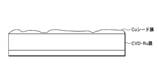
- the wettability of Cu to the sidewall of the trench or hole is actually deteriorated, and the trench or hole is filled with Cu plating. In some cases, voids may occur in the Cu plating.
- the present inventors first examined the cause of the deterioration of the wettability of Cu with respect to such a CVD-Ru film.
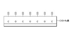
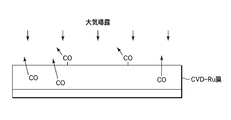
- a CVD-Ru film is formed using a film forming material containing an organometallic compound such as ruthenium carbonyl, since the film forming material contains a large amount of carbon, Then, carbon remains as an impurity in the film, and the film surface is terminated with CO.
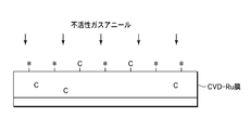
- annealing is performed in an inert gas atmosphere for Ru crystallization, the Ru film surface and the film It became clear that carbon was segregated inside, and the carbon remaining on the surface of the Ru film thus deteriorated the wettability of Cu.
- a step of forming a Ru film on a substrate by CVD using a film forming material containing an organometallic compound, and a substrate on which the Ru film is formed there is provided a method for forming a CVD-Ru film, which includes a step of performing annealing in a hydrogen-containing atmosphere.
- a process of forming a Ru film on a substrate by CVD using a film forming material containing an organometallic compound is inactive with respect to the substrate on which the Ru film is formed.
- a CVD-Ru film forming method including a step of annealing in a gas atmosphere, and a step of exposing the Ru film to the atmosphere after annealing in the inert gas atmosphere.
- a step of forming a metal barrier film on a substrate having trenches and / or holes, and a film forming material containing an organometallic compound on the metal barrier film are used.
- a method of manufacturing a semiconductor device including a step of forming a Cu seed film for embedding Cu plating in a hole.
- a metal barrier film is formed on a substrate having a trench and / or a hole, and a film forming material containing an organometallic compound is used on the metal barrier film.
- a step of forming a Ru film on the substrate by CVD, a step of annealing the substrate on which the Ru film is formed in an inert gas atmosphere, and after annealing in the inert gas atmosphere Provided is a method of manufacturing a semiconductor device, comprising: exposing the Ru film to the atmosphere; and forming a Cu seed film for embedding Cu plating in a trench and / or a hole on the annealed Ru film. Is done.
- a storage medium that operates on a computer and stores a program for controlling a processing apparatus, the program having a trench and / or a hole when executed.
- a step of forming a metal barrier film, a step of forming a Ru film on the substrate by CVD using a film forming material containing an organometallic compound on the metal barrier film, and the Ru film include: A step of annealing the formed substrate in a hydrogen-containing atmosphere, and a step of forming a Cu seed film for embedding Cu plating in trenches and / or holes on the annealed Ru film; A storage medium that causes a computer to control the processing apparatus is provided.
- a storage medium that operates on a computer and stores a program for controlling a processing apparatus, the program having a trench and / or a hole when executed.
- a step of forming a metal barrier film, a step of forming a Ru film on the substrate by CVD using a film forming material containing an organometallic compound on the metal barrier film, and the Ru film include: A step of annealing the formed substrate in an inert gas atmosphere, a step of exposing the Ru film to the atmosphere after annealing in the inert gas atmosphere, and an upper surface of the annealed Ru film
- the processing apparatus is controlled by a computer so that a method for manufacturing a semiconductor device including a step of forming a Cu seed film for embedding Cu plating in a trench and / or a hole is performed.
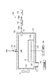
- FIG. 5 is a schematic diagram showing a state where annealing is performed in an inert gas atmosphere after the CVD-Ru film is formed.
- FIG. 6 is a schematic diagram showing a state in which a Cu seed film is formed on a CVD-Ru film after annealing in an inert gas atmosphere. It is a schematic diagram which shows a mode that Cu plating is embedded in the trench in which the Cu seed film
- FIG. 3 is a schematic diagram showing a state where annealing in a hydrogen atmosphere is performed after the CVD-Ru film is formed in the first embodiment of the present invention.
- FIG. 16 is a cross-sectional view showing a CVD-Ru film forming unit mounted on the processing apparatus of FIG.
- FIG. 16 is a cross-sectional view showing an annealing unit that is installed in the processing apparatus of FIG. 15 and performs annealing in the hydrogen-containing atmosphere of the first embodiment.
- FIG. 16 is a cross-sectional view illustrating an annealing unit that is installed in the processing apparatus of FIG. 15 and performs annealing according to the second embodiment.
- FIG. 1 is a flowchart showing a method according to the first embodiment of the present invention
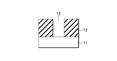
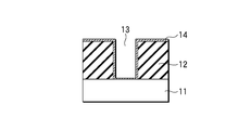
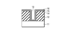
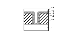
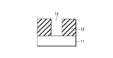
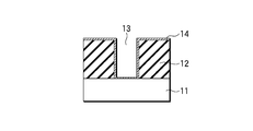
- FIGS. 2A to 2F are sectional views of the steps.
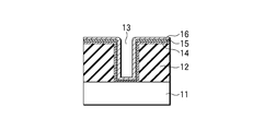
- a semiconductor wafer (hereinafter simply referred to as a wafer) having an interlayer insulating film 12 such as a SiO 2 film on a Si substrate 11 and having a trench 13 formed therein is prepared (step 1).
- a barrier film 14 of Ti or the like is formed on the entire surface including the trench 13 by PVD such as sputtering with a thickness of about 1 to 10 nm, for example, 4 nm (step 2, FIG. 2B).
- a CVD-Ru film 15 having a thickness of about 1 to 5 nm, for example, about 4 nm is formed on the barrier film 14 by using ruthenium carbonyl (Ru 3 (CO) 12 ), which is an organometallic compound, as a film forming material (step) 3, FIG. 2C).
- Ru 3 (CO) 12 ruthenium carbonyl
- the wafer on which the CVD-Ru film is formed is annealed in a hydrogen-containing atmosphere (step 4, FIG. 2D).
- a Cu seed film 16 is formed on the CVD-Ru film 15 with a thickness of about 5 to 50 nm, for example, about 20 nm by, for example, PVD (step 5, FIG. 2E).
- Cu plating 17 is applied on the Cu seed film 16 to fill the trench 13 (step 6, FIG. 2F).
- ruthenium carbonyl (Ru 3 (CO) 12 ) is supplied onto the barrier film 14 and thermally decomposed onto the barrier film 14.
- a CVD-Ru film 15 is formed.
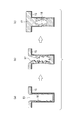
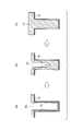
- FIG. 6A A state in which Cu plating is embedded in the trench 13 in which the Cu seed film 16 is formed in such a state will be described with reference to FIG.
- the discontinuity of the Cu seed film 16 on the CVD-Ru film 15 is conspicuous on the side wall of the trench 13, and the CVD-Ru film 15 is exposed to form RuO 2 . Since there is a portion which is formed, the resistance is large, and the current density in the trench 13 during Cu plating is lowered.
- FIG. 6B When Cu plating is started on the Cu seed film 16 in such a discontinuous state, as shown in FIG. 6B, the bottom-up during Cu plating is slow, the generation density of Cu nuclei is low, Voids are also generated.
- FIG. 6C the opening of the trench 13 is closed (pinch off) before the Cu plating is completely filled in the trench 13, and the center void 18 is generated. End up.
- Step 3 after the CVD-Ru film 15 is formed in Step 3, annealing is performed in a hydrogen-containing atmosphere in Step 4, so that C, O and Since CO on the surface is desorbed and Ru is crystallized, and C is released from the CVD-Ru film 15 by the action of hydrogen, segregation of the film surface and C in the film does not occur, and the surface of the CVD-Ru film 15 is It becomes a clean state.
- the Cu seed film 16 in step 5 is formed in this state, the surface of the CVD-Ru film 15 is clean, so that Cu is easily wetted. As shown in FIG. The whole is covered with an extremely thin Cu seed film 16.
- FIG. 9A the Cu seed film 16 on the CVD-Ru film 15 on the sidewall of the trench is continuous and relatively smooth, so the resistance is small and the Cu seed film 16 in the trench 13 during Cu plating is present.
- FIG. 9B the bottom-up and Cu nucleation of the Cu plating are smooth as shown in FIG. 9B, and the trench is formed without generating voids as shown in FIG. 9C. 13 can be filled.
- the annealing process in the hydrogen-containing atmosphere in Step 4 is preferably performed at 150 to 400 ° C. If it exceeds 400 ° C., the device may be adversely affected, and if it is less than 150 ° C., the effect of removing C may be insufficient.
- the gas forming the atmosphere may be only hydrogen gas, or other gas such as hydrogen gas and inert gas may be mixed.
- the hydrogen gas ratio at this time is preferably about 3 to 100%, and the hydrogen partial pressure is preferably about 4 to 1333 Pa.
- the annealing is performed in the hydrogen-containing atmosphere, so that the residual carbon on the Ru film surface is reduced, The wettability of the Cu seed film is improved. For this reason, bottom-up and nucleation during Cu plating proceed rapidly, and voids in Cu plating can be eliminated.
- FIG. 10 is a flowchart showing a method according to the second embodiment of the present invention
- FIGS. 11A to 11G are process sectional views thereof.
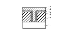
- a wafer similar to Step 1 of the first embodiment is prepared (Step 11, FIG. 11A), and a barrier film 14 is formed (Step 11) as in Step 2 of the first embodiment. 12, FIG. 11B), and then, a CVD-Ru film 15 is formed in the same manner as in Step 3 of the first embodiment (Step 13, FIG. 11C).
- annealing is performed in an inert gas, for example, an Ar gas atmosphere (step 14, FIG. 11D), and then the wafer is exposed to the atmosphere (step 15, FIG. 11E).
- a Cu seed film 16 is formed on the CVD-Ru film 15 (step 16, FIG. 11F), and then Cu plating 17 is applied on the Cu seed film 16.
- the trench 13 is filled (step 17, FIG. 11G).
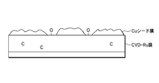
- step 14 annealing is performed in an inert gas atmosphere as in the prior art. Therefore, as shown in FIG. C segregates in the air, but as a result of exposure to the air in step 15 thereafter, the segregated C is desorbed as CO by oxygen in the air as shown in FIG. 12, and the surface of the CVD-Ru film 15 is clean. It becomes a state. Therefore, when the formation of the Cu seed film 16 in step 16 is performed, the entire surface of the CVD-Ru film 15 is covered with the ultrathin Cu seed film 16 as in the first embodiment. In the case of 17 Cu plating, bottom-up of Cu plating and Cu nucleation are smooth, and the trench 13 can be filled without generating voids.
- the annealing process in the inert gas atmosphere in step 14 is preferably performed at 150 to 400 ° C. If it exceeds 400 ° C., the device may be adversely affected, and if it is less than 150 ° C., the effect of removing C may be insufficient.
- the pressure in the chamber is preferably about 133 to 1333 Pa.
- the exposure to the atmosphere in step 15 may literally expose the silicon substrate to the atmosphere, or may introduce a slight amount of the atmosphere into the vacuum atmosphere chamber.
- a CVD-Ru film is formed using a film forming raw material containing an organometallic compound, and then annealed in an inert gas atmosphere, and then exposed to the atmosphere. Residual carbon on the film surface is reduced, and the wettability of the Cu seed film is improved. For this reason, bottom-up and nucleation during Cu plating proceed rapidly, and voids in Cu plating can be eliminated.
- a SiO 2 film which is an interlayer insulating film, is formed on a silicon substrate, a wafer having a trench is prepared, and a 4 nm-thick Ti film is formed by PVD as a barrier film, on which ruthenium carbonyl is formed.
- a CVD-Ru film having a thickness of 4 nm is formed using (Ru 3 (CO) 12 ) and then a Cu seed film having a thickness of 20 nm is formed, (1) a Cu seed film is formed without annealing.
- the C concentration in the film thickness direction was analyzed by a secondary ion mass spectrometer (SIMS).
- SIMS secondary ion mass spectrometer
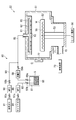
- FIG. 15 is a plan view showing such a multi-chamber processing apparatus.
- the processing apparatus 20 includes a PVD-Ti film forming unit 21, a CVD-Ru film forming unit 22, an annealing unit 23, and a Cu seed film forming unit 24, all of which are held in vacuum. These are connected to each side of the transfer chamber 25 having a hexagonal shape through a gate valve G. Two load lock chambers 26 and 27 are connected to the other side of the transfer chamber 25 via a gate valve G. The transfer chamber 25 is maintained in a vacuum. An air loading / unloading chamber 28 is provided on the opposite side of the load lock chambers 26, 27 from the transfer chamber 25, and a wafer is disposed on the opposite side of the loading / unloading chamber 28 from the connection portion of the load lock chambers 26, 27. Two carrier attachment ports 29 and 30 for attaching the carrier C capable of accommodating W are provided.
- the PVD-Ti film forming unit 21, the CVD-Ru film forming unit 22, the annealing unit 23, the Cu seed film forming unit 24, and the load lock chambers 26 and 27 are placed on the wafer W.
- a transfer device 32 for carrying in and out is provided.
- the transfer device 32 is provided in the approximate center of the transfer chamber 25, and has two support arms 34a and 34b that support the semiconductor wafer W at the tip of a rotatable / extensible / retractable portion 33 that can be rotated and extended. These two support arms 34a, 34b are attached to the rotation / extension / contraction section 33 so as to face in opposite directions.
- a transfer device 36 for loading / unloading the wafer W into / from the carrier C and loading / unloading the wafer W into / from the load lock chambers 26 and 27 is provided.
- the transfer device 36 has an articulated arm structure, and can run on the rail 38 along the arrangement direction of the carrier C.
- the wafer W is placed on the two support arms 37a and 37b at the tip thereof. Place and carry it.
- the processing apparatus 20 includes a control unit 40 that controls each component, and thereby, each component of the units 21 to 24, the transfer devices 32 and 36, an exhaust system (not shown) of the transfer chamber 25, Control such as opening and closing of the gate valve G is performed.
- the control unit 40 includes a process controller 41 including a microprocessor (computer), a user interface 42, and a storage unit 43. Each component of the processing device 20 is electrically connected to the process controller 41 and controlled.
- the user interface 42 is connected to the process controller 41, and visualizes the operation status of each component of the processing device 20 and a keyboard on which an operator inputs commands to manage each component of the processing device 20. It consists of a display that displays it.
- the storage unit 43 is also connected to the process controller 41, and in this storage unit 43, according to a control program and processing conditions for realizing various processes executed by the processing device 20 under the control of the process controller 41.
- a control program for causing each component of the processing device 20 to execute a predetermined process, that is, a processing recipe, various databases, and the like are stored.
- the processing recipe is stored in a storage medium (not shown) in the storage unit 43.
- the storage medium may be a fixed medium such as a hard disk or a portable medium such as a CDROM, DVD, or flash memory. Moreover, you may make it transmit a recipe suitably from another apparatus via a dedicated line, for example.
- a predetermined processing recipe is called from the storage unit 43 by an instruction from the user interface 42 and executed by the process controller 41, so that the desired processing in the processing device 20 is performed under the control of the process controller 41. Is performed.
- the wafer W taken out from the carrier C is transferred to one of the load lock chambers 26 and 27 by the transfer device 36 in the loading / unloading chamber 28, and the load lock chamber is evacuated. Then, the wafer is taken out by the transfer device 32 in the transfer chamber 25 and is first transferred to the PVD-Ti film forming unit 21 to form a Ti film as a barrier film on the interlayer insulating film of the wafer W, for example, the SiO 2 film. Film. Next, the wafer W after the Ti film is formed is transferred to the CVD-Ru film forming unit 22 to form a CVD-Ru film.
- the wafer W on which the Ru film is formed is transported to the annealing unit 23, and annealing treatment in a hydrogen-containing atmosphere or annealing in an inert gas atmosphere and exposure to the atmosphere are performed. Thereafter, the annealed wafer W is transferred to the Cu seed film forming unit 24, and a Cu seed film is formed on the CVD-Ru film by, for example, PVD.
- the wafer W thus formed up to the Cu seed film is transferred to one of the load lock chambers 26 and 27 by the transfer device 32, and the load lock chamber is brought to the atmosphere, and then the wafer is transferred by the transfer device 36. Return to Carrier C.
- the wafer thus formed up to the Cu seed film is transferred to the Cu plating facility while being accommodated in the carrier C, and is subjected to Cu plating.
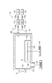
- FIG. 16 is a cross-sectional view showing a CVD-Ru film forming unit.
- the CVD-Ru film forming unit 22 has a substantially cylindrical chamber 51 which is airtightly configured.
- a susceptor 52 for horizontally supporting a wafer W which is a substrate to be processed is included therein. It arrange
- a heater 55 is embedded in the susceptor 52, and a heater power source 56 is connected to the heater 55.
- the heater power source 56 is controlled by a heater controller (not shown) based on a detection signal of a thermocouple (not shown) provided in the susceptor 52, so that the wafer W is controlled to a predetermined temperature. Yes.
- the susceptor 52 is provided with three wafer raising / lowering pins (not shown) for supporting the wafer W and raising / lowering it so as to protrude and retract with respect to the surface of the susceptor 52.
- a shower head 60 for introducing a processing gas for CVD film formation into the chamber 51 in a shower shape is provided on the top wall of the chamber 51 so as to face the susceptor 52.
- the shower head 60 is for discharging a film-forming gas supplied from a gas supply mechanism 80, which will be described later, into the chamber 51.
- a gas inlet 61 for introducing a film-forming gas is provided above the shower head 60.
- a gas diffusion space 62 is formed inside the shower head 60, and a number of gas discharge holes 63 are formed on the bottom surface thereof.
- An exhaust chamber 71 protruding downward is provided on the bottom wall of the chamber 51.
- An exhaust pipe 72 is connected to a side surface of the exhaust chamber 71, and an exhaust device 73 having a vacuum pump, a pressure control valve, and the like is connected to the exhaust pipe 72.
- an exhaust device 73 having a vacuum pump, a pressure control valve, and the like is connected to the exhaust pipe 72.
- the side wall of the chamber 51 is provided with a loading / unloading port 77 for loading / unloading the wafer W to / from the wafer transfer chamber 25 and a gate valve G for opening / closing the loading / unloading port 77.
- the gas supply mechanism 80 includes a film forming material container 81 that stores ruthenium carbonyl (Ru 3 (CO) 12 ) as a solid film forming material S.
- a heater 82 is provided around the film forming material container 81.
- a carrier gas pipe 83 is inserted into the film forming raw material container 81 from above, and for example, CO gas is blown into the film forming raw material container 81 as a carrier gas from the carrier gas source 84 through the carrier gas supply pipe 83. Yes.
- a gas supply pipe 85 is inserted into the film forming material container 81. The other end of the gas supply pipe 85 is connected to the gas inlet 61 of the shower head 60.
- the carrier gas by supplying the carrier gas into the film forming raw material container 81 via the carrier gas supply pipe 83, the ruthenium carbonyl (Ru 3 (CO) 12 ) gas sublimated in the film forming raw material container 81 is transferred to the carrier gas.
- the gas can be supplied into the chamber 51 through the gas supply pipe 85 and the shower head 60.
- the carrier gas supply pipe 83 is provided with a mass flow controller 86 for flow rate control and valves 87a and 87b before and after the mass flow controller 86. Further, the gas supply pipe 85 is provided with a flow meter 88 for grasping the amount of ruthenium carbonyl (Ru 3 (CO) 12 ) gas and valves 89 a and 89 b before and after the flow meter 88.
- ruthenium carbonyl Ru 3 (CO) 12
- a dilution gas supply pipe 90 for supplying a gas for appropriately diluting the film forming raw material gas is connected.
- a dilution gas source 91 for supplying a dilution gas composed of an inert gas such as Ar gas or N 2 gas is connected to the dilution gas supply pipe 90.
- the dilution gas source 91 is connected to the dilution gas supply pipe 90 via the dilution gas supply pipe 90.
- the source gas is diluted to an appropriate concentration.
- the dilution gas from the dilution gas source 91 also functions as a purge gas for purging the residual gas in the gas supply pipe 85 and the chamber 51.
- the dilution gas supply pipe 90 includes a mass flow controller 92 for flow rate control and valves 93a and 93b before and after the mass flow controller 92.
- another gas such as CO gas or H 2 gas, may be separately connected to the dilution gas supply pipe 90.
- the gate valve G is opened, and the wafer W after the barrier film deposition is loaded into the chamber 51 from the loading / unloading port 77, and on the susceptor 52. Place.
- the wafer W is heated to 150 to 250 ° C. via the susceptor 52 by the heater 55, the chamber 51 is evacuated by the vacuum pump of the evacuation device 73, and the pressure in the chamber 51 is evacuated to 2 to 67 Pa.
- valves 87 a and 87 b are opened, for example, CO gas is blown as a carrier gas into the film forming raw material container 81 through the carrier gas supply pipe 83, and sublimation is generated by heating the heater 82 in the film forming raw material container 81.
- the Ru 3 (CO) 12 gas is introduced into the chamber 51 through the gas supply pipe 85 and the shower head 60 in a state in which the gas is carried by the carrier gas.
- Ru generated by thermally decomposing Ru 3 (CO) 12 gas is deposited on the Ti film of the wafer W, and a CVD-Ru film having a predetermined film thickness is formed.
- the flow rate of the Ru 3 (CO) 12 gas at this time is preferably about 1 to 5 mL / min (sccm).
- a dilution gas may be introduced at a predetermined ratio.
- valves 87a and 87b are closed to stop the supply of Ru 3 (CO) 12 gas, and the dilution gas is supplied from the dilution gas supply source 91 as a purge gas in the chamber 52. And the Ru 3 (CO) 12 gas is purged, and then the gate valve G is opened and the wafer W is unloaded from the loading / unloading port 77.
- FIG. 17 is a cross-sectional view showing an annealing unit that is installed in the processing apparatus of FIG. 15 and performs annealing in the hydrogen-containing atmosphere of the first embodiment.
- This annealing unit has a substantially cylindrical chamber 101 which is hermetically configured, and a susceptor 102 for horizontally supporting a wafer W as a substrate to be processed is disposed at the bottom thereof.
- a heater 103 is embedded in the susceptor 102, and a heater power source 104 is connected to the heater 103.
- the heater power source 104 is controlled by a heater controller (not shown) based on a detection signal of a thermocouple (not shown) provided in the susceptor 102 to control the wafer W to a predetermined temperature.
- the susceptor 102 is provided with three wafer raising / lowering pins (not shown) for supporting the wafer W and raising / lowering it so as to protrude and retract with respect to the surface of the susceptor 102.
- a gas introduction member 105 is provided on the upper side wall of the chamber 101, and an atmosphere forming gas from the gas supply mechanism 110 is supplied into the chamber 101 through the gas introduction member 105.
- Gas supply mechanism 110 includes a H 2 gas supply source 112 has a H 2 gas supply pipe 111 extending from the H 2 supply source 112 to the gas introduction member 105, so as to introduce H 2 gas into the chamber 101 It has become.
- the H 2 gas supply pipe 111 is provided with a mass flow controller 113 for flow rate control and valves 114a and 114b before and after the mass flow controller 113.
- an Ar gas supply pipe 115 for supplying Ar gas as a dilution gas is connected to the H 2 gas supply pipe 111, and an Ar gas supply source 116 is connected to the Ar gas supply pipe 115. .
- the H 2 gas can be diluted with Ar gas and introduced into the chamber 101.
- the Ar gas supply pipe 115 is provided with a mass flow controller 117 for flow rate control and valves 118a and 118b before and after the mass flow controller 117.
- the diluent gas is not limited to Ar gas, and other rare gases or other inert gases such as N 2 gas can be used.
- An exhaust port 120 is provided on the bottom wall of the chamber 101, and an exhaust pipe 121 is connected to the exhaust port 120.
- An exhaust device 122 having a vacuum pump, a pressure control valve, and the like is connected to the exhaust pipe 121. By operating the exhaust device 122, the inside of the chamber 101 can be brought into a predetermined reduced pressure state.
- the side wall of the chamber 101 is provided with a loading / unloading port 123 for loading / unloading the wafer W to / from the wafer transfer chamber 25 and a gate valve G for opening / closing the loading / unloading port 123.
- the gate valve G is opened, and the wafer W after the CVD-Ru film formation is loaded into the chamber 101 from the loading / unloading port 123 and placed on the susceptor 102.
- the wafer W is heated to 150 to 400 ° C. through the susceptor 102 by the heater 103, the chamber 101 is evacuated by the vacuum pump of the exhaust device 122, and the pressure in the chamber 101 is evacuated to 133 to 1333 Pa, for example. To do.
- hydrogen gas is introduced into the chamber 101 at, for example, 10 to 1120 mL / min (sccm) and Ar gas as a dilution gas, for example, from 0 to 755 mL / min (sccm), and the hydrogen partial pressure is set to about 4 to 1333 Pa.
- Annealing is performed in a contained atmosphere.
- the supply of H 2 gas is stopped, the inside of the chamber 101 is purged with Ar gas, and then the gate valve G is opened and the wafer W is unloaded from the loading / unloading port 123.
- FIG. 18 is a cross-sectional view showing an annealing unit that is mounted on the processing apparatus of FIG. 15 and performs annealing according to the second embodiment.
- the basic structure of this annealing unit is the same as that of the annealing unit of FIG. 17, and the same components as those in FIG.
- This annealing unit has a gas supply mechanism 130 that supplies only Ar gas, which is an inert gas.
- the gas supply mechanism 130 has an Ar gas supply source 132 and an Ar gas supply pipe 131 extending from the Ar gas supply source 132 to the gas introduction unit 105, and introduces Ar gas into the chamber 101. Yes.
- the Ar gas pipe 131 is provided with a mass flow controller 133 for controlling the flow rate and valves 134a and 134b before and after the mass flow controller 133.
- the inert gas is not limited to Ar gas but may be other inert gas such as N 2 gas.
- An air introduction port 140 is provided on the top wall of the chamber 101, and an air introduction pipe 141 is connected to the air introduction port 140, and the atmosphere is introduced into the chamber 101 through the air introduction pipe 141. It is possible to introduce.
- the air introduction pipe 141 is provided with a valve 142.
- the gate valve G is opened, and the wafer W after the CVD-Ru film formation is loaded into the chamber 101 from the loading / unloading port 123 and placed on the susceptor 102.
- the wafer W is heated to 150 to 400 ° C. through the susceptor 102 by the heater 103, the chamber 101 is evacuated by the vacuum pump of the exhaust device 122, and the pressure in the chamber 101 is evacuated to 133 to 1333 Pa, for example. To do.
- Ar gas is introduced into the chamber 101 at a flow rate of 7 to 755 mL / min (sccm), for example, and the pressure in the chamber 101 is set to about 133 to 1333 Pa, and annealing is performed in an inert gas atmosphere.
- sccm mL / min
- annealing is performed in an inert gas atmosphere.
- the valve 142 is opened, the atmosphere is introduced into the chamber 101 through the atmosphere introduction pipe 141, and the wafer W is exposed to the atmosphere.
- segregated C is desorbed as CO by oxygen in the atmosphere, and the surface of the CVD-Ru film becomes clean. Therefore, when the Cu seed film is subsequently formed, Cu is easily wetted, and the entire surface of the CVD-Ru film can be covered with an extremely thin Cu seed film.
- the gate valve G is opened and the wafer W is unloaded from the loading / unloading port 123.
- this invention can be variously deformed, without being limited to the said embodiment.
- ruthenium carbonyl Ru 3 (CO) 12
- the present invention is not limited thereto, and a ruthenium pentadienyl compound is used.
- Other organic metal compounds may be used as film forming raw materials.
- the CVD-Ru film and the Cu seed film are formed on the wafer in which the trench is formed.
- the wafer may be a wafer having holes or a wafer having trenches and holes.
Landscapes
- Engineering & Computer Science (AREA)
- Chemical & Material Sciences (AREA)
- Condensed Matter Physics & Semiconductors (AREA)
- General Physics & Mathematics (AREA)
- Physics & Mathematics (AREA)
- Computer Hardware Design (AREA)
- Microelectronics & Electronic Packaging (AREA)
- Power Engineering (AREA)
- Manufacturing & Machinery (AREA)
- Chemical Kinetics & Catalysis (AREA)
- General Chemical & Material Sciences (AREA)
- Materials Engineering (AREA)
- Mechanical Engineering (AREA)
- Metallurgy (AREA)
- Organic Chemistry (AREA)
- Electrodes Of Semiconductors (AREA)
- Internal Circuitry In Semiconductor Integrated Circuit Devices (AREA)
- Chemical Vapour Deposition (AREA)
Priority Applications (3)
| Application Number | Priority Date | Filing Date | Title |
|---|---|---|---|
| CN2010800112191A CN102349138A (zh) | 2009-03-12 | 2010-02-25 | CVD-Ru膜的形成方法和半导体装置的制造方法 |
| KR1020117021177A KR101291821B1 (ko) | 2009-03-12 | 2010-02-25 | CVD-Ru막의 형성 방법 및 반도체 장치의 제조 방법 |
| US13/230,351 US20120064717A1 (en) | 2009-03-12 | 2011-09-12 | Method for forming cvd-ru film and method for manufacturing semiconductor devices |
Applications Claiming Priority (2)
| Application Number | Priority Date | Filing Date | Title |
|---|---|---|---|
| JP2009-059605 | 2009-03-12 | ||
| JP2009059605A JP5193913B2 (ja) | 2009-03-12 | 2009-03-12 | CVD−Ru膜の形成方法および半導体装置の製造方法 |
Related Child Applications (1)
| Application Number | Title | Priority Date | Filing Date |
|---|---|---|---|
| US13/230,351 Continuation US20120064717A1 (en) | 2009-03-12 | 2011-09-12 | Method for forming cvd-ru film and method for manufacturing semiconductor devices |
Publications (1)
| Publication Number | Publication Date |
|---|---|
| WO2010103930A1 true WO2010103930A1 (ja) | 2010-09-16 |
Family
ID=42728220
Family Applications (1)
| Application Number | Title | Priority Date | Filing Date |
|---|---|---|---|
| PCT/JP2010/052938 Ceased WO2010103930A1 (ja) | 2009-03-12 | 2010-02-25 | CVD-Ru膜の形成方法および半導体装置の製造方法 |
Country Status (6)
| Country | Link |
|---|---|
| US (1) | US20120064717A1 (enExample) |
| JP (1) | JP5193913B2 (enExample) |
| KR (1) | KR101291821B1 (enExample) |
| CN (1) | CN102349138A (enExample) |
| TW (1) | TWI467044B (enExample) |
| WO (1) | WO2010103930A1 (enExample) |
Families Citing this family (21)
| Publication number | Priority date | Publication date | Assignee | Title |
|---|---|---|---|---|
| WO2012133400A1 (ja) * | 2011-03-30 | 2012-10-04 | 東京エレクトロン株式会社 | Cu配線の形成方法 |
| US20130146468A1 (en) * | 2011-12-08 | 2013-06-13 | Applied Materials, Inc. | Chemical vapor deposition (cvd) of ruthenium films and applications for same |
| US8517769B1 (en) | 2012-03-16 | 2013-08-27 | Globalfoundries Inc. | Methods of forming copper-based conductive structures on an integrated circuit device |
| US8673766B2 (en) * | 2012-05-21 | 2014-03-18 | Globalfoundries Inc. | Methods of forming copper-based conductive structures by forming a copper-based seed layer having an as-deposited thickness profile and thereafter performing an etching process and electroless copper deposition |
| JP2014017345A (ja) * | 2012-07-09 | 2014-01-30 | Tokyo Electron Ltd | Cu配線の形成方法 |
| JP2015160963A (ja) * | 2014-02-26 | 2015-09-07 | 東京エレクトロン株式会社 | ルテニウム膜の成膜方法および成膜装置、ならびに半導体装置の製造方法 |
| EP3216050B1 (en) | 2014-11-05 | 2021-09-08 | Corning Incorporated | Bottom-up electrolytic via plating method |
| JP6467239B2 (ja) | 2015-02-16 | 2019-02-06 | 東京エレクトロン株式会社 | ルテニウム膜の成膜方法、成膜装置及び半導体装置の製造方法 |
| KR102324826B1 (ko) | 2015-04-02 | 2021-11-11 | 삼성전자주식회사 | 배선 구조물, 배선 구조물 형성 방법 및 반도체 장치의 제조 방법 |
| JP6419644B2 (ja) | 2015-05-21 | 2018-11-07 | 東京エレクトロン株式会社 | 金属ナノドットの形成方法、金属ナノドット形成装置及び半導体装置の製造方法 |
| US9805976B2 (en) | 2016-01-08 | 2017-10-31 | Applied Materials, Inc. | Co or Ni and Cu integration for small and large features in integrated circuits |
| WO2017143180A1 (en) * | 2016-02-19 | 2017-08-24 | Tokyo Electron Limited | Ruthenium metal deposition method for electrical connections |
| US20170241019A1 (en) * | 2016-02-22 | 2017-08-24 | Ultratech, Inc. | Pe-ald methods with reduced quartz-based contamination |
| JP6470876B2 (ja) * | 2016-05-16 | 2019-02-13 | 株式会社アルバック | Cu膜の形成方法 |
| JP6785130B2 (ja) * | 2016-07-06 | 2020-11-18 | 東京エレクトロン株式会社 | ルテニウム配線およびその製造方法 |
| JP6807251B2 (ja) | 2017-03-02 | 2021-01-06 | 東京エレクトロン株式会社 | ルテニウム配線の製造方法 |
| JP7277871B2 (ja) | 2017-10-04 | 2023-05-19 | 東京エレクトロン株式会社 | 相互接続のためのルテニウム金属機能フィリング |
| US10917966B2 (en) | 2018-01-29 | 2021-02-09 | Corning Incorporated | Articles including metallized vias |
| JP2020147772A (ja) * | 2019-03-11 | 2020-09-17 | 東京エレクトロン株式会社 | 成膜装置及び成膜方法 |
| US20220139776A1 (en) * | 2020-11-03 | 2022-05-05 | Tokyo Electron Limited | Method for filling recessed features in semiconductor devices with a low-resistivity metal |
| JP2022152438A (ja) * | 2021-03-29 | 2022-10-12 | 東京エレクトロン株式会社 | ルテニウム膜の成膜方法及び処理装置 |
Citations (7)
| Publication number | Priority date | Publication date | Assignee | Title |
|---|---|---|---|---|
| JP2001234347A (ja) * | 1999-12-23 | 2001-08-31 | Samsung Electronics Co Ltd | 工程条件を変化させつつ化学気相蒸着法でルテニウム膜を形成する方法及びそれにより形成されたルテニウム膜 |
| JP2003133438A (ja) * | 2001-10-30 | 2003-05-09 | Fujitsu Ltd | 容量素子及びその製造方法並びに半導体装置の製造方法 |
| JP2005029821A (ja) * | 2003-07-09 | 2005-02-03 | Tokyo Electron Ltd | 成膜方法 |
| WO2006101129A1 (ja) * | 2005-03-23 | 2006-09-28 | Tokyo Electron Limited | 基板処理方法、成膜方法、成膜装置及びコンピュータプログラム |
| JP2007507613A (ja) * | 2003-09-30 | 2007-03-29 | 東京エレクトロン株式会社 | シーケンシャル流量堆積を使用して金属層を堆積させる方法。 |
| JP2008041700A (ja) * | 2006-08-01 | 2008-02-21 | Tokyo Electron Ltd | 成膜方法、成膜装置及び記憶媒体 |
| JP2008244017A (ja) * | 2007-03-26 | 2008-10-09 | Ulvac Japan Ltd | 半導体装置の製造方法 |
Family Cites Families (2)
| Publication number | Priority date | Publication date | Assignee | Title |
|---|---|---|---|---|
| US20070069383A1 (en) * | 2005-09-28 | 2007-03-29 | Tokyo Electron Limited | Semiconductor device containing a ruthenium diffusion barrier and method of forming |
| US7476615B2 (en) * | 2006-11-01 | 2009-01-13 | Intel Corporation | Deposition process for iodine-doped ruthenium barrier layers |
-
2009
- 2009-03-12 JP JP2009059605A patent/JP5193913B2/ja not_active Expired - Fee Related
-
2010
- 2010-02-25 CN CN2010800112191A patent/CN102349138A/zh active Pending
- 2010-02-25 WO PCT/JP2010/052938 patent/WO2010103930A1/ja not_active Ceased
- 2010-02-25 KR KR1020117021177A patent/KR101291821B1/ko active Active
- 2010-03-11 TW TW99107153A patent/TWI467044B/zh active
-
2011
- 2011-09-12 US US13/230,351 patent/US20120064717A1/en not_active Abandoned
Patent Citations (7)
| Publication number | Priority date | Publication date | Assignee | Title |
|---|---|---|---|---|
| JP2001234347A (ja) * | 1999-12-23 | 2001-08-31 | Samsung Electronics Co Ltd | 工程条件を変化させつつ化学気相蒸着法でルテニウム膜を形成する方法及びそれにより形成されたルテニウム膜 |
| JP2003133438A (ja) * | 2001-10-30 | 2003-05-09 | Fujitsu Ltd | 容量素子及びその製造方法並びに半導体装置の製造方法 |
| JP2005029821A (ja) * | 2003-07-09 | 2005-02-03 | Tokyo Electron Ltd | 成膜方法 |
| JP2007507613A (ja) * | 2003-09-30 | 2007-03-29 | 東京エレクトロン株式会社 | シーケンシャル流量堆積を使用して金属層を堆積させる方法。 |
| WO2006101129A1 (ja) * | 2005-03-23 | 2006-09-28 | Tokyo Electron Limited | 基板処理方法、成膜方法、成膜装置及びコンピュータプログラム |
| JP2008041700A (ja) * | 2006-08-01 | 2008-02-21 | Tokyo Electron Ltd | 成膜方法、成膜装置及び記憶媒体 |
| JP2008244017A (ja) * | 2007-03-26 | 2008-10-09 | Ulvac Japan Ltd | 半導体装置の製造方法 |
Also Published As
| Publication number | Publication date |
|---|---|
| TW201043721A (en) | 2010-12-16 |
| TWI467044B (zh) | 2015-01-01 |
| US20120064717A1 (en) | 2012-03-15 |
| JP5193913B2 (ja) | 2013-05-08 |
| JP2010212601A (ja) | 2010-09-24 |
| KR20110124304A (ko) | 2011-11-16 |
| CN102349138A (zh) | 2012-02-08 |
| KR101291821B1 (ko) | 2013-07-31 |
Similar Documents
| Publication | Publication Date | Title |
|---|---|---|
| JP5193913B2 (ja) | CVD−Ru膜の形成方法および半導体装置の製造方法 | |
| US7791202B2 (en) | Semiconductor device having oxidized metal film and manufacture method of the same | |
| TWI469218B (zh) | Semiconductor device manufacturing method, semiconductor device, electronic device, semiconductor manufacturing device and memory medium | |
| JP6467239B2 (ja) | ルテニウム膜の成膜方法、成膜装置及び半導体装置の製造方法 | |
| JP4294696B2 (ja) | 半導体装置の製造方法および製造装置、ならびに記憶媒体 | |
| KR20140143095A (ko) | 산화 망간막의 형성 방법 | |
| US20250034715A1 (en) | Film forming method | |
| JP2016037656A (ja) | タングステン膜の成膜方法 | |
| KR101730229B1 (ko) | 루테늄막의 성막 방법 및 성막 장치와 반도체 장치의 제조 방법 | |
| US10096548B2 (en) | Method of manufacturing Cu wiring | |
| JP6013901B2 (ja) | Cu配線の形成方法 | |
| CN101689490B (zh) | 成膜方法和处理系统 | |
| JP6584326B2 (ja) | Cu配線の製造方法 | |
| JP2017050304A (ja) | 半導体装置の製造方法 | |
| JP6253214B2 (ja) | 半導体装置の製造方法、基板処理装置および記録媒体 | |
| US7846839B2 (en) | Film forming method, semiconductor device manufacturing method, semiconductor device, program and recording medium | |
| US20250197990A1 (en) | Film formation method and film formation device |
Legal Events
| Date | Code | Title | Description |
|---|---|---|---|
| WWE | Wipo information: entry into national phase |
Ref document number: 201080011219.1 Country of ref document: CN |
|
| 121 | Ep: the epo has been informed by wipo that ep was designated in this application |
Ref document number: 10750684 Country of ref document: EP Kind code of ref document: A1 |
|
| ENP | Entry into the national phase |
Ref document number: 20117021177 Country of ref document: KR Kind code of ref document: A |
|
| NENP | Non-entry into the national phase |
Ref country code: DE |
|
| 122 | Ep: pct application non-entry in european phase |
Ref document number: 10750684 Country of ref document: EP Kind code of ref document: A1 |