WO2010050130A1 - 半導体装置及びその製造方法 - Google Patents
半導体装置及びその製造方法 Download PDFInfo
- Publication number
- WO2010050130A1 WO2010050130A1 PCT/JP2009/005316 JP2009005316W WO2010050130A1 WO 2010050130 A1 WO2010050130 A1 WO 2010050130A1 JP 2009005316 W JP2009005316 W JP 2009005316W WO 2010050130 A1 WO2010050130 A1 WO 2010050130A1
- Authority
- WO
- WIPO (PCT)
- Prior art keywords
- layer
- active region
- crystal defect
- defect layer
- igbt
- Prior art date
- Legal status (The legal status is an assumption and is not a legal conclusion. Google has not performed a legal analysis and makes no representation as to the accuracy of the status listed.)
- Ceased
Links
Images

Classifications
-
- H—ELECTRICITY
- H10—SEMICONDUCTOR DEVICES; ELECTRIC SOLID-STATE DEVICES NOT OTHERWISE PROVIDED FOR
- H10D—INORGANIC ELECTRIC SEMICONDUCTOR DEVICES
- H10D48/00—Individual devices not covered by groups H10D1/00 - H10D44/00
- H10D48/30—Devices controlled by electric currents or voltages
- H10D48/32—Devices controlled by only the electric current supplied, or only the electric potential applied, to an electrode which does not carry the current to be rectified, amplified or switched
- H10D48/34—Bipolar devices
- H10D48/345—Bipolar transistors having ohmic electrodes on emitter-like, base-like, and collector-like regions
-
- H—ELECTRICITY
- H10—SEMICONDUCTOR DEVICES; ELECTRIC SOLID-STATE DEVICES NOT OTHERWISE PROVIDED FOR
- H10D—INORGANIC ELECTRIC SEMICONDUCTOR DEVICES
- H10D12/00—Bipolar devices controlled by the field effect, e.g. insulated-gate bipolar transistors [IGBT]
- H10D12/411—Insulated-gate bipolar transistors [IGBT]
- H10D12/441—Vertical IGBTs
-
- H—ELECTRICITY
- H10—SEMICONDUCTOR DEVICES; ELECTRIC SOLID-STATE DEVICES NOT OTHERWISE PROVIDED FOR
- H10D—INORGANIC ELECTRIC SEMICONDUCTOR DEVICES
- H10D12/00—Bipolar devices controlled by the field effect, e.g. insulated-gate bipolar transistors [IGBT]
- H10D12/01—Manufacture or treatment
- H10D12/031—Manufacture or treatment of IGBTs
- H10D12/032—Manufacture or treatment of IGBTs of vertical IGBTs
-
- H—ELECTRICITY
- H10—SEMICONDUCTOR DEVICES; ELECTRIC SOLID-STATE DEVICES NOT OTHERWISE PROVIDED FOR
- H10D—INORGANIC ELECTRIC SEMICONDUCTOR DEVICES
- H10D62/00—Semiconductor bodies, or regions thereof, of devices having potential barriers
- H10D62/10—Shapes, relative sizes or dispositions of the regions of the semiconductor bodies; Shapes of the semiconductor bodies
- H10D62/102—Constructional design considerations for preventing surface leakage or controlling electric field concentration
- H10D62/103—Constructional design considerations for preventing surface leakage or controlling electric field concentration for increasing or controlling the breakdown voltage of reverse-biased devices
- H10D62/105—Constructional design considerations for preventing surface leakage or controlling electric field concentration for increasing or controlling the breakdown voltage of reverse-biased devices by having particular doping profiles, shapes or arrangements of PN junctions; by having supplementary regions, e.g. junction termination extension [JTE]
- H10D62/106—Constructional design considerations for preventing surface leakage or controlling electric field concentration for increasing or controlling the breakdown voltage of reverse-biased devices by having particular doping profiles, shapes or arrangements of PN junctions; by having supplementary regions, e.g. junction termination extension [JTE] having supplementary regions doped oppositely to or in rectifying contact with regions of the semiconductor bodies, e.g. guard rings with PN or Schottky junctions
-
- H—ELECTRICITY
- H10—SEMICONDUCTOR DEVICES; ELECTRIC SOLID-STATE DEVICES NOT OTHERWISE PROVIDED FOR
- H10D—INORGANIC ELECTRIC SEMICONDUCTOR DEVICES
- H10D62/00—Semiconductor bodies, or regions thereof, of devices having potential barriers
- H10D62/10—Shapes, relative sizes or dispositions of the regions of the semiconductor bodies; Shapes of the semiconductor bodies
- H10D62/13—Semiconductor regions connected to electrodes carrying current to be rectified, amplified or switched, e.g. source or drain regions
- H10D62/141—Anode or cathode regions of thyristors; Collector or emitter regions of gated bipolar-mode devices, e.g. of IGBTs
- H10D62/142—Anode regions of thyristors or collector regions of gated bipolar-mode devices
-
- H—ELECTRICITY
- H10—SEMICONDUCTOR DEVICES; ELECTRIC SOLID-STATE DEVICES NOT OTHERWISE PROVIDED FOR
- H10D—INORGANIC ELECTRIC SEMICONDUCTOR DEVICES
- H10D62/00—Semiconductor bodies, or regions thereof, of devices having potential barriers
- H10D62/50—Physical imperfections
- H10D62/53—Physical imperfections the imperfections being within the semiconductor body
-
- H—ELECTRICITY
- H10—SEMICONDUCTOR DEVICES; ELECTRIC SOLID-STATE DEVICES NOT OTHERWISE PROVIDED FOR
- H10P—GENERIC PROCESSES OR APPARATUS FOR THE MANUFACTURE OR TREATMENT OF DEVICES COVERED BY CLASS H10
- H10P10/00—Bonding of wafers, substrates or parts of devices
Definitions
- the present invention relates to a structure of a semiconductor device, in particular, an insulated gate bipolar transistor that can be operated with a large current, and a manufacturing method thereof.
- IGBT insulated gate bipolar transistor
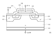
- FIG. 4 is an example of a cross-sectional structure of a typical IGBT element.
- the function of a bipolar transistor is combined with the function of an insulated gate transistor (Metal Oxide Field Effect Transistor: MOSFET).
- MOSFET Metal Oxide Field Effect Transistor
- an n layer 102 serving as a base is formed on a p-type substrate 101 serving as a collector of a bipolar transistor, a p + layer 103 serving as an emitter, an n + layer 104, a gate oxide film 105 serving as a part of a MOSFET, 106 is formed on the surface side (upper side in FIG. 4).
- An emitter electrode 107 is connected to the p + layer 103 and the n + layer 104, and an insulating layer 108 for preventing a short circuit between the emitter electrode 107 and the gate electrode 106 is formed.
- the IGBT 100 is turned on when its gate voltage is equal to or higher than a threshold value. At this time, conductivity is modulated by injecting holes from the p-type substrate 101 into the n layer 102, and a large current flows, that is, the on-resistance can be lowered. Therefore, the ON resistance (ON voltage) can be lowered by increasing the amount of injected holes. Actually, in many cases, the on-resistance is particularly lowered by forming a plurality of IGBT elements 100 having the above-described configuration on the same substrate and connecting them in parallel.
- the gate voltage is turned off by making it smaller than the threshold value.
- the holes existing at the time of turning on the n layer 102 disappear, Current flows. That is, the holes recombine with electrons and disappear, but the IGBT 100 is not completely turned off until the holes disappear. Therefore, in order to improve the switching speed of the IGBT, it is necessary to shorten the time until the holes disappear (the lifetime of the holes).
- Patent Document 1 describes a technique for forming a crystal defect layer having a short hole lifetime in an n layer by ion implantation.
- Patent Document 2 describes a technique for forming a similar crystal defect layer on the p-type substrate side. By using such a technique, the switching performance of the IGBT element 100 could be improved.
- holes in the base n layer 102 contribute to lowering the switching speed, they also directly contribute to lowering the on-resistance due to the operation principle of the IGBT. Therefore, by shortening the lifetime of holes in the n layer 102 or limiting the injection amount, the switching speed is improved, but the on-resistance is increased. That is, in the above technique, the switching speed and the on-resistance are in a trade-off relationship.
- the present invention has been made in view of such problems, and an object thereof is to provide an invention that solves the above problems.
- a semiconductor device has a configuration in which an n-layer is formed on a p-type substrate, an emitter and a gate are formed on the surface side using the p-type substrate as a collector and the n-layer as a base.
- the crystal defect layer in the active region is formed at a position shallower than the crystal defect layer in the non-active region, which is a region where the insulated gate bipolar transistor element is not formed, in the semiconductor substrate. It is characterized by that.
- the crystal defect layer is formed in the active region and the inactive region so that a hole injection amount in the inactive region is smaller than a hole injection amount in the active region. It is characterized by that.
- the emitter common electrode connected to the emitter of the insulated gate bipolar transistor element formed in the active region is formed of a material having higher ion blocking ability than the semiconductor substrate. .
- the semiconductor device of the present invention is characterized in that the emitter common electrode includes nickel or an alloy containing nickel.
- an emitter and a gate are formed on a surface side of a semiconductor substrate having a configuration in which an n layer is formed on a p type substrate, the p type substrate as a collector, and the n layer as a base.
- a method of manufacturing a semiconductor device comprising an insulated gate bipolar transistor element having a structure as described above, wherein a crystal defect layer in which many crystal defects are introduced is formed in the semiconductor substrate, wherein the insulated gate bipolar transistor is formed on the semiconductor substrate.
- a transistor forming step for forming a transistor element an electrode forming step for forming an emitter common electrode connected to an emitter of the insulated gate bipolar transistor element on the insulated gate bipolar transistor element, and ion implantation from the surface side
- An ion implantation step of forming the crystal defect layer in the semiconductor substrate Characterized in that it Bei.
- the present invention is configured as described above, an IGBT having both high switching speed and low on-resistance (on voltage) can be obtained.
- IGBT Insulated Gate Bipolar Transistor
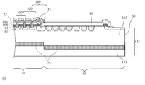
- a plurality of IGBT elements 100 having the same structure as in FIG. 4 are arranged on the left side in FIG. 1 in the semiconductor (silicon) substrate 11, and there is a region (active region 20) connected in parallel. .
- one emitter region in FIG. 4 is shared by adjacent IGBT elements, and the emitter electrode is shared by all IGBT elements 100.
- the right side in FIG. 1 is a chip outer peripheral portion (end portion) 30, and no IGBT element is formed in a region (inactive region 40) between the active region 20 and the chip outer peripheral portion 30.
- guard ring p layers 41 formed as guard rings for maintaining a withstand voltage are formed between the chip outer peripheral portion 30 and the active region 20 so as to surround the active region 20.
- the guard ring p layer 41 does not affect individual operations of the IGBT element 100.
- the semiconductor substrate 11 used in the above structure is composed of two layers, a p-type substrate 101 serving as a collector and an n layer 102 serving as a base. That is, they exist uniformly in the active region 20 and the non-active region 40.
- each p + layer 103, the n + layer 104, the gate oxide film 105, and the gate 106 shown in FIG. 4 are formed for each individual IGBT element.
- each p + layer 103 and each n + layer 104 serving as an emitter are connected by the emitter common electrode 21.
- each gate 106 is also connected by a gate electrode (not shown).
- an insulating layer 22 in which the insulating layers in FIG. 4 are integrated is formed on the entire surface so that the emitter common electrode 21 and the gate electrode do not short-circuit.
- the crystal defect layer 25 is formed in the n layer 102 in the active region 20 and in the p-type substrate 101 in the inactive region 40. That is, the crystal defect layer 25 in the active region 20 is formed at a position shallower than the crystal defect layer 25 in the non-active region 40 when viewed from the surface of the IGBT 10.
- the crystal defect layer 25 is a layer into which many crystal defects introduced into the n layer 102 or the p-type substrate 101 by ion implantation of light elements such as hydrogen and helium, for example. The depth at which this layer is formed is determined by the range of light elements implanted with ions. Further, the crystal defect layer 25 has a spread according to the distribution of implanted ions in the vertical direction in FIG.
- the crystal defect layer 25 is also introduced into the IGBT 10, unlike the structure described in Patent Document 1, a location where the crystal defect layer 25 is formed in the active region 20 and the inactive region 40 (FIG. 1). The depth inside is different. This operation will be described below.
- the amount of holes injected into the n layer 102 is affected by the presence thereof. At this time, the effect varies depending on the depth at which the crystal defect layer 25 exists. For example, when the crystal defect layer 25 is in the n layer 102, holes injected from the interface (pn junction) between the p-type substrate 101 and the n layer 102 are trapped in the crystal defect in the crystal defect layer 25. Is done. However, since the holes are injected from the p-type substrate 101 into the n layer 102 by diffusion from the lower side to the upper side in FIG. 1, the concentration thereof is higher as it is closer to the pn junction.
- the effect of reducing the amount of hole injection is greater when the crystal defect layer 25 is located near the pn junction. Therefore, when the crystal defect layer 25 is formed in the n layer 102, the amount of hole injection becomes smaller as the crystal defect layer 25 is closer to the pn junction.
- the crystal defect layer 25 when the crystal defect layer 25 is formed in the p-type substrate 101, the number of holes to be injected in the crystal defect layer 25 is small. Accordingly, even when the crystal defect layer 25 is in the p-type substrate 101, the amount of hole injection is affected. For example, when the crystal defect layer 25 is located at a position away from the pn junction in the p-type substrate 101 (when the crystal defect layer 25 is on the lower side in FIG. 1), the crystal closer to the pn junction than the crystal defect layer 25 Since the influence of the defect-free p-layer increases, the amount of hole injection increases as the crystal defect layer 25 moves away from the pn junction.
- the change in the amount of hole injection according to the distance from the pn junction of the crystal defect layer 25 indicates that the crystal defect layer 25 is p-type. The same applies to the case in the substrate 101.
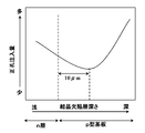
- the crystal defect layer 25 when the crystal defect layer 25 is located near the pn junction, the amount of hole injection is reduced, and the crystal defect layer 25 is located on the upper side or lower side in FIG. 1 from the interface between the p-type substrate 101 and the n layer 102. In the case where the distance between them is far away, the amount of hole injection increases. Therefore, the relationship between the depth of the crystal defect layer 25 and the amount of hole injection is conceptually as shown in FIG. However, as described above, the mechanism in which the crystal defect layer 25 affects the amount of hole injection differs between the case where the crystal defect layer 25 is in the n layer 102 and the case where it is in the p-type substrate 101, so that the pn junction is the center. It is not a symmetrical property.
- the depth at which the amount of hole injection is minimized does not coincide with the pn junction, and the depth is affected by the element structure.
- it is the impurity concentration of the p-type substrate 101 that has the greatest influence on this depth, and when this is high, it tends to be shallow.
- this is 1 ⁇ 10 18 to 10 19 cm ⁇ 3
- the depth is about 10 ⁇ m from the pn junction to the p-type substrate 101 side as shown in FIG.
- the hole injection amount contributes to reducing the on-resistance of the IGBT 10, but also causes a decrease in switching speed.
- it is the holes injected mainly at the location (active region 20) where the IGBT element 100 is formed that contributes to the reduction of the on-resistance, that is, the increase of the operating current, and is inactive.
- the rate at which holes injected in region 40 contribute to this is small.
- the holes injected in the inactive region 40 remain at the time of OFF, the current flowing through the IGBT element 100 is difficult to attenuate and has a skirted state, that is, the switching time becomes long.
- the influence of holes injected in the inactive region 40 on the on-resistance is small, but the influence of the holes on the switching time is large. Therefore, if the hole injection amount in the non-active region 40 is smaller than that in the active region 20, the switching speed can be increased while keeping the on-resistance low.
- the hole injection amount is reduced in the inactive region 40, so that the switching speed is increased.
- the decrease in the amount of hole injection in the active region 20 is smaller than that in the non-active region 40. Therefore, an increase in on-resistance at this time is suppressed.
- the crystal defect layer 25 in the active region 20 is formed near the pn junction in the n layer 102 and is formed near the pn junction in the non-active region 40.
- the present invention is not limited to this. Absent.
- the hole injection amount at the position of the crystal defect layer 25 in the inactive region 40 is smaller than the hole injection amount at the position of the crystal defect layer 25 in the active region 20 in the characteristics of FIG. Similar effects can be obtained.
- the crystal defect layer 25 is formed in the n layer 102 in both the active region 20 and the non-active region 40, and the crystal defect layer 25 in the active region 20 is located at a shallower position (upper side in FIG. 1). A similar effect can be obtained.
- the crystal defect layer 25 in the non-active region 40 is formed about 10 ⁇ m below the pn junction and the crystal defect layer 25 in the active region 20 is formed at a shallower position. Therefore, when the crystal defect layer 25 in the non-active region 40 is formed at a depth within 10 ⁇ m from the pn junction and the crystal defect layer 25 in the active region 20 is formed at a shallower portion, the same applies. The effect of.
- the parasitic transistor effect and latch-up are also suppressed by reducing the amount of hole injection in the active region 20. Accordingly, the breakdown resistance of the IGBT can be improved.
- an IGBT that operates in a non-punch through type, whose operation is mainly determined by the amount of hole injection from the p-type substrate 101 (emitter) side.
- the structure of the present embodiment is similarly applied to an IGBT that performs a punch-through type operation or a light punch-through type IGBT whose operation is mainly determined by the lifetime of holes in the n layer 102. It is clear that is effective. It is also clear that the present invention is similarly effective for a trench IGBT in which a MOS part is highly integrated using a trench structure.
- the example in which the above structure is formed on a p-type substrate has been described.
- an intrinsic substrate is used instead of the p-type substrate, and impurity diffusion or the like is performed thereon to form a p-layer. It is clear that the same effect can be obtained even when the above structure is formed after the formation. That is, the configuration of the semiconductor substrate is arbitrary as long as the above operation can be performed.
- FIG. 3 is a process cross-sectional view schematically showing this manufacturing method.
- a gate, an emitter region, and the like in the IGBT are formed on the semiconductor substrate 11 (transistor forming step).
- This manufacturing process is the same as that described in Patent Document 1, for example. That is, an n layer 102 is formed by epitaxial growth on a silicon p-type substrate 101, which becomes a semiconductor substrate 11.
- boron and the like are selectively ion-implanted to form the p + layer 103, and phosphorus and arsenic are similarly ion-implanted to form the n + layer 104.
- the gate 106 is formed by forming polysilicon on the gate oxide film 105 by a CVD (Chemical Vapor Deposition) method or the like and then selectively etching it.
- CVD Chemical Vapor Deposition
- a step of electrically connecting the IGBT elements 100 is performed.
- the insulating layer 22 is formed on the entire surface, contact holes are formed in the insulating layer 22 so as to be electrically connected to the gates 106, the p + layers 103, and the n + layers 104.
- a gate electrode (not shown) and an emitter common electrode 21 are formed through the electrode.
- lithography and etching wet etching, dry etching
- each gate 106 may be connected by forming the gate electrode only at the end of the active region 20.
- the emitter common electrode 21 is configured to cover most of the active region 20 and not the inactive region 40 when viewed from the upper side in FIG.
- light elements such as hydrogen and helium are ion-implanted from the upper side (surface side) in the figure (ion implantation step).
- ion implantation step ion-implantation step is performed uniformly over the entire surface. That is, the energy of ions to be implanted is constant and the irradiation density is uniform.
- the ions reach the semiconductor substrate 11 (n layer 102). At this time, the ions pass through the layer formed on the n layer 102 and then reach the n layer 102.
- the layers formed on the n layer 102 are the insulating layer 22, the gate electrode, the emitter common electrode 21, and the like.
- the insulating layer 22 is made of a material having a relatively low ion stopping ability such as SiO 2 , the influence is small, whereas the emitter common electrode 21 is made of a metal, so that the ion stopping ability is made. Is expensive.
- the emitter common electrode 21 is formed over almost the entire surface of the active region 20 as described above. Note that since the main component of the p + layer 103 and the n + layer 104 is silicon and is similar to the n layer 102, ions reaching the n layer 102 are not affected by the presence or absence of these.
- the energy of ions in the n layer 102 is attenuated by the presence of the emitter common electrode 21, and is effectively lower in the active region 20 than in the inactive region 40.
- the length of the arrow is displayed corresponding to the ion energy.
- the crystal defect layer 25 When the ion energy is high, the crystal defect layer 25 is formed at a deep location, and when it is low, the crystal defect layer 25 is formed at a shallow location. Therefore, as shown in FIG. 3D, the crystal defect layer 25 is formed at a shallow portion in the active region 20, and the crystal defect layer 25 is formed at a deep portion in the non-active region 40. That is, the crystal defect layer 25 is formed in the form of FIG.
- the material and thickness of the emitter common electrode and the energy of the ions are set so as to realize the configuration shown in FIG.
- the emitter common electrode 21 is made of nickel (Ni) having a thickness of 0.5 ⁇ m and the acceleration voltage of He ions is implanted at 20 keV, the crystal defect layer 25 in the active region 20 becomes a crystal defect in the inactive region 40. Since it is formed at a location shallower than the layer 25 by about 4 ⁇ m, this configuration can be realized.
- the crystal defect layer 25 is formed in the manufacturing method described above.
- a new process for example, a process of forming a mask for ion implantation using lithography or the like is performed.
- the depth of the crystal defect layer 25 is made different between the active region 20 and the non-active region 40. Therefore, the IGBT 10 having the structure of FIG. 1 can be manufactured by a simple process.
- the crystal defect layer 25 can be formed in a self-aligned manner without newly performing lithography or the like, the depth at which the crystal defect layer 25 is formed can be made shallow only in the active region 20 with high accuracy. it can.
- the ion species to be implanted is preferably a light element such as hydrogen or helium, as in the case of Patent Document 1 or the like.
- a heavy element is implanted, in addition to introducing crystal defects, for example, the electrical effect exerted by the implanted heavy element itself or the constituent elements of the emitter common electrode 21 are knocked on and implanted into the n layer 102 or the like. The effect of being done.
- the emitter common electrode 21 is made of a material having a higher ion stopping ability than the semiconductor substrate 11.
- the material and thickness are appropriately set as described above, but the structure is not limited to a single layer structure, and may be a laminated structure or a structure including an alloy.
- materials and structures such as Al, Al / Cu, Al / Ti / Ni, and Ti / Al can be used.
- the emitter common electrode 21 preferably contains Ni or a Ni alloy, and a laminated structure such as Al / Ni, Al / Ti / Ni / Au (Ag) is preferably used.
- the gate 106, the insulating layer 22, and the like exist non-uniformly in addition to the emitter common electrode 21 on the active region 20.
- the emitter common electrode 21 is made of such a material, the influence of components other than the emitter common electrode 21 on the implanted ions becomes relatively small. Therefore, strictly speaking, the depth at which the crystal defect layer 25 is formed in the active region 20 is not uniform.
- the emitter common electrode 21 is preferably in the form of covering a wide area of the active region 20 in order to obtain the above-mentioned effect. However, the entire surface of the emitter common electrode 21 does not necessarily need to be covered. It is good also as a form formed only in the big location.
- the IGBT semiconductor device having the above-described configuration can be manufactured by this manufacturing method.
- the present invention is not limited to this, and the crystal defect layer 25 is formed at different depths in the active region 20 and the inactive region 40. If it can be formed, another manufacturing method can be used. For example, although the manufacturing process is complicated, a similar structure can be manufactured by forming a mask on the back surface of the inactive region 40 in the semiconductor substrate 11 and performing ion implantation from the back surface.
- IGBT semiconductor device
- Semiconductor substrate 11
- Active region 11
- Emitter common electrode 22
- Insulating layer 25
- Crystal defect layer 30
- Chip peripheral portion 40
- Inactive region 41
- guard ring p layer 100
- IGBT element 101
- p-type substrate 102
- n layer 103
- p + layer 104
- n + layer 105
- gate oxide film 106
- emitter electrode 107 emitter electrode
Landscapes
- Electrodes Of Semiconductors (AREA)
- Thyristors (AREA)
- Bipolar Transistors (AREA)
Abstract
Description
本発明の半導体装置は、p型基板上にn層が形成された構成の半導体基板上に、前記p型基板をコレクタ、前記n層をベースとして、表面側にエミッタ及びゲートが形成された構成の絶縁ゲートバイポーラトランジスタ素子を具備し、前記半導体基板中に結晶欠陥が多く導入された結晶欠陥層が形成された半導体装置であって、前記半導体基板において前記絶縁ゲートバイポーラトランジスタ素子が形成された領域である活性領域における前記結晶欠陥層は、前記半導体基板において前記絶縁ゲートバイポーラトランジスタ素子が形成されていない領域である非活性領域における前記結晶欠陥層よりも前記表面からみて浅い位置に形成されていることを特徴とする。
本発明の半導体装置において、前記非活性領域における正孔注入量が前記活性領域における正孔注入量よりも少なくなるように、前記結晶欠陥層が前記活性領域及び前記非活性領域に形成されていることを特徴とする。
本発明の半導体装置において、前記活性領域において形成された絶縁ゲートバイポーラトランジスタ素子のエミッタに接続されたエミッタ共通電極が、前記半導体基板よりもイオン阻止能が高い材料で形成されることを特徴とする。
本発明の半導体装置は、前記エミッタ共通電極がニッケル又はニッケルを含む合金を含んで形成されることを特徴とする。
本発明の半導体装置の製造方法は、p型基板上にn層が形成された構成の半導体基板上に、前記p型基板をコレクタ、前記n層をベースとして、表面側にエミッタ及びゲートが形成された構成の絶縁ゲートバイポーラトランジスタ素子を具備し、前記半導体基板中に結晶欠陥が多く導入された結晶欠陥層が形成された半導体装置の製造方法であって、前記半導体基板上に前記絶縁ゲートバイポーラトランジスタ素子を形成するトランジスタ形成工程と、前記絶縁ゲートバイポーラトランジスタ素子上において、前記絶縁ゲートバイポーラトランジスタ素子のエミッタに接続されたエミッタ共通電極を形成する電極形成工程と、前記表面側からイオン注入を行うことによって前記結晶欠陥層を前記半導体基板中に形成するイオン注入工程と、を具備することを特徴とする。
11 半導体基板
20 活性領域
21 エミッタ共通電極
22、108 絶縁層
25 結晶欠陥層
30 チップ外周部
40 非活性領域
41 ガードリングp層
100 IGBT素子
101 p型基板
102 n層
103 p+層
104 n+層
105 ゲート酸化膜
106 ゲート
107 エミッタ電極
Claims (5)
- p型基板上にn層が形成された構成の半導体基板上に、前記p型基板をコレクタ、前記n層をベースとして、表面側にエミッタ及びゲートが形成された構成の絶縁ゲートバイポーラトランジスタ素子を具備し、前記半導体基板中に結晶欠陥が多く導入された結晶欠陥層が形成された半導体装置であって、
前記半導体基板において前記絶縁ゲートバイポーラトランジスタ素子が形成された領域である活性領域における前記結晶欠陥層は、前記半導体基板において前記絶縁ゲートバイポーラトランジスタ素子が形成されていない領域である非活性領域における前記結晶欠陥層よりも前記表面からみて浅い位置に形成されていることを特徴とする半導体装置。 - 前記非活性領域における正孔注入量が前記活性領域における正孔注入量よりも少なくなるように、前記結晶欠陥層が前記活性領域及び前記非活性領域に形成されていることを特徴とする請求項1に記載の半導体装置。
- 前記活性領域において形成された絶縁ゲートバイポーラトランジスタ素子のエミッタに接続されたエミッタ共通電極が、前記半導体基板よりもイオン阻止能が高い材料で形成されることを特徴とする請求項1に記載の半導体装置。
- 前記エミッタ共通電極がニッケル又はニッケルを含む合金を含んで形成されることを特徴とする請求項3に記載の半導体装置。
- p型基板上にn層が形成された構成の半導体基板上に、前記p型基板をコレクタ、前記n層をベースとして、表面側にエミッタ及びゲートが形成された構成の絶縁ゲートバイポーラトランジスタ素子を具備し、前記半導体基板中に結晶欠陥が多く導入された結晶欠陥層が形成された半導体装置の製造方法であって、
前記半導体基板上に前記絶縁ゲートバイポーラトランジスタ素子を形成するトランジスタ形成工程と、
前記絶縁ゲートバイポーラトランジスタ素子上において、前記絶縁ゲートバイポーラトランジスタ素子のエミッタに接続されたエミッタ共通電極を形成する電極形成工程と、
前記表面側からイオン注入を行うことによって前記結晶欠陥層を前記半導体基板中に形成するイオン注入工程と、
を具備することを特徴とする半導体装置の製造方法。
Priority Applications (3)
| Application Number | Priority Date | Filing Date | Title |
|---|---|---|---|
| KR1020117005046A KR101222847B1 (ko) | 2008-10-29 | 2009-10-13 | 반도체 장치 및 그 제조방법 |
| CN200980139284.XA CN102171800B (zh) | 2008-10-29 | 2009-10-13 | 半导体装置及其制造方法 |
| US13/120,899 US8384123B2 (en) | 2008-10-29 | 2009-10-13 | Semiconductor device and method for manufacturing same |
Applications Claiming Priority (2)
| Application Number | Priority Date | Filing Date | Title |
|---|---|---|---|
| JP2008-277839 | 2008-10-29 | ||
| JP2008277839A JP2010109031A (ja) | 2008-10-29 | 2008-10-29 | 半導体装置及びその製造方法 |
Publications (1)
| Publication Number | Publication Date |
|---|---|
| WO2010050130A1 true WO2010050130A1 (ja) | 2010-05-06 |
Family
ID=42128503
Family Applications (1)
| Application Number | Title | Priority Date | Filing Date |
|---|---|---|---|
| PCT/JP2009/005316 Ceased WO2010050130A1 (ja) | 2008-10-29 | 2009-10-13 | 半導体装置及びその製造方法 |
Country Status (5)
| Country | Link |
|---|---|
| US (1) | US8384123B2 (ja) |
| JP (1) | JP2010109031A (ja) |
| KR (1) | KR101222847B1 (ja) |
| CN (1) | CN102171800B (ja) |
| WO (1) | WO2010050130A1 (ja) |
Families Citing this family (9)
| Publication number | Priority date | Publication date | Assignee | Title |
|---|---|---|---|---|
| JP2012134198A (ja) * | 2010-12-20 | 2012-07-12 | Mitsubishi Electric Corp | 半導体装置およびその製造方法 |
| DE102013009985B4 (de) | 2013-06-14 | 2019-06-13 | X-Fab Semiconductor Foundries Ag | IGBT-Leistungstransistor, herstellbar in einer grabenisolierten SOI-Technologie und Verfahren zu seiner Herstellung |
| CN104347403B (zh) * | 2013-07-31 | 2017-11-14 | 无锡华润上华科技有限公司 | 一种绝缘栅双极性晶体管的制造方法 |
| JP6277814B2 (ja) * | 2014-03-25 | 2018-02-14 | 株式会社デンソー | 半導体装置 |
| JP6531589B2 (ja) * | 2015-09-17 | 2019-06-19 | 株式会社デンソー | 半導体装置 |
| JP6611532B2 (ja) * | 2015-09-17 | 2019-11-27 | ローム株式会社 | 半導体装置および半導体装置の製造方法 |
| CN113571415B (zh) * | 2021-09-22 | 2022-01-11 | 上海积塔半导体有限公司 | Igbt器件及其制作方法 |
| FR3165829A1 (fr) | 2024-08-29 | 2026-03-06 | Faurecia Sièges d'Automobile | Système de support d’assise pour matelassure de banquette, coussin modulaire d’assise et banquette comprenant un tel coussin modulaire. |
| FR3165830A1 (fr) | 2024-08-29 | 2026-03-06 | Faurecia Sièges d'Automobile | Ensemble comprenant une première banquette et une deuxième banquette |
Citations (8)
| Publication number | Priority date | Publication date | Assignee | Title |
|---|---|---|---|---|
| JPH03166766A (ja) * | 1989-11-27 | 1991-07-18 | Mitsubishi Electric Corp | 絶縁ゲート型バイポーラトランジスタおよびその製造方法 |
| JPH08167619A (ja) * | 1994-12-14 | 1996-06-25 | Sanyo Electric Co Ltd | 縦型mos半導体装置の製造方法 |
| JPH08227895A (ja) * | 1995-02-20 | 1996-09-03 | Rohm Co Ltd | 半導体装置およびその製法 |
| JPH10270451A (ja) * | 1997-03-25 | 1998-10-09 | Rohm Co Ltd | 半導体装置およびその製造方法 |
| JP2002093813A (ja) * | 2000-09-13 | 2002-03-29 | Toyota Motor Corp | 半導体装置の製造方法 |
| JP2003282575A (ja) * | 2002-03-25 | 2003-10-03 | Shindengen Electric Mfg Co Ltd | 半導体装置およびその製造方法 |
| JP2005197472A (ja) * | 2004-01-07 | 2005-07-21 | Toyota Motor Corp | バイポーラ半導体装置 |
| JP2006303145A (ja) * | 2005-04-20 | 2006-11-02 | Toyota Motor Corp | 半導体装置 |
Family Cites Families (13)
| Publication number | Priority date | Publication date | Assignee | Title |
|---|---|---|---|---|
| JPH04269874A (ja) | 1991-02-26 | 1992-09-25 | Toshiba Corp | 半導体装置 |
| JPH0982807A (ja) * | 1995-09-20 | 1997-03-28 | Hitachi Ltd | 半導体装置 |
| KR100485680B1 (ko) * | 1997-03-25 | 2005-08-31 | 롬 가부시키가이샤 | 반도체장치및그제조방법 |
| JP2001077357A (ja) | 1999-08-31 | 2001-03-23 | Toshiba Corp | 半導体装置 |
| JP3695249B2 (ja) * | 1999-09-30 | 2005-09-14 | 株式会社日立製作所 | 半導体装置及びそれを用いた電力変換装置 |
| JP4840551B2 (ja) * | 2001-06-07 | 2011-12-21 | 株式会社デンソー | Mosトランジスタ |
| JP3885616B2 (ja) | 2002-03-08 | 2007-02-21 | 富士電機デバイステクノロジー株式会社 | 半導体装置 |
| US7534666B2 (en) * | 2005-07-27 | 2009-05-19 | International Rectifier Corporation | High voltage non punch through IGBT for switch mode power supplies |
| DE102006025958B3 (de) * | 2006-06-02 | 2007-10-11 | Infineon Technologies Ag | Sanft schaltendes Halbleiterbauelement mit hoher Robustheit und geringen Schaltverlusten |
| DE102007029121B3 (de) * | 2007-06-25 | 2008-11-20 | Infineon Technologies Austria Ag | Verfahren zur Herstellung eines Halbleiterbauelements, sowie Halbleiterbauelement |
| DE102007036147B4 (de) * | 2007-08-02 | 2017-12-21 | Infineon Technologies Austria Ag | Verfahren zum Herstellen eines Halbleiterkörpers mit einer Rekombinationszone |
| US7687825B2 (en) * | 2007-09-18 | 2010-03-30 | Cree, Inc. | Insulated gate bipolar conduction transistors (IBCTS) and related methods of fabrication |
| JP4265684B1 (ja) * | 2007-11-07 | 2009-05-20 | トヨタ自動車株式会社 | 半導体装置 |
-
2008
- 2008-10-29 JP JP2008277839A patent/JP2010109031A/ja active Pending
-
2009
- 2009-10-13 WO PCT/JP2009/005316 patent/WO2010050130A1/ja not_active Ceased
- 2009-10-13 KR KR1020117005046A patent/KR101222847B1/ko active Active
- 2009-10-13 CN CN200980139284.XA patent/CN102171800B/zh active Active
- 2009-10-13 US US13/120,899 patent/US8384123B2/en active Active
Patent Citations (8)
| Publication number | Priority date | Publication date | Assignee | Title |
|---|---|---|---|---|
| JPH03166766A (ja) * | 1989-11-27 | 1991-07-18 | Mitsubishi Electric Corp | 絶縁ゲート型バイポーラトランジスタおよびその製造方法 |
| JPH08167619A (ja) * | 1994-12-14 | 1996-06-25 | Sanyo Electric Co Ltd | 縦型mos半導体装置の製造方法 |
| JPH08227895A (ja) * | 1995-02-20 | 1996-09-03 | Rohm Co Ltd | 半導体装置およびその製法 |
| JPH10270451A (ja) * | 1997-03-25 | 1998-10-09 | Rohm Co Ltd | 半導体装置およびその製造方法 |
| JP2002093813A (ja) * | 2000-09-13 | 2002-03-29 | Toyota Motor Corp | 半導体装置の製造方法 |
| JP2003282575A (ja) * | 2002-03-25 | 2003-10-03 | Shindengen Electric Mfg Co Ltd | 半導体装置およびその製造方法 |
| JP2005197472A (ja) * | 2004-01-07 | 2005-07-21 | Toyota Motor Corp | バイポーラ半導体装置 |
| JP2006303145A (ja) * | 2005-04-20 | 2006-11-02 | Toyota Motor Corp | 半導体装置 |
Also Published As
| Publication number | Publication date |
|---|---|
| US8384123B2 (en) | 2013-02-26 |
| KR101222847B1 (ko) | 2013-01-16 |
| CN102171800A (zh) | 2011-08-31 |
| KR20110036773A (ko) | 2011-04-08 |
| JP2010109031A (ja) | 2010-05-13 |
| CN102171800B (zh) | 2014-01-29 |
| US20110175139A1 (en) | 2011-07-21 |
Similar Documents
| Publication | Publication Date | Title |
|---|---|---|
| JP7190144B2 (ja) | 超接合炭化珪素半導体装置および超接合炭化珪素半導体装置の製造方法 | |
| WO2010050130A1 (ja) | 半導体装置及びその製造方法 | |
| CN103650148B (zh) | 绝缘栅双极晶体管 | |
| JP7805428B2 (ja) | 半導体装置 | |
| US8304305B2 (en) | Semiconductor component | |
| CN101471378B (zh) | 绝缘栅双极型晶体管及其制造方法 | |
| JP6784148B2 (ja) | 半導体装置、絶縁ゲート型バイポーラトランジスタ、絶縁ゲート型バイポーラトランジスタの製造方法 | |
| CN111129135A (zh) | 半导体装置 | |
| JP2013201360A (ja) | 半導体装置 | |
| CN102054876A (zh) | 快速恢复二极管 | |
| JPWO2012032735A1 (ja) | 半導体装置およびその製造方法 | |
| CN108110053A (zh) | 高电压竖直功率部件 | |
| CN110419111B (zh) | 自对准且稳健的绝缘栅双极晶体管器件 | |
| JP2018152426A (ja) | 半導体装置 | |
| WO2018016208A1 (ja) | 半導体装置及びその製造方法 | |
| JPH09186323A (ja) | 電力用絶縁ゲートバイポーラトランジスタ | |
| JP7652341B2 (ja) | 半導体装置の製造方法 | |
| CN113809145B (zh) | 窄台面绝缘栅双极型晶体管器件及形成方法 | |
| CN116013978A (zh) | 半导体装置及半导体装置的制造方法 | |
| JP7438080B2 (ja) | 半導体装置 | |
| JP2004221370A (ja) | 半導体装置 | |
| CN101228635A (zh) | 功率半导体器件 | |
| KR101550798B1 (ko) | 래치업 억제구조를 가지는 전력용 반도체 장치 및 그 제조방법 | |
| JP2021150405A (ja) | 炭化珪素半導体装置 | |
| JP2016042533A (ja) | 半導体装置 |
Legal Events
| Date | Code | Title | Description |
|---|---|---|---|
| WWE | Wipo information: entry into national phase |
Ref document number: 200980139284.X Country of ref document: CN |
|
| 121 | Ep: the epo has been informed by wipo that ep was designated in this application |
Ref document number: 09823245 Country of ref document: EP Kind code of ref document: A1 |
|
| ENP | Entry into the national phase |
Ref document number: 20117005046 Country of ref document: KR Kind code of ref document: A |
|
| WWE | Wipo information: entry into national phase |
Ref document number: 13120899 Country of ref document: US |
|
| NENP | Non-entry into the national phase |
Ref country code: DE |
|
| 122 | Ep: pct application non-entry in european phase |
Ref document number: 09823245 Country of ref document: EP Kind code of ref document: A1 |