WO2009110285A1 - 発光装置 - Google Patents
発光装置 Download PDFInfo
- Publication number
- WO2009110285A1 WO2009110285A1 PCT/JP2009/052051 JP2009052051W WO2009110285A1 WO 2009110285 A1 WO2009110285 A1 WO 2009110285A1 JP 2009052051 W JP2009052051 W JP 2009052051W WO 2009110285 A1 WO2009110285 A1 WO 2009110285A1
- Authority
- WO
- WIPO (PCT)
- Prior art keywords
- light
- phosphor
- light emitting
- emitting device
- emitting
- Prior art date
- Legal status (The legal status is an assumption and is not a legal conclusion. Google has not performed a legal analysis and makes no representation as to the accuracy of the status listed.)
- Ceased
Links
Images




Classifications
-
- H—ELECTRICITY
- H10—SEMICONDUCTOR DEVICES; ELECTRIC SOLID-STATE DEVICES NOT OTHERWISE PROVIDED FOR
- H10H—INORGANIC LIGHT-EMITTING SEMICONDUCTOR DEVICES HAVING POTENTIAL BARRIERS
- H10H20/00—Individual inorganic light-emitting semiconductor devices having potential barriers, e.g. light-emitting diodes [LED]
- H10H20/80—Constructional details
- H10H20/85—Packages
- H10H20/851—Wavelength conversion means
- H10H20/8511—Wavelength conversion means characterised by their material, e.g. binder
- H10H20/8512—Wavelength conversion materials
- H10H20/8513—Wavelength conversion materials having two or more wavelength conversion materials
-
- H—ELECTRICITY
- H05—ELECTRIC TECHNIQUES NOT OTHERWISE PROVIDED FOR
- H05B—ELECTRIC HEATING; ELECTRIC LIGHT SOURCES NOT OTHERWISE PROVIDED FOR; CIRCUIT ARRANGEMENTS FOR ELECTRIC LIGHT SOURCES, IN GENERAL
- H05B33/00—Electroluminescent light sources
- H05B33/12—Light sources with substantially two-dimensional [2D] radiating surfaces
- H05B33/14—Light sources with substantially two-dimensional [2D] radiating surfaces characterised by the chemical or physical composition or the arrangement of the electroluminescent material, or by the simultaneous addition of the electroluminescent material in or onto the light source
-
- C—CHEMISTRY; METALLURGY
- C09—DYES; PAINTS; POLISHES; NATURAL RESINS; ADHESIVES; COMPOSITIONS NOT OTHERWISE PROVIDED FOR; APPLICATIONS OF MATERIALS NOT OTHERWISE PROVIDED FOR
- C09K—MATERIALS FOR MISCELLANEOUS APPLICATIONS, NOT PROVIDED FOR ELSEWHERE
- C09K11/00—Luminescent materials, e.g. electroluminescent or chemiluminescent
- C09K11/08—Luminescent materials, e.g. electroluminescent or chemiluminescent containing inorganic luminescent materials
- C09K11/0883—Arsenides; Nitrides; Phosphides
-
- C—CHEMISTRY; METALLURGY
- C09—DYES; PAINTS; POLISHES; NATURAL RESINS; ADHESIVES; COMPOSITIONS NOT OTHERWISE PROVIDED FOR; APPLICATIONS OF MATERIALS NOT OTHERWISE PROVIDED FOR
- C09K—MATERIALS FOR MISCELLANEOUS APPLICATIONS, NOT PROVIDED FOR ELSEWHERE
- C09K11/00—Luminescent materials, e.g. electroluminescent or chemiluminescent
- C09K11/08—Luminescent materials, e.g. electroluminescent or chemiluminescent containing inorganic luminescent materials
- C09K11/77—Luminescent materials, e.g. electroluminescent or chemiluminescent containing inorganic luminescent materials containing rare earth metals
- C09K11/7728—Luminescent materials, e.g. electroluminescent or chemiluminescent containing inorganic luminescent materials containing rare earth metals containing europium
- C09K11/77342—Silicates
-
- C—CHEMISTRY; METALLURGY
- C09—DYES; PAINTS; POLISHES; NATURAL RESINS; ADHESIVES; COMPOSITIONS NOT OTHERWISE PROVIDED FOR; APPLICATIONS OF MATERIALS NOT OTHERWISE PROVIDED FOR
- C09K—MATERIALS FOR MISCELLANEOUS APPLICATIONS, NOT PROVIDED FOR ELSEWHERE
- C09K11/00—Luminescent materials, e.g. electroluminescent or chemiluminescent
- C09K11/08—Luminescent materials, e.g. electroluminescent or chemiluminescent containing inorganic luminescent materials
- C09K11/77—Luminescent materials, e.g. electroluminescent or chemiluminescent containing inorganic luminescent materials containing rare earth metals
- C09K11/7728—Luminescent materials, e.g. electroluminescent or chemiluminescent containing inorganic luminescent materials containing rare earth metals containing europium
- C09K11/77348—Silicon Aluminium Nitrides or Silicon Aluminium Oxynitrides
-
- G—PHYSICS
- G02—OPTICS
- G02F—OPTICAL DEVICES OR ARRANGEMENTS FOR THE CONTROL OF LIGHT BY MODIFICATION OF THE OPTICAL PROPERTIES OF THE MEDIA OF THE ELEMENTS INVOLVED THEREIN; NON-LINEAR OPTICS; FREQUENCY-CHANGING OF LIGHT; OPTICAL LOGIC ELEMENTS; OPTICAL ANALOGUE/DIGITAL CONVERTERS
- G02F1/00—Devices or arrangements for the control of the intensity, colour, phase, polarisation or direction of light arriving from an independent light source, e.g. switching, gating or modulating; Non-linear optics
- G02F1/01—Devices or arrangements for the control of the intensity, colour, phase, polarisation or direction of light arriving from an independent light source, e.g. switching, gating or modulating; Non-linear optics for the control of the intensity, phase, polarisation or colour
- G02F1/13—Devices or arrangements for the control of the intensity, colour, phase, polarisation or direction of light arriving from an independent light source, e.g. switching, gating or modulating; Non-linear optics for the control of the intensity, phase, polarisation or colour based on liquid crystals, e.g. single liquid crystal display cells
- G02F1/133—Constructional arrangements; Operation of liquid crystal cells; Circuit arrangements
- G02F1/1333—Constructional arrangements; Manufacturing methods
- G02F1/1335—Structural association of cells with optical devices, e.g. polarisers or reflectors
- G02F1/1336—Illuminating devices
-
- H—ELECTRICITY
- H10—SEMICONDUCTOR DEVICES; ELECTRIC SOLID-STATE DEVICES NOT OTHERWISE PROVIDED FOR
- H10H—INORGANIC LIGHT-EMITTING SEMICONDUCTOR DEVICES HAVING POTENTIAL BARRIERS
- H10H20/00—Individual inorganic light-emitting semiconductor devices having potential barriers, e.g. light-emitting diodes [LED]
- H10H20/80—Constructional details
- H10H20/81—Bodies
- H10H20/822—Materials of the light-emitting regions
- H10H20/824—Materials of the light-emitting regions comprising only Group III-V materials, e.g. GaP
- H10H20/825—Materials of the light-emitting regions comprising only Group III-V materials, e.g. GaP containing nitrogen, e.g. GaN
-
- H—ELECTRICITY
- H10—SEMICONDUCTOR DEVICES; ELECTRIC SOLID-STATE DEVICES NOT OTHERWISE PROVIDED FOR
- H10H—INORGANIC LIGHT-EMITTING SEMICONDUCTOR DEVICES HAVING POTENTIAL BARRIERS
- H10H20/00—Individual inorganic light-emitting semiconductor devices having potential barriers, e.g. light-emitting diodes [LED]
- H10H20/80—Constructional details
- H10H20/85—Packages
- H10H20/851—Wavelength conversion means
- H10H20/8514—Wavelength conversion means characterised by their shape, e.g. plate or foil
-
- H—ELECTRICITY
- H10—SEMICONDUCTOR DEVICES; ELECTRIC SOLID-STATE DEVICES NOT OTHERWISE PROVIDED FOR
- H10H—INORGANIC LIGHT-EMITTING SEMICONDUCTOR DEVICES HAVING POTENTIAL BARRIERS
- H10H20/00—Individual inorganic light-emitting semiconductor devices having potential barriers, e.g. light-emitting diodes [LED]
- H10H20/80—Constructional details
- H10H20/85—Packages
- H10H20/851—Wavelength conversion means
- H10H20/8515—Wavelength conversion means not being in contact with the bodies
-
- H—ELECTRICITY
- H10—SEMICONDUCTOR DEVICES; ELECTRIC SOLID-STATE DEVICES NOT OTHERWISE PROVIDED FOR
- H10H—INORGANIC LIGHT-EMITTING SEMICONDUCTOR DEVICES HAVING POTENTIAL BARRIERS
- H10H20/00—Individual inorganic light-emitting semiconductor devices having potential barriers, e.g. light-emitting diodes [LED]
- H10H20/80—Constructional details
- H10H20/85—Packages
- H10H20/852—Encapsulations
- H10H20/854—Encapsulations characterised by their material, e.g. epoxy or silicone resins
-
- G—PHYSICS
- G02—OPTICS
- G02F—OPTICAL DEVICES OR ARRANGEMENTS FOR THE CONTROL OF LIGHT BY MODIFICATION OF THE OPTICAL PROPERTIES OF THE MEDIA OF THE ELEMENTS INVOLVED THEREIN; NON-LINEAR OPTICS; FREQUENCY-CHANGING OF LIGHT; OPTICAL LOGIC ELEMENTS; OPTICAL ANALOGUE/DIGITAL CONVERTERS
- G02F1/00—Devices or arrangements for the control of the intensity, colour, phase, polarisation or direction of light arriving from an independent light source, e.g. switching, gating or modulating; Non-linear optics
- G02F1/01—Devices or arrangements for the control of the intensity, colour, phase, polarisation or direction of light arriving from an independent light source, e.g. switching, gating or modulating; Non-linear optics for the control of the intensity, phase, polarisation or colour
- G02F1/13—Devices or arrangements for the control of the intensity, colour, phase, polarisation or direction of light arriving from an independent light source, e.g. switching, gating or modulating; Non-linear optics for the control of the intensity, phase, polarisation or colour based on liquid crystals, e.g. single liquid crystal display cells
- G02F1/133—Constructional arrangements; Operation of liquid crystal cells; Circuit arrangements
- G02F1/1333—Constructional arrangements; Manufacturing methods
- G02F1/1335—Structural association of cells with optical devices, e.g. polarisers or reflectors
- G02F1/1336—Illuminating devices
- G02F1/133614—Illuminating devices using photoluminescence, e.g. phosphors illuminated by UV or blue light
-
- H—ELECTRICITY
- H10—SEMICONDUCTOR DEVICES; ELECTRIC SOLID-STATE DEVICES NOT OTHERWISE PROVIDED FOR
- H10H—INORGANIC LIGHT-EMITTING SEMICONDUCTOR DEVICES HAVING POTENTIAL BARRIERS
- H10H20/00—Individual inorganic light-emitting semiconductor devices having potential barriers, e.g. light-emitting diodes [LED]
- H10H20/80—Constructional details
- H10H20/85—Packages
- H10H20/851—Wavelength conversion means
- H10H20/8511—Wavelength conversion means characterised by their material, e.g. binder
- H10H20/8512—Wavelength conversion materials
-
- H—ELECTRICITY
- H10—SEMICONDUCTOR DEVICES; ELECTRIC SOLID-STATE DEVICES NOT OTHERWISE PROVIDED FOR
- H10W—GENERIC PACKAGES, INTERCONNECTIONS, CONNECTORS OR OTHER CONSTRUCTIONAL DETAILS OF DEVICES COVERED BY CLASS H10
- H10W90/00—Package configurations
- H10W90/701—Package configurations characterised by the relative positions of pads or connectors relative to package parts
- H10W90/751—Package configurations characterised by the relative positions of pads or connectors relative to package parts of bond wires
- H10W90/756—Package configurations characterised by the relative positions of pads or connectors relative to package parts of bond wires between a chip and a stacked lead frame, conducting package substrate or heat sink
Definitions
- the present invention includes a light emitting element that emits primary light, and a wavelength conversion unit that absorbs part of the primary light emitted from the light emitting element and emits secondary light having a wavelength longer than the wavelength of the primary light.
- the present invention relates to a light emitting device.
- Light-emitting devices that combine semiconductor light-emitting elements and phosphors are attracting attention as next-generation light-emitting devices that are expected to have low power consumption, downsizing, high brightness, and a wide range of color reproducibility.
- the primary light emitted from the light-emitting element is usually in the range of long wavelength ultraviolet to blue, that is, 380 to 480 nm.
- wavelength conversion units using various phosphors suitable for this application have been proposed.
- LCD Liquid Crystal Display
- a blue light emitting element peak wavelength: around 450 nm
- (Y, Gd) 3 Al, Ga) activated by trivalent cerium that is excited by the blue light and emits yellow light
- Y, Gd Al, Ga
- a combination with 5 O 12 phosphor or (Sr, Ba, Ca) 2 SiO 4 phosphor activated with divalent europium is mainly used.
- color reproducibility NTSC ratio
- CIE 1931 color reproducibility
- Patent Document 1 Japanese Patent Application Laid-Open No. 2003-121838 has focused on color reproducibility (NTSC ratio) in LCDs.
- NTSC ratio color reproducibility
- a backlight light source it has a spectrum peak in the range of 505 to 535 nm, and as an activator of a green phosphor used for the light source, any one of europium, tungsten, tin, antimony, and manganese is used. Further, it is described in the examples that MgGa 2 O 4 : Mn, Zn 2 SiO 4 : Mn is used as the green phosphor.
- the peak wavelength of the light-emitting element is in the range of 430 to 480 nm, not all phosphors containing any of europium, tungsten, tin, antimony, and manganese are applied. That is, the luminous efficiency of MgGa 2 O 4 : Mn and Zn 2 SiO 4 : Mn described in the examples of Patent Document 1 is extremely low with excitation light in the range of 430 to 480 nm.
- Patent Document 2 in addition to an RGB-LED in which a red light emitting LED chip, a green light emitting LED chip, and a blue light emitting LED chip are packaged as a backlight, It is described that there are a three-wavelength fluorescent tube, an ultraviolet LED + RGB phosphor, an organic EL light source, and the like. However, Patent Document 2 does not specifically describe an RG phosphor using blue light as an excitation source.
- Patent Document 3 a tetravalent manganese-activated metal fluoride metal salt phosphor is described in, for example, US20060169998A1 (Patent Document 3).
- Patent Document 3 does not mention color reproducibility (NTSC ratio) in combination with a highly efficient green phosphor. JP 2003-121838 A JP 2004-287323 A US20060169998A1
- the present invention has been made to solve the above-mentioned problems, and the object of the present invention is to use a specific phosphor that emits light with high efficiency by light in the range of 430 to 480 nm from the light-emitting element. It is an object to provide a light emitting device having excellent color reproducibility (NTSC ratio).
- the light-emitting device of the present invention includes a light-emitting element that emits primary light, and a wavelength conversion unit that absorbs part of the primary light emitted from the light-emitting element and emits secondary light having a wavelength longer than the wavelength of the primary light.
- Bivalent europium-activated oxynitriding which is substantially ⁇ -type SiAlON represented by Phosphor, and Formula (B): 2 (Ba 1 -fg MI f Eu g) O ⁇ SiO 2 (In the general formula (B), MI represents at least one alkaline earth metal element selected from Mg, Ca and Sr, and 0 ⁇ f ⁇ 0.55 and 0.03 ⁇ g ⁇ 0.10.
- MII 2 (MIII 1-h Mn h ) F 6 (In the general formula (C), MII is at least one alkali metal element selected from Li, Na, K, Rb and Cs, and MIII is at least one 4 selected from Ge, Si, Sn, Ti and Zr.
- MII is preferably K and MIII is preferably Ti.
- MIII is preferably Ti.
- MI is preferably Sr.
- the light emitting element in the light emitting device of the present invention is preferably a gallium nitride based semiconductor that emits primary light having a peak wavelength of 430 to 480 nm.
- the light emitted from the light emitting element is efficiently absorbed in the wavelength conversion unit to emit high efficiency white light, and white light with extremely excellent color reproducibility (NTSC ratio) can be obtained.
- a light emitting device is provided.
- 1 light emitting device 2 light emitting element, 3 wavelength conversion unit, 4 green light emitting phosphor, 5 red light emitting phosphor, 6 sealant.
- FIG. 1 is a cross-sectional view schematically showing a light emitting device 1 of a preferred example of the present invention.
- the light emitting device 1 of the present invention absorbs a part of the primary light emitted from the light emitting element 2 that emits primary light and the light emitted from the light emitting element 2, and has a wavelength longer than the wavelength of the primary light.
- a wavelength conversion unit 3 that emits secondary light, and the wavelength conversion unit 3 includes a green light-emitting phosphor 4 and a red light-emitting phosphor 5.
- the wavelength conversion unit 3 in the light emitting device 1 of the present invention includes the following (A) ⁇ -type SiAlON bivalent europium activated oxynitride phosphor and (B) divalent europium as the green light emitting phosphor 4.
- At least one selected from active silicate phosphors and at least selected from the following two types of (C) and (D) tetravalent manganese-activated fluorinated tetravalent metal salt phosphors as red light emitting phosphors: It is characterized by including 1 type.
- the divalent europium activated oxynitride green light emitting phosphor is Formula (A): Eu a Si b Al c O d N e
- first green light-emitting phosphor the divalent europium-activated oxynitride green light-emitting phosphor
- Eu represents europium
- Si represents silicon
- Al aluminum
- O oxygen
- N nitrogen.
- the value of a representing the composition ratio (concentration) of Eu is 0.005 ⁇ a ⁇ 0.4.
- the value of a in the above formula is preferably 0.01 ⁇ a ⁇ 0.2 in view of the stability of the powder characteristics and the homogeneity of the matrix.
- the first green light-emitting phosphor examples include Eu 0.05 Si 11.50 Al 0.50 O 0.05 N 15.95 , Eu 0.10 Si 11.00 Al 1.00 O 0.10 N 15.90 , Eu 0.30 Si 9.80 Al 2.20 O 0.30 N 15.70 , Eu 0.15 Si 10.00 Al 2.00 O 0.20 N 15.80 , Eu 0.01 Si 11.60 Al 0.40 O 0.01 N 15.99 , Eu 0.005 Si 11.70 Al 0.30 O 0.03 N 15.97 can be mentioned, but of course not limited thereto.
- (B) Divalent europium activated silicate phosphor is: Formula (B): 2 (Ba 1 -fg MI f Eu g) O ⁇ SiO 2 (Hereinafter, the divalent europium activated silicate phosphor is referred to as “second green-based phosphor”).
- Ba barium
- Eu represents europium
- O represents oxygen
- Si silicon.
- MI represents at least one alkaline earth metal element selected from Mg, Ca and Sr, and MI is preferably Sr in order to obtain a highly efficient matrix.
- the value of f representing the composition ratio (concentration) of MI is 0 ⁇ f ⁇ 0.55, and when the value of f is within this range, a green system in the range of 510 to 540 nm is obtained. Luminescence can be obtained. When the value of f exceeds 0.55, yellowish green light emission is caused, and the color purity is deteriorated. Furthermore, from the viewpoint of efficiency and color purity, the value of f is preferably in the range of 0.15 ⁇ f ⁇ 0.45.
- the value of g indicating the composition ratio (concentration) of Eu is 0.03 ⁇ g ⁇ 0.10.
- the value of g is preferably in the range of 0.04 ⁇ g ⁇ 0.08 in terms of brightness and stability of powder characteristics.
- (C) Tetravalent manganese-activated fluorinated tetravalent metal salt phosphor The tetravalent manganese-activated fluorinated tetravalent metal salt phosphor is: Formula (C): MII 2 (MIII 1-h Mn h ) F 6 (Hereinafter, the tetravalent manganese-activated fluorinated tetravalent metal salt phosphor is referred to as “first red light-emitting phosphor”).
- Mn represents manganese and F represents fluorine.
- MII represents at least one alkali metal element selected from Na, K, Rb, and Cs, and MII is preferably K in terms of brightness and stability of powder characteristics.
- MIII represents at least one tetravalent metal element selected from Ge, Si, Sn, Ti and Zr. From the viewpoint of brightness and stability of powder characteristics, MIII is Ti. Preferably there is.
- the value of h indicating the composition ratio (concentration) of Mn is 0.001 ⁇ h ⁇ 0.1. When the value of h is less than 0.001, there is a problem that sufficient brightness cannot be obtained, and when the value of h exceeds 0.1, the brightness is reduced by concentration quenching or the like. This is because there is a problem of a significant decrease. From the viewpoint of brightness and stability of powder characteristics, the value of h is preferably 0.005 ⁇ h ⁇ 0.5.
- the first red light-emitting phosphor examples include K 2 (Ti 0.99 Mn 0.01 ) F 6 , K 2 (Ti 0.9 Mn 0.1 ) F 6 , K 2 (Ti 0.999 Mn 0.001 ) F 6 , Na 2 (Zr 0.98 Mn 0.02) F 6, Cs 2 (Si 0.95 Mn 0.05) F 6, Cs 2 (Sn 0.98 Mn0.02) F 6, K 2 (Ti 0.88 Zr 0.10 Mn 0.02) F 6, Na 2 ( Ti 0.75 Sn 0.20 Mn 0.05 ) F 6 , Cs 2 (Ge 0.999 Mn 0.001 ) F 6 , (K 0.80 Na 0.20 ) 2 (Ti 0.69 Ge 0.30 Mn 0.01 ) F 6 can be mentioned, of course, but not limited thereto Is not to be done.
- (D) Tetravalent manganese-activated fluorinated tetravalent metal salt phosphor The tetravalent manganese-activated fluorinated tetravalent metal salt phosphor is: Formula (D): MIV (MIII 1-h Mn h ) F 6 (Hereinafter, the tetravalent manganese-activated fluorinated tetravalent metal salt phosphor is referred to as “second red light-emitting phosphor”).
- Mn represents manganese
- F represents fluorine.
- MIII represents at least one tetravalent metal element selected from Ge, Si, Sn, Ti, and Zr as in MIII in general formula (C) described above, for the same reason. , MIII is preferably Ti.
- MIV represents at least one alkaline earth metal element selected from Mg, Ca, Sr, Ba and Zn, and MIV is Ca from the stability of brightness and powder characteristics. Preferably there is.
- the second red light emitting phosphor examples include Zn (Ti 0.98 Mn 0.02 ) F 6 , Ba (Zr 0.995 Mn 0.005 ) F 6 , Ca (Ti 0.995 Mn 0.005 ) F 6 , Sr (Zr 0.98 Mn 0.02 ) F 6 and the like can be mentioned, but of course not limited thereto.
- the wavelength conversion unit in the light emitting device of the present invention includes, as the green light emitting phosphor, the above-described (A) ⁇ -type SiAlON divalent europium activated oxynitride phosphor (first green light emitting phosphor) and (B) At least one selected from divalent europium-activated silicate phosphors (second green light-emitting phosphors), and as the red light-emitting phosphors, the above-described two types of (C) tetravalent From manganese-activated fluorinated tetravalent metal salt phosphor (first red luminescent phosphor) and (D) tetravalent manganese-activated fluorinated tetravalent metal salt phosphor (second red luminescent phosphor) Contains at least one selected.
- A ⁇ -type SiAlON divalent europium activated oxynitride phosphor
- second green light-emitting phosphors At least one
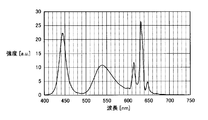
- FIG. 2 shows a specific example of a divalent europium-activated oxynitride green light-emitting phosphor that is a ⁇ -type SiAlON that can be used in the light-emitting device of the present invention (specific composition: Eu 0.05 Si 11.50 Al 0.50 O 0.05 N 15.95) emission spectrum distribution of FIG. 3, one specific example of the divalent europium-activated silicate phosphors that may be used in the light-emitting device of the present invention (specific composition: 2 (Ba 0.70 Sr 0.26 Eu 0.04 ) O ⁇ SiO 2 ) emission spectrum distribution, FIG.
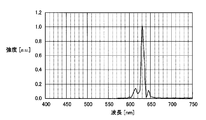
- FIG. 4 shows a specific example of a tetravalent manganese-activated fluorinated tetravalent metal salt phosphor that can be used in the light-emitting device of the present invention (specifically The emission spectrum distribution of composition: K 2 (Ti 0.99 Mn 0.01 ) F 6 ) is shown. All emission spectra shown in FIG. 2 to FIG. 4 are the results of measurement with an excitation wavelength of 450 nm using a fluorescence spectrophotometer, the vertical axis is intensity (arbitrary unit), and the horizontal axis is wavelength (nm). .
- the mixing ratio of the green light emitting phosphor and the red light emitting phosphor is not particularly limited, but the green light emitting phosphor is 5 to 70% by weight with respect to the red light emitting phosphor. Mixing at a mixing ratio within the range is preferable, and mixing at a mixing ratio within the range of 15 to 45% is more preferable.
- FIG. 5 is a graph showing the emission spectrum distribution of a preferred example of the light-emitting device of the present invention (the light-emitting device produced in Example 1 described later).
- the vertical axis represents intensity (arbitrary unit), horizontal
- the axis is the wavelength (nm).
- FIG. 6 is a chromaticity diagram (CIE1931) showing the color reproducibility of an LCD in which a light emitting device of a preferred example of the present invention (light emitting device manufactured in Example 1 described later) is incorporated as a backlight light source.
- FIG. 10 chromaticity diagram
- FIG. 7 is a graph showing an emission spectrum distribution of a conventional light-emitting device using a yellow light-emitting phosphor (light-emitting device manufactured in Comparative Example 1 described later), and FIG. It is a chromaticity diagram (CIE1931) showing the color reproducibility of an LCD incorporated as a backlight light source.
- the emission spectrum distribution of the light emitting device shown in FIGS. 5 and 7 is a result of measurement using MCPD-2000 (manufactured by Otsuka Electronics Co., Ltd.), and the color reproducibility shown in FIGS. 6 and 8 is used. These are the results measured using Bm5 (Topcon Co., Ltd.). From FIG. 5 to FIG.
- the light from the light emitting element is efficiently absorbed in the wavelength conversion unit to emit highly efficient white light, It can be seen that a light-emitting device capable of obtaining white light with remarkably good color reproducibility (NTSC ratio) is provided.
- the NTSC ratio refers to the red, green, blue, and chromaticity coordinates (x, y) in the XYZ color system chromaticity diagram defined by NTSC (National Television System Committee) for red (0.670, 0). .330), green (0.210, 0.710), and blue (0.140, 0.080), and the ratio to the area of the triangle obtained by connecting the chromaticity coordinates of red, green, and blue respectively. Represents.
- the light-emitting element used in the above-described light-emitting device of the present invention is not particularly limited, but gallium nitride (GaN) that emits primary light in a blue region having a peak wavelength of 430 to 480 nm (more preferably 440 to 480 nm).
- GaN gallium nitride
- Based semiconductors can be suitably used as light emitting elements. This is because when a light-emitting element having a peak wavelength of less than 430 nm is used, the contribution of the blue light component is reduced, color rendering becomes worse, and may not be practical, and light emission with a peak wavelength exceeding 480 nm. This is because when the element is used, the brightness in white is lowered, which may be impractical.
- the light emitting device of the present invention has the above-described features, other configurations are not particularly limited.
- the sealant 6 an epoxy resin, a silicone resin, a urea resin, or the like, which is a light-transmitting resin material, can be used, but is not limited thereto.
- the wavelength conversion unit 3 may have any appropriate SiO 2 , TiO 2 , ZrO 2 , Al 2 O 3 , Y 2 O 3 as long as the effects of the present invention are not impaired. Of course, additives such as may be contained.
- green light-emitting phosphor and red light-emitting phosphor used in the light-emitting device of the present invention are both known, and are manufactured by a conventionally known appropriate method or obtained as a product. Is possible.
- the light emitting device 1 of the example shown in FIG. 1 was produced as follows.
- a gallium nitride (GaN) -based semiconductor having a peak wavelength at 450 nm is used as the light-emitting element 2
- the wavelength conversion unit 3 includes Eu 0.05 Si 11.50 Al 0.50 O 0.05 N 15.95 ( ⁇ -type SiAlON) as a green light-emitting phosphor.
- K 2 (Ti 0.99 Mn 0.01 ) F 6 was used as the red light emitting phosphor.
- Example 1 A light emitting device was fabricated in the same manner as in Example 1 except that a yellow light emitting phosphor represented by (Y 0.40 Gd 0.45 Ce 0.15 ) 3 Al 5 O 12 was used for the wavelength conversion section.
- a yellow light emitting phosphor represented by (Y 0.40 Gd 0.45 Ce 0.15 ) 3 Al 5 O 12 was used for the wavelength conversion section.
- the light-emitting devices obtained in Example 1 and Comparative Example 1 were evaluated for brightness, Tc-duv, and color reproducibility (NTSC ratio).
- the brightness was determined by turning on the light at a forward current (IF) of 20 mA and converting white light from the light emitting device into a photocurrent. Further, Tc-duv was turned on under the condition of forward current (IF) 20 mA, and white light from the light emitting device was measured with MCPD-2000 manufactured by Otsuka Electronics Co., Ltd., and the value was obtained.
- the color reproducibility (NTSC ratio) was determined by incorporating the produced light-emitting device as a backlight light source of a commercially available LCD TV display and measuring it with Bm5 manufactured by Topcon Corporation. The results are shown in Table 1.
- the light-emitting device of the present invention has dramatically improved color reproducibility (NTSC ratio) compared to conventional products, and has characteristics suitable as a backlight for medium and small LCDs. I understand.
- Example 2 A gallium nitride (GaN) -based semiconductor having a peak wavelength of 440 nm is used as the light-emitting element 2, 2 (Ba 0.70 Sr 0.26 Eu 0.04 ) O ⁇ SiO 2 as a green light-emitting phosphor, and K as a red light-emitting phosphor.
- GaN gallium nitride
- a light emitting device was fabricated in the same manner as in Example 1 except that 2 (Ti 0.995 Mn 0.005 ) F 6 was used.
- Example 2 A light emitting device was fabricated in the same manner as in Example 2 except that a yellow light emitting phosphor represented by (Y 0.40 Gd 0.50 Ce 0.10 ) 3 Al 5 O 12 was used for the wavelength conversion unit.
- a yellow light emitting phosphor represented by (Y 0.40 Gd 0.50 Ce 0.10 ) 3 Al 5 O 12 was used for the wavelength conversion unit.
- Example 2 and Comparative Example 2 were also evaluated for brightness, Tc-duv, and color reproducibility (NTSC ratio) in the same manner as the light emitting devices of Example 1 and Comparative Example 1 described above. did. The results are shown in Table 2.
- the light emitting device of the present invention has dramatically improved color reproducibility (NTSC ratio) compared to conventional products, and has characteristics suitable as a backlight for medium and small LCDs. I understand.
- Examples 3 to 8 Comparative Examples 3 to 8>
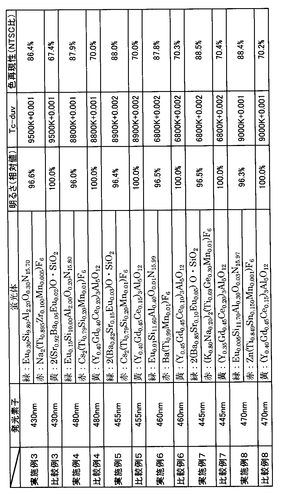
- the light emitting devices of Examples 3 to 8 and Comparative Examples 3 to 8 were produced in the same manner as in Example 1 except that the combinations of the peak wavelengths of the light emitting elements and the phosphors shown in Table 3 below were used, respectively.
- the brightness, Tc-duv, and color reproducibility (NTSC ratio) were evaluated in the same manner as described above. The results are also shown in Table 3.
- Table 3 also shows that the light emitting device of the present invention has drastically improved color reproducibility (NTSC ratio) compared to conventional products, and has characteristics suitable as a backlight for medium and small LCDs. I understand.
Landscapes
- Chemical & Material Sciences (AREA)
- Physics & Mathematics (AREA)
- Inorganic Chemistry (AREA)
- Engineering & Computer Science (AREA)
- Materials Engineering (AREA)
- Organic Chemistry (AREA)
- Nonlinear Science (AREA)
- Mathematical Physics (AREA)
- Crystallography & Structural Chemistry (AREA)
- General Physics & Mathematics (AREA)
- Optics & Photonics (AREA)
- Luminescent Compositions (AREA)
- Led Device Packages (AREA)
Abstract
Description
一般式(A):EuaSibAlcOdNe
(上記一般式(A)中、0.005≦a≦0.4、b+c=12、d+e=16である。)で実質的に表されるβ型SiAlONである2価のユーロピウム付活酸窒化物蛍光体、ならびに、
一般式(B):2(Ba1-f-gMIfEug)O・SiO2
(上記一般式(B)中、MIはMg、CaおよびSrから選らばれる少なくとも1種のアルカリ土類金属元素を示し、0<f≦0.55、0.03≦g≦0.10である。)で実質的に表される2価のユーロピウム付活珪酸塩蛍光体から選ばれる少なくとも1種からなり、上記赤色系発光蛍光体が、
一般式(C):MII2(MIII1-hMnh)F6
(上記一般式(C)中、MIIはLi、Na、K、RbおよびCsから選ばれる少なくとも1種のアルカリ金属元素、MIIIはGe、Si、Sn、TiおよびZrから選ばれる少なくとも1種の4価の金属元素を示し、0.001≦h≦0.1である。)で実質的に表される4価のマンガン付活フッ化4価金属塩蛍光体、ならびに、
一般式(D):MIV(MIII1-hMnh)F6
(上記一般式(D)中、MIVはMg、Ca、Sr、BaおよびZnから選ばれる少なくとも1種のアルカリ土類金属元素、MIIIはGe、Si、Sn、TiおよびZrから選ばれる少なくとも1種の4価の金属元素を示し、0.001≦h≦0.1である。)で実質的に表される4価のマンガン付活フッ化4価金属塩蛍光体から選ばれる少なくとも1種からなることを特徴とする。
また本発明の発光装置において、0.005≦h≦0.05であることが好ましい。
本発明の発光装置における発光素子は、ピーク波長430~480nmの一次光を発する窒化ガリウム系半導体であることが好ましい。
当該2価のユーロピウム付活酸窒化物緑色系発光蛍光体は、
一般式(A):EuaSibAlcOdNe
で実質的に表される(以下、当該2価のユーロピウム付活酸窒化物緑色系発光蛍光体を「第1の緑色系発光蛍光体」と呼称する。)。一般式(A)において、Euはユーロピウム、Siはケイ素、Alはアルミニウム、Oは酸素、Nは窒素を表している。一般式(A)中、Euの組成比(濃度)を表すaの値は0.005≦a≦0.4である。aの値が0.005未満である場合には、十分な明るさが得られないためであり、またaの値が0.4を超える場合には、濃度消光などにより、明るさが大きく低下するためである。なお、粉体特性の安定性、母体の均質性から、上記式中のaの値は、0.01≦a≦0.2であるのが好ましい。また、一般式(A)において、Siの組成比(濃度)を表すbおよびAlの組成比(濃度)を表すcは、b+c=12を満足する数であり、Oの組成比(濃度)を表すdおよびNの組成比(濃度)を表すeは、d+e=16を満足する数である。
当該2価のユーロピウム付活珪酸塩蛍光体は、
一般式(B):2(Ba1-f-gMIfEug)O・SiO2
で実質的に表される(以下、当該2価のユーロピウム付活珪酸塩蛍光体を「第2の緑色系発光蛍光体」と呼称する。)。一般式(B)において、Baはバリウム、Euはユーロピウム、Oは酸素、Siはケイ素を表している。一般式(B)中、MIは、Mg、CaおよびSrから選ばれる少なくとも1種のアルカリ土類金属元素を示し、高効率な母体を得るためには、MIはSrであることが好ましい。一般式(B)中、MIの組成比(濃度)を表すfの値は0<f≦0.55であり、fの値がこの範囲内であることで、510~540nmの範囲の緑色系発光を得ることができる。fの値が0.55を超える場合には、黄色味がかった緑色系発光となり、色純度が悪くなってしまう。さらには、効率、色純度の観点からは、fの値は0.15≦f≦0.45の範囲の範囲内であることが好ましい。また一般式(B)中、Euの組成比(濃度)を示すgの値は0.03≦g≦0.10である。gの値が0.03未満である場合には、十分な明るさが得られないためであり、また、gの値が0.10を超える場合には、濃度消光などにより、明るさが大きく低下するためである。なお、明るさおよび粉体特性の安定性から、gの値は0.04≦g≦0.08の範囲内であることが好ましい。
当該4価のマンガン付活フッ化4価金属塩蛍光体は、
一般式(C):MII2(MIII1-hMnh)F6
で実質的に表される(以下、当該4価のマンガン付活フッ化4価金属塩蛍光体を「第1の赤色系発光蛍光体」と呼称する。)。なお、一般式(C)において、Mnはマンガン、Fはフッ素を表している。一般式(C)中、MIIは、Na、K、RbおよびCsから選ばれる少なくとも1種のアルカリ金属元素を示し、明るさおよび粉体特性の安定性から、MIIはKであることが好ましい。また一般式(C)中、MIIIは、Ge、Si、Sn、TiおよびZrから選ばれる少なくとも1種の4価の金属元素を示し、明るさおよび粉体特性の安定性から、MIIIはTiであることが好ましい。また、一般式(C)中、Mnの組成比(濃度)を示すhの値は0.001≦h≦0.1である。hの値が0.001未満である場合には、十分な明るさが得られないという不具合があり、また、hの値が0.1を超える場合には、濃度消光などにより、明るさが大きく低下するという不具合があるためである。明るさおよび粉体特性の安定性から、hの値は0.005≦h≦0.5であることが好ましい。
当該4価のマンガン付活フッ化4価金属塩蛍光体は、
一般式(D):MIV(MIII1-hMnh)F6
で実質的に表される(以下、当該4価のマンガン付活フッ化4価金属塩蛍光体を「第2の赤色系発光蛍光体」と呼称する。)。なお、一般式(D)において、Mnはマンガン、Fはフッ素を表している。一般式(D)中、MIIIは、上述した一般式(C)中のMIIIと同じくGe、Si、Sn、TiおよびZrから選ばれる少なくとも1種の4価の金属元素を示し、同様の理由から、MIIIはTiであることが好ましい。また一般式(D)中、MIVは、Mg、Ca、Sr、BaおよびZnから選ばれる少なくとも1種のアルカリ土類金属元素を示し、明るさおよび粉体特性の安定性から、MIVはCaであることが好ましい。また、一般式(D)中、Mnの組成比(濃度)を示すhの値は、上述した一般式(C)中のhと同じく0.001≦h≦0.1であり、同様の理由から、0.005≦h≦0.5であることが好ましい。
以下のようにして図1に示した例の発光装置1を作製した。発光素子2として、450nmにピーク波長を有する窒化ガリウム(GaN)系半導体を用い、波長変換部3には、緑色系発光蛍光体としてEu0.05Si11.50Al0.50O0.05N15.95(β型SiAlON)、赤色系発光蛍光体としてK2(Ti0.99Mn0.01)F6を用いた。これらの緑色系発光蛍光体と赤色系発光蛍光体とを30:70の割合(重量比)で混合したものを所定の樹脂中に分散し(樹脂と蛍光体との比率は1.00:0.25)、波長変換部を作製した。このようにして実施例1の発光装置を作製した。
(Y0.40Gd0.45Ce0.15)3Al5O12で表される黄色系発光蛍光体を波長変換部に用いたこと以外は実施例1と同様にして発光装置を作製した。

発光素子2として440nmにピ-ク波長を有する窒化ガリウム(GaN)系半導体を用いた、緑色系発光蛍光体として2(Ba0.70Sr0.26Eu0.04)O・SiO2、赤色系発光蛍光体としてK2(Ti0.995Mn0.005)F6を用いたこと以外は実施例1と同様にして発光装置を作製した。
(Y0.40Gd0.50Ce0.10)3Al5O12で表される黄色系発光蛍光体を波長変換部に用いたこと以外は実施例2と同様にして発光装置を作製した。

下記の表3に示すような発光素子のピーク波長および蛍光体の組み合わせをそれぞれ用いたこと以外は実施例1と同様にして実施例3~8および比較例3~8の発光装置を作製し、上述と同様にして明るさ、Tc-duvおよび色再現性(NTSC比)を評価した。結果も併せて表3に示す。
Claims (5)
- 一次光を発する発光素子(2)と、発光素子(2)から発せられた一次光の一部を吸収して、一次光の波長よりも長い波長を有する二次光を発する波長変換部(3)とを備える発光装置(1)であって、上記波長変換部(3)は、緑色系発光蛍光体(4)および赤色発光蛍光体(5)を含み、
上記緑色系発光蛍光体(4)が、
一般式(A):EuaSibAlcOdNe
(上記一般式(A)中、0.005≦a≦0.4、b+c=12、d+e=16である。)
で実質的に表されるβ型SiAlONである2価のユーロピウム付活酸窒化物蛍光体、ならびに、
一般式(B):2(Ba1-f-gMIfEug)O・SiO2
(上記一般式(B)中、MIはMg、CaおよびSrから選らばれる少なくとも1種のアルカリ土類金属元素を示し、0<f≦0.55、0.03≦g≦0.10である。)
で実質的に表される2価のユーロピウム付活珪酸塩蛍光体から選ばれる少なくとも1種からなり、
上記赤色系発光蛍光体(5)が、
一般式(C):MII2(MIII1-hMnh)F6
(上記一般式(C)中、MIIはLi、Na、K、RbおよびCsから選ばれる少なくとも1種のアルカリ金属元素、MIIIはGe、Si、Sn、TiおよびZrから選ばれる少なくとも1種の4価の金属元素を示し、0.001≦h≦0.1である。)
で実質的に表される4価のマンガン付活フッ化4価金属塩蛍光体、ならびに、
一般式(D):MIV(MIII1-hMnh)F6
(上記一般式(D)中、MIVはMg、Ca、Sr、BaおよびZnから選ばれる少なくとも1種のアルカリ土類金属元素、MIIIはGe、Si、Sn、TiおよびZrから選ばれる少なくとも1種の4価の金属元素を示し、0.001≦h≦0.1である。)
で実質的に表される4価のマンガン付活フッ化4価金属塩蛍光体から選ばれる少なくとも1種からなる、発光装置(1)。 - MIIはKであり、MIIIはTiである、請求の範囲第1項に記載の発光装置(1)。
- 0.005≦h≦0.05である、請求の範囲第1項に記載の発光装置(1)。
- MIはSrである、請求の範囲第1項に記載の発光装置(1)。
- 発光素子(2)が、ピーク波長430~480nmの一次光を発する窒化ガリウム系半導体である、請求の範囲第1項に記載の発光装置(1)。
Priority Applications (8)
| Application Number | Priority Date | Filing Date | Title |
|---|---|---|---|
| JP2010501831A JPWO2009110285A1 (ja) | 2008-03-03 | 2009-02-06 | 発光装置 |
| CN2009801076946A CN101960624B (zh) | 2008-03-03 | 2009-02-06 | 发光装置 |
| US12/920,516 US8237348B2 (en) | 2008-03-03 | 2009-02-06 | Light-emitting device |
| US13/542,051 US8362685B2 (en) | 2008-03-03 | 2012-07-05 | Light-emitting device |
| US13/729,191 US8829781B2 (en) | 2008-03-03 | 2012-12-28 | Light-emitting device |
| US14/470,153 US8981639B2 (en) | 2008-03-03 | 2014-08-27 | Light-emitting device |
| US14/615,017 US9184353B2 (en) | 2008-03-03 | 2015-02-05 | Light-emitting device |
| US14/936,037 US9455381B2 (en) | 2008-03-03 | 2015-11-09 | Light-emitting device |
Applications Claiming Priority (2)
| Application Number | Priority Date | Filing Date | Title |
|---|---|---|---|
| JP2008052210 | 2008-03-03 | ||
| JP2008-052210 | 2008-03-03 |
Related Child Applications (2)
| Application Number | Title | Priority Date | Filing Date |
|---|---|---|---|
| US12/920,516 A-371-Of-International US8237348B2 (en) | 2008-03-03 | 2009-02-06 | Light-emitting device |
| US13/542,051 Continuation US8362685B2 (en) | 2008-03-03 | 2012-07-05 | Light-emitting device |
Publications (1)
| Publication Number | Publication Date |
|---|---|
| WO2009110285A1 true WO2009110285A1 (ja) | 2009-09-11 |
Family
ID=41055846
Family Applications (1)
| Application Number | Title | Priority Date | Filing Date |
|---|---|---|---|
| PCT/JP2009/052051 Ceased WO2009110285A1 (ja) | 2008-03-03 | 2009-02-06 | 発光装置 |
Country Status (5)
| Country | Link |
|---|---|
| US (6) | US8237348B2 (ja) |
| JP (2) | JPWO2009110285A1 (ja) |
| CN (2) | CN102790164B (ja) |
| TW (3) | TWI456789B (ja) |
| WO (1) | WO2009110285A1 (ja) |
Cited By (18)
| Publication number | Priority date | Publication date | Assignee | Title |
|---|---|---|---|---|
| US8491816B2 (en) | 2008-02-07 | 2013-07-23 | Mitsubishi Chemical Corporation | Semiconductor light emitting device, backlight, color image display device and phosphor to be used for them |
| WO2014104152A1 (ja) | 2012-12-28 | 2014-07-03 | 信越化学工業株式会社 | 発光装置 |
| WO2014203841A1 (ja) * | 2013-06-18 | 2014-12-24 | シャープ株式会社 | 発光装置 |
| WO2015025743A1 (ja) * | 2013-08-23 | 2015-02-26 | シャープ株式会社 | 液晶表示装置 |
| JP2015087527A (ja) * | 2013-10-30 | 2015-05-07 | 大日本印刷株式会社 | 高色域液晶表示装置 |
| EP2650934A4 (en) * | 2010-12-09 | 2016-02-24 | Sharp Kk | Light-emitting device |
| KR20160104681A (ko) | 2014-01-28 | 2016-09-05 | 샤프 가부시키가이샤 | 발광 다이오드 구동 장치 및 조명 장치 |
| KR20160138901A (ko) | 2015-05-26 | 2016-12-06 | 샤프 가부시키가이샤 | 발광 장치 및 화상 표시 장치 |
| JP2016207817A (ja) * | 2015-04-21 | 2016-12-08 | シャープ株式会社 | 発光装置および画像表示装置 |
| JP2017500732A (ja) * | 2013-11-06 | 2017-01-05 | ゼネラル・エレクトリック・カンパニイ | 赤色発光蛍光体を有するledパッケージ |
| US9614130B2 (en) | 2013-11-08 | 2017-04-04 | Sharp Kabushiki Kaisha | Light emitting device and illumination device |
| US9944848B2 (en) | 2014-09-30 | 2018-04-17 | Nichia Corporation | Fluoride fluorescent material, method for producing the same, and light emitting device |
| KR20180096502A (ko) | 2017-02-21 | 2018-08-29 | 샤프 가부시키가이샤 | 발광 장치 및 화상 표시 장치 |
| JP2019029584A (ja) * | 2017-08-02 | 2019-02-21 | シャープ株式会社 | 発光装置及び画像表示装置 |
| JP2019033260A (ja) * | 2014-03-14 | 2019-02-28 | 日亜化学工業株式会社 | 発光装置 |
| US10381528B2 (en) | 2015-08-31 | 2019-08-13 | Sharp Kabushiki Kaisha | Image display apparatus |
| US10381529B2 (en) | 2016-03-28 | 2019-08-13 | Sharp Kabushiki Kaisha | Light-emitting device and display device |
| JP2019165257A (ja) * | 2017-01-13 | 2019-09-26 | 日亜化学工業株式会社 | 発光装置 |
Families Citing this family (48)
| Publication number | Priority date | Publication date | Assignee | Title |
|---|---|---|---|---|
| US8214741B2 (en) | 2002-03-19 | 2012-07-03 | Sharp Laboratories Of America, Inc. | Synchronization of video and data |
| JP5367218B2 (ja) | 2006-11-24 | 2013-12-11 | シャープ株式会社 | 蛍光体の製造方法および発光装置の製造方法 |
| CN102790164B (zh) | 2008-03-03 | 2016-08-10 | Ge磷光体技术有限责任公司 | 发光装置 |
| US8703016B2 (en) | 2008-10-22 | 2014-04-22 | General Electric Company | Phosphor materials and related devices |
| TWI592465B (zh) * | 2010-11-22 | 2017-07-21 | 宇部興產股份有限公司 | Silicate phosphor and light-emitting device having high light-emitting property and moisture resistance |
| CN102250611B (zh) * | 2011-07-26 | 2013-09-11 | 彩虹集团公司 | 一种硅酸盐绿色荧光粉及其制备方法 |
| US9082349B2 (en) * | 2011-08-30 | 2015-07-14 | Sharp Laboratories Of America, Inc. | Multi-primary display with active backlight |
| US10310363B2 (en) | 2011-09-22 | 2019-06-04 | Delta Electronics, Inc. | Phosphor device with spectrum of converted light comprising at least a color light |
| TWI448806B (zh) | 2011-09-22 | 2014-08-11 | Delta Electronics Inc | 螢光劑裝置及其所適用之光源系統及投影設備 |
| US10688527B2 (en) | 2011-09-22 | 2020-06-23 | Delta Electronics, Inc. | Phosphor device comprising plural phosphor agents for converting waveband light into plural color lights with different wavelength peaks |
| JP2013201274A (ja) * | 2012-03-23 | 2013-10-03 | Toshiba Lighting & Technology Corp | 照明装置 |
| DE102012105208A1 (de) * | 2012-06-15 | 2013-12-19 | Osram Opto Semiconductors Gmbh | Halbleiterlichtquelle |
| CN104871325A (zh) * | 2012-12-28 | 2015-08-26 | 信越化学工业株式会社 | 调整部件和发光装置 |
| US9580648B2 (en) | 2013-03-15 | 2017-02-28 | General Electric Company | Color stable red-emitting phosphors |
| US9698314B2 (en) | 2013-03-15 | 2017-07-04 | General Electric Company | Color stable red-emitting phosphors |
| US9399732B2 (en) | 2013-08-22 | 2016-07-26 | General Electric Company | Processes for preparing color stable manganese-doped phosphors |
| US11041118B2 (en) | 2013-08-29 | 2021-06-22 | Nichia Corporation | Fluoride fluorescent material and method for producing the same as well as light emitting device using the same |
| JP6201665B2 (ja) * | 2013-11-13 | 2017-09-27 | 日亜化学工業株式会社 | 画像表示装置の製造方法並びに発光装置及びカラーフィルターの選択方法 |
| CN105793389B (zh) | 2013-12-13 | 2018-12-04 | 通用电气公司 | 制备颜色稳定的锰掺杂的络合氟化物磷光体的方法 |
| WO2015098814A1 (ja) | 2013-12-26 | 2015-07-02 | 電気化学工業株式会社 | 蛍光体及び発光装置 |
| KR102331836B1 (ko) | 2014-02-26 | 2021-11-26 | 덴카 주식회사 | 형광체, 발광 소자 및 발광 장치 |
| US9680066B2 (en) | 2014-02-26 | 2017-06-13 | Denka Company Limited | Phosphor, light emitting element, and light emitting device |
| US10230022B2 (en) | 2014-03-13 | 2019-03-12 | General Electric Company | Lighting apparatus including color stable red emitting phosphors and quantum dots |
| JP6187509B2 (ja) * | 2014-03-14 | 2017-08-30 | 日亜化学工業株式会社 | 発光装置及びその製造方法 |
| US9755116B2 (en) | 2014-03-14 | 2017-09-05 | Nichia Corporation | Method of manufacturing light emitting device |
| KR102164079B1 (ko) | 2014-05-30 | 2020-10-12 | 엘지이노텍 주식회사 | 산질화물계 형광체를 포함하는 발광 소자 패키지 |
| US9371481B2 (en) | 2014-06-12 | 2016-06-21 | General Electric Company | Color stable red-emitting phosphors |
| US9567516B2 (en) | 2014-06-12 | 2017-02-14 | General Electric Company | Red-emitting phosphors and associated devices |
| US9376615B2 (en) | 2014-06-12 | 2016-06-28 | General Electric Company | Color stable red-emitting phosphors |
| US9385282B2 (en) | 2014-06-12 | 2016-07-05 | General Electric Company | Color stable red-emitting phosphors |
| US9929319B2 (en) | 2014-06-13 | 2018-03-27 | General Electric Company | LED package with red-emitting phosphors |
| WO2016056485A1 (ja) * | 2014-10-10 | 2016-04-14 | シャープ株式会社 | 液晶表示装置 |
| US10047286B2 (en) | 2014-10-27 | 2018-08-14 | General Electric Company | Color stable red-emitting phosphors |
| KR102355081B1 (ko) | 2014-12-26 | 2022-01-26 | 삼성전자주식회사 | 불화물 형광체 제조방법, 백색 발광장치, 디스플레이 장치 및 조명장치 |
| US9982190B2 (en) | 2015-02-20 | 2018-05-29 | General Electric Company | Color stable red-emitting phosphors |
| CN106281320A (zh) | 2015-05-21 | 2017-01-04 | 隆达电子股份有限公司 | 荧光粉、其制备方法及包含其发光装置与背光模块 |
| CN106244143B (zh) | 2015-06-04 | 2019-08-27 | 隆达电子股份有限公司 | 具有优选方向的荧光粉、其制备方法及包含其的发光元件封装结构 |
| DE102016111384A1 (de) * | 2015-06-29 | 2016-12-29 | Ford Global Technologies, Llc | Photolumineszierende Windenvorrichtung |
| TWI564367B (zh) | 2015-11-16 | 2017-01-01 | 隆達電子股份有限公司 | 氟化物螢光粉、其製備方法及包含其之發光裝置與背光模組 |
| CN108351444B (zh) * | 2015-12-04 | 2021-10-26 | 东丽株式会社 | 荧光体片、使用其的发光体、光源单元、显示器及发光体的制造方法 |
| TWI618946B (zh) * | 2015-12-22 | 2018-03-21 | Delta Electronics, Inc. | 螢光劑裝置及其製造方法 |
| TWI575058B (zh) | 2016-01-06 | 2017-03-21 | 隆達電子股份有限公司 | 螢光粉、其製備方法、調控其晶相的方法、及使其產生相轉變的方法 |
| US11114591B2 (en) | 2016-08-17 | 2021-09-07 | Current Lighting Solutions, Llc | Core-shell materials with red-emitting phosphors |
| TWI652329B (zh) | 2016-10-19 | 2019-03-01 | 隆達電子股份有限公司 | 含有片狀結晶體之氟化物螢光粉及其製造方法與應用 |
| TWI615458B (zh) | 2016-10-28 | 2018-02-21 | 隆達電子股份有限公司 | 波長轉換膜片及應用其之發光裝置與顯示器 |
| CN110476112B (zh) * | 2017-03-30 | 2022-07-19 | 夏普株式会社 | 显示装置和头戴显示器 |
| US10177287B1 (en) * | 2017-09-19 | 2019-01-08 | Eie Materials, Inc. | Gamut broadened displays with narrow band green phosphors |
| WO2021185756A1 (de) * | 2020-03-16 | 2021-09-23 | Osram Opto Semiconductors Gmbh | Leuchtstoff, verfahren zur herstellung eines leuchtstoffs und strahlungsemittierendes bauelement |
Citations (4)
| Publication number | Priority date | Publication date | Assignee | Title |
|---|---|---|---|---|
| US20060169998A1 (en) * | 2005-02-02 | 2006-08-03 | Gelcore, Llc | Red line emitting phosphor materials for use in LED applications |
| JP2006524425A (ja) * | 2003-04-25 | 2006-10-26 | ルクスピア カンパニー リミテッド | 白色半導体発光装置 |
| WO2007066733A1 (ja) * | 2005-12-08 | 2007-06-14 | National Institute For Materials Science | 蛍光体とその製造方法および発光器具 |
| JP2008021868A (ja) * | 2006-07-13 | 2008-01-31 | Nippon Electric Glass Co Ltd | 蛍光体複合部材 |
Family Cites Families (31)
| Publication number | Priority date | Publication date | Assignee | Title |
|---|---|---|---|---|
| US6016A (en) * | 1849-01-09 | Improvement in corn-planters | ||
| US6252254B1 (en) * | 1998-02-06 | 2001-06-26 | General Electric Company | Light emitting device with phosphor composition |
| JP2003121838A (ja) | 2001-08-06 | 2003-04-23 | Toray Ind Inc | 液晶表示装置 |
| AU2003215785A1 (en) | 2002-03-25 | 2003-10-08 | Philips Intellectual Property And Standards Gmbh | Tri-color white light led lamp |
| JP4053926B2 (ja) | 2002-05-27 | 2008-02-27 | 日亜化学工業株式会社 | 窒化物半導体発光素子とそれを用いた発光装置 |
| DE60325851D1 (de) * | 2002-06-13 | 2009-03-05 | Cree Inc | Halbleiter-strahlungsquelle mit gesättigtem phosphor |
| JP4124684B2 (ja) | 2003-03-25 | 2008-07-23 | セイコーインスツル株式会社 | 半透過型液晶表示装置 |
| JP3921545B2 (ja) | 2004-03-12 | 2007-05-30 | 独立行政法人物質・材料研究機構 | 蛍光体とその製造方法 |
| KR100887489B1 (ko) | 2004-04-27 | 2009-03-10 | 파나소닉 주식회사 | 형광체 조성물과 그 제조 방법, 및 그 형광체 조성물을이용한 발광 장치 |
| JP4128564B2 (ja) | 2004-04-27 | 2008-07-30 | 松下電器産業株式会社 | 発光装置 |
| EP1790199B1 (en) | 2004-06-29 | 2013-08-14 | Panasonic Corporation | Illumination source |
| JP2006083219A (ja) | 2004-09-14 | 2006-03-30 | Sharp Corp | 蛍光体およびこれを用いた発光装置 |
| WO2006033239A1 (ja) * | 2004-09-22 | 2006-03-30 | Kabushiki Kaisha Toshiba | 発光装置とそれを用いたバックライトおよび液晶表示装置 |
| JP4635551B2 (ja) | 2004-10-06 | 2011-02-23 | ソニー株式会社 | カラー液晶表示装置 |
| JP2006165266A (ja) * | 2004-12-07 | 2006-06-22 | Matsushita Electric Works Ltd | 発光装置 |
| US7648649B2 (en) | 2005-02-02 | 2010-01-19 | Lumination Llc | Red line emitting phosphors for use in led applications |
| US7358542B2 (en) | 2005-02-02 | 2008-04-15 | Lumination Llc | Red emitting phosphor materials for use in LED and LCD applications |
| US20070114562A1 (en) | 2005-11-22 | 2007-05-24 | Gelcore, Llc | Red and yellow phosphor-converted LEDs for signal applications |
| JP2006261600A (ja) | 2005-03-18 | 2006-09-28 | Matsushita Electric Ind Co Ltd | 照明モジュール、照明装置及び照明モジュールの製造方法 |
| JP2007027421A (ja) | 2005-07-15 | 2007-02-01 | Harison Toshiba Lighting Corp | Ledパッケージ及び照明装置 |
| JP2007088300A (ja) | 2005-09-22 | 2007-04-05 | Mitsubishi Chemicals Corp | 発光装置並びに照明装置及び画像表示装置 |
| JP4769132B2 (ja) | 2005-11-30 | 2011-09-07 | シャープ株式会社 | 発光装置 |
| JP4971630B2 (ja) * | 2005-12-21 | 2012-07-11 | Dowaホールディングス株式会社 | 蛍光体およびその製造方法、並びに発光装置 |
| TW200801158A (en) | 2006-02-02 | 2008-01-01 | Mitsubishi Chem Corp | Complex oxynitride phosphor, light-emitting device using the same, image display, illuminating device, phosphor-containing composition and complex oxynitride |
| KR100735453B1 (ko) * | 2006-02-22 | 2007-07-04 | 삼성전기주식회사 | 백색 발광 장치 |
| KR100875443B1 (ko) | 2006-03-31 | 2008-12-23 | 서울반도체 주식회사 | 발광 장치 |
| TWI357927B (en) | 2006-11-20 | 2012-02-11 | Denki Kagaku Kogyo Kk | Fluorescent substance and manufacturing method the |
| CN102790164B (zh) | 2008-03-03 | 2016-08-10 | Ge磷光体技术有限责任公司 | 发光装置 |
| JP2009280763A (ja) | 2008-05-26 | 2009-12-03 | Sharp Corp | 蛍光体調製物およびそれを用いた発光装置 |
| CN102656248B (zh) | 2010-01-08 | 2014-07-16 | 夏普株式会社 | 荧光体、发光装置及使用它的液晶显示装置 |
| JP4740379B1 (ja) | 2010-02-25 | 2011-08-03 | 電気化学工業株式会社 | β型サイアロン蛍光体、その用途及びβ型サイアロン蛍光体の製造方法 |
-
2009
- 2009-02-06 CN CN201210286813.2A patent/CN102790164B/zh active Active
- 2009-02-06 WO PCT/JP2009/052051 patent/WO2009110285A1/ja not_active Ceased
- 2009-02-06 JP JP2010501831A patent/JPWO2009110285A1/ja active Pending
- 2009-02-06 US US12/920,516 patent/US8237348B2/en active Active
- 2009-02-06 CN CN2009801076946A patent/CN101960624B/zh active Active
- 2009-02-12 TW TW098104537A patent/TWI456789B/zh active
- 2009-02-12 TW TW106132825A patent/TWI655789B/zh active
- 2009-02-12 TW TW103122432A patent/TWI615995B/zh active
-
2012
- 2012-07-05 US US13/542,051 patent/US8362685B2/en active Active
- 2012-12-28 US US13/729,191 patent/US8829781B2/en active Active
-
2013
- 2013-09-27 JP JP2013201611A patent/JP2014039052A/ja active Pending
-
2014
- 2014-08-27 US US14/470,153 patent/US8981639B2/en active Active
-
2015
- 2015-02-05 US US14/615,017 patent/US9184353B2/en active Active
- 2015-11-09 US US14/936,037 patent/US9455381B2/en active Active
Patent Citations (4)
| Publication number | Priority date | Publication date | Assignee | Title |
|---|---|---|---|---|
| JP2006524425A (ja) * | 2003-04-25 | 2006-10-26 | ルクスピア カンパニー リミテッド | 白色半導体発光装置 |
| US20060169998A1 (en) * | 2005-02-02 | 2006-08-03 | Gelcore, Llc | Red line emitting phosphor materials for use in LED applications |
| WO2007066733A1 (ja) * | 2005-12-08 | 2007-06-14 | National Institute For Materials Science | 蛍光体とその製造方法および発光器具 |
| JP2008021868A (ja) * | 2006-07-13 | 2008-01-31 | Nippon Electric Glass Co Ltd | 蛍光体複合部材 |
Cited By (36)
| Publication number | Priority date | Publication date | Assignee | Title |
|---|---|---|---|---|
| US12084609B2 (en) | 2008-02-07 | 2024-09-10 | Citizen Electronics Co., Ltd. | Light emitting device |
| US10011769B2 (en) | 2008-02-07 | 2018-07-03 | Mitsubishi Chemical Corporation | Semiconductor light emitting device, backlight, color image display device and phosphor to be used for them |
| US10858582B2 (en) | 2008-02-07 | 2020-12-08 | Citizen Electronics Co., Ltd. | Semiconductor light emitting device, backlight, color image display device and phosphor to be used for them |
| US11613698B2 (en) | 2008-02-07 | 2023-03-28 | Citizen Electronics Co., Ltd. | Illumination device |
| US9541238B2 (en) | 2008-02-07 | 2017-01-10 | Mitsubishi Chemical Corporation | Semiconductor light emitting device, backlight, color image display device and phosphor to be used for them |
| US11873435B2 (en) | 2008-02-07 | 2024-01-16 | Citizen Electronics Co., Ltd. | Light emitting device |
| US8491816B2 (en) | 2008-02-07 | 2013-07-23 | Mitsubishi Chemical Corporation | Semiconductor light emitting device, backlight, color image display device and phosphor to be used for them |
| US9351371B2 (en) | 2010-12-09 | 2016-05-24 | Sharp Kabushiki Kaisha | Light emitting device |
| US9647181B2 (en) | 2010-12-09 | 2017-05-09 | Sharp Kabushiki Kaisha | Light emitting device with phosphors |
| EP2650934A4 (en) * | 2010-12-09 | 2016-02-24 | Sharp Kk | Light-emitting device |
| WO2014104152A1 (ja) | 2012-12-28 | 2014-07-03 | 信越化学工業株式会社 | 発光装置 |
| US10084119B2 (en) | 2013-06-18 | 2018-09-25 | Sharp Kabushiki Kaisha | Light-emitting device |
| JPWO2014203841A1 (ja) * | 2013-06-18 | 2017-02-23 | シャープ株式会社 | 発光装置 |
| WO2014203841A1 (ja) * | 2013-06-18 | 2014-12-24 | シャープ株式会社 | 発光装置 |
| US10268078B2 (en) | 2013-08-23 | 2019-04-23 | Sharp Kabushiki Kaisha | Liquid crystal display |
| WO2015025743A1 (ja) * | 2013-08-23 | 2015-02-26 | シャープ株式会社 | 液晶表示装置 |
| JP2015087527A (ja) * | 2013-10-30 | 2015-05-07 | 大日本印刷株式会社 | 高色域液晶表示装置 |
| JP2017500732A (ja) * | 2013-11-06 | 2017-01-05 | ゼネラル・エレクトリック・カンパニイ | 赤色発光蛍光体を有するledパッケージ |
| US9614130B2 (en) | 2013-11-08 | 2017-04-04 | Sharp Kabushiki Kaisha | Light emitting device and illumination device |
| KR20160104681A (ko) | 2014-01-28 | 2016-09-05 | 샤프 가부시키가이샤 | 발광 다이오드 구동 장치 및 조명 장치 |
| US10104726B2 (en) | 2014-01-28 | 2018-10-16 | Sharp Kabushiki Kaisha | Light emitting diode drive device and illumination device |
| JP2019033260A (ja) * | 2014-03-14 | 2019-02-28 | 日亜化学工業株式会社 | 発光装置 |
| US9944848B2 (en) | 2014-09-30 | 2018-04-17 | Nichia Corporation | Fluoride fluorescent material, method for producing the same, and light emitting device |
| US10400166B2 (en) | 2014-09-30 | 2019-09-03 | Nichia Corporation | Fluoride fluorescent material and light emitting device |
| JP2016207817A (ja) * | 2015-04-21 | 2016-12-08 | シャープ株式会社 | 発光装置および画像表示装置 |
| US9577160B2 (en) | 2015-04-21 | 2017-02-21 | Sharp Kabushiki Kaisha | Light-emitting device and image display |
| US9812617B2 (en) | 2015-05-26 | 2017-11-07 | Sharp Kabushiki Kaisha | Light-emitting device and image display apparatus |
| JP2016219748A (ja) * | 2015-05-26 | 2016-12-22 | シャープ株式会社 | 発光装置および画像表示装置 |
| KR20160138901A (ko) | 2015-05-26 | 2016-12-06 | 샤프 가부시키가이샤 | 발광 장치 및 화상 표시 장치 |
| US10381528B2 (en) | 2015-08-31 | 2019-08-13 | Sharp Kabushiki Kaisha | Image display apparatus |
| US10381529B2 (en) | 2016-03-28 | 2019-08-13 | Sharp Kabushiki Kaisha | Light-emitting device and display device |
| JP2019165257A (ja) * | 2017-01-13 | 2019-09-26 | 日亜化学工業株式会社 | 発光装置 |
| US10263162B2 (en) | 2017-02-21 | 2019-04-16 | Sharp Kabushiki Kaisha | Light emitting device and image displaying system |
| KR20180096502A (ko) | 2017-02-21 | 2018-08-29 | 샤프 가부시키가이샤 | 발광 장치 및 화상 표시 장치 |
| JP2019029584A (ja) * | 2017-08-02 | 2019-02-21 | シャープ株式会社 | 発光装置及び画像表示装置 |
| US10468563B2 (en) | 2017-08-02 | 2019-11-05 | Sharp Kabushiki Kaisha | Light-emitting device and image display apparatus |
Also Published As
| Publication number | Publication date |
|---|---|
| US9184353B2 (en) | 2015-11-10 |
| CN102790164B (zh) | 2016-08-10 |
| CN101960624A (zh) | 2011-01-26 |
| TW201503406A (zh) | 2015-01-16 |
| JPWO2009110285A1 (ja) | 2011-07-14 |
| CN101960624B (zh) | 2012-09-26 |
| US8829781B2 (en) | 2014-09-09 |
| TWI615995B (zh) | 2018-02-21 |
| US8981639B2 (en) | 2015-03-17 |
| US9455381B2 (en) | 2016-09-27 |
| TWI456789B (zh) | 2014-10-11 |
| US8237348B2 (en) | 2012-08-07 |
| US20160064627A1 (en) | 2016-03-03 |
| US20130214311A1 (en) | 2013-08-22 |
| US20140361332A1 (en) | 2014-12-11 |
| TWI655789B (zh) | 2019-04-01 |
| US20120267669A1 (en) | 2012-10-25 |
| JP2014039052A (ja) | 2014-02-27 |
| TW201000617A (en) | 2010-01-01 |
| CN102790164A (zh) | 2012-11-21 |
| US20150144959A1 (en) | 2015-05-28 |
| US20110043101A1 (en) | 2011-02-24 |
| US8362685B2 (en) | 2013-01-29 |
| TW201828490A (zh) | 2018-08-01 |
Similar Documents
| Publication | Publication Date | Title |
|---|---|---|
| US9455381B2 (en) | Light-emitting device | |
| JP4769132B2 (ja) | 発光装置 | |
| TWI384292B (zh) | Light emitting device | |
| JP4889656B2 (ja) | アルミン酸塩を基にした新規な緑色蛍光体 | |
| TWI420710B (zh) | White light and its use of white light-emitting diode lighting device | |
| JP2009280763A (ja) | 蛍光体調製物およびそれを用いた発光装置 | |
| JP2008545048A6 (ja) | アルミネート系青色蛍光体 | |
| JP2008545048A (ja) | アルミネート系青色蛍光体 | |
| JP2009019163A (ja) | 発光装置用蛍光体粒子集合体、発光装置、および液晶表示用バックライト装置 | |
| JP6558378B2 (ja) | 発光装置 | |
| JP4794235B2 (ja) | 発光装置 | |
| JP2005146172A (ja) | 発光装置および発光装置用蛍光体 | |
| JP2008081631A (ja) | 発光装置 | |
| JP2011506655A5 (ja) | ||
| JP2015183084A (ja) | 紫光励起用蛍光体、該蛍光体を用いた蛍光体含有組成物及び発光装置、並びに、該発光装置を用いた照明装置及び画像表示装置 | |
| JP2019165257A (ja) | 発光装置 | |
| JP5697765B2 (ja) | 蛍光体及び発光装置 | |
| JP2011091414A (ja) | 発光装置 | |
| JP2009209332A (ja) | 発光装置用蛍光体およびそれを用いた発光装置 | |
| WO2013118330A1 (ja) | 蛍光体及び発光装置 |
Legal Events
| Date | Code | Title | Description |
|---|---|---|---|
| WWE | Wipo information: entry into national phase |
Ref document number: 200980107694.6 Country of ref document: CN |
|
| 121 | Ep: the epo has been informed by wipo that ep was designated in this application |
Ref document number: 09716474 Country of ref document: EP Kind code of ref document: A1 |
|
| WWE | Wipo information: entry into national phase |
Ref document number: 2010501831 Country of ref document: JP |
|
| WWE | Wipo information: entry into national phase |
Ref document number: 12920516 Country of ref document: US |
|
| NENP | Non-entry into the national phase |
Ref country code: DE |
|
| 122 | Ep: pct application non-entry in european phase |
Ref document number: 09716474 Country of ref document: EP Kind code of ref document: A1 |