WO2003080761A1 - Materiau pour element organique electroluminescent et element organique electroluminescent l'utilisant - Google Patents
Materiau pour element organique electroluminescent et element organique electroluminescent l'utilisant Download PDFInfo
- Publication number
- WO2003080761A1 WO2003080761A1 PCT/JP2003/003519 JP0303519W WO03080761A1 WO 2003080761 A1 WO2003080761 A1 WO 2003080761A1 JP 0303519 W JP0303519 W JP 0303519W WO 03080761 A1 WO03080761 A1 WO 03080761A1
- Authority
- WO
- WIPO (PCT)
- Prior art keywords
- organic
- group
- electroluminescent device
- organic electroluminescent
- compound
- Prior art date
Links
Classifications
-
- H—ELECTRICITY
- H05—ELECTRIC TECHNIQUES NOT OTHERWISE PROVIDED FOR
- H05B—ELECTRIC HEATING; ELECTRIC LIGHT SOURCES NOT OTHERWISE PROVIDED FOR; CIRCUIT ARRANGEMENTS FOR ELECTRIC LIGHT SOURCES, IN GENERAL
- H05B33/00—Electroluminescent light sources
- H05B33/12—Light sources with substantially two-dimensional radiating surfaces
- H05B33/14—Light sources with substantially two-dimensional radiating surfaces characterised by the chemical or physical composition or the arrangement of the electroluminescent material, or by the simultaneous addition of the electroluminescent material in or onto the light source
-
- C—CHEMISTRY; METALLURGY
- C09—DYES; PAINTS; POLISHES; NATURAL RESINS; ADHESIVES; COMPOSITIONS NOT OTHERWISE PROVIDED FOR; APPLICATIONS OF MATERIALS NOT OTHERWISE PROVIDED FOR
- C09K—MATERIALS FOR MISCELLANEOUS APPLICATIONS, NOT PROVIDED FOR ELSEWHERE
- C09K11/00—Luminescent, e.g. electroluminescent, chemiluminescent materials
- C09K11/06—Luminescent, e.g. electroluminescent, chemiluminescent materials containing organic luminescent materials
-
- H—ELECTRICITY
- H10—SEMICONDUCTOR DEVICES; ELECTRIC SOLID-STATE DEVICES NOT OTHERWISE PROVIDED FOR
- H10K—ORGANIC ELECTRIC SOLID-STATE DEVICES
- H10K85/00—Organic materials used in the body or electrodes of devices covered by this subclass
- H10K85/60—Organic compounds having low molecular weight
- H10K85/649—Aromatic compounds comprising a hetero atom
- H10K85/657—Polycyclic condensed heteroaromatic hydrocarbons
- H10K85/6572—Polycyclic condensed heteroaromatic hydrocarbons comprising only nitrogen in the heteroaromatic polycondensed ring system, e.g. phenanthroline or carbazole
-
- C—CHEMISTRY; METALLURGY
- C09—DYES; PAINTS; POLISHES; NATURAL RESINS; ADHESIVES; COMPOSITIONS NOT OTHERWISE PROVIDED FOR; APPLICATIONS OF MATERIALS NOT OTHERWISE PROVIDED FOR
- C09K—MATERIALS FOR MISCELLANEOUS APPLICATIONS, NOT PROVIDED FOR ELSEWHERE
- C09K2211/00—Chemical nature of organic luminescent or tenebrescent compounds
- C09K2211/10—Non-macromolecular compounds
- C09K2211/1003—Carbocyclic compounds
- C09K2211/1007—Non-condensed systems
-
- C—CHEMISTRY; METALLURGY
- C09—DYES; PAINTS; POLISHES; NATURAL RESINS; ADHESIVES; COMPOSITIONS NOT OTHERWISE PROVIDED FOR; APPLICATIONS OF MATERIALS NOT OTHERWISE PROVIDED FOR
- C09K—MATERIALS FOR MISCELLANEOUS APPLICATIONS, NOT PROVIDED FOR ELSEWHERE
- C09K2211/00—Chemical nature of organic luminescent or tenebrescent compounds
- C09K2211/10—Non-macromolecular compounds
- C09K2211/1003—Carbocyclic compounds
- C09K2211/1011—Condensed systems
-
- C—CHEMISTRY; METALLURGY
- C09—DYES; PAINTS; POLISHES; NATURAL RESINS; ADHESIVES; COMPOSITIONS NOT OTHERWISE PROVIDED FOR; APPLICATIONS OF MATERIALS NOT OTHERWISE PROVIDED FOR
- C09K—MATERIALS FOR MISCELLANEOUS APPLICATIONS, NOT PROVIDED FOR ELSEWHERE
- C09K2211/00—Chemical nature of organic luminescent or tenebrescent compounds
- C09K2211/10—Non-macromolecular compounds
- C09K2211/1003—Carbocyclic compounds
- C09K2211/1014—Carbocyclic compounds bridged by heteroatoms, e.g. N, P, Si or B
-
- C—CHEMISTRY; METALLURGY
- C09—DYES; PAINTS; POLISHES; NATURAL RESINS; ADHESIVES; COMPOSITIONS NOT OTHERWISE PROVIDED FOR; APPLICATIONS OF MATERIALS NOT OTHERWISE PROVIDED FOR
- C09K—MATERIALS FOR MISCELLANEOUS APPLICATIONS, NOT PROVIDED FOR ELSEWHERE
- C09K2211/00—Chemical nature of organic luminescent or tenebrescent compounds
- C09K2211/10—Non-macromolecular compounds
- C09K2211/1018—Heterocyclic compounds
- C09K2211/1025—Heterocyclic compounds characterised by ligands
- C09K2211/1029—Heterocyclic compounds characterised by ligands containing one nitrogen atom as the heteroatom
-
- H—ELECTRICITY
- H10—SEMICONDUCTOR DEVICES; ELECTRIC SOLID-STATE DEVICES NOT OTHERWISE PROVIDED FOR
- H10K—ORGANIC ELECTRIC SOLID-STATE DEVICES
- H10K2101/00—Properties of the organic materials covered by group H10K85/00
- H10K2101/10—Triplet emission
-
- H—ELECTRICITY
- H10—SEMICONDUCTOR DEVICES; ELECTRIC SOLID-STATE DEVICES NOT OTHERWISE PROVIDED FOR
- H10K—ORGANIC ELECTRIC SOLID-STATE DEVICES
- H10K50/00—Organic light-emitting devices
- H10K50/10—OLEDs or polymer light-emitting diodes [PLED]
- H10K50/11—OLEDs or polymer light-emitting diodes [PLED] characterised by the electroluminescent [EL] layers
-
- H—ELECTRICITY
- H10—SEMICONDUCTOR DEVICES; ELECTRIC SOLID-STATE DEVICES NOT OTHERWISE PROVIDED FOR
- H10K—ORGANIC ELECTRIC SOLID-STATE DEVICES
- H10K50/00—Organic light-emitting devices
- H10K50/10—OLEDs or polymer light-emitting diodes [PLED]
- H10K50/14—Carrier transporting layers
-
- H—ELECTRICITY
- H10—SEMICONDUCTOR DEVICES; ELECTRIC SOLID-STATE DEVICES NOT OTHERWISE PROVIDED FOR
- H10K—ORGANIC ELECTRIC SOLID-STATE DEVICES
- H10K85/00—Organic materials used in the body or electrodes of devices covered by this subclass
- H10K85/30—Coordination compounds
- H10K85/321—Metal complexes comprising a group IIIA element, e.g. Tris (8-hydroxyquinoline) gallium [Gaq3]
- H10K85/324—Metal complexes comprising a group IIIA element, e.g. Tris (8-hydroxyquinoline) gallium [Gaq3] comprising aluminium, e.g. Alq3
-
- H—ELECTRICITY
- H10—SEMICONDUCTOR DEVICES; ELECTRIC SOLID-STATE DEVICES NOT OTHERWISE PROVIDED FOR
- H10K—ORGANIC ELECTRIC SOLID-STATE DEVICES
- H10K85/00—Organic materials used in the body or electrodes of devices covered by this subclass
- H10K85/30—Coordination compounds
- H10K85/341—Transition metal complexes, e.g. Ru(II)polypyridine complexes
- H10K85/342—Transition metal complexes, e.g. Ru(II)polypyridine complexes comprising iridium
-
- H—ELECTRICITY
- H10—SEMICONDUCTOR DEVICES; ELECTRIC SOLID-STATE DEVICES NOT OTHERWISE PROVIDED FOR
- H10K—ORGANIC ELECTRIC SOLID-STATE DEVICES
- H10K85/00—Organic materials used in the body or electrodes of devices covered by this subclass
- H10K85/60—Organic compounds having low molecular weight
- H10K85/631—Amine compounds having at least two aryl rest on at least one amine-nitrogen atom, e.g. triphenylamine
Definitions
- the organic EL device of the present invention preferably emits light by triplet excitation or higher multiplet excitation.
- the material for an organic EL device of the present invention is preferably a host material for an organic EL device.
- the host material is capable of injecting holes and electrons, has a function of transporting holes and electrons, and has a function of emitting fluorescence by recombination.
- a phosphorescent element is a substance whose emission intensity based on a transition from a triplet energy state to a ground singlet state is higher than that of another substance. It refers to an organic electroluminescent element using so-called phosphorescence, which includes a phosphorescent material such as an organometallic complex containing at least one metal selected from Groups 1 to 11.
- the generated molecular excitons are a mixture of singlet and triplet excitons, and singlet and triplet excitons are generally It is said that more triplet excitons are generated in a ratio of 1: 3.
- excitons that contribute to light emission are singlet excitons, and triplet excitons are non-emissive.
- the triplet excitons are eventually consumed as heat, and light is emitted from the singlet excitons with a low generation rate. Therefore, in the organic EL device, of the energy generated by the recombination of holes and electrons, the energy transferred to the triplet exciton causes a large loss.
- a halogen atom such as a fluorine atom; an alkyl group having 1 to 30 carbon atoms such as a methyl group or an ethyl group; an alkenyl group such as a vinyl group; a methoxycarbonyl group; A C1-C30 alkoxycarbonyl group such as an ethoxycarbonyl group; a C1-C30 alkoxy group such as a methoxy group or an ethoxy group; an aryloxy group such as a fuunoxy group or a benzyloxy group; a dimethylamino group Dialkylamino group such as acetylamino group, acyl group such as acetyl group, haloalkyl group such as trifluoromethyl group, cyano group It is.
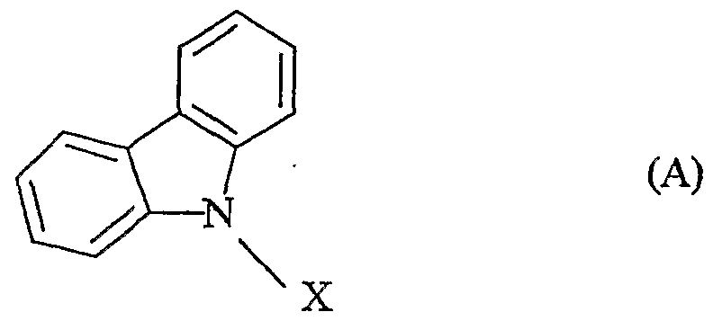
- a 2 represents a substituted or unsubstituted aromatic heterocyclic group containing nitrogen as an atom forming a heterocyclic ring, and is preferably a pyridyl group, a pyrimidyl group, a pyrazine group, a triazine group, a benzothiazole group, or a benzoxazozo.
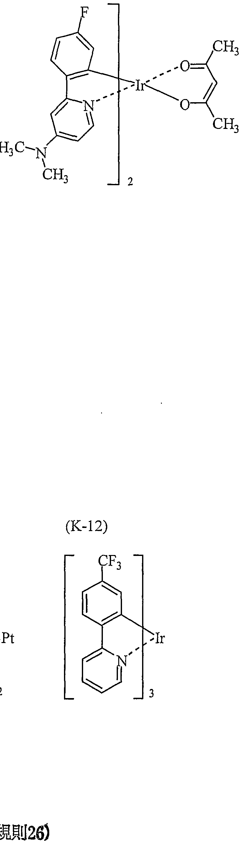
- L represents a bidentate type ligand, and is preferably selected from monodiket type ligands such as acetyl acetonate or pyromellitic acid.
- the hole injecting material has the ability to transport holes, has the effect of injecting holes from the anode, has an excellent hole injecting effect on the light emitting layer or the light emitting material, and has a function of exciters generated in the light emitting layer.
- a compound that prevents migration to an electron injection layer or an electron injection material and has excellent thin film forming ability is preferable.
- more effective hole injection materials are aromatic tertiary amine derivatives or phthalocyanine derivatives.
- aromatic tertiary amine derivatives include triphenylamine, tritriamine, trididiphenylamine,
- phthalocyanine (Pc) derivative H 2 Pc, CuPc, CoPc , N i Pc, ZnPc, PdPc, F ePc, MnPc, C lAl Pc, C l GaP c, C 1 I nP c, C 1 S nP c, C 1 2 S i P c, ( H_ ⁇ ) A l P c, (HO ) GaP c, V0P c, T I_ ⁇ _P c, MoOP c, GaP phthalocyanine derivatives such as c-0-GaPc and naphthalocyanine derivatives, but are not limited thereto.
- fluorenone anthraquinodimethane, diphenoquinone, thiovirane dioxide, oxazole, oxazine diazole, triazole, imidazole, perylene tetracarboxylic acid, quinoxaline, fluorenylidene methane, anthra quinodimethane , Anthrone and the like and derivatives thereof, but are not limited thereto.
- more effective electron injecting materials are metal complex compounds or nitrogen-containing five-membered ring derivatives.
- metal complex compounds include lithium 8-hydroxyquinolinato, bis (8-hydroxyquinolinato) zinc, bis (8-hydroxyquinolinato) copper, and bis (8-hydroxyquinolinato) manganese , Tris (8-hydroxyquinolina) aluminum, tris (2-methyl-18 -hydroxyquinoline) aluminum, tris (8-hydroxyquinoline) aluminum, bis (10-hydroxybenzo [h]) Beryllium, bis (10-hydroxybenzo [h] quinolinato) zinc, bis (2-methyl-18-quinolinato) gallium chloride, bis (2-methyl-18-quinolinato) ( 0—cresolate) Gallium, bis (2-methyl-8-quinolinate) (1-naphtholate) Aluminum, bis (2-meth Lou 8 Kinorina - g) (2-Na full Trad) Gallium like, but is not limited thereto.
- the charge injecting property can be improved by adding an electron accepting substance to the hole injecting material and an electron donating substance to the electron injecting material.
- a material having a work function of more than 4 eV is suitable, and carbon, aluminum, vanadium, iron, cobalt, nickel, tungsten, silver, Gold, platinum, palladium and their alloys, metal oxides such as tin oxide and indium oxide used for ITO and NESA substrates, and organic conductive resins such as polythiophene and polypyrrol .
- the conductive material used for the cathode those having a work function of less than 4 eV are suitable, such as magnesium, calcium, tin, lead, titanium, yttrium, lithium, ruthenium, manganese, aluminum, and the like.
- Typical alloys include magnesium / silver, magnesium / indium, lithium / aluminum, and the like. However, the present invention is not limited to these.
- the ratio of the alloy is controlled by the temperature, atmosphere, degree of vacuum, and the like of the evaporation source, and is selected as an appropriate ratio.
- the anode and the cathode may be formed by two or more layers if necessary.
- the organic EL device of the present invention may have an inorganic compound layer between at least one electrode and the organic thin film layer.
- Preferred inorganic compounds used in the inorganic compound layer include alkali metal oxides, alkaline earth oxides, rare earth oxides, alkali metal halides, alkaline earth halides, rare earth halides, SiOx, A10x, S i N x, S i ON, A10N, Ge_ ⁇ x, L i Ox, L I_ ⁇ _N, T i Ox, T i 0N , TaOx, TaON, TaNx, C and various oxides, nitrides, oxide nitrides is there.
- S i Ox, A 1_Rei x, S i Nx, S i ON, A 1 ON, Ge O x, C is preferable to form a stable injecting interface layer.
- L i F, MgF 2, C aF 2, MgF 2, N a F are preferred.
- At least one surface of the organic EL device of the present invention is sufficiently transparent in the emission wavelength region of the device in order to efficiently emit light. It is also desirable that the substrate is transparent.
- the transparent electrode is set so as to secure a predetermined translucency by a method such as vapor deposition or sputtering using the above conductive material. It is desirable that the electrode on the light emitting surface has a light transmittance of 10% or more.
- the substrate is not limited as long as it has mechanical and thermal strength and is transparent, and examples thereof include a glass substrate and a transparent resin film.
- Transparent resin films include polyethylene, ethylene monobutyl acetate copolymer, ethylene monobutyl alcohol copolymer, polypropylene, polystyrene, polymethyl methacrylate, polyvinyl chloride, polybutyl alcohol, polybutyral, Nylon, polyetheretherketone, polysulfone, polyethersulfone, tetrafluoroethylene-perfluoroalkylvinylether copolymer, polyvinylfluoride, tetrafluoroethylene-ethyl Len copolymer, tetrafluoroethylene-hexafluoropropylene copolymer, polychlorotrifluoroethylene, polyvinylidene fluoride, polyester, polycarbonate, polyurethane, polyimide, polyether Examples include imid, polyimide, and polypropylene.
- a protective layer can be provided on the surface of the device, or the entire device can be protected with silicon oil, resin, or the like, in order to improve stability against temperature, humidity, atmosphere, and the like.
- Each layer of the organic EL device of the present invention is formed by any of dry film forming methods such as vacuum evaporation, sputtering, plasma, and ion plating, and wet film forming methods such as spin coating, dipping, and flow coating. can do.
- the thickness of each layer is not particularly limited, but needs to be set to an appropriate thickness. If the film thickness is too thick, a large applied voltage is required to obtain a constant light output, and the luminous efficiency deteriorates. If the film thickness is too small, pinholes and the like are generated, and sufficient light emission luminance cannot be obtained even when an electric field is applied.
- the normal film thickness is suitably in the range of 5 nm to 10 m, but is more preferably in the range of 10 nm to 0.2 m. '
- the material for forming each layer is dissolved or dispersed in an appropriate solvent such as ethanol, black form, tetrahydrofuran, dioxane or the like to form a thin film.
- an appropriate resin or additive may be used to improve film forming properties, prevent pinholes in the film, and the like.
- Resins that can be used include insulating resins such as polystyrene, polycarbonate, polyarylate, polyester, polyamide, polyurethane, borisulfone, polymethyl methacrylate, polymethyl acrylate, and cell mouth, and the like.
- Examples thereof include photoconductive resins such as polymers, poly-N-vinylcarbazole and polysilane, and conductive resins such as polythiophene and polypyrrole.
- Examples of the additives include an antioxidant, an ultraviolet absorber, and a plasticizer.
- the organic EL device As described above, the general formula (1) or (2) By using the compound of formula (1), an organic EL device having high color purity and emitting blue light can be obtained.
- the organic EL device may be a flat light-emitting device such as an electrophotographic photosensitive member, a flat panel display for a wall-mounted TV, It is suitably used for light sources such as copiers, printers, backlights of liquid crystal displays or instruments, display boards, marker lights, accessories, and the like.
- light sources such as copiers, printers, backlights of liquid crystal displays or instruments, display boards, marker lights, accessories, and the like.
- the triplet energy gap and singlet energy gap of the compound were measured as follows.
- Excitation Singlet energy gap values were measured. That is, the absorbance was measured scan Bae click Bok Le using Hitachi UV-visible absorption analyzer using Toruen soluble liquid samples (1 0 5 mol / liter). A tangent was drawn to the rise on the long wavelength side of the spectrum, and the wavelength (absorption edge) at the intersection with the horizontal axis was determined. This wavelength was converted to an energy value.
- the reaction solution was cooled to room temperature, added with water, extracted with methylene chloride, washed with water, and dried with anhydrous sodium sulfate. After evaporating the organic solvent under reduced pressure, 15 ml of ethyl acetate was added, and the precipitated crystals were filtered and washed with ethyl acetate to obtain 1.9 g of crystals (yield 58%).
- the obtained crystal was confirmed to be the desired product (A9) by 90 MHz 1 H_NMR and FD-MS. FD-MS measurement results are shown below.
- a 25 mm ⁇ 75 mm ⁇ 1.1 mm-thick glass substrate with an IT0 transparent electrode (manufactured by Geoma Tech) was subjected to ultrasonic cleaning in isopropyl alcohol for 5 minutes, and then to UV ozone cleaning for 30 minutes.
- the glass substrate with the transparent electrode line after cleaning is mounted on a substrate holder of a vacuum evaporation apparatus.
- the N, N having a thickness of 6 Onm is formed so as to cover the transparent electrode on the surface on which the transparent electrode line is formed.
- 'N-bis (N, N' diphenyl 4-aminophenyl) 1 N, N-diphenyl 4,4, diamino 1, dibiphenyl film (TPD 232 film) was formed.
- This TFD 232 film functions as a hole injection layer.
- a 4,4'-bis [N- (1-naphthyl) -1N-phenylamino] biphenyl film (NPD film) having a thickness of 2 Onm was formed on the TPD232 film.
- This NPD film functions as a hole transport layer.
- the above compound (A 1) having a thickness of 4 Onm was deposited on the NPD film by vapor deposition.
- the following compound (DI) was vapor-deposited at a weight ratio of (A 1) :( D 1) of 40: 3.
- the compound (D 1) is a light-emitting molecule that emits blue light and has a singlet energy of as low as 2.79 eV.
- the mixed film of the compounds (A1) and (D1) functions as a light emitting layer.
- the following BA1q (Me is a methyl group) was formed on this film at a film thickness of 2 Onm.
- the BA1 q film functions as an electron injection layer.
- a reducing dopant Li Li source: manufactured by SAES Getter Co., Ltd.
- A1q are binary-deposited
- an Alq Li film (film thickness) is formed as a second electron injection layer (cathode). 1 Onm).
- Metal A1 was vapor-deposited on the A1q: Li film to form a metal cathode, thereby manufacturing an organic EL device.
- This device emitted blue light with a high efficiency of 116 cd / m 2 and a luminous efficiency of 4.9 cd / A at a DC voltage of 6. IV.
- the chromaticity coordinates were (0.15, 0.17), indicating high color purity.
- An organic EL device was prepared in the same manner as in Example 1 except that the compound shown in Table 2 was used instead of the compound (A 1). Similarly, a DC voltage, emission luminance, emission efficiency, emission color, and color The purity was measured and is shown in Table 2.
- An organic EL device was prepared in the same manner as in Example 1 except that the compound (A 1) was replaced with the following known compound BCz, which was a conventionally known compound. The efficiency, emission color, and color purity were measured and are shown in Table 2.
- An organic EL device was prepared in the same manner as in Example 1 except that the following compound (C 2) described in JP-A-2001-28884'62 was used instead of the compound (A 1). Make In the same manner, DC voltage, emission luminance, emission efficiency, emission color, and color purity were measured and the results are shown in Table 2.
- the organic EL device using the compound of the present invention is a low-voltage driven and highly efficient blue in comparison with the conventionally known compounds BCz and (C2) of the comparative example. Light emission is obtained.
- the compound of the present invention since the compound of the present invention has a wide energy gap, light-emitting molecules having a wide energy gap can be mixed into the light-emitting layer to emit light.
- a 5 mm x 75 mm x 0.7 mm thick glass substrate with IT ⁇ transparent electrode was subjected to ultrasonic cleaning in isopropyl alcohol for 5 minutes, followed by UV ozone cleaning for 30 minutes. After cleaning, the glass substrate with transparent electrodes is used as the substrate holder for the vacuum evaporation system.
- a 10-nm-thick copper phthalocyanine film (CuPc film described below) was formed on the surface where the transparent electrode was formed so as to cover the transparent electrode. This CuPc film functions as a hole injection layer.
- a 4,4, -bis [N- (1-naphthyl) -N-phenylamino] biphenyl film ( ⁇ -NPD film below) was formed.
- This NPD film functions as a hole transport layer.
- the compound (A1) having a thickness of 30 nm was deposited as a host material on the a-NPD film to form a light emitting layer.
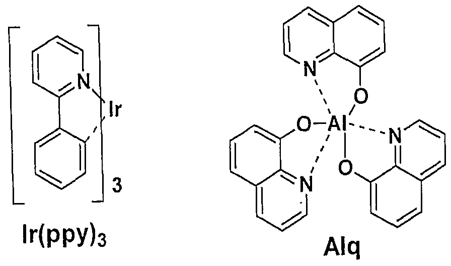
- tris (2-phenylpyridine) Ir (Ir (ppy) 3 below) was added as a phosphorescent Ir metal complex dopant.
- the concentration of Ir (ppy) 3 in the light emitting layer was 5% by weight.
- This film functions as a light emitting layer.
- BA1 q film a film of (1,1-bisphenyl) -141-ortho) bis (2-methyl-8-quinolinolate) aluminum (BA1 q film) having a thickness of 1 Onm was formed.
- BA1 q film functions as a hole barrier layer.
- A1q film a 40 nm-thick aluminum complex of 8-hydroxyquinoline (A1q film described below) was formed on this film.
- This Alq film functions as an electron injection layer.
- LiF which is a halogenated alkali metal, is deposited to a thickness of 0.2 nm, and then aluminum is deposited.
- An organic EL device was prepared in the same manner as in Example 5 except that the compound (A 9) was used instead of the compound (A 1) as the host material of the light emitting layer. Similarly, the voltage, the current density, and the emission luminance The luminous efficiency and chromaticity were measured and are shown in Table 3.
- Example 5 an organic EL device was produced in the same manner as in Example 5, except that the compound (A 1) as the host material of the light-emitting layer was replaced with the compound BCz, which was a conventionally known compound. , Current density, luminous brightness, luminous efficiency, and chromaticity were measured and Comparative Example 4 shown in Table 3
- Example 4 in place of the compound (A 1) of the host material of the light emitting layer, the following compound (A—10) described in US Patent Publication No.
- An organic EL device was manufactured in the same manner except that the above was used, and the DC voltage, current density, light emission luminance, light emission efficiency, and chromaticity were measured in the same manner.
- the organic EL device using the compound of the present invention can emit green light with high efficiency compared to the conventionally known compounds (BCz, A-10) of Comparative Examples 3 and 4. It is possible. Further, since the compound of the present invention has a wide energy gap, light-emitting molecules having a wide energy gap can be mixed into the light-emitting layer to emit light.
- a 25 mm x 75 mm x 0.7 mm thick glass substrate with an IT0 transparent electrode was subjected to ultrasonic cleaning for 5 minutes in isopropyl alcohol, followed by UV ozone cleaning for 30 minutes.
- the washed glass substrate with a transparent electrode is mounted on a substrate holder of a vacuum deposition apparatus.
- a 10-nm-thick copper phthalocyanine film (on the side where the transparent electrode is formed is covered so as to cover the transparent electrode).
- CuP c film was formed.
- This CuP c film functions as a hole injection layer.
- a 3 Nm thick HiPD NPD film was formed on the CuPc film.
- This ⁇ -NPD film functions as a hole transport layer.
- the above compound (A 1) having a thickness of 3 Onm was deposited on the ⁇ -NPD film to form a light emitting layer.
- I r bis I r metal complex phosphorescent was added [(4, 6-difluoro-phenyl) Single Pirijina one DOO one N, C 2 '] Pikorina one Bok (the following FI rp ics). Concentration of FI rp ics in the light emitting layer was 7 wt 0/0. This film functions as a light emitting layer.
- a BA1q film having a thickness of 30 nm was formed. This BA1 q film functions as an electron injection layer.
- LiF which is a metal halide
- LiF which is a metal halide
- aluminum was deposited to a thickness of 150 nm.
- This A 1 / L i F acts as a cathode.
- an organic EL device was manufactured.
- a voltage of 7.2 V, a current density of 0.68 mA / cm 2 , a luminance of 104 cd / m 2 , and a luminous efficiency of 15.4 cd / A were blue. Luminescence was obtained, and the chromaticity coordinates were (0.17, 0.38).
- An organic EL device was prepared in the same manner as in Example 7, except that the compound (A 9) was used instead of the compound (A 1) as the host material of the light emitting layer. Similarly, the voltage, current density, and emission luminance were similarly measured. The luminous efficiency and chromaticity were measured and are shown in Table 4.
- An organic EL device was prepared in the same manner as in Example 7, except that the compound (BC), which was a conventionally known compound, was used in place of the compound (A 1) of the host material for the light emitting layer. Voltage, current density, luminous brightness, luminous efficiency, chromaticity were measured and shown in Table 4.
- the organic EL device using the compound of the present invention is driven at a low voltage and can emit blue light with high luminous efficiency compared to the conventionally known compound BCz of the comparative example.
- the compound of the present invention has a wide energy gap, -Light-emitting molecules having a wide gap can be mixed with the light-emitting layer to emit light.
- the use of the material for an organic electroluminescent device comprising the compound represented by the general formula (1) or (2) of the present invention has high luminous efficiency and color purity, and has a blue color.
- An organic electroluminescent device that emits light can be obtained. Therefore, the organic electroluminescent device of the present invention is extremely useful as a light source for various electronic devices.
Landscapes
- Chemical & Material Sciences (AREA)
- Engineering & Computer Science (AREA)
- Materials Engineering (AREA)
- Organic Chemistry (AREA)
- Physics & Mathematics (AREA)
- Spectroscopy & Molecular Physics (AREA)
- Electroluminescent Light Sources (AREA)
Description


Claims


Priority Applications (4)
| Application Number | Priority Date | Filing Date | Title |
|---|---|---|---|
| JP2003578494A JPWO2003080761A1 (ja) | 2002-03-25 | 2003-03-24 | 有機エレクトロルミネッセンス素子用材料及びそれを用いた有機エレクトロルミネッセンス素子 |
| EP03712849A EP1502936A1 (en) | 2002-03-25 | 2003-03-24 | Material for organic electroluminescent element and organic electroluminescent element employing the same |
| US10/506,196 US20050158578A1 (en) | 2002-03-25 | 2003-03-24 | Material for organic electroluminescent element and organic electroluminescent element employing the same |
| KR10-2004-7015264A KR20040094866A (ko) | 2002-03-25 | 2003-03-24 | 유기 전자발광 소자용 재료 및 이를 이용한 유기 전자발광소자 |
Applications Claiming Priority (2)
| Application Number | Priority Date | Filing Date | Title |
|---|---|---|---|
| JP2002-083866 | 2002-03-25 | ||
| JP2002083866 | 2002-03-25 |
Publications (1)
| Publication Number | Publication Date |
|---|---|
| WO2003080761A1 true WO2003080761A1 (fr) | 2003-10-02 |
Family
ID=28449191
Family Applications (1)
| Application Number | Title | Priority Date | Filing Date |
|---|---|---|---|
| PCT/JP2003/003519 WO2003080761A1 (fr) | 2002-03-25 | 2003-03-24 | Materiau pour element organique electroluminescent et element organique electroluminescent l'utilisant |
Country Status (7)
| Country | Link |
|---|---|
| US (1) | US20050158578A1 (ja) |
| EP (1) | EP1502936A1 (ja) |
| JP (1) | JPWO2003080761A1 (ja) |
| KR (1) | KR20040094866A (ja) |
| CN (1) | CN1656194A (ja) |
| TW (1) | TW200305632A (ja) |
| WO (1) | WO2003080761A1 (ja) |
Cited By (27)
| Publication number | Priority date | Publication date | Assignee | Title |
|---|---|---|---|---|
| JP2004311414A (ja) * | 2003-03-26 | 2004-11-04 | Konica Minolta Holdings Inc | 有機エレクトロルミネッセンス素子、表示装置および照明装置 |
| JP2004311410A (ja) * | 2003-03-26 | 2004-11-04 | Konica Minolta Holdings Inc | 有機エレクトロルミネッセンス素子、照明装置および表示装置 |
| JP2004311412A (ja) * | 2003-03-26 | 2004-11-04 | Konica Minolta Holdings Inc | 有機エレクトロルミネッセンス素子、表示装置及び照明装置 |
| JP2005129478A (ja) * | 2003-09-30 | 2005-05-19 | Konica Minolta Holdings Inc | 有機エレクトロルミネッセンス素子、照明装置、表示装置 |
| JP2005158691A (ja) * | 2003-10-31 | 2005-06-16 | Ricoh Co Ltd | 電界発光素子 |
| JP2005154412A (ja) * | 2003-09-05 | 2005-06-16 | Ricoh Co Ltd | 3,6−ジフェニルカルバゾール誘導体 |
| US7011871B2 (en) | 2004-02-20 | 2006-03-14 | E. I. Du Pont De Nemours And Company | Charge transport compounds and electronic devices made with such compounds |
| JP2006203227A (ja) * | 2006-02-22 | 2006-08-03 | Mitsubishi Chemicals Corp | 有機電界発光素子 |
| JP2007335852A (ja) * | 2006-05-17 | 2007-12-27 | Mitsubishi Chemicals Corp | 電荷輸送材料、有機電界発光素子用組成物、有機電界発光素子用薄膜および有機電界発光素子 |
| JP2008532998A (ja) * | 2005-03-05 | 2008-08-21 | ドゥサン コーポレーション | 新規イリジウム錯体及びこれを用いた有機電界発光素子 |
| CN100427467C (zh) * | 2005-03-03 | 2008-10-22 | 友达光电股份有限公司 | 化合物以及包括该化合物的有机发光二极管与显示器 |
| JP2009035524A (ja) * | 2007-08-03 | 2009-02-19 | Chemiprokasei Kaisha Ltd | 新規なビカルバゾール誘導体、それを用いたホスト材料および有機エレクトロルミネッセンス素子 |
| US7678472B2 (en) | 2005-02-05 | 2010-03-16 | Au Optronics Corp. | Compound and organic light-emitting diode and display utilizing the same |
| JP2010090084A (ja) * | 2008-10-10 | 2010-04-22 | Chemiprokasei Kaisha Ltd | 新規なビス(カルバゾリルフェニル)誘導体、それを用いたホスト材料および有機エレクトロルミネッセンス素子 |
| US7745988B2 (en) * | 2003-09-05 | 2010-06-29 | Ricoh Company, Limited | 3, 6-diphenylcarbazole compound and organic electroluminescent device |
| JP2010161325A (ja) * | 2008-02-28 | 2010-07-22 | Fujifilm Corp | 有機電界発光素子 |
| JP2010161326A (ja) * | 2008-02-28 | 2010-07-22 | Fujifilm Corp | 有機電界発光素子 |
| US7939183B2 (en) * | 2003-12-26 | 2011-05-10 | Idemitsu Kosan Co., Ltd. | Material for organic electroluminescent device and organic electroluminescent device using same |
| US8178215B2 (en) * | 2004-12-10 | 2012-05-15 | Pioneer Corporation | Organic compound containing at least two carbazolyl-substituted phenyl structures; charge-transporting material and organic el element containing the compound |
| WO2012133188A1 (ja) * | 2011-03-25 | 2012-10-04 | 出光興産株式会社 | 有機エレクトロルミネッセンス素子 |
| US8617720B2 (en) | 2009-12-21 | 2013-12-31 | E I Du Pont De Nemours And Company | Electroactive composition and electronic device made with the composition |
| WO2014013947A1 (ja) * | 2012-07-20 | 2014-01-23 | 出光興産株式会社 | 有機エレクトロルミネッセンス素子 |
| US8728633B2 (en) | 2005-06-09 | 2014-05-20 | Konica Minolta Holdings, Inc. | Organic electroluminescent element, illuminator and display |
| WO2014168138A1 (ja) | 2013-04-11 | 2014-10-16 | 新日鉄住金化学株式会社 | 有機電界発光素子用アダマンタン化合物及び有機電界発光素子 |
| US8920942B2 (en) | 2006-03-23 | 2014-12-30 | Konica Minolta Holdings, Inc. | Organic electroluminescent element, display device and illuminating device |
| US8933622B2 (en) | 2005-05-24 | 2015-01-13 | Pioneer Corporation | Organic electroluminescence element |
| US20210066612A1 (en) * | 2019-09-04 | 2021-03-04 | Lg Display Co., Ltd. | Organic compound having improved luminescent properties, organic light emitting diode and organic light emitting device including the organic compound |
Families Citing this family (18)
| Publication number | Priority date | Publication date | Assignee | Title |
|---|---|---|---|---|
| KR100537620B1 (ko) * | 2003-10-29 | 2005-12-19 | 삼성에스디아이 주식회사 | 카바졸 함유 화합물 및 이를 이용한 유기 전계 발광 소자 |
| US20070116982A1 (en) * | 2004-01-21 | 2007-05-24 | Idemitsu Kosan Co., Ltd. | Host material for organic electroluminescent element and organic electroluminescent element |
| JP4351935B2 (ja) * | 2004-03-10 | 2009-10-28 | 富士フイルム株式会社 | 有機電界発光素子 |
| JP2005259523A (ja) * | 2004-03-11 | 2005-09-22 | Idemitsu Kosan Co Ltd | 有機エレクトロルミネッセンス素子、その製造方法及び有機溶液 |
| WO2007108362A1 (ja) * | 2006-03-17 | 2007-09-27 | Konica Minolta Holdings, Inc. | 有機エレクトロルミネッセンス素子、表示装置および照明装置 |
| US7768195B2 (en) * | 2006-05-25 | 2010-08-03 | Idemitsu Kosan Co., Ltd. | Organic electroluminescent device with improved luminous efficiency |
| KR100951707B1 (ko) * | 2007-05-28 | 2010-04-07 | 제일모직주식회사 | 사이클로헥산을 포함하는 유기광전소자용 재료 및 이를포함하는 유기광전소자 |
| JP4531842B2 (ja) * | 2008-04-24 | 2010-08-25 | 富士フイルム株式会社 | 有機電界発光素子 |
| JP5627883B2 (ja) * | 2009-01-07 | 2014-11-19 | ユー・ディー・シー アイルランド リミテッド | 有機電界発光素子 |
| TWI549942B (zh) * | 2010-08-26 | 2016-09-21 | 首威公司 | N-苯基三咔唑類 |
| US9847501B2 (en) | 2011-11-22 | 2017-12-19 | Idemitsu Kosan Co., Ltd. | Aromatic heterocyclic derivative, material for organic electroluminescent element, and organic electroluminescent element |
| US10217954B2 (en) | 2013-11-13 | 2019-02-26 | Idemitsu Kosan Co., Ltd. | Compound, material for organic electroluminescent element, organic electroluminescent element, and electronic device |
| US10784446B2 (en) | 2014-11-28 | 2020-09-22 | Idemitsu Kosan Co., Ltd. | Compound, organic electroluminescence element material, organic electroluminescence element and electronic device |
| KR102660767B1 (ko) * | 2015-02-06 | 2024-04-24 | 이데미쓰 고산 가부시키가이샤 | 유기 일렉트로루미네센스 소자 및 전자 기기 |
| US10862037B2 (en) * | 2015-10-16 | 2020-12-08 | Lg Chem, Ltd. | Electroactive materials |
| KR101880595B1 (ko) * | 2015-12-10 | 2018-07-20 | 성균관대학교산학협력단 | 유기 발광 화합물, 이의 제조 방법 및 이를 포함하는 유기 전계 발광 소자 |
| CN113260608B (zh) * | 2019-11-08 | 2023-12-12 | 株式会社Lg化学 | 新型化合物及包含其的有机发光器件 |
| WO2021091131A1 (ko) * | 2019-11-08 | 2021-05-14 | 주식회사 엘지화학 | 신규한 화합물 및 이를 이용한 유기 발광 소자 |
Citations (11)
| Publication number | Priority date | Publication date | Assignee | Title |
|---|---|---|---|---|
| JPH02129648A (ja) * | 1988-11-10 | 1990-05-17 | Canon Inc | 電子写真感光体 |
| JPH02134643A (ja) * | 1988-11-15 | 1990-05-23 | Canon Inc | 電子写真感光体 |
| JPH06312979A (ja) * | 1993-04-30 | 1994-11-08 | Bando Chem Ind Ltd | 1,3,5−トリス〔4−(n−カルバゾリル)フェニル〕ベンゼン誘導体 |
| US5487953A (en) * | 1993-09-22 | 1996-01-30 | Pioneer Electronic Corporation | Organic electroluminescent device |
| JP2000186066A (ja) * | 1998-12-22 | 2000-07-04 | Minolta Co Ltd | 新規アミノ化合物とその製造方法、及び用途 |
| WO2001041512A1 (en) * | 1999-12-01 | 2001-06-07 | The Trustees Of Princeton University | Complexes of form l2mx as phosphorescent dopants for organic leds |
| WO2001072927A1 (en) * | 2000-03-27 | 2001-10-04 | Idemitsu Kosan Co., Ltd. | Organic electroluminescence device |
| JP2001313179A (ja) * | 2000-05-01 | 2001-11-09 | Mitsubishi Chemicals Corp | 有機電界発光素子 |
| EP1202608A2 (en) * | 2000-10-30 | 2002-05-02 | Kabushiki Kaisha Toyota Chuo Kenkyusho | Organic light-emitting devices |
| JP2002241352A (ja) * | 2001-02-13 | 2002-08-28 | Konica Corp | 新規化合物、それを用いる有機エレクトロルミネッセンス素子材料及び有機エレクトロルミネッセンス素子 |
| JP2003031371A (ja) * | 2001-07-17 | 2003-01-31 | Mitsubishi Chemicals Corp | 有機電界発光素子及び青色発光素子 |
Family Cites Families (13)
| Publication number | Priority date | Publication date | Assignee | Title |
|---|---|---|---|---|
| US5093210A (en) * | 1989-06-30 | 1992-03-03 | Ricoh Company, Ltd. | Electroluminescent device |
| DE4308788A1 (de) * | 1993-03-18 | 1994-09-22 | Bayer Ag | Hetero-tricyclisch-substituierte Phenyl-cyclohexan-carbonsäurederivate |
| EP0681019B1 (en) * | 1994-04-26 | 1999-09-01 | TDK Corporation | Phenylanthracene derivative and organic EL element |
| US6777111B1 (en) * | 1999-08-04 | 2004-08-17 | Kabushiki Kaisha Chuo Kenkyusho | Electro luminescent element |
| JP2001172208A (ja) * | 1999-12-17 | 2001-06-26 | Matsushita Electric Ind Co Ltd | 芳香族メチリデン化合物、それを製造するための芳香族アルデヒド化合物及びそれらの製造方法 |
| JP4562865B2 (ja) * | 2000-06-06 | 2010-10-13 | 三井化学株式会社 | 複素環化合物 |
| JP2002014478A (ja) * | 2000-06-30 | 2002-01-18 | Hodogaya Chem Co Ltd | 電子製品材料の精製方法 |
| US6893743B2 (en) * | 2000-10-04 | 2005-05-17 | Mitsubishi Chemical Corporation | Organic electroluminescent device |
| JP4092901B2 (ja) * | 2000-10-30 | 2008-05-28 | 株式会社豊田中央研究所 | 有機電界発光素子 |
| JP4910238B2 (ja) * | 2001-03-06 | 2012-04-04 | Jsr株式会社 | 化学増幅型感放射線性樹脂組成物 |
| US6863997B2 (en) * | 2001-12-28 | 2005-03-08 | The Trustees Of Princeton University | White light emitting OLEDs from combined monomer and aggregate emission |
| US6562982B1 (en) * | 2002-07-25 | 2003-05-13 | Xerox Corporation | Carbazole compounds |
| KR100537620B1 (ko) * | 2003-10-29 | 2005-12-19 | 삼성에스디아이 주식회사 | 카바졸 함유 화합물 및 이를 이용한 유기 전계 발광 소자 |
-
2003
- 2003-03-24 WO PCT/JP2003/003519 patent/WO2003080761A1/ja active Application Filing
- 2003-03-24 EP EP03712849A patent/EP1502936A1/en not_active Withdrawn
- 2003-03-24 JP JP2003578494A patent/JPWO2003080761A1/ja active Pending
- 2003-03-24 CN CNA038119447A patent/CN1656194A/zh active Pending
- 2003-03-24 US US10/506,196 patent/US20050158578A1/en not_active Abandoned
- 2003-03-24 TW TW092106521A patent/TW200305632A/zh unknown
- 2003-03-24 KR KR10-2004-7015264A patent/KR20040094866A/ko not_active Application Discontinuation
Patent Citations (11)
| Publication number | Priority date | Publication date | Assignee | Title |
|---|---|---|---|---|
| JPH02129648A (ja) * | 1988-11-10 | 1990-05-17 | Canon Inc | 電子写真感光体 |
| JPH02134643A (ja) * | 1988-11-15 | 1990-05-23 | Canon Inc | 電子写真感光体 |
| JPH06312979A (ja) * | 1993-04-30 | 1994-11-08 | Bando Chem Ind Ltd | 1,3,5−トリス〔4−(n−カルバゾリル)フェニル〕ベンゼン誘導体 |
| US5487953A (en) * | 1993-09-22 | 1996-01-30 | Pioneer Electronic Corporation | Organic electroluminescent device |
| JP2000186066A (ja) * | 1998-12-22 | 2000-07-04 | Minolta Co Ltd | 新規アミノ化合物とその製造方法、及び用途 |
| WO2001041512A1 (en) * | 1999-12-01 | 2001-06-07 | The Trustees Of Princeton University | Complexes of form l2mx as phosphorescent dopants for organic leds |
| WO2001072927A1 (en) * | 2000-03-27 | 2001-10-04 | Idemitsu Kosan Co., Ltd. | Organic electroluminescence device |
| JP2001313179A (ja) * | 2000-05-01 | 2001-11-09 | Mitsubishi Chemicals Corp | 有機電界発光素子 |
| EP1202608A2 (en) * | 2000-10-30 | 2002-05-02 | Kabushiki Kaisha Toyota Chuo Kenkyusho | Organic light-emitting devices |
| JP2002241352A (ja) * | 2001-02-13 | 2002-08-28 | Konica Corp | 新規化合物、それを用いる有機エレクトロルミネッセンス素子材料及び有機エレクトロルミネッセンス素子 |
| JP2003031371A (ja) * | 2001-07-17 | 2003-01-31 | Mitsubishi Chemicals Corp | 有機電界発光素子及び青色発光素子 |
Cited By (50)
| Publication number | Priority date | Publication date | Assignee | Title |
|---|---|---|---|---|
| JP2004311410A (ja) * | 2003-03-26 | 2004-11-04 | Konica Minolta Holdings Inc | 有機エレクトロルミネッセンス素子、照明装置および表示装置 |
| JP2004311412A (ja) * | 2003-03-26 | 2004-11-04 | Konica Minolta Holdings Inc | 有機エレクトロルミネッセンス素子、表示装置及び照明装置 |
| JP2004311414A (ja) * | 2003-03-26 | 2004-11-04 | Konica Minolta Holdings Inc | 有機エレクトロルミネッセンス素子、表示装置および照明装置 |
| JP2005154412A (ja) * | 2003-09-05 | 2005-06-16 | Ricoh Co Ltd | 3,6−ジフェニルカルバゾール誘導体 |
| US7745988B2 (en) * | 2003-09-05 | 2010-06-29 | Ricoh Company, Limited | 3, 6-diphenylcarbazole compound and organic electroluminescent device |
| JP2005129478A (ja) * | 2003-09-30 | 2005-05-19 | Konica Minolta Holdings Inc | 有機エレクトロルミネッセンス素子、照明装置、表示装置 |
| JP2005158691A (ja) * | 2003-10-31 | 2005-06-16 | Ricoh Co Ltd | 電界発光素子 |
| US7939183B2 (en) * | 2003-12-26 | 2011-05-10 | Idemitsu Kosan Co., Ltd. | Material for organic electroluminescent device and organic electroluminescent device using same |
| US7011871B2 (en) | 2004-02-20 | 2006-03-14 | E. I. Du Pont De Nemours And Company | Charge transport compounds and electronic devices made with such compounds |
| US8178215B2 (en) * | 2004-12-10 | 2012-05-15 | Pioneer Corporation | Organic compound containing at least two carbazolyl-substituted phenyl structures; charge-transporting material and organic el element containing the compound |
| US7678472B2 (en) | 2005-02-05 | 2010-03-16 | Au Optronics Corp. | Compound and organic light-emitting diode and display utilizing the same |
| CN100427467C (zh) * | 2005-03-03 | 2008-10-22 | 友达光电股份有限公司 | 化合物以及包括该化合物的有机发光二极管与显示器 |
| JP2008532998A (ja) * | 2005-03-05 | 2008-08-21 | ドゥサン コーポレーション | 新規イリジウム錯体及びこれを用いた有機電界発光素子 |
| US8933622B2 (en) | 2005-05-24 | 2015-01-13 | Pioneer Corporation | Organic electroluminescence element |
| US8728633B2 (en) | 2005-06-09 | 2014-05-20 | Konica Minolta Holdings, Inc. | Organic electroluminescent element, illuminator and display |
| US9428687B2 (en) | 2005-06-09 | 2016-08-30 | Konica Minolta Holdings, Inc. | Organic electroluminescent element, illuminator and display |
| US8808874B2 (en) * | 2005-06-09 | 2014-08-19 | Konica Minolta Holdings, Inc. | Organic electroluminescent element, illuminator and display |
| JP2006203227A (ja) * | 2006-02-22 | 2006-08-03 | Mitsubishi Chemicals Corp | 有機電界発光素子 |
| JP4677926B2 (ja) * | 2006-02-22 | 2011-04-27 | 三菱化学株式会社 | 有機電界発光素子 |
| US9692000B2 (en) | 2006-03-23 | 2017-06-27 | Konica Minolta, Inc. | Organic electroluminescent element, display device and illuminating device |
| US9634275B2 (en) | 2006-03-23 | 2017-04-25 | Konica Minolta, Inc. | Organic electroluminescent element, display device and illuminating device |
| US9634276B2 (en) | 2006-03-23 | 2017-04-25 | Konica Minolta, Inc. | Organic electroluminescent element, display device and illuminating device |
| US8920942B2 (en) | 2006-03-23 | 2014-12-30 | Konica Minolta Holdings, Inc. | Organic electroluminescent element, display device and illuminating device |
| JP2007335852A (ja) * | 2006-05-17 | 2007-12-27 | Mitsubishi Chemicals Corp | 電荷輸送材料、有機電界発光素子用組成物、有機電界発光素子用薄膜および有機電界発光素子 |
| JP2009035524A (ja) * | 2007-08-03 | 2009-02-19 | Chemiprokasei Kaisha Ltd | 新規なビカルバゾール誘導体、それを用いたホスト材料および有機エレクトロルミネッセンス素子 |
| JP2010161326A (ja) * | 2008-02-28 | 2010-07-22 | Fujifilm Corp | 有機電界発光素子 |
| JP2010161325A (ja) * | 2008-02-28 | 2010-07-22 | Fujifilm Corp | 有機電界発光素子 |
| JP2010090084A (ja) * | 2008-10-10 | 2010-04-22 | Chemiprokasei Kaisha Ltd | 新規なビス(カルバゾリルフェニル)誘導体、それを用いたホスト材料および有機エレクトロルミネッセンス素子 |
| US8617720B2 (en) | 2009-12-21 | 2013-12-31 | E I Du Pont De Nemours And Company | Electroactive composition and electronic device made with the composition |
| KR20140015385A (ko) * | 2011-03-25 | 2014-02-06 | 이데미쓰 고산 가부시키가이샤 | 유기 일렉트로 루미네선스 소자 |
| KR102018418B1 (ko) | 2011-03-25 | 2019-09-04 | 이데미쓰 고산 가부시키가이샤 | 유기 일렉트로 루미네선스 소자 |
| JPWO2012133188A1 (ja) * | 2011-03-25 | 2014-07-28 | 出光興産株式会社 | 有機エレクトロルミネッセンス素子 |
| US10879482B2 (en) | 2011-03-25 | 2020-12-29 | Idemitsu Kosan Co., Ltd. | Organic electroluminescence device |
| WO2012133188A1 (ja) * | 2011-03-25 | 2012-10-04 | 出光興産株式会社 | 有機エレクトロルミネッセンス素子 |
| US8643268B2 (en) | 2011-03-25 | 2014-02-04 | Idemitsu Kosan Co., Ltd. | Organic electroluminescence device |
| JP5889280B2 (ja) * | 2011-03-25 | 2016-03-22 | 出光興産株式会社 | 有機エレクトロルミネッセンス素子 |
| KR101650996B1 (ko) | 2011-03-25 | 2016-08-24 | 이데미쓰 고산 가부시키가이샤 | 유기 일렉트로 루미네선스 소자 |
| KR20160101214A (ko) * | 2011-03-25 | 2016-08-24 | 이데미쓰 고산 가부시키가이샤 | 유기 일렉트로 루미네선스 소자 |
| US9608209B2 (en) | 2012-07-20 | 2017-03-28 | Idemitsu Kosan Co., Ltd. | Organic electroluminescent element |
| JP2014022666A (ja) * | 2012-07-20 | 2014-02-03 | Idemitsu Kosan Co Ltd | 有機エレクトロルミネッセンス素子 |
| WO2014013947A1 (ja) * | 2012-07-20 | 2014-01-23 | 出光興産株式会社 | 有機エレクトロルミネッセンス素子 |
| US9219242B2 (en) | 2012-07-20 | 2015-12-22 | Idemitsu Kosan Co., Ltd. | Organic electroluminescent element |
| US10032998B2 (en) | 2012-07-20 | 2018-07-24 | Idemitsu Kosan Co., Ltd. | Organic electroluminescent element |
| US10461264B2 (en) | 2012-07-20 | 2019-10-29 | Idemitsu Kosan Co., Ltd. | Organic electroluminescent element |
| US10930860B2 (en) | 2012-07-20 | 2021-02-23 | Idemitsu Kosan Co., Ltd. | Organic electroluminescent element |
| CN105190930A (zh) * | 2013-04-11 | 2015-12-23 | 新日铁住金化学株式会社 | 有机电致发光元件用金刚烷化合物及有机电致发光元件 |
| US9722189B2 (en) | 2013-04-11 | 2017-08-01 | Nippon Steel & Sumikin Chemical Co., Ltd. | Adamantane compound for organic electroluminescent elements, and organic electroluminescent element |
| WO2014168138A1 (ja) | 2013-04-11 | 2014-10-16 | 新日鉄住金化学株式会社 | 有機電界発光素子用アダマンタン化合物及び有機電界発光素子 |
| KR20150139969A (ko) | 2013-04-11 | 2015-12-14 | 신닛테츠 수미킨 가가쿠 가부시키가이샤 | 유기 전계 발광 소자용 아다만탄 화합물 및 유기 전계 발광 소자 |
| US20210066612A1 (en) * | 2019-09-04 | 2021-03-04 | Lg Display Co., Ltd. | Organic compound having improved luminescent properties, organic light emitting diode and organic light emitting device including the organic compound |
Also Published As
| Publication number | Publication date |
|---|---|
| KR20040094866A (ko) | 2004-11-10 |
| JPWO2003080761A1 (ja) | 2005-07-21 |
| TW200305632A (en) | 2003-11-01 |
| EP1502936A1 (en) | 2005-02-02 |
| US20050158578A1 (en) | 2005-07-21 |
| CN1656194A (zh) | 2005-08-17 |
Similar Documents
| Publication | Publication Date | Title |
|---|---|---|
| WO2003080761A1 (fr) | Materiau pour element organique electroluminescent et element organique electroluminescent l'utilisant | |
| JP4060802B2 (ja) | 有機エレクトロルミネッセンス素子用材料及びそれを用いた有機エレクトロルミネッセンス素子 | |
| KR100948700B1 (ko) | 유기 전기 발광 소자용 재료 및 이를 이용한 유기 전기발광 소자 | |
| JP3498533B2 (ja) | 有機エレクトロルミネッセンス素子用発光材料およびそれを使用した有機エレクトロルミネッセンス素子 | |
| JP4002040B2 (ja) | 有機エレクトロルミネッセンス素子 | |
| WO2004044088A1 (ja) | 有機エレクトロルミネッセンス素子用材料及びそれを用いた有機エレクトロルミネッセンス素子 | |
| WO2004101491A1 (ja) | アリールアミン化合物及びそれを用いた有機エレクトロルミネッセンス素子 | |
| WO2004092111A1 (ja) | 芳香族アミン誘導体及びそれを用いた有機エレクトロルミネッセンス素子 | |
| KR20020062940A (ko) | 신규 아릴아민 화합물 및 유기 전기발광 소자 | |
| JP2003201472A (ja) | 有機エレクトロルミネッセンス素子用材料およびそれを使用した有機エレクトロルミネッセンス素子 | |
| WO2002020459A1 (fr) | Nouveaux composes de styryle et dispositifs electroluminescents organiques | |
| JP2003129043A (ja) | 有機エレクトロルミネッセンス素子用材料およびそれを使用した有機エレクトロルミネッセンス素子 | |
| JP2008147424A (ja) | 有機エレクトロルミネッセンス素子 | |
| JP3475620B2 (ja) | 有機エレクトロルミネッセンス素子材料およびそれを使用した有機エレクトロルミネッセンス素子 | |
| JP2000290645A (ja) | 有機エレクトロルミネッセンス素子用材料およびそれを使用した有機エレクトロルミネッセンス素子 | |
| JP2008147400A (ja) | 有機エレクトロルミネッセンス素子 | |
| JP2005113072A (ja) | 有機エレクトロルミネッセンス素子用材料およびそれを用いた有機エレクトロルミネッセンス素子 | |
| JP2003313547A (ja) | 有機エレクトロルミネッセンス素子用材料及びそれを用いた有機エレクトロルミネッセンス素子 | |
| JP3985895B2 (ja) | 有機エレクトロルミネッセンス素子用材料及びそれを用いた有機エレクトロルミネッセンス素子 | |
| JP2000268975A (ja) | 有機エレクトロルミネッセンス素子 | |
| JP4028996B2 (ja) | 有機エレクトロルミネッセンス素子用材料及びそれを用いた有機エレクトロルミネッセンス素子 | |
| JPH11317290A (ja) | 有機電界発光素子 | |
| JP2003068462A (ja) | 有機エレクトロルミネッセンス素子用材料およびそれを使用した有機エレクトロルミネッセンス素子 | |
| JP2003020477A (ja) | 有機エレクトロルミネッセンス素子用材料およびそれを使用した有機エレクトロルミネッセンス素子 | |
| JP2002329579A (ja) | 発光素子 |
Legal Events
| Date | Code | Title | Description |
|---|---|---|---|
| AK | Designated states |
Kind code of ref document: A1 Designated state(s): CN IN JP KR US |
|
| AL | Designated countries for regional patents |
Kind code of ref document: A1 Designated state(s): AT BE BG CH CY CZ DE DK EE ES FI FR GB GR HU IE IT LU MC NL PT RO SE SI SK TR |
|
| 121 | Ep: the epo has been informed by wipo that ep was designated in this application | ||
| WWE | Wipo information: entry into national phase |
Ref document number: 2003578494 Country of ref document: JP |
|
| WWE | Wipo information: entry into national phase |
Ref document number: 2003712849 Country of ref document: EP |
|
| WWE | Wipo information: entry into national phase |
Ref document number: 2091/CHENP/2004 Country of ref document: IN |
|
| WWE | Wipo information: entry into national phase |
Ref document number: 1020047015264 Country of ref document: KR |
|
| WWE | Wipo information: entry into national phase |
Ref document number: 10506196 Country of ref document: US |
|
| WWP | Wipo information: published in national office |
Ref document number: 1020047015264 Country of ref document: KR |
|
| WWE | Wipo information: entry into national phase |
Ref document number: 20038119447 Country of ref document: CN |
|
| WWP | Wipo information: published in national office |
Ref document number: 2003712849 Country of ref document: EP |