US9536998B2 - Semiconductor device and semiconductor device manufacturing method - Google Patents
Semiconductor device and semiconductor device manufacturing method Download PDFInfo
- Publication number
- US9536998B2 US9536998B2 US14/397,073 US201314397073A US9536998B2 US 9536998 B2 US9536998 B2 US 9536998B2 US 201314397073 A US201314397073 A US 201314397073A US 9536998 B2 US9536998 B2 US 9536998B2
- Authority
- US
- United States
- Prior art keywords
- gate
- layer
- insulating film
- semiconductor device
- trench
- Prior art date
- Legal status (The legal status is an assumption and is not a legal conclusion. Google has not performed a legal analysis and makes no representation as to the accuracy of the status listed.)
- Active
Links
- 239000004065 semiconductor Substances 0.000 title claims abstract description 108
- 238000004519 manufacturing process Methods 0.000 title abstract description 14
- 239000010410 layer Substances 0.000 claims description 166
- 239000011229 interlayer Substances 0.000 claims description 12
- 229910021420 polycrystalline silicon Inorganic materials 0.000 claims description 10
- 229920005591 polysilicon Polymers 0.000 claims description 10
- 229910052782 aluminium Inorganic materials 0.000 claims description 5
- XAGFODPZIPBFFR-UHFFFAOYSA-N aluminium Chemical compound [Al] XAGFODPZIPBFFR-UHFFFAOYSA-N 0.000 claims description 5
- 239000000758 substrate Substances 0.000 abstract description 45
- 238000000034 method Methods 0.000 abstract description 7
- HBMJWWWQQXIZIP-UHFFFAOYSA-N silicon carbide Chemical compound [Si+]#[C-] HBMJWWWQQXIZIP-UHFFFAOYSA-N 0.000 description 46
- 229910010271 silicon carbide Inorganic materials 0.000 description 46
- 230000005684 electric field Effects 0.000 description 22
- 108091006146 Channels Proteins 0.000 description 17
- 108010075750 P-Type Calcium Channels Proteins 0.000 description 16
- 230000015572 biosynthetic process Effects 0.000 description 8
- 230000015556 catabolic process Effects 0.000 description 8
- 238000005520 cutting process Methods 0.000 description 6
- 239000003990 capacitor Substances 0.000 description 4
- 238000005229 chemical vapour deposition Methods 0.000 description 4
- 230000000694 effects Effects 0.000 description 4
- 239000007789 gas Substances 0.000 description 4
- 238000000137 annealing Methods 0.000 description 3
- 230000005669 field effect Effects 0.000 description 3
- 239000012535 impurity Substances 0.000 description 3
- 238000007254 oxidation reaction Methods 0.000 description 3
- 238000010586 diagram Methods 0.000 description 2
- 239000011810 insulating material Substances 0.000 description 2
- UFHFLCQGNIYNRP-UHFFFAOYSA-N Hydrogen Chemical compound [H][H] UFHFLCQGNIYNRP-UHFFFAOYSA-N 0.000 description 1
- VYPSYNLAJGMNEJ-UHFFFAOYSA-N Silicium dioxide Chemical compound O=[Si]=O VYPSYNLAJGMNEJ-UHFFFAOYSA-N 0.000 description 1
- 239000012141 concentrate Substances 0.000 description 1
- 238000000151 deposition Methods 0.000 description 1
- 229910003460 diamond Inorganic materials 0.000 description 1
- 239000010432 diamond Substances 0.000 description 1
- 238000005530 etching Methods 0.000 description 1
- 238000001704 evaporation Methods 0.000 description 1
- 230000001747 exhibiting effect Effects 0.000 description 1
- 230000012447 hatching Effects 0.000 description 1
- 239000001257 hydrogen Substances 0.000 description 1
- 229910052739 hydrogen Inorganic materials 0.000 description 1
- 239000011159 matrix material Substances 0.000 description 1
- 239000007769 metal material Substances 0.000 description 1
- 230000003647 oxidation Effects 0.000 description 1
- 230000002265 prevention Effects 0.000 description 1
- 229910052814 silicon oxide Inorganic materials 0.000 description 1
- 238000004544 sputter deposition Methods 0.000 description 1
Images


Classifications
-
- H—ELECTRICITY
- H01—ELECTRIC ELEMENTS
- H01L—SEMICONDUCTOR DEVICES NOT COVERED BY CLASS H10
- H01L21/00—Processes or apparatus adapted for the manufacture or treatment of semiconductor or solid state devices or of parts thereof
- H01L21/02—Manufacture or treatment of semiconductor devices or of parts thereof
- H01L21/02104—Forming layers
- H01L21/02107—Forming insulating materials on a substrate
- H01L21/02225—Forming insulating materials on a substrate characterised by the process for the formation of the insulating layer
- H01L21/02227—Forming insulating materials on a substrate characterised by the process for the formation of the insulating layer formation by a process other than a deposition process
- H01L21/0223—Forming insulating materials on a substrate characterised by the process for the formation of the insulating layer formation by a process other than a deposition process formation by oxidation, e.g. oxidation of the substrate
- H01L21/02233—Forming insulating materials on a substrate characterised by the process for the formation of the insulating layer formation by a process other than a deposition process formation by oxidation, e.g. oxidation of the substrate of the semiconductor substrate or a semiconductor layer
-
- H—ELECTRICITY
- H01—ELECTRIC ELEMENTS
- H01L—SEMICONDUCTOR DEVICES NOT COVERED BY CLASS H10
- H01L21/00—Processes or apparatus adapted for the manufacture or treatment of semiconductor or solid state devices or of parts thereof
- H01L21/02—Manufacture or treatment of semiconductor devices or of parts thereof
- H01L21/04—Manufacture or treatment of semiconductor devices or of parts thereof the devices having potential barriers, e.g. a PN junction, depletion layer or carrier concentration layer
- H01L21/0445—Manufacture or treatment of semiconductor devices or of parts thereof the devices having potential barriers, e.g. a PN junction, depletion layer or carrier concentration layer the devices having semiconductor bodies comprising crystalline silicon carbide
- H01L21/048—Making electrodes
- H01L21/049—Conductor-insulator-semiconductor electrodes, e.g. MIS contacts
-
- H—ELECTRICITY
- H01—ELECTRIC ELEMENTS
- H01L—SEMICONDUCTOR DEVICES NOT COVERED BY CLASS H10
- H01L29/00—Semiconductor devices specially adapted for rectifying, amplifying, oscillating or switching and having potential barriers; Capacitors or resistors having potential barriers, e.g. a PN-junction depletion layer or carrier concentration layer; Details of semiconductor bodies or of electrodes thereof ; Multistep manufacturing processes therefor
- H01L29/02—Semiconductor bodies ; Multistep manufacturing processes therefor
- H01L29/06—Semiconductor bodies ; Multistep manufacturing processes therefor characterised by their shape; characterised by the shapes, relative sizes, or dispositions of the semiconductor regions ; characterised by the concentration or distribution of impurities within semiconductor regions
- H01L29/10—Semiconductor bodies ; Multistep manufacturing processes therefor characterised by their shape; characterised by the shapes, relative sizes, or dispositions of the semiconductor regions ; characterised by the concentration or distribution of impurities within semiconductor regions with semiconductor regions connected to an electrode not carrying current to be rectified, amplified or switched and such electrode being part of a semiconductor device which comprises three or more electrodes
- H01L29/1095—Body region, i.e. base region, of DMOS transistors or IGBTs
-
- H—ELECTRICITY
- H01—ELECTRIC ELEMENTS
- H01L—SEMICONDUCTOR DEVICES NOT COVERED BY CLASS H10
- H01L29/00—Semiconductor devices specially adapted for rectifying, amplifying, oscillating or switching and having potential barriers; Capacitors or resistors having potential barriers, e.g. a PN-junction depletion layer or carrier concentration layer; Details of semiconductor bodies or of electrodes thereof ; Multistep manufacturing processes therefor
- H01L29/40—Electrodes ; Multistep manufacturing processes therefor
- H01L29/401—Multistep manufacturing processes
-
- H—ELECTRICITY
- H01—ELECTRIC ELEMENTS
- H01L—SEMICONDUCTOR DEVICES NOT COVERED BY CLASS H10
- H01L29/00—Semiconductor devices specially adapted for rectifying, amplifying, oscillating or switching and having potential barriers; Capacitors or resistors having potential barriers, e.g. a PN-junction depletion layer or carrier concentration layer; Details of semiconductor bodies or of electrodes thereof ; Multistep manufacturing processes therefor
- H01L29/40—Electrodes ; Multistep manufacturing processes therefor
- H01L29/41—Electrodes ; Multistep manufacturing processes therefor characterised by their shape, relative sizes or dispositions
- H01L29/423—Electrodes ; Multistep manufacturing processes therefor characterised by their shape, relative sizes or dispositions not carrying the current to be rectified, amplified or switched
- H01L29/42312—Gate electrodes for field effect devices
- H01L29/42316—Gate electrodes for field effect devices for field-effect transistors
- H01L29/4232—Gate electrodes for field effect devices for field-effect transistors with insulated gate
- H01L29/42364—Gate electrodes for field effect devices for field-effect transistors with insulated gate characterised by the insulating layer, e.g. thickness or uniformity
- H01L29/42368—Gate electrodes for field effect devices for field-effect transistors with insulated gate characterised by the insulating layer, e.g. thickness or uniformity the thickness being non-uniform
-
- H—ELECTRICITY
- H01—ELECTRIC ELEMENTS
- H01L—SEMICONDUCTOR DEVICES NOT COVERED BY CLASS H10
- H01L29/00—Semiconductor devices specially adapted for rectifying, amplifying, oscillating or switching and having potential barriers; Capacitors or resistors having potential barriers, e.g. a PN-junction depletion layer or carrier concentration layer; Details of semiconductor bodies or of electrodes thereof ; Multistep manufacturing processes therefor
- H01L29/66—Types of semiconductor device ; Multistep manufacturing processes therefor
- H01L29/66007—Multistep manufacturing processes
- H01L29/66053—Multistep manufacturing processes of devices having a semiconductor body comprising crystalline silicon carbide
- H01L29/66068—Multistep manufacturing processes of devices having a semiconductor body comprising crystalline silicon carbide the devices being controllable only by the electric current supplied or the electric potential applied, to an electrode which does not carry the current to be rectified, amplified or switched, e.g. three-terminal devices
-
- H—ELECTRICITY
- H01—ELECTRIC ELEMENTS
- H01L—SEMICONDUCTOR DEVICES NOT COVERED BY CLASS H10
- H01L29/00—Semiconductor devices specially adapted for rectifying, amplifying, oscillating or switching and having potential barriers; Capacitors or resistors having potential barriers, e.g. a PN-junction depletion layer or carrier concentration layer; Details of semiconductor bodies or of electrodes thereof ; Multistep manufacturing processes therefor
- H01L29/66—Types of semiconductor device ; Multistep manufacturing processes therefor
- H01L29/66007—Multistep manufacturing processes
- H01L29/66075—Multistep manufacturing processes of devices having semiconductor bodies comprising group 14 or group 13/15 materials
- H01L29/66227—Multistep manufacturing processes of devices having semiconductor bodies comprising group 14 or group 13/15 materials the devices being controllable only by the electric current supplied or the electric potential applied, to an electrode which does not carry the current to be rectified, amplified or switched, e.g. three-terminal devices
- H01L29/66409—Unipolar field-effect transistors
- H01L29/66477—Unipolar field-effect transistors with an insulated gate, i.e. MISFET
- H01L29/66674—DMOS transistors, i.e. MISFETs with a channel accommodating body or base region adjoining a drain drift region
- H01L29/66712—Vertical DMOS transistors, i.e. VDMOS transistors
- H01L29/66734—Vertical DMOS transistors, i.e. VDMOS transistors with a step of recessing the gate electrode, e.g. to form a trench gate electrode
-
- H—ELECTRICITY
- H01—ELECTRIC ELEMENTS
- H01L—SEMICONDUCTOR DEVICES NOT COVERED BY CLASS H10
- H01L29/00—Semiconductor devices specially adapted for rectifying, amplifying, oscillating or switching and having potential barriers; Capacitors or resistors having potential barriers, e.g. a PN-junction depletion layer or carrier concentration layer; Details of semiconductor bodies or of electrodes thereof ; Multistep manufacturing processes therefor
- H01L29/66—Types of semiconductor device ; Multistep manufacturing processes therefor
- H01L29/68—Types of semiconductor device ; Multistep manufacturing processes therefor controllable by only the electric current supplied, or only the electric potential applied, to an electrode which does not carry the current to be rectified, amplified or switched
- H01L29/76—Unipolar devices, e.g. field effect transistors
- H01L29/772—Field effect transistors
- H01L29/78—Field effect transistors with field effect produced by an insulated gate
- H01L29/7801—DMOS transistors, i.e. MISFETs with a channel accommodating body or base region adjoining a drain drift region
- H01L29/7802—Vertical DMOS transistors, i.e. VDMOS transistors
- H01L29/7811—Vertical DMOS transistors, i.e. VDMOS transistors with an edge termination structure
-
- H—ELECTRICITY
- H01—ELECTRIC ELEMENTS
- H01L—SEMICONDUCTOR DEVICES NOT COVERED BY CLASS H10
- H01L29/00—Semiconductor devices specially adapted for rectifying, amplifying, oscillating or switching and having potential barriers; Capacitors or resistors having potential barriers, e.g. a PN-junction depletion layer or carrier concentration layer; Details of semiconductor bodies or of electrodes thereof ; Multistep manufacturing processes therefor
- H01L29/66—Types of semiconductor device ; Multistep manufacturing processes therefor
- H01L29/68—Types of semiconductor device ; Multistep manufacturing processes therefor controllable by only the electric current supplied, or only the electric potential applied, to an electrode which does not carry the current to be rectified, amplified or switched
- H01L29/76—Unipolar devices, e.g. field effect transistors
- H01L29/772—Field effect transistors
- H01L29/78—Field effect transistors with field effect produced by an insulated gate
- H01L29/7801—DMOS transistors, i.e. MISFETs with a channel accommodating body or base region adjoining a drain drift region
- H01L29/7802—Vertical DMOS transistors, i.e. VDMOS transistors
- H01L29/7813—Vertical DMOS transistors, i.e. VDMOS transistors with trench gate electrode, e.g. UMOS transistors
-
- H—ELECTRICITY
- H01—ELECTRIC ELEMENTS
- H01L—SEMICONDUCTOR DEVICES NOT COVERED BY CLASS H10
- H01L21/00—Processes or apparatus adapted for the manufacture or treatment of semiconductor or solid state devices or of parts thereof
- H01L21/02—Manufacture or treatment of semiconductor devices or of parts thereof
- H01L21/02104—Forming layers
- H01L21/02107—Forming insulating materials on a substrate
- H01L21/02225—Forming insulating materials on a substrate characterised by the process for the formation of the insulating layer
- H01L21/02227—Forming insulating materials on a substrate characterised by the process for the formation of the insulating layer formation by a process other than a deposition process
- H01L21/02255—Forming insulating materials on a substrate characterised by the process for the formation of the insulating layer formation by a process other than a deposition process formation by thermal treatment
-
- H—ELECTRICITY
- H01—ELECTRIC ELEMENTS
- H01L—SEMICONDUCTOR DEVICES NOT COVERED BY CLASS H10
- H01L21/00—Processes or apparatus adapted for the manufacture or treatment of semiconductor or solid state devices or of parts thereof
- H01L21/02—Manufacture or treatment of semiconductor devices or of parts thereof
- H01L21/04—Manufacture or treatment of semiconductor devices or of parts thereof the devices having potential barriers, e.g. a PN junction, depletion layer or carrier concentration layer
- H01L21/18—Manufacture or treatment of semiconductor devices or of parts thereof the devices having potential barriers, e.g. a PN junction, depletion layer or carrier concentration layer the devices having semiconductor bodies comprising elements of Group IV of the Periodic Table or AIIIBV compounds with or without impurities, e.g. doping materials
- H01L21/30—Treatment of semiconductor bodies using processes or apparatus not provided for in groups H01L21/20 - H01L21/26
- H01L21/324—Thermal treatment for modifying the properties of semiconductor bodies, e.g. annealing, sintering
- H01L21/3247—Thermal treatment for modifying the properties of semiconductor bodies, e.g. annealing, sintering for altering the shape, e.g. smoothing the surface
-
- H—ELECTRICITY
- H01—ELECTRIC ELEMENTS
- H01L—SEMICONDUCTOR DEVICES NOT COVERED BY CLASS H10
- H01L2224/00—Indexing scheme for arrangements for connecting or disconnecting semiconductor or solid-state bodies and methods related thereto as covered by H01L24/00
- H01L2224/01—Means for bonding being attached to, or being formed on, the surface to be connected, e.g. chip-to-package, die-attach, "first-level" interconnects; Manufacturing methods related thereto
- H01L2224/02—Bonding areas; Manufacturing methods related thereto
- H01L2224/04—Structure, shape, material or disposition of the bonding areas prior to the connecting process
- H01L2224/06—Structure, shape, material or disposition of the bonding areas prior to the connecting process of a plurality of bonding areas
- H01L2224/0601—Structure
- H01L2224/0603—Bonding areas having different sizes, e.g. different heights or widths
-
- H—ELECTRICITY
- H01—ELECTRIC ELEMENTS
- H01L—SEMICONDUCTOR DEVICES NOT COVERED BY CLASS H10
- H01L29/00—Semiconductor devices specially adapted for rectifying, amplifying, oscillating or switching and having potential barriers; Capacitors or resistors having potential barriers, e.g. a PN-junction depletion layer or carrier concentration layer; Details of semiconductor bodies or of electrodes thereof ; Multistep manufacturing processes therefor
- H01L29/02—Semiconductor bodies ; Multistep manufacturing processes therefor
- H01L29/06—Semiconductor bodies ; Multistep manufacturing processes therefor characterised by their shape; characterised by the shapes, relative sizes, or dispositions of the semiconductor regions ; characterised by the concentration or distribution of impurities within semiconductor regions
- H01L29/0603—Semiconductor bodies ; Multistep manufacturing processes therefor characterised by their shape; characterised by the shapes, relative sizes, or dispositions of the semiconductor regions ; characterised by the concentration or distribution of impurities within semiconductor regions characterised by particular constructional design considerations, e.g. for preventing surface leakage, for controlling electric field concentration or for internal isolations regions
- H01L29/0607—Semiconductor bodies ; Multistep manufacturing processes therefor characterised by their shape; characterised by the shapes, relative sizes, or dispositions of the semiconductor regions ; characterised by the concentration or distribution of impurities within semiconductor regions characterised by particular constructional design considerations, e.g. for preventing surface leakage, for controlling electric field concentration or for internal isolations regions for preventing surface leakage or controlling electric field concentration
- H01L29/0611—Semiconductor bodies ; Multistep manufacturing processes therefor characterised by their shape; characterised by the shapes, relative sizes, or dispositions of the semiconductor regions ; characterised by the concentration or distribution of impurities within semiconductor regions characterised by particular constructional design considerations, e.g. for preventing surface leakage, for controlling electric field concentration or for internal isolations regions for preventing surface leakage or controlling electric field concentration for increasing or controlling the breakdown voltage of reverse biased devices
- H01L29/0615—Semiconductor bodies ; Multistep manufacturing processes therefor characterised by their shape; characterised by the shapes, relative sizes, or dispositions of the semiconductor regions ; characterised by the concentration or distribution of impurities within semiconductor regions characterised by particular constructional design considerations, e.g. for preventing surface leakage, for controlling electric field concentration or for internal isolations regions for preventing surface leakage or controlling electric field concentration for increasing or controlling the breakdown voltage of reverse biased devices by the doping profile or the shape or the arrangement of the PN junction, or with supplementary regions, e.g. junction termination extension [JTE]
- H01L29/063—Reduced surface field [RESURF] pn-junction structures
- H01L29/0634—Multiple reduced surface field (multi-RESURF) structures, e.g. double RESURF, charge compensation, cool, superjunction (SJ), 3D-RESURF, composite buffer (CB) structures
-
- H—ELECTRICITY
- H01—ELECTRIC ELEMENTS
- H01L—SEMICONDUCTOR DEVICES NOT COVERED BY CLASS H10
- H01L29/00—Semiconductor devices specially adapted for rectifying, amplifying, oscillating or switching and having potential barriers; Capacitors or resistors having potential barriers, e.g. a PN-junction depletion layer or carrier concentration layer; Details of semiconductor bodies or of electrodes thereof ; Multistep manufacturing processes therefor
- H01L29/02—Semiconductor bodies ; Multistep manufacturing processes therefor
- H01L29/12—Semiconductor bodies ; Multistep manufacturing processes therefor characterised by the materials of which they are formed
- H01L29/16—Semiconductor bodies ; Multistep manufacturing processes therefor characterised by the materials of which they are formed including, apart from doping materials or other impurities, only elements of Group IV of the Periodic Table
- H01L29/1608—Silicon carbide
-
- H—ELECTRICITY
- H01—ELECTRIC ELEMENTS
- H01L—SEMICONDUCTOR DEVICES NOT COVERED BY CLASS H10
- H01L29/00—Semiconductor devices specially adapted for rectifying, amplifying, oscillating or switching and having potential barriers; Capacitors or resistors having potential barriers, e.g. a PN-junction depletion layer or carrier concentration layer; Details of semiconductor bodies or of electrodes thereof ; Multistep manufacturing processes therefor
- H01L29/40—Electrodes ; Multistep manufacturing processes therefor
- H01L29/41—Electrodes ; Multistep manufacturing processes therefor characterised by their shape, relative sizes or dispositions
- H01L29/417—Electrodes ; Multistep manufacturing processes therefor characterised by their shape, relative sizes or dispositions carrying the current to be rectified, amplified or switched
- H01L29/41725—Source or drain electrodes for field effect devices
- H01L29/41741—Source or drain electrodes for field effect devices for vertical or pseudo-vertical devices
-
- H—ELECTRICITY
- H01—ELECTRIC ELEMENTS
- H01L—SEMICONDUCTOR DEVICES NOT COVERED BY CLASS H10
- H01L29/00—Semiconductor devices specially adapted for rectifying, amplifying, oscillating or switching and having potential barriers; Capacitors or resistors having potential barriers, e.g. a PN-junction depletion layer or carrier concentration layer; Details of semiconductor bodies or of electrodes thereof ; Multistep manufacturing processes therefor
- H01L29/40—Electrodes ; Multistep manufacturing processes therefor
- H01L29/41—Electrodes ; Multistep manufacturing processes therefor characterised by their shape, relative sizes or dispositions
- H01L29/423—Electrodes ; Multistep manufacturing processes therefor characterised by their shape, relative sizes or dispositions not carrying the current to be rectified, amplified or switched
- H01L29/42312—Gate electrodes for field effect devices
- H01L29/42316—Gate electrodes for field effect devices for field-effect transistors
- H01L29/4232—Gate electrodes for field effect devices for field-effect transistors with insulated gate
- H01L29/42356—Disposition, e.g. buried gate electrode
- H01L29/4236—Disposition, e.g. buried gate electrode within a trench, e.g. trench gate electrode, groove gate electrode
Definitions
- the present invention relates to a semiconductor device having a trench-gate structure and a method of manufacturing the same.
- Patent Literature 1 discloses a trench-gate vertical MOSFET including an epitaxial layer formed thereon with an active cell array and a gate bus area, a gate trench formed in the active cell array, a gate oxide film formed in the gate trench, a gate electrode made of polysilicon embedded in the gate trench, a trench formed in the gate bus area and being connected to the gate trench, and a gate bus including polysilicon embedded in the trench so that the surface of the epitaxial layer is covered in the gate bus area.
- Patent Document 1 Japanese Translation of International Application (Translation of PCT Application) No. 2006-520091
- a semiconductor device of the present invention includes a semiconductor layer of a first conductive type formed thereon with a gate trench, a gate insulating film formed on a side surface and on a bottom surface of the gate trench, the gate insulating film integrally including a side-surface insulating film on the side surface and a bottom-surface insulating film on the bottom surface, and a gate electrode embedded in the gate trench, the gate electrode selectively having an overlap portion overlapping the surface of the semiconductor layer in an upper edge formed at an opening end of the gate trench, in which the side-surface insulating film includes an overhung portion selectively thicker than other portions of the side-surface insulating film so as to protrude inwardly of the gate trench at the upper edge (Aspect 1).
- the overhung portion is formed at the upper edge of the gate trench, and thus, it is possible to improve the withstand voltage of the gate insulating film at the upper edge.
- the withstand voltage of the gate insulating film at the upper edge Even if an electric field is concentrated at the upper edge when the gate is turned on, it is possible to prevent a dielectric breakdown of the gate insulating film at the upper edge. As a result, it is possible to improve the reliability in a gate-on voltage.
- the upper edge of the gate trench includes an inclined surface allowing continuation between the surface of the semiconductor layer and the side surface of the gate trench (Aspect 2).
- the upper edge of the gate trench includes a circular surface allowing continuation between the surface of the semiconductor layer and the side surface of the gate trench (Aspect 3).
- the bottom-surface insulating film is thicker than other portions of the side-surface insulating film (Aspect 4).
- the gate insulating film further includes a planar insulating film formed on the surface of the semiconductor layer, and the planar insulating film is thicker than other portions of the side-surface insulating film (Aspect 5).
- the lower edge on the bottom portion of the gate trench includes a circular surface allowing continuation between the side surface and the bottom surface of the gate trench.
- the semiconductor layer includes an active region in which a trench gate type MIS transistor is formed, and an inactive region which is a region outside the active region and in which the overhung portion is formed, in which, in the active region, the semiconductor layer includes a first conductive-type source layer formed in a manner being exposed at the surface side of the semiconductor layer to define a portion of the side surface of the gate trench, a second conductive-type channel layer formed in a manner contacting the source layer at a back surface side of the semiconductor layer relative to the source layer to define a portion of the side surface of the gate trench, and a first conductive-type drift layer formed in a manner contacting the channel layer at aback surface side of the semiconductor layer relative to the channel layer to define the bottom surface of the gate trench, in which, in the inactive region, the semiconductor layer includes a second conductive-type layer formed at the same depth as the channel layer (Aspect 7).
- the second conductive-type layer in the inactive region by the same step as that for the channel layer in the active region to simplify a step of manufacturing a semiconductor device.
- the semiconductor layer is of n-type and the second conductive-type layer is a p-type layer, it is possible to reduce a contact area between the gate insulating film and an n-type semiconductor to reduce a leak current and also to reduce a gate capacitance.
- the semiconductor layer further includes a first conductive-type layer formed at the same depth as the source layer (Aspect 8).
- the first conductive-type layer in the inactive region by the same step as that for the source layer in the active region to simplify a step of manufacturing a semiconductor device.
- the semiconductor layer further includes a second conductive-type pillar layer which is formed within the drift layer in a manner continuing to the channel layer and which extends from the channel layer toward the back surface of the semiconductor layer, and, in the inactive region, the semiconductor layer further includes a bottom portion second conductive-type layer which is formed at the same depth as the pillar layer in a manner continuing to the second conductive-type layer and which defines the bottom surface of the gate trench (Aspect 9).
- the inactive region includes an outer circumferential region surrounding the active region
- the semiconductor device includes a gate finger which is arranged to surround the active region along the outer circumferential region, and is electrically connected to the overlap portion of the gate electrode (Aspect 10).
- the gate trench is formed to have a lattice shape in the active region and formed to have a stripe shape which is pulled from the end of the lattice-shaped trench in the outer circumferential region, and the gate finger is laid along a direction to cross the stripe-shaped trench (AsPect 11).
- the semiconductor device further includes an interlayer film formed on the surface of a semiconductor layer to cover the gate electrode, in which the gate finger includes, in a width direction center thereof, a contact portion contacting the gate electrode to penetrate through the interlayer film (Aspect 12).
- the contact portion is formed linearly to surround the active region along the outer circumferential region (Aspect 13).
- the gate electrode includes polysilicon and the gate finger includes aluminum (Aspect 14).
- a method of manufacturing a semiconductor device includes a step of forming a gate trench in a semiconductor layer of a first conductive type, a step of forming a gate insulating film on a side surface and a bottom surface of the gate trench by depositing an insulating material within the gate trench by using a CVD method under a predetermined condition so as to form an overhung portion selectively thicker than other portions at an upper edge formed at an opening end of the gate trench, and a step of embedding the gate electrode in the gate trench so that the overlap portion overlapping the surface of the semiconductor layer is selectively formed at the upper edge (Aspect 15).
- the overhung portion is formed at the upper edge of the gate trench, and thus, it is possible to improve the withstand voltage of the gate insulating film at the upper edge, in the obtained semiconductor device.
- the withstand voltage of the gate insulating film at the upper edge in the obtained semiconductor device.
- the method of manufacturing a semiconductor device further includes a step of forming, at the upper edge, an inclined surface allowing continuation between the surface of the semiconductor layer and the side surface of the gate trench by forming a sacrificial oxide film on the side surface and the bottom surface of the gate trench by using a thermal oxidation method before the formation of the gate insulating film (Aspect 16).
- the method of manufacturing a semiconductor device further includes a step of forming, at the upper edge, a circular surface allowing continuation between the surface of the semiconductor layer and the side surface of the gate trench by performing hydrogen annealing treatment on the semiconductor layer before the formation of the gate insulating film (Aspect 17).
- FIGS. 1 ( a ) and 1 ( b ) are schematic plan views of a semiconductor device according to a embodiment of the present invention, where FIG. 1 ( a ) is an overall view and FIG. 1 ( b ) is an enlarged interior view.
- FIGS. 2 ( a ) , 2 ( b ), and 2 ( c ) are each cross-sectional views of the semiconductor device, where FIG. 2 ( a ) is a cross-sectional view taken along a cutting plane line IIa-IIa in FIG. 1 ( b ) , FIG. 2 ( b ) is a cross-sectional view taken along a cutting plane line IIb-IIb in FIG. 1 ( b ) , and FIG. 2 ( c ) is a cross-sectional view taken along a cutting plane line IIc-IIc in FIG. 1 ( b ) .
- FIG. 3 is a cross-sectional view showing a first embodiment of a gate finger portion of the semiconductor device.
- FIG. 4 is a cross-sectional view showing a second embodiment of a gate finger portion of the semiconductor device.
- FIG. 5 is a cross-sectional view showing a third embodiment of a gate finger portion of the semiconductor device.
- FIG. 6 is a cross-sectional view showing a fourth embodiment of a gate finger portion of the semiconductor device.
- FIG. 7 is a cross-sectional view showing a fifth embodiment of a gate finger portion of the semiconductor device.
- FIG. 8 is a cross-sectional view showing a sixth embodiment of a gate finger portion of the semiconductor device.
- FIG. 9 is a cross-sectional view showing a seventh embodiment of a gate finger portion of the semiconductor device.
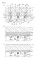
- FIG. 10 is a flowchart for describing a method of manufacturing the semiconductor device.
- FIG. 11 is a diagram for describing a step of forming an inclined surface at an upper edge.
- FIG. 12 is a diagram for describing a step of forming a circular surface at an upper edge.
- FIGS. 1 ( a ) and 1 ( b ) are schematic plan views of a semiconductor device according to a embodiment of the present invention, where FIG. 1 ( a ) is an overall view and FIG. 1 ( b ) is an enlarged interior view.
- a semiconductor device 1 includes a power MOSFET (Metal-Oxide-Semiconductor Field Effect Transistor) element (individual element) using SiC (silicon carbide) and has a vertical length of about 1 mm in the sheet of FIG. 1 , for example.
- MOSFET Metal-Oxide-Semiconductor Field Effect Transistor
- the semiconductor device 1 includes an active region 3 and an outer circumferential region 4 .
- the active region 3 is configured to act as a field effect transistor and is placed at a center portion on an SiC substrate 2 as an example of a semiconductor layer
- the outer circumferential region 4 as an inactive region, surrounds the active region 3 .
- a source pad 5 including aluminum, for example, is formed to cover a substantially entire region of the active region 3 .
- the source pad 5 is of squared shape in a plan view.
- a removal region 6 surrounding a central region of the source pad 5 is formed along the outer circumferential region 4 .
- a portion of the removal region 6 is selectively recessed toward the central region of the source pad 5 .
- a gate pad 7 is disposed in the recess.
- a pair of gate fingers 8 are formed in a shape symmetrical to the gate pad 7 .
- a gate trench 9 is formed on the SiC substrate 2 .
- the gate trench 9 is disposed directly beneath the source pad 5 , etc.
- the gate trench 9 is formed across the active region 3 and the outer circumferential region 4 .
- the gate trench 9 includes an active trench 91 that is formed to have a lattice shape in the active region 3 and that is configured to be used as a gate of an MOSFET, and a contact trench 92 that is formed to have a stripe shape pulled from each end of the active trench 91 to the outer circumferential region 4 and that is configured to act as a contact to a gate electrode 15 (described later) within the active trench 91 .
- the contact trench 92 is arranged by an extended portion of the active trench 91 .
- the patterns of the active trench 91 and the contact trench 92 are not limited to these shapes, etc.
- the active trench 91 may have a stripe shape and a honeycomb shape.
- the contact trench 92 may have a lattice shape and a honeycomb shape, etc.
- the active region 3 is divided by the active trench 91 into a larger number of unit cells 10 .
- the large number of unit cells 10 are arrayed regularly in a matrix.
- a p + -type channel contact layer 11 is formed at a central region thereof, and an n + -type source layer 12 is formed to surround the p + -type channel contact layer 11 .
- the n + -type source layer 12 forms a side surface of each unit cell 10 (side surface of the active trench 91 ).
- the gate finger 8 is laid along a direction to cross the stripe-shaped contact trench 92 .
- the gate finger 8 is laid in a region inside of a longitudinal direction terminal portion (end portion on the opposite side of the active trench 91 ) of the contact trench 92 , and the terminal portion of the contact trench 92 protrudes outwardly of the gate finger 8 .
- a lower step portion 13 is dug down. The lower step portion 13 is formed throughout the whole of the outer circumferential region 4 .
- FIGS. 2 ( a ) , 2 ( b ), and 2 ( c ) are each cross-sectional views of the semiconductor device, where FIG. 2 ( a ) is a cross-sectional view taken along a cutting plane line IIa-IIa in FIG. 1 ( b ) , FIG. 2 ( b ) is a cross-sectional view taken along a cutting plane line IIb-IIb in FIG. 1 ( b ) , and FIG. 2 ( c ) is a cross-sectional view taken along a cutting plane line IIc-IIc in FIG. 1 ( b ) .
- the semiconductor device 1 includes the SiC substrate 2 .
- the SiC substrate 2 is an n-type, that is, a first conductive type, and is configured to act as a drain region (drift layer) of a field effect transistor.
- a p-type channel layer 14 is formed on a surface 21 side of the SiC substrate 2 .
- the n + -type source layer 12 and the p + -type channel contact layer 11 as an example of a second conductive-type impurity region are formed.
- the p + -type channel contact layer 11 is surrounded by the n + -type source layer 12 .
- the n + -type source layer 12 and the p + -type channel contact layer 11 are both exposed to the surface 21 of the SiC substrate 2 .
- the gate trench 9 is formed on a surface 21 side of the SiC substrate 2 .
- the gate trench 9 penetrates through the n + -type source layer 12 and the p-type channel layer 14 to reach a lower portion of the SiC substrate 2 which is for acting as the drain region of the semiconductor device.
- the p-type channel layer 14 is divided into the large number of unit cells 10 arrayed in lattice, for example.
- a gate insulating film 16 is interposed between the gate electrode 15 and the SiC substrate 2 .
- the gate electrode 15 is embedded in the gate trench 9 (active trench 91 ) up to the surface 21 of the SiC substrate 2 , in the active region 3 , as shown by an oblique hatching in FIG. 1 ( b ) , for example.
- the gate electrode 15 also is formed in a lattice shape, and the upper surface of each unit cell 10 is not covered with the gate electrode 15 and is exposed.
- the gate electrode 15 in the outer circumferential region 4 , has an overlap portion 17 covering from an opening end of the gate trench 9 (contact trench 92 ) to the surface 21 of the SiC substrate 2 .
- the overlap portion 17 crosses the stripe-shaped contact trench 92 along the gate finger 8 , in the embodiment.
- the gate insulating film 16 integrally includes a side-surface insulating film 18 on the side surface of the gate trench 9 , a bottom-surface insulating film 19 on the bottom surface, and a planar insulating film 20 on the surface 21 of the SiC substrate 2 .
- the planar insulating film 20 is interposed at least between the overlap portion 17 and the surface 21 of the SiC substrate 2 .
- the gate electrode 15 is straddled between the n + -type source layer 12 and the lower portion of SiC substrate 2 and is configured to control the formation of an inversion layer (channel) on the surface of the p-type channel layer 14 (side surface of the active trench 91 ). That is, the semiconductor device 1 includes a so-called trench gate type structured MOSFET.
- a p-type pillar layer 22 is formed within the lower portion of the SiC substrate 2 .
- the p-type pillar layer 22 is formed in an inner region of the p-type channel layer 14 of each unit cell 10 . More specifically, in this embodiment, the p-type pillar layer 22 is formed in a shape similar to, for example, the p-type channel layer 14 (in a quadrilateral shape in a plan view in the layout of FIG. 1( b ) ) in approximately the central region of the p-type channel layer 14 .
- the p-type pillar layer 22 is formed to continue to the p-type channel layer 14 and extends toward the back surface of the SiC substrate 2 to a depth greater than the p-type channel layer 14 . That is, the p-type pillar layer 22 is formed in an approximately pillar shape (in an approximately quadrangular prism shape in the layout of FIG. 1 ( b ) ). Thus, on the SiC substrate 2 , the p-type pillar layers 22 arrayed at a suitable pitch and the SiC substrate 2 for acting as the n-type drain region sandwiched between the respectively adjacent p type pillar layers 22 are alternatingly arrayed in a direction along the surface 21 .
- a contact hole 24 is selectively formed in the central region of the p-type channel layer 14 .
- the contact hole 24 is formed in a region allowing for selective exposure of one portion of the p + -type channel contact layer 11 and n + -type source layer 12 therearound.
- a contact hole 25 is selectively formed directly beneath the gate finger 8 in the embodiment, the contact hole 25 is formed linearly to surround the active region 3 along the outer circumferential region 4 in the width direction center of the gate finger 8 .
- the source pad 5 and the gate finger 8 are formed on the interlayer film 23 .
- the source pad 5 integrally enters into all the contact holes 24 , and is connected to the n + -type source layer 12 and the p + -type channel contact layer 11 in each unit cell 10 . Therefore, the n + -type source layer 12 is the same in electrical potential as the source pad 5 .
- the p-type channel layer 14 is connected via the p + -type channel contact layer 11 to the source pad 5 , and thus, the same in electrical potential as the source pad 5 .
- the gate finger 8 enters into the contact hole 25 and is connected to the overlap portion 17 of the gate electrode 15 . Therefore, the gate electrode 15 embedded in the active trench 91 is connected via the overlap portion 17 to the gate finger 8 , and thus, the same in electrical potential as the gate finger 8 (gate pad 7 ).
- the overlap portion 17 of the gate electrode 15 also is thereby applied the on-voltage.
- the electric field generated from the overlap portion 17 concentrates at the upper edge of the contact trench 92 .
- the gate insulating film 16 may experience dielectric breakdown. Therefore, the inventors of the present application found a structure shown in FIG. 3 to FIG. 9 as a structure enabling prevention of the dielectric breakdown of such gate insulating film 16 .
- FIG. 3 to FIG. 9 each are a cross-sectional view showing first to seventh embodiments of the gate finger portion of the semiconductor device.
- identical reference signs are allotted to portions corresponding to each portion shown in the figures before FIG. 4 to FIG. 9 .
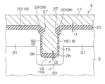
- the side-surface insulating film 18 includes the overhung portion 27 selectively thicker than other portions of the side-surface insulating film 18 so as to protrude inwardly of the contact trench 92 at the upper edge 26 of the contact trench 92 .
- the upper edge 26 is a corner portion including a nodal line formed when the side surface of the contact trench 92 and the surface 21 of the SiC substrate 2 cross.
- This provision of the overhung portion 27 enables improvement of withstand voltage of the gate insulating film 16 at the upper edge 26 .
- the electric field is concentrated at the upper edge 26 when the gate is turned on, it is possible to prevent a dielectric breakdown of the gate insulating film 16 at the upper edge 26 .
- a thickness t 2 of the bottom-surface insulating film 19 is equal to or more than a thickness t 1 of the planar insulating film 20 (t 2 ⁇ t 1 ), and both of the thicknesses t 1 and t 2 are more than a thickness t 3 of the side-surface insulating film 18 (other than the overhung portion 27 ). That is, a relationship of t 2 ⁇ t 1 >t 3 is satisfied.
- the arrangement enables a reduction in the capacitance of a capacitor arranged by the gate electrode 15 and the SiC substrate 2 for acting as the n-type drain region, that face each other with the bottom-surface insulating film 19 being interposed therebetween. As a result, it is possible to reduce the capacity of the entire gate (gate capacitance). Further, it is possible to improve the withstand voltage of the bottom-surface insulating film 19 , and thus, it is also possible to prevent a dielectric breakdown of the bottom-surface insulating film 19 when the gate is turned off.
- the planar insulating film 20 is also thick, and thus, it is possible to reduce the capacitance of a capacitor arranged by the gate electrode 15 (overlap portion 17 ) and the SiC substrate 2 that acts as the n-type drain region, that face each other with the planar insulating film 20 being interposed therebetween. As a result, it is possible to reduce the capacity of the entire gate (gate capacitance).
- the lower edge on the bottom portion of the contact trench 92 is the circular surface 28 allowing continuation between the side surface and the bottom surface of the contact trench 92 . That is, the lower edge of the contact trench 92 is not sharp, but rounded by the circular surface 28 .
- the upper edge 26 of the contact trench 92 includes, in addition to the arrangement in FIG. 3 , an inclined surface 29 allowing the continuation between the surface 21 of the SiC substrate 2 and the side surface of the contact trench 92 . That is, the upper edge 26 of the contact trench 92 is in a chamfered shape.
- the upper edge 26 of the contact trench 92 includes, in addition to the arrangement in FIG. 3 , a circular surface 30 allowing the continuation between the surface 21 of the SiC substrate 2 and the side surface of the contact trench 92 . That is, the upper edge 26 of the contact trench 92 is not sharp, but rounded by the circular surface 30 .
- a p-type layer 31 is formed at the surface 21 side of the SiC substrate 2 .
- the p-type layer 31 has the same depth as the p-type channel layer 14 (see FIG. 2 ( a ) ) in the active region 3 .
- an n + -type layer 32 is formed within the p-type layer 31 .
- the n + -type layer 32 has the same depth as the n + -type source layer 12 (see FIG. 2 ( a ) ) in the active region 3 .
- a bottom portion p-type layer 33 is formed in the SiC substrate 2 .
- the bottom portion p-type layer 33 has the same depth as the p-type pillar layer 22 in the active region 3 in a manner continuing to the p-type layer 31 .
- the bottom portion p-type layer 33 is formed on the bottom surface and the side surface of the contact trench 92 so that the SiC substrate 2 is hidden below the p-type layer 31 .
- the bottom portion p-type layer 33 is continued to the p-type layer 31 on the side surface of the contact trench 92 .
- the bottom portion p-type layer 33 may be combined with the arrangement in FIG. 7 , as in the seventh embodiment shown in FIG. 9 .
- the overhung portion 27 , the circular surface 28 , the inclined surface 29 , and the circular surface 30 shown in FIG. 3 to FIG. 9 may also be formed in the active trench 91 .
- FIG. 10 is a flowchart for describing the method of manufacturing a semiconductor device.
- an impurity is selectively implanted in the surface 21 of the SiC substrate 2 , for example, to perform annealing treatment (step S 1 ).
- an impurity region of the p-type channel layer 14 , the n + -type source layer 12 , and the p + -type channel contact layer 11 , etc. is formed.
- the gate trench 9 the active trench 91 and the contact trench 92 ) is formed on the SiC substrate 2 (step S 2 ).
- a next step is to form the gate insulating film 16 (step S 3 ).
- a CVD method is used under a predetermined condition (a gas flow rate, types of gas, a gas ratio, a gas supply time, etc.) so as to deposit an insulating material within the gate trench 9 so that the overhung portion 27 selectively thicker than other portions at the upper edge 26 of the contact trench 92 is formed.
- the gate insulating film 16 having the overhung portion 27 is thereby formed.
- the SiC substrate 2 is thermally oxidized.
- the sacrificial oxide film 34 is formed.
- the oxidization is generally started from both the surface 21 of the SiC substrate 2 and the side surface of the contact trench 92 .
- an oxide film that has traveled from the surface 21 of the SiC substrate 2 and an oxide film that has traveled from the side surface of the contact trench 92 are integrated before other regions.
- the inclined surface 29 is formed below the oxide film integrated through the above process.
- the sacrificial oxide film 34 may be removed to form the gate insulating film 16 by using a CVD method.
- the H 2 annealing treatment is performed on the SiC substrate 2 .
- H 2 anneal H 2 etching
- the polysilicon is deposited until the entire gate trench 9 is hidden to fill the gate trench 9 with the polysilicon (step S 4 ). Then, when the deposited polysilicon is patterned, the polysilicon outside the active trench 91 is removed in the active region 3 , and at the same time, the polysilicon is left as the overlap portion 17 in the outer circumferential region 4 .
- step S 5 the interlayer film 23 is formed on the SiC substrate 2 (step S 5 ).
- step S 6 the contact hole 24 and the contact hole 25 are formed simultaneously.
- step S 7 the source pad 5 , the gate pad 7 , and the gate finger 8 are formed.
- the semiconductor device 1 shown in FIG. 1 is obtained.
- the conductive type of each of the semiconductor portions of the forgoing semiconductor device 1 is inverted.
- the p-type portions may be n-type and the n-type portions may be p-type.
- the semiconductor adopted in the semiconductor device 1 may not only be SiC but also be Si, GaN, diamond, etc., for example.
- the overlap portion 17 may be formed not only in the outer circumferential region 4 but also in the active region 3 .
- the overlap portion 17 may also be formed in the active region 3 .
- the overhung portion 27 is formed also in the active trench 91 , then it is possible to obtain the withstand voltage improvement effect in much the same way as in the above. That is, the structure immediately below the gate finger 8 is merely an example exhibiting the effect of the withstand voltage improvement effect by the overhung portion 27 according to the present invention, and thus, a structure capable of obtaining a similar effect may be provided not only to the gate finger portion.
Landscapes
- Engineering & Computer Science (AREA)
- Microelectronics & Electronic Packaging (AREA)
- Power Engineering (AREA)
- Physics & Mathematics (AREA)
- Condensed Matter Physics & Semiconductors (AREA)
- General Physics & Mathematics (AREA)
- Computer Hardware Design (AREA)
- Ceramic Engineering (AREA)
- Manufacturing & Machinery (AREA)
- Chemical & Material Sciences (AREA)
- Crystallography & Structural Chemistry (AREA)
- Electrodes Of Semiconductors (AREA)
Applications Claiming Priority (3)
| Application Number | Priority Date | Filing Date | Title |
|---|---|---|---|
| JP2012103862A JP2013232533A (ja) | 2012-04-27 | 2012-04-27 | 半導体装置および半導体装置の製造方法 |
| JP2012-103862 | 2012-04-27 | ||
| PCT/JP2013/061765 WO2013161753A1 (ja) | 2012-04-27 | 2013-04-22 | 半導体装置および半導体装置の製造方法 |
Publications (2)
| Publication Number | Publication Date |
|---|---|
| US20150295079A1 US20150295079A1 (en) | 2015-10-15 |
| US9536998B2 true US9536998B2 (en) | 2017-01-03 |
Family
ID=49483066
Family Applications (1)
| Application Number | Title | Priority Date | Filing Date |
|---|---|---|---|
| US14/397,073 Active US9536998B2 (en) | 2012-04-27 | 2013-04-22 | Semiconductor device and semiconductor device manufacturing method |
Country Status (5)
| Country | Link |
|---|---|
| US (1) | US9536998B2 (zh) |
| EP (2) | EP3584843B1 (zh) |
| JP (1) | JP2013232533A (zh) |
| CN (3) | CN116013974A (zh) |
| WO (1) | WO2013161753A1 (zh) |
Cited By (1)
| Publication number | Priority date | Publication date | Assignee | Title |
|---|---|---|---|---|
| US20160260832A1 (en) * | 2015-03-06 | 2016-09-08 | Toyoda Gosei Co., Ltd. | Semiconductor device, method of manufacturing the same and power converter |
Families Citing this family (28)
| Publication number | Priority date | Publication date | Assignee | Title |
|---|---|---|---|---|
| JP6112700B2 (ja) * | 2012-08-17 | 2017-04-12 | ローム株式会社 | 半導体装置 |
| JP6098474B2 (ja) * | 2013-10-24 | 2017-03-22 | 住友電気工業株式会社 | 炭化珪素半導体装置およびその製造方法 |
| JP6229443B2 (ja) * | 2013-11-11 | 2017-11-15 | 住友電気工業株式会社 | 炭化珪素半導体装置およびその製造方法 |
| JP6252900B2 (ja) * | 2013-11-29 | 2017-12-27 | 株式会社デンソー | 半導体装置 |
| JP6179409B2 (ja) * | 2014-01-24 | 2017-08-16 | 株式会社デンソー | 炭化珪素半導体装置の製造方法 |
| CN104810268A (zh) * | 2014-01-29 | 2015-07-29 | 北大方正集团有限公司 | 沟槽型功率器件栅氧化层的制备方法 |
| JP6357869B2 (ja) | 2014-05-20 | 2018-07-18 | 住友電気工業株式会社 | 炭化珪素半導体装置の製造方法 |
| JP6256192B2 (ja) | 2014-05-26 | 2018-01-10 | トヨタ自動車株式会社 | 半導体装置 |
| JP6318914B2 (ja) * | 2014-06-30 | 2018-05-09 | 住友電気工業株式会社 | 炭化珪素半導体装置の製造方法および炭化珪素半導体装置 |
| JP6526981B2 (ja) | 2015-02-13 | 2019-06-05 | ローム株式会社 | 半導体装置および半導体モジュール |
| JP6600475B2 (ja) * | 2015-03-27 | 2019-10-30 | ローム株式会社 | 半導体装置 |
| JP2016213419A (ja) * | 2015-05-13 | 2016-12-15 | 住友電気工業株式会社 | 炭化珪素半導体装置 |
| US9461131B1 (en) * | 2015-06-15 | 2016-10-04 | Texas Instruments Incorporated | High quality deep trench oxide |
| US9691759B2 (en) * | 2015-10-01 | 2017-06-27 | Panasonic Intellectual Property Management Co., Ltd. | Semiconductor device including semiconductor substrate, silicon carbide semiconductor layer, unit cells, source, and gate |
| JP6528640B2 (ja) * | 2015-10-22 | 2019-06-12 | 三菱電機株式会社 | 半導体装置及びその製造方法 |
| JP6750969B2 (ja) | 2016-06-23 | 2020-09-02 | ルネサスエレクトロニクス株式会社 | 半導体装置の製造方法 |
| JP2018074126A (ja) | 2016-11-04 | 2018-05-10 | トヨタ自動車株式会社 | 半導体装置 |
| JP6967907B2 (ja) * | 2017-08-07 | 2021-11-17 | ルネサスエレクトロニクス株式会社 | 半導体装置及び半導体装置の製造方法 |
| DE102017118121B4 (de) * | 2017-08-09 | 2019-08-14 | Infineon Technologies Austria Ag | Halbleiterbauelement und Herstellungsverfahren dafür |
| CN111684607A (zh) | 2018-01-17 | 2020-09-18 | 罗姆股份有限公司 | 半导体装置及其制造方法 |
| WO2019176327A1 (ja) * | 2018-03-15 | 2019-09-19 | 富士電機株式会社 | 半導体装置 |
| JP7175864B2 (ja) * | 2019-09-17 | 2022-11-21 | 株式会社東芝 | 半導体装置 |
| JP6876767B2 (ja) * | 2019-10-07 | 2021-05-26 | ローム株式会社 | 半導体装置 |
| JP7400487B2 (ja) | 2020-01-17 | 2023-12-19 | 富士電機株式会社 | 半導体装置 |
| US11222955B2 (en) * | 2020-04-22 | 2022-01-11 | Wolfspeed, Inc. | Semiconductor power devices having gate dielectric layers with improved breakdown characteristics and methods of forming such devices |
| JP7256254B2 (ja) * | 2020-10-02 | 2023-04-11 | ローム株式会社 | 半導体装置 |
| WO2022209089A1 (ja) * | 2021-03-29 | 2022-10-06 | 住友電気工業株式会社 | 炭化珪素半導体装置 |
| CN116632035A (zh) * | 2023-04-25 | 2023-08-22 | 海信家电集团股份有限公司 | 半导体装置及其制作方法 |
Citations (28)
| Publication number | Priority date | Publication date | Assignee | Title |
|---|---|---|---|---|
| US5072266A (en) | 1988-12-27 | 1991-12-10 | Siliconix Incorporated | Trench DMOS power transistor with field-shaping body profile and three-dimensional geometry |
| JPH07249769A (ja) | 1994-01-20 | 1995-09-26 | Mitsubishi Electric Corp | トレンチ構造を有する半導体装置およびその製造方法 |
| EP0676814A2 (en) | 1994-04-06 | 1995-10-11 | Nippondenso Co., Ltd. | Trench semiconductor device and process of producing same |
| JPH09307101A (ja) | 1996-05-15 | 1997-11-28 | Toyota Central Res & Dev Lab Inc | 半導体装置およびその製造方法 |
| US5723376A (en) | 1994-06-23 | 1998-03-03 | Nippondenso Co., Ltd. | Method of manufacturing SiC semiconductor device having double oxide film formation to reduce film defects |
| JPH10154810A (ja) | 1996-11-25 | 1998-06-09 | Sanyo Electric Co Ltd | 半導体装置及び半導体装置の製造方法 |
| JPH10200104A (ja) | 1997-01-13 | 1998-07-31 | Hitachi Ltd | 電圧駆動型半導体装置及びその製造方法 |
| JP2001127284A (ja) | 1999-10-26 | 2001-05-11 | Hitachi Ltd | 半導体装置の製造方法 |
| US20010008291A1 (en) * | 2000-01-14 | 2001-07-19 | Takaaki Aoki | Semiconductor device and method for manufacturing the same |
| US6303460B1 (en) * | 2000-02-07 | 2001-10-16 | Mitsubishi Denki Kabushiki Kaisha | Semiconductor device and method for manufacturing the same |
| US6455378B1 (en) | 1999-10-26 | 2002-09-24 | Hitachi, Ltd. | Method of manufacturing a trench gate power transistor with a thick bottom insulator |
| US20020167046A1 (en) | 2000-01-14 | 2002-11-14 | Takaaki Aoki | Semiconductor device and method for manufacturing the same |
| US20040173844A1 (en) | 2003-03-05 | 2004-09-09 | Advanced Analogic Technologies, Inc. Advanced Analogic Technologies (Hongkong) Limited | Trench power MOSFET with planarized gate bus |
| US20040195618A1 (en) | 2003-04-07 | 2004-10-07 | Wataru Saito | Insulated gate semiconductor device |
| US6825087B1 (en) * | 1999-11-24 | 2004-11-30 | Fairchild Semiconductor Corporation | Hydrogen anneal for creating an enhanced trench for trench MOSFETS |
| US20050263852A1 (en) * | 2004-05-28 | 2005-12-01 | Kabushiki Kaisha Toshiba | Semiconductor device |
| US20060160306A1 (en) | 2005-01-17 | 2006-07-20 | Min-San Huang | Method for forming trench gate dielectric layer |
| JP2007048769A (ja) | 2005-08-05 | 2007-02-22 | Matsushita Electric Ind Co Ltd | 半導体装置およびその製造方法 |
| US20070075362A1 (en) | 2005-09-30 | 2007-04-05 | Ching-Yuan Wu | Self-aligned schottky-barrier clamped trench DMOS transistor structure and its manufacturing methods |
| JP2009071009A (ja) | 2007-09-13 | 2009-04-02 | Hitachi Ltd | 半導体装置及びその製造方法 |
| US20100193862A1 (en) | 2009-02-05 | 2010-08-05 | Nec Electronics Corporation | Semiconductor device and method of manufacturing the same |
| WO2010119789A1 (ja) | 2009-04-13 | 2010-10-21 | ローム株式会社 | 半導体装置および半導体装置の製造方法 |
| JP2010245256A (ja) | 2009-04-06 | 2010-10-28 | Renesas Electronics Corp | 半導体装置およびその製造方法 |
| US20110018004A1 (en) | 2009-07-21 | 2011-01-27 | Hitachi, Ltd. | Semiconductor device with large blocking voltage and manufacturing method thereof |
| US20110291110A1 (en) | 2010-05-31 | 2011-12-01 | Toyota Jidosha Kabushiki Kaisha | Silicon carbide semiconductor device and method of manufacturing the same |
| US20120052642A1 (en) | 2010-08-31 | 2012-03-01 | Toyota Jidosha Kabushiki Kaisha | Method of manufacturing silicon carbide semiconductor device |
| US20120261746A1 (en) * | 2011-03-14 | 2012-10-18 | Maxpower Semiconductor, Inc. | Double-Trench Vertical Devices and Methods with Self-Alignment Between Gate and Body Contact |
| US20120261714A1 (en) * | 2011-04-12 | 2012-10-18 | Denso Corporation | Semiconductor device and manufacturing method of the same |
Family Cites Families (8)
| Publication number | Priority date | Publication date | Assignee | Title |
|---|---|---|---|---|
| JP3307785B2 (ja) * | 1994-12-13 | 2002-07-24 | 三菱電機株式会社 | 絶縁ゲート型半導体装置 |
| EP1009035B1 (en) * | 1997-08-29 | 2004-07-21 | Mitsubishi Denki Kabushiki Kaisha | Insulated gate semiconductor device and method for manufacturing the same |
| US6838722B2 (en) * | 2002-03-22 | 2005-01-04 | Siliconix Incorporated | Structures of and methods of fabricating trench-gated MIS devices |
| JP2006049341A (ja) * | 2004-07-30 | 2006-02-16 | Renesas Technology Corp | 半導体装置およびその製造方法 |
| JP4840482B2 (ja) * | 2008-10-14 | 2011-12-21 | 株式会社デンソー | 半導体装置 |
| US8546814B2 (en) * | 2009-03-25 | 2013-10-01 | Rohm Co., Ltd. | Semiconductor device |
| US9105715B2 (en) * | 2009-04-30 | 2015-08-11 | Mitsubishi Electric Corporation | Semiconductor device and method for manufacturing the same |
| JP2011210916A (ja) * | 2010-03-30 | 2011-10-20 | Mitsumi Electric Co Ltd | 半導体装置の製造方法 |
-
2012
- 2012-04-27 JP JP2012103862A patent/JP2013232533A/ja active Pending
-
2013
- 2013-04-22 CN CN202310046900.9A patent/CN116013974A/zh active Pending
- 2013-04-22 CN CN201380022113.5A patent/CN104247028B/zh active Active
- 2013-04-22 CN CN201810083012.3A patent/CN108155087B/zh active Active
- 2013-04-22 WO PCT/JP2013/061765 patent/WO2013161753A1/ja active Application Filing
- 2013-04-22 US US14/397,073 patent/US9536998B2/en active Active
- 2013-04-22 EP EP19188674.6A patent/EP3584843B1/en active Active
- 2013-04-22 EP EP13781066.9A patent/EP2843707B1/en active Active
Patent Citations (40)
| Publication number | Priority date | Publication date | Assignee | Title |
|---|---|---|---|---|
| US5072266A (en) | 1988-12-27 | 1991-12-10 | Siliconix Incorporated | Trench DMOS power transistor with field-shaping body profile and three-dimensional geometry |
| JPH07249769A (ja) | 1994-01-20 | 1995-09-26 | Mitsubishi Electric Corp | トレンチ構造を有する半導体装置およびその製造方法 |
| US5541425A (en) | 1994-01-20 | 1996-07-30 | Mitsubishi Denki Kabushiki Kaisha | Semiconductor device having trench structure |
| US5795792A (en) | 1994-01-20 | 1998-08-18 | Mitsubishi Denki Kabushiki Kaisha | Method of manufacturing a semiconductor device having a trench structure |
| EP0676814A2 (en) | 1994-04-06 | 1995-10-11 | Nippondenso Co., Ltd. | Trench semiconductor device and process of producing same |
| US5723376A (en) | 1994-06-23 | 1998-03-03 | Nippondenso Co., Ltd. | Method of manufacturing SiC semiconductor device having double oxide film formation to reduce film defects |
| JPH09307101A (ja) | 1996-05-15 | 1997-11-28 | Toyota Central Res & Dev Lab Inc | 半導体装置およびその製造方法 |
| JPH10154810A (ja) | 1996-11-25 | 1998-06-09 | Sanyo Electric Co Ltd | 半導体装置及び半導体装置の製造方法 |
| JPH10200104A (ja) | 1997-01-13 | 1998-07-31 | Hitachi Ltd | 電圧駆動型半導体装置及びその製造方法 |
| US6455378B1 (en) | 1999-10-26 | 2002-09-24 | Hitachi, Ltd. | Method of manufacturing a trench gate power transistor with a thick bottom insulator |
| JP2001127284A (ja) | 1999-10-26 | 2001-05-11 | Hitachi Ltd | 半導体装置の製造方法 |
| US6825087B1 (en) * | 1999-11-24 | 2004-11-30 | Fairchild Semiconductor Corporation | Hydrogen anneal for creating an enhanced trench for trench MOSFETS |
| US20010008291A1 (en) * | 2000-01-14 | 2001-07-19 | Takaaki Aoki | Semiconductor device and method for manufacturing the same |
| US20020167046A1 (en) | 2000-01-14 | 2002-11-14 | Takaaki Aoki | Semiconductor device and method for manufacturing the same |
| US6303460B1 (en) * | 2000-02-07 | 2001-10-16 | Mitsubishi Denki Kabushiki Kaisha | Semiconductor device and method for manufacturing the same |
| US20060014349A1 (en) | 2003-03-05 | 2006-01-19 | Williams Richard K | Planarized and silicided trench contact |
| US20040183136A1 (en) | 2003-03-05 | 2004-09-23 | Williams Richard K. | Planarized and silicided trench contact |
| US20040183129A1 (en) | 2003-03-05 | 2004-09-23 | Williams Richard K. | Poly-sealed silicide trench gate |
| WO2004079794A2 (en) | 2003-03-05 | 2004-09-16 | Advanced Analogic Technologies Inc. | Trench power mosfet with planarized gate bus |
| JP2010118701A (ja) | 2003-03-05 | 2010-05-27 | Advanced Analogic Technologies Inc | トレンチゲート縦型mosfet |
| JP2006520091A (ja) | 2003-03-05 | 2006-08-31 | アドバンスト・アナロジック・テクノロジーズ・インコーポレイテッド | 平坦化したゲートバスを備えたトレンチ・パワーmosfet |
| US20040173844A1 (en) | 2003-03-05 | 2004-09-09 | Advanced Analogic Technologies, Inc. Advanced Analogic Technologies (Hongkong) Limited | Trench power MOSFET with planarized gate bus |
| US20040195618A1 (en) | 2003-04-07 | 2004-10-07 | Wataru Saito | Insulated gate semiconductor device |
| JP2004311716A (ja) | 2003-04-07 | 2004-11-04 | Toshiba Corp | 絶縁ゲート型半導体装置 |
| US20050263852A1 (en) * | 2004-05-28 | 2005-12-01 | Kabushiki Kaisha Toshiba | Semiconductor device |
| US20060160306A1 (en) | 2005-01-17 | 2006-07-20 | Min-San Huang | Method for forming trench gate dielectric layer |
| JP2007048769A (ja) | 2005-08-05 | 2007-02-22 | Matsushita Electric Ind Co Ltd | 半導体装置およびその製造方法 |
| US20070075362A1 (en) | 2005-09-30 | 2007-04-05 | Ching-Yuan Wu | Self-aligned schottky-barrier clamped trench DMOS transistor structure and its manufacturing methods |
| JP2009071009A (ja) | 2007-09-13 | 2009-04-02 | Hitachi Ltd | 半導体装置及びその製造方法 |
| US20100193862A1 (en) | 2009-02-05 | 2010-08-05 | Nec Electronics Corporation | Semiconductor device and method of manufacturing the same |
| JP2010182857A (ja) | 2009-02-05 | 2010-08-19 | Renesas Electronics Corp | 半導体装置およびその製造方法 |
| JP2010245256A (ja) | 2009-04-06 | 2010-10-28 | Renesas Electronics Corp | 半導体装置およびその製造方法 |
| US20120049202A1 (en) * | 2009-04-13 | 2012-03-01 | Rohm Co., Ltd | Semiconductor device and method of manufacturing semiconductor device |
| WO2010119789A1 (ja) | 2009-04-13 | 2010-10-21 | ローム株式会社 | 半導体装置および半導体装置の製造方法 |
| US20110018004A1 (en) | 2009-07-21 | 2011-01-27 | Hitachi, Ltd. | Semiconductor device with large blocking voltage and manufacturing method thereof |
| JP2011253837A (ja) | 2010-05-31 | 2011-12-15 | Denso Corp | 炭化珪素半導体装置およびその製造方法 |
| US20110291110A1 (en) | 2010-05-31 | 2011-12-01 | Toyota Jidosha Kabushiki Kaisha | Silicon carbide semiconductor device and method of manufacturing the same |
| US20120052642A1 (en) | 2010-08-31 | 2012-03-01 | Toyota Jidosha Kabushiki Kaisha | Method of manufacturing silicon carbide semiconductor device |
| US20120261746A1 (en) * | 2011-03-14 | 2012-10-18 | Maxpower Semiconductor, Inc. | Double-Trench Vertical Devices and Methods with Self-Alignment Between Gate and Body Contact |
| US20120261714A1 (en) * | 2011-04-12 | 2012-10-18 | Denso Corporation | Semiconductor device and manufacturing method of the same |
Non-Patent Citations (2)
| Title |
|---|
| Extended Search Report issued in counterpart European patent application No. 13781066.9, Nov. 4, 2015 (10 pages). |
| International Preliminary Report on Patentability and Written Opinion; PCT/JP2013/061765 (6 pages). |
Cited By (1)
| Publication number | Priority date | Publication date | Assignee | Title |
|---|---|---|---|---|
| US20160260832A1 (en) * | 2015-03-06 | 2016-09-08 | Toyoda Gosei Co., Ltd. | Semiconductor device, method of manufacturing the same and power converter |
Also Published As
| Publication number | Publication date |
|---|---|
| JP2013232533A (ja) | 2013-11-14 |
| WO2013161753A1 (ja) | 2013-10-31 |
| CN108155087A (zh) | 2018-06-12 |
| EP3584843A1 (en) | 2019-12-25 |
| EP2843707A1 (en) | 2015-03-04 |
| US20150295079A1 (en) | 2015-10-15 |
| CN108155087B (zh) | 2023-01-10 |
| EP2843707A4 (en) | 2015-12-02 |
| CN104247028B (zh) | 2018-03-06 |
| CN104247028A (zh) | 2014-12-24 |
| EP3584843B1 (en) | 2023-03-29 |
| EP2843707B1 (en) | 2019-08-28 |
| CN116013974A (zh) | 2023-04-25 |
Similar Documents
| Publication | Publication Date | Title |
|---|---|---|
| US9536998B2 (en) | Semiconductor device and semiconductor device manufacturing method | |
| US11888058B2 (en) | Semiconductor device | |
| US9337298B2 (en) | Silicon carbide semiconductor device and method for producing the same | |
| CN103928516B (zh) | 具有双平行沟道结构的半导体器件及其制造方法 | |
| US9508803B2 (en) | Semiconductor device and method for producing semiconductor device | |
| JP6876767B2 (ja) | 半導体装置 | |
| JP2023165988A (ja) | 半導体装置 | |
| JP6273329B2 (ja) | 半導体装置 | |
| JP2018085531A (ja) | 半導体装置 | |
| EP3200236A1 (en) | Silicon carbide semiconductor device, method for manufacturing silicon carbide semiconductor device, and method for designing silicon carbide semiconductor device | |
| CN118099190A (zh) | 半导体装置 |
Legal Events
| Date | Code | Title | Description |
|---|---|---|---|
| AS | Assignment |
Owner name: ROHM CO., LTD., JAPAN Free format text: ASSIGNMENT OF ASSIGNORS INTEREST;ASSIGNORS:NAKANO, YUKI;NAKAMURA, RYOTA;SAKAIRI, HIROYUKI;REEL/FRAME:034033/0663 Effective date: 20141010 |
|
| STCF | Information on status: patent grant |
Free format text: PATENTED CASE |
|
| MAFP | Maintenance fee payment |
Free format text: PAYMENT OF MAINTENANCE FEE, 4TH YEAR, LARGE ENTITY (ORIGINAL EVENT CODE: M1551); ENTITY STATUS OF PATENT OWNER: LARGE ENTITY Year of fee payment: 4 |