US9153752B2 - Method of manufacturing light-emitting device - Google Patents
Method of manufacturing light-emitting device Download PDFInfo
- Publication number
- US9153752B2 US9153752B2 US13/817,320 US201113817320A US9153752B2 US 9153752 B2 US9153752 B2 US 9153752B2 US 201113817320 A US201113817320 A US 201113817320A US 9153752 B2 US9153752 B2 US 9153752B2
- Authority
- US
- United States
- Prior art keywords
- light
- liquid mixture
- emitting element
- nozzle
- manufacturing
- Prior art date
- Legal status (The legal status is an assumption and is not a legal conclusion. Google has not performed a legal analysis and makes no representation as to the accuracy of the status listed.)
- Active
Links
Images


Classifications
-
- H—ELECTRICITY
- H10—SEMICONDUCTOR DEVICES; ELECTRIC SOLID-STATE DEVICES NOT OTHERWISE PROVIDED FOR
- H10H—INORGANIC LIGHT-EMITTING SEMICONDUCTOR DEVICES HAVING POTENTIAL BARRIERS
- H10H20/00—Individual inorganic light-emitting semiconductor devices having potential barriers, e.g. light-emitting diodes [LED]
- H10H20/80—Constructional details
- H10H20/85—Packages
- H10H20/851—Wavelength conversion means
- H10H20/8511—Wavelength conversion means characterised by their material, e.g. binder
- H10H20/8512—Wavelength conversion materials
-
- H01L33/502—
-
- H—ELECTRICITY
- H01—ELECTRIC ELEMENTS
- H01L—SEMICONDUCTOR DEVICES NOT COVERED BY CLASS H10
- H01L22/00—Testing or measuring during manufacture or treatment; Reliability measurements, i.e. testing of parts without further processing to modify the parts as such; Structural arrangements therefor
- H01L22/10—Measuring as part of the manufacturing process
-
- H01L33/005—
-
- H01L33/50—
-
- H01L33/52—
-
- H01L33/56—
-
- H—ELECTRICITY
- H10—SEMICONDUCTOR DEVICES; ELECTRIC SOLID-STATE DEVICES NOT OTHERWISE PROVIDED FOR
- H10H—INORGANIC LIGHT-EMITTING SEMICONDUCTOR DEVICES HAVING POTENTIAL BARRIERS
- H10H20/00—Individual inorganic light-emitting semiconductor devices having potential barriers, e.g. light-emitting diodes [LED]
- H10H20/01—Manufacture or treatment
- H10H20/011—Manufacture or treatment of bodies, e.g. forming semiconductor layers
- H10H20/013—Manufacture or treatment of bodies, e.g. forming semiconductor layers having light-emitting regions comprising only Group III-V materials
- H10H20/0137—Manufacture or treatment of bodies, e.g. forming semiconductor layers having light-emitting regions comprising only Group III-V materials the light-emitting regions comprising nitride materials
-
- H—ELECTRICITY
- H10—SEMICONDUCTOR DEVICES; ELECTRIC SOLID-STATE DEVICES NOT OTHERWISE PROVIDED FOR
- H10H—INORGANIC LIGHT-EMITTING SEMICONDUCTOR DEVICES HAVING POTENTIAL BARRIERS
- H10H20/00—Individual inorganic light-emitting semiconductor devices having potential barriers, e.g. light-emitting diodes [LED]
- H10H20/80—Constructional details
- H10H20/85—Packages
- H10H20/851—Wavelength conversion means
- H10H20/8511—Wavelength conversion means characterised by their material, e.g. binder
-
- H—ELECTRICITY
- H10—SEMICONDUCTOR DEVICES; ELECTRIC SOLID-STATE DEVICES NOT OTHERWISE PROVIDED FOR
- H10H—INORGANIC LIGHT-EMITTING SEMICONDUCTOR DEVICES HAVING POTENTIAL BARRIERS
- H10H20/00—Individual inorganic light-emitting semiconductor devices having potential barriers, e.g. light-emitting diodes [LED]
- H10H20/80—Constructional details
- H10H20/85—Packages
- H10H20/852—Encapsulations
- H10H20/854—Encapsulations characterised by their material, e.g. epoxy or silicone resins
-
- H01L2933/0041—
-
- H—ELECTRICITY
- H10—SEMICONDUCTOR DEVICES; ELECTRIC SOLID-STATE DEVICES NOT OTHERWISE PROVIDED FOR
- H10H—INORGANIC LIGHT-EMITTING SEMICONDUCTOR DEVICES HAVING POTENTIAL BARRIERS
- H10H20/00—Individual inorganic light-emitting semiconductor devices having potential barriers, e.g. light-emitting diodes [LED]
- H10H20/01—Manufacture or treatment
- H10H20/036—Manufacture or treatment of packages
- H10H20/0361—Manufacture or treatment of packages of wavelength conversion means
Definitions
- the present invention relates to a method of manufacturing a light-emitting device.
- Patent Document 1 discloses that settlement or segregation of a fluorescent substance can be suppressed by using a silicone resin as a sealant, which resin has a viscosity of from 100 to 1000 cP when it hardens.
- Patent Document 2 discloses a chip-part type LED configured such that LED elements are arranged between the upper end opening and the bottom end opening of a cylindrical container, the cylindrical container is filled with a translucent resin from the upper end opening to the bottom end opening, and the inner face of the container is formed so as to reflect light emitted from the LED element to the upper end opening.
- Patent Document 3 discloses a light-emitting device composed of a liquid translucent sealant material and a lipophilic compound added thereto as an anti-settlement agent, which compound prepared by adding organic cations to a layered compound mainly composed of a clay mineral, and discloses a manufacturing method thereof.
- Patent Document 1 Japanese Patent Application Publication No. 2002-314142.
- Patent Document 2 Japanese Patent Application Publication No. 2002-185046.
- Patent Document 3 Japanese Patent Application Publication No. 2004-153109.
- Patent Document 1 since LED chips are sealed with a silicone resin, deterioration of a sealant material such as coloration is easily developed by light emitted from the LED chips, heat generated by the LED chips and the fluorescent substance, and the like. Thus, it is difficult to achieve durability for a long-term use. Further, as for the configuration of Patent Document 2, the structure of LED is complex, which causes a cost increase. Still further, in Patent Documents 2 and 3, resin materials such as an epoxy resin, a silicone resin, and a polyimide resin are described as exemplary translucent sealant materials, but these resins are not adequate in terms of durability of a sealant material, like Patent Document 1.
- LED chips can be sealed with a sealant material which is turned into ceramic after heated.
- a sealant material which is turned into ceramic after heated.
- the layered compound described in Patent Document 2 is added as a settlement inhibiting agent, a dispersed state of a fluorescent substance is stabilized.
- occurrence of color unevenness can be reduced.
- viscosity of a liquid mixture of the sealant material and the settlement inhibiting agent is small, the fluorescent substance settles before the sealant material hardens, i.e., a settlement-suppressing effect is inefficient.
- a main purpose of the present invention is to provide a method of manufacturing a light-emitting device which includes a wavelength conversion portion where a fluorescent substance is dispersed evenly in a translucent material having a high heat durability.
- a method of manufacturing a light-emitting device including a light-emitting element which emits light of a predetermined wavelength and a wavelength conversion portion including a fluorescent substance which is excited by the light emitted from the light-emitting element to emit (generate) fluorescence of a wavelength different from the predetermined wavelength
- the method includes spraying so as to apply a liquid mixture containing a layered silicate mineral and a translucent ceramic precursor on the light-emitting element from a nozzle while the nozzle is moved relative to the light-emitting element; and forming the wavelength conversion portion by heating the sprayed and applied liquid mixture.
- the fluorescent substance can be applied on the light-emitting element in a well-dispersed state, because the liquid mixture containing the fluorescent substance, the layered silicate mineral, and the ceramic precursor is applied on the light-emitting element.
- the wavelength conversion portion where the fluorescent substance is evenly dispersed in the translucent material having a high heat durability can be formed.
- FIG. 1 This is a cross-sectional view illustrating a schematic configuration of a light-emitting device.
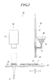
- FIG. 2 This is a schematic diagram for explaining schematically a manufacturing device and a manufacturing method of a light-emitting device.
- a light-emitting device 100 has an LED substrate 1 whose cross-section is concave.
- a metal portion 2 On a concave portion (the bottom portion) of the LED substrate 1 , a metal portion 2 is arranged. Above the metal portion 2 , an LED element 3 in a rectangular shape is arranged.
- the LED element 3 is an example of a light-emitting element which emits light of a predetermined wavelength.
- projecting electrodes 4 are arranged on the surface of the LED element 3 facing to the metal portion 2 .
- the metal portion 2 and the LED element 3 are connected with each other through the projecting electrodes 4 (flip-chip type).
- a plurality of the LED elements 3 can be arranged on the concave portion of one LED substrate 1 .
- a blue LED element is used as the LED element 3 .
- the blue LED element is, for example, constituted of a laminate of an n-GaN cladding layer, an InGaN fluorescent layer, a p-GaN cladding layer and a transparent electrode on a sapphire substrate.
- a wavelength conversion portion 6 is formed so as to seal a surrounding area of the LED element 3 .
- the wavelength conversion portion 6 is a portion which converts light of a predetermined wavelength emitted from the LED element 3 to light of a wavelength different from the emitted light, and where a fluorescent substance which is excited with the wavelength from the LED element 3 and emits fluorescence of a wavelength different from the exciting wavelength is added in a translucent ceramic layer.
- the wavelength conversion portion 6 is formed so as to seal a surrounding area of the LED element 3 in this embodiment, the wavelength conversion portion 6 can be formed just around (on the upper and the side faces of) the LED element 3 , and thus there can be a configuration such that the wavelength conversion portion 6 is not formed on the concave portion of the LED substrate 1 .
- an available method is, for example, placing a mask when the wavelength conversion portion 6 is formed.
- the wavelength conversion portion 6 is a clear ceramic layer (glass body) formed by turning a sol liquid mixture where an organometallic compound is mixed with an organic solvent into a gel by heating followed by firing, which is called the sol-gel method.
- the clear ceramic layer includes the fluorescent substance, the layered silicate mineral, and inorganic fine particles.
- the organometallic compound functions as a binder for sealing the fluorescent substance, the layered silicate mineral, and the inorganic fine particles.
- organometallic compound used in the present invention such as a metal alkoxide, a metal acetylacetonate, a metal carboxylate can be given as the examples.
- a metal alkoxide which is easily turned into a gel by hydrolysis and polymerization, is suitable.
- a metal alcoxide can be monomolecular such as tetraethoxysilane, or can be a polysiloxane constituted of a chain or a ring of organosiloxane compounds.
- a polysiloxane which increases viscosity of the liquid mixture is suitable.
- Types of metals of a metal alkoxide are not limited as long as a translucent glass body can be formed.
- silicon is included in a metal alkoxide.
- a plurality types of metals can be included therein.
- a content of the organometallic compound in the ceramic layer is less than 2% by weight, an amount of the organic compound as a binder is so low that strength of the ceramic layer after heated and fired decreases.
- the content of the organometallic compound in the ceramic layer is more than 50% by weight, a content of the layered silicate mineral become relatively low, and thus viscosity of the liquid mixture decrease and settlement of the fluorescent substance may easily occurs.
- a content of the inorganic fine particles become relatively low, and thus strength of the ceramic layer decreases.
- the content of the organometallic compound in the ceramic layer ranges preferably from 2 to 50% by weight, and more preferably from 2.5 to 30% by weight.
- a polysilazane used in the present invention is represented by the following general formula (1): (R1R2SiNR3) n (1)
- R1, R2 and R3 independently represent hydrogen, an alkyl group, an aryl group, a vinyl group, or a cycloalkyl group. At least one of R1, R2 and R3 is hydrogen, and preferably all of R1, R2 and R3 are hydrogen, and “n” represents an integral number ranging from 1 to 60.
- a Polysilazane can be in any molecular shape, for example, can be a straight chain or a ring.
- a polysilazane represented by the above formula (1) and a reaction accelerating agent as needed are dissolved in an appropriate solvent, and application thereof is performed, and subsequently hardening is performed by heating, excimer light treatment, or UV light treatment.
- a ceramic layer having a high heat and light durability can be formed.
- hardening by irradiation of UVU radiation including light of wavelength of from 170 to 230 nm (for example, excimer light) followed by heat hardening further enhances a water seepage-preventing effect.
- reaction accelerating agent an acid or a base is suitably used.
- reaction accelerating agent is not essential.
- reaction accelerating agent such as triethylamine, diethylamine, N,N-dimethylethanolamine, triethanolamine, triethylamine, hydrochloric acid, oxalic acid, fumaric acid, sulfonic acid, acetic acid, and a metal carboxylate salt including a metal such as nickel, iron, palladium, iridium, platinum, titan, or aluminum can be given as the examples.
- the reaction accelerating agent is not limited to the above.
- reaction accelerating agent a metal carboxylate salt is especially suitable.
- An amount thereof to be added ranges preferably from 0.01 to 5 mol % on the basis of a polysilazane.
- an aliphatic hydrocarbon an aromatic hydrocarbon, a halogen hydrocarbon, an ether, or an ester
- Methylethylketone, tetrahydrofuran, benzene, toluene, xylene, dimethylfluoride, chloroform, tetrachloromethane, ethylether, isopropylether, dibutylether, or ethylbutylether is suitable.
- a concentration of a polysilazane is preferably high. However, because a high concentration causes a shorter period of conserving a polysilazane, a polysilazane is dissolved in a solvent preferably from 5 to 50 wt % by weight).
- heating temperature in firing ranges preferably from 150 to 500° C., and more preferably from 150 to 350° C.
- the fluorescent substance is excited with a wavelength of light emitted from the LED element 3 (an exciting wavelength), and emits fluorescence of a wavelength different from the exciting wavelength.
- YAG yttrium.aluminum.garnet
- blue light of wavelengths from 420 to 485 nm
- yellow light of wavelengths from 550 to 650 nm
- oxides of Y, Gd, Ce, Sm, Al, La, or Ga, or compounds that are easily turned into oxides at a high temperature are used and mixed well in a stoichiometric ratio to obtain a raw mixture.
- a solution obtained by dissolving Y, Gd, Ce and Sm, which are rare earth elements, in an acid in a stoichiometric ratio is coprecipitated with oxalic acid, and fired to obtain coprecipitated oxide.
- the coprecipitated oxide is mixed with aluminum oxide and gallium oxide to obtain a raw mixture.
- the obtained compact is put in a crucible, and fired at a temperature ranging from 1350 to 1450° C. for from 2 to 5 hours to obtain a sintered compact having a light-emitting characteristics of a fluorescent substance.
- a type of a fluorescent substance to be used is not limited thereto.
- other fluorescent substance such as a non-garnet fluorescent substance containing no Ce can be used.
- a larger particle diameter of a fluorescent substance provides a higher light-emitting efficiency (wavelength conversion efficiency), while providing bigger apertures formed around the interface between the organometallic compound and the fluorescent substance and a weaker layer strength of the ceramic layer.
- a fluorescent substance having an average particle diameter ranging from 1 to 50 ⁇ m.
- the average particle diameter of a fluorescent substance can be measured by, for example, the Coulter Counter Method.
- the layered silicate mineral is preferably a swelling clay mineral having the micaceous structure, the kaolinite structure, the smectite structure, or the like.
- the smectite structure which swells well, is especially suitable. This is because, as described below, water added to the liquid mixture enters into layer gaps of the smectite structure, and swells the structure to form a card house structure. Thus, even an added amount is small, viscosity of the liquid mixture 40 can be much increased.
- the layered silicate mineral is in a plate-like structure in the ceramic layer, layer strength of the ceramic layer can be enhanced.
- a content of the layered silicate mineral in the ceramic layer is less than 0.5% by weight, an effect for increasing viscosity of the liquid mixture cannot be sufficiently obtained.
- the content of the layered silicate mineral ranges preferably from 0.5 to 20% by weight, and more preferably from 0.5 to 10% by weight.
- a layered silicate mineral whose surface is modified (a surface treatment) with an ammonium salt or the like can also be used as needed.
- the inorganic fine particles possess a filling effect for filling apertures therewith formed around the surfaces of the fluorescent substance and the layered silicate mineral; a viscosity-increasing effect for increasing viscosity of the liquid mixture before heated; and a layer strength-enhancing effect for enhancing layer strength of the ceramic layer.
- oxide fine particles of such as a silicon oxide, a titanium oxide, zinc oxide, and fluoride fine particles of such as magnesium fluoride can be given as the examples.
- silicon oxide fine particles are suitably used.
- the content of the inorganic fine particles in the ceramic layer is more than 50% by weight, strength of the ceramic layer after heated decreases.
- the content of the inorganic fine particles in the ceramic layer is set to be from 0.5 to 50% by weight.
- the content of the inorganic fine particles in the ceramic layer ranges from 0.5 to 40% by weight.
- an average particle diameter of the inorganic fine particles ranges preferably from 0.001 to 50 ⁇ m, and more preferably from 0.005 to 20 ⁇ m.
- the average particle diameter of the inorganic fine particles can be measured by, for example, the Coulter Counter Method.
- inorganic fine particles whose surfaces are modified with a silane coupling agent or a titanate coupling agent can also be used as needed.
- the precursor solution is a mixture of the organometallic compound with the organic solvent.
- the translucent ceramic layer can be obtained.
- the wavelength conversion portion 6 can be formed.
- water to be added is purified water containing no impurities.
- an alcohol that has a high solubility in water such as methanol, ethanol, propanol, butanol, or the like is suitable.
- a mixture amount of the organometallic compound to the organic solvent is less than 5% by weight, it is difficult to increase viscosity of the liquid mixture. If the mixture amount of the organometallic compound to the organic solvent is more than 50% by weight, polymerization reaction becomes too fast beyond necessity.
- the mixture amount of the organometallic compound to the organic solvent ranges preferably from 5 to 50% by weight, and more preferably from 8 to 40% by weight.
- a preparation protocol of the liquid mixture is, for example, if a lipophilic layered silicate mineral whose surface is treated is used, such that the layered silicate mineral is firstly pre-mixed with the solution where the organometallic compound is mixed with the organic solvent (the precursor solution), and subsequently, the fluorescent substance, the inorganic fine particles, and water are mixed therewith.
- the layered silicate mineral is pre-mixed with water first, and subsequently, the fluorescent substance, the inorganic fine particles, and the precursor solution are mixed therewith.
- the layered silicate mineral can be evenly mixed, and the viscosity-increasing effect can be much enhanced.
- a preferred viscosity of the liquid mixture ranges from 25 to 800 cP, and the most preferred viscosity ranges from 30 to 500 cP.
- a proportion of water to the total amount of the solvent is set be 5% or more by weight. If the proportion of water is less than 5% by weight, the viscosity-increasing effect mentioned above is not sufficiently obtained. If the proportion of water is more than 60% by weight, the viscosity-increasing effect is surpassed by a viscosity-decreasing effect resulted from addition of excess water.
- the proportion of water to the total solvent ranges preferably from 5 to 60% by weight, and more preferably from 7 to 55% by weight.
- a most preferred composition of the liquid mixture is such that a polysiloxane is used as the organometallic compound.
- a most preferred composition range of each above-mentioned material in the liquid mixture is from 35 to 65% a polysiloxane dispersion liquid, from 0.1 to 5% the layered silicate mineral, from 1 to 40% the inorganic particles, and from 5 to 50% water by weight.
- a layered silicate mineral having the smectite structure, which has high affinity for polysiloxane is preferably used.
- a manufacturing device 10 of FIG. 2 is used.
- the manufacturing device 10 principally includes: a movable carriage 20 which can be moved upward, downward, leftward, rightward, forward and backward; a spraying unit 30 which can spray the above-described liquid mixture ( 40 ); and an inspecting unit 50 which can inspect such as chromaticity and brightness of the wavelength conversion portion 6 .
- the spraying unit 30 is arranged above the movable carriage 20 .
- the spraying unit 30 has a nozzle 32 to which air is supplied.
- the spraying unit 30 can be arranged below the movable carriage 20 and can spray the liquid mixture 40 upwards.
- a pore diameter of the tip of the nozzle 32 ranges from 20 ⁇ m to 2 mm, and preferably from 0.1 to 0.3 mm.
- the nozzle 32 can be moved upward, downward, leftward, rightward, forward and backward like the movable carriage 20 .
- an angle of the nozzle 32 can also be adjusted, and thus the nozzle 32 can be inclined with respect to the movable carriage 20 (or with respect to the LED substrate 1 to be put thereon).
- the nozzle 32 has a built-in temperature adjusting system, and thus temperatures of materials to be sprayed can be adjusted.
- the nozzle 32 is connected to a tank 36 through a connecting pipe 34 .
- the tank 36 pools the liquid mixture 40 .
- the tank 36 has a stirring bar therein, and the liquid mixture 40 is continuously stirred. By stirring the liquid mixture 40 , settlement of the fluorescent substance having a high specific gravity may be suppressed, and thus, the fluorescent substance can be kept in a dispersed state in the liquid mixture 40 .
- the spraying unit 30 instead of supplying air to the nozzle 32 , there is an adoptable mechanism such that pressure is supplied directly to the liquid mixture 40 in the tank 36 using such as a motor as a driver to spray the liquid mixture 40 , or to push the liquid mixture 40 out from the nozzle 32 .
- a motor as a driver to spray the liquid mixture 40
- unevenness of the pressure supplied to the liquid mixture 40 is set to be 10% or less.
- the inspecting unit 50 has an LED element 52 and a luminance colorimeter 54 .
- the LED element 52 is an element which emits the same type of light as the LED element 3 .
- the luminance colorimeter 54 is a measuring instrument for measuring chromaticity and brightness of received light.
- the liquid mixture 40 is sprayed to be applied in advance on a glass plate 60 for adjusting chromaticity and brightness (for a test use) to measure chromaticity and brightness of the white light beforehand (pre-spraying and applying step).
- the glass plate 60 is put on the movable carriage 20 , and the movable carriage 20 and the nozzle 32 of the spraying unit 30 is adjusted such that the glass plate 60 and the tip of the nozzle 32 face each other. Thereafter, the liquid mixture 40 is sprayed from the nozzle 32 and applied on the glass plate 60 . Subsequently, the glass plate 60 on which the liquid mixture 40 has been applied is moved near the inspecting unit 50 , and the light-emitting element 52 is made emit light. Thereafter, chromaticity and brightness of the white light is measured with the luminance colorimeter 54 to confirm if chromaticity and brightness of the white light meet a desired value (a desired range).
- the process of the pre-spraying and applying step is repeated until chromaticity and brightness of the white light become stabilized.
- the chromaticity and brightness of the white light do not meet a desired value, such as spraying pressure and concentration of the fluorescent substance in the liquid mixture 40 can be adjusted to make chromaticity and brightness of the white light meet a desired value.
- a desired value such as spraying pressure and concentration of the fluorescent substance in the liquid mixture 40
- this adjustment is performed automatically according to the measured values.
- the adjustment can be performed manually according to the measured values.
- a plurality of the LED substrates 1 (on which the LED elements 3 have been disposed in advance) are put on the movable carriage 20 , and a positional relationship between the LED substrate 1 and the nozzle 32 of the spraying unit 30 is adjusted (a position adjusting step).
- the LED substrates 1 are put on the movable carriage 20 , and the LED substrate 1 and the tip of the nozzle 32 are positioned to face each other.
- the distance between the LED substrate 1 and the tip of the nozzle 32 is set to be from 5 to 30 cm.
- the tip of the nozzle 32 is apart from the LED substrate 1 at a fixed distance therebetween.
- the liquid mixture 40 is sprayed from the nozzle 32 to be applied on the LED substrate 1 (a spraying and applying step).
- the movable carriage 20 and the nozzle 32 are moved such that the LED substrate 1 and the nozzle 32 are moved forward, backward, leftward and rightward. Otherwise, either of the movable carriage 20 or the nozzle 32 can be fixed and the other can be moved forward, backward, leftward and rightward.
- the tip of the nozzle 32 is arranged right above the LED substrate 1 , and the liquid mixture 40 is sprayed from right above the LED element 3 .
- the nozzle 32 can be tilted to spray the liquid mixture 40 from diagonal directions with respect to four corners of the LED element 3 .
- the liquid mixture 40 When the liquid mixture 40 is sprayed from the four diagonal directions at small spraying angles as described above, the liquid mixture 40 can also be applied evenly on the side faces of the LED element 3 .
- the spraying angle of the nozzle 32 can be set adequately as needed.
- the spraying angle is 45°.
- Spraying volume of the liquid mixture 40 is fixed so as to fix an amount of the fluorescent substance per unit area.
- a time-dependent unevenness of spraying volume of the liquid mixture 40 is within 10%, and preferably within 1%.
- Temperature adjustment is performed on the nozzle 32 to adjust viscosity of the liquid mixture 40 when sprayed.
- the temperature of the liquid mixture 40 is adjusted to 40° C. or less, or adjusted according to viscosity of the liquid mixture 40 .
- the LED substrate 1 can be put in room temperatures.
- a temperature adjusting system can be equipped with the movable carriage 20 to adjust the temperature of the LED substrate 1 .
- the temperature of the LED substrate 1 is set to a high temperature ranging from 30 to 100° C.
- the organic solvent in the liquid mixture 40 which has been sprayed on the LED substrate 1 can volatilize rapidly.
- the liquid mixture 40 can be prevented from dropping from the LED substrate 1 .
- the temperature of the LED substrate 1 is set to a low temperature ranging from 5 to 20° C.
- the solvent can volatilize slowly.
- the liquid mixture 40 can be applied evenly along the outer faces of the LED element 3 , and further, layer density and layer strength of the wavelength conversion portion 6 can be increased, and a fine layer can be formed.
- the liquid mixture 40 itself may become solidified because a polysilazane has hygroscopicity.
- temperature is lowered when the liquid mixture 40 is sprayed.
- a mask formed according to a shape of the LED element 3 is arranged, and the liquid mixture 40 is sprayed to pass through the mask.
- the mask it is required that a material for the mask is not dissolved in the organic solvent of the liquid mixture 40 .
- the material for the mask is flammable.
- the liquid mixture 40 can be sprayed continuously regardless of the replacement of the LED substrates 1 . Otherwise, the spraying of the liquid mixture 40 can be stopped at every timing of replacing the LED substrates 1 with one another, to spray the liquid mixture 40 intermittently. If the liquid mixture 40 is sprayed continuously, spraying volume of the liquid mixture 40 to the LED substrates 1 can be stabilized. When the liquid mixture 40 is sprayed intermittently, consumed amount of the liquid mixture 40 can be saved.
- chromaticity and brightness of the white light can be inspected in practice. Obtained results from the inspection can be used as feedback for adjusting such as spraying volume, spraying pressure, spraying temperature (temperature of the nozzle 32 ) of the liquid mixture 40 (an inspecting step).
- one of the LED substrates 1 on which the liquid mixture 40 has been sprayed and applied is moved near the inspecting unit 50 , and the LED element 3 is made emit light. Thereafter, chromaticity and brightness of the white light are measured with the luminance colorimeter 54 , and according to the measured results, such as spraying volume, spraying pressure, spraying temperature (temperature of the nozzle 32 ) of the liquid mixture 40 can be adjusted.
- the liquid mixture 40 can be sprayed to be applied on the glass plate 60 to use it for inspecting chromaticity and brightness of the white light.
- the LED element 52 is made emit light and chromaticity and brightness of the white light is measured.
- the nozzle 32 can be cleaned.
- a cleaning tank for pooling a cleaning solution is arranged near the spraying unit 30 , and the tip of the nozzle 32 is dipped in the cleaning tank when, for example, the spraying of the liquid mixture 40 is stopped or chromaticity and brightness of the white light are being inspected, to prevent the tip portion of the nozzle 32 from being dried.
- a solution capable of dissolving the liquid mixture 40 can be used.
- the liquid mixture 40 may harden to plug an spraying exit of the nozzle 32 .
- the cleaning of the nozzle 32 can be performed before performance of the spraying and applying step itself.
- the liquid mixture 40 is sprayed in mists.
- the organic solvent in the liquid mixture 40 volatilizes, powder such as the fluorescent substance and the inorganic fine particles may be splattered.
- the whole manufacturing device 10 is encased with, for example, a housing so as to perform dust collection and exhaust ventilation through a filter during performance of the spraying and applying step or the inspecting step.
- the fluorescent substance is collected with the filter, the fluorescent substance, which is expensive, can be reused.
- the LED substrate 1 on which the liquid mixture 40 has been applied is moved to a sintering furnace to be fired (a firing step).
- a treating temperature (a firing temperature) is set to a extent that the LED element 3 is not broken, ranging from 100 to 300° C., preferably from 130 to 170° C., more preferably from 140 to 160° C., and most preferably around 150° C.
- the liquid mixture 40 is sintered and the wavelength conversion portion 6 is manufactured (formed).
- the top of the wavelength conversion portion 6 can be sealed with a silicone resin with a dispenser.
- time-dependent deterioration of the wavelength conversion portion 6 can be suppressed, and adhesion properties of the wavelength conversion portion 6 to the LED substrate 1 and the LED element 3 can be enhanced.
- the liquid mixture 40 containing the fluorescent substance is sprayed and applied on the LED element 3 , the fluorescent substance can be applied on the LED element 3 in an evenly-dispersed state, and thus the wavelength conversion portion 6 where the fluorescent substance is evenly dispersed in the ceramic layer having a high heat durability can be formed.
- the use of one nozzle 32 is exemplary described.
- the number of the nozzles can be three or more (can be modified) according to types of materials to be sprayed.
- three spraying units which are the same as the spraying unit 30 can be used to spray solutions each of which contains each fluorescent substance from three nozzles separately.
- the light-emitting device 100 of the present invention will be illustrated with reference to Examples and Comparative Examples in further detail.
- the obtained fired product was milled, washed, separated, and dried to obtain yellow fluorescent substance particles having an average particle diameter of about 10 ⁇ m. Thereafter, an emission wavelength of an excitation light of the fluorescent substance particles at a wavelength of 465 nm was measured, and a peak wavelength was at about 570 nm.
- a mixture amount of the fluorescent substance particles was changed to 0.9 g, and a mixture amount of the silicon oxide fine particles having a median diameter (D50) of 25 nm (NanoTek Powder, CIK NanoTek Corporation) was changed to 0.2 g.
- Liquid mixture 1-3 was prepared by the same method Liquid mixture 1-1 except for the above.
- Liquid mixture 2-2 0.6 g of the above-prepared fluorescent substance particles and 0.03 g of the silicon oxide fine particles having a median diameter (D50) of 25 nm (NanoTek Powder, CIK NanoTek Corporation) were mixed with 1 g of a polysiloxane dispersion liquid (14% polysiloxane and 86% isopropyl alcohol by weight).
- Table 1 Data of compositions of Liquid mixtures 1-1 to 1-3, 2-1 and 1-2 are shown in Table 1.
- “*” denotes a proportion of water to the total solvent amount (the total amount of the solvents: the sum of the organic solvent and water).
- Viscosities of Liquid mixtures 1-1 to 1-3, 2-1 and 2-2 were measured with a vibrational viscometer (VM-10A-L, CBC Co., Ltd.).
- Liquid mixture 1-1 was sprayed so as to form a ceramic layer having a thickness of 35 ⁇ m after heated; Liquid mixtures 1-2 and 2-2 were sprayed so as to form ceramic layers having a thickness of 40 ⁇ m after heated; and Liquid mixtures 1-3 and 2-1 were sprayed so as to form ceramic layers having a thickness of 45 ⁇ m after heated. Thereafter, heating was performed at 150° C. for 60 minutes to prepare ceramic layers (wavelength conversion portions).
- the light-emitting devices prepared by using Liquid mixtures 1-1 to 1-3 to prepare the wavelength conversion portions were named as the Samples of “Example 1” to “Example 3” respectively, and the light-emitting devices prepared by using Liquid mixtures 2-1 and 2-2 to prepare the wavelength conversion portions were determined as the Samples of “Comparative Example 1” and “Comparative Example 2” respectively.
- Table 2 also shows viscosities of Liquid mixtures.
- an average of layer thicknesses on the LED chips of one sample piece on which the applying was firstly performed among the five sample pieces of the Sample was determined as a standard thickness (100%). If a variation of each average of the layer thicknesses on the LED chips of the other four pieces of the Sample to the standard thickness was within ⁇ 10%, it was evaluated as “ ⁇ (double circle)”; if within ⁇ 20%, evaluated as “o (circle)”; if within ⁇ 30%, eveluated as “ ⁇ (triangle)”; and if exceeded ⁇ 40%, evaluated as “x (cross)”.
- the LED chips of each Sample were made emit light, and chromaticity of the emitted light was measured with a spectroradiometer (CS-1000A, Konica Minolta Sensing Inc.).
- Chromaticity of white light is (0.33, 0.33). When chromaticity of light is closer to these values, the light is closer to white light. When a value of the X coordinate is small, a color of the light is bluish white. When a value of the X coordinate is large, a color of the light is yellowish white.
- Each of five chromaticities in Table 2 represents chromaticity of the respective five sample pieces.
- the each value of the sample piece is an average of three chromaticities obtained by measuring lights emitted from three LED chips which were arbitrarily selected among the plurality of LED chips on each of the LED substrate.
- EXAMPLE 1 68 ⁇ (0.33, 0.34) (0.32, 0.33) (0.32, 0.32) (0.34, 0.34) (0.34, 0.35)
- EXAMPLE 2 32 ⁇ (0.33, 0.35) (0.34, 0.34) (0.33, 0.34) (0.32, 0.32) (0.34, 0.34)
- EXAMPLE 3 74 ⁇ (0.33, 0.34) (0.33, 0.34) (0.32, 0.33) (0.34, 0.34) (0.33, 0.35) COMPAR- 4 X (0.24, 0.21) (0.26, 0.24) ATIVE (0.27, 0.25) (0.36, 0.36)
- EXAMPLE 1 (0.35, 0.35) COMPAR- 12 ⁇ (0.31, 0.32) (0.33, 0.34) ATIVE (0.32, 0.32) (0.34, 0.34)
- EXAMPLE 1 0.35, 0.35) COMPAR- 12 ⁇ (0.31, 0.32) (0.33, 0.34) ATIVE (0.32, 0.32) (0.34,
- each Sample was subjected to a treatment for 100 cycles determining that one cycle of the treatment was to allow the Sample to stand at ⁇ 40° C. for 30 minutes and subsequently at 100° C. for 30 minutes by using TSA-71S-A manufactured by ESPEC CORP.
- CellotapeTM manufactured by Nichiban Co., Ltd. was put on the wavelength conversion portions (ceramic layers) formed on the surfaces of the LED substrates of each Sample after the heat shock test to exfoliate the wavelength conversion portions. Then, the exfoliation state was evaluated.
- the present invention is suitably applicable to a method of manufacturing a light-emitting device for dispersing a fluorescent substance evenly in a translucent material having a high heat durability.
Landscapes
- Engineering & Computer Science (AREA)
- Manufacturing & Machinery (AREA)
- Computer Hardware Design (AREA)
- Microelectronics & Electronic Packaging (AREA)
- Power Engineering (AREA)
- Led Device Packages (AREA)
- Application Of Or Painting With Fluid Materials (AREA)
Applications Claiming Priority (3)
| Application Number | Priority Date | Filing Date | Title |
|---|---|---|---|
| JP2010182211 | 2010-08-17 | ||
| JP2010-182211 | 2010-08-17 | ||
| PCT/JP2011/067634 WO2012023424A1 (ja) | 2010-08-17 | 2011-08-02 | 発光装置の製造方法 |
Publications (2)
| Publication Number | Publication Date |
|---|---|
| US20130143343A1 US20130143343A1 (en) | 2013-06-06 |
| US9153752B2 true US9153752B2 (en) | 2015-10-06 |
Family
ID=45605081
Family Applications (3)
| Application Number | Title | Priority Date | Filing Date |
|---|---|---|---|
| US13/817,371 Expired - Fee Related US8835192B2 (en) | 2010-08-17 | 2011-08-02 | Method of manufacturing light-emitting device |
| US13/817,320 Active US9153752B2 (en) | 2010-08-17 | 2011-08-02 | Method of manufacturing light-emitting device |
| US14/454,108 Active US9306130B2 (en) | 2010-08-17 | 2014-08-07 | Method of manufacturing light-emitting device |
Family Applications Before (1)
| Application Number | Title | Priority Date | Filing Date |
|---|---|---|---|
| US13/817,371 Expired - Fee Related US8835192B2 (en) | 2010-08-17 | 2011-08-02 | Method of manufacturing light-emitting device |
Family Applications After (1)
| Application Number | Title | Priority Date | Filing Date |
|---|---|---|---|
| US14/454,108 Active US9306130B2 (en) | 2010-08-17 | 2014-08-07 | Method of manufacturing light-emitting device |
Country Status (6)
| Country | Link |
|---|---|
| US (3) | US8835192B2 (enExample) |
| EP (1) | EP2608284A1 (enExample) |
| JP (3) | JP5299577B2 (enExample) |
| KR (1) | KR101478472B1 (enExample) |
| CN (2) | CN103081142B (enExample) |
| WO (2) | WO2012023425A1 (enExample) |
Families Citing this family (21)
| Publication number | Priority date | Publication date | Assignee | Title |
|---|---|---|---|---|
| JP5310700B2 (ja) * | 2010-10-27 | 2013-10-09 | パナソニック株式会社 | Ledパッケージ製造システムおよびledパッケージ製造システムにおける樹脂塗布方法 |
| JP5310699B2 (ja) * | 2010-10-27 | 2013-10-09 | パナソニック株式会社 | 樹脂塗布装置および樹脂塗布方法 |
| US9260654B2 (en) * | 2011-03-11 | 2016-02-16 | Konica Minolta, Inc. | Manufacturing method for light emitting device and phosphor mixture |
| JP5413404B2 (ja) | 2011-05-30 | 2014-02-12 | パナソニック株式会社 | Ledパッケージ製造システムおよびledパッケージ製造システムにおける樹脂塗布方法 |
| JP5413405B2 (ja) * | 2011-05-30 | 2014-02-12 | パナソニック株式会社 | 樹脂塗布装置および樹脂塗布方法 |
| EP2752897A4 (en) * | 2011-10-07 | 2015-04-29 | Konica Minolta Inc | MANUFACTURING METHOD FÜRLED DEVICE AND FLUORESCENT FABRICED DISPERSED SOLUTION USING THEREOF |
| WO2013121646A1 (ja) * | 2012-02-16 | 2013-08-22 | コニカミノルタ株式会社 | 発光装置の製造方法及び蛍光体塗布装置 |
| JP2013258339A (ja) * | 2012-06-13 | 2013-12-26 | Konica Minolta Inc | 発光装置及びその製造方法 |
| EP2853577A4 (en) | 2012-08-13 | 2016-01-06 | Konica Minolta Inc | METHOD FOR PRODUCING A PHOSPHORDISPERSION LIQUID AND METHOD FOR PRODUCING AN LED DEVICE |
| DE102012112316A1 (de) * | 2012-12-14 | 2014-06-18 | Osram Opto Semiconductors Gmbh | Verfahren und Vorrichtung zur Herstellung eines Strahlung emittierenden Halbleiterbauelements und Strahlung emittierendes Halbleiterbauelement |
| JP5994628B2 (ja) * | 2012-12-26 | 2016-09-21 | 日亜化学工業株式会社 | 発光装置の製造方法およびスプレーコーティング装置 |
| EP2940744A4 (en) * | 2012-12-27 | 2016-06-29 | Konica Minolta Inc | PHOSPHORDISPERSION, LED DEVICE AND METHOD FOR THE PRODUCTION THEREOF |
| WO2014199926A1 (ja) * | 2013-06-13 | 2014-12-18 | 旭硝子株式会社 | 蛍光体分散シートの色度座標検査方法、蛍光体分散シートの製造方法、光変換部材の製造方法およびledパッケージの製造方法 |
| KR101474376B1 (ko) * | 2013-11-28 | 2014-12-18 | 주식회사 말콤 | 온도표시기능을 구비하는 led패키지용 시린지 및 이를 이용하는 led패키지 제조방법 |
| CN103840068B (zh) * | 2013-12-31 | 2017-09-19 | 杨毅 | 波长转换装置和发光装置 |
| TWI575778B (zh) * | 2014-05-07 | 2017-03-21 | 新世紀光電股份有限公司 | 發光二極體封裝結構 |
| KR102237112B1 (ko) | 2014-07-30 | 2021-04-08 | 엘지이노텍 주식회사 | 발광 소자 및 이를 구비한 광원 모듈 |
| KR20180011398A (ko) | 2016-07-21 | 2018-02-01 | 삼성디스플레이 주식회사 | 표시 장치 및 이의 제조 방법 |
| CN107611241A (zh) * | 2017-10-23 | 2018-01-19 | 苏州创思得新材料有限公司 | 一种多相复合的Re,Ce:YAG陶瓷荧光片及其制备方法 |
| KR102053614B1 (ko) * | 2018-06-19 | 2019-12-09 | 주식회사 네모엘텍 | 퀀텀닷 led 조명 및 제조 장치 |
| CN108962798B (zh) * | 2018-08-03 | 2024-07-05 | 华南理工大学 | 三基色rgb-led全自动荧光粉胶高速智能涂覆设备及方法 |
Citations (14)
| Publication number | Priority date | Publication date | Assignee | Title |
|---|---|---|---|---|
| JPH11106685A (ja) | 1997-10-02 | 1999-04-20 | Nemoto Tokushu Kagaku Kk | 蓄光性塗料及びこの塗料を用いた表示体 |
| JPH11251640A (ja) | 1998-02-27 | 1999-09-17 | Sanken Electric Co Ltd | 半導体発光装置 |
| JP2001181614A (ja) | 1999-12-24 | 2001-07-03 | Teikoku Tsushin Kogyo Co Ltd | El素子用蛍光体ペースト及びその製造方法 |
| JP2002185046A (ja) | 2000-12-19 | 2002-06-28 | Sharp Corp | チップ部品型ledとその製造方法 |
| JP2002314142A (ja) | 2001-04-09 | 2002-10-25 | Toyoda Gosei Co Ltd | 発光装置 |
| JP2004153109A (ja) | 2002-10-31 | 2004-05-27 | Matsushita Electric Works Ltd | 発光装置及びその製造方法 |
| US6789874B1 (en) * | 2003-02-28 | 2004-09-14 | Eastman Kodak Company | Method of cleaning nozzles in inkjet printhead |
| JP2005277127A (ja) | 2004-03-25 | 2005-10-06 | Stanley Electric Co Ltd | 発光デバイス |
| US7390684B2 (en) * | 2001-10-12 | 2008-06-24 | Nichia Corporation | Light emitting apparatus and method of manufacturing the same |
| JP2008227458A (ja) | 2007-03-13 | 2008-09-25 | Samsung Electro-Mechanics Co Ltd | 発光ダイオードパッケージの製造方法。 |
| CN101296982A (zh) | 2005-10-28 | 2008-10-29 | 住友大阪水泥股份有限公司 | 无机氧化物透明分散液和无机氧化物粒子含有树脂组合物、发光元件密封用组合物及发光元件、硬涂膜和光学功能膜及光学部件、以及无机氧化物粒子含有树脂组合物的制备方法 |
| JP2009256670A (ja) | 2008-03-28 | 2009-11-05 | Mitsubishi Chemicals Corp | 硬化性ポリシロキサン組成物、並びに、それを用いたポリシロキサン硬化物、光学部材、航空宇宙産業用部材、半導体発光装置、照明装置、及び画像表示装置 |
| CN101679861A (zh) | 2007-03-28 | 2010-03-24 | 国立大学法人广岛大学 | M-c-n-o系荧光体 |
| JP2010080588A (ja) | 2008-09-25 | 2010-04-08 | Fujikura Ltd | 発光装置の製造方法および製造装置 |
Family Cites Families (3)
| Publication number | Priority date | Publication date | Assignee | Title |
|---|---|---|---|---|
| JP2005064233A (ja) * | 2003-08-12 | 2005-03-10 | Stanley Electric Co Ltd | 波長変換型led |
| JP2007123417A (ja) * | 2005-10-26 | 2007-05-17 | Toyoda Gosei Co Ltd | 発光装置の製造方法 |
| CN101494271A (zh) * | 2009-02-20 | 2009-07-29 | 隆达电子股份有限公司 | 发光二极管装置的制造方法及喷涂设备 |
-
2011
- 2011-08-02 KR KR1020137003657A patent/KR101478472B1/ko not_active Expired - Fee Related
- 2011-08-02 WO PCT/JP2011/067635 patent/WO2012023425A1/ja not_active Ceased
- 2011-08-02 US US13/817,371 patent/US8835192B2/en not_active Expired - Fee Related
- 2011-08-02 CN CN201180040060.0A patent/CN103081142B/zh not_active Expired - Fee Related
- 2011-08-02 US US13/817,320 patent/US9153752B2/en active Active
- 2011-08-02 JP JP2012529552A patent/JP5299577B2/ja not_active Expired - Fee Related
- 2011-08-02 EP EP11818067.8A patent/EP2608284A1/en not_active Withdrawn
- 2011-08-02 CN CN201410769338.3A patent/CN104576899A/zh active Pending
- 2011-08-02 WO PCT/JP2011/067634 patent/WO2012023424A1/ja not_active Ceased
- 2011-08-02 JP JP2012529551A patent/JP5870923B2/ja not_active Expired - Fee Related
-
2013
- 2013-06-20 JP JP2013129097A patent/JP5900425B2/ja not_active Expired - Fee Related
-
2014
- 2014-08-07 US US14/454,108 patent/US9306130B2/en active Active
Patent Citations (15)
| Publication number | Priority date | Publication date | Assignee | Title |
|---|---|---|---|---|
| JPH11106685A (ja) | 1997-10-02 | 1999-04-20 | Nemoto Tokushu Kagaku Kk | 蓄光性塗料及びこの塗料を用いた表示体 |
| JPH11251640A (ja) | 1998-02-27 | 1999-09-17 | Sanken Electric Co Ltd | 半導体発光装置 |
| JP2001181614A (ja) | 1999-12-24 | 2001-07-03 | Teikoku Tsushin Kogyo Co Ltd | El素子用蛍光体ペースト及びその製造方法 |
| JP2002185046A (ja) | 2000-12-19 | 2002-06-28 | Sharp Corp | チップ部品型ledとその製造方法 |
| JP2002314142A (ja) | 2001-04-09 | 2002-10-25 | Toyoda Gosei Co Ltd | 発光装置 |
| US7390684B2 (en) * | 2001-10-12 | 2008-06-24 | Nichia Corporation | Light emitting apparatus and method of manufacturing the same |
| JP2004153109A (ja) | 2002-10-31 | 2004-05-27 | Matsushita Electric Works Ltd | 発光装置及びその製造方法 |
| JP4306224B2 (ja) | 2002-10-31 | 2009-07-29 | パナソニック電工株式会社 | 発光装置の製造方法 |
| US6789874B1 (en) * | 2003-02-28 | 2004-09-14 | Eastman Kodak Company | Method of cleaning nozzles in inkjet printhead |
| JP2005277127A (ja) | 2004-03-25 | 2005-10-06 | Stanley Electric Co Ltd | 発光デバイス |
| CN101296982A (zh) | 2005-10-28 | 2008-10-29 | 住友大阪水泥股份有限公司 | 无机氧化物透明分散液和无机氧化物粒子含有树脂组合物、发光元件密封用组合物及发光元件、硬涂膜和光学功能膜及光学部件、以及无机氧化物粒子含有树脂组合物的制备方法 |
| JP2008227458A (ja) | 2007-03-13 | 2008-09-25 | Samsung Electro-Mechanics Co Ltd | 発光ダイオードパッケージの製造方法。 |
| CN101679861A (zh) | 2007-03-28 | 2010-03-24 | 国立大学法人广岛大学 | M-c-n-o系荧光体 |
| JP2009256670A (ja) | 2008-03-28 | 2009-11-05 | Mitsubishi Chemicals Corp | 硬化性ポリシロキサン組成物、並びに、それを用いたポリシロキサン硬化物、光学部材、航空宇宙産業用部材、半導体発光装置、照明装置、及び画像表示装置 |
| JP2010080588A (ja) | 2008-09-25 | 2010-04-08 | Fujikura Ltd | 発光装置の製造方法および製造装置 |
Non-Patent Citations (7)
| Title |
|---|
| An English translation of the Office Action mail dated Jun. 9, 2015 for the corresponding Japanese patent application No. 2013-129097. |
| Chinese Office Action, Application No. 201180040060.0, Issuing Date: Feb. 18, 2014 (5 pages). |
| English translation of Chinese Office Action, Application No. 201180040060.0, Issuing Date: Feb. 18, 2014 (5 pages). |
| English translation of Korean Office Action, Korean Patent Application No. 10-2013-7003657, mailing date: Mar. 20, 2014 (3 pages). |
| Korean Office Action, Korean Patent Application No. 10-2013-7003657, mailing date: Mar. 20, 2014 (3 pages). |
| Office Action mail dated Jan. 6, 2015 for the corresponding Japanese patent application No. 2012-529551 and its English translation. |
| Office Action mail dated Jun. 9, 2015 for the corresponding Japanese patent application No. 2013-129097. |
Also Published As
| Publication number | Publication date |
|---|---|
| JP5870923B2 (ja) | 2016-03-01 |
| CN103081142A (zh) | 2013-05-01 |
| JP2013229621A (ja) | 2013-11-07 |
| KR101478472B1 (ko) | 2014-12-31 |
| WO2012023424A1 (ja) | 2012-02-23 |
| JPWO2012023425A1 (ja) | 2013-10-28 |
| KR20130028148A (ko) | 2013-03-18 |
| US8835192B2 (en) | 2014-09-16 |
| CN103081142B (zh) | 2015-01-14 |
| US20130149801A1 (en) | 2013-06-13 |
| US20130143343A1 (en) | 2013-06-06 |
| WO2012023425A1 (ja) | 2012-02-23 |
| JPWO2012023424A1 (ja) | 2013-10-28 |
| US9306130B2 (en) | 2016-04-05 |
| JP5900425B2 (ja) | 2016-04-06 |
| EP2608284A1 (en) | 2013-06-26 |
| CN104576899A (zh) | 2015-04-29 |
| JP5299577B2 (ja) | 2013-09-25 |
| US20140349419A1 (en) | 2014-11-27 |
Similar Documents
| Publication | Publication Date | Title |
|---|---|---|
| US9153752B2 (en) | Method of manufacturing light-emitting device | |
| US9318646B2 (en) | LED device manufacturing method and fluorescent material-dispersed solution used in same | |
| US9260654B2 (en) | Manufacturing method for light emitting device and phosphor mixture | |
| JP5869769B2 (ja) | 蛍光体層の形成方法および発光装置の製造方法 | |
| EP2763197A1 (en) | Phosphor dispersion liquid and method for manufacturing led device | |
| JP5510312B2 (ja) | 発光装置の製造方法 | |
| US20160013368A1 (en) | Wavelength conversion element and method for manufacturing same, and light-emitting device and method for manufacturing same | |
| JP5803541B2 (ja) | Led装置およびその製造方法、並びにそれに用いる蛍光体分散液 | |
| JPWO2012067200A1 (ja) | 波長変換素子及びその製造方法、発光装置及びその製造方法 | |
| WO2013046662A1 (ja) | Led装置 | |
| JP5729327B2 (ja) | Led装置の製造方法 | |
| WO2013054658A1 (ja) | 波長変換素子及びその製造方法、発光装置及びその製造方法、混合液 | |
| JP5765428B2 (ja) | Led装置の製造方法 | |
| JP5870736B2 (ja) | 蛍光体分散液の製造方法、およびそれを用いてled装置を製造する方法 | |
| JP5617737B2 (ja) | 発光装置の製造方法、発光装置及び蛍光体粒子分散液 |
Legal Events
| Date | Code | Title | Description |
|---|---|---|---|
| AS | Assignment |
Owner name: KONICA MINOLTA ADVANCED LAYERS, INC., JAPAN Free format text: ASSIGNMENT OF ASSIGNORS INTEREST;ASSIGNOR:KOJIMA, TAKESHI;REEL/FRAME:029830/0818 Effective date: 20130123 |
|
| FEPP | Fee payment procedure |
Free format text: PAYOR NUMBER ASSIGNED (ORIGINAL EVENT CODE: ASPN); ENTITY STATUS OF PATENT OWNER: LARGE ENTITY |
|
| STCF | Information on status: patent grant |
Free format text: PATENTED CASE |
|
| AS | Assignment |
Owner name: KONICA MINOLTA, INC., JAPAN Free format text: MERGER AND CHANGE OF NAME;ASSIGNORS:KONICA MINOLTA ADVANCED LAYERS, INC.;KONICA MINOLTA HOLDINGS, INC.;REEL/FRAME:047002/0676 Effective date: 20130401 |
|
| AS | Assignment |
Owner name: OSRAM OPTO SEMICONDUCTORS GMBH, GERMANY Free format text: ASSIGNMENT OF ASSIGNORS INTEREST;ASSIGNOR:KONICA MINOLTA, INC.;REEL/FRAME:047855/0744 Effective date: 20180907 |
|
| MAFP | Maintenance fee payment |
Free format text: PAYMENT OF MAINTENANCE FEE, 4TH YEAR, LARGE ENTITY (ORIGINAL EVENT CODE: M1551); ENTITY STATUS OF PATENT OWNER: LARGE ENTITY Year of fee payment: 4 |
|
| MAFP | Maintenance fee payment |
Free format text: PAYMENT OF MAINTENANCE FEE, 8TH YEAR, LARGE ENTITY (ORIGINAL EVENT CODE: M1552); ENTITY STATUS OF PATENT OWNER: LARGE ENTITY Year of fee payment: 8 |