EP2608284A1 - Method of manufacturing light-emitting device - Google Patents
Method of manufacturing light-emitting device Download PDFInfo
- Publication number
- EP2608284A1 EP2608284A1 EP11818067.8A EP11818067A EP2608284A1 EP 2608284 A1 EP2608284 A1 EP 2608284A1 EP 11818067 A EP11818067 A EP 11818067A EP 2608284 A1 EP2608284 A1 EP 2608284A1
- Authority
- EP
- European Patent Office
- Prior art keywords
- fluorescent substance
- light
- dispersion liquid
- substance dispersion
- precursor solution
- Prior art date
- Legal status (The legal status is an assumption and is not a legal conclusion. Google has not performed a legal analysis and makes no representation as to the accuracy of the status listed.)
- Withdrawn
Links
- 238000004519 manufacturing process Methods 0.000 title claims abstract description 32
- 239000007788 liquid Substances 0.000 claims abstract description 156
- 239000006185 dispersion Substances 0.000 claims abstract description 105
- 239000002243 precursor Substances 0.000 claims abstract description 65
- 238000006243 chemical reaction Methods 0.000 claims abstract description 58
- 229910052604 silicate mineral Inorganic materials 0.000 claims abstract description 34
- 150000002902 organometallic compounds Chemical class 0.000 claims abstract description 25
- 238000000034 method Methods 0.000 claims abstract description 21
- 238000010438 heat treatment Methods 0.000 claims abstract description 19
- 239000007921 spray Substances 0.000 claims abstract description 12
- 239000000126 substance Substances 0.000 claims description 210
- 238000005507 spraying Methods 0.000 claims description 91
- 239000011521 glass Substances 0.000 claims description 19
- 238000004140 cleaning Methods 0.000 claims description 15
- 230000008569 process Effects 0.000 abstract description 11
- OAICVXFJPJFONN-UHFFFAOYSA-N Phosphorus Chemical compound [P] OAICVXFJPJFONN-UHFFFAOYSA-N 0.000 abstract 3
- 239000011248 coating agent Substances 0.000 abstract 3
- 238000000576 coating method Methods 0.000 abstract 3
- 239000000758 substrate Substances 0.000 description 65
- KFZMGEQAYNKOFK-UHFFFAOYSA-N Isopropanol Chemical compound CC(C)O KFZMGEQAYNKOFK-UHFFFAOYSA-N 0.000 description 27
- 239000010419 fine particle Substances 0.000 description 27
- 239000000919 ceramic Substances 0.000 description 25
- XLYOFNOQVPJJNP-UHFFFAOYSA-N water Substances O XLYOFNOQVPJJNP-UHFFFAOYSA-N 0.000 description 19
- 229910052751 metal Inorganic materials 0.000 description 17
- 239000002184 metal Substances 0.000 description 17
- 239000000203 mixture Substances 0.000 description 15
- 239000003960 organic solvent Substances 0.000 description 15
- 230000000694 effects Effects 0.000 description 13
- 239000000463 material Substances 0.000 description 13
- -1 polysiloxane Polymers 0.000 description 13
- 229920001709 polysilazane Polymers 0.000 description 12
- 229910021647 smectite Inorganic materials 0.000 description 12
- 229960004592 isopropanol Drugs 0.000 description 11
- 239000002245 particle Substances 0.000 description 11
- 238000010304 firing Methods 0.000 description 10
- 239000002904 solvent Substances 0.000 description 10
- 239000003795 chemical substances by application Substances 0.000 description 9
- 229920001296 polysiloxane Polymers 0.000 description 9
- 229920005989 resin Polymers 0.000 description 7
- 239000011347 resin Substances 0.000 description 7
- 239000012812 sealant material Substances 0.000 description 7
- LFQSCWFLJHTTHZ-UHFFFAOYSA-N Ethanol Chemical compound CCO LFQSCWFLJHTTHZ-UHFFFAOYSA-N 0.000 description 6
- OKKJLVBELUTLKV-UHFFFAOYSA-N Methanol Chemical compound OC OKKJLVBELUTLKV-UHFFFAOYSA-N 0.000 description 6
- MUBZPKHOEPUJKR-UHFFFAOYSA-N Oxalic acid Chemical compound OC(=O)C(O)=O MUBZPKHOEPUJKR-UHFFFAOYSA-N 0.000 description 6
- ZMANZCXQSJIPKH-UHFFFAOYSA-N Triethylamine Chemical compound CCN(CC)CC ZMANZCXQSJIPKH-UHFFFAOYSA-N 0.000 description 6
- 230000000052 comparative effect Effects 0.000 description 6
- HEFNNWSXXWATRW-UHFFFAOYSA-N Ibuprofen Chemical compound CC(C)CC1=CC=C(C(C)C(O)=O)C=C1 HEFNNWSXXWATRW-UHFFFAOYSA-N 0.000 description 5
- RTZKZFJDLAIYFH-UHFFFAOYSA-N Diethyl ether Chemical compound CCOCC RTZKZFJDLAIYFH-UHFFFAOYSA-N 0.000 description 4
- LRHPLDYGYMQRHN-UHFFFAOYSA-N N-Butanol Chemical compound CCCCO LRHPLDYGYMQRHN-UHFFFAOYSA-N 0.000 description 4
- 150000004703 alkoxides Chemical class 0.000 description 4
- 229910052782 aluminium Inorganic materials 0.000 description 4
- 150000001875 compounds Chemical class 0.000 description 4
- 230000007423 decrease Effects 0.000 description 4
- 238000011156 evaluation Methods 0.000 description 4
- 230000001965 increasing effect Effects 0.000 description 4
- 239000010954 inorganic particle Substances 0.000 description 4
- 229920002050 silicone resin Polymers 0.000 description 4
- ZWEHNKRNPOVVGH-UHFFFAOYSA-N 2-Butanone Chemical compound CCC(C)=O ZWEHNKRNPOVVGH-UHFFFAOYSA-N 0.000 description 3
- QTBSBXVTEAMEQO-UHFFFAOYSA-N Acetic acid Chemical compound CC(O)=O QTBSBXVTEAMEQO-UHFFFAOYSA-N 0.000 description 3
- UHOVQNZJYSORNB-UHFFFAOYSA-N Benzene Chemical compound C1=CC=CC=C1 UHOVQNZJYSORNB-UHFFFAOYSA-N 0.000 description 3
- 229910002601 GaN Inorganic materials 0.000 description 3
- DNIAPMSPPWPWGF-UHFFFAOYSA-N Propylene glycol Chemical compound CC(O)CO DNIAPMSPPWPWGF-UHFFFAOYSA-N 0.000 description 3
- YXFVVABEGXRONW-UHFFFAOYSA-N Toluene Chemical compound CC1=CC=CC=C1 YXFVVABEGXRONW-UHFFFAOYSA-N 0.000 description 3
- XAGFODPZIPBFFR-UHFFFAOYSA-N aluminium Chemical compound [Al] XAGFODPZIPBFFR-UHFFFAOYSA-N 0.000 description 3
- 230000006866 deterioration Effects 0.000 description 3
- 230000005484 gravity Effects 0.000 description 3
- 150000002431 hydrogen Chemical class 0.000 description 3
- 239000001257 hydrogen Substances 0.000 description 3
- 229910052739 hydrogen Inorganic materials 0.000 description 3
- 238000006116 polymerization reaction Methods 0.000 description 3
- 238000002360 preparation method Methods 0.000 description 3
- 239000008213 purified water Substances 0.000 description 3
- 238000003756 stirring Methods 0.000 description 3
- 229910052727 yttrium Inorganic materials 0.000 description 3
- PUPZLCDOIYMWBV-UHFFFAOYSA-N (+/-)-1,3-Butanediol Chemical compound CC(O)CCO PUPZLCDOIYMWBV-UHFFFAOYSA-N 0.000 description 2
- DDFHBQSCUXNBSA-UHFFFAOYSA-N 5-(5-carboxythiophen-2-yl)thiophene-2-carboxylic acid Chemical compound S1C(C(=O)O)=CC=C1C1=CC=C(C(O)=O)S1 DDFHBQSCUXNBSA-UHFFFAOYSA-N 0.000 description 2
- 229910002012 Aerosil® Inorganic materials 0.000 description 2
- 229910052684 Cerium Inorganic materials 0.000 description 2
- HEDRZPFGACZZDS-UHFFFAOYSA-N Chloroform Chemical compound ClC(Cl)Cl HEDRZPFGACZZDS-UHFFFAOYSA-N 0.000 description 2
- KRHYYFGTRYWZRS-UHFFFAOYSA-M Fluoride anion Chemical compound [F-] KRHYYFGTRYWZRS-UHFFFAOYSA-M 0.000 description 2
- VZCYOOQTPOCHFL-OWOJBTEDSA-N Fumaric acid Chemical compound OC(=O)\C=C\C(O)=O VZCYOOQTPOCHFL-OWOJBTEDSA-N 0.000 description 2
- 229910052688 Gadolinium Inorganic materials 0.000 description 2
- JMASRVWKEDWRBT-UHFFFAOYSA-N Gallium nitride Chemical compound [Ga]#N JMASRVWKEDWRBT-UHFFFAOYSA-N 0.000 description 2
- VEXZGXHMUGYJMC-UHFFFAOYSA-N Hydrochloric acid Chemical compound Cl VEXZGXHMUGYJMC-UHFFFAOYSA-N 0.000 description 2
- XEEYBQQBJWHFJM-UHFFFAOYSA-N Iron Chemical compound [Fe] XEEYBQQBJWHFJM-UHFFFAOYSA-N 0.000 description 2
- PXHVJJICTQNCMI-UHFFFAOYSA-N Nickel Chemical compound [Ni] PXHVJJICTQNCMI-UHFFFAOYSA-N 0.000 description 2
- KDLHZDBZIXYQEI-UHFFFAOYSA-N Palladium Chemical compound [Pd] KDLHZDBZIXYQEI-UHFFFAOYSA-N 0.000 description 2
- 229910052772 Samarium Inorganic materials 0.000 description 2
- VYPSYNLAJGMNEJ-UHFFFAOYSA-N Silicium dioxide Chemical compound O=[Si]=O VYPSYNLAJGMNEJ-UHFFFAOYSA-N 0.000 description 2
- WYURNTSHIVDZCO-UHFFFAOYSA-N Tetrahydrofuran Chemical compound C1CCOC1 WYURNTSHIVDZCO-UHFFFAOYSA-N 0.000 description 2
- RTAQQCXQSZGOHL-UHFFFAOYSA-N Titanium Chemical compound [Ti] RTAQQCXQSZGOHL-UHFFFAOYSA-N 0.000 description 2
- XLOMVQKBTHCTTD-UHFFFAOYSA-N Zinc monoxide Chemical compound [Zn]=O XLOMVQKBTHCTTD-UHFFFAOYSA-N 0.000 description 2
- RJDOZRNNYVAULJ-UHFFFAOYSA-L [O--].[O--].[O--].[O--].[O--].[O--].[O--].[O--].[O--].[O--].[F-].[F-].[Mg++].[Mg++].[Mg++].[Al+3].[Si+4].[Si+4].[Si+4].[K+] Chemical compound [O--].[O--].[O--].[O--].[O--].[O--].[O--].[O--].[O--].[O--].[F-].[F-].[Mg++].[Mg++].[Mg++].[Al+3].[Si+4].[Si+4].[Si+4].[K+] RJDOZRNNYVAULJ-UHFFFAOYSA-L 0.000 description 2
- 239000002253 acid Substances 0.000 description 2
- 239000012298 atmosphere Substances 0.000 description 2
- 239000011230 binding agent Substances 0.000 description 2
- 238000005253 cladding Methods 0.000 description 2
- 239000002734 clay mineral Substances 0.000 description 2
- 238000010586 diagram Methods 0.000 description 2
- 238000001035 drying Methods 0.000 description 2
- 238000011049 filling Methods 0.000 description 2
- 230000004907 flux Effects 0.000 description 2
- 239000002223 garnet Substances 0.000 description 2
- 239000012535 impurity Substances 0.000 description 2
- 230000002401 inhibitory effect Effects 0.000 description 2
- 238000005259 measurement Methods 0.000 description 2
- 230000007246 mechanism Effects 0.000 description 2
- 150000002739 metals Chemical class 0.000 description 2
- 150000002894 organic compounds Chemical class 0.000 description 2
- 235000006408 oxalic acid Nutrition 0.000 description 2
- BASFCYQUMIYNBI-UHFFFAOYSA-N platinum Chemical compound [Pt] BASFCYQUMIYNBI-UHFFFAOYSA-N 0.000 description 2
- BDERNNFJNOPAEC-UHFFFAOYSA-N propan-1-ol Chemical compound CCCO BDERNNFJNOPAEC-UHFFFAOYSA-N 0.000 description 2
- 229910052710 silicon Inorganic materials 0.000 description 2
- 239000010703 silicon Substances 0.000 description 2
- 229910052814 silicon oxide Inorganic materials 0.000 description 2
- 230000036962 time dependent Effects 0.000 description 2
- POILWHVDKZOXJZ-ARJAWSKDSA-M (z)-4-oxopent-2-en-2-olate Chemical compound C\C([O-])=C\C(C)=O POILWHVDKZOXJZ-ARJAWSKDSA-M 0.000 description 1
- DURPTKYDGMDSBL-UHFFFAOYSA-N 1-butoxybutane Chemical compound CCCCOCCCC DURPTKYDGMDSBL-UHFFFAOYSA-N 0.000 description 1
- PZHIWRCQKBBTOW-UHFFFAOYSA-N 1-ethoxybutane Chemical compound CCCCOCC PZHIWRCQKBBTOW-UHFFFAOYSA-N 0.000 description 1
- IJGRMHOSHXDMSA-UHFFFAOYSA-N Atomic nitrogen Chemical compound N#N IJGRMHOSHXDMSA-UHFFFAOYSA-N 0.000 description 1
- LSNNMFCWUKXFEE-UHFFFAOYSA-M Bisulfite Chemical compound OS([O-])=O LSNNMFCWUKXFEE-UHFFFAOYSA-M 0.000 description 1
- 239000004215 Carbon black (E152) Substances 0.000 description 1
- ZAFNJMIOTHYJRJ-UHFFFAOYSA-N Diisopropyl ether Chemical compound CC(C)OC(C)C ZAFNJMIOTHYJRJ-UHFFFAOYSA-N 0.000 description 1
- UFHFLCQGNIYNRP-UHFFFAOYSA-N Hydrogen Chemical compound [H][H] UFHFLCQGNIYNRP-UHFFFAOYSA-N 0.000 description 1
- MKYBYDHXWVHEJW-UHFFFAOYSA-N N-[1-oxo-1-(2,4,6,7-tetrahydrotriazolo[4,5-c]pyridin-5-yl)propan-2-yl]-2-[[3-(trifluoromethoxy)phenyl]methylamino]pyrimidine-5-carboxamide Chemical compound O=C(C(C)NC(=O)C=1C=NC(=NC=1)NCC1=CC(=CC=C1)OC(F)(F)F)N1CC2=C(CC1)NN=N2 MKYBYDHXWVHEJW-UHFFFAOYSA-N 0.000 description 1
- UEEJHVSXFDXPFK-UHFFFAOYSA-N N-dimethylaminoethanol Chemical compound CN(C)CCO UEEJHVSXFDXPFK-UHFFFAOYSA-N 0.000 description 1
- CTQNGGLPUBDAKN-UHFFFAOYSA-N O-Xylene Chemical compound CC1=CC=CC=C1C CTQNGGLPUBDAKN-UHFFFAOYSA-N 0.000 description 1
- 239000006087 Silane Coupling Agent Substances 0.000 description 1
- BOTDANWDWHJENH-UHFFFAOYSA-N Tetraethyl orthosilicate Chemical compound CCO[Si](OCC)(OCC)OCC BOTDANWDWHJENH-UHFFFAOYSA-N 0.000 description 1
- GWEVSGVZZGPLCZ-UHFFFAOYSA-N Titan oxide Chemical compound O=[Ti]=O GWEVSGVZZGPLCZ-UHFFFAOYSA-N 0.000 description 1
- GSEJCLTVZPLZKY-UHFFFAOYSA-N Triethanolamine Chemical compound OCCN(CCO)CCO GSEJCLTVZPLZKY-UHFFFAOYSA-N 0.000 description 1
- 238000003302 UV-light treatment Methods 0.000 description 1
- BHHYHSUAOQUXJK-UHFFFAOYSA-L Zinc fluoride Inorganic materials F[Zn]F BHHYHSUAOQUXJK-UHFFFAOYSA-L 0.000 description 1
- 150000001338 aliphatic hydrocarbons Chemical class 0.000 description 1
- 125000000217 alkyl group Chemical group 0.000 description 1
- PNEYBMLMFCGWSK-UHFFFAOYSA-N aluminium oxide Inorganic materials [O-2].[O-2].[O-2].[Al+3].[Al+3] PNEYBMLMFCGWSK-UHFFFAOYSA-N 0.000 description 1
- 150000003863 ammonium salts Chemical class 0.000 description 1
- 150000004945 aromatic hydrocarbons Chemical class 0.000 description 1
- 125000003118 aryl group Chemical group 0.000 description 1
- 229950005499 carbon tetrachloride Drugs 0.000 description 1
- 150000007942 carboxylates Chemical class 0.000 description 1
- 239000012700 ceramic precursor Substances 0.000 description 1
- CETPSERCERDGAM-UHFFFAOYSA-N ceric oxide Chemical compound O=[Ce]=O CETPSERCERDGAM-UHFFFAOYSA-N 0.000 description 1
- 229910000422 cerium(IV) oxide Inorganic materials 0.000 description 1
- 229960001701 chloroform Drugs 0.000 description 1
- 229910052593 corundum Inorganic materials 0.000 description 1
- 239000007822 coupling agent Substances 0.000 description 1
- 125000000753 cycloalkyl group Chemical group 0.000 description 1
- HPNMFZURTQLUMO-UHFFFAOYSA-N diethylamine Chemical compound CCNCC HPNMFZURTQLUMO-UHFFFAOYSA-N 0.000 description 1
- AJNVQOSZGJRYEI-UHFFFAOYSA-N digallium;oxygen(2-) Chemical compound [O-2].[O-2].[O-2].[Ga+3].[Ga+3] AJNVQOSZGJRYEI-UHFFFAOYSA-N 0.000 description 1
- 229910001873 dinitrogen Inorganic materials 0.000 description 1
- 238000009826 distribution Methods 0.000 description 1
- 239000000428 dust Substances 0.000 description 1
- 239000012776 electronic material Substances 0.000 description 1
- 238000005516 engineering process Methods 0.000 description 1
- 230000002708 enhancing effect Effects 0.000 description 1
- 230000007613 environmental effect Effects 0.000 description 1
- 239000003822 epoxy resin Substances 0.000 description 1
- 150000002148 esters Chemical class 0.000 description 1
- 229940035423 ethyl ether Drugs 0.000 description 1
- 230000005284 excitation Effects 0.000 description 1
- 239000001530 fumaric acid Substances 0.000 description 1
- CMIHHWBVHJVIGI-UHFFFAOYSA-N gadolinium(III) oxide Inorganic materials [O-2].[O-2].[O-2].[Gd+3].[Gd+3] CMIHHWBVHJVIGI-UHFFFAOYSA-N 0.000 description 1
- 229910001195 gallium oxide Inorganic materials 0.000 description 1
- 229910052736 halogen Inorganic materials 0.000 description 1
- 229930195733 hydrocarbon Natural products 0.000 description 1
- 230000007062 hydrolysis Effects 0.000 description 1
- 238000006460 hydrolysis reaction Methods 0.000 description 1
- 238000007689 inspection Methods 0.000 description 1
- 229910052741 iridium Inorganic materials 0.000 description 1
- GKOZUEZYRPOHIO-UHFFFAOYSA-N iridium atom Chemical compound [Ir] GKOZUEZYRPOHIO-UHFFFAOYSA-N 0.000 description 1
- 229910052742 iron Inorganic materials 0.000 description 1
- NLYAJNPCOHFWQQ-UHFFFAOYSA-N kaolin Chemical group O.O.O=[Al]O[Si](=O)O[Si](=O)O[Al]=O NLYAJNPCOHFWQQ-UHFFFAOYSA-N 0.000 description 1
- 229910052746 lanthanum Inorganic materials 0.000 description 1
- 150000002634 lipophilic molecules Chemical class 0.000 description 1
- 235000015250 liver sausages Nutrition 0.000 description 1
- 230000007774 longterm Effects 0.000 description 1
- ORUIBWPALBXDOA-UHFFFAOYSA-L magnesium fluoride Chemical compound [F-].[F-].[Mg+2] ORUIBWPALBXDOA-UHFFFAOYSA-L 0.000 description 1
- 229910001635 magnesium fluoride Inorganic materials 0.000 description 1
- 238000002156 mixing Methods 0.000 description 1
- 229910052759 nickel Inorganic materials 0.000 description 1
- 150000002892 organic cations Chemical class 0.000 description 1
- 125000005375 organosiloxane group Chemical group 0.000 description 1
- TWNQGVIAIRXVLR-UHFFFAOYSA-N oxo(oxoalumanyloxy)alumane Chemical compound O=[Al]O[Al]=O TWNQGVIAIRXVLR-UHFFFAOYSA-N 0.000 description 1
- 229910052763 palladium Inorganic materials 0.000 description 1
- 229910052697 platinum Inorganic materials 0.000 description 1
- 229920000647 polyepoxide Polymers 0.000 description 1
- 229920001721 polyimide Polymers 0.000 description 1
- 239000009719 polyimide resin Substances 0.000 description 1
- 238000011176 pooling Methods 0.000 description 1
- 239000011148 porous material Substances 0.000 description 1
- 239000000843 powder Substances 0.000 description 1
- 230000005855 radiation Effects 0.000 description 1
- 229910052761 rare earth metal Inorganic materials 0.000 description 1
- 239000002994 raw material Substances 0.000 description 1
- 229910052594 sapphire Inorganic materials 0.000 description 1
- 239000010980 sapphire Substances 0.000 description 1
- 239000000565 sealant Substances 0.000 description 1
- 238000007789 sealing Methods 0.000 description 1
- 238000005204 segregation Methods 0.000 description 1
- 238000005245 sintering Methods 0.000 description 1
- 238000003980 solgel method Methods 0.000 description 1
- 238000004381 surface treatment Methods 0.000 description 1
- 230000008961 swelling Effects 0.000 description 1
- VZGDMQKNWNREIO-UHFFFAOYSA-N tetrachloromethane Chemical compound ClC(Cl)(Cl)Cl VZGDMQKNWNREIO-UHFFFAOYSA-N 0.000 description 1
- YLQBMQCUIZJEEH-UHFFFAOYSA-N tetrahydrofuran Natural products C=1C=COC=1 YLQBMQCUIZJEEH-UHFFFAOYSA-N 0.000 description 1
- OGIDPMRJRNCKJF-UHFFFAOYSA-N titanium oxide Inorganic materials [Ti]=O OGIDPMRJRNCKJF-UHFFFAOYSA-N 0.000 description 1
- VZCYOOQTPOCHFL-UHFFFAOYSA-N trans-butenedioic acid Natural products OC(=O)C=CC(O)=O VZCYOOQTPOCHFL-UHFFFAOYSA-N 0.000 description 1
- 238000009423 ventilation Methods 0.000 description 1
- 125000000391 vinyl group Chemical group [H]C([*])=C([H])[H] 0.000 description 1
- 239000008096 xylene Substances 0.000 description 1
- 229910001845 yogo sapphire Inorganic materials 0.000 description 1
- VWQVUPCCIRVNHF-UHFFFAOYSA-N yttrium atom Chemical compound [Y] VWQVUPCCIRVNHF-UHFFFAOYSA-N 0.000 description 1
- 239000011787 zinc oxide Substances 0.000 description 1
Images
Classifications
-
- H—ELECTRICITY
- H10—SEMICONDUCTOR DEVICES; ELECTRIC SOLID-STATE DEVICES NOT OTHERWISE PROVIDED FOR
- H10H—INORGANIC LIGHT-EMITTING SEMICONDUCTOR DEVICES HAVING POTENTIAL BARRIERS
- H10H20/00—Individual inorganic light-emitting semiconductor devices having potential barriers, e.g. light-emitting diodes [LED]
- H10H20/80—Constructional details
- H10H20/85—Packages
- H10H20/851—Wavelength conversion means
- H10H20/8511—Wavelength conversion means characterised by their material, e.g. binder
- H10H20/8512—Wavelength conversion materials
-
- H—ELECTRICITY
- H01—ELECTRIC ELEMENTS
- H01L—SEMICONDUCTOR DEVICES NOT COVERED BY CLASS H10
- H01L22/00—Testing or measuring during manufacture or treatment; Reliability measurements, i.e. testing of parts without further processing to modify the parts as such; Structural arrangements therefor
- H01L22/10—Measuring as part of the manufacturing process
-
- H—ELECTRICITY
- H10—SEMICONDUCTOR DEVICES; ELECTRIC SOLID-STATE DEVICES NOT OTHERWISE PROVIDED FOR
- H10H—INORGANIC LIGHT-EMITTING SEMICONDUCTOR DEVICES HAVING POTENTIAL BARRIERS
- H10H20/00—Individual inorganic light-emitting semiconductor devices having potential barriers, e.g. light-emitting diodes [LED]
- H10H20/01—Manufacture or treatment
- H10H20/011—Manufacture or treatment of bodies, e.g. forming semiconductor layers
- H10H20/013—Manufacture or treatment of bodies, e.g. forming semiconductor layers having light-emitting regions comprising only Group III-V materials
- H10H20/0137—Manufacture or treatment of bodies, e.g. forming semiconductor layers having light-emitting regions comprising only Group III-V materials the light-emitting regions comprising nitride materials
-
- H—ELECTRICITY
- H10—SEMICONDUCTOR DEVICES; ELECTRIC SOLID-STATE DEVICES NOT OTHERWISE PROVIDED FOR
- H10H—INORGANIC LIGHT-EMITTING SEMICONDUCTOR DEVICES HAVING POTENTIAL BARRIERS
- H10H20/00—Individual inorganic light-emitting semiconductor devices having potential barriers, e.g. light-emitting diodes [LED]
- H10H20/80—Constructional details
- H10H20/85—Packages
- H10H20/851—Wavelength conversion means
- H10H20/8511—Wavelength conversion means characterised by their material, e.g. binder
-
- H—ELECTRICITY
- H10—SEMICONDUCTOR DEVICES; ELECTRIC SOLID-STATE DEVICES NOT OTHERWISE PROVIDED FOR
- H10H—INORGANIC LIGHT-EMITTING SEMICONDUCTOR DEVICES HAVING POTENTIAL BARRIERS
- H10H20/00—Individual inorganic light-emitting semiconductor devices having potential barriers, e.g. light-emitting diodes [LED]
- H10H20/80—Constructional details
- H10H20/85—Packages
- H10H20/852—Encapsulations
- H10H20/854—Encapsulations characterised by their material, e.g. epoxy or silicone resins
-
- H—ELECTRICITY
- H10—SEMICONDUCTOR DEVICES; ELECTRIC SOLID-STATE DEVICES NOT OTHERWISE PROVIDED FOR
- H10H—INORGANIC LIGHT-EMITTING SEMICONDUCTOR DEVICES HAVING POTENTIAL BARRIERS
- H10H20/00—Individual inorganic light-emitting semiconductor devices having potential barriers, e.g. light-emitting diodes [LED]
- H10H20/01—Manufacture or treatment
- H10H20/036—Manufacture or treatment of packages
- H10H20/0361—Manufacture or treatment of packages of wavelength conversion means
Definitions
- the present invention relates to a method of manufacturing a light-emitting device.
- Patent Document 1 discloses that settlement or segregation of a fluorescent substance can be suppressed by using a silicone resin as a sealant, which resin has a viscosity of from 100 to 1000 cP when it hardens.
- Patent Document 2 discloses a chip-part type LED configured such that LED elements are arranged between the upper end opening and the bottom end opening of a cylindrical container, the cylindrical container is filled with a translucent resin from the upper end opening to the bottom end opening, and the inner face of the container is formed so as to reflect light emitted from the LED element to the upper end opening.
- Patent Document 3 discloses a light-emitting device composed of a liquid translucent sealant material and a lipophilic compound added thereto as an anti-settlement agent, which compound prepared by adding organic cations to a layered compound mainly composed of a clay mineral, and discloses a manufacturing method thereof.
- Patent Document 1 since LED chips are sealed with a silicone resin, deterioration of a sealant material such as coloration is easily developed by light emitted from the LED chips, heat generated by the LED chips and the fluorescent substance, and the like. Thus, it is difficult to achieve durability for a long-term use. Further, as for the configuration of Patent Document 2, the structure of LED is complex, which causes a cost increase. Still further, in Patent Documents 2 and 3, resin materials such as an epoxy resin, a silicone resin, and a polyimide resin are described as exemplary translucent sealant materials, but these resins are not adequate in terms of durability of a sealant material, like Patent Document 1.
- LED chips can be sealed with a sealant material which is turned into ceramic after heated.
- a sealant material which is turned into ceramic after heated.
- the layered compound described in Patent Document 2 is added as a settlement inhibiting agent, a dispersed state of a fluorescent substance is stabilized.
- occurrence of color unevenness can be reduced.
- viscosity of a liquid mixture of the sealant material and the settlement inhibiting agent is small, the fluorescent substance settles before the sealant material hardens, i.e., a settlement-suppressing effect is inefficient.
- a main purpose of the present invention is to provide a method of manufacturing a light-emitting device which includes a wavelength conversion portion where a fluorescent substance is dispersed evenly in a translucent material having a high heat durability.
- a method of manufacturing a light-emitting device including a light-emitting element which emits light of a predetermined wavelength and a wavelength conversion portion including a fluorescent substance which is excited by light emitted from the light-emitting element so as to emit (generate) fluorescence of a wavelength different from an exciting wavelength
- the method includes applying a fluorescent substance dispersion liquid on the light-emitting element, which fluorescent substance dispersion liquid contains the fluorescent substance and a layered silicate mineral among the fluorescent substance, the layered silicate mineral, and an organometallic compound used for forming the wavelength conversion portion; applying a precursor solution on the light-emitting element after the applying the fluorescent substance dispersion liquid on the light-emitting element, which precursor solution contains the organometallic compound among the fluorescent substance, the layered silicate mineral, and the organometallic compound used for forming the wavelength conversion portion; and forming the wavelength conversion portion by heating the light-emitting element on which
- the fluorescent substance can be applied on the light-emitting element in a well-dispersed state, because the fluorescent substance dispersion liquid and the precursor solution are separately applied.
- the wavelength conversion portion where the fluorescent substance is evenly dispersed in the translucent material having a high heat durability can be formed.
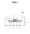
- a light-emitting device 100 has an LED substrate 1 whose cross-section is concave. On a concave portion (the bottom portion) of the LED substrate 1, a metal portion 2 is arranged. Above the metal portion 2, an LED element 3 in a rectangular shape is arranged. The LED element 3 is an example of a light-emitting element which emits light of a predetermined wavelength. On the surface of the LED element 3 facing to the metal portion 2, projecting electrodes 4 are arranged. The metal portion 2 and the LED element 3 are connected with each other through the projecting electrodes 4 (flip-chip type). Although illustrated here is the configuration such that one LED element 3 is arranged on one LED substrate 1, a plurality of the LED elements 3 can be arranged on the concave portion of one LED substrate 1.
- a blue LED element is used as the LED element 3.
- the blue LED element is, for example, constituted of a laminate of an n-GaN cladding layer, an InGaN fluorescent layer, a p-GaN cladding layer and a transparent electrode on a sapphire substrate.
- a wavelength conversion portion 6 is formed so as to seal a surrounding area of the LED element 3.
- the wavelength conversion portion 6 is a portion which converts light of a predetermined wavelength emitted from the LED element 3 to light of a wavelength different from the emitted light, and where a fluorescent substance which is excited with the wavelength from the LED element 3 and emits fluorescence of a wavelength different from the exciting wavelength is added in a translucent ceramic layer.
- the wavelength conversion portion 6 is formed so as to seal a surrounding area of the LED element 3 in this embodiment, the wavelength conversion portion 6 can be formed just around (on the upper and the side faces of) the LED element 3, and thus there can be a configuration such that the wavelength conversion portion 6 is not formed on the concave portion of the LED substrate 1.
- a method of forming the wavelength conversion portion 6 just around the LED element 3 an available method is, for example, placing a mask when the wavelength conversion portion 6 is formed.
- the wavelength conversion portion 6 is a clear ceramic layer (glass body) formed by turning a sol precursor solution where an organometallic compound is mixed with an organic solvent into a gel by heating followed by firing, which is called the sol-gel method.
- the clear ceramic layer includes the fluorescent substance, the layered silicate mineral, and inorganic fine particles.
- the organometallic compound functions as a binder for sealing the fluorescent substance, the layered silicate mineral, and the inorganic fine particles.
- organometallic compound used in the present invention such as a metal alkoxide, a metal acetylacetonate, a metal carboxylate can be given as the examples.
- a metal alkoxide which is easily turned into a gel by hydrolysis and polymerization, is suitable.
- a metal alcoxide can be monomolecular such as tetraethoxysilane, or can be a polysiloxane constituted of a chain or a ring of organosiloxane compounds.
- a polysiloxane which increases viscosity of the precursor solution is suitable.
- Types of metals of a metal alkoxide are not limited as long as a translucent glass body can be formed.
- silicon is included in a metal alkoxide.
- a plurality types of metals can be included therein.
- a content of the organometallic compound in the ceramic layer is less than 2% by weight, an amount of the organic compound as a binder is so low that strength of the ceramic layer after heated and fired decreases.
- the content of the organometallic compound in the ceramic layer is more than 50% by weight, contents of the layered silicate mineral and the inorganic fine particles are relatively low, and thus strength of the ceramic layer decreases. Therefore, the content of the organometallic compound in the ceramic layer ranges preferably from 2 to 50% by weight, and more preferably from 2.5 to 30% by weight.
- a polysilazane used in the present invention is represented by the following general formula (1): (R1R2SiNR3) n (1)
- R1, R2 and R3 independently represent hydrogen, an alkyl group, an aryl group, a vinyl group, or a cycloalkyl group. At least one of R1, R2 and R3 is hydrogen, and preferably all of R1, R2 and R3 are hydrogen, and "n" represents an integral number ranging from 1 to 60.
- a Polysilazane can be in any molecular shape, for example, can be a straight chain or a ring.
- a polysilazane represented by the above formula (1) and a reaction accelerating agent as needed are dissolved in an appropriate solvent, and application thereof is performed, and subsequently hardening is performed by heating, excimer light treatment, or UV light treatment.
- a ceramic layer having a high heat and light durability can be formed.
- hardening by irradiation of UVU radiation including light of wavelength of from 170 to 230nm (for example, excimer light) followed by heat hardening further enhances a water seepage-preventing effect.
- the reaction accelerating agent an acid or a base is suitably used.
- the reaction accelerating agent is not essential.
- the reaction accelerating agent such as triethylamine, diethylamine, N,N-dimethylethanolamine, triethanolamine, triethylamine, hydrochloric acid, oxalic acid, fumaric acid, sulfonic acid, acetic acid, and a metal carboxylate salt including a metal such as nickel, iron, palladium, iridium, platinum, titan, or aluminum can be given as the examples.
- the reaction accelerating agent is not limited to the above. If the reaction accelerating agent is used, a metal carboxylate salt is especially suitable. An amount thereof to be added ranges preferably from 0.01 to 5 mol% on the basis of a polysilazane.
- an aliphatic hydrocarbon an aromatic hydrocarbon, a halogen hydrocarbon, an ether, or an ester
- Methylethylketone, tetrahydrofuran, benzene, toluene, xylene, dimethylfluoride, chloroform, tetrachloromethane, ethylether, isopropylether, dibutylether, or ethylbutylether is suitable.
- a concentration of a polysilazane is preferably high.
- a polysilazane is dissolved in a solvent preferably from 5 to 50 wt% (% by weight). If a polysilazane solution is used as the ceramic precursor solution, in terms of suppressing deterioration of the glass material or the like used for a substrate, heating temperature in firing (firing temperature) ranges preferably from 150 to 500 °C, and more preferably from 150 to 350 °C.
- the fluorescent substance is excited with a wavelength of light emitted from the LED element 3 (an exciting wavelength), and emits fluorescence of a wavelength different from the exciting wavelength.
- an exciting wavelength a wavelength of light emitted from the LED element 3
- a YAG (yttrium ⁇ aluminum ⁇ garnet) fluorescent substance which converts blue light (of wavelengths from 420 to 485 nm) emitted from a blue LED element to yellow light (of wavelengths from 550 to 650 nm).
- oxides of Y, Gd, Ce, Sm, Al, La, or Ga, or compounds that are easily turned into oxides at a high temperature are used and mixed well in a stoichiometric ratio to obtain a raw mixture.
- a solution obtained by dissolving Y, Gd, Ce and Sm, which are rare earth elements, in an acid in a stoichiometric ratio is coprecipitated with oxalic acid, and fired to obtain coprecipitated oxide.
- the coprecipitated oxide is mixed with aluminum oxide and gallium oxide to obtain a raw mixture.
- a fluoride such as ammonium fluoride as a flux
- the obtained compact is put in a crucible, and fired at a temperature ranging from 1350 to 1450 °C for from 2 to 5 hours to obtain a sintered compact having a light-emitting characteristics of a fluorescent substance.
- a type of a fluorescent substance to be used is not limited thereto.
- other fluorescent substance such as a non-garnet fluorescent substance containing no Ce can be used.
- a larger particle diameter of a fluorescent substance provides a higher light-emitting efficiency (wavelength conversion efficiency), while providing bigger apertures formed around the interface between the organometallic compound and the fluorescent substance and a weaker layer strength of the ceramic layer.
- the average particle diameter of a fluorescent substance can be measured by, for example, the Coulter Counter Method.
- the layered silicate mineral is preferably a swelling clay mineral having the micaceous structure, the kaolinite structure, the smectite structure, or the like.
- the smectite structure which swells well, is especially suitable. This is because, as described below, water added to the fluorescent substance dispersion liquid enters into layer gaps of the smectite structure, and swells the structure to form a card house structure. Thus, even an added amount is small, viscosity of the fluorescent substance dispersion liquid can be much increased.
- the layered silicate mineral is in a plate-like structure in the ceramic layer, layer strength of the ceramic layer can be enhanced.
- the content of the layered silicate mineral in the ceramic layer is less than 0.5% by weight, an effect for increasing viscosity of the fluorescent substance dispersion liquid cannot be sufficiently obtained.
- the content of the layered silicate mineral is more than 20% by weight, strength of the ceramic layer decreases.
- the content of the layered silicate mineral ranges preferably from 0.5 to 20% by weight, and more preferably from 0.5 to 10% by weight.
- a layered silicate mineral whose surface is modified (a surface treatment) with an ammonium salt or the like can also be used as needed.
- the inorganic fine particles possess a filling effect for filling apertures therewith formed around the surfaces of the fluorescent substance and the layered silicate mineral; a viscosity-increasing effect for increasing viscosity of the fluorescent substance dispersion liquid; and a layer strength-enhancing effect for enhancing layer strength of the ceramic layer.
- oxide fine particles of such as a silicon oxide, a titanium oxide, zinc oxide, and fluoride fine particles of such as magnesium fluoride can be given as the examples.
- silicon oxide fine particles are suitably used.
- the content of the inorganic fine particles in the ceramic layer is set to be from 0.5 to 50% by weight.
- the content of the inorganic fine particles in the ceramic layer ranges from 0.5 to 40% by weight.
- an average particle diameter of the inorganic fine particles ranges preferably from 0.001 to 50 ⁇ m, and more preferably from 0.005 to 20 ⁇ m.
- the average particle diameter of the inorganic fine particles can be measured by, for example, the Coulter Counter Method.
- inorganic fine particles whose surfaces are modified with a silane coupling agent or a titanate coupling agent can also be used as needed.
- the precursor solution is a mixture of the organometallic compound with the organic solvent.
- the translucent ceramic layer can be obtained.
- the precursor solution is applied on the light-emitting element on which the fluorescent substance dispersion liquid where the fluorescent substance, the layered silicate mineral, and the inorganic fine particles are mixed has been applied, and subsequently heating is performed thereon, to form the wavelength conversion portion 6.
- the organic solvent an alcohol such as methanol, ethanol, propanol, butanol, or the like is suitable. If a mixture amount of the organometallic compound to the organic solvent is less than 5% by weight, it is difficult to increase viscosity of the precursor solution. If the mixture amount of the organometallic compound to the organic solvent is more than 50% by weight, polymerization reaction becomes too fast beyond necessity. Thus, the mixture amount of the organometallic compound to the organic solvent ranges preferably from 5 to 50% by weight, and more preferably from 8 to 40% by weight.
- the fluorescent substance dispersion liquid is a solution containing the fluorescent substance and the layered silicate mineral, and preferably, further containing the inorganic fine particles.
- a preparation protocol of the fluorescent substance dispersion liquid is, for example, if a lipophilic layered silicate mineral whose surface is treated is used, such that the layered silicate mineral is pre-mixed with the organic solvent first, and subsequently, the fluorescent substance, the inorganic fine particles, and water are mixed therewith.
- water is added to the fluorescent substance dispersion liquid, water enters into layer gaps of the layered silicate mineral, and thus viscosity of the fluorescent substance dispersion liquid increases. Accordingly, settlement of the fluorescent substance can be suppressed.
- an alcohol that has a high solubility in water such as methanol, ethanol, propanol, butanol, or the like is suitable.
- the layered silicate mineral is pre-mixed with water first, and subsequently, the fluorescent substance and the inorganic fine particles are mixed therewith.
- the layered silicate mineral can be evenly mixed, and the viscosity-increasing effect can be much enhanced.
- a preferred viscosity of the fluorescent substance dispersion liquid ranges from 25 to 800 cP, and the most preferred viscosity ranges from 30 to 500 cP. If water contains impurities, polymerization of the precursor solution may be suppressed. Thus, it is required that water to be added is purified water containing no impurities.
- a proportion of water to the total amount of the solvent is set be 5% or more by weight. If the proportion of water is less than 5% by weight, the viscosity-increasing effect mentioned above is not sufficiently obtained. If the proportion of water is more than 60% by weight, the viscosity-increasing effect is surpassed by a viscosity-decreasing effect resulted from addition of excess water.
- the proportion of water to the total solvent ranges preferably from 5 to 60% by weight, and more preferably from 7 to 55% by weight.
- a most preferred composition range of each of the above-mentioned materials in the fluorescent substance dispersion liquid is from 0.1 to 5% the layered silicate mineral and from 1 to 40% the inorganic fine particles by weight.
- the layered silicate mineral a layered silicate mineral having the smectite structure is suitably used.
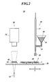
- a manufacturing device 10 of Fig. 2 is used to manufacture the wavelength conversion portion 6 of the light-emitting device 100.
- the manufacturing device 10 principally includes: a movable carriage 20 which can be moved upward, downward, leftward, rightward, forward and backward; a spraying unit 30 which can spray the above-described fluorescent substance dispersion liquid or the above-described precursor solution as an application liquid 40; and an inspecting unit 50 which can inspect such as chromaticity and brightness of the wavelength conversion portion 6.
- the spraying unit 30 is arranged above the movable carriage 20.
- the spraying unit 30 has a nozzle 32 to which air is supplied.
- the spraying unit 30 can be arranged below the movable carriage 20 and can spray the application liquid 40 upwards.
- a pore diameter of the tip of the nozzle 32 ranges from 20 ⁇ m to 2 mm, and preferably from 0.1 to 0.3 mm.
- the nozzle 32 can be moved upward, downward, leftward, rightward, forward and backward like the movable carriage 20. Particularly, an angle of the nozzle 32 can also be adjusted, and thus the nozzle 32 can be inclined with respect to the movable carriage 20 (or with respect to the LED substrate 1 to be put thereon).
- the nozzle 32 has a built-in temperature adjusting system, and thus temperatures of materials to be sprayed can be adjusted.
- the nozzle 32 is connected to a tank 36 through a connecting pipe 34.
- the tank 36 pools the application liquid 40.
- the tank 36 has a stirring bar therein, and the application liquid 40 is continuously stirred.
- the application liquid 40 is the fluorescent substance dispersion liquid
- the fluorescent substance having a high specific gravity may settle out of the fluorescent substance dispersion liquid, and thus concentration distribution of the fluorescent substance in the fluorescent substance dispersion liquid may become uneven.
- stirring the fluorescent substance dispersion liquid with the stirring bar in the tank 36 settlement of the fluorescent substance having a high specific gravity can be suppressed. Accordingly, the fluorescent substance can be kept in a dispersed state in the fluorescent substance dispersion liquid.
- the spraying unit 30 instead of supplying air to the nozzle 32, there is an adoptable mechanism such that pressure is supplied directly to the application liquid 40 in the tank 36 using such as a motor as a driver to spray the application liquid 40, or to push the application liquid 40 out from the nozzle 32.
- a motor as a driver to spray the application liquid 40
- unevenness of the pressure supplied to the application liquid 40 is set to be 10% or less.
- the inspecting unit 50 has an LED element 52 and a luminance colorimeter 54.
- the LED element 52 is an element which emits the same type of light as the LED element 3.
- the luminance colorimeter 54 is a measuring instrument for measuring chromaticity and brightness of received light.
- the fluorescent substance dispersion liquid is used as the application liquid 40 first, and sprayed to be applied in advance on a glass plate 60 for adjusting chromaticity and brightness (for a test use) to measure chromaticity and brightness of the white light beforehand (pre-spraying and applying step).
- the glass plate 60 is put on the movable carriage 20, and the movable carriage 20 and the nozzle 32 of the spraying unit 30 is adjusted such that the glass plate 60 and the tip of the nozzle 32 face each other. In this state, the fluorescent substance dispersion liquid is sprayed from the nozzle 32 and applied on the glass plate 60.
- the solvent in the fluorescent substance dispersion liquid volatilizes, and a fluorescent substance layer is formed on the glass plate 60.
- the glass plate 60 on which the fluorescent substance layer has been formed is moved near the inspecting unit 50, and the light-emitting element 52 is made emit light.
- chromaticity and brightness of the white light is measured with the luminance colorimeter 54 to inspect if chromaticity and brightness of the white light meet a desired value (a desired range).
- the process of the pre-spraying and applying step is repeated until chromaticity and brightness of the white light become stabilized.
- the chromaticity and brightness of the white light do not meet a desired value, such as spraying pressure and concentration of the fluorescent substance in the fluorescent substance dispersion liquid can be adjusted to make chromaticity and brightness of the white light meet a desired value.
- this adjustment is performed automatically according to the measured values.
- the adjustment can be performed manually according to the measured values.
- a plurality of the LED substrates 1 (on which the LED elements 3 have been disposed in advance) are put on the movable carriage 20, and a positional relationship between the LED substrate 1 and the nozzle 32 of the spraying unit 30 is adjusted (a position adjusting step).
- the LED substrates 1 are put on the movable carriage 20, and the LED substrate 1 and the tip of the nozzle 32 are positioned to face each other.
- the distance between the LED substrate 1 and the tip of the nozzle 32 is set to be from 5 to 30 cm.
- the tip of the nozzle 32 is apart from the LED substrate 1 at a fixed distance therebetween.
- the fluorescent substance dispersion liquid is sprayed from the nozzle 32 and applied on the LED substrate 1 (a spraying and applying step).
- the movable carriage 20 and the nozzle 32 are moved such that the LED substrate 1 and the nozzle 32 are moved forward, backward, leftward and rightward. Otherwise, either of the movable carriage 20 or the nozzle 32 can be fixed and the other can be moved forward, backward, leftward and rightward.
- the precursor solution is sprayed from the nozzle 32, and applied on the LED substrate 1 on which the fluorescent substance dispersion liquid has been applied.
- the LED substrate 1 on which the fluorescent substance dispersion liquid and the precursor solution have been applied is moved to a sintering furnace to be fired (a firing step).
- a treating temperature (a firing temperature) is set to a extent that the LED element 3 is not broken, ranging from 100 to 300 °C, preferably from 130 to 170 °C, more preferably from 140 to 160 °C, and most preferably around 150 °C.
- the precursor solution is sintered and the wavelength conversion portion 6 where the clear ceramic layer includes the fluorescent substance, the layered silicate mineral, and the inorganic fine particles is manufactured (formed).
- the top of the wavelength conversion portion 6 can be sealed with a silicone resin by using a dispenser. In this case, time-dependent deterioration of the wavelength conversion portion 6 can be suppressed, and adhesion properties of the wavelength conversion portion 6 to the LED substrate 1 and the LED element 3 can be enhanced.
- the fluorescent substance dispersion liquid containing the fluorescent substance is sprayed and applied on the LED element 3, and thereafter the precursor solution is applied on the LED element 3 on which the fluorescent substance dispersion liquid has been applied. Accordingly, the fluorescent substance can be applied on the LED element 3 in an evenly-dispersed state, and thus the wavelength conversion portion 6 where the fluorescent substance is evenly dispersed in the ceramic layer having a high heat durability can be formed.
- a second embodiment differs from the first embodiment in the following respects, and the other respects are the same as the first embodiment.
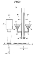
- a manufacturing device 70 of Fig. 3 instead of the manufacturing device 10 of Fig. 2 , a manufacturing device 70 of Fig. 3 is used.
- the manufacturing device 70 has a second spraying unit 80 in addition to the spraying unit 30.
- the spraying unit 80 has the same configuration as the spraying unit 30, and a tank 86 is connected to a nozzle 82 through a connecting pipe 84.
- the tank 36 of the spraying unit 30 pools the above-described precursor solution (42, the solution where the organometallic compound is mixed with the organic solvent).
- the tank 86 of the spraying unit 80 pools the above-described liquid where the fluorescent substance, the layered silicate mineral, and the inorganic fine particles are dispersed in the solvent (hereinafter referred to as a "fluorescent substance dispersion liquid 44").
- the materials of which the wavelength conversion portion 6 are composed are sprayed from the spraying unit 30 and the spraying unit 80 separately.
- the layered silicate mineral and the inorganic fine particles in the fluorescent substance dispersion liquid 44 can also be contained in the precursor solution 42.
- the fluorescent substance dispersion liquid 44 can be sprayed and applied in advance on the glass plate 60 for adjusting chromaticity and brightness (for a test use), to measure chromaticity and brightness of the white light beforehand.
- the nozzles 32 and 82 can be used (for spraying the precursor solution 42 and the fluorescent substance dispersion liquid 44) simultaneously or separately.
- the nozzles 32 and 82 are used simultaneously, if both the nozzles 32 and 82 are moved while their positional relationship is fixed, chromaticity of the wavelength conversion portion 6 can be stabilized.
- the fluorescent substance dispersion liquid 44 is sprayed from the nozzle 82 on each of the LED substrates 1 first, and thereafter the precursor solution 42 is sprayed from the nozzle 32 on the LED substrate 1.
- the precursor solution 42 can be sprayed right after the spraying of the fluorescent substance dispersion liquid 44, or can be sprayed at a predetermined time interval after the spraying of the fluorescent substance dispersion liquid 44. In the case of the spraying after a predetermined time interval, the solvent in the fluorescent substance dispersion liquid 44 can volatilize, and thus layer strength of the wavelength conversion portion 6 can be enhanced.
- the tips of the nozzle 32 and 82 are arranged right above the LED substrate 1, and each of the fluorescent substance dispersion liquid 44 and the precursor solution 42 is respectively sprayed from right above the LED element 3.
- the nozzle 82 is tilted to spray the fluorescent substance dispersion liquid 44 from the diagonal directions to the four corners of the LED element 3.
- fluorescent substance dispersion liquid 44 can also be applied evenly on the side faces of the LED element 3.
- the spraying angle can be set adequately as needed.
- the spraying angle is 45°.
- the nozzle 32 can be tilted to spray the precursor solution 42 from the diagonal directions to the four corners of the LED element 3.
- temperature adjustment is performed respectively on the nozzles 32 and 82 to adjust viscosities of the precursor solution 42 and the fluorescent substance dispersion liquid 44 to be the most preferred viscosities respectively.
- masks respectively exclusive to the precursor solution 42 and the fluorescent substance dispersion liquid 44 can be used, i.e., can be used according to materials to be sprayed. If the masks are used exclusively, the fluorescent substance, which is expensive, in the fluorescent substance dispersion liquid 44 can be collected and reused.
- the nozzle 82 can be cleaned.
- a cleaning tank which pools a cleaning solution is arranged near the spraying unit 80, and the tip of the nozzle 82 is dipped in the cleaning tank when, for example, the spraying of the application liquid 40 is stopped or chromaticity and brightness of the white light are being inspected, to prevent the tip portion of the nozzle 82 from being dried.
- the cleaning solution a solution capable of dissolving the fluorescent substance dispersion liquid 44 can be used.
- the fluorescent substance dispersion liquid 44 may harden to plug an spraying exit of the nozzle 82.
- the nozzle 82 it is preferable to dip the nozzle 82 in the cleaning tank, or to clean the nozzle 82 at the start of the spraying and applying step.
- the cleaning of the nozzle 82 can be performed before performance of the spraying and applying step itself.
- the nozzle 32 can be cleaned in the same manner as the cleaning of the nozzle 82 before or during the spraying and applying step.
- the LED substrate 1 on which both the fluorescent substance dispersion liquid 44 and the precursor solution 42 have been sequentially applied can be heated and fired. Otherwise, the LED substrate 1 on which the fluorescent substance dispersion liquid 44 has been applied can be heated first to volatilize the solvent and form the fluorescent substance layer, and subsequently the precursor solution 42 can be applied on the LED substrate 1 followed by heating and firing. Also when the fluorescent substance dispersion liquid 44 and the precursor solution 42 are heated and fired simultaneously, treating temperature (firing temperature) is set to an extent that the LED element 3 is not broken, ranging from 100 to 300 °C, preferably from 130 to 170 °C, more preferably from 140 to 160 °C, and most preferably about 150 °C.
- each treating temperature is set to an extent that the LED element 3 is not broken, ranging from 100 to 300 °C, preferably from 130 to 170 °C, more preferably from 140 to 160 °C, and most preferably about 150 °C.
- the precursor solution 42 and the fluorescent substance dispersion liquid 44 are sprayed and applied on the LED element 3 separately.
- spraying volume, spraying pressure, viscosity of each of the liquid and the solution can be optimized more adequately, and the fluorescent substance can be applied evenly on the LED element 3 in a more dispersed state.
- the use of one nozzle 32 and the use of two nozzles 32 and 82 are exemplary described.
- the number of the nozzles can be three or more (can be modified) according to types of materials to be sprayed.
- three spraying units which are the same as the spraying unit 30 can be used to spray solutions each of which contains each fluorescent substance from three nozzles separately.
- Y 2 O 3 (7.41 g), Gd 2 O 3 (4.01 g), CeO 2 (0.63 g), and Al 2 O 3 (7.77 g) were well mixed, and an adequate amount of ammonium fluoride as a flux was added therewith. Then, this mixture was put in an aluminum crucible and fired under a reducing atmosphere by ventilating nitrogen gas with hydrogen gas at a temperature ranging from 1350 to 1450 °C for from 2 to 5 hours to obtain a fired product ((Y 0.72 Gd 0.24 ) 3 Al 5 O 12 :Ce 0.04 ).
- the obtained fired product was milled, washed, separated, and dried to obtain yellow fluorescent substance particles having a volume-mean particle diameter of about 1 ⁇ m. Thereafter, an emission wavelength of an excitation light of the fluorescent substance particles at a wavelength of 465 nm was measured, and a peak wavelength was at about 570 nm (a glass substrate).
- a fluorescent substance dispersion liquid 0.11 g of hydrophilic smectite whose surface was not treated (Lucentite SWN, Co-op Chemical Co. , Ltd.) was mixed with and dispersed in 2.2 g of purified water. Then, 1 g of the above prepared fluorescent substance and 4.4 g of IPA were further mixed therewith to prepare a fluorescent substance dispersion liquid. This fluorescent substance dispersion liquid was sprayed by the spray coating method on the concave portion of the LED substrate (the substrate on which 20 blue LED chips have been disposed in advance) and the surfaces of the LED chips so as to form a fluorescent substance layer having a layer thickness of 35 ⁇ m after heated. Then heating was performed thereon at 50 °C for 10 minutes to form a fluorescent substance layer.
- a precursor solution ( NL120-20 ; 20% polysilazane and 80% dibuthylether by weight; AZ Electronic Materials) was sprayed by the spray coating method on the fluorescent substance layer.
- the fluorescent substance layer was impregnated with the precursor solution, and the precursor solution filled apertures formed around the surfaces of the fluorescent substance and the hydrophilic smectite, which are compositions of the fluorescent substance layer.
- heating is performed thereon at 150 °C for 1 hour to form a wavelength conversion portion.
- a light-emitting device manufactured by these processes was named "Sample (Example 2)".
- 0.05 g of hydrophilic smectite whose surface was not treated (Lucentite SWN, Co-op Chemical Co., Ltd.), 0.05 g of inorganic particles (RX300, Nippon Aerosil Co., Ltd., particle diameter of 7 nm), and 0.75 g of the prepared fluorescent substance were mixed with 0.5 g of water, and further 1 g of isopropyl alcohol (IPA) were mixed therewith, to prepare a fluorescent substance dispersion liquid.
- IPA isopropyl alcohol
- This fluorescent substance dispersion liquid was sprayed by the spray coating method on the concave portion of the LED substrate (the substrate on which 20 blue LED chips have been disposed in advance) and the surfaces of the LED chips so as to form a fluorescent substance layer having a layer thickness of 55 ⁇ m after heated. Then heating was performed thereon at 50 °C for 1 hour to form a fluorescent substance layer. Thereafter, a precursor solution (14% polysiloxane and 86% isopropyl alcohol by weight) was sprayed by the spray coating method on the fluorescent substance layer.
- the fluorescent substance layer was impregnated with the precursor solution, and the precursor solution filled apertures formed around the surfaces of the fluorescent substance, the hydrophilic smectite and the inorganic particles, which are compositions of the fluorescent substance layer. Then heating is performed thereon at 150 °C for 1 hour to form a wavelength conversion portion.
- a light-emitting device manufactured by these processes was named "Sample (Example 3)".
- a fluorescent substance dispersion liquid 0. 04 g of synthetic mica (MICROMICA MK-100, Co-op Chemical Co., Ltd.) and 0.81 g of the above fluorescent substance were mixed with 1 g of propylene glycol to prepare a fluorescent substance dispersion liquid.
- This fluorescent substance dispersion liquid was sprayed by the spray coating method on the concave portion of the LED substrate (the substrate on which 20 blue LED chips have been disposed in advance) and the surfaces of the LED chips so as to form a fluorescent substance layer having a layer thickness of 50 ⁇ m after heated. Then drying was performed thereon at 50 °C for 1 hour to form a fluorescent substance layer.
- a precursor solution (14% polysiloxane and 86% IPA by weight) was sprayed by the spray coating method on the fluorescent substance layer.
- the fluorescent substance layer was impregnated with the precursor solution, and the precursor solution filled apertures formed around the surfaces of the fluorescent substance and the synthetic mica, which are compositions of the fluorescent substance layer.
- heating is performed thereon at 150 °C for 1 hour to form a wavelength conversion portion.
- a light-emitting device manufactured by these processes was named "Sample (Example 4)".
- fluorescent substance dispersion liquid 0.065 g of inorganic particles (RX300, Nippon Aerosil Co., Ltd., particle diameter of 7 nm), 0.025 g of hydrophilic smectite (Lucentite SWN, Co-op Chemical Co. , Ltd.), and 1 g of the fluorescent substance were mixed with 1 g of 1,3-butanediol and 0.75 g of isopropyl alcohol to prepare a fluorescent substance dispersion liquid.
- This fluorescent substance dispersion liquid was sprayed by the spray coating method on the concave portion of the LED substrate (the substrate on which 20 blue LED chips have been disposed in advance) and the surfaces of the LED chips so as to form a fluorescent substance layer having a layer thickness of 45 ⁇ m after heated.
- 0.3 g of the above prepared fluorescent substance was mixed with 1 g of a polysiloxane dispersion liquid (14% polysiloxane and 86% isopropyl alcohol by weight) to prepare a application liquid for forming a wavelength conversion portion.
- This application liquid for forming a wavelength conversion portion was sprayed and applied on the concave portion of the LED substrate (the substrate on which 20 blue LED chips have been disposed in advance) and the surfaces of the LED chips so as to form a fluorescent substance layer having a layer thickness of 45 ⁇ m after heated. Then heating was performed thereon at 150 °C for 1 hour to form a wavelength conversion portion.
- a light-emitting device manufactured by these processes was named "Sample (Comparative Example 1)".
- Layer thicknesses of each of the Samples were measured with a laser hologage (Mitutoyo Corporation), and a variation of the layer thicknesses was evaluated. An evaluation result is shown in Table 1. Regarding the evaluation of the layer thickness shown in Table 1, an average of layer thicknesses on the LED chips of one sample piece on which the applying was firstly performed among the five sample pieces of the Sample was determined as a standard thickness (100%).
- viscosities of the fluorescent substance dispersion liquids are also shown.
- the viscosities of the fluorescent substance dispersion liquids and the application liquid for forming the wavelength conversion portion were measured with a vibrational viscometer (VM-10A-L, CBC Co.,Ltd.).
- the LED chips of the Samples were made emit light, and chromaticity of the emitted light was measured with a spectroradiometer (CS-1000A, Konica Minolta Sensing Inc.). A measurement result is shown in Table 1.
- Chromaticity of white light is (0.33, 0.33). When chromaticity of light is closer to these values, the light is closer to white light. When a value of the X coordinate is small, a color of the light is bluish white. When a value of the X coordinate is large, a color of the light is yellowish white.
- Each of five chromaticities in Table 2 represents chromaticity of the respective five sample pieces.
- the each value of the sample piece is an average of three chromaticities obtained by measuring lights emitted from three LED chips which were arbitrarily selected among the plurality of LED chips on each of the LED substrate.
- the present invention is suitably applicable to a method of manufacturing a light-emitting device for dispersing a fluorescent substance evenly in a translucent material having a high heat durability.
Landscapes
- Engineering & Computer Science (AREA)
- Manufacturing & Machinery (AREA)
- Computer Hardware Design (AREA)
- Microelectronics & Electronic Packaging (AREA)
- Power Engineering (AREA)
- Led Device Packages (AREA)
- Application Of Or Painting With Fluid Materials (AREA)
Applications Claiming Priority (2)
| Application Number | Priority Date | Filing Date | Title |
|---|---|---|---|
| JP2010182211 | 2010-08-17 | ||
| PCT/JP2011/067635 WO2012023425A1 (ja) | 2010-08-17 | 2011-08-02 | 発光装置の製造方法 |
Publications (1)
| Publication Number | Publication Date |
|---|---|
| EP2608284A1 true EP2608284A1 (en) | 2013-06-26 |
Family
ID=45605081
Family Applications (1)
| Application Number | Title | Priority Date | Filing Date |
|---|---|---|---|
| EP11818067.8A Withdrawn EP2608284A1 (en) | 2010-08-17 | 2011-08-02 | Method of manufacturing light-emitting device |
Country Status (6)
| Country | Link |
|---|---|
| US (3) | US8835192B2 (enExample) |
| EP (1) | EP2608284A1 (enExample) |
| JP (3) | JP5299577B2 (enExample) |
| KR (1) | KR101478472B1 (enExample) |
| CN (2) | CN103081142B (enExample) |
| WO (2) | WO2012023425A1 (enExample) |
Cited By (3)
| Publication number | Priority date | Publication date | Assignee | Title |
|---|---|---|---|---|
| DE102012112316A1 (de) * | 2012-12-14 | 2014-06-18 | Osram Opto Semiconductors Gmbh | Verfahren und Vorrichtung zur Herstellung eines Strahlung emittierenden Halbleiterbauelements und Strahlung emittierendes Halbleiterbauelement |
| EP2685512A4 (en) * | 2011-03-11 | 2014-09-03 | Konica Minolta Inc | METHOD FOR PRODUCING A LIGHT-EMITTING DEVICE AND A MIXING PHOSPHORIZED SOLUTION |
| EP2752897A4 (en) * | 2011-10-07 | 2015-04-29 | Konica Minolta Inc | MANUFACTURING METHOD FÜRLED DEVICE AND FLUORESCENT FABRICED DISPERSED SOLUTION USING THEREOF |
Families Citing this family (18)
| Publication number | Priority date | Publication date | Assignee | Title |
|---|---|---|---|---|
| JP5310700B2 (ja) * | 2010-10-27 | 2013-10-09 | パナソニック株式会社 | Ledパッケージ製造システムおよびledパッケージ製造システムにおける樹脂塗布方法 |
| JP5310699B2 (ja) * | 2010-10-27 | 2013-10-09 | パナソニック株式会社 | 樹脂塗布装置および樹脂塗布方法 |
| JP5413404B2 (ja) | 2011-05-30 | 2014-02-12 | パナソニック株式会社 | Ledパッケージ製造システムおよびledパッケージ製造システムにおける樹脂塗布方法 |
| JP5413405B2 (ja) * | 2011-05-30 | 2014-02-12 | パナソニック株式会社 | 樹脂塗布装置および樹脂塗布方法 |
| WO2013121646A1 (ja) * | 2012-02-16 | 2013-08-22 | コニカミノルタ株式会社 | 発光装置の製造方法及び蛍光体塗布装置 |
| JP2013258339A (ja) * | 2012-06-13 | 2013-12-26 | Konica Minolta Inc | 発光装置及びその製造方法 |
| EP2853577A4 (en) | 2012-08-13 | 2016-01-06 | Konica Minolta Inc | METHOD FOR PRODUCING A PHOSPHORDISPERSION LIQUID AND METHOD FOR PRODUCING AN LED DEVICE |
| JP5994628B2 (ja) * | 2012-12-26 | 2016-09-21 | 日亜化学工業株式会社 | 発光装置の製造方法およびスプレーコーティング装置 |
| EP2940744A4 (en) * | 2012-12-27 | 2016-06-29 | Konica Minolta Inc | PHOSPHORDISPERSION, LED DEVICE AND METHOD FOR THE PRODUCTION THEREOF |
| WO2014199926A1 (ja) * | 2013-06-13 | 2014-12-18 | 旭硝子株式会社 | 蛍光体分散シートの色度座標検査方法、蛍光体分散シートの製造方法、光変換部材の製造方法およびledパッケージの製造方法 |
| KR101474376B1 (ko) * | 2013-11-28 | 2014-12-18 | 주식회사 말콤 | 온도표시기능을 구비하는 led패키지용 시린지 및 이를 이용하는 led패키지 제조방법 |
| CN103840068B (zh) * | 2013-12-31 | 2017-09-19 | 杨毅 | 波长转换装置和发光装置 |
| TWI575778B (zh) * | 2014-05-07 | 2017-03-21 | 新世紀光電股份有限公司 | 發光二極體封裝結構 |
| KR102237112B1 (ko) | 2014-07-30 | 2021-04-08 | 엘지이노텍 주식회사 | 발광 소자 및 이를 구비한 광원 모듈 |
| KR20180011398A (ko) | 2016-07-21 | 2018-02-01 | 삼성디스플레이 주식회사 | 표시 장치 및 이의 제조 방법 |
| CN107611241A (zh) * | 2017-10-23 | 2018-01-19 | 苏州创思得新材料有限公司 | 一种多相复合的Re,Ce:YAG陶瓷荧光片及其制备方法 |
| KR102053614B1 (ko) * | 2018-06-19 | 2019-12-09 | 주식회사 네모엘텍 | 퀀텀닷 led 조명 및 제조 장치 |
| CN108962798B (zh) * | 2018-08-03 | 2024-07-05 | 华南理工大学 | 三基色rgb-led全自动荧光粉胶高速智能涂覆设备及方法 |
Family Cites Families (17)
| Publication number | Priority date | Publication date | Assignee | Title |
|---|---|---|---|---|
| JPH11106685A (ja) * | 1997-10-02 | 1999-04-20 | Nemoto Tokushu Kagaku Kk | 蓄光性塗料及びこの塗料を用いた表示体 |
| JP3307316B2 (ja) * | 1998-02-27 | 2002-07-24 | サンケン電気株式会社 | 半導体発光装置 |
| JP2001181614A (ja) * | 1999-12-24 | 2001-07-03 | Teikoku Tsushin Kogyo Co Ltd | El素子用蛍光体ペースト及びその製造方法 |
| JP3614776B2 (ja) | 2000-12-19 | 2005-01-26 | シャープ株式会社 | チップ部品型ledとその製造方法 |
| JP4101468B2 (ja) | 2001-04-09 | 2008-06-18 | 豊田合成株式会社 | 発光装置の製造方法 |
| CN1323441C (zh) * | 2001-10-12 | 2007-06-27 | 日亚化学工业株式会社 | 发光装置及其制造方法 |
| JP4306224B2 (ja) * | 2002-10-31 | 2009-07-29 | パナソニック電工株式会社 | 発光装置の製造方法 |
| US6789874B1 (en) | 2003-02-28 | 2004-09-14 | Eastman Kodak Company | Method of cleaning nozzles in inkjet printhead |
| JP2005064233A (ja) * | 2003-08-12 | 2005-03-10 | Stanley Electric Co Ltd | 波長変換型led |
| JP4451178B2 (ja) | 2004-03-25 | 2010-04-14 | スタンレー電気株式会社 | 発光デバイス |
| JP2007123417A (ja) * | 2005-10-26 | 2007-05-17 | Toyoda Gosei Co Ltd | 発光装置の製造方法 |
| JP5167582B2 (ja) | 2005-10-28 | 2013-03-21 | 住友大阪セメント株式会社 | ジルコニア透明分散液及び透明複合体並びに透明複合体の製造方法 |
| KR100862532B1 (ko) * | 2007-03-13 | 2008-10-09 | 삼성전기주식회사 | 발광 다이오드 패키지 제조방법 |
| KR101408450B1 (ko) | 2007-03-28 | 2014-06-17 | 가부시키가이샤 구라레 | M-c-n-o계 형광체 |
| JP5552748B2 (ja) * | 2008-03-28 | 2014-07-16 | 三菱化学株式会社 | 硬化性ポリシロキサン組成物、並びに、それを用いたポリシロキサン硬化物、光学部材、航空宇宙産業用部材、半導体発光装置、照明装置、及び画像表示装置 |
| JP5380027B2 (ja) | 2008-09-25 | 2014-01-08 | 株式会社フジクラ | 発光装置の製造方法 |
| CN101494271A (zh) * | 2009-02-20 | 2009-07-29 | 隆达电子股份有限公司 | 发光二极管装置的制造方法及喷涂设备 |
-
2011
- 2011-08-02 KR KR1020137003657A patent/KR101478472B1/ko not_active Expired - Fee Related
- 2011-08-02 WO PCT/JP2011/067635 patent/WO2012023425A1/ja not_active Ceased
- 2011-08-02 US US13/817,371 patent/US8835192B2/en not_active Expired - Fee Related
- 2011-08-02 CN CN201180040060.0A patent/CN103081142B/zh not_active Expired - Fee Related
- 2011-08-02 US US13/817,320 patent/US9153752B2/en active Active
- 2011-08-02 JP JP2012529552A patent/JP5299577B2/ja not_active Expired - Fee Related
- 2011-08-02 EP EP11818067.8A patent/EP2608284A1/en not_active Withdrawn
- 2011-08-02 CN CN201410769338.3A patent/CN104576899A/zh active Pending
- 2011-08-02 WO PCT/JP2011/067634 patent/WO2012023424A1/ja not_active Ceased
- 2011-08-02 JP JP2012529551A patent/JP5870923B2/ja not_active Expired - Fee Related
-
2013
- 2013-06-20 JP JP2013129097A patent/JP5900425B2/ja not_active Expired - Fee Related
-
2014
- 2014-08-07 US US14/454,108 patent/US9306130B2/en active Active
Non-Patent Citations (1)
| Title |
|---|
| See references of WO2012023425A1 * |
Cited By (5)
| Publication number | Priority date | Publication date | Assignee | Title |
|---|---|---|---|---|
| EP2685512A4 (en) * | 2011-03-11 | 2014-09-03 | Konica Minolta Inc | METHOD FOR PRODUCING A LIGHT-EMITTING DEVICE AND A MIXING PHOSPHORIZED SOLUTION |
| EP2752897A4 (en) * | 2011-10-07 | 2015-04-29 | Konica Minolta Inc | MANUFACTURING METHOD FÜRLED DEVICE AND FLUORESCENT FABRICED DISPERSED SOLUTION USING THEREOF |
| US9318646B2 (en) | 2011-10-07 | 2016-04-19 | Konica Minolta, Inc. | LED device manufacturing method and fluorescent material-dispersed solution used in same |
| DE102012112316A1 (de) * | 2012-12-14 | 2014-06-18 | Osram Opto Semiconductors Gmbh | Verfahren und Vorrichtung zur Herstellung eines Strahlung emittierenden Halbleiterbauelements und Strahlung emittierendes Halbleiterbauelement |
| WO2014091003A1 (de) * | 2012-12-14 | 2014-06-19 | Osram Opto Semiconductors Gmbh | Verfahren und vorrichtung zur herstellung einer leuchtdiode |
Also Published As
| Publication number | Publication date |
|---|---|
| JP5870923B2 (ja) | 2016-03-01 |
| CN103081142A (zh) | 2013-05-01 |
| JP2013229621A (ja) | 2013-11-07 |
| KR101478472B1 (ko) | 2014-12-31 |
| WO2012023424A1 (ja) | 2012-02-23 |
| JPWO2012023425A1 (ja) | 2013-10-28 |
| KR20130028148A (ko) | 2013-03-18 |
| US8835192B2 (en) | 2014-09-16 |
| CN103081142B (zh) | 2015-01-14 |
| US20130149801A1 (en) | 2013-06-13 |
| US9153752B2 (en) | 2015-10-06 |
| US20130143343A1 (en) | 2013-06-06 |
| WO2012023425A1 (ja) | 2012-02-23 |
| JPWO2012023424A1 (ja) | 2013-10-28 |
| US9306130B2 (en) | 2016-04-05 |
| JP5900425B2 (ja) | 2016-04-06 |
| CN104576899A (zh) | 2015-04-29 |
| JP5299577B2 (ja) | 2013-09-25 |
| US20140349419A1 (en) | 2014-11-27 |
Similar Documents
| Publication | Publication Date | Title |
|---|---|---|
| US9306130B2 (en) | Method of manufacturing light-emitting device | |
| EP2752897A1 (en) | Led device manufacturing method and fluorescent material-dispersed solution used in same | |
| JP5869769B2 (ja) | 蛍光体層の形成方法および発光装置の製造方法 | |
| EP2685512A1 (en) | Method for manufacturing light emitting device and mixed phosphor solution | |
| JPWO2012086483A1 (ja) | 蛍光体塗布装置および発光装置の製造方法 | |
| JP5510312B2 (ja) | 発光装置の製造方法 | |
| EP2763197A1 (en) | Phosphor dispersion liquid and method for manufacturing led device | |
| JP5803541B2 (ja) | Led装置およびその製造方法、並びにそれに用いる蛍光体分散液 | |
| WO2013121903A1 (ja) | 波長変換素子及びその製造方法、発光装置及びその製造方法 | |
| JP5880566B2 (ja) | Led装置 | |
| JP5729327B2 (ja) | Led装置の製造方法 | |
| WO2012090966A1 (ja) | 発光装置およびその製造方法 | |
| JP5765428B2 (ja) | Led装置の製造方法 | |
| JP5870736B2 (ja) | 蛍光体分散液の製造方法、およびそれを用いてled装置を製造する方法 | |
| JP5617737B2 (ja) | 発光装置の製造方法、発光装置及び蛍光体粒子分散液 | |
| JP2012195522A (ja) | 発光装置の製造方法 |
Legal Events
| Date | Code | Title | Description |
|---|---|---|---|
| PUAI | Public reference made under article 153(3) epc to a published international application that has entered the european phase |
Free format text: ORIGINAL CODE: 0009012 |
|
| 17P | Request for examination filed |
Effective date: 20130214 |
|
| AK | Designated contracting states |
Kind code of ref document: A1 Designated state(s): AL AT BE BG CH CY CZ DE DK EE ES FI FR GB GR HR HU IE IS IT LI LT LU LV MC MK MT NL NO PL PT RO RS SE SI SK SM TR |
|
| DAX | Request for extension of the european patent (deleted) | ||
| STAA | Information on the status of an ep patent application or granted ep patent |
Free format text: STATUS: THE APPLICATION HAS BEEN WITHDRAWN |
|
| 18W | Application withdrawn |
Effective date: 20160321 |