US6800508B2 - Semiconductor device, its manufacturing method and electrodeposition frame - Google Patents
Semiconductor device, its manufacturing method and electrodeposition frame Download PDFInfo
- Publication number
- US6800508B2 US6800508B2 US09/837,022 US83702201A US6800508B2 US 6800508 B2 US6800508 B2 US 6800508B2 US 83702201 A US83702201 A US 83702201A US 6800508 B2 US6800508 B2 US 6800508B2
- Authority
- US
- United States
- Prior art keywords
- metallic
- semiconductor device
- metallic layers
- resin
- semiconductor
- Prior art date
- Legal status (The legal status is an assumption and is not a legal conclusion. Google has not performed a legal analysis and makes no representation as to the accuracy of the status listed.)
- Expired - Lifetime
Links
- 239000004065 semiconductor Substances 0.000 title claims abstract description 150
- 238000004070 electrodeposition Methods 0.000 title claims description 28
- 238000004519 manufacturing process Methods 0.000 title claims description 22
- 229920005989 resin Polymers 0.000 claims abstract description 67
- 239000011347 resin Substances 0.000 claims abstract description 67
- 238000007789 sealing Methods 0.000 claims abstract description 38
- 239000000758 substrate Substances 0.000 claims description 69
- 239000010409 thin film Substances 0.000 claims description 28
- 238000005520 cutting process Methods 0.000 claims description 10
- 238000000151 deposition Methods 0.000 claims description 5
- QXZUUHYBWMWJHK-UHFFFAOYSA-N [Co].[Ni] Chemical compound [Co].[Ni] QXZUUHYBWMWJHK-UHFFFAOYSA-N 0.000 description 25
- PXHVJJICTQNCMI-UHFFFAOYSA-N nickel Substances [Ni] PXHVJJICTQNCMI-UHFFFAOYSA-N 0.000 description 20
- 229910052759 nickel Inorganic materials 0.000 description 18
- 239000010931 gold Substances 0.000 description 15
- 239000010408 film Substances 0.000 description 14
- 229910045601 alloy Inorganic materials 0.000 description 13
- 239000000956 alloy Substances 0.000 description 13
- 229910052737 gold Inorganic materials 0.000 description 12
- 239000011521 glass Substances 0.000 description 11
- PCHJSUWPFVWCPO-UHFFFAOYSA-N gold Chemical compound [Au] PCHJSUWPFVWCPO-UHFFFAOYSA-N 0.000 description 11
- 239000004593 Epoxy Substances 0.000 description 10
- 238000000034 method Methods 0.000 description 9
- 238000000465 moulding Methods 0.000 description 6
- 239000010935 stainless steel Substances 0.000 description 5
- 229910001220 stainless steel Inorganic materials 0.000 description 5
- 239000003822 epoxy resin Substances 0.000 description 4
- 229920000647 polyepoxide Polymers 0.000 description 4
- 229910001020 Au alloy Inorganic materials 0.000 description 3
- 239000000919 ceramic Substances 0.000 description 3
- 230000017525 heat dissipation Effects 0.000 description 3
- 229910052709 silver Inorganic materials 0.000 description 3
- 229910000531 Co alloy Inorganic materials 0.000 description 2
- RYGMFSIKBFXOCR-UHFFFAOYSA-N Copper Chemical compound [Cu] RYGMFSIKBFXOCR-UHFFFAOYSA-N 0.000 description 2
- 229910052802 copper Inorganic materials 0.000 description 2
- 239000010949 copper Substances 0.000 description 2
- 238000009713 electroplating Methods 0.000 description 2
- 238000005530 etching Methods 0.000 description 2
- 239000003353 gold alloy Substances 0.000 description 2
- 229910000990 Ni alloy Inorganic materials 0.000 description 1
- BQCADISMDOOEFD-UHFFFAOYSA-N Silver Chemical compound [Ag] BQCADISMDOOEFD-UHFFFAOYSA-N 0.000 description 1
- 239000000853 adhesive Substances 0.000 description 1
- 230000001070 adhesive effect Effects 0.000 description 1
- 239000002659 electrodeposit Substances 0.000 description 1
- 239000011159 matrix material Substances 0.000 description 1
- 239000004332 silver Substances 0.000 description 1
- 238000004528 spin coating Methods 0.000 description 1
- 238000004544 sputter deposition Methods 0.000 description 1
- 230000035882 stress Effects 0.000 description 1
- 230000008646 thermal stress Effects 0.000 description 1
- 238000001771 vacuum deposition Methods 0.000 description 1
Images


Classifications
-
- H—ELECTRICITY
- H01—ELECTRIC ELEMENTS
- H01L—SEMICONDUCTOR DEVICES NOT COVERED BY CLASS H10
- H01L21/00—Processes or apparatus adapted for the manufacture or treatment of semiconductor or solid state devices or of parts thereof
- H01L21/02—Manufacture or treatment of semiconductor devices or of parts thereof
- H01L21/04—Manufacture or treatment of semiconductor devices or of parts thereof the devices having at least one potential-jump barrier or surface barrier, e.g. PN junction, depletion layer or carrier concentration layer
- H01L21/50—Assembly of semiconductor devices using processes or apparatus not provided for in a single one of the subgroups H01L21/06 - H01L21/326, e.g. sealing of a cap to a base of a container
- H01L21/56—Encapsulations, e.g. encapsulation layers, coatings
- H01L21/568—Temporary substrate used as encapsulation process aid
-
- H—ELECTRICITY
- H01—ELECTRIC ELEMENTS
- H01L—SEMICONDUCTOR DEVICES NOT COVERED BY CLASS H10
- H01L21/00—Processes or apparatus adapted for the manufacture or treatment of semiconductor or solid state devices or of parts thereof
- H01L21/02—Manufacture or treatment of semiconductor devices or of parts thereof
- H01L21/04—Manufacture or treatment of semiconductor devices or of parts thereof the devices having at least one potential-jump barrier or surface barrier, e.g. PN junction, depletion layer or carrier concentration layer
- H01L21/50—Assembly of semiconductor devices using processes or apparatus not provided for in a single one of the subgroups H01L21/06 - H01L21/326, e.g. sealing of a cap to a base of a container
- H01L21/56—Encapsulations, e.g. encapsulation layers, coatings
- H01L21/561—Batch processing
-
- H—ELECTRICITY
- H01—ELECTRIC ELEMENTS
- H01L—SEMICONDUCTOR DEVICES NOT COVERED BY CLASS H10
- H01L23/00—Details of semiconductor or other solid state devices
- H01L23/28—Encapsulations, e.g. encapsulating layers, coatings, e.g. for protection
- H01L23/31—Encapsulations, e.g. encapsulating layers, coatings, e.g. for protection characterised by the arrangement or shape
- H01L23/3107—Encapsulations, e.g. encapsulating layers, coatings, e.g. for protection characterised by the arrangement or shape the device being completely enclosed
-
- H—ELECTRICITY
- H01—ELECTRIC ELEMENTS
- H01L—SEMICONDUCTOR DEVICES NOT COVERED BY CLASS H10
- H01L24/00—Arrangements for connecting or disconnecting semiconductor or solid-state bodies; Methods or apparatus related thereto
- H01L24/93—Batch processes
- H01L24/95—Batch processes at chip-level, i.e. with connecting carried out on a plurality of singulated devices, i.e. on diced chips
- H01L24/97—Batch processes at chip-level, i.e. with connecting carried out on a plurality of singulated devices, i.e. on diced chips the devices being connected to a common substrate, e.g. interposer, said common substrate being separable into individual assemblies after connecting
-
- H—ELECTRICITY
- H01—ELECTRIC ELEMENTS
- H01L—SEMICONDUCTOR DEVICES NOT COVERED BY CLASS H10
- H01L2224/00—Indexing scheme for arrangements for connecting or disconnecting semiconductor or solid-state bodies and methods related thereto as covered by H01L24/00
- H01L2224/01—Means for bonding being attached to, or being formed on, the surface to be connected, e.g. chip-to-package, die-attach, "first-level" interconnects; Manufacturing methods related thereto
- H01L2224/02—Bonding areas; Manufacturing methods related thereto
- H01L2224/04—Structure, shape, material or disposition of the bonding areas prior to the connecting process
- H01L2224/05—Structure, shape, material or disposition of the bonding areas prior to the connecting process of an individual bonding area
- H01L2224/0554—External layer
- H01L2224/0555—Shape
- H01L2224/05552—Shape in top view
- H01L2224/05553—Shape in top view being rectangular
-
- H—ELECTRICITY
- H01—ELECTRIC ELEMENTS
- H01L—SEMICONDUCTOR DEVICES NOT COVERED BY CLASS H10
- H01L2224/00—Indexing scheme for arrangements for connecting or disconnecting semiconductor or solid-state bodies and methods related thereto as covered by H01L24/00
- H01L2224/01—Means for bonding being attached to, or being formed on, the surface to be connected, e.g. chip-to-package, die-attach, "first-level" interconnects; Manufacturing methods related thereto
- H01L2224/42—Wire connectors; Manufacturing methods related thereto
- H01L2224/44—Structure, shape, material or disposition of the wire connectors prior to the connecting process
- H01L2224/45—Structure, shape, material or disposition of the wire connectors prior to the connecting process of an individual wire connector
- H01L2224/45001—Core members of the connector
- H01L2224/45099—Material
- H01L2224/451—Material with a principal constituent of the material being a metal or a metalloid, e.g. boron (B), silicon (Si), germanium (Ge), arsenic (As), antimony (Sb), tellurium (Te) and polonium (Po), and alloys thereof
- H01L2224/45138—Material with a principal constituent of the material being a metal or a metalloid, e.g. boron (B), silicon (Si), germanium (Ge), arsenic (As), antimony (Sb), tellurium (Te) and polonium (Po), and alloys thereof the principal constituent melting at a temperature of greater than or equal to 950°C and less than 1550°C
- H01L2224/45144—Gold (Au) as principal constituent
-
- H—ELECTRICITY
- H01—ELECTRIC ELEMENTS
- H01L—SEMICONDUCTOR DEVICES NOT COVERED BY CLASS H10
- H01L2224/00—Indexing scheme for arrangements for connecting or disconnecting semiconductor or solid-state bodies and methods related thereto as covered by H01L24/00
- H01L2224/01—Means for bonding being attached to, or being formed on, the surface to be connected, e.g. chip-to-package, die-attach, "first-level" interconnects; Manufacturing methods related thereto
- H01L2224/42—Wire connectors; Manufacturing methods related thereto
- H01L2224/47—Structure, shape, material or disposition of the wire connectors after the connecting process
- H01L2224/48—Structure, shape, material or disposition of the wire connectors after the connecting process of an individual wire connector
- H01L2224/4805—Shape
- H01L2224/4809—Loop shape
- H01L2224/48091—Arched
-
- H—ELECTRICITY
- H01—ELECTRIC ELEMENTS
- H01L—SEMICONDUCTOR DEVICES NOT COVERED BY CLASS H10
- H01L2224/00—Indexing scheme for arrangements for connecting or disconnecting semiconductor or solid-state bodies and methods related thereto as covered by H01L24/00
- H01L2224/01—Means for bonding being attached to, or being formed on, the surface to be connected, e.g. chip-to-package, die-attach, "first-level" interconnects; Manufacturing methods related thereto
- H01L2224/42—Wire connectors; Manufacturing methods related thereto
- H01L2224/47—Structure, shape, material or disposition of the wire connectors after the connecting process
- H01L2224/48—Structure, shape, material or disposition of the wire connectors after the connecting process of an individual wire connector
- H01L2224/4805—Shape
- H01L2224/4809—Loop shape
- H01L2224/48095—Kinked
-
- H—ELECTRICITY
- H01—ELECTRIC ELEMENTS
- H01L—SEMICONDUCTOR DEVICES NOT COVERED BY CLASS H10
- H01L2224/00—Indexing scheme for arrangements for connecting or disconnecting semiconductor or solid-state bodies and methods related thereto as covered by H01L24/00
- H01L2224/01—Means for bonding being attached to, or being formed on, the surface to be connected, e.g. chip-to-package, die-attach, "first-level" interconnects; Manufacturing methods related thereto
- H01L2224/42—Wire connectors; Manufacturing methods related thereto
- H01L2224/47—Structure, shape, material or disposition of the wire connectors after the connecting process
- H01L2224/48—Structure, shape, material or disposition of the wire connectors after the connecting process of an individual wire connector
- H01L2224/484—Connecting portions
- H01L2224/48463—Connecting portions the connecting portion on the bonding area of the semiconductor or solid-state body being a ball bond
- H01L2224/48464—Connecting portions the connecting portion on the bonding area of the semiconductor or solid-state body being a ball bond the other connecting portion not on the bonding area also being a ball bond, i.e. ball-to-ball
-
- H—ELECTRICITY
- H01—ELECTRIC ELEMENTS
- H01L—SEMICONDUCTOR DEVICES NOT COVERED BY CLASS H10
- H01L2224/00—Indexing scheme for arrangements for connecting or disconnecting semiconductor or solid-state bodies and methods related thereto as covered by H01L24/00
- H01L2224/01—Means for bonding being attached to, or being formed on, the surface to be connected, e.g. chip-to-package, die-attach, "first-level" interconnects; Manufacturing methods related thereto
- H01L2224/42—Wire connectors; Manufacturing methods related thereto
- H01L2224/47—Structure, shape, material or disposition of the wire connectors after the connecting process
- H01L2224/49—Structure, shape, material or disposition of the wire connectors after the connecting process of a plurality of wire connectors
- H01L2224/491—Disposition
- H01L2224/4912—Layout
- H01L2224/49171—Fan-out arrangements
-
- H—ELECTRICITY
- H01—ELECTRIC ELEMENTS
- H01L—SEMICONDUCTOR DEVICES NOT COVERED BY CLASS H10
- H01L2224/00—Indexing scheme for arrangements for connecting or disconnecting semiconductor or solid-state bodies and methods related thereto as covered by H01L24/00
- H01L2224/01—Means for bonding being attached to, or being formed on, the surface to be connected, e.g. chip-to-package, die-attach, "first-level" interconnects; Manufacturing methods related thereto
- H01L2224/42—Wire connectors; Manufacturing methods related thereto
- H01L2224/47—Structure, shape, material or disposition of the wire connectors after the connecting process
- H01L2224/49—Structure, shape, material or disposition of the wire connectors after the connecting process of a plurality of wire connectors
- H01L2224/491—Disposition
- H01L2224/4912—Layout
- H01L2224/49175—Parallel arrangements
-
- H—ELECTRICITY
- H01—ELECTRIC ELEMENTS
- H01L—SEMICONDUCTOR DEVICES NOT COVERED BY CLASS H10
- H01L2224/00—Indexing scheme for arrangements for connecting or disconnecting semiconductor or solid-state bodies and methods related thereto as covered by H01L24/00
- H01L2224/80—Methods for connecting semiconductor or other solid state bodies using means for bonding being attached to, or being formed on, the surface to be connected
- H01L2224/85—Methods for connecting semiconductor or other solid state bodies using means for bonding being attached to, or being formed on, the surface to be connected using a wire connector
- H01L2224/85001—Methods for connecting semiconductor or other solid state bodies using means for bonding being attached to, or being formed on, the surface to be connected using a wire connector involving a temporary auxiliary member not forming part of the bonding apparatus, e.g. removable or sacrificial coating, film or substrate
-
- H—ELECTRICITY
- H01—ELECTRIC ELEMENTS
- H01L—SEMICONDUCTOR DEVICES NOT COVERED BY CLASS H10
- H01L2224/00—Indexing scheme for arrangements for connecting or disconnecting semiconductor or solid-state bodies and methods related thereto as covered by H01L24/00
- H01L2224/93—Batch processes
- H01L2224/95—Batch processes at chip-level, i.e. with connecting carried out on a plurality of singulated devices, i.e. on diced chips
- H01L2224/97—Batch processes at chip-level, i.e. with connecting carried out on a plurality of singulated devices, i.e. on diced chips the devices being connected to a common substrate, e.g. interposer, said common substrate being separable into individual assemblies after connecting
-
- H—ELECTRICITY
- H01—ELECTRIC ELEMENTS
- H01L—SEMICONDUCTOR DEVICES NOT COVERED BY CLASS H10
- H01L24/00—Arrangements for connecting or disconnecting semiconductor or solid-state bodies; Methods or apparatus related thereto
- H01L24/01—Means for bonding being attached to, or being formed on, the surface to be connected, e.g. chip-to-package, die-attach, "first-level" interconnects; Manufacturing methods related thereto
- H01L24/42—Wire connectors; Manufacturing methods related thereto
- H01L24/47—Structure, shape, material or disposition of the wire connectors after the connecting process
- H01L24/48—Structure, shape, material or disposition of the wire connectors after the connecting process of an individual wire connector
-
- H—ELECTRICITY
- H01—ELECTRIC ELEMENTS
- H01L—SEMICONDUCTOR DEVICES NOT COVERED BY CLASS H10
- H01L24/00—Arrangements for connecting or disconnecting semiconductor or solid-state bodies; Methods or apparatus related thereto
- H01L24/01—Means for bonding being attached to, or being formed on, the surface to be connected, e.g. chip-to-package, die-attach, "first-level" interconnects; Manufacturing methods related thereto
- H01L24/42—Wire connectors; Manufacturing methods related thereto
- H01L24/47—Structure, shape, material or disposition of the wire connectors after the connecting process
- H01L24/49—Structure, shape, material or disposition of the wire connectors after the connecting process of a plurality of wire connectors
-
- H—ELECTRICITY
- H01—ELECTRIC ELEMENTS
- H01L—SEMICONDUCTOR DEVICES NOT COVERED BY CLASS H10
- H01L2924/00—Indexing scheme for arrangements or methods for connecting or disconnecting semiconductor or solid-state bodies as covered by H01L24/00
- H01L2924/0001—Technical content checked by a classifier
- H01L2924/00014—Technical content checked by a classifier the subject-matter covered by the group, the symbol of which is combined with the symbol of this group, being disclosed without further technical details
-
- H—ELECTRICITY
- H01—ELECTRIC ELEMENTS
- H01L—SEMICONDUCTOR DEVICES NOT COVERED BY CLASS H10
- H01L2924/00—Indexing scheme for arrangements or methods for connecting or disconnecting semiconductor or solid-state bodies as covered by H01L24/00
- H01L2924/01—Chemical elements
- H01L2924/01004—Beryllium [Be]
-
- H—ELECTRICITY
- H01—ELECTRIC ELEMENTS
- H01L—SEMICONDUCTOR DEVICES NOT COVERED BY CLASS H10
- H01L2924/00—Indexing scheme for arrangements or methods for connecting or disconnecting semiconductor or solid-state bodies as covered by H01L24/00
- H01L2924/01—Chemical elements
- H01L2924/01005—Boron [B]
-
- H—ELECTRICITY
- H01—ELECTRIC ELEMENTS
- H01L—SEMICONDUCTOR DEVICES NOT COVERED BY CLASS H10
- H01L2924/00—Indexing scheme for arrangements or methods for connecting or disconnecting semiconductor or solid-state bodies as covered by H01L24/00
- H01L2924/01—Chemical elements
- H01L2924/01006—Carbon [C]
-
- H—ELECTRICITY
- H01—ELECTRIC ELEMENTS
- H01L—SEMICONDUCTOR DEVICES NOT COVERED BY CLASS H10
- H01L2924/00—Indexing scheme for arrangements or methods for connecting or disconnecting semiconductor or solid-state bodies as covered by H01L24/00
- H01L2924/01—Chemical elements
- H01L2924/01027—Cobalt [Co]
-
- H—ELECTRICITY
- H01—ELECTRIC ELEMENTS
- H01L—SEMICONDUCTOR DEVICES NOT COVERED BY CLASS H10
- H01L2924/00—Indexing scheme for arrangements or methods for connecting or disconnecting semiconductor or solid-state bodies as covered by H01L24/00
- H01L2924/01—Chemical elements
- H01L2924/01029—Copper [Cu]
-
- H—ELECTRICITY
- H01—ELECTRIC ELEMENTS
- H01L—SEMICONDUCTOR DEVICES NOT COVERED BY CLASS H10
- H01L2924/00—Indexing scheme for arrangements or methods for connecting or disconnecting semiconductor or solid-state bodies as covered by H01L24/00
- H01L2924/01—Chemical elements
- H01L2924/01033—Arsenic [As]
-
- H—ELECTRICITY
- H01—ELECTRIC ELEMENTS
- H01L—SEMICONDUCTOR DEVICES NOT COVERED BY CLASS H10
- H01L2924/00—Indexing scheme for arrangements or methods for connecting or disconnecting semiconductor or solid-state bodies as covered by H01L24/00
- H01L2924/01—Chemical elements
- H01L2924/01047—Silver [Ag]
-
- H—ELECTRICITY
- H01—ELECTRIC ELEMENTS
- H01L—SEMICONDUCTOR DEVICES NOT COVERED BY CLASS H10
- H01L2924/00—Indexing scheme for arrangements or methods for connecting or disconnecting semiconductor or solid-state bodies as covered by H01L24/00
- H01L2924/01—Chemical elements
- H01L2924/01078—Platinum [Pt]
-
- H—ELECTRICITY
- H01—ELECTRIC ELEMENTS
- H01L—SEMICONDUCTOR DEVICES NOT COVERED BY CLASS H10
- H01L2924/00—Indexing scheme for arrangements or methods for connecting or disconnecting semiconductor or solid-state bodies as covered by H01L24/00
- H01L2924/01—Chemical elements
- H01L2924/01079—Gold [Au]
-
- H—ELECTRICITY
- H01—ELECTRIC ELEMENTS
- H01L—SEMICONDUCTOR DEVICES NOT COVERED BY CLASS H10
- H01L2924/00—Indexing scheme for arrangements or methods for connecting or disconnecting semiconductor or solid-state bodies as covered by H01L24/00
- H01L2924/01—Chemical elements
- H01L2924/01082—Lead [Pb]
-
- H—ELECTRICITY
- H01—ELECTRIC ELEMENTS
- H01L—SEMICONDUCTOR DEVICES NOT COVERED BY CLASS H10
- H01L2924/00—Indexing scheme for arrangements or methods for connecting or disconnecting semiconductor or solid-state bodies as covered by H01L24/00
- H01L2924/095—Indexing scheme for arrangements or methods for connecting or disconnecting semiconductor or solid-state bodies as covered by H01L24/00 with a principal constituent of the material being a combination of two or more materials provided in the groups H01L2924/013 - H01L2924/0715
- H01L2924/097—Glass-ceramics, e.g. devitrified glass
- H01L2924/09701—Low temperature co-fired ceramic [LTCC]
-
- H—ELECTRICITY
- H01—ELECTRIC ELEMENTS
- H01L—SEMICONDUCTOR DEVICES NOT COVERED BY CLASS H10
- H01L2924/00—Indexing scheme for arrangements or methods for connecting or disconnecting semiconductor or solid-state bodies as covered by H01L24/00
- H01L2924/10—Details of semiconductor or other solid state devices to be connected
- H01L2924/1015—Shape
- H01L2924/1016—Shape being a cuboid
- H01L2924/10161—Shape being a cuboid with a rectangular active surface
-
- H—ELECTRICITY
- H01—ELECTRIC ELEMENTS
- H01L—SEMICONDUCTOR DEVICES NOT COVERED BY CLASS H10
- H01L2924/00—Indexing scheme for arrangements or methods for connecting or disconnecting semiconductor or solid-state bodies as covered by H01L24/00
- H01L2924/15—Details of package parts other than the semiconductor or other solid state devices to be connected
- H01L2924/151—Die mounting substrate
- H01L2924/156—Material
- H01L2924/157—Material with a principal constituent of the material being a metal or a metalloid, e.g. boron [B], silicon [Si], germanium [Ge], arsenic [As], antimony [Sb], tellurium [Te] and polonium [Po], and alloys thereof
- H01L2924/15738—Material with a principal constituent of the material being a metal or a metalloid, e.g. boron [B], silicon [Si], germanium [Ge], arsenic [As], antimony [Sb], tellurium [Te] and polonium [Po], and alloys thereof the principal constituent melting at a temperature of greater than or equal to 950 C and less than 1550 C
- H01L2924/15747—Copper [Cu] as principal constituent
-
- H—ELECTRICITY
- H01—ELECTRIC ELEMENTS
- H01L—SEMICONDUCTOR DEVICES NOT COVERED BY CLASS H10
- H01L2924/00—Indexing scheme for arrangements or methods for connecting or disconnecting semiconductor or solid-state bodies as covered by H01L24/00
- H01L2924/15—Details of package parts other than the semiconductor or other solid state devices to be connected
- H01L2924/151—Die mounting substrate
- H01L2924/156—Material
- H01L2924/15786—Material with a principal constituent of the material being a non metallic, non metalloid inorganic material
- H01L2924/15787—Ceramics, e.g. crystalline carbides, nitrides or oxides
-
- H—ELECTRICITY
- H01—ELECTRIC ELEMENTS
- H01L—SEMICONDUCTOR DEVICES NOT COVERED BY CLASS H10
- H01L2924/00—Indexing scheme for arrangements or methods for connecting or disconnecting semiconductor or solid-state bodies as covered by H01L24/00
- H01L2924/15—Details of package parts other than the semiconductor or other solid state devices to be connected
- H01L2924/181—Encapsulation
- H01L2924/1815—Shape
-
- H—ELECTRICITY
- H01—ELECTRIC ELEMENTS
- H01L—SEMICONDUCTOR DEVICES NOT COVERED BY CLASS H10
- H01L2924/00—Indexing scheme for arrangements or methods for connecting or disconnecting semiconductor or solid-state bodies as covered by H01L24/00
- H01L2924/30—Technical effects
- H01L2924/35—Mechanical effects
- H01L2924/351—Thermal stress
Definitions
- This invention relates to a semiconductor device, its manufacturing method and an electrodeposition frame, and more particularly to a leadless surface-mounted resin-sealed semiconductor device, its manufacturing method and an electrodeposition frame on which a semiconductor device is mounted.
- FIG. 8 is a sectional view showing a conventional semiconductor device which is a leadless surface-mounted resin-sealed semiconductor device.
- metallic layers 3 1 and 3 2 are formed on the front surface of a glass epoxy substrate (or ceramic substrate), whereas an electrode metallic layer 5 a is formed on the rear surface thereof so as to correspond to the metallic layer 3 2 .
- the metallic layer 3 2 and the electrode metallic layer 5 a are electrically conceited to each other via through-holes 6 .
- a semiconductor element 2 is bonded onto the metallic layer 3 1 of the glass epoxy substrate 1 : Electrode pads 2 a of the semiconductor element 2 and the metallic layer 3 2 are electrically connected by wirings 4 .
- the semiconductor element with the wirings is resin-sealed by epoxy resin 7 .
- a large number of through-holes 6 are formed on the glass epoxy substrate 1 , a large number of metallic layers 3 1 are formed on the glass epoxy substrate 1 , and the semiconductor element 2 is bonded to each of the metallic layers 3 1 .
- the electrode pads 2 a of the semiconductor element are connected to the metallic layers 3 2 via the wirings 4 .
- semiconductor elements which are located in several hundreds on a single glass epoxy substrate are wire-bonded and resin-sealed.
- the number of through-holes 6 is several times as large as that of the semiconductor elements 2 so that the number of man-hours for forming the through-holes cannot be disregarded. This has been a cause of increasing the production cost of such a semiconductor device.
- the semiconductor devices mounted on the glass epoxy substrate are resin-sealed. Therefore, heat generated when the semiconductor element operates is not dissipated but stored in the glass epoxy substrate. Namely, the conventional leadless surface-mounted semiconductor device has poor heat dissipation.
- This invention has been accomplished in order to obviate the inconveniences described above.
- a first object of this invention is to provide a leadless surface-mounted semiconductor device which can be manufactured at low cost and provides improved heat dissipation.
- a second object of this invention is to provide a method of manufacturing such a semiconductor device.
- semiconductor device comprising:
- This configuration provides a leadless semiconductor device in which the semiconductor element sealed within the resin package is mounted on the metallic film exposed from the bottom of the resin package and the metallic layer for external extension is exposed from the bottom of the resin package.
- a glass epoxy substrate or a ceramic substrate is not employed. Therefore, the semiconductor device can be made low in height so that good heat dissipation from the semiconductor element can be given. Since the above metallic layers are thin films, the leadless semiconductor device with good conductivity can be provided as compared with the semiconductor device using leads.
- the semiconductor device does not require an expensive substrate, it can be manufactured at relatively low cost.
- the metallic layers and the resin package are flush with each other on the rear surface of the semiconductor substrate, when the semiconductor device is mounted on a circuit board, it can be brought into intimate contact with the circuit board. Further, heat generated from the semiconductor elements can be easily dissipated through the circuit board.
- a very thin flat electrode metallic layer may be deposited on the rear surface of the metallic layer for external extension as occasion demands.
- the first metallic layer on which the semiconductor element is placed has a larger area than that of a bottom surface of the semiconductor element.
- This configuration provides a sufficient creepage distance from the surface of the resin package to the semiconductor element, thus improving humidity resistance of the semiconductor element.
- the first metallic layer is thicker than the second metallic layer, and the first metallic layer has a smaller area than a bottom area of the semiconductor element.
- the metallic layer on which semiconductor element is placed is made thicker, the semiconductor element can be arranged centrally within the resin package. For this reason, even when the semiconductor device suffers from thermal stress, the resin package is difficult to rupture.
- the second metallic layer for external extension is individually exposed from a bottom of the resin package.
- the second metallic layer can take any optional shape. It is needless to say that the second metallic layer is made integral.
- an electrodeposition frame on a flexible flat metallic substrate, the electrodeposition frame with first metallic layers and second metallic layers for external extension being patterned;
- This provides a method of manufacturing a semiconductor device using a flexible flat metallic substrate but not a substrate similar to the glass epoxy resin.
- the above manufacturing method after the step of cutting, preferably includes the step of:
- the metallic layers can be deposited to have a very small thickness by electrolytic or non-electrolytic plating as occasion demands, they are brought into intimate contact with the circuit board.
- the resin sealing body In the step of cutting of the resin sealing body, it is cut along a center line of each of the second metallic layers to provide metallic layers for external extension for adjacent semiconductor elements.
- the adjacent semiconductor devices can be mounted contiguously on the metallic substrate, the semiconductor elements can be densely arranged on the metallic substrate.
- the electrodeposition frame is resin sealed together with the semiconductor elements using the metallic substrate as a lower die.
- the metallic layers can be formed independently in the electrodeposition frame.
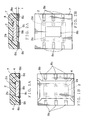
- FIGS. 1A and 1B are a sectional view of an embodiment of the semiconductor device according to this invention and a bottom view thereof;
- FIGS. 2A and 2B are a sectional view of an embodiment of the semiconductor device according to this invention and a bottom view thereof;
- FIGS. 3A, 3 B and 3 C are a plan view of a metallic substrate, a plan view of a metallic substrate with a patterned metallic layer, and an enlarged cutaway plan view of the pattern metallic layer, respectively;
- FIGS. 4A to 4 E are sectional views showing respective steps of an embodiment of a method of manufacturing a semiconductor device according to this invention.
- FIGS. 5A to 5 D are sectional views showing respective steps successive to the step of FIG. 4E in the embodiment of a method of manufacturing a semiconductor device according to this invention
- FIGS. 6A and 6B are a partially cutaway perspective view of a resin sealing body, and a bottom view of the resin sealing body, respectively;
- FIG. 7 is a bottom view of still another embodiment of a semiconductor device according to this invention.
- FIG. 8 is a sectional view of a conventional semiconductor device.
- FIGS. 1A and 1B are a sectional view of an embodiment of a leadless surface-mounted semiconductor device according to this invention and a bottom view thereof.
- reference numeral 2 denotes a semiconductor element with electrode pads formed thereon.
- Reference numeral 7 denotes a resin package for sealing the semiconductor element 2 .
- the electrode pads 2 a of the semiconductor element 2 are electrically connected to metallic layers 8 a for external extension by means of wirings 4 .
- the semiconductor element 2 is bonded to a metallic layer 8 b .
- the area of the metallic layer 8 b is wider than that of the bottom of the semiconductor element 2 .
- the semiconductor element 2 is bonded centrally to the metallic layer 8 b .
- the area of the bottom of the semiconductor element 2 is smaller than that of the metallic layer 8 b so that a sufficient creepage distance is provided between the semiconductor element 2 and the bottom of the resin package 7 .
- the bottom of the metallic layers 8 a and 8 b is exposed from the resin package 7 .
- the externally exposed planes of the metallic layers 8 a and 8 b are flush with the bottom surface of the resin package 7 .
- Flat thin-film metallic layers 8 c are formed on the bottom surfaces of the metallic layers 8 a and 8 b.
- the metallic layers 8 a and 8 each is composed of a Ni or Ni—Co thin film of nickel (Ni) or nickel-cobalt (Ni—Co) alloy which is electrically deposited on the exposed side and a gold (Au) or silver (Ag) thin film.
- the Ni or Ni—Co alloy thin film is 20-35 ⁇ m and the Au thin film is about 0.05-3 ⁇ m.
- the metallic layer 8 c is composed of a Ni or Ni—Co thin film of Ni or N—Co alloy and a Su, Au or Ag thin film.
- the Ni or Ni—Co alloy thin film is about 5 ⁇ m.
- the Sn thin film is 3-15 ⁇ m.
- the Au or Ag thin film is about 0.3 ⁇ m.
- Ni or Ni—Co thin film is deposited after a metallic film with good solderbility such as Au or Au alloy has been deposited on the surface of a metallic substrate (described later), it is not necessary to form the metallic layer 8 c.
- the semiconductor device according to this invention is not directed to a package structure in-which a semiconductor element and other elements mounted on a glass epoxy or ceramic substrate are resin-sealed, but a structure in which the semiconductor element is housed in a resin package and the metallic film is exposed from the resin package.
- the semiconductor device which does not require the substrate on which the semiconductor element is mounted, its height is low. This permits the semiconductor device to be mounted on a printed board in balance.
- the semiconductor device according to this invention has an advantage that the components are difficult to stand up when they are mounted in the printed board. Further, the semiconductor device can be mounted in the printed board in such a manner that the former is bonded to the printed board with the aid of adhesive applied to the bottom of the semiconductor device.
- FIGS. 2A and 2B are a sectional view of an embodiment of the semiconductor device according to this invention and a bottom view thereof.
- the metallic layer 8 b is thicker than the metallic layer 8 b of the semiconductor device shown in FIG. 1 and the area of the bottom of the semiconductor element 2 is larger than that of the metallic layer 8 b . Therefore, the semiconductor element 2 is sealed in the resin package 7 at the height of about 20 ⁇ m or more from the bottom of the resin package 7 .
- the semiconductor device according to this invention sufficient creepage distance is provided between the semiconductor element 2 and the bottom of the resin package 7 .
- the semiconductor element 3 having a relatively large size can be resin-sealed.
- the semiconductor device is resin-sealed so that resin is extended to the bottom of the semiconductor element 2 , a sufficient creepage distance is provided so that the semiconductor device can have high moisture resistance.
- a relatively large element can be resin-sealed in a small resin package.
- This manufacturing method is directed to a process in which a leadless surface-mounted semiconductor device is formed on a flexible planar metallic substrate and the metallic substrate is removed.
- a flexible leadless planar metallic substrate 9 is prepared.
- the metallic substrate 9 is made of thin stainless steel and 0.1 mm thick.
- the metallic substrate 9 has holes 9 a and 9 b which are used for its automated transfer and holes which are used for its securing into a mold.
- FIG. 3B shows an electrodeposition frame in which a pattern of a metallic layer on which a semiconductor element is mounted is formed.
- the semiconductor element 2 located on the one side of the metallic substrate 9 is resin-sealed so that a resin sealing body is formed on the one side of the metallic substrate.
- FIGS. 4 and 5 an explanation will be given of the first to eighth steps of a process for manufacturing a semiconductor device according to this invention.
- the first step is to electro-deposit an metallic film on the entire surface on the one side of a metallic substrate 9 of e.g. stainless steel by electrodeposition.
- a photosensitive resist film is applied on the one surface of the metallic substrate by spin coating. The entire resist film thus applied is exposed to light so that it is hardened.
- the metallic substrate 9 with a mask is immersed in an electrodeposition bath to form a metallic layer 8 on the other surface of the metallic substrate 9 .
- the metallic layer 8 is a Ni or Ni—Co alloy thin film formed by electrodeposition. Thereafter, on the Ni or Ni—Co alloy thin film, gold is deposited by vacuum deposition by flush technique or sputtering.
- a current is passed between the metallic substrate 9 and an electrode within the electrodeposition bath so that the metallic layer 8 of the Ni or Ni—Co alloy thin film.
- the Ni or No—Co alloy thin film has a thickness of e.g. 20-35 ⁇ m, and the gold thin film has a thickness of 0.3 ⁇ m.
- the subsequent step of forming an electrode metallic layer can be omitted.
- the second step is to etch the metallic layer 8 .
- a mask of a resist film 10 is formed on the one side of the metallic substrate 9 .
- Resist films 10 a and 10 b are selectively formed on the metallic layer 8 of the metallic substrate 9 .
- the metallic layer 8 is selectively etched away to form an electrodeposition frame with metallic layers 8 a and 8 b formed on the one side of the metallic substrate 9 .
- the electrodeposition frame has an area E on which a semiconductor element is to be formed and a gold wire is to be wire-bonded thereto.
- the metallic layers 8 a and 8 b are formed in a matrix shape.
- FIG. 3C shows a detailed pattern of the metallic layers.
- FIG. 3C shows the pattern of the wire-bonding area on the rear surface of a resin-sealed body (described later) when the metallic substrate is removed.
- This pattern has dicing marks 9 d and 9 c for cutting the body with a plurality of semiconductor elements resin-sealed into individual semiconductor device. In cutting, cutting lines are set between the dicing marks 9 d and 9 c.
- the third step is to mount semiconductor elements.
- semiconductor elements 2 are mounted on the metallic layers 8 b by a known technique.
- electrode pads 2 a are formed on the surface of each semiconductor element 2 .
- the manufacturing process proceeds to a fourth step which is to wire-bond gold wires 4 to the semiconductor element 2 .
- the wires 4 are electrically connected between the electrode pads 2 a of the semiconductor element 2 and the metallic layers 8 a by means of e.g. ultrasonic bonding.
- the wire bonding step of FIG. 4E is succeeded by a fifth step which is resin-molding.
- the resin-molding step is to to mount the electrodeposition frame after the semiconductor elements 2 mounted on the metallic substrate 9 have been subjected to wire bonding in a molding die (upper die) or resin sealing body 11 .
- Epoxy resin is press-fit in the cavity (not shown) formed in the molding die.
- the metallic substrate 9 serves as a lower die.
- a large number of electrodeposition frames on which the semiconductor elements are mounted are resin-sealed in such a manner that the metallic substrates on each of which the semiconductor elements are mounted are arranged in parallel, and the epoxy resin is press-fit into between the respective metallic substrates and the upper dies.
- the resin molding step is succeeded by a sixth step which is to remove the metallic substrate as shown in FIG. 5 B.
- the metallic substrate 9 is removed from the resin sealing body 11 .
- the metallic substrate 9 which is a flexible plate, can be easily removed from the resin sealing body 11 .
- the metallic layers 8 a and 8 b are exposed from the bottom of the resin sealing body 11 .
- the exposed surfaces of the metallic layers 8 a and 8 b are flush with the bottom of the resin sealing body 11 .
- the removing step is succeeded by a seventh step which is a dicing step.
- the seventh step is to dice the resin sealing body shown in FIG. 5D along dicing lines S.
- the sealing body is cut out to provide the semiconductor elements.
- the resin sealing body 11 is cut from the center line of each metallic layer 8 a between the semiconductor elements 2 to provide individual semiconductor devices.
- FIG. 6A is a partially cutaway perspective view of a resin sealing body 11 with a large number of resin-sealed semiconductor devices.
- FIG. 6B is a bottom view of the resin sealing body.
- S 1 and S 2 denote dicing lines, respectively.
- the grooves 7 a and 7 b formed in the resin sealing body 11 are cut along the dicing lines S 1 and S 2 from the bottom of the metallic substrate 9 so that the resin sealing body 11 is divided into individual semiconductor devices.
- the electrode metallic layer 8 a is cutout along the dicing line S 2 between the dicing marks M 11 and M 12 so that the adjacent metallic layers 8 a serve as the metallic layers for external extension.
- the metallic layer 8 b is cut out along the dicing line Si between dicing marks M 21 and M 22 .
- the resin sealing body 11 is divided into the individual semiconductor devices in such a manner that it is cut along the dicing lines S 1 and S 2 in the dicing step.
- the dicing step is succeeded by an eighth step of making an electrode.
- gold thin films 8 c are applied to the metallic layers 8 a and 8 b at the bottom of the resin sealing body 2 of each of the individual semiconductor devices thus diced, respectively by means of the flush technique or electrolytic or non-electrolytic plating. Further, a Ni or Ni—Co alloy thin film is deposited electrically deposited on each of the gold layers to complete an external electrode.
- the electrodeposition frame can be made not only by the technique described above but another technique. Namely, after the thin film of gold or a gold alloy on the metallic substrate has been made, it may be patterned and thereafter the thin film metallic thin film of Ni or Ni alloy may be electrically deposited thereon.
- the thin film of gold or gold alloy on the metallic substrate is selectively deposited electrically on the metallic substrate 9 in such a state where a resist film deposited on the entire surface of the metallic substrate and patterned on the other surface thereof so that the surface of the metallic substrate corresponding to the areas where the semiconductor elements are to be mounted and the metallic layers are to be formed is exposed whereas the remaining area is covered with the resist film.
- the patterned resist film is thereafter removed.
- a Ni or Ni—Co alloy film is formed on the entire surface on which the gold thin film has been formed. Thereafter, the Ni or Ni—Co alloy film is selectively removed.
- the metallic layers 8 a and 8 b are formed on the metallic substrate 9 as explained in connection with the above embodiment.
- the metallic substrate 9 is made of stainless steel having a thickness of 0.1 mm. However, this thickness should not be limited to this value.
- the metallic substrate is preferably removed from the resin sealing body with the semiconductor elements resin sealed.
- the copper substrate In the conventional semiconductor device in which the metallic substrate is made of copper, the copper substrate must be removed by etching.
- the stainless steel substrate can be easily removed from the resin sealing body.
- the stainless steel may be any one of SUS in the system of notation in the Japanese Industrial Standards.
- the semiconductor device as shown in FIG. 2 is manufactured in which the metallic layer 8 b on which the semiconductor element 2 is mounted is thicker than the metallic layer 8 a , after the metallic layer 8 a has been formed on the metallic substrate, with a resist mask for forming the metallic layer 8 b , the metallic substrate is immersed for electrodeposition for the metallic layer 8 b in a longer time than the time taken for electrodeposition of the metallic layer 8 a .
- the subsequent steps have been described above.
- the metallic layers 13 exposed from the resin package 7 have a flat surface, and the electrode pads 2 a of the semiconductor element 2 sealed in the resin package 7 are electrically connected to the metallic layers 13 by means of wires 4 .
- the semiconductor elements are sealed in resin package so that the metallic layers for external extension are exposed from the bottom of the resin package.
- the bottom of the resin package is flush with that of the metallic layers for external extension.
- the Ni or Ni—Co alloy thin film and the Au thin film are formed on the metallic layers as external electrodes.
- the external electrodes protrude slightly from the bottom of the resin package.
Landscapes
- Engineering & Computer Science (AREA)
- Computer Hardware Design (AREA)
- Microelectronics & Electronic Packaging (AREA)
- Power Engineering (AREA)
- Physics & Mathematics (AREA)
- Condensed Matter Physics & Semiconductors (AREA)
- General Physics & Mathematics (AREA)
- Manufacturing & Machinery (AREA)
- Encapsulation Of And Coatings For Semiconductor Or Solid State Devices (AREA)
- Structures Or Materials For Encapsulating Or Coating Semiconductor Devices Or Solid State Devices (AREA)
- Lead Frames For Integrated Circuits (AREA)
Applications Claiming Priority (4)
| Application Number | Priority Date | Filing Date | Title |
|---|---|---|---|
| JP2000-124102 | 2000-04-25 | ||
| JP2000124102 | 2000-04-25 | ||
| JP2001078791A JP2002016181A (ja) | 2000-04-25 | 2001-03-19 | 半導体装置、その製造方法、及び電着フレーム |
| JP2001-078791 | 2001-03-19 |
Publications (2)
| Publication Number | Publication Date |
|---|---|
| US20010033018A1 US20010033018A1 (en) | 2001-10-25 |
| US6800508B2 true US6800508B2 (en) | 2004-10-05 |
Family
ID=26590739
Family Applications (1)
| Application Number | Title | Priority Date | Filing Date |
|---|---|---|---|
| US09/837,022 Expired - Lifetime US6800508B2 (en) | 2000-04-25 | 2001-04-18 | Semiconductor device, its manufacturing method and electrodeposition frame |
Country Status (3)
| Country | Link |
|---|---|
| US (1) | US6800508B2 (ja) |
| JP (1) | JP2002016181A (ja) |
| TW (1) | TW493254B (ja) |
Cited By (16)
| Publication number | Priority date | Publication date | Assignee | Title |
|---|---|---|---|---|
| US20040115919A1 (en) * | 2001-05-14 | 2004-06-17 | Yuji Takaoka | Semiconductor device and its manufacturing method |
| US20050012026A1 (en) * | 2003-07-16 | 2005-01-20 | Jackson Hsieh | Image sensor and method for packaging the same |
| US20050012027A1 (en) * | 2003-07-16 | 2005-01-20 | Jackson Hsieh | Image sensor and method for packaging the same |
| US20050012025A1 (en) * | 2003-07-16 | 2005-01-20 | Jackson Hsieh | Image sensor and method for packaging the same |
| US20050032271A1 (en) * | 2001-05-30 | 2005-02-10 | Nec Electronics Corporation | Lead frame, semiconductor device using the same and method of producing the semiconductor device |
| US20050287709A1 (en) * | 2004-06-23 | 2005-12-29 | Advanced Semiconductor Engineering Inc. | Process for manufacturing leadless semiconductor packages including an electrical test in a matrix of a leadless leadframe |
| US20060211233A1 (en) * | 2005-03-21 | 2006-09-21 | Skyworks Solutions, Inc. | Method for fabricating a wafer level package having through wafer vias for external package connectivity and related structure |
| US20060220173A1 (en) * | 2005-04-01 | 2006-10-05 | Skyworks Solutions, Inc. | Wafer level package including a device wafer integrated with a passive component |
| US20080012098A1 (en) * | 2006-07-17 | 2008-01-17 | Stats Chippac Ltd. | Integrated circuit package system employing an exposed thermally conductive coating |
| US20080217708A1 (en) * | 2007-03-09 | 2008-09-11 | Skyworks Solutions, Inc. | Integrated passive cap in a system-in-package |
| US20090029526A1 (en) * | 2007-07-24 | 2009-01-29 | Northrop Grumman Space & Mission Systems Corp. | Method of Exposing Circuit Lateral Interconnect Contacts by Wafer Saw |
| US20090075431A1 (en) * | 2006-08-02 | 2009-03-19 | Skyworks Solutions, Inc. | Wafer level package with cavities for active devices |
| US20100120201A1 (en) * | 2008-11-07 | 2010-05-13 | Chipmos Technologies Inc. | Method of fabricating quad flat non-leaded package |
| US20100244161A1 (en) * | 2007-11-30 | 2010-09-30 | Skyworks Solutions, Inc. | Wafer level packaging using flip chip mounting |
| US20100283144A1 (en) * | 2007-12-26 | 2010-11-11 | Steve Xin Liang | In-situ cavity circuit package |
| US20150028360A1 (en) * | 2013-07-25 | 2015-01-29 | Lingsen Precision Industries, Ltd. | Package structure of optical module |
Families Citing this family (25)
| Publication number | Priority date | Publication date | Assignee | Title |
|---|---|---|---|---|
| KR100868419B1 (ko) | 2001-06-07 | 2008-11-11 | 가부시끼가이샤 르네사스 테크놀로지 | 반도체장치 및 그 제조방법 |
| JP3942457B2 (ja) | 2002-02-27 | 2007-07-11 | Necエレクトロニクス株式会社 | 電子部品の製造方法 |
| JP2004214265A (ja) * | 2002-12-27 | 2004-07-29 | Kyushu Hitachi Maxell Ltd | 半導体装置および半導体装置の製造方法 |
| JP2006093575A (ja) * | 2004-09-27 | 2006-04-06 | Hitachi Cable Ltd | 半導体装置およびその製造方法 |
| JP2006310570A (ja) * | 2005-04-28 | 2006-11-09 | Aoi Electronics Co Ltd | 半導体装置 |
| JP4549318B2 (ja) * | 2006-06-29 | 2010-09-22 | アオイ電子株式会社 | 半導体装置および半導体装置の製造方法 |
| KR100893567B1 (ko) * | 2007-08-14 | 2009-04-17 | 앰코 테크놀로지 코리아 주식회사 | 반도체 패키지 제조 방법 |
| US7825514B2 (en) | 2007-12-11 | 2010-11-02 | Dai Nippon Printing Co., Ltd. | Substrate for semiconductor device, resin-sealed semiconductor device, method for manufacturing said substrate for semiconductor device and method for manufacturing said resin-sealed semiconductor device |
| JP2009170476A (ja) * | 2008-01-11 | 2009-07-30 | Panasonic Corp | 半導体装置および半導体装置の製造方法 |
| JP5167022B2 (ja) * | 2008-08-07 | 2013-03-21 | ルネサスエレクトロニクス株式会社 | 半導体装置の製造方法 |
| WO2010045594A2 (en) * | 2008-10-17 | 2010-04-22 | Occam Portfolio Llc | Flexible circuit assemblies without solder and methods for their manufacture |
| US20100184241A1 (en) * | 2009-01-16 | 2010-07-22 | Edison Opto Corporation | Method for manufacturing thin type light emitting diode assembly |
| US8866296B2 (en) | 2009-06-24 | 2014-10-21 | Aoi Electronics Co., Ltd. | Semiconductor device comprising thin-film terminal with deformed portion |
| JP6146732B2 (ja) * | 2013-01-18 | 2017-06-14 | Shマテリアル株式会社 | 半導体素子搭載用基板及びその製造方法 |
| JP5801339B2 (ja) * | 2013-03-22 | 2015-10-28 | 株式会社東芝 | 半導体装置 |
| JP2013168686A (ja) * | 2013-06-03 | 2013-08-29 | Hitachi Maxell Ltd | 半導体装置および半導体装置の製造方法 |
| JP5807815B2 (ja) * | 2013-11-01 | 2015-11-10 | 大日本印刷株式会社 | 半導体装置およびその製造方法、ならびに半導体装置用基板およびその製造方法 |
| JP2014053638A (ja) * | 2013-11-15 | 2014-03-20 | Dainippon Printing Co Ltd | 半導体装置およびその製造方法、ならびに半導体装置用基板およびその製造方法 |
| JP2015233166A (ja) * | 2015-10-01 | 2015-12-24 | 日立マクセル株式会社 | 半導体装置および半導体装置の製造方法 |
| JP2017005261A (ja) * | 2016-08-22 | 2017-01-05 | 日立マクセル株式会社 | 半導体装置および半導体装置の製造方法 |
| JP2017118131A (ja) * | 2017-02-13 | 2017-06-29 | 日立マクセル株式会社 | 半導体装置用中間部品およびその製造方法、並びに半導体装置およびその製造方法 |
| JP2017195414A (ja) * | 2017-07-20 | 2017-10-26 | 日立マクセル株式会社 | 半導体装置および半導体装置の製造方法 |
| JP2018029214A (ja) * | 2017-11-24 | 2018-02-22 | マクセルホールディングス株式会社 | 半導体装置および半導体装置の製造方法 |
| JP2018160707A (ja) * | 2018-07-23 | 2018-10-11 | マクセルホールディングス株式会社 | 半導体装置および半導体装置の製造方法 |
| JP2019096901A (ja) * | 2019-02-06 | 2019-06-20 | マクセルホールディングス株式会社 | 半導体装置および半導体装置の製造方法 |
Citations (19)
| Publication number | Priority date | Publication date | Assignee | Title |
|---|---|---|---|---|
| US633252A (en) * | 1898-10-19 | 1899-09-19 | Vincenzo Venezia | Floor and ceiling for buildings. |
| US3698076A (en) * | 1970-08-03 | 1972-10-17 | Motorola Inc | Method of applying leads to an integrated circuit |
| US4033833A (en) * | 1975-10-30 | 1977-07-05 | Western Electric Company, Inc. | Method of selectively electroplating an area of a surface |
| JPH03108745A (ja) * | 1989-09-22 | 1991-05-08 | Seiko Epson Corp | 半導体装置 |
| JPH06188349A (ja) * | 1992-12-18 | 1994-07-08 | Kyushu Hitachi Maxell Ltd | 電鋳製のic用リードフレーム並びにその製造方法 |
| JPH09148508A (ja) * | 1995-11-29 | 1997-06-06 | Nippon Denkai Kk | 半導体装置用リードフレーム及びこれを用いた樹脂封止型半導体装置 |
| US5900676A (en) * | 1996-08-19 | 1999-05-04 | Samsung Electronics Co., Ltd. | Semiconductor device package structure having column leads and a method for production thereof |
| US5909053A (en) * | 1992-12-23 | 1999-06-01 | Shinko Electric Industries Co. Ltd. | Lead frame and method for manufacturing same |
| US6001671A (en) * | 1996-04-18 | 1999-12-14 | Tessera, Inc. | Methods for manufacturing a semiconductor package having a sacrificial layer |
| US6166430A (en) * | 1998-05-27 | 2000-12-26 | Matsushita Electronics Corporation | Lead frame, method for manufacturing the frame, resin-molded semiconductor device and method for manufacturing the device |
| JP2001024001A (ja) * | 1999-07-12 | 2001-01-26 | Matsushita Electronics Industry Corp | 樹脂封止型半導体装置の製造方法及びリードフレーム |
| US6191494B1 (en) * | 1998-06-30 | 2001-02-20 | Fujitsu Limited | Semiconductor device and method of producing the same |
| US6211462B1 (en) * | 1998-11-05 | 2001-04-03 | Texas Instruments Incorporated | Low inductance power package for integrated circuits |
| US6247229B1 (en) * | 1999-08-25 | 2001-06-19 | Ankor Technology, Inc. | Method of forming an integrated circuit device package using a plastic tape as a base |
| US6333252B1 (en) * | 2000-01-05 | 2001-12-25 | Advanced Semiconductor Engineering, Inc. | Low-pin-count chip package and manufacturing method thereof |
| US6365980B1 (en) * | 1999-02-26 | 2002-04-02 | Texas Instruments Incorporated | Thermally enhanced semiconductor ball grid array device and method of fabrication |
| US6380062B1 (en) * | 2001-03-09 | 2002-04-30 | Walsin Advanced Electronics Ltd. | Method of fabricating semiconductor package having metal peg leads and connected by trace lines |
| US20020100165A1 (en) * | 2000-02-14 | 2002-08-01 | Amkor Technology, Inc. | Method of forming an integrated circuit device package using a temporary substrate |
| US20020197256A1 (en) * | 2001-04-02 | 2002-12-26 | Genentech, Inc. | Combination therapy |
-
2001
- 2001-03-19 JP JP2001078791A patent/JP2002016181A/ja not_active Withdrawn
- 2001-04-18 TW TW090109265A patent/TW493254B/zh not_active IP Right Cessation
- 2001-04-18 US US09/837,022 patent/US6800508B2/en not_active Expired - Lifetime
Patent Citations (19)
| Publication number | Priority date | Publication date | Assignee | Title |
|---|---|---|---|---|
| US633252A (en) * | 1898-10-19 | 1899-09-19 | Vincenzo Venezia | Floor and ceiling for buildings. |
| US3698076A (en) * | 1970-08-03 | 1972-10-17 | Motorola Inc | Method of applying leads to an integrated circuit |
| US4033833A (en) * | 1975-10-30 | 1977-07-05 | Western Electric Company, Inc. | Method of selectively electroplating an area of a surface |
| JPH03108745A (ja) * | 1989-09-22 | 1991-05-08 | Seiko Epson Corp | 半導体装置 |
| JPH06188349A (ja) * | 1992-12-18 | 1994-07-08 | Kyushu Hitachi Maxell Ltd | 電鋳製のic用リードフレーム並びにその製造方法 |
| US5909053A (en) * | 1992-12-23 | 1999-06-01 | Shinko Electric Industries Co. Ltd. | Lead frame and method for manufacturing same |
| JPH09148508A (ja) * | 1995-11-29 | 1997-06-06 | Nippon Denkai Kk | 半導体装置用リードフレーム及びこれを用いた樹脂封止型半導体装置 |
| US6001671A (en) * | 1996-04-18 | 1999-12-14 | Tessera, Inc. | Methods for manufacturing a semiconductor package having a sacrificial layer |
| US5900676A (en) * | 1996-08-19 | 1999-05-04 | Samsung Electronics Co., Ltd. | Semiconductor device package structure having column leads and a method for production thereof |
| US6166430A (en) * | 1998-05-27 | 2000-12-26 | Matsushita Electronics Corporation | Lead frame, method for manufacturing the frame, resin-molded semiconductor device and method for manufacturing the device |
| US6191494B1 (en) * | 1998-06-30 | 2001-02-20 | Fujitsu Limited | Semiconductor device and method of producing the same |
| US6211462B1 (en) * | 1998-11-05 | 2001-04-03 | Texas Instruments Incorporated | Low inductance power package for integrated circuits |
| US6365980B1 (en) * | 1999-02-26 | 2002-04-02 | Texas Instruments Incorporated | Thermally enhanced semiconductor ball grid array device and method of fabrication |
| JP2001024001A (ja) * | 1999-07-12 | 2001-01-26 | Matsushita Electronics Industry Corp | 樹脂封止型半導体装置の製造方法及びリードフレーム |
| US6247229B1 (en) * | 1999-08-25 | 2001-06-19 | Ankor Technology, Inc. | Method of forming an integrated circuit device package using a plastic tape as a base |
| US6333252B1 (en) * | 2000-01-05 | 2001-12-25 | Advanced Semiconductor Engineering, Inc. | Low-pin-count chip package and manufacturing method thereof |
| US20020100165A1 (en) * | 2000-02-14 | 2002-08-01 | Amkor Technology, Inc. | Method of forming an integrated circuit device package using a temporary substrate |
| US6380062B1 (en) * | 2001-03-09 | 2002-04-30 | Walsin Advanced Electronics Ltd. | Method of fabricating semiconductor package having metal peg leads and connected by trace lines |
| US20020197256A1 (en) * | 2001-04-02 | 2002-12-26 | Genentech, Inc. | Combination therapy |
Cited By (33)
| Publication number | Priority date | Publication date | Assignee | Title |
|---|---|---|---|---|
| US7064005B2 (en) * | 2001-05-14 | 2006-06-20 | Sony Corporation | Semiconductor apparatus and method of manufacturing same |
| US20040115919A1 (en) * | 2001-05-14 | 2004-06-17 | Yuji Takaoka | Semiconductor device and its manufacturing method |
| US20050032271A1 (en) * | 2001-05-30 | 2005-02-10 | Nec Electronics Corporation | Lead frame, semiconductor device using the same and method of producing the semiconductor device |
| US7189599B2 (en) * | 2001-05-30 | 2007-03-13 | Nec Electronics Corporation | Lead frame, semiconductor device using the same and method of producing the semiconductor device |
| US20050012026A1 (en) * | 2003-07-16 | 2005-01-20 | Jackson Hsieh | Image sensor and method for packaging the same |
| US20050012027A1 (en) * | 2003-07-16 | 2005-01-20 | Jackson Hsieh | Image sensor and method for packaging the same |
| US20050012025A1 (en) * | 2003-07-16 | 2005-01-20 | Jackson Hsieh | Image sensor and method for packaging the same |
| US20050287709A1 (en) * | 2004-06-23 | 2005-12-29 | Advanced Semiconductor Engineering Inc. | Process for manufacturing leadless semiconductor packages including an electrical test in a matrix of a leadless leadframe |
| US7125747B2 (en) * | 2004-06-23 | 2006-10-24 | Advanced Semiconductor Engineering, Inc. | Process for manufacturing leadless semiconductor packages including an electrical test in a matrix of a leadless leadframe |
| US20080064142A1 (en) * | 2005-03-21 | 2008-03-13 | Skyworks Solutions, Inc. | Method for fabricating a wafer level package having through wafer vias for external package connectivity |
| US20060211233A1 (en) * | 2005-03-21 | 2006-09-21 | Skyworks Solutions, Inc. | Method for fabricating a wafer level package having through wafer vias for external package connectivity and related structure |
| US20060220173A1 (en) * | 2005-04-01 | 2006-10-05 | Skyworks Solutions, Inc. | Wafer level package including a device wafer integrated with a passive component |
| US20080003761A1 (en) * | 2005-04-01 | 2008-01-03 | Skyworks Solutions, Inc. | Method for fabricating a wafer level package with device wafer and passive component integration |
| US7629201B2 (en) | 2005-04-01 | 2009-12-08 | Skyworks Solutions, Inc. | Method for fabricating a wafer level package with device wafer and passive component integration |
| US7576426B2 (en) | 2005-04-01 | 2009-08-18 | Skyworks Solutions, Inc. | Wafer level package including a device wafer integrated with a passive component |
| US20080012098A1 (en) * | 2006-07-17 | 2008-01-17 | Stats Chippac Ltd. | Integrated circuit package system employing an exposed thermally conductive coating |
| US8124460B2 (en) * | 2006-07-17 | 2012-02-28 | Stats Chippac Ltd. | Integrated circuit package system employing an exposed thermally conductive coating |
| US20090075431A1 (en) * | 2006-08-02 | 2009-03-19 | Skyworks Solutions, Inc. | Wafer level package with cavities for active devices |
| US7635606B2 (en) * | 2006-08-02 | 2009-12-22 | Skyworks Solutions, Inc. | Wafer level package with cavities for active devices |
| US20080217708A1 (en) * | 2007-03-09 | 2008-09-11 | Skyworks Solutions, Inc. | Integrated passive cap in a system-in-package |
| US7662669B2 (en) | 2007-07-24 | 2010-02-16 | Northrop Grumman Space & Mission Systems Corp. | Method of exposing circuit lateral interconnect contacts by wafer saw |
| US20090029526A1 (en) * | 2007-07-24 | 2009-01-29 | Northrop Grumman Space & Mission Systems Corp. | Method of Exposing Circuit Lateral Interconnect Contacts by Wafer Saw |
| US20100244161A1 (en) * | 2007-11-30 | 2010-09-30 | Skyworks Solutions, Inc. | Wafer level packaging using flip chip mounting |
| US8324728B2 (en) | 2007-11-30 | 2012-12-04 | Skyworks Solutions, Inc. | Wafer level packaging using flip chip mounting |
| US8809116B2 (en) | 2007-11-30 | 2014-08-19 | Skyworks Solutions, Inc. | Method for wafer level packaging of electronic devices |
| US8900931B2 (en) | 2007-12-26 | 2014-12-02 | Skyworks Solutions, Inc. | In-situ cavity integrated circuit package |
| US20100283144A1 (en) * | 2007-12-26 | 2010-11-11 | Steve Xin Liang | In-situ cavity circuit package |
| US9153551B2 (en) | 2007-12-26 | 2015-10-06 | Skyworks Solutions, Inc. | Integrated circuit package including in-situ formed cavity |
| US20100120201A1 (en) * | 2008-11-07 | 2010-05-13 | Chipmos Technologies Inc. | Method of fabricating quad flat non-leaded package |
| US7842550B2 (en) * | 2008-11-07 | 2010-11-30 | Chipmos Technologies Inc. | Method of fabricating quad flat non-leaded package |
| US20150028360A1 (en) * | 2013-07-25 | 2015-01-29 | Lingsen Precision Industries, Ltd. | Package structure of optical module |
| US20150091024A1 (en) * | 2013-07-25 | 2015-04-02 | Lingsen Precision Industries, Ltd. | Package structure of optical module |
| US9190398B2 (en) * | 2013-07-25 | 2015-11-17 | Lingsen Precision Industries, Ltd. | Method for packaging an optical module |
Also Published As
| Publication number | Publication date |
|---|---|
| US20010033018A1 (en) | 2001-10-25 |
| JP2002016181A (ja) | 2002-01-18 |
| TW493254B (en) | 2002-07-01 |
Similar Documents
| Publication | Publication Date | Title |
|---|---|---|
| US6800508B2 (en) | Semiconductor device, its manufacturing method and electrodeposition frame | |
| KR101037997B1 (ko) | 반도체 다이 패키지와 반도체 다이 패키지용 기판 그리고 이들의 형성 방법, 및 리드 프레임 구조물의 제조 방법 및 처리 방법 | |
| US6429508B1 (en) | Semiconductor package having implantable conductive lands and method for manufacturing the same | |
| KR100639738B1 (ko) | 회로 장치의 제조 방법 | |
| US6933594B2 (en) | Leadless plastic chip carrier with etch back pad singulation | |
| US5756377A (en) | Lead frame and manufacturing method thereof | |
| US6995460B1 (en) | Leadless plastic chip carrier with etch back pad singulation | |
| US5859471A (en) | Semiconductor device having tab tape lead frame with reinforced outer leads | |
| KR100294719B1 (ko) | 수지밀봉형 반도체장치 및 그 제조방법, 리드프레임 | |
| US6548328B1 (en) | Circuit device and manufacturing method of circuit device | |
| US7271032B1 (en) | Leadless plastic chip carrier with etch back pad singulation | |
| KR20040030297A (ko) | 리드 프레임, 그 리드 프레임의 제조 방법, 및 반도체 장치 | |
| KR20040030283A (ko) | 리드 프레임 및 그 제조 방법 | |
| US7550322B2 (en) | Manufacturing method for resin sealed semiconductor device | |
| KR20020075188A (ko) | 회로 장치의 제조 방법 | |
| JP3869849B2 (ja) | 半導体装置の製造方法 | |
| US20040262752A1 (en) | Semiconductor device | |
| JP2005286057A (ja) | 回路装置およびその製造方法 | |
| US7443043B2 (en) | Circuit device and method of manufacture thereof | |
| JP4679000B2 (ja) | 板状体 | |
| US6455786B1 (en) | Wiring board and manufacturing method thereof and semiconductor device | |
| JP3394696B2 (ja) | 半導体装置及びその製造方法 | |
| JPH11176856A (ja) | 半導体装置の製造方法 | |
| JP4663172B2 (ja) | 半導体装置の製造方法 | |
| JP3778783B2 (ja) | 回路装置およびその製造方法 |
Legal Events
| Date | Code | Title | Description |
|---|---|---|---|
| AS | Assignment |
Owner name: TOREX SEMICONDUCTOR LTD, JAPAN Free format text: ASSIGNMENT OF ASSIGNORS INTEREST;ASSIGNOR:KIMURA, HIROSHI;REEL/FRAME:012012/0420 Effective date: 20010411 |
|
| STCF | Information on status: patent grant |
Free format text: PATENTED CASE |
|
| FEPP | Fee payment procedure |
Free format text: PAT HOLDER CLAIMS SMALL ENTITY STATUS, ENTITY STATUS SET TO SMALL (ORIGINAL EVENT CODE: LTOS); ENTITY STATUS OF PATENT OWNER: SMALL ENTITY |
|
| FPAY | Fee payment |
Year of fee payment: 4 |
|
| REMI | Maintenance fee reminder mailed | ||
| FPAY | Fee payment |
Year of fee payment: 8 |
|
| FPAY | Fee payment |
Year of fee payment: 12 |