US7576426B2 - Wafer level package including a device wafer integrated with a passive component - Google Patents
Wafer level package including a device wafer integrated with a passive component Download PDFInfo
- Publication number
- US7576426B2 US7576426B2 US11/097,646 US9764605A US7576426B2 US 7576426 B2 US7576426 B2 US 7576426B2 US 9764605 A US9764605 A US 9764605A US 7576426 B2 US7576426 B2 US 7576426B2
- Authority
- US
- United States
- Prior art keywords
- polymer layer
- wafer
- level package
- device wafer
- wafer level
- Prior art date
- Legal status (The legal status is an assumption and is not a legal conclusion. Google has not performed a legal analysis and makes no representation as to the accuracy of the status listed.)
- Active, expires
Links
Images


Classifications
-
- H—ELECTRICITY
- H01—ELECTRIC ELEMENTS
- H01L—SEMICONDUCTOR DEVICES NOT COVERED BY CLASS H10
- H01L23/00—Details of semiconductor or other solid state devices
- H01L23/48—Arrangements for conducting electric current to or from the solid state body in operation, e.g. leads, terminal arrangements ; Selection of materials therefor
- H01L23/488—Arrangements for conducting electric current to or from the solid state body in operation, e.g. leads, terminal arrangements ; Selection of materials therefor consisting of soldered or bonded constructions
- H01L23/498—Leads, i.e. metallisations or lead-frames on insulating substrates, e.g. chip carriers
- H01L23/49822—Multilayer substrates
-
- H—ELECTRICITY
- H01—ELECTRIC ELEMENTS
- H01L—SEMICONDUCTOR DEVICES NOT COVERED BY CLASS H10
- H01L23/00—Details of semiconductor or other solid state devices
- H01L23/48—Arrangements for conducting electric current to or from the solid state body in operation, e.g. leads, terminal arrangements ; Selection of materials therefor
-
- B—PERFORMING OPERATIONS; TRANSPORTING
- B81—MICROSTRUCTURAL TECHNOLOGY
- B81C—PROCESSES OR APPARATUS SPECIALLY ADAPTED FOR THE MANUFACTURE OR TREATMENT OF MICROSTRUCTURAL DEVICES OR SYSTEMS
- B81C1/00—Manufacture or treatment of devices or systems in or on a substrate
- B81C1/00015—Manufacture or treatment of devices or systems in or on a substrate for manufacturing microsystems
- B81C1/00261—Processes for packaging MEMS devices
- B81C1/00269—Bonding of solid lids or wafers to the substrate
-
- H—ELECTRICITY
- H01—ELECTRIC ELEMENTS
- H01L—SEMICONDUCTOR DEVICES NOT COVERED BY CLASS H10
- H01L21/00—Processes or apparatus adapted for the manufacture or treatment of semiconductor or solid state devices or of parts thereof
- H01L21/02—Manufacture or treatment of semiconductor devices or of parts thereof
- H01L21/04—Manufacture or treatment of semiconductor devices or of parts thereof the devices having at least one potential-jump barrier or surface barrier, e.g. PN junction, depletion layer or carrier concentration layer
- H01L21/34—Manufacture or treatment of semiconductor devices or of parts thereof the devices having at least one potential-jump barrier or surface barrier, e.g. PN junction, depletion layer or carrier concentration layer the devices having semiconductor bodies not provided for in groups H01L21/0405, H01L21/0445, H01L21/06, H01L21/16 and H01L21/18 with or without impurities, e.g. doping materials
- H01L21/44—Manufacture of electrodes on semiconductor bodies using processes or apparatus not provided for in groups H01L21/38 - H01L21/428
-
- H—ELECTRICITY
- H01—ELECTRIC ELEMENTS
- H01L—SEMICONDUCTOR DEVICES NOT COVERED BY CLASS H10
- H01L21/00—Processes or apparatus adapted for the manufacture or treatment of semiconductor or solid state devices or of parts thereof
- H01L21/02—Manufacture or treatment of semiconductor devices or of parts thereof
- H01L21/04—Manufacture or treatment of semiconductor devices or of parts thereof the devices having at least one potential-jump barrier or surface barrier, e.g. PN junction, depletion layer or carrier concentration layer
- H01L21/48—Manufacture or treatment of parts, e.g. containers, prior to assembly of the devices, using processes not provided for in a single one of the subgroups H01L21/06 - H01L21/326
- H01L21/4814—Conductive parts
- H01L21/4846—Leads on or in insulating or insulated substrates, e.g. metallisation
- H01L21/4857—Multilayer substrates
-
- H—ELECTRICITY
- H01—ELECTRIC ELEMENTS
- H01L—SEMICONDUCTOR DEVICES NOT COVERED BY CLASS H10
- H01L21/00—Processes or apparatus adapted for the manufacture or treatment of semiconductor or solid state devices or of parts thereof
- H01L21/67—Apparatus specially adapted for handling semiconductor or electric solid state devices during manufacture or treatment thereof; Apparatus specially adapted for handling wafers during manufacture or treatment of semiconductor or electric solid state devices or components ; Apparatus not specifically provided for elsewhere
- H01L21/683—Apparatus specially adapted for handling semiconductor or electric solid state devices during manufacture or treatment thereof; Apparatus specially adapted for handling wafers during manufacture or treatment of semiconductor or electric solid state devices or components ; Apparatus not specifically provided for elsewhere for supporting or gripping
- H01L21/6835—Apparatus specially adapted for handling semiconductor or electric solid state devices during manufacture or treatment thereof; Apparatus specially adapted for handling wafers during manufacture or treatment of semiconductor or electric solid state devices or components ; Apparatus not specifically provided for elsewhere for supporting or gripping using temporarily an auxiliary support
-
- H—ELECTRICITY
- H01—ELECTRIC ELEMENTS
- H01L—SEMICONDUCTOR DEVICES NOT COVERED BY CLASS H10
- H01L23/00—Details of semiconductor or other solid state devices
- H01L23/12—Mountings, e.g. non-detachable insulating substrates
-
- H—ELECTRICITY
- H01—ELECTRIC ELEMENTS
- H01L—SEMICONDUCTOR DEVICES NOT COVERED BY CLASS H10
- H01L24/00—Arrangements for connecting or disconnecting semiconductor or solid-state bodies; Methods or apparatus related thereto
- H01L24/73—Means for bonding being of different types provided for in two or more of groups H01L24/10, H01L24/18, H01L24/26, H01L24/34, H01L24/42, H01L24/50, H01L24/63, H01L24/71
-
- H—ELECTRICITY
- H01—ELECTRIC ELEMENTS
- H01L—SEMICONDUCTOR DEVICES NOT COVERED BY CLASS H10
- H01L2221/00—Processes or apparatus adapted for the manufacture or treatment of semiconductor or solid state devices or of parts thereof covered by H01L21/00
- H01L2221/67—Apparatus for handling semiconductor or electric solid state devices during manufacture or treatment thereof; Apparatus for handling wafers during manufacture or treatment of semiconductor or electric solid state devices or components; Apparatus not specifically provided for elsewhere
- H01L2221/683—Apparatus for handling semiconductor or electric solid state devices during manufacture or treatment thereof; Apparatus for handling wafers during manufacture or treatment of semiconductor or electric solid state devices or components; Apparatus not specifically provided for elsewhere for supporting or gripping
- H01L2221/68304—Apparatus for handling semiconductor or electric solid state devices during manufacture or treatment thereof; Apparatus for handling wafers during manufacture or treatment of semiconductor or electric solid state devices or components; Apparatus not specifically provided for elsewhere for supporting or gripping using temporarily an auxiliary support
- H01L2221/68327—Apparatus for handling semiconductor or electric solid state devices during manufacture or treatment thereof; Apparatus for handling wafers during manufacture or treatment of semiconductor or electric solid state devices or components; Apparatus not specifically provided for elsewhere for supporting or gripping using temporarily an auxiliary support used during dicing or grinding
-
- H—ELECTRICITY
- H01—ELECTRIC ELEMENTS
- H01L—SEMICONDUCTOR DEVICES NOT COVERED BY CLASS H10
- H01L2221/00—Processes or apparatus adapted for the manufacture or treatment of semiconductor or solid state devices or of parts thereof covered by H01L21/00
- H01L2221/67—Apparatus for handling semiconductor or electric solid state devices during manufacture or treatment thereof; Apparatus for handling wafers during manufacture or treatment of semiconductor or electric solid state devices or components; Apparatus not specifically provided for elsewhere
- H01L2221/683—Apparatus for handling semiconductor or electric solid state devices during manufacture or treatment thereof; Apparatus for handling wafers during manufacture or treatment of semiconductor or electric solid state devices or components; Apparatus not specifically provided for elsewhere for supporting or gripping
- H01L2221/68304—Apparatus for handling semiconductor or electric solid state devices during manufacture or treatment thereof; Apparatus for handling wafers during manufacture or treatment of semiconductor or electric solid state devices or components; Apparatus not specifically provided for elsewhere for supporting or gripping using temporarily an auxiliary support
- H01L2221/68345—Apparatus for handling semiconductor or electric solid state devices during manufacture or treatment thereof; Apparatus for handling wafers during manufacture or treatment of semiconductor or electric solid state devices or components; Apparatus not specifically provided for elsewhere for supporting or gripping using temporarily an auxiliary support used as a support during the manufacture of self supporting substrates
-
- H—ELECTRICITY
- H01—ELECTRIC ELEMENTS
- H01L—SEMICONDUCTOR DEVICES NOT COVERED BY CLASS H10
- H01L2224/00—Indexing scheme for arrangements for connecting or disconnecting semiconductor or solid-state bodies and methods related thereto as covered by H01L24/00
- H01L2224/01—Means for bonding being attached to, or being formed on, the surface to be connected, e.g. chip-to-package, die-attach, "first-level" interconnects; Manufacturing methods related thereto
- H01L2224/02—Bonding areas; Manufacturing methods related thereto
- H01L2224/04—Structure, shape, material or disposition of the bonding areas prior to the connecting process
- H01L2224/0401—Bonding areas specifically adapted for bump connectors, e.g. under bump metallisation [UBM]
-
- H—ELECTRICITY
- H01—ELECTRIC ELEMENTS
- H01L—SEMICONDUCTOR DEVICES NOT COVERED BY CLASS H10
- H01L2224/00—Indexing scheme for arrangements for connecting or disconnecting semiconductor or solid-state bodies and methods related thereto as covered by H01L24/00
- H01L2224/01—Means for bonding being attached to, or being formed on, the surface to be connected, e.g. chip-to-package, die-attach, "first-level" interconnects; Manufacturing methods related thereto
- H01L2224/02—Bonding areas; Manufacturing methods related thereto
- H01L2224/04—Structure, shape, material or disposition of the bonding areas prior to the connecting process
- H01L2224/04026—Bonding areas specifically adapted for layer connectors
-
- H—ELECTRICITY
- H01—ELECTRIC ELEMENTS
- H01L—SEMICONDUCTOR DEVICES NOT COVERED BY CLASS H10
- H01L2224/00—Indexing scheme for arrangements for connecting or disconnecting semiconductor or solid-state bodies and methods related thereto as covered by H01L24/00
- H01L2224/01—Means for bonding being attached to, or being formed on, the surface to be connected, e.g. chip-to-package, die-attach, "first-level" interconnects; Manufacturing methods related thereto
- H01L2224/02—Bonding areas; Manufacturing methods related thereto
- H01L2224/04—Structure, shape, material or disposition of the bonding areas prior to the connecting process
- H01L2224/05—Structure, shape, material or disposition of the bonding areas prior to the connecting process of an individual bonding area
- H01L2224/0554—External layer
- H01L2224/0556—Disposition
- H01L2224/05568—Disposition the whole external layer protruding from the surface
-
- H—ELECTRICITY
- H01—ELECTRIC ELEMENTS
- H01L—SEMICONDUCTOR DEVICES NOT COVERED BY CLASS H10
- H01L2224/00—Indexing scheme for arrangements for connecting or disconnecting semiconductor or solid-state bodies and methods related thereto as covered by H01L24/00
- H01L2224/01—Means for bonding being attached to, or being formed on, the surface to be connected, e.g. chip-to-package, die-attach, "first-level" interconnects; Manufacturing methods related thereto
- H01L2224/02—Bonding areas; Manufacturing methods related thereto
- H01L2224/04—Structure, shape, material or disposition of the bonding areas prior to the connecting process
- H01L2224/05—Structure, shape, material or disposition of the bonding areas prior to the connecting process of an individual bonding area
- H01L2224/0554—External layer
- H01L2224/05573—Single external layer
-
- H—ELECTRICITY
- H01—ELECTRIC ELEMENTS
- H01L—SEMICONDUCTOR DEVICES NOT COVERED BY CLASS H10
- H01L2224/00—Indexing scheme for arrangements for connecting or disconnecting semiconductor or solid-state bodies and methods related thereto as covered by H01L24/00
- H01L2224/01—Means for bonding being attached to, or being formed on, the surface to be connected, e.g. chip-to-package, die-attach, "first-level" interconnects; Manufacturing methods related thereto
- H01L2224/02—Bonding areas; Manufacturing methods related thereto
- H01L2224/04—Structure, shape, material or disposition of the bonding areas prior to the connecting process
- H01L2224/05—Structure, shape, material or disposition of the bonding areas prior to the connecting process of an individual bonding area
- H01L2224/0554—External layer
- H01L2224/05599—Material
- H01L2224/056—Material with a principal constituent of the material being a metal or a metalloid, e.g. boron [B], silicon [Si], germanium [Ge], arsenic [As], antimony [Sb], tellurium [Te] and polonium [Po], and alloys thereof
- H01L2224/05617—Material with a principal constituent of the material being a metal or a metalloid, e.g. boron [B], silicon [Si], germanium [Ge], arsenic [As], antimony [Sb], tellurium [Te] and polonium [Po], and alloys thereof the principal constituent melting at a temperature of greater than or equal to 400°C and less than 950°C
- H01L2224/05624—Aluminium [Al] as principal constituent
-
- H—ELECTRICITY
- H01—ELECTRIC ELEMENTS
- H01L—SEMICONDUCTOR DEVICES NOT COVERED BY CLASS H10
- H01L2224/00—Indexing scheme for arrangements for connecting or disconnecting semiconductor or solid-state bodies and methods related thereto as covered by H01L24/00
- H01L2224/01—Means for bonding being attached to, or being formed on, the surface to be connected, e.g. chip-to-package, die-attach, "first-level" interconnects; Manufacturing methods related thereto
- H01L2224/02—Bonding areas; Manufacturing methods related thereto
- H01L2224/04—Structure, shape, material or disposition of the bonding areas prior to the connecting process
- H01L2224/05—Structure, shape, material or disposition of the bonding areas prior to the connecting process of an individual bonding area
- H01L2224/0554—External layer
- H01L2224/05599—Material
- H01L2224/056—Material with a principal constituent of the material being a metal or a metalloid, e.g. boron [B], silicon [Si], germanium [Ge], arsenic [As], antimony [Sb], tellurium [Te] and polonium [Po], and alloys thereof
- H01L2224/05638—Material with a principal constituent of the material being a metal or a metalloid, e.g. boron [B], silicon [Si], germanium [Ge], arsenic [As], antimony [Sb], tellurium [Te] and polonium [Po], and alloys thereof the principal constituent melting at a temperature of greater than or equal to 950°C and less than 1550°C
- H01L2224/05647—Copper [Cu] as principal constituent
-
- H—ELECTRICITY
- H01—ELECTRIC ELEMENTS
- H01L—SEMICONDUCTOR DEVICES NOT COVERED BY CLASS H10
- H01L2224/00—Indexing scheme for arrangements for connecting or disconnecting semiconductor or solid-state bodies and methods related thereto as covered by H01L24/00
- H01L2224/01—Means for bonding being attached to, or being formed on, the surface to be connected, e.g. chip-to-package, die-attach, "first-level" interconnects; Manufacturing methods related thereto
- H01L2224/10—Bump connectors; Manufacturing methods related thereto
- H01L2224/11—Manufacturing methods
- H01L2224/114—Manufacturing methods by blanket deposition of the material of the bump connector
- H01L2224/1146—Plating
-
- H—ELECTRICITY
- H01—ELECTRIC ELEMENTS
- H01L—SEMICONDUCTOR DEVICES NOT COVERED BY CLASS H10
- H01L2224/00—Indexing scheme for arrangements for connecting or disconnecting semiconductor or solid-state bodies and methods related thereto as covered by H01L24/00
- H01L2224/01—Means for bonding being attached to, or being formed on, the surface to be connected, e.g. chip-to-package, die-attach, "first-level" interconnects; Manufacturing methods related thereto
- H01L2224/10—Bump connectors; Manufacturing methods related thereto
- H01L2224/12—Structure, shape, material or disposition of the bump connectors prior to the connecting process
- H01L2224/13—Structure, shape, material or disposition of the bump connectors prior to the connecting process of an individual bump connector
- H01L2224/13001—Core members of the bump connector
- H01L2224/13099—Material
- H01L2224/131—Material with a principal constituent of the material being a metal or a metalloid, e.g. boron [B], silicon [Si], germanium [Ge], arsenic [As], antimony [Sb], tellurium [Te] and polonium [Po], and alloys thereof
- H01L2224/13101—Material with a principal constituent of the material being a metal or a metalloid, e.g. boron [B], silicon [Si], germanium [Ge], arsenic [As], antimony [Sb], tellurium [Te] and polonium [Po], and alloys thereof the principal constituent melting at a temperature of less than 400°C
- H01L2224/13109—Indium [In] as principal constituent
-
- H—ELECTRICITY
- H01—ELECTRIC ELEMENTS
- H01L—SEMICONDUCTOR DEVICES NOT COVERED BY CLASS H10
- H01L2224/00—Indexing scheme for arrangements for connecting or disconnecting semiconductor or solid-state bodies and methods related thereto as covered by H01L24/00
- H01L2224/01—Means for bonding being attached to, or being formed on, the surface to be connected, e.g. chip-to-package, die-attach, "first-level" interconnects; Manufacturing methods related thereto
- H01L2224/10—Bump connectors; Manufacturing methods related thereto
- H01L2224/12—Structure, shape, material or disposition of the bump connectors prior to the connecting process
- H01L2224/13—Structure, shape, material or disposition of the bump connectors prior to the connecting process of an individual bump connector
- H01L2224/13001—Core members of the bump connector
- H01L2224/13099—Material
- H01L2224/131—Material with a principal constituent of the material being a metal or a metalloid, e.g. boron [B], silicon [Si], germanium [Ge], arsenic [As], antimony [Sb], tellurium [Te] and polonium [Po], and alloys thereof
- H01L2224/13101—Material with a principal constituent of the material being a metal or a metalloid, e.g. boron [B], silicon [Si], germanium [Ge], arsenic [As], antimony [Sb], tellurium [Te] and polonium [Po], and alloys thereof the principal constituent melting at a temperature of less than 400°C
- H01L2224/13111—Tin [Sn] as principal constituent
-
- H—ELECTRICITY
- H01—ELECTRIC ELEMENTS
- H01L—SEMICONDUCTOR DEVICES NOT COVERED BY CLASS H10
- H01L2224/00—Indexing scheme for arrangements for connecting or disconnecting semiconductor or solid-state bodies and methods related thereto as covered by H01L24/00
- H01L2224/01—Means for bonding being attached to, or being formed on, the surface to be connected, e.g. chip-to-package, die-attach, "first-level" interconnects; Manufacturing methods related thereto
- H01L2224/10—Bump connectors; Manufacturing methods related thereto
- H01L2224/12—Structure, shape, material or disposition of the bump connectors prior to the connecting process
- H01L2224/13—Structure, shape, material or disposition of the bump connectors prior to the connecting process of an individual bump connector
- H01L2224/13001—Core members of the bump connector
- H01L2224/13099—Material
- H01L2224/131—Material with a principal constituent of the material being a metal or a metalloid, e.g. boron [B], silicon [Si], germanium [Ge], arsenic [As], antimony [Sb], tellurium [Te] and polonium [Po], and alloys thereof
- H01L2224/13138—Material with a principal constituent of the material being a metal or a metalloid, e.g. boron [B], silicon [Si], germanium [Ge], arsenic [As], antimony [Sb], tellurium [Te] and polonium [Po], and alloys thereof the principal constituent melting at a temperature of greater than or equal to 950°C and less than 1550°C
- H01L2224/13144—Gold [Au] as principal constituent
-
- H—ELECTRICITY
- H01—ELECTRIC ELEMENTS
- H01L—SEMICONDUCTOR DEVICES NOT COVERED BY CLASS H10
- H01L2224/00—Indexing scheme for arrangements for connecting or disconnecting semiconductor or solid-state bodies and methods related thereto as covered by H01L24/00
- H01L2224/01—Means for bonding being attached to, or being formed on, the surface to be connected, e.g. chip-to-package, die-attach, "first-level" interconnects; Manufacturing methods related thereto
- H01L2224/10—Bump connectors; Manufacturing methods related thereto
- H01L2224/15—Structure, shape, material or disposition of the bump connectors after the connecting process
- H01L2224/16—Structure, shape, material or disposition of the bump connectors after the connecting process of an individual bump connector
- H01L2224/161—Disposition
- H01L2224/16151—Disposition the bump connector connecting between a semiconductor or solid-state body and an item not being a semiconductor or solid-state body, e.g. chip-to-substrate, chip-to-passive
- H01L2224/16221—Disposition the bump connector connecting between a semiconductor or solid-state body and an item not being a semiconductor or solid-state body, e.g. chip-to-substrate, chip-to-passive the body and the item being stacked
- H01L2224/16225—Disposition the bump connector connecting between a semiconductor or solid-state body and an item not being a semiconductor or solid-state body, e.g. chip-to-substrate, chip-to-passive the body and the item being stacked the item being non-metallic, e.g. insulating substrate with or without metallisation
- H01L2224/16235—Disposition the bump connector connecting between a semiconductor or solid-state body and an item not being a semiconductor or solid-state body, e.g. chip-to-substrate, chip-to-passive the body and the item being stacked the item being non-metallic, e.g. insulating substrate with or without metallisation the bump connector connecting to a via metallisation of the item
-
- H—ELECTRICITY
- H01—ELECTRIC ELEMENTS
- H01L—SEMICONDUCTOR DEVICES NOT COVERED BY CLASS H10
- H01L2224/00—Indexing scheme for arrangements for connecting or disconnecting semiconductor or solid-state bodies and methods related thereto as covered by H01L24/00
- H01L2224/01—Means for bonding being attached to, or being formed on, the surface to be connected, e.g. chip-to-package, die-attach, "first-level" interconnects; Manufacturing methods related thereto
- H01L2224/26—Layer connectors, e.g. plate connectors, solder or adhesive layers; Manufacturing methods related thereto
- H01L2224/27—Manufacturing methods
- H01L2224/274—Manufacturing methods by blanket deposition of the material of the layer connector
- H01L2224/2746—Plating
-
- H—ELECTRICITY
- H01—ELECTRIC ELEMENTS
- H01L—SEMICONDUCTOR DEVICES NOT COVERED BY CLASS H10
- H01L2224/00—Indexing scheme for arrangements for connecting or disconnecting semiconductor or solid-state bodies and methods related thereto as covered by H01L24/00
- H01L2224/01—Means for bonding being attached to, or being formed on, the surface to be connected, e.g. chip-to-package, die-attach, "first-level" interconnects; Manufacturing methods related thereto
- H01L2224/26—Layer connectors, e.g. plate connectors, solder or adhesive layers; Manufacturing methods related thereto
- H01L2224/28—Structure, shape, material or disposition of the layer connectors prior to the connecting process
- H01L2224/29—Structure, shape, material or disposition of the layer connectors prior to the connecting process of an individual layer connector
- H01L2224/29001—Core members of the layer connector
- H01L2224/2901—Shape
- H01L2224/29011—Shape comprising apertures or cavities
-
- H—ELECTRICITY
- H01—ELECTRIC ELEMENTS
- H01L—SEMICONDUCTOR DEVICES NOT COVERED BY CLASS H10
- H01L2224/00—Indexing scheme for arrangements for connecting or disconnecting semiconductor or solid-state bodies and methods related thereto as covered by H01L24/00
- H01L2224/01—Means for bonding being attached to, or being formed on, the surface to be connected, e.g. chip-to-package, die-attach, "first-level" interconnects; Manufacturing methods related thereto
- H01L2224/26—Layer connectors, e.g. plate connectors, solder or adhesive layers; Manufacturing methods related thereto
- H01L2224/28—Structure, shape, material or disposition of the layer connectors prior to the connecting process
- H01L2224/29—Structure, shape, material or disposition of the layer connectors prior to the connecting process of an individual layer connector
- H01L2224/29001—Core members of the layer connector
- H01L2224/29099—Material
- H01L2224/291—Material with a principal constituent of the material being a metal or a metalloid, e.g. boron [B], silicon [Si], germanium [Ge], arsenic [As], antimony [Sb], tellurium [Te] and polonium [Po], and alloys thereof
- H01L2224/29101—Material with a principal constituent of the material being a metal or a metalloid, e.g. boron [B], silicon [Si], germanium [Ge], arsenic [As], antimony [Sb], tellurium [Te] and polonium [Po], and alloys thereof the principal constituent melting at a temperature of less than 400°C
- H01L2224/29109—Indium [In] as principal constituent
-
- H—ELECTRICITY
- H01—ELECTRIC ELEMENTS
- H01L—SEMICONDUCTOR DEVICES NOT COVERED BY CLASS H10
- H01L2224/00—Indexing scheme for arrangements for connecting or disconnecting semiconductor or solid-state bodies and methods related thereto as covered by H01L24/00
- H01L2224/01—Means for bonding being attached to, or being formed on, the surface to be connected, e.g. chip-to-package, die-attach, "first-level" interconnects; Manufacturing methods related thereto
- H01L2224/26—Layer connectors, e.g. plate connectors, solder or adhesive layers; Manufacturing methods related thereto
- H01L2224/28—Structure, shape, material or disposition of the layer connectors prior to the connecting process
- H01L2224/29—Structure, shape, material or disposition of the layer connectors prior to the connecting process of an individual layer connector
- H01L2224/29001—Core members of the layer connector
- H01L2224/29099—Material
- H01L2224/291—Material with a principal constituent of the material being a metal or a metalloid, e.g. boron [B], silicon [Si], germanium [Ge], arsenic [As], antimony [Sb], tellurium [Te] and polonium [Po], and alloys thereof
- H01L2224/29101—Material with a principal constituent of the material being a metal or a metalloid, e.g. boron [B], silicon [Si], germanium [Ge], arsenic [As], antimony [Sb], tellurium [Te] and polonium [Po], and alloys thereof the principal constituent melting at a temperature of less than 400°C
- H01L2224/29111—Tin [Sn] as principal constituent
-
- H—ELECTRICITY
- H01—ELECTRIC ELEMENTS
- H01L—SEMICONDUCTOR DEVICES NOT COVERED BY CLASS H10
- H01L2224/00—Indexing scheme for arrangements for connecting or disconnecting semiconductor or solid-state bodies and methods related thereto as covered by H01L24/00
- H01L2224/01—Means for bonding being attached to, or being formed on, the surface to be connected, e.g. chip-to-package, die-attach, "first-level" interconnects; Manufacturing methods related thereto
- H01L2224/26—Layer connectors, e.g. plate connectors, solder or adhesive layers; Manufacturing methods related thereto
- H01L2224/28—Structure, shape, material or disposition of the layer connectors prior to the connecting process
- H01L2224/29—Structure, shape, material or disposition of the layer connectors prior to the connecting process of an individual layer connector
- H01L2224/29001—Core members of the layer connector
- H01L2224/29099—Material
- H01L2224/291—Material with a principal constituent of the material being a metal or a metalloid, e.g. boron [B], silicon [Si], germanium [Ge], arsenic [As], antimony [Sb], tellurium [Te] and polonium [Po], and alloys thereof
- H01L2224/29138—Material with a principal constituent of the material being a metal or a metalloid, e.g. boron [B], silicon [Si], germanium [Ge], arsenic [As], antimony [Sb], tellurium [Te] and polonium [Po], and alloys thereof the principal constituent melting at a temperature of greater than or equal to 950°C and less than 1550°C
- H01L2224/29144—Gold [Au] as principal constituent
-
- H—ELECTRICITY
- H01—ELECTRIC ELEMENTS
- H01L—SEMICONDUCTOR DEVICES NOT COVERED BY CLASS H10
- H01L2224/00—Indexing scheme for arrangements for connecting or disconnecting semiconductor or solid-state bodies and methods related thereto as covered by H01L24/00
- H01L2224/01—Means for bonding being attached to, or being formed on, the surface to be connected, e.g. chip-to-package, die-attach, "first-level" interconnects; Manufacturing methods related thereto
- H01L2224/26—Layer connectors, e.g. plate connectors, solder or adhesive layers; Manufacturing methods related thereto
- H01L2224/31—Structure, shape, material or disposition of the layer connectors after the connecting process
- H01L2224/32—Structure, shape, material or disposition of the layer connectors after the connecting process of an individual layer connector
- H01L2224/321—Disposition
- H01L2224/32151—Disposition the layer connector connecting between a semiconductor or solid-state body and an item not being a semiconductor or solid-state body, e.g. chip-to-substrate, chip-to-passive
- H01L2224/32221—Disposition the layer connector connecting between a semiconductor or solid-state body and an item not being a semiconductor or solid-state body, e.g. chip-to-substrate, chip-to-passive the body and the item being stacked
- H01L2224/32225—Disposition the layer connector connecting between a semiconductor or solid-state body and an item not being a semiconductor or solid-state body, e.g. chip-to-substrate, chip-to-passive the body and the item being stacked the item being non-metallic, e.g. insulating substrate with or without metallisation
- H01L2224/32235—Disposition the layer connector connecting between a semiconductor or solid-state body and an item not being a semiconductor or solid-state body, e.g. chip-to-substrate, chip-to-passive the body and the item being stacked the item being non-metallic, e.g. insulating substrate with or without metallisation the layer connector connecting to a via metallisation of the item
-
- H—ELECTRICITY
- H01—ELECTRIC ELEMENTS
- H01L—SEMICONDUCTOR DEVICES NOT COVERED BY CLASS H10
- H01L2224/00—Indexing scheme for arrangements for connecting or disconnecting semiconductor or solid-state bodies and methods related thereto as covered by H01L24/00
- H01L2224/73—Means for bonding being of different types provided for in two or more of groups H01L2224/10, H01L2224/18, H01L2224/26, H01L2224/34, H01L2224/42, H01L2224/50, H01L2224/63, H01L2224/71
- H01L2224/731—Location prior to the connecting process
- H01L2224/73101—Location prior to the connecting process on the same surface
- H01L2224/73103—Bump and layer connectors
-
- H—ELECTRICITY
- H01—ELECTRIC ELEMENTS
- H01L—SEMICONDUCTOR DEVICES NOT COVERED BY CLASS H10
- H01L2224/00—Indexing scheme for arrangements for connecting or disconnecting semiconductor or solid-state bodies and methods related thereto as covered by H01L24/00
- H01L2224/80—Methods for connecting semiconductor or other solid state bodies using means for bonding being attached to, or being formed on, the surface to be connected
- H01L2224/81—Methods for connecting semiconductor or other solid state bodies using means for bonding being attached to, or being formed on, the surface to be connected using a bump connector
- H01L2224/81001—Methods for connecting semiconductor or other solid state bodies using means for bonding being attached to, or being formed on, the surface to be connected using a bump connector involving a temporary auxiliary member not forming part of the bonding apparatus
- H01L2224/81005—Methods for connecting semiconductor or other solid state bodies using means for bonding being attached to, or being formed on, the surface to be connected using a bump connector involving a temporary auxiliary member not forming part of the bonding apparatus being a temporary or sacrificial substrate
-
- H—ELECTRICITY
- H01—ELECTRIC ELEMENTS
- H01L—SEMICONDUCTOR DEVICES NOT COVERED BY CLASS H10
- H01L2224/00—Indexing scheme for arrangements for connecting or disconnecting semiconductor or solid-state bodies and methods related thereto as covered by H01L24/00
- H01L2224/80—Methods for connecting semiconductor or other solid state bodies using means for bonding being attached to, or being formed on, the surface to be connected
- H01L2224/81—Methods for connecting semiconductor or other solid state bodies using means for bonding being attached to, or being formed on, the surface to be connected using a bump connector
- H01L2224/8119—Arrangement of the bump connectors prior to mounting
- H01L2224/81192—Arrangement of the bump connectors prior to mounting wherein the bump connectors are disposed only on another item or body to be connected to the semiconductor or solid-state body
-
- H—ELECTRICITY
- H01—ELECTRIC ELEMENTS
- H01L—SEMICONDUCTOR DEVICES NOT COVERED BY CLASS H10
- H01L2224/00—Indexing scheme for arrangements for connecting or disconnecting semiconductor or solid-state bodies and methods related thereto as covered by H01L24/00
- H01L2224/80—Methods for connecting semiconductor or other solid state bodies using means for bonding being attached to, or being formed on, the surface to be connected
- H01L2224/81—Methods for connecting semiconductor or other solid state bodies using means for bonding being attached to, or being formed on, the surface to be connected using a bump connector
- H01L2224/818—Bonding techniques
- H01L2224/81801—Soldering or alloying
-
- H—ELECTRICITY
- H01—ELECTRIC ELEMENTS
- H01L—SEMICONDUCTOR DEVICES NOT COVERED BY CLASS H10
- H01L2224/00—Indexing scheme for arrangements for connecting or disconnecting semiconductor or solid-state bodies and methods related thereto as covered by H01L24/00
- H01L2224/80—Methods for connecting semiconductor or other solid state bodies using means for bonding being attached to, or being formed on, the surface to be connected
- H01L2224/83—Methods for connecting semiconductor or other solid state bodies using means for bonding being attached to, or being formed on, the surface to be connected using a layer connector
- H01L2224/83001—Methods for connecting semiconductor or other solid state bodies using means for bonding being attached to, or being formed on, the surface to be connected using a layer connector involving a temporary auxiliary member not forming part of the bonding apparatus
- H01L2224/83005—Methods for connecting semiconductor or other solid state bodies using means for bonding being attached to, or being formed on, the surface to be connected using a layer connector involving a temporary auxiliary member not forming part of the bonding apparatus being a temporary or sacrificial substrate
-
- H—ELECTRICITY
- H01—ELECTRIC ELEMENTS
- H01L—SEMICONDUCTOR DEVICES NOT COVERED BY CLASS H10
- H01L2224/00—Indexing scheme for arrangements for connecting or disconnecting semiconductor or solid-state bodies and methods related thereto as covered by H01L24/00
- H01L2224/80—Methods for connecting semiconductor or other solid state bodies using means for bonding being attached to, or being formed on, the surface to be connected
- H01L2224/83—Methods for connecting semiconductor or other solid state bodies using means for bonding being attached to, or being formed on, the surface to be connected using a layer connector
- H01L2224/8319—Arrangement of the layer connectors prior to mounting
- H01L2224/83192—Arrangement of the layer connectors prior to mounting wherein the layer connectors are disposed only on another item or body to be connected to the semiconductor or solid-state body
-
- H—ELECTRICITY
- H01—ELECTRIC ELEMENTS
- H01L—SEMICONDUCTOR DEVICES NOT COVERED BY CLASS H10
- H01L2224/00—Indexing scheme for arrangements for connecting or disconnecting semiconductor or solid-state bodies and methods related thereto as covered by H01L24/00
- H01L2224/91—Methods for connecting semiconductor or solid state bodies including different methods provided for in two or more of groups H01L2224/80 - H01L2224/90
- H01L2224/92—Specific sequence of method steps
- H01L2224/921—Connecting a surface with connectors of different types
- H01L2224/9211—Parallel connecting processes
-
- H—ELECTRICITY
- H01—ELECTRIC ELEMENTS
- H01L—SEMICONDUCTOR DEVICES NOT COVERED BY CLASS H10
- H01L23/00—Details of semiconductor or other solid state devices
- H01L23/48—Arrangements for conducting electric current to or from the solid state body in operation, e.g. leads, terminal arrangements ; Selection of materials therefor
- H01L23/488—Arrangements for conducting electric current to or from the solid state body in operation, e.g. leads, terminal arrangements ; Selection of materials therefor consisting of soldered or bonded constructions
- H01L23/498—Leads, i.e. metallisations or lead-frames on insulating substrates, e.g. chip carriers
- H01L23/49811—Additional leads joined to the metallisation on the insulating substrate, e.g. pins, bumps, wires, flat leads
- H01L23/49816—Spherical bumps on the substrate for external connection, e.g. ball grid arrays [BGA]
-
- H—ELECTRICITY
- H01—ELECTRIC ELEMENTS
- H01L—SEMICONDUCTOR DEVICES NOT COVERED BY CLASS H10
- H01L24/00—Arrangements for connecting or disconnecting semiconductor or solid-state bodies; Methods or apparatus related thereto
- H01L24/01—Means for bonding being attached to, or being formed on, the surface to be connected, e.g. chip-to-package, die-attach, "first-level" interconnects; Manufacturing methods related thereto
- H01L24/02—Bonding areas ; Manufacturing methods related thereto
- H01L24/04—Structure, shape, material or disposition of the bonding areas prior to the connecting process
- H01L24/05—Structure, shape, material or disposition of the bonding areas prior to the connecting process of an individual bonding area
-
- H—ELECTRICITY
- H01—ELECTRIC ELEMENTS
- H01L—SEMICONDUCTOR DEVICES NOT COVERED BY CLASS H10
- H01L24/00—Arrangements for connecting or disconnecting semiconductor or solid-state bodies; Methods or apparatus related thereto
- H01L24/01—Means for bonding being attached to, or being formed on, the surface to be connected, e.g. chip-to-package, die-attach, "first-level" interconnects; Manufacturing methods related thereto
- H01L24/10—Bump connectors ; Manufacturing methods related thereto
- H01L24/12—Structure, shape, material or disposition of the bump connectors prior to the connecting process
- H01L24/13—Structure, shape, material or disposition of the bump connectors prior to the connecting process of an individual bump connector
-
- H—ELECTRICITY
- H01—ELECTRIC ELEMENTS
- H01L—SEMICONDUCTOR DEVICES NOT COVERED BY CLASS H10
- H01L24/00—Arrangements for connecting or disconnecting semiconductor or solid-state bodies; Methods or apparatus related thereto
- H01L24/01—Means for bonding being attached to, or being formed on, the surface to be connected, e.g. chip-to-package, die-attach, "first-level" interconnects; Manufacturing methods related thereto
- H01L24/10—Bump connectors ; Manufacturing methods related thereto
- H01L24/15—Structure, shape, material or disposition of the bump connectors after the connecting process
- H01L24/16—Structure, shape, material or disposition of the bump connectors after the connecting process of an individual bump connector
-
- H—ELECTRICITY
- H01—ELECTRIC ELEMENTS
- H01L—SEMICONDUCTOR DEVICES NOT COVERED BY CLASS H10
- H01L24/00—Arrangements for connecting or disconnecting semiconductor or solid-state bodies; Methods or apparatus related thereto
- H01L24/01—Means for bonding being attached to, or being formed on, the surface to be connected, e.g. chip-to-package, die-attach, "first-level" interconnects; Manufacturing methods related thereto
- H01L24/26—Layer connectors, e.g. plate connectors, solder or adhesive layers; Manufacturing methods related thereto
- H01L24/28—Structure, shape, material or disposition of the layer connectors prior to the connecting process
- H01L24/29—Structure, shape, material or disposition of the layer connectors prior to the connecting process of an individual layer connector
-
- H—ELECTRICITY
- H01—ELECTRIC ELEMENTS
- H01L—SEMICONDUCTOR DEVICES NOT COVERED BY CLASS H10
- H01L24/00—Arrangements for connecting or disconnecting semiconductor or solid-state bodies; Methods or apparatus related thereto
- H01L24/01—Means for bonding being attached to, or being formed on, the surface to be connected, e.g. chip-to-package, die-attach, "first-level" interconnects; Manufacturing methods related thereto
- H01L24/26—Layer connectors, e.g. plate connectors, solder or adhesive layers; Manufacturing methods related thereto
- H01L24/31—Structure, shape, material or disposition of the layer connectors after the connecting process
- H01L24/32—Structure, shape, material or disposition of the layer connectors after the connecting process of an individual layer connector
-
- H—ELECTRICITY
- H01—ELECTRIC ELEMENTS
- H01L—SEMICONDUCTOR DEVICES NOT COVERED BY CLASS H10
- H01L24/00—Arrangements for connecting or disconnecting semiconductor or solid-state bodies; Methods or apparatus related thereto
- H01L24/80—Methods for connecting semiconductor or other solid state bodies using means for bonding being attached to, or being formed on, the surface to be connected
- H01L24/81—Methods for connecting semiconductor or other solid state bodies using means for bonding being attached to, or being formed on, the surface to be connected using a bump connector
-
- H—ELECTRICITY
- H01—ELECTRIC ELEMENTS
- H01L—SEMICONDUCTOR DEVICES NOT COVERED BY CLASS H10
- H01L24/00—Arrangements for connecting or disconnecting semiconductor or solid-state bodies; Methods or apparatus related thereto
- H01L24/80—Methods for connecting semiconductor or other solid state bodies using means for bonding being attached to, or being formed on, the surface to be connected
- H01L24/83—Methods for connecting semiconductor or other solid state bodies using means for bonding being attached to, or being formed on, the surface to be connected using a layer connector
-
- H—ELECTRICITY
- H01—ELECTRIC ELEMENTS
- H01L—SEMICONDUCTOR DEVICES NOT COVERED BY CLASS H10
- H01L2924/00—Indexing scheme for arrangements or methods for connecting or disconnecting semiconductor or solid-state bodies as covered by H01L24/00
- H01L2924/0001—Technical content checked by a classifier
- H01L2924/00014—Technical content checked by a classifier the subject-matter covered by the group, the symbol of which is combined with the symbol of this group, being disclosed without further technical details
-
- H—ELECTRICITY
- H01—ELECTRIC ELEMENTS
- H01L—SEMICONDUCTOR DEVICES NOT COVERED BY CLASS H10
- H01L2924/00—Indexing scheme for arrangements or methods for connecting or disconnecting semiconductor or solid-state bodies as covered by H01L24/00
- H01L2924/01—Chemical elements
- H01L2924/01078—Platinum [Pt]
-
- H—ELECTRICITY
- H01—ELECTRIC ELEMENTS
- H01L—SEMICONDUCTOR DEVICES NOT COVERED BY CLASS H10
- H01L2924/00—Indexing scheme for arrangements or methods for connecting or disconnecting semiconductor or solid-state bodies as covered by H01L24/00
- H01L2924/01—Chemical elements
- H01L2924/01079—Gold [Au]
-
- H—ELECTRICITY
- H01—ELECTRIC ELEMENTS
- H01L—SEMICONDUCTOR DEVICES NOT COVERED BY CLASS H10
- H01L2924/00—Indexing scheme for arrangements or methods for connecting or disconnecting semiconductor or solid-state bodies as covered by H01L24/00
- H01L2924/049—Nitrides composed of metals from groups of the periodic table
- H01L2924/0494—4th Group
- H01L2924/04941—TiN
-
- H—ELECTRICITY
- H01—ELECTRIC ELEMENTS
- H01L—SEMICONDUCTOR DEVICES NOT COVERED BY CLASS H10
- H01L2924/00—Indexing scheme for arrangements or methods for connecting or disconnecting semiconductor or solid-state bodies as covered by H01L24/00
- H01L2924/10—Details of semiconductor or other solid state devices to be connected
- H01L2924/11—Device type
- H01L2924/14—Integrated circuits
-
- H—ELECTRICITY
- H01—ELECTRIC ELEMENTS
- H01L—SEMICONDUCTOR DEVICES NOT COVERED BY CLASS H10
- H01L2924/00—Indexing scheme for arrangements or methods for connecting or disconnecting semiconductor or solid-state bodies as covered by H01L24/00
- H01L2924/10—Details of semiconductor or other solid state devices to be connected
- H01L2924/146—Mixed devices
- H01L2924/1461—MEMS
-
- H—ELECTRICITY
- H01—ELECTRIC ELEMENTS
- H01L—SEMICONDUCTOR DEVICES NOT COVERED BY CLASS H10
- H01L2924/00—Indexing scheme for arrangements or methods for connecting or disconnecting semiconductor or solid-state bodies as covered by H01L24/00
- H01L2924/15—Details of package parts other than the semiconductor or other solid state devices to be connected
- H01L2924/151—Die mounting substrate
- H01L2924/1515—Shape
- H01L2924/15151—Shape the die mounting substrate comprising an aperture, e.g. for underfilling, outgassing, window type wire connections
-
- H—ELECTRICITY
- H01—ELECTRIC ELEMENTS
- H01L—SEMICONDUCTOR DEVICES NOT COVERED BY CLASS H10
- H01L2924/00—Indexing scheme for arrangements or methods for connecting or disconnecting semiconductor or solid-state bodies as covered by H01L24/00
- H01L2924/15—Details of package parts other than the semiconductor or other solid state devices to be connected
- H01L2924/151—Die mounting substrate
- H01L2924/1515—Shape
- H01L2924/15158—Shape the die mounting substrate being other than a cuboid
- H01L2924/15159—Side view
-
- H—ELECTRICITY
- H01—ELECTRIC ELEMENTS
- H01L—SEMICONDUCTOR DEVICES NOT COVERED BY CLASS H10
- H01L2924/00—Indexing scheme for arrangements or methods for connecting or disconnecting semiconductor or solid-state bodies as covered by H01L24/00
- H01L2924/15—Details of package parts other than the semiconductor or other solid state devices to be connected
- H01L2924/151—Die mounting substrate
- H01L2924/1517—Multilayer substrate
- H01L2924/15182—Fan-in arrangement of the internal vias
- H01L2924/15184—Fan-in arrangement of the internal vias in different layers of the multilayer substrate
-
- H—ELECTRICITY
- H01—ELECTRIC ELEMENTS
- H01L—SEMICONDUCTOR DEVICES NOT COVERED BY CLASS H10
- H01L2924/00—Indexing scheme for arrangements or methods for connecting or disconnecting semiconductor or solid-state bodies as covered by H01L24/00
- H01L2924/15—Details of package parts other than the semiconductor or other solid state devices to be connected
- H01L2924/151—Die mounting substrate
- H01L2924/153—Connection portion
- H01L2924/1531—Connection portion the connection portion being formed only on the surface of the substrate opposite to the die mounting surface
- H01L2924/15311—Connection portion the connection portion being formed only on the surface of the substrate opposite to the die mounting surface being a ball array, e.g. BGA
-
- H—ELECTRICITY
- H01—ELECTRIC ELEMENTS
- H01L—SEMICONDUCTOR DEVICES NOT COVERED BY CLASS H10
- H01L2924/00—Indexing scheme for arrangements or methods for connecting or disconnecting semiconductor or solid-state bodies as covered by H01L24/00
- H01L2924/19—Details of hybrid assemblies other than the semiconductor or other solid state devices to be connected
- H01L2924/1901—Structure
- H01L2924/1904—Component type
- H01L2924/19041—Component type being a capacitor
Definitions
- the present invention is generally in the field of semiconductors. More particularly, the invention is in the field of wafer level packaging.
- Electronic devices such as cellular phones and personal digital assistants (PDAs), continue to decrease in size and price and increase in functionality. As a result, these electronic devices require smaller, lower cost components, such as integrated circuits (ICs) and Micro-Electro-Mechanical Systems (MEMS) devices.
- ICs integrated circuits
- MEMS Micro-Electro-Mechanical Systems
- packaging generally consumes between approximately 40.0 percent and approximately 90.0 percent of the total manufacturing cost of the ICs and MEMS devices.
- wafer level packaging has emerged as a leading solution to the challenge of providing low cost IC and MEMS device packages that also have a reduced footprint.
- a layer of polymer material may be used to bond a cap wafer to a device wafer, which may include ICs or MEMS devices, to reduce cost.
- a device wafer which may include ICs or MEMS devices
- a thin metal layer such as gold, gold-based alloys, copper, copper-based alloys, or solder, may be used to form a bonding layer to bond the cap wafer to the device wafer.
- the use of the metal bonding layer undesirably increases manufacturing cost.
- passive components such as inductors, resistors, and capacitors
- IC and MEMS devices such as Radio Frequency (RF) IC and RF MEMS devices
- RF Radio Frequency
- the passive components are built in a multi-layer printed circuit board (PCB) substrate and packaged with the wafer level package, which requires the additional cost of another package level to achieve a stand-alone device.
- passive components are built on the surface of a PCB, which undesirably consumes additional package space.
- the present invention is directed to a wafer level package including a device wafer integrated with a passive component.
- the present invention addresses and resolves the need in the art for a low cost, hermetically sealed wafer level package including a device on a device wafer, where the device can be coupled to a passive component external to the device wafer without undesirably increasing the package footprint.
- a wafer level package includes a device wafer, where the device wafer includes at least one device wafer contact pad and at least one device, and where the at least one device wafer contact pad is electrically connected to the at least one device.
- the wafer level package also includes a first polymer layer situated over the device wafer.
- the first polymer layer can include an opening, where the opening forms a cavity for the at least one device, for example.
- the wafer level package further includes at least one passive component situated over the first polymer layer, where the at least one passive component has a first terminal and a second terminal. The first terminal of the at least one passive component is electrically connected to the at least one device wafer contact pad.
- the wafer level package further includes a first conductive via situated in the first polymer layer, where the first conductive via electrically connects the first terminal of the at least one passive component to the at least one device wafer contact pad.
- the wafer level package further includes a second polymer layer situated over the at least one passive component.
- the wafer level package further includes at least one polymer layer contact pad situated over the second polymer layer, where the at least one polymer contact pad is electrically connected to the second terminal of the at least one passive component.
- the wafer level package further includes a second conductive via situated in the second polymer layer, where the second conductive via is electrically connected to the second terminal of the at least one passive component.
- the wafer level package may include a solder bump, where the solder bump is situated on the at least one polymer contact pad.
- the wafer level package may further include a metal seal ring situated in the first polymer layer and the second polymer layer, for example.
- the device wafer can include a metal device wafer ring, where the metal device wafer ring surrounds the device and can be connected to the metal seal ring.
- the wafer level package may further include a passivation layer situated over the second polymer layer, where the passivation layer and the metal seal ring provide a hermetic seal for the wafer level package.
- the invention is a method for fabricating the above-described wafer level package.
- FIG. 1 shows a flowchart illustrating the steps taken to implement an embodiment of the present invention.
- FIG. 2A illustrates a cross-sectional view, which includes a portion of a wafer processed according to an embodiment of the invention, corresponding to an initial step in the flowchart in FIG. 1 .
- FIG. 2B illustrates a cross-sectional view, which includes a portion of a wafer processed according to an embodiment of the invention, corresponding to an intermediate step in the flowchart in FIG. 1 .
- FIG. 2C illustrates a cross-sectional view, which includes a portion of a wafer processed according to an embodiment of the invention, corresponding to an intermediate step in the flowchart in FIG. 1 .
- FIG. 2D illustrates a cross-sectional view, which includes a portion of a wafer processed according to an embodiment of the invention, corresponding to an intermediate step in the flowchart in FIG. 1 .
- FIG. 2E illustrates a cross-sectional view, which includes a portion of a wafer processed according to an embodiment of the invention, corresponding to an intermediate step in the flowchart in FIG. 1 .
- FIG. 2F illustrates a cross-sectional view, which includes a portion of a wafer processed according to an embodiment of the invention, corresponding to a final step in the flowchart in FIG. 1 .
- FIG. 2G illustrates a cross-sectional view, which includes a portion of a wafer processed according to an embodiment of the invention, corresponding to a final step in the flowchart in FIG. 1 .
- the present invention is directed to a wafer level package including a device wafer integrated with a passive component.
- the following description contains specific information pertaining to the implementation of the present invention.
- One skilled in the art will recognize that the present invention may be implemented in a manner different from that specifically discussed in the present application. Moreover, some of the specific details of the invention are not discussed in order to not obscure the invention. The specific details not described in the present application are within the knowledge of a person of ordinary skill in the art.
- the present invention provides a wafer level package that effectively integrates passive components and a device wafer without undesirably increasing the package footprint.
- the present invention's wafer level package includes passive components formed between polymer layers, which are formed over the device wafer.
- a wafer level package having only two polymer layers and two passive components is described herein to illustrate the present invention, the present invention's innovative process can be applied to provide a wafer level package having more than two polymer layers and passive components situated over a device wafer.
- FIG. 1 shows a flow chart illustrating an exemplary method according to an embodiment of the present invention. Certain details and features have been left out of flowchart 100 that are apparent to a person of ordinary skill in the art. For example, a step may consist of one or more substeps or may involve specialized equipment or materials, as known in the art. Steps 170 through 182 indicated in flowchart 100 are sufficient to describe one embodiment of the present invention; other embodiments of the invention may utilize steps different from those shown in flowchart 100 .
- structures 270 through 282 in FIGS. 2A through 2G illustrate the result of performing steps 170 through 182 of flowchart 100 , respectively.
- structure 270 shows a semiconductor structure after processing step 170
- structure 272 shows structure 270 after the processing of step 172
- structure 274 shows structure 272 after the processing of step 174 , and so forth.
- sacrificial coating 202 is formed on handle wafer 204 , metal seed layer 206 is formed on sacrificial coating 202 , and polymer 208 is formed on metal seed layer 206 .
- Handle wafer 204 is utilized as a platform on which to fabricate a portion of the present invention's wafer level package. Handle wafer 204 can comprise silicon or glass and is removed in a subsequent process step. Sacrificial coating 202 is situated on handle wafer 204 and can comprise a polymer that can be decomposed by application of heat.
- sacrificial coating 202 may comprise a polymer that can be decomposed by ultra violet (UV) light or a polymer that can be dissolved in a chemical solution.
- sacrificial coating 202 may comprise photoresist, which can be removed with a photoresist stripper.
- sacrificial coating 202 can have a thickness of between approximately 2.0 microns and approximately 50.0 microns.
- Sacrificial coating 202 can be formed on handle wafer 204 by using a spin coating process or other appropriate processes.
- sacrificial coating 202 may comprise a dry film tape, which can be laminated on handle wafer 204 .
- Metal seed layer 206 is situated on sacrificial coating 202 and can comprise titanium, titanium tungsten, copper, gold, chrome, titanium nitride, or other appropriate metal or metal alloy.
- metal seed layer 206 can have a thickness of between approximately 0.1 micron and approximately 2.0 microns.
- Metal seed layer 206 can be formed on sacrificial coating 202 by using a sputtering process, a chemical vapor deposition (CVD) process, a physical vapor deposition (PVD) process, or other appropriate process.
- CVD chemical vapor deposition
- PVD physical vapor deposition
- Polymer layer 208 is situated on metal seed layer 206 and can comprise a photoimageable polymer, such as benzocyclobutene (BCB), SU-8 (an epoxy-based negative resist), or one of the polyimide family of chemical structures.
- polymer layer 208 may comprise a photoimageable epoxy.
- polymer layer 208 can have a thickness of between approximately 30.0 microns and approximately 70.0 microns.
- Polymer layer 208 can be formed on metal seed layer 206 by using a spin coating process, a spraying process, a screen printing process, or other appropriate process. The result of step 170 of flowchart 100 is illustrated by structure 270 in FIG. 2A .
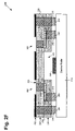
- conductive vias 210 and 212 and metal band 214 are formed in polymer layer 208 and passive components 216 and 218 are formed on polymer layer 208 .
- Conductive vias 210 and 212 are situated in and extend through polymer layer 208 and can comprise a conductive material, such as copper, gold, nickel, a solder material, such as a tin-based solder material, or other appropriate metal or metal alloy.
- Conductive vias 210 and 212 can be formed by patterning via openings on polymer layer 208 and extending the via openings through polymer layer 208 by utilizing a reactive ion etch (RIE) process, a wet etch process, or other appropriate etch process.
- RIE reactive ion etch
- An electroless plating process, an electro-plating process, a screen printing process, or other appropriate deposition process can then be used to fill the via openings with conductive material to form conductive vias 210 and 212 .
- Metal band 214 is situated in and extends through polymer layer 208 and forms a continuous metal loop that extends along the perimeter of polymer layer 208 .
- Metal band 214 can comprise copper, gold, nickel, a solder material, such as a tin-based solder material, or other appropriate metal or metal alloy.
- Metal band 214 can be formed by patterning and etching a trench in polymer layer 208 . An electroless plating process, an electro-plating process, or other appropriate deposition process can then be used to fill the trench with an appropriate metal or metal alloy to form metal band 214 .
- Passive component 216 is situated on polymer layer 208 and has terminal 220 , which is situated over and in electrical contact with conductive via 210 , and terminal 222 .
- Passive component 216 can be a resistor, an inductor, or a capacitor and can comprise a metal such as tungsten or other appropriate metallic material.
- Passive component 218 is situated on polymer layer 208 and has terminal 224 , which is situated over and in electrical contact with conductive via 212 , and terminal 226 .
- Passive component 218 can be a resistor, an inductor, or a capacitor and can comprise a metal such as tungsten or other appropriate metallic material.
- Passive components 216 and 218 can be formed by depositing a redistribution layer comprising tungsten or other appropriate metallic material over polymer layer 208 and appropriately patterning and etching the redistribution layer.
- the result of step 172 of flowchart 100 is illustrated by structure 272 in FIG. 2B .
- polymer layer 228 is formed over polymer layer 208 and passive components 216 and 218 and conductive vias 230 and 232 , opening 234 , and metal band 236 are formed in polymer layer 228 .
- Polymer layer 228 is situated over polymer layer 208 and passive components 216 and 218 and can comprise a photoimageable polymer, such as BCB, SU-8, or one of the polyimide family of chemical structures.
- polymer layer 228 may comprise a photoimageable epoxy.
- polymer layer 228 and polymer layer 208 can comprise the same material.
- polymer layer 228 and polymer layer 208 can comprise different materials.
- polymer layer 228 can have a thickness of between approximately 5.0 microns and approximately 70.0 microns.
- Polymer layer 228 can be formed over polymer layer 208 and passive components 216 and 218 by using a spin coating process, a spraying process, a screen printing process, or other appropriate process.
- Conductive vias 230 and 232 are situated in polymer layer 228 and over respective passive components 216 and 218 .
- Conductive via 230 is situated over and in electrical contact with terminal 222 of passive component 216 and conductive via 232 is situated over and in electrical contact with terminal 226 of passive components 218 .
- Conductive vias 230 and 232 are substantially similar in composition and formation to conductive vias 210 and 214 .
- Opening 234 is situated in polymer layer 228 between conductive vias 230 and 232 and can be formed by appropriately patterning and etching polymer layer 228 .
- Metal band 236 is situated in and extends through polymer layer 228 and is also situated on metal band 214 .
- Metal band 236 forms a continuous metal loop that extends along the perimeter of polymer layer 228 and is substantially similar in composition, thickness, and formation to metal band 214 in polymer layer 208 .
- Metal band 236 and metal band 214 form metal sealing ring 238 , which forms a continuous metal loop that is situated in extends polymer layer 208 and polymer layer 228 and surrounds conductive vias 210 , 212 , 230 , and 232 and passive components 216 and 218 .
- the result of step 174 of flowchart 100 is illustrated by structure 274 in FIG. 2C .
- solder pads 240 and 242 are formed on respective conductive vias 230 and 232 , solder ring 244 is formed on metal sealing ring 238 , and device wafer 246 is bonded to polymer layer 228 .
- Solder pads 240 and 242 are situated on respective conductive vias 230 and 232 in polymer layer 228 and can comprise a solder material such as tin-silver-copper, tin-silver, gold-tin, indium, or other appropriate solder material having a low-temperature melting point.
- Solder pads 240 and 242 can be formed on respective conductive vias 230 and 232 by using a plating process or other appropriate deposition process.
- Solder ring 244 is situated on metal sealing ring 238 and is substantially similar in composition, thickness, and formation to solder pads 240 and 242 .
- Device wafer 246 which can comprise silicon and/or silicon-germanium, GaAs, InP, InGaP, and/or other materials, is situated over polymer layer 228 and includes device 248 , device wafer contact pads 250 and 252 , and metal device wafer ring 254 .
- Device 248 which can comprise an IC, such as an RF IC, is situated on device wafer 246 and also situated over opening 234 , which forms a cavity for device 248 .
- device 248 can comprise a MEMS device, such as an RF MEMS device.
- Device wafer contact pads 250 and 252 are situated on device wafer 246 and are electrically connected to device 248 and also electrically connected to terminals 222 and 226 of passive components 216 and 218 , respectively.
- Metal device wafer ring 254 is situated on device wafer 246 and forms a continuous metal loop that extends along the perimeter of device wafer 246 and surrounds device wafer contact pads 250 and 252 and device 248 .
- Metal device wafer ring 254 can be connected to ground in device wafer 246 . In one embodiment, metal device wafer ring 254 may not be connected to ground in device wafer 246 .
- Device wafer contact pads 250 and 252 and metal device wafer ring 254 can comprise copper, aluminum, or other appropriate metal or metal alloy and can be formed on device wafer 246 in a manner known in the art. It is noted that although a device wafer including only one device and two device contact pads is specifically discussed herein to preserve brevity, the device wafer may include a large number of device contact pads and multiple devices. Device wafer 246 can be bonded to polymer layer 228 by using solder pads 240 and 242 to solder conductive vias 230 and 232 to device wafer contact pads 250 and 252 , respectively, and by using solder ring 244 to solder metal sealing ring 238 to device wafer metal ring 254 . The result of step 176 of flowchart 100 is illustrated by structure 276 in FIG. 2D .
- a thinning process is performed to achieve target thickness 256 of device wafer 246 and handle wafer 204 is removed from metal seed layer 206 .
- target thickness 256 of device wafer 246 can be between approximately 50.0 microns and approximately 300.0 microns.
- target thickness 256 of device wafer 246 can be achieved by removing a sufficient amount of material from device wafer 246 .
- the thinning process can comprise a grinding process, a chemical mechanical polishing (CMP) process, an etching process, or other appropriate material removal process.
- CMP chemical mechanical polishing
- sacrificial coating 202 can be decomposed in a heating process to release handle wafer 204 from metal seed layer 206 .
- sacrificial coating 202 may be decomposed by using UV light or a chemical solution.
- metal seed layer 206 is removed from polymer layer 208 , passivation layer 258 is formed on exposed surface 260 of polymer layer 208 , and openings 262 and 264 are formed passivation layer 258 to expose respective conductive vias 210 and 212 .
- Metal seed layer 206 (shown in FIGS. 2A through 2E ) can be removed by using a wet or a dry etch process to expose surface 260 of polymer layer 208 .
- Passivation layer 258 is situated on surface 260 of polymer layer 208 and can comprise silicon dioxide, silicon nitride, or other appropriate dielectric material.
- Passivation layer 258 can be formed on polymer layer 208 by using a CVD process, a plasma enhanced chemical vapor deposition (PECVD) process, or other appropriate low temperature deposition process. Passivation layer 258 can have a thickness less than approximately 1.0 micron. In one embodiment, passivation layer 258 can have a thickness of between a few tenths of a nanometer and a few hundred nanometers. Openings 262 and 264 are situated over and expose respective conductive vias 210 and 212 and can be formed by appropriately patterning and etching passivation layer 258 . Passivation layer 258 and metal sealing ring 238 provide a hermetic seal for the present invention's wafer level package.
- PECVD plasma enhanced chemical vapor deposition
- passivation layer 258 and/or metal sealing ring 238 may not be used.
- the result of step 180 of flowchart 100 is illustrated by structure 280 in FIG. 2F .
- polymer layer contact pads 265 and 266 are formed over respective conductive vias 210 and 212 and solder bumps 267 and 268 are formed on respective polymer layer contact pads 265 and 266 .
- Polymer layer contact pads 265 and 266 are situated on respective conductive vias 210 and 212 and can comprise a portion of an under bump metallization (UBM) layer, which can comprise nickel, copper, vanadium, or other appropriate metal or metal alloy.
- UBM under bump metallization
- Polymer layer contact pads 265 and 266 can be formed by depositing a UBM layer over conductive vias 210 and 212 and passivation layer 258 by using a PVD process or other appropriate deposition process and appropriately patterning and etching the UBM layer.
- Polymer layer contact pad 265 is electrically connected to terminal 220 of passive component 216 by conductive via 210 and polymer layer contact pad 266 is electrically connected to terminal 224 of passive component 218 by conductive via 212 .
- Solder bumps 267 and 268 are situated on respective polymer layer contact pads 265 and 266 and can comprise an appropriate solder material. Solder bumps 267 and 268 can provide electrical connectivity between polymer layer contact pads 265 and 266 and devices and components external to the present invention's wafer level package, which houses device 248 and passive components 216 and 218 . In one embodiment, wire bonds may be used in place of solder bumps 267 and 268 to provide electrical connectivity between polymer layer contact pads 265 and 266 and devices and components external to the present invention's wafer level package.
- the result of step 182 of flowchart 100 is illustrated by structure 282 in FIG. 2G .
- the present invention advantageously achieves a wafer level package that includes passive components that are situated between polymer layers, which are situated over a device wafer, where the passive components can be connected to device wafer contact pads and also connected to external components and devices by polymer layer contact pads.
- the present invention effectively integrates passive components with a device wafer in a wafer level package without undesirably increasing the package footprint.
- the present invention advantageous achieves a hermetically sealed wafer level package having reduced cost compared to a conventional hermetically sealed wafer level package that achieves a hermetic seal by bonding a cap wafer to a device wafer with a metallic bonding material.
Abstract
Description
Claims (16)
Priority Applications (8)
| Application Number | Priority Date | Filing Date | Title |
|---|---|---|---|
| US11/097,646 US7576426B2 (en) | 2005-04-01 | 2005-04-01 | Wafer level package including a device wafer integrated with a passive component |
| CN2006800080156A CN101496162B (en) | 2005-04-01 | 2006-03-10 | Wafer level package including a device wafer integrated with a passive component |
| PCT/US2006/008599 WO2006107507A2 (en) | 2005-04-01 | 2006-03-10 | Wafer level package including a device wafer integrated with a passive component |
| EP06737749.9A EP1864325B1 (en) | 2005-04-01 | 2006-03-10 | Wafer level package including a device wafer integrated with a passive component |
| CN201110412463.5A CN102386166B (en) | 2005-04-01 | 2006-03-10 | Wafer level package including a device wafer integrated with a passive component |
| KR1020077023631A KR100924902B1 (en) | 2005-04-01 | 2006-03-10 | Wafer level package including a device wafer integrated with a passive component |
| TW095109200A TWI315569B (en) | 2005-04-01 | 2006-03-17 | Wafer level package including a device wafer integrated with a passive component |
| US11/899,926 US7629201B2 (en) | 2005-04-01 | 2007-09-07 | Method for fabricating a wafer level package with device wafer and passive component integration |
Applications Claiming Priority (1)
| Application Number | Priority Date | Filing Date | Title |
|---|---|---|---|
| US11/097,646 US7576426B2 (en) | 2005-04-01 | 2005-04-01 | Wafer level package including a device wafer integrated with a passive component |
Related Child Applications (1)
| Application Number | Title | Priority Date | Filing Date |
|---|---|---|---|
| US11/899,926 Division US7629201B2 (en) | 2005-04-01 | 2007-09-07 | Method for fabricating a wafer level package with device wafer and passive component integration |
Publications (2)
| Publication Number | Publication Date |
|---|---|
| US20060220173A1 US20060220173A1 (en) | 2006-10-05 |
| US7576426B2 true US7576426B2 (en) | 2009-08-18 |
Family
ID=37069324
Family Applications (2)
| Application Number | Title | Priority Date | Filing Date |
|---|---|---|---|
| US11/097,646 Active 2025-12-12 US7576426B2 (en) | 2005-04-01 | 2005-04-01 | Wafer level package including a device wafer integrated with a passive component |
| US11/899,926 Active 2025-09-16 US7629201B2 (en) | 2005-04-01 | 2007-09-07 | Method for fabricating a wafer level package with device wafer and passive component integration |
Family Applications After (1)
| Application Number | Title | Priority Date | Filing Date |
|---|---|---|---|
| US11/899,926 Active 2025-09-16 US7629201B2 (en) | 2005-04-01 | 2007-09-07 | Method for fabricating a wafer level package with device wafer and passive component integration |
Country Status (6)
| Country | Link |
|---|---|
| US (2) | US7576426B2 (en) |
| EP (1) | EP1864325B1 (en) |
| KR (1) | KR100924902B1 (en) |
| CN (2) | CN102386166B (en) |
| TW (1) | TWI315569B (en) |
| WO (1) | WO2006107507A2 (en) |
Cited By (11)
| Publication number | Priority date | Publication date | Assignee | Title |
|---|---|---|---|---|
| US20100244161A1 (en) * | 2007-11-30 | 2010-09-30 | Skyworks Solutions, Inc. | Wafer level packaging using flip chip mounting |
| US20100283144A1 (en) * | 2007-12-26 | 2010-11-11 | Steve Xin Liang | In-situ cavity circuit package |
| US20110114355A1 (en) * | 2008-05-27 | 2011-05-19 | Epcos Ag | Hermetically sealed housing for electronic components and manufacturing method |
| US7955885B1 (en) | 2009-01-09 | 2011-06-07 | Integrated Device Technology, Inc. | Methods of forming packaged micro-electromechanical devices |
| US20110187005A1 (en) * | 2010-02-03 | 2011-08-04 | Stats Chippac, Ltd. | Semiconductor Device and Method of Forming Cavity Adjacent to Sensitive Region of Semiconductor Die Using Wafer-Level Underfill Material |
| DE102012112058A1 (en) * | 2012-12-11 | 2014-06-12 | Epcos Ag | MEMS device and method for encapsulating MEMS devices |
| US20150028360A1 (en) * | 2013-07-25 | 2015-01-29 | Lingsen Precision Industries, Ltd. | Package structure of optical module |
| US20160363609A1 (en) * | 2013-02-27 | 2016-12-15 | Texas Instruments Incorporated | Method of forming capacitive mems sensor devices |
| US20180358308A1 (en) * | 2017-06-08 | 2018-12-13 | Wisol Co., Ltd. | Wafer level package and manufacturing method thereof |
| US11316550B2 (en) | 2020-01-15 | 2022-04-26 | Skyworks Solutions, Inc. | Biasing of cascode power amplifiers for multiple power supply domains |
| US11450630B2 (en) | 2020-10-27 | 2022-09-20 | Cirrus Logic, Inc. | Coupling of integrated circuits (ICS) through a passivation-defined contact pad |
Families Citing this family (47)
| Publication number | Priority date | Publication date | Assignee | Title |
|---|---|---|---|---|
| DE10203397B4 (en) * | 2002-01-29 | 2007-04-19 | Siemens Ag | Chip-size package with integrated passive component |
| GB0330010D0 (en) * | 2003-12-24 | 2004-01-28 | Cavendish Kinetics Ltd | Method for containing a device and a corresponding device |
| US20060211233A1 (en) * | 2005-03-21 | 2006-09-21 | Skyworks Solutions, Inc. | Method for fabricating a wafer level package having through wafer vias for external package connectivity and related structure |
| US7576426B2 (en) * | 2005-04-01 | 2009-08-18 | Skyworks Solutions, Inc. | Wafer level package including a device wafer integrated with a passive component |
| JP4891994B2 (en) * | 2005-06-30 | 2012-03-07 | シーメンス アクチエンゲゼルシヤフト | Circuit carrier for protecting sensitive electronic device data module against unauthorized operation from outside, and method of detecting unauthorized access to electronic device data module using the same |
| CN101390210B (en) * | 2005-12-28 | 2010-07-28 | 联合材料公司 | Semiconductor element mounting substrate, semiconductor device using the same, and process for producing semiconductor element mounting substrate |
| US7635606B2 (en) * | 2006-08-02 | 2009-12-22 | Skyworks Solutions, Inc. | Wafer level package with cavities for active devices |
| US20080217708A1 (en) * | 2007-03-09 | 2008-09-11 | Skyworks Solutions, Inc. | Integrated passive cap in a system-in-package |
| US7968978B2 (en) * | 2007-06-14 | 2011-06-28 | Raytheon Company | Microwave integrated circuit package and method for forming such package |
| US20080308922A1 (en) * | 2007-06-14 | 2008-12-18 | Yiwen Zhang | Method for packaging semiconductors at a wafer level |
| KR100927418B1 (en) * | 2007-09-28 | 2009-11-19 | 삼성전기주식회사 | Wafer level package and manufacturing method thereof |
| DE102007060632A1 (en) * | 2007-12-17 | 2009-06-18 | Robert Bosch Gmbh | Method for producing a cap wafer for a sensor |
| US7989262B2 (en) * | 2008-02-22 | 2011-08-02 | Cavendish Kinetics, Ltd. | Method of sealing a cavity |
| KR100980810B1 (en) | 2008-03-26 | 2010-09-10 | 주식회사 제이엠엘 | Image Sensor Module Capable of Wafer Level-Chip Scale Package and Fabricating Method thereof |
| US7993950B2 (en) * | 2008-04-30 | 2011-08-09 | Cavendish Kinetics, Ltd. | System and method of encapsulation |
| US7863699B2 (en) * | 2008-05-21 | 2011-01-04 | Triquint Semiconductor, Inc. | Bonded wafer package module |
| US8035219B2 (en) * | 2008-07-18 | 2011-10-11 | Raytheon Company | Packaging semiconductors at wafer level |
| US8018821B2 (en) * | 2008-09-30 | 2011-09-13 | Intel Corporation | Protection layers for media protection during fabrication of probe memory device |
| JP4972633B2 (en) * | 2008-12-11 | 2012-07-11 | 日東電工株式会社 | Manufacturing method of semiconductor device |
| JP5300558B2 (en) * | 2009-03-27 | 2013-09-25 | 日東電工株式会社 | Manufacturing method of semiconductor device |
| KR101067133B1 (en) * | 2009-08-17 | 2011-09-22 | 삼성전기주식회사 | Wafer level package with cylindrical capacitor and method of manufacturing the same |
| SG179006A1 (en) * | 2009-09-25 | 2012-04-27 | Agency Science Tech & Res | A wafer level package and a method of forming a wafer level package |
| TWI420988B (en) * | 2009-10-14 | 2013-12-21 | Wintec Ind Inc | Apparatus and method for vertically-structured passive components |
| US8987830B2 (en) * | 2010-01-12 | 2015-03-24 | Marvell World Trade Ltd. | Attaching passive components to a semiconductor package |
| KR100976813B1 (en) | 2010-04-23 | 2010-08-20 | 옵토팩 주식회사 | Eectronic device package and method of manufacturing the same |
| US8969176B2 (en) | 2010-12-03 | 2015-03-03 | Raytheon Company | Laminated transferable interconnect for microelectronic package |
| US8535983B2 (en) * | 2011-06-02 | 2013-09-17 | Infineon Technologies Ag | Method of manufacturing a semiconductor device |
| US8987898B2 (en) * | 2011-06-06 | 2015-03-24 | International Rectifier Corporation | Semiconductor wafer with reduced thickness variation and method for fabricating same |
| TWI447889B (en) * | 2011-08-05 | 2014-08-01 | Chipmos Technologies Inc | Chip package structure |
| US8624359B2 (en) * | 2011-10-05 | 2014-01-07 | Taiwan Semiconductor Manufacturing Company, Ltd. | Wafer level chip scale package and method of manufacturing the same |
| DE102012206732A1 (en) * | 2012-04-24 | 2013-10-24 | Robert Bosch Gmbh | Method for producing a hybrid integrated component |
| US9556017B2 (en) * | 2013-06-25 | 2017-01-31 | Analog Devices, Inc. | Apparatus and method for preventing stiction of MEMS devices encapsulated by active circuitry |
| US9208938B2 (en) * | 2013-10-02 | 2015-12-08 | Globalfoundries Inc. | Inductor structure having embedded airgap |
| US9123626B1 (en) * | 2014-02-27 | 2015-09-01 | Texas Instruments Incorporated | Integrated passive flip chip package |
| JP6339229B2 (en) | 2014-12-03 | 2018-06-06 | インテル・コーポレーション | Method for making an electronic package |
| CN105347289A (en) * | 2015-10-09 | 2016-02-24 | 锐迪科微电子(上海)有限公司 | Enclosing structure suitable for chip scale package and manufacturing method thereof |
| TW201735286A (en) * | 2016-02-11 | 2017-10-01 | 天工方案公司 | Device packaging using a recyclable carrier substrate |
| CN105742195A (en) * | 2016-04-01 | 2016-07-06 | 江苏长电科技股份有限公司 | Manufacturing method for etching buried hole-type surface sound filter chip packaging structure |
| CN105810597B (en) * | 2016-04-01 | 2018-10-09 | 江苏长电科技股份有限公司 | The manufacturing method of round metal chip level buried via hole type surface sound filtering chip encapsulating structure |
| CN105762085B (en) * | 2016-04-01 | 2019-01-01 | 江苏长电科技股份有限公司 | Metal disk buried via hole type surface sound filtering chip encapsulating structure and manufacturing method |
| CN105870077A (en) * | 2016-04-01 | 2016-08-17 | 江苏长电科技股份有限公司 | Buried hole-type surface acoustic wave filter chip packaging structure and manufacturing method thereof |
| CN105742255B (en) * | 2016-04-01 | 2018-10-09 | 江苏长电科技股份有限公司 | Round metal chip level groove buried via hole type surface sound filtering chip encapsulating structure and method |
| US10453763B2 (en) | 2016-08-10 | 2019-10-22 | Skyworks Solutions, Inc. | Packaging structures with improved adhesion and strength |
| DE102017212796A1 (en) * | 2017-07-26 | 2019-01-31 | Robert Bosch Gmbh | Electrical assembly |
| US10472228B2 (en) * | 2017-08-17 | 2019-11-12 | Advanced Semiconductor Engineering, Inc. | MEMS device package and method for manufacturing the same |
| US10854533B2 (en) * | 2018-03-26 | 2020-12-01 | Advanced Semiconductor Engineering, Inc. | Semiconductor package and method for manufacturing the same |
| US11075173B2 (en) * | 2018-10-31 | 2021-07-27 | Taiwan Semiconductor Manufacturing Company, Ltd. | Semiconductor device and method of forming same |
Citations (40)
| Publication number | Priority date | Publication date | Assignee | Title |
|---|---|---|---|---|
| US5323051A (en) | 1991-12-16 | 1994-06-21 | Motorola, Inc. | Semiconductor wafer level package |
| US5448014A (en) * | 1993-01-27 | 1995-09-05 | Trw Inc. | Mass simultaneous sealing and electrical connection of electronic devices |
| US5757072A (en) * | 1994-12-19 | 1998-05-26 | Martin Marietta Corporation | Structure for protecting air bridges on semiconductor chips from damage |
| US6057597A (en) | 1997-12-15 | 2000-05-02 | Micron Technology, Inc. | Semiconductor package with pre-fabricated cover |
| US6214644B1 (en) | 2000-06-30 | 2001-04-10 | Amkor Technology, Inc. | Flip-chip micromachine package fabrication method |
| US6297072B1 (en) | 1998-04-17 | 2001-10-02 | Interuniversitair Micro-Elktronica Centrum (Imec Vzw) | Method of fabrication of a microstructure having an internal cavity |
| US6376280B1 (en) | 1999-07-23 | 2002-04-23 | Agilent Technologies, Inc. | Microcap wafer-level package |
| US6380616B1 (en) | 1998-01-15 | 2002-04-30 | Infineon Technologies Ag | Semiconductor component with a number of substrate layers and at least one semiconductor chip, and method of producing the semiconductor component |
| US6399426B1 (en) | 1998-07-21 | 2002-06-04 | Miguel Albert Capote | Semiconductor flip-chip package and method for the fabrication thereof |
| US6402970B1 (en) | 2000-08-22 | 2002-06-11 | Charles W. C. Lin | Method of making a support circuit for a semiconductor chip assembly |
| US6498114B1 (en) | 1999-04-09 | 2002-12-24 | E Ink Corporation | Method for forming a patterned semiconductor film |
| US6530515B1 (en) | 2000-09-26 | 2003-03-11 | Amkor Technology, Inc. | Micromachine stacked flip chip package fabrication method |
| US6566745B1 (en) * | 1999-03-29 | 2003-05-20 | Imec Vzw | Image sensor ball grid array package and the fabrication thereof |
| US20030155643A1 (en) | 2002-02-19 | 2003-08-21 | Freidhoff Carl B. | Thin film encapsulation of MEMS devices |
| US6630725B1 (en) | 2000-10-06 | 2003-10-07 | Motorola, Inc. | Electronic component and method of manufacture |
| JP2004072071A (en) | 2002-06-13 | 2004-03-04 | Hitachi Chem Co Ltd | Method of manufacturing multilayer wiring board, and multilayer wiring board |
| US20040063249A1 (en) | 2002-01-19 | 2004-04-01 | Megic Corporation | Thin film semiconductor package and method of fabrication |
| US20040077154A1 (en) | 2002-10-17 | 2004-04-22 | Ranganathan Nagarajan | Wafer-level package for micro-electro-mechanical systems |
| US6743991B1 (en) * | 2003-04-14 | 2004-06-01 | Agilent Technologies, Inc. | Polymeric liquid metal switch |
| US6743656B2 (en) | 1999-10-04 | 2004-06-01 | Texas Instruments Incorporated | MEMS wafer level package |
| US6767764B2 (en) * | 2001-03-15 | 2004-07-27 | General Electric Company | Microelectromechanical system device packaging method |
| US6777263B1 (en) | 2003-08-21 | 2004-08-17 | Agilent Technologies, Inc. | Film deposition to enhance sealing yield of microcap wafer-level package with vias |
| US6787897B2 (en) | 2001-12-20 | 2004-09-07 | Agilent Technologies, Inc. | Wafer-level package with silicon gasket |
| US6794739B2 (en) | 2001-02-28 | 2004-09-21 | Sony Corporation | Semiconductor device, process for production thereof, and electronic equipment |
| US6800508B2 (en) | 2000-04-25 | 2004-10-05 | Torex Semiconductor Ltd | Semiconductor device, its manufacturing method and electrodeposition frame |
| US20040259325A1 (en) | 2003-06-19 | 2004-12-23 | Qing Gan | Wafer level chip scale hermetic package |
| US6838309B1 (en) | 2002-03-13 | 2005-01-04 | Amkor Technology, Inc. | Flip-chip micromachine package using seal layer |
| US20050054133A1 (en) | 2003-09-08 | 2005-03-10 | Felton Lawrence E. | Wafer level capped sensor |
| US6953999B2 (en) | 2003-02-06 | 2005-10-11 | Kulicke And Soffa Investments, Inc. | High density chip level package for the packaging of integrated circuits and method to manufacture same |
| US7045868B2 (en) | 2003-07-31 | 2006-05-16 | Motorola, Inc. | Wafer-level sealed microdevice having trench isolation and methods for making the same |
| US7059048B2 (en) | 2002-06-07 | 2006-06-13 | Intel Corporation | Wafer-level underfill process making use of sacrificial contact pad protective material |
| US20060126313A1 (en) * | 2002-06-26 | 2006-06-15 | Rainer Steiner | Electronic component with a housing package |
| US20060194361A1 (en) * | 2003-06-30 | 2006-08-31 | John Heck | MEMS packaging using a non-silicon substrate for encapsulation and interconnection |
| US20060211233A1 (en) | 2005-03-21 | 2006-09-21 | Skyworks Solutions, Inc. | Method for fabricating a wafer level package having through wafer vias for external package connectivity and related structure |
| US7203394B2 (en) | 2003-07-15 | 2007-04-10 | Rosemount Aerospace Inc. | Micro mirror arrays and microstructures with solderable connection sites |
| US20070158787A1 (en) * | 2003-11-13 | 2007-07-12 | Rajen Chanchani | Heterogeneously integrated microsystem-on-a-chip |
| US7268436B2 (en) | 2003-03-10 | 2007-09-11 | Infineon Technologies Ag | Electronic device with cavity and a method for producing the same |
| US20070274058A1 (en) | 2004-04-16 | 2007-11-29 | Koninklijke Philips Electronic N.V. | Integrated Circuit, a Method and an Assembly for Manufacturing the Integrated Circuit, and a Mobile Phone Having the Integrated Circuit |
| US20080003761A1 (en) | 2005-04-01 | 2008-01-03 | Skyworks Solutions, Inc. | Method for fabricating a wafer level package with device wafer and passive component integration |
| US20080217708A1 (en) | 2007-03-09 | 2008-09-11 | Skyworks Solutions, Inc. | Integrated passive cap in a system-in-package |
Family Cites Families (35)
| Publication number | Priority date | Publication date | Assignee | Title |
|---|---|---|---|---|
| US5798557A (en) * | 1996-08-29 | 1998-08-25 | Harris Corporation | Lid wafer bond packaging and micromachining |
| JP2000114413A (en) * | 1998-09-29 | 2000-04-21 | Sony Corp | Semiconductor device, its manufacture, and method for mounting parts |
| US6303423B1 (en) * | 1998-12-21 | 2001-10-16 | Megic Corporation | Method for forming high performance system-on-chip using post passivation process |
| CA2381230A1 (en) | 1999-09-03 | 2001-03-15 | Uniax Corporation | Encapsulation of organic electronic devices |
| US6297551B1 (en) * | 1999-09-22 | 2001-10-02 | Agere Systems Guardian Corp. | Integrated circuit packages with improved EMI characteristics |
| US6750521B1 (en) * | 1999-10-22 | 2004-06-15 | Delphi Technologies, Inc. | Surface mount package for a micromachined device |
| JP3597754B2 (en) * | 2000-04-24 | 2004-12-08 | Necエレクトロニクス株式会社 | Semiconductor device and manufacturing method thereof |
| TW457657B (en) | 2000-07-14 | 2001-10-01 | Jou Jeng San | Wafer-level packaging of micro electromechanical elements and fabrication method thereof |
| US6358773B1 (en) * | 2000-12-27 | 2002-03-19 | Vincent Lin | Method of making substrate for use in forming image sensor package |
| KR100518616B1 (en) * | 2001-01-18 | 2005-10-04 | 노키아 코포레이션 | Filter devices and method for fabricating filter devices |
| US6525420B2 (en) * | 2001-01-30 | 2003-02-25 | Thermal Corp. | Semiconductor package with lid heat spreader |
| JP4055368B2 (en) * | 2001-02-27 | 2008-03-05 | 日本電気株式会社 | Secondary battery |
| US6926057B2 (en) * | 2001-09-25 | 2005-08-09 | Dainippon Screen Mfg. Co., Ltd. | Thin film forming apparatus and thin film forming method |
| TWI312166B (en) * | 2001-09-28 | 2009-07-11 | Toppan Printing Co Ltd | Multi-layer circuit board, integrated circuit package, and manufacturing method for multi-layer circuit board |
| TW560018B (en) * | 2001-10-30 | 2003-11-01 | Asia Pacific Microsystems Inc | A wafer level packaged structure and method for manufacturing the same |
| JP2003218256A (en) | 2002-01-21 | 2003-07-31 | Kyocera Corp | Package for accommodating electronic component |
| US6660564B2 (en) * | 2002-01-25 | 2003-12-09 | Sony Corporation | Wafer-level through-wafer packaging process for MEMS and MEMS package produced thereby |
| CN100446243C (en) * | 2002-03-19 | 2008-12-24 | Nxp股份有限公司 | Design of an insulated cavity |
| KR100850879B1 (en) | 2002-05-15 | 2008-08-07 | 엘지이노텍 주식회사 | Antenna switch using low temperature co-fired ceramic |
| SE0202681D0 (en) * | 2002-09-10 | 2002-09-10 | Frank Niklaus | Hermetic sealing with combined adhesive bonding and sealing rings |
| JP4342174B2 (en) * | 2002-12-27 | 2009-10-14 | 新光電気工業株式会社 | Electronic device and manufacturing method thereof |
| US6812558B2 (en) * | 2003-03-26 | 2004-11-02 | Northrop Grumman Corporation | Wafer scale package and method of assembly |
| JP4269806B2 (en) * | 2003-06-30 | 2009-05-27 | カシオ計算機株式会社 | Semiconductor device and manufacturing method thereof |
| US7275424B2 (en) * | 2003-09-08 | 2007-10-02 | Analog Devices, Inc. | Wafer level capped sensor |
| WO2005031863A1 (en) * | 2003-09-26 | 2005-04-07 | Tessera, Inc. | Structure and method of making capped chips having vertical interconnects |
| KR20050040589A (en) * | 2003-10-29 | 2005-05-03 | 삼성전기주식회사 | Painted circuit board having the waveguide and manufacturing method thereof |
| KR100604334B1 (en) * | 2003-11-25 | 2006-08-08 | (주)케이나인 | Flip Chip Bondig Method for Enhancing the Performance of Connection in Flip Chip Packaging Process |
| US20050139984A1 (en) * | 2003-12-19 | 2005-06-30 | Tessera, Inc. | Package element and packaged chip having severable electrically conductive ties |
| US7061099B2 (en) * | 2004-09-30 | 2006-06-13 | Intel Corporation | Microelectronic package having chamber sealed by material including one or more intermetallic compounds |
| US7198725B2 (en) * | 2004-11-05 | 2007-04-03 | Chi-Yen Shen | Method for making a surface acoustic wave device package |
| US7202560B2 (en) * | 2004-12-15 | 2007-04-10 | Avago Technologies Wireless Ip (Singapore) Pte. Ltd. | Wafer bonding of micro-electro mechanical systems to active circuitry |
| US7169649B2 (en) * | 2004-12-16 | 2007-01-30 | Palo Alto Research Center, Inc. | Wafer scale integration of electroplated 3D structures using successive lithography, electroplated sacrificial layers, and flip-chip bonding |
| JP2006237406A (en) | 2005-02-25 | 2006-09-07 | Toshiba Corp | Resin sealed electronic component |
| US7323675B2 (en) * | 2005-09-21 | 2008-01-29 | Sigurd Microelectronics Corp. | Packaging structure of a light-sensing device with a spacer wall |
| US7635606B2 (en) | 2006-08-02 | 2009-12-22 | Skyworks Solutions, Inc. | Wafer level package with cavities for active devices |
-
2005
- 2005-04-01 US US11/097,646 patent/US7576426B2/en active Active
-
2006
- 2006-03-10 KR KR1020077023631A patent/KR100924902B1/en active IP Right Grant
- 2006-03-10 CN CN201110412463.5A patent/CN102386166B/en active Active
- 2006-03-10 CN CN2006800080156A patent/CN101496162B/en active Active
- 2006-03-10 WO PCT/US2006/008599 patent/WO2006107507A2/en active Application Filing
- 2006-03-10 EP EP06737749.9A patent/EP1864325B1/en active Active
- 2006-03-17 TW TW095109200A patent/TWI315569B/en active
-
2007
- 2007-09-07 US US11/899,926 patent/US7629201B2/en active Active
Patent Citations (41)
| Publication number | Priority date | Publication date | Assignee | Title |
|---|---|---|---|---|
| US5323051A (en) | 1991-12-16 | 1994-06-21 | Motorola, Inc. | Semiconductor wafer level package |
| US5448014A (en) * | 1993-01-27 | 1995-09-05 | Trw Inc. | Mass simultaneous sealing and electrical connection of electronic devices |
| US5757072A (en) * | 1994-12-19 | 1998-05-26 | Martin Marietta Corporation | Structure for protecting air bridges on semiconductor chips from damage |
| US6057597A (en) | 1997-12-15 | 2000-05-02 | Micron Technology, Inc. | Semiconductor package with pre-fabricated cover |
| US6380616B1 (en) | 1998-01-15 | 2002-04-30 | Infineon Technologies Ag | Semiconductor component with a number of substrate layers and at least one semiconductor chip, and method of producing the semiconductor component |
| US6297072B1 (en) | 1998-04-17 | 2001-10-02 | Interuniversitair Micro-Elktronica Centrum (Imec Vzw) | Method of fabrication of a microstructure having an internal cavity |
| US6399426B1 (en) | 1998-07-21 | 2002-06-04 | Miguel Albert Capote | Semiconductor flip-chip package and method for the fabrication thereof |
| US6566745B1 (en) * | 1999-03-29 | 2003-05-20 | Imec Vzw | Image sensor ball grid array package and the fabrication thereof |
| US6498114B1 (en) | 1999-04-09 | 2002-12-24 | E Ink Corporation | Method for forming a patterned semiconductor film |
| US6376280B1 (en) | 1999-07-23 | 2002-04-23 | Agilent Technologies, Inc. | Microcap wafer-level package |
| US6743656B2 (en) | 1999-10-04 | 2004-06-01 | Texas Instruments Incorporated | MEMS wafer level package |
| US6800508B2 (en) | 2000-04-25 | 2004-10-05 | Torex Semiconductor Ltd | Semiconductor device, its manufacturing method and electrodeposition frame |
| US6214644B1 (en) | 2000-06-30 | 2001-04-10 | Amkor Technology, Inc. | Flip-chip micromachine package fabrication method |
| US6402970B1 (en) | 2000-08-22 | 2002-06-11 | Charles W. C. Lin | Method of making a support circuit for a semiconductor chip assembly |
| US6530515B1 (en) | 2000-09-26 | 2003-03-11 | Amkor Technology, Inc. | Micromachine stacked flip chip package fabrication method |
| US6630725B1 (en) | 2000-10-06 | 2003-10-07 | Motorola, Inc. | Electronic component and method of manufacture |
| US6794739B2 (en) | 2001-02-28 | 2004-09-21 | Sony Corporation | Semiconductor device, process for production thereof, and electronic equipment |
| US6767764B2 (en) * | 2001-03-15 | 2004-07-27 | General Electric Company | Microelectromechanical system device packaging method |
| US6787897B2 (en) | 2001-12-20 | 2004-09-07 | Agilent Technologies, Inc. | Wafer-level package with silicon gasket |
| US20040063249A1 (en) | 2002-01-19 | 2004-04-01 | Megic Corporation | Thin film semiconductor package and method of fabrication |
| US20030155643A1 (en) | 2002-02-19 | 2003-08-21 | Freidhoff Carl B. | Thin film encapsulation of MEMS devices |
| US6838309B1 (en) | 2002-03-13 | 2005-01-04 | Amkor Technology, Inc. | Flip-chip micromachine package using seal layer |
| US7059048B2 (en) | 2002-06-07 | 2006-06-13 | Intel Corporation | Wafer-level underfill process making use of sacrificial contact pad protective material |
| JP2004072071A (en) | 2002-06-13 | 2004-03-04 | Hitachi Chem Co Ltd | Method of manufacturing multilayer wiring board, and multilayer wiring board |
| US20060126313A1 (en) * | 2002-06-26 | 2006-06-15 | Rainer Steiner | Electronic component with a housing package |
| US20040077154A1 (en) | 2002-10-17 | 2004-04-22 | Ranganathan Nagarajan | Wafer-level package for micro-electro-mechanical systems |
| US6953999B2 (en) | 2003-02-06 | 2005-10-11 | Kulicke And Soffa Investments, Inc. | High density chip level package for the packaging of integrated circuits and method to manufacture same |
| US7268436B2 (en) | 2003-03-10 | 2007-09-11 | Infineon Technologies Ag | Electronic device with cavity and a method for producing the same |
| US6743991B1 (en) * | 2003-04-14 | 2004-06-01 | Agilent Technologies, Inc. | Polymeric liquid metal switch |
| US20040259325A1 (en) | 2003-06-19 | 2004-12-23 | Qing Gan | Wafer level chip scale hermetic package |
| US20060194361A1 (en) * | 2003-06-30 | 2006-08-31 | John Heck | MEMS packaging using a non-silicon substrate for encapsulation and interconnection |
| US7203394B2 (en) | 2003-07-15 | 2007-04-10 | Rosemount Aerospace Inc. | Micro mirror arrays and microstructures with solderable connection sites |
| US7045868B2 (en) | 2003-07-31 | 2006-05-16 | Motorola, Inc. | Wafer-level sealed microdevice having trench isolation and methods for making the same |
| US6777263B1 (en) | 2003-08-21 | 2004-08-17 | Agilent Technologies, Inc. | Film deposition to enhance sealing yield of microcap wafer-level package with vias |
| US20050054133A1 (en) | 2003-09-08 | 2005-03-10 | Felton Lawrence E. | Wafer level capped sensor |
| US20070158787A1 (en) * | 2003-11-13 | 2007-07-12 | Rajen Chanchani | Heterogeneously integrated microsystem-on-a-chip |
| US20070274058A1 (en) | 2004-04-16 | 2007-11-29 | Koninklijke Philips Electronic N.V. | Integrated Circuit, a Method and an Assembly for Manufacturing the Integrated Circuit, and a Mobile Phone Having the Integrated Circuit |
| US20060211233A1 (en) | 2005-03-21 | 2006-09-21 | Skyworks Solutions, Inc. | Method for fabricating a wafer level package having through wafer vias for external package connectivity and related structure |
| US20080064142A1 (en) | 2005-03-21 | 2008-03-13 | Skyworks Solutions, Inc. | Method for fabricating a wafer level package having through wafer vias for external package connectivity |
| US20080003761A1 (en) | 2005-04-01 | 2008-01-03 | Skyworks Solutions, Inc. | Method for fabricating a wafer level package with device wafer and passive component integration |
| US20080217708A1 (en) | 2007-03-09 | 2008-09-11 | Skyworks Solutions, Inc. | Integrated passive cap in a system-in-package |
Non-Patent Citations (3)
| Title |
|---|
| K. C. Eun et al., "Fully Embedded LTCC Spiral Inductors Incorporating Air Cavity for High Q-factor and SRF," IEEE Electronic Components and Technology Conference, vol. 1, Jun. 1-4, 2004, pp. 1101-1103. |
| M. Franosch, "Wafer-Level-Package for Bulk Acoustic Wave (BAW) Filters," IEEE Microwaves Symposium, vol. 2, Jun. 6-11, 2004, pp. 493-496. |
| Young Chul Lee et al., "Monolithic LTCC SiP Transmitter for 60GHz Wireless Communication Terminals," IEEE Microwaves Symposium, Jun. 17, 2005, pp. 1015-1018. |
Cited By (27)
| Publication number | Priority date | Publication date | Assignee | Title |
|---|---|---|---|---|
| US8809116B2 (en) | 2007-11-30 | 2014-08-19 | Skyworks Solutions, Inc. | Method for wafer level packaging of electronic devices |
| US20100244161A1 (en) * | 2007-11-30 | 2010-09-30 | Skyworks Solutions, Inc. | Wafer level packaging using flip chip mounting |
| US8324728B2 (en) | 2007-11-30 | 2012-12-04 | Skyworks Solutions, Inc. | Wafer level packaging using flip chip mounting |
| US20100283144A1 (en) * | 2007-12-26 | 2010-11-11 | Steve Xin Liang | In-situ cavity circuit package |
| US9153551B2 (en) | 2007-12-26 | 2015-10-06 | Skyworks Solutions, Inc. | Integrated circuit package including in-situ formed cavity |
| US8900931B2 (en) | 2007-12-26 | 2014-12-02 | Skyworks Solutions, Inc. | In-situ cavity integrated circuit package |
| US20110114355A1 (en) * | 2008-05-27 | 2011-05-19 | Epcos Ag | Hermetically sealed housing for electronic components and manufacturing method |
| US8759677B2 (en) * | 2008-05-27 | 2014-06-24 | Epcos Ag | Hermetically sealed housing for electronic components and manufacturing method |
| US7955885B1 (en) | 2009-01-09 | 2011-06-07 | Integrated Device Technology, Inc. | Methods of forming packaged micro-electromechanical devices |
| US20110187005A1 (en) * | 2010-02-03 | 2011-08-04 | Stats Chippac, Ltd. | Semiconductor Device and Method of Forming Cavity Adjacent to Sensitive Region of Semiconductor Die Using Wafer-Level Underfill Material |
| US8574960B2 (en) * | 2010-02-03 | 2013-11-05 | Stats Chippac, Ltd. | Semiconductor device and method of forming cavity adjacent to sensitive region of semiconductor die using wafer-level underfill material |
| US9679881B2 (en) | 2010-02-03 | 2017-06-13 | STATS ChipPAC Pte. Ltd. | Semiconductor device and method of forming cavity adjacent to sensitive region of semiconductor die using wafer-level underfill material |
| DE102012112058A1 (en) * | 2012-12-11 | 2014-06-12 | Epcos Ag | MEMS device and method for encapsulating MEMS devices |
| DE102012112058B4 (en) * | 2012-12-11 | 2020-02-27 | Snaptrack, Inc. | MEMS component and method for encapsulating MEMS components |
| US10164166B2 (en) | 2012-12-11 | 2018-12-25 | Snaptrack, Inc. | MEMS component and method for encapsulating MEMS components |
| US9853204B2 (en) | 2012-12-11 | 2017-12-26 | Snaptrack, Inc. | MEMS component and method for encapsulating MEMS components |
| US10107830B2 (en) * | 2013-02-27 | 2018-10-23 | Texas Instruments Incorporated | Method of forming capacitive MEMS sensor devices |
| US20160363609A1 (en) * | 2013-02-27 | 2016-12-15 | Texas Instruments Incorporated | Method of forming capacitive mems sensor devices |
| US9190398B2 (en) * | 2013-07-25 | 2015-11-17 | Lingsen Precision Industries, Ltd. | Method for packaging an optical module |
| US20150091024A1 (en) * | 2013-07-25 | 2015-04-02 | Lingsen Precision Industries, Ltd. | Package structure of optical module |
| US20150028360A1 (en) * | 2013-07-25 | 2015-01-29 | Lingsen Precision Industries, Ltd. | Package structure of optical module |
| US20180358308A1 (en) * | 2017-06-08 | 2018-12-13 | Wisol Co., Ltd. | Wafer level package and manufacturing method thereof |
| US10446506B2 (en) * | 2017-06-08 | 2019-10-15 | Wisol Co., Ltd. | Wafer level package and manufacturing method thereof |
| US11316550B2 (en) | 2020-01-15 | 2022-04-26 | Skyworks Solutions, Inc. | Biasing of cascode power amplifiers for multiple power supply domains |
| US11671136B2 (en) | 2020-01-15 | 2023-06-06 | Skyworks Solutions, Inc. | Biasing of cascode power amplifiers for multiple power supply domains |
| US11936416B2 (en) | 2020-01-15 | 2024-03-19 | Skyworks Solutions, Inc. | Biasing of cascode power amplifiers for multiple power supply domains |
| US11450630B2 (en) | 2020-10-27 | 2022-09-20 | Cirrus Logic, Inc. | Coupling of integrated circuits (ICS) through a passivation-defined contact pad |
Also Published As
| Publication number | Publication date |
|---|---|
| TW200735312A (en) | 2007-09-16 |
| CN101496162B (en) | 2012-01-25 |
| CN101496162A (en) | 2009-07-29 |
| WO2006107507A2 (en) | 2006-10-12 |
| WO2006107507A3 (en) | 2009-04-16 |
| KR20070112277A (en) | 2007-11-22 |
| US7629201B2 (en) | 2009-12-08 |
| CN102386166B (en) | 2015-04-01 |
| CN102386166A (en) | 2012-03-21 |
| TWI315569B (en) | 2009-10-01 |
| KR100924902B1 (en) | 2009-11-05 |
| US20060220173A1 (en) | 2006-10-05 |
| EP1864325A2 (en) | 2007-12-12 |
| EP1864325A4 (en) | 2010-04-14 |
| EP1864325B1 (en) | 2017-10-18 |
| US20080003761A1 (en) | 2008-01-03 |
Similar Documents
| Publication | Publication Date | Title |
|---|---|---|
| US7576426B2 (en) | Wafer level package including a device wafer integrated with a passive component | |
| US20060211233A1 (en) | Method for fabricating a wafer level package having through wafer vias for external package connectivity and related structure | |
| US9685372B2 (en) | Method of forming Cu pillar bump with non-metal sidewall spacer and metal top cap | |
| US10074553B2 (en) | Wafer level package integration and method | |
| US9029193B2 (en) | Semiconductor device and method of forming an interconnect structure for 3-D devices using encapsulant for structural support | |
| US7749814B2 (en) | Semiconductor device with integrated passive circuit and method of making the same using sacrificial substrate | |
| US8409970B2 (en) | Semiconductor device and method of making integrated passive devices | |
| US8072059B2 (en) | Semiconductor device and method of forming UBM fixed relative to interconnect structure for alignment of semiconductor die | |
| TWI567866B (en) | Semiconductor device and method of forming an interconnect structure with tsv using encapsulant for structural support | |
| TWI520267B (en) | Semiconductor device and method of forming ipd in fan-out wafer level chip scale package | |
| US8860195B2 (en) | Apparatus and method for increasing the quantity of discrete electronic components in an integrated circuit package | |
| US11735497B2 (en) | Integrated passive device and fabrication method using a last through-substrate via | |
| US20090212429A1 (en) | Semiconductor Device and Method of Supporting a Wafer During Backgrinding and Reflow of Solder Bumps | |
| US20170194239A1 (en) | A semiconductor package having an etched groove for an embedded device formed on bottom surface of a support substrate and a method for fabricating the same | |
| US11127705B2 (en) | Semiconductor structure and manufacturing method thereof | |
| CN117326522A (en) | Method for manufacturing semiconductor device |
Legal Events
| Date | Code | Title | Description |
|---|---|---|---|
| AS | Assignment |
Owner name: SKYWORKS SOLUTIONS, INC., CALIFORNIA Free format text: ASSIGNMENT OF ASSIGNORS INTEREST;ASSIGNORS:GAN, QING;WARREN, ROBERT W.;LOBIANCO, ANTHONY J.;AND OTHERS;REEL/FRAME:016449/0727 Effective date: 20050324 |
|
| STCF | Information on status: patent grant |
Free format text: PATENTED CASE |
|
| FPAY | Fee payment |
Year of fee payment: 4 |
|
| FPAY | Fee payment |
Year of fee payment: 8 |
|
| MAFP | Maintenance fee payment |
Free format text: PAYMENT OF MAINTENANCE FEE, 12TH YEAR, LARGE ENTITY (ORIGINAL EVENT CODE: M1553); ENTITY STATUS OF PATENT OWNER: LARGE ENTITY Year of fee payment: 12 |