US6657531B2 - Fuse circuit using capacitors as fuse elements - Google Patents
Fuse circuit using capacitors as fuse elements Download PDFInfo
- Publication number
- US6657531B2 US6657531B2 US10/026,230 US2623001A US6657531B2 US 6657531 B2 US6657531 B2 US 6657531B2 US 2623001 A US2623001 A US 2623001A US 6657531 B2 US6657531 B2 US 6657531B2
- Authority
- US
- United States
- Prior art keywords
- electrical fuse
- fuse element
- destructive
- state
- voltage
- Prior art date
- Legal status (The legal status is an assumption and is not a legal conclusion. Google has not performed a legal analysis and makes no representation as to the accuracy of the status listed.)
- Expired - Fee Related, expires
Links
Images


Classifications
-
- G—PHYSICS
- G11—INFORMATION STORAGE
- G11C—STATIC STORES
- G11C29/00—Checking stores for correct operation ; Subsequent repair; Testing stores during standby or offline operation
-
- G—PHYSICS
- G11—INFORMATION STORAGE
- G11C—STATIC STORES
- G11C17/00—Read-only memories programmable only once; Semi-permanent stores, e.g. manually-replaceable information cards
- G11C17/14—Read-only memories programmable only once; Semi-permanent stores, e.g. manually-replaceable information cards in which contents are determined by selectively establishing, breaking or modifying connecting links by permanently altering the state of coupling elements, e.g. PROM
- G11C17/18—Auxiliary circuits, e.g. for writing into memory
-
- H—ELECTRICITY
- H01—ELECTRIC ELEMENTS
- H01L—SEMICONDUCTOR DEVICES NOT COVERED BY CLASS H10
- H01L2924/00—Indexing scheme for arrangements or methods for connecting or disconnecting semiconductor or solid-state bodies as covered by H01L24/00
- H01L2924/0001—Technical content checked by a classifier
- H01L2924/0002—Not covered by any one of groups H01L24/00, H01L24/00 and H01L2224/00
Definitions
- This invention relates to a fuse circuit using capacitors as fuse elements and more particularly to a fuse circuit to attain a stable operation when a destructive/nondestructive state of the fuse element is read out.
- a fuse element is widely used as one means for changing the circuit configuration of a completed semiconductor device.
- the conventional fuse element is formed of a metal or polysilicon material and it is a general method of blowing out the fuse element by use of a laser device.
- a laser device In order to blow out the fuse element by applying laser light, it is necessary to set up a state in which the fuse element is exposed and it is impossible to blow out the fuse element after it is sealed in a package, for example.
- the electrical fuse element uses a capacitor or high-resistance polysilicon layer as the fuse element and high voltage is applied to or a large current is supplied to the fuse element directly from an input pin or from a control circuit inside the chip to destroy the fuse element.
- a fuse element such as a high-resistance polysilicon layer which is normally set in a conductive state and made nonconductive at the time of destruction is called an electrical fuse and a fuse element such as a capacitor which is normally set in a nonconductive state and made conductive at the time of destruction is called an anti fuse in some cases.
- an electrical fuse In a wide sense, both of the above fuse elements are called an electrical fuse in this specification.
- the fuse circuit in the conventional system described in the above document is difficult to obtain a sufficiently large read current which permits the operation of reading out a destructive/nondestructive state to be stably performed. This is because a read current which is caused to flow to determine the destructive/nondestructive state is as small as several tenths ⁇ A to several ⁇ A and varies to a large extent when the capacitor used as the fuse element is destroyed.
- a fuse circuit comprises electrical fuse elements which are commonly connected at one-side ends; a voltage generating section which is configured to selectively apply program voltage for destroying the electrical fuse element and read voltage for reading out destructive/nondestructive states of the electrical fuse elements to a common connection node of the one-side ends of the electrical fuse elements; and a readout section which is configured to read out the destructive/nondestructive states of the electrical fuse elements from the other ends of the electrical fuse elements when the read voltage is applied to the common connection node from the voltage generating section.
- FIG. 1 is a circuit diagram showing an example of the circuit configuration of an electrical fuse system using capacitors as electrical fuse elements, for illustrating a fuse circuit according to a first embodiment of this invention
- FIG. 2 is a cross sectional view for illustrating an example of the structure of the electrical fuse element (capacitor) in the circuit shown in FIG. 1;
- FIG. 3 is a circuit diagram showing an example of the circuit configuration of an electrical fuse system using capacitor as electrical fuse elements, for illustrating a fuse circuit according to a second embodiment of this invention
- FIG. 4A is a logic circuit diagram for illustrating a concrete example of the configuration of a fuse determination circuit in the circuit shown in FIG. 3;
- FIG. 4B is a circuit diagram showing a concrete example of the circuit configuration of FIG. 4A, for illustrating a concrete example of the configuration of the fuse determination circuit in the circuit shown in FIG. 3;
- FIG. 5 is a circuit diagram showing an example of the circuit configuration of an electrical fuse system using capacitors as electrical fuse elements, for illustrating a modification of the fuse circuit according to the second embodiment of this invention
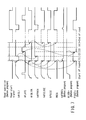
- FIG. 6 is a timing chart at the time of read operation (after program) in the circuit shown in FIGS. 3 to 5 ;
- FIG. 7 is a timing chart at the time of read operation (before program) in the circuit shown in FIGS. 3 to 5 .
- FIG. 1 is a circuit diagram showing an example of the circuit configuration of an electrical fuse system using capacitors as fuse elements, for illustrating a fuse circuit according to a first embodiment of this invention.
- the electrical fuse system includes a fuse address decoder 11 , fuse set 12 , program/read control circuit 18 , power supply conversion circuit 14 , verify output circuit 15 , read power supply circuit 19 and the like.
- the fuse address decoder 11 is supplied with a fuse address and a fuse selection signal ADDn output from the fuse address decoder 11 is supplied to the fuse set 12 .
- the fuse set 12 is configured to include a capacitor Q 1 as an electrical fuse element, NMOS (N-channel MOS) transistors Q 2 , Q 3 , Q 4 , fuse determination circuit 20 , fuse latch circuit 17 and the like.
- the fuse sets 12 corresponding in number (n) to fuse elements required are provided, but in FIG. 1, one fuse set is shown as a representative for brevity of the drawing. If n fuse sets are provided, one-side electrodes of capacitors Q 1 are commonly connected and the common connection node is connected to the program/ read control circuit 18 , power supply conversion circuit 14 , verify output circuit 15 and read power supply circuit 19 .
- One end of the current path of the NMOS transistor Q 3 is connected to the verify output circuit 15 , the other end of the current path thereof is connected to one-side ends of the NMOS transistors Q 2 , Q 4 and the gate thereof is supplied with the fuse selection signal ADDn output from the fuse address decoder 11 .
- the gate of the NMOS transistor Q 2 is supplied with a fuse determination circuit cut-off signal bAFCLOSE.
- the gate of the NMOS transistor Q 4 is connected to a power supply Vcc and the other end of the current path thereof is connected to one electrode of the capacitor Q 1 .
- the fuse determination circuit 20 is configured by an inverter 41 , NOR gate 42 and NAND gate 43 .
- the inverter 41 is supplied with the fuse determination circuit cut-off signal bAFCLOSE and an output signal from the inverter is supplied to one input terminal of the NOR gate 42 .
- the other input terminal of the NOR gate 42 is supplied with a signal AFUSEn output from the NAND gate 43 .
- One input terminal of the NAND gate 43 is supplied with a signal bAFPRCH which is an inverted signal of a precharge signal AFPRCH and the other input terminal thereof is supplied with a signal bAFUSEn output from the NOR gate 42 .
- a signal AFUSEn output from the NAND gate 43 is supplied to the fuse latch circuit 17 .
- the fuse latch circuit 17 is configured by a PMOS (P-channel MOS) transistor Q 7 and NMOS transistors Q 8 , Q 9 whose current paths are serially connected between the power supply Vcc and the ground node Vss and inverters 23 , 24 , 25 .
- the gate of the PMOS transistor Q 7 is supplied with the signal bAFPRCH which is an inverted signal of the precharge signal AFPRCH.
- the gate of the NMOS transistor Q 8 is supplied with a fuse latch signal AFLATCH.
- the gate of the NMOS transistor Q 9 is supplied with an output signal AFUSEn of the fuse determination circuit 16 .
- a connection node of the current paths of the PMOS transistor Q 7 and the NMOS transistor Q 8 is connected to the input terminal of the inverter 23 and the output terminal of the inverter 24 .
- the output terminal of the inverter 23 and the input terminal of the inverter 24 are connected to the input terminal of the inverter 25 .
- a signal FSOUTn is output from the output terminal of the inverter 25 .
- the program/read control circuit 18 is supplied with a program control signal and read control signal and supplies signals PULSE and bPULSE as a power supply conversion circuit control signal to the power supply conversion circuit 14 .
- a signal VERIFYcnt output from the program/read control circuit 18 is supplied to the verify output circuit 15 .
- the power supply conversion circuit 14 is operated on voltage between a power supply VBP and the ground node Vss to supply a stress signal PROG to the other electrode of the capacitor Q 1 used as the electrical fuse element.
- the verify output circuit 15 is configured by an inverter 30 and NMOS transistors Q 5 , Q 6 . One-side ends of the current paths of the NMOS transistors Q 5 and Q 6 are connected together and the other end of the NMOS transistor Q 6 is connected to the ground node Vss.
- the signal VERIFYcnt output from the program/read control circuit 18 is supplied to the gate of the NMOS transistor Q 6 and is inverted by the inverter 30 and supplied to the gate of the NMOS transistor Q 5 .
- a verify output is obtained from the other current path of the NMOS transistor Q 5 .
- the read power supply circuit 19 is configured by a PMOS transistor Q 20 and NMOS transistor Q 21 .
- One end of the current path of the PMOS transistor Q 20 is connected to the power supply Vcc and the gate thereof is supplied with a read control signal.
- One end of the current path of the NMOS transistor Q 21 is connected to the other end of the current path of the PMOS transistor Q 20 , the other end of the current path thereof is connected to the other electrode of the capacitor Q 1 and the gate thereof is connected to the power supply Vcc.
- FIG. 2 is a cross sectional view of a trench capacitor having the same structure as a trench type memory cell, for illustrating an example of the structure of the capacitor in the circuit shown in FIG. 1 .
- a buried plate 32 formed of a buried well region is formed in a deep position of a semiconductor substrate (silicon substrate) 31 and an element isolation region 33 of STI structure is formed in the surface region thereof.
- deep trenches 34 - 1 , 34 - 2 , . . . , 34 - n are formed to extend from the surface region to a depth so as to penetrate through the buried plate 32 .
- n-type diffused layers 37 - 1 , 37 - 2 , . . . , 37 - n are formed, respectively.
- an inter-level insulating film 38 is formed and metal interconnections 40 are formed on the inter-level insulating film 38 .
- contact plugs 39 - 1 , 39 - 2 , . . . , 39 - n are respectively formed and the buried electrodes 36 - 1 , 36 - 2 , . . . , 36 - n are electrically connected to the metal interconnections 40 - 1 , 40 - 2 , . . . , 40 - n via the n-type diffused layers 37 - 1 , 37 - 2 , . . . , 37 - n and contact plugs 39 - 1 , 39 - 2 , . . . , 39 - n , respectively.
- the buried plate 32 corresponds to one electrode of each of capacitors Q 1 - 1 , Q 1 - 2 , . . . , Q 1 - n used as fuse elements, each of the capacitor insulating films 35 corresponds to a capacitor insulating film, and the buried electrodes 36 - 1 , 36 - 2 , . . . , 36 - n respectively correspond to the other electrodes of the capacitors. That is, the buried plate 32 is commonly used by a plurality of capacitors Q 1 - 1 , Q 1 - 2 , . . . , Q 1 - n . Further, the metal interconnections 40 - 1 , 40 - 2 , . . . , 40 - n respectively correspond to interconnections connected to the other electrodes of the capacitors Q 1 - 1 , Q 1 - 2 , . . . , Q 1 - n.
- an electrical fuse element which is desired to be subjected to the program operation is selected by inputting an address of the fuse element Q 1 (Q 1 - 1 , Q 1 - 2 , . . . , Q 1 - n ) which is desired to be programmed to the fuse address decoder 11 and setting the fuse selection signal ADDn to the “H” level so as to turn ON the transistor Q 3 .
- the fuse determination circuit cut-off signal bAFCLOSE is set to the “L” level to turn OFF the transistor Q 2 so as to electrically isolate the fuse determination circuit 20 from the fuse element Q 1 .
- the program control signal is supplied to the program/read control circuit 18 so that the circuit 18 will turn ON the transistor Q 6 , thereby attaining a current path from VBP to Vss and setting a stress signal PROG to a VBP potential by use of the power supply conversion circuit control signals PULSE, bPULSE to apply stress to the fuse element Q 1 .
- the read power supply circuit 19 is prevented from being operated by setting the read control signal to the “H” level to turn OFF the transistor Q 20 .
- the verify (destruction determining) operation an address of the fuse element Q 1 which is desired to be verified is input to the fuse address decoder 11 to select the fuse element. Then, the program control signal is input, but in this case, the verify operation is different from the program operation in that the power supply conversion circuit control signals PULSE, bPULSE are input to the power supply conversion circuit 14 so as to set the stress signal PROG into an electrically floating state by use of the read control signal, and at the same time, the read power supply circuit 19 is operated to charge the stress signal PROG to the “H” level (in this case, (Vcc-VthN)).
- the circuit configuration is made to turn ON the transistor Q 5 by use of the read control signal and a current path is attained between the power supply Vcc of the read power supply circuit 19 and the verify output node.
- a current path is attained between the power supply Vcc of the read power supply circuit 19 and the verify output node.
- a DC current path is formed between the power supply Vcc and the verify output node via the transistor Q 5 if the fuse element Q 1 has been destroyed, it becomes possible to monitor a current by use of an external pad, for example.
- a pulse of “L” level is supplied as the precharge signal bAFPRCH supplied to the fuse determination circuit 20 at the start timing of the read operation, the signal AFUSEn is charged to the “H” level and the signal bAFUSEn is set to the “L” level and latched.
- the fuse selection signal ADDn is set at the “L” level and the fuse determination circuit cut-off signal bAFCLOSE is set at the “H” level.
- a signal FINT is also charged to the “H” level and latched.
- the signal bAFPRCH is set to the “H” level.
- the signal bAFUSEn is coupled to the signal PROG and set to the “H” level (in this case, (Vcc-VthN)) when the fuse element Q 1 is set in the destructive state. Therefore, the state of the fuse determination circuit 20 is inverted to set the signal AFUSEn to the “L” level.
- the signals bAFUSEn and AFUSEn are respectively kept at the “L” level and “H” level when the fuse element Q 1 is set in the nondestructive state. If a pulse of “H” level is applied as the signal AFLATCH after the state of the signal AFUSEn is determined, an output signal FSOUTn is set to the “H” level while the signal FINTn is kept at the “H” level when the fuse element Q 1 has been destroyed. On the other hand, if the fuse element Q 1 is not destroyed, the signal FINTn is inverted to the “L” level and the output signal FSOUTn is set to the “L” level.
- n-type or p-type impurity of low impurity concentration is doped into the well region.
- n-type or p-type impurity of high impurity concentration is doped to reduce the resistance component on the other electrode side with an insulating film disposed therebetween.
- the fuse element is destroyed by applying high voltage to one electrode and connecting the other electrode to the ground node Vss.
- the high voltage in order to apply the high voltage to the other electrode side opposite to the well region with the insulating film disposed therebetween, it is necessary to selectively set the high voltage node or separate the well regions of the respective fuse elements and selectively set the ground node Vss. In either case, a heavy penalty will be imposed on the circuit and pattern area.
- the circuit and pattern area can be reduced in size.
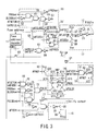
- FIGS. 3 to 5 show an example of the circuit configuration of an electrical fuse system using a capacitor as an electrical fuse element, for illustrating a fuse circuit according to a second embodiment of this invention.
- FIGS. 7 and 8 are timing charts in the read operation of the circuit shown in FIGS. 3 to 5 .
- FIGS. 3 to 5 constituent portions which are the similar to those of FIG. 1 are denoted by the same reference numerals and the detail explanation therefor is omitted.
- the circuit shown in FIG. 3 is different from the circuit shown in FIG. 1 in that a control circuit 50 of the fuse determination circuit and a read VBP circuit 80 are additionally provided, the logical configuration of a fuse determination circuit 20 ′ is changed because the control circuit 50 of the fuse determination circuit is additionally provided, the configuration of a read power supply circuit 19 ′ is changed and the concrete logical configuration of a program control circuit 18 ′ is changed.
- control circuit 50 of the fuse determination circuit is configured to include inverters 51 to 54 and NAND gates 55 to 57 .
- a program enable signal PROGen is supplied to the input terminal of the inverter 51 and one input terminal of the NAND gate 55 .
- An inverted signal bPROGen of the program enable signal PROGen output from the inverter 51 is supplied to the fuse determination circuit 20 ′.
- a program control circuit selection signal BLOCKsel is supplied to the other input terminal of the NAND gate 55 via the inverter 52 .
- An output signal of the NAND gate 55 is supplied to one input terminal of the NAND gate 56 .
- a read control signal AFSETOK is supplied to the other input terminal of the NAND gate 56 whose output signal is supplied to one input terminal of the NAND gate 57 .
- a fuse circuit interruption signal bAFKILL which is used to temporarily or permanently interrupt the operation of the fuse circuit is supplied to the other input terminal of the NAND gate 57 whose output signal is supplied to the input terminal of the inverter 53 .
- the inverter 53 supplies a fuse determination circuit cut-off signal bAFCLOSE to the gate of the transistor Q 2 and supplies the signal to the inverter 54 .
- An output signal AFCLOSE of the inverter 54 is supplied to the fuse determination circuit 20 ′.
- the fuse determination circuit 20 ′ is configured to include an OR gate 60 and NAND gates 61 , 62 .
- the signal AFCLOSE output from the inverter 54 is supplied to one input terminal of the OR gate 60 and a signal AFUSEn output from the NAND gate 62 is supplied to the other input terminal thereof.
- An output signal of the OR gate 60 is supplied to one input terminal of the NAND gate 61 and a signal bPROGen output from the inverter 51 is supplied to the other input terminal of the NAND gate 61 .
- An output signal bAFUSE output from the NAND gate 61 is supplied to one end of the current path of the transistor Q 2 and one input terminal of the NAND gate 62 .
- a signal bAFPRCH which is an inverted signal of the precharge signal AFPRCH is supplied to the other input terminal of the NAND gate 62 .
- the signal bAFPRCH is generated by use of the NAND gate 63 which is supplied with the signal bAFKILL and signal bAFSET and the inverter 64 which inverts an output signal of the NAND gate 63 .
- the program control circuit 18 ′ is configured to include NAND gates 70 to 74 and inverters 75 to 78 .
- a read control signal AFSETOK and an inverted signal bAFVERI of a verify control signal AFVERI are supplied to the NAND gate 70 which in turn supplies an output signal to one input terminal of the NAND gate 73 via the inverter 75 .
- a program enable signal PROGen and program control circuit selection signal BLOCKsel are supplied to the NAND gate 71 which in turn supplies an output signal to one input terminal of the NAND gate 72 and the first input terminal of the NAND gate 74 via the inverter 76 .
- a program pulse control signal PULSEcnt is supplied to the other input terminal of the NAND gate 72 and supplied to the second input terminal of the NAND gate 74 via the inverter 78 .
- the verify control signal AFVERI is supplied to the third input terminal of the NAND gate 74 and supplied to the inverter 79 which in turn supplies an inverted signal bAFVERI.
- a signal PULSE output from the NAND gate 73 and a signal bPULSE obtained by inverting the above signal by use of the inverter 77 are supplied to the power supply conversion circuit 14 as a power supply conversion circuit control signal. Further, an output signal of the NAND gate 74 is supplied to the verify output circuit 15 .
- the read VBP circuit 80 is configured by an NMOS transistor Q 30 having a current path which is connected at one end to the power supply Vcc and connected at the other end to a VBP node of the power supply conversion circuit 14 and a gate supplied with a power supply generation circuit control signal AFNGT.
- the program control circuit 18 ′ is configured to include a PMOS transistor Q 31 , NMOS transistor Q 32 , NAND gate 81 and inverter 82 .
- the NAND gate 81 is supplied with the inverted signal bAFVERI of the verify control signal AFVERI and a read control signal AFSETOK and supplies an output signal to the gate of the PMOS transistor Q 31 via the inverter 82 .
- One end of the current path of the PMOS transistor Q 31 is connected to the power supply Vcc and the other end of the current path thereof is connected to one end of the current path of the NMOS transistor Q 32 .
- the other end of the current path of the NMOS transistor Q 32 is connected to the other electrode of the capacitor Q 1 used as a fuse element and the gate thereof is supplied with the power supply generation circuit control signal AFNGT.
- FIGS. 4A and 4B specifically illustrate the fuse determination circuit 20 ′ shown in FIG. 3, FIG. 4A is a logical circuit diagram and FIG. 4B is a circuit diagram showing the detail circuit configuration thereof.
- the circuit is configured to include NMOS transistors Q 41 , Q 43 to Q 48 , Q 50 , Q 51 and PMOS transistors Q 42 , Q 45 , Q 46 , Q 49 , Q 52 .
- One end of the current path of the PMOS transistor Q 41 and the gate thereof are connected to the power supply Vcc.
- the current paths of the PMOS transistor Q 42 and NMOS transistors Q 43 , Q 44 are serially connected between the other end of the current path of the PMOS transistor Q 41 and the ground node Vss.
- the other end of the current path of the PMOS transistor Q 41 is connected to one end of the current path of the PMOS transistor Q 45 .
- the other end of the current path of the PMOS transistor Q 45 is connected to one end of the current path of the PMOS transistor Q 46 and the other end of the current path of the PMOS transistor Q 46 is connected to a connection node of the current paths of the PMOS transistor Q 42 and the NMOS transistor Q 43 .
- a connection node of the current paths of the NMOS transistors Q 43 and Q 44 is connected to one end of the current path of the NMOS transistor Q 47 which is connected to the ground node Vss at the other end of the current path.
- the gates of the PMOS transistor Q 42 and the NMOS transistor Q 43 are supplied with an inverted signal bPROGen of the program enable signal PROGen and the gates of the PMOS transistor Q 45 and the NMOS transistor Q 47 are supplied with a fuse determination circuit cut-off signal bAFCLOSE.
- a signal bAFUSEn is output from a connection node of the current paths of the PMOS transistors Q 42 , Q 46 and the NMOS transistor Q 43 .
- One end of the current path of the PMOS transistor Q 48 and the gate thereof are connected to the power supply Vcc.
- the current paths of the PMOS transistor Q 49 and NMOS transistors Q 50 , Q 51 are serially connected between the other end of the current path of the PMOS transistor Q 48 and the ground node Vss.
- the other end of the current path of the PMOS transistor Q 48 is connected to one end of the current path of the PMOS transistor Q 52 .
- the other end of the current path of the PMOS transistor Q 52 is connected to a connection node of the current paths of the PMOS transistor Q 49 and the NMOS transistor Q 50 .
- the gates of the PMOS transistor Q 49 and the NMOS transistor Q 50 are supplied with the signal bAFUSEn and the gates of the PMOS transistor Q 52 and the NMOS transistor Q 51 are supplied with a signal bAFPRCH which is an inverted signal of the precharge signal AFPRCH.
- a signal AFUSEn is output from a connection node of the current paths of the PMOS transistors Q 49 , Q 52 and the NMOS transistor Q 50 and supplied to the gates of the NMOS transistor Q 44 and PMOS transistor Q 46 .
- the reason why the NMOS transistors Q 41 , Q 48 are provided in the concrete example of the circuit of the fuse determination circuit 20 ′ of FIG. 4 B and the potential (Vcc-VthN) which is lowered by the threshold voltage of the NMOS transistor is used as the power supply voltage is as follows. That is, the signal bAFUSEn is charged to the “H” level when the fuse element Q 1 is set in the destructive state in the read operation, but at this time, the “H” level is set to a potential of (Vcc-VthN) because of the NMOS transistor Q 4 whose gate is applied with the power supply voltage Vcc.
- both of the PMOS transistor and NMOS transistor of the 2-input NAND logic circuit are turned ON so that the signal AFUSEn may be set to the “L” level (Vss) with delay and erroneous data will be latched in the initial state in which the signal bAFPRCH is changed from the “L” level (Vss) to the “H” level (Vcc) to invert the state of the fuse determination circuit 20 ′ by use of the “H” level (Vcc-VthN) of the signal bAFUSEn.
- FIG. 5 shows a modification of the circuit shown in FIGS. 4A and 4B.
- the circuit includes inverters 98 , 99 instead of the fuse latch circuit 17 and part of a control circuit 50 ′ of the fuse determination circuit is changed according to a change in the circuit.
- the other basic configuration is the same as the circuit shown in FIGS. 4A and 4B and is operated in substantially the same manner.
- control circuit 50 ′ of the fuse determination circuit is configured by inverters 91 to 94 and NAND gates 95 to 97 .
- a program enable signal PROGen is supplied to the input terminal of the inverter 91 and one input terminal of the NAND gate 95 .
- An inverted signal bPROGen of the program enable signal PROGen output from the inverter 91 is supplied to the fuse determination circuit 20 ′.
- a program control circuit selection signal BLOCKsel is supplied to the other input terminal of the NAND gate 95 .
- An output signal of the NAND gate 95 is supplied to one input terminal of the NAND gate 96 .
- the other input terminal of the NAND gate 96 is supplied with a fuse circuit interruption signal bAFKILL which is used to temporarily or permanently interrupt the operation of the fuse circuit.
- the fuse circuit interruption signal bAFKILL is supplied to the first input terminal of the NAND gate 97 and a read control signal AFSETOK is supplied to the second input terminal thereof.
- An output signal AFCLOSE of the NAN gate 96 is supplied to the fuse determination circuit 20 ′ and supplied to the third input terminal of the NAND gate 97 via the inverter 92 .
- An output signal of the NAND gate 97 is supplied to the gate of the NMOS transistor Q 2 as a fuse determination circuit cut-off signal bAFCLOSE via the inverter 94 .
- the program enable signal PROGen is set to the “H” level so as to make the electrical fuse system operable.
- the inverted signal bPROGen of the program enable signal PROGen is set to the “L” level
- the signal bAFUSEn is charged to the “H” level.
- the fuse determination circuit cut-off signal bAFCLOSE is changed from the “L” level to the “H” level
- the transistor Q 2 is turned ON to electrically connect the fuse determination circuit 20 ′ and fuse element Q 1 to each other.
- the voltage across each of the transistors Q 4 in all of the fuse sets 12 is charged to (Vcc-VthN).
- the reason why the voltage across each of the transistors Q 4 in all of the fuse sets 12 is charged to (Vcc-VthN) is that stress (potential difference) applied to the non-selected fuse element Q 3 in the program operation is alleviated to enhance the reliability and the characteristic because the stress signal PROG is commonly supplied to all of the fuse sets 12 .
- a desired fuse set which is desired to be subjected to the program operation is selected from a plurality of fuse sets 12 by inputting an address of the fuse element Q 1 (Q 1 - 1 , Q 1 - 2 , . . . , Q 1 - n ) which is desired to be programmed to the fuse address decoder 11 and setting the fuse selection signal ADDn to the “H” level to turn ON the transistor Q 3 .
- the signal BLOCKsel is set to the “H” level by use of a fuse set selection address which is used to select a plurality of fuse sets provided on the chip.
- the signal bAFCLOSE is set to the “L” level to turn OFF the transistor Q 2 so as to electrically isolate the fuse determination circuit 20 ′ of the selected fuse set from the fuse element Q 1 .
- stress is applied to the fuse element Q 1 by setting the program pulse control signal PULSEcnt to the “H” level to turn ON the transistor Q 6 so as to attain a current path from VBP to the ground node Vss and setting the power supply conversion circuit control signals PULSE and bPULSE to the “H” level and “L” level, respectively, to set the stress signal PROG to the VBP potential.
- the verify control signal AFVERI and read control signal AFSETOK are both set at the “L” level and an inverted signal bAFVERI of the verify control signal AFVERI is set at the “H” level, the read power supply circuit 19 ′ is not operated.
- a power supply generation circuit control signal AFNGT is kept at the Vcc level.
- the verify (destruction determining) operation is performed as follows. Like the program operation, an address of the fuse element Q 1 which is desired to be verified is input to the fuse address decoder 11 to select the fuse element.
- the verify operation is different from the program operation in that the VBP potential is set into an electrically floating state or set to the same potential as the stress signal PROG and the signal AFNGT is set to potential equal to or higher than (Vcc+VthN)). The potential is used as the read power supply voltage.
- the signals PROGen and BLOCKsel which are set to the “H” level, the signal PULSEcnt which is set to the “L” level and the verify control signal AFVERI which is set to the “H” level are input to the program control circuit 18 ′ to attain a current path between the signal PROG and the verify output. Further, if the signal AFVERI is set to the “H” level, the signals PULSE, bPULSE are respectively set to the “H” level and “L” level and an output of the power supply conversion circuit 14 is set into an electrically floating state, but the signal PROG is charged to the Vcc level by use of the read power supply circuit 19 ′. At this time, since a DC current path is formed between the power supply Vcc and the verify output node via the transistor Q 5 if the fuse element Q 1 is not destroyed, it becomes possible to monitor a current by use of an external pad, for example.
- the read VBP circuit 80 is a circuit which generates the same potential as the signal PROG when VBP is set in the electrically floating condition and prevents flow of a forward current of a PN junction occurring in the PMOS transistor in the power supply conversion circuit 14 when the VBP potential becomes lower than the signal PROG.
- the reason why the signal AFNGT is set to potential equal to or higher than (Vcc+VthN) is that a larger read current is attained by increasing the potential difference applied across the fuse element Q 1 after it has been destroyed.
- FIG. 6 is a timing chart after program and FIG. 7 is a timing chart before program.
- the VBP potential is set into an electrically floating state or set to the same potential as the signal PROG and the signal AFNGT is set to potential which is not lower than (Vcc+VthN)).
- the potential is used as the read power supply voltage.
- the signals PROGen, BLOCKsel, PULSEcnt, AFVERI and ADDn input to the program control circuit 18 ′ are set at the “L” level.
- a set signal bAFSET of the fuse determination circuit 20 ′ is set to the “L” level in synchronism with the read control signal and a precharge signal bAFPRCH of the fuse determination circuit 20 ′ is set to the “L” level.
- the signal AFUSEn is charged to the “H” level and the signal bAFUSEn is set to the “L” level and latched.
- the signal FINT is charged to the “H” level and latched.
- the signal POG is charged to the Vcc potential by use of the read power supply circuit 19 ′ to apply potential to the fuse element Q 1 by setting a read completion signal AFSETOK to the “L” level and the transistor Q 2 which is a transfer gate between the fuse element Q 1 and the fuse determination circuit 20 ′ is turned ON by setting the signal bAFCLOSE to the “H” level, thereby permitting a current to flow in the same direction as in the case of the program operation.
- the reason why the signal bAFCLOSE is set at the “H” level in the “L” level period of the signal bAFPRCH is as follows. That is, the read power supply circuit 19 ′ charges the signal PROG to the Vcc potential if the signal AFSETOK is set at the “L” level, but since the signal PROG and the transistor Q 4 are capacitively coupled to each other by use of the fuse element Q 1 in the fuse set which is not programmed, the potentials of both ends of the transistor Q 4 are set into an electrically floating state when the signal PROG is charged to the Vcc potential.
- the setting operation of the signals AFUSEn, bAFUSEn is terminated by setting the signal bAFSET to the “H” level and setting the signal bAFPRCH to the “H” level after the “L” level latching state of the signal bAFUSEn and the “H” level latching state of the signal FINT are determined. Then, the level of the signal bAFUSEn is detected by use of the fuse determination circuit 20 ′ to determine the level of the signal AFUSEn.
- the signal bAFUSEn is coupled with the signal PROG and set to the “H” level (in this case, Vcc) to invert the state of the fuse determination circuit 20 ′ and set the signal AFUSEn to the “L” level. If the fuse element Q 1 is set in the nondestructive state, the signal bAFUSEn is kept at the “L” level and the signal AFUSEn is kept at the “H” level (( 2 ) in FIGS. 6 and 7 ).
- the destructive/nondestructive state of the fuse element Q 1 is determined by use of the fuse determination circuit 20 ′, and after the levels of the signals AFUSEn, bAFUSEn are determined, the signal AFLATCH is set to the “H” level. If the signal AFUSEn is set at the “H” level (destructive state), the signal FINT is drawn to the “L” level and latched, if the signal AFUSEn is set at the “L” level (nondestructive state), the signal FINT is kept at the “H” level and latched, and the respective states are output from the fuse latch circuit 17 (in the period ( 3 ) in FIGS. 6 and 7 ).
- the signal AFSETOK is set to the “H” level to set the signal PROG to the Vss level and turn OFF the transistor Q 2 so as to terminate the read operation (in the period ( 4 ) in FIGS. 6 and 7 ).
- the read start signal may be generated in synchronism with the rise of the power supply voltage Vcc as in the conventional case, but it becomes possible to attain a lager read current of the fuse element Q 1 after destruction by making a configuration which outputs the read start signal after the power supply voltage Vcc is raised to a rated potential and becomes sufficiently stable.
- the internal power supply generation circuits of the semiconductor device are driven to operate the internal power supply circuits immediately after the power supply Vcc is turned ON. Then, when the internal circuit detects that the internal power supply voltages becomes a preset potential, it outputs a signal which permits the normal operation to be started and the respective internal circuits can be set into operable states in response to the above signal. That is, since the power supply voltage Vcc is sufficiently raised to a rated potential and becomes stable in this state, the read start signal is output in synchronism with the operation enable signal of the respective internal circuits.
- the read operation can be performed by use of the power supply voltage in the more stable state by generating a read start signal in synchronism with the reset signal. Further, since the fuse circuit is set each time a series of normal operations is started, it becomes possible to re-set the fuse circuit even when the fuse circuit causes an erroneous operation by the influence of noise or the like in the normal operation and the reliability of the operation of the fuse circuit can be enhanced.
- the fuse set 12 which detects the destructive/nondestructive state of the fuse element Q 1 is configured by the fuse determination circuit 20 ′ and fuse latch circuit 17 , but it becomes unnecessary to arrange the fuse latch circuit 17 by forming the control circuit 50 ′ of the fuse determination circuit to have a configuration as shown in the modification of FIG. 6 and the circuit configuration can be simplified.
- the inverters 98 , 99 are provided, but it is permitted to provide only one of them.
- the trench capacitor is used as the fuse element, but the same effect can be attained by using a capacitor of another structure such as a stack structure or MOS structure, for example. Further, it is possible to use an electrical fuse which is not a so-called anti fuse, and in this case, the polarity of the output FSOUTn is simply inverted and no problem occurs in the actual use.
- a fuse circuit can be obtained in which the stable operation can be attained in the read operation and verify operation and the reliability of the electrical fuse element can be enhanced.
Landscapes
- Design And Manufacture Of Integrated Circuits (AREA)
- Semiconductor Integrated Circuits (AREA)
- Read Only Memory (AREA)
- Fuses (AREA)
Applications Claiming Priority (2)
| Application Number | Priority Date | Filing Date | Title |
|---|---|---|---|
| JP2000-399222 | 2000-12-27 | ||
| JP2000399222A JP2002203901A (ja) | 2000-12-27 | 2000-12-27 | フューズ回路 |
Publications (2)
| Publication Number | Publication Date |
|---|---|
| US20020080004A1 US20020080004A1 (en) | 2002-06-27 |
| US6657531B2 true US6657531B2 (en) | 2003-12-02 |
Family
ID=18864036
Family Applications (1)
| Application Number | Title | Priority Date | Filing Date |
|---|---|---|---|
| US10/026,230 Expired - Fee Related US6657531B2 (en) | 2000-12-27 | 2001-12-21 | Fuse circuit using capacitors as fuse elements |
Country Status (7)
| Country | Link |
|---|---|
| US (1) | US6657531B2 (enExample) |
| EP (1) | EP1221699B1 (enExample) |
| JP (1) | JP2002203901A (enExample) |
| KR (1) | KR100458884B1 (enExample) |
| CN (1) | CN1362741A (enExample) |
| DE (1) | DE60129292T2 (enExample) |
| TW (1) | TW521392B (enExample) |
Cited By (5)
| Publication number | Priority date | Publication date | Assignee | Title |
|---|---|---|---|---|
| US20030049922A1 (en) * | 2001-09-13 | 2003-03-13 | Appel Andrew T. | Rectangular contact used as a low voltage fuse element |
| US20040150054A1 (en) * | 2003-01-29 | 2004-08-05 | Kawasaki Microelectronics, Inc. | Semiconductor integrated circuit including fuse device and method for manufacturing the same |
| US20080007986A1 (en) * | 2006-07-04 | 2008-01-10 | Samsung Electronics Co., Ltd. | One-time programmable devices including chalcogenide material, electronic systems including the same and methods of operating the same |
| US20120249221A1 (en) * | 2011-03-28 | 2012-10-04 | Hynix Semiconductor Inc. | Semiconductor integrated circuit |
| US8350264B2 (en) | 2010-07-14 | 2013-01-08 | International Businesss Machines Corporation | Secure anti-fuse with low voltage programming through localized diffusion heating |
Families Citing this family (10)
| Publication number | Priority date | Publication date | Assignee | Title |
|---|---|---|---|---|
| KR100448703B1 (ko) * | 2001-10-24 | 2004-09-16 | 삼성전자주식회사 | 메이크 링크 퓨즈를 구비한 회로 및 이를 이용한 반도체장치 |
| JP4179834B2 (ja) * | 2002-09-19 | 2008-11-12 | 株式会社リコー | 半導体装置の製造装置及び製造方法 |
| JP3878586B2 (ja) | 2003-07-17 | 2007-02-07 | 株式会社東芝 | リード/プログラム電位発生回路 |
| KR100528480B1 (ko) | 2003-12-09 | 2005-11-15 | 삼성전자주식회사 | 반도체장치의 전기적 퓨즈 회로 |
| JP5119626B2 (ja) * | 2006-08-18 | 2013-01-16 | 富士通セミコンダクター株式会社 | 電気ヒューズ回路 |
| CN103871475B (zh) * | 2014-02-21 | 2016-09-14 | 中国电子科技集团公司第二十四研究所 | 上电自复位的熔丝读取电路 |
| KR20150144147A (ko) * | 2014-06-16 | 2015-12-24 | 에스케이하이닉스 주식회사 | 반도체 장치 및 그의 동작방법 |
| CN117133342A (zh) * | 2022-05-19 | 2023-11-28 | 长鑫存储技术有限公司 | 反熔丝电路及反熔丝单元烧写状态验证方法 |
| CN117133341A (zh) * | 2022-05-19 | 2023-11-28 | 长鑫存储技术有限公司 | 反熔丝电路及反熔丝单元烧写状态实时验证方法 |
| US12389592B2 (en) * | 2022-07-04 | 2025-08-12 | Nanya Technology Corporation | Memory device and method of forming the same |
Citations (14)
| Publication number | Priority date | Publication date | Assignee | Title |
|---|---|---|---|---|
| US4730129A (en) * | 1984-02-29 | 1988-03-08 | Fujitsu Limited | Integrated circuit having fuse circuit |
| US5418487A (en) * | 1992-09-04 | 1995-05-23 | Benchmarg Microelectronics, Inc. | Fuse state sense circuit |
| US5442589A (en) * | 1992-10-29 | 1995-08-15 | Gemplus Card International | Fuse circuitry having physical fuse and non-volatile memory cell coupled to a detector |
| US5731733A (en) * | 1995-09-29 | 1998-03-24 | Intel Corporation | Static, low current sensing circuit for sensing the state of a fuse device |
| US6104649A (en) * | 1996-11-11 | 2000-08-15 | Kabushiki Kaisha Toshiba | Semiconductor memory device |
| US6172929B1 (en) * | 1999-06-25 | 2001-01-09 | Micron Technology, Inc. | Integrated circuit having aligned fuses and methods for forming and programming the fuses |
| JP2001067893A (ja) | 1999-08-27 | 2001-03-16 | Toshiba Corp | 電気フューズ素子を備えた半導体集積回路装置 |
| US6346846B1 (en) * | 1999-12-17 | 2002-02-12 | International Business Machines Corporation | Methods and apparatus for blowing and sensing antifuses |
| US6400632B1 (en) * | 2000-10-27 | 2002-06-04 | Mitsubishi Denki Kabushiki Kaisha | Semiconductor device including a fuse circuit in which the electric current is cut off after blowing so as to prevent voltage fall |
| US20020093867A1 (en) * | 2001-01-12 | 2002-07-18 | Kazuyoshi Muraoka | Semiconductor device having electric fuse element |
| US6426911B1 (en) * | 2000-10-19 | 2002-07-30 | Infineon Technologies Ag | Area efficient method for programming electrical fuses |
| US6430101B1 (en) * | 2000-08-17 | 2002-08-06 | Kabushiki Kaisha Toshiba | Fuse circuit using anti-fuse and method for searching for failed address in semiconductor memory |
| US6438059B2 (en) * | 2000-06-09 | 2002-08-20 | Kabushiki Kaisha Toshiba | Fuse programming circuit for programming fuses |
| US6498526B2 (en) * | 2000-03-23 | 2002-12-24 | Samsung Electronics Co., Ltd. | Fuse circuit and program status detecting method thereof |
Family Cites Families (9)
| Publication number | Priority date | Publication date | Assignee | Title |
|---|---|---|---|---|
| JPS60201598A (ja) * | 1984-03-23 | 1985-10-12 | Fujitsu Ltd | 半導体集積回路 |
| US5243226A (en) * | 1991-07-31 | 1993-09-07 | Quicklogic Corporation | Programming of antifuses |
| US5241496A (en) * | 1991-08-19 | 1993-08-31 | Micron Technology, Inc. | Array of read-only memory cells, eacch of which has a one-time, voltage-programmable antifuse element constructed within a trench shared by a pair of cells |
| US5444650A (en) * | 1994-01-25 | 1995-08-22 | Nippondenso Co., Ltd. | Semiconductor programmable read only memory device |
| US5635854A (en) * | 1994-05-24 | 1997-06-03 | Philips Electronics North America Corporation | Programmable logic integrated circuit including verify circuitry for classifying fuse link states as validly closed, validly open or invalid |
| KR970017759A (ko) * | 1995-09-14 | 1997-04-30 | 김광호 | 반도체 장치의 퓨즈용단 선택회로 |
| KR100228522B1 (ko) * | 1996-08-06 | 1999-11-01 | 윤종용 | 부분칩을 통한 전류 절감특성을 갖는 반도체메모리장치 |
| KR100250755B1 (ko) * | 1996-12-28 | 2000-05-01 | 김영환 | 플래쉬 메모리 장치 |
| JP3401522B2 (ja) * | 1998-07-06 | 2003-04-28 | 日本電気株式会社 | ヒューズ回路及び冗長デコーダ回路 |
-
2000
- 2000-12-27 JP JP2000399222A patent/JP2002203901A/ja active Pending
-
2001
- 2001-12-21 DE DE60129292T patent/DE60129292T2/de not_active Expired - Lifetime
- 2001-12-21 EP EP01130511A patent/EP1221699B1/en not_active Expired - Lifetime
- 2001-12-21 US US10/026,230 patent/US6657531B2/en not_active Expired - Fee Related
- 2001-12-26 TW TW090132334A patent/TW521392B/zh active
- 2001-12-27 KR KR10-2001-0085949A patent/KR100458884B1/ko not_active Expired - Fee Related
- 2001-12-27 CN CN01143949A patent/CN1362741A/zh active Pending
Patent Citations (14)
| Publication number | Priority date | Publication date | Assignee | Title |
|---|---|---|---|---|
| US4730129A (en) * | 1984-02-29 | 1988-03-08 | Fujitsu Limited | Integrated circuit having fuse circuit |
| US5418487A (en) * | 1992-09-04 | 1995-05-23 | Benchmarg Microelectronics, Inc. | Fuse state sense circuit |
| US5442589A (en) * | 1992-10-29 | 1995-08-15 | Gemplus Card International | Fuse circuitry having physical fuse and non-volatile memory cell coupled to a detector |
| US5731733A (en) * | 1995-09-29 | 1998-03-24 | Intel Corporation | Static, low current sensing circuit for sensing the state of a fuse device |
| US6104649A (en) * | 1996-11-11 | 2000-08-15 | Kabushiki Kaisha Toshiba | Semiconductor memory device |
| US6172929B1 (en) * | 1999-06-25 | 2001-01-09 | Micron Technology, Inc. | Integrated circuit having aligned fuses and methods for forming and programming the fuses |
| JP2001067893A (ja) | 1999-08-27 | 2001-03-16 | Toshiba Corp | 電気フューズ素子を備えた半導体集積回路装置 |
| US6346846B1 (en) * | 1999-12-17 | 2002-02-12 | International Business Machines Corporation | Methods and apparatus for blowing and sensing antifuses |
| US6498526B2 (en) * | 2000-03-23 | 2002-12-24 | Samsung Electronics Co., Ltd. | Fuse circuit and program status detecting method thereof |
| US6438059B2 (en) * | 2000-06-09 | 2002-08-20 | Kabushiki Kaisha Toshiba | Fuse programming circuit for programming fuses |
| US6430101B1 (en) * | 2000-08-17 | 2002-08-06 | Kabushiki Kaisha Toshiba | Fuse circuit using anti-fuse and method for searching for failed address in semiconductor memory |
| US6426911B1 (en) * | 2000-10-19 | 2002-07-30 | Infineon Technologies Ag | Area efficient method for programming electrical fuses |
| US6400632B1 (en) * | 2000-10-27 | 2002-06-04 | Mitsubishi Denki Kabushiki Kaisha | Semiconductor device including a fuse circuit in which the electric current is cut off after blowing so as to prevent voltage fall |
| US20020093867A1 (en) * | 2001-01-12 | 2002-07-18 | Kazuyoshi Muraoka | Semiconductor device having electric fuse element |
Cited By (15)
| Publication number | Priority date | Publication date | Assignee | Title |
|---|---|---|---|---|
| US20090017609A1 (en) * | 2001-09-13 | 2009-01-15 | Texas Instruments Incorporated | Rectangular contact used as a low voltage fuse element |
| US7977230B2 (en) | 2001-09-13 | 2011-07-12 | Texas Instruments Incorporated | Rectangular contact used as a low voltage fuse element |
| US6774457B2 (en) * | 2001-09-13 | 2004-08-10 | Texas Instruments Incorporated | Rectangular contact used as a low voltage fuse element |
| US20040227612A1 (en) * | 2001-09-13 | 2004-11-18 | Appel Andrew T. | Rectangular contact used as a low voltage fuse element |
| US20030049922A1 (en) * | 2001-09-13 | 2003-03-13 | Appel Andrew T. | Rectangular contact used as a low voltage fuse element |
| US7442626B2 (en) | 2001-09-13 | 2008-10-28 | Texas Instruments Incorporated | Rectangular contact used as a low voltage fuse element |
| US20040150054A1 (en) * | 2003-01-29 | 2004-08-05 | Kawasaki Microelectronics, Inc. | Semiconductor integrated circuit including fuse device and method for manufacturing the same |
| US20080007986A1 (en) * | 2006-07-04 | 2008-01-10 | Samsung Electronics Co., Ltd. | One-time programmable devices including chalcogenide material, electronic systems including the same and methods of operating the same |
| US20100090213A1 (en) * | 2006-07-04 | 2010-04-15 | Samsung Electronics Co., Ltd. | One-time programmable devices including chalcogenide material and electronic systems including the same |
| US7974115B2 (en) | 2006-07-04 | 2011-07-05 | Samsung Electronics Co., Ltd. | One-time programmable devices including chalcogenide material and electronic systems including the same |
| US7656694B2 (en) * | 2006-07-04 | 2010-02-02 | Samsung Electronics Co., Ltd. | Methods of programming one-time programmable devices including chalcogenide material |
| US8350264B2 (en) | 2010-07-14 | 2013-01-08 | International Businesss Machines Corporation | Secure anti-fuse with low voltage programming through localized diffusion heating |
| US8569755B2 (en) | 2010-07-14 | 2013-10-29 | International Business Machines Corporation | Secure anti-fuse with low voltage programming through localized diffusion heating |
| US20120249221A1 (en) * | 2011-03-28 | 2012-10-04 | Hynix Semiconductor Inc. | Semiconductor integrated circuit |
| US8598943B2 (en) * | 2011-03-28 | 2013-12-03 | SK Hynix Inc. | Semiconductor integrated circuit with stable rupture voltage fuse |
Also Published As
| Publication number | Publication date |
|---|---|
| EP1221699A3 (en) | 2004-11-17 |
| EP1221699A2 (en) | 2002-07-10 |
| KR20020053769A (ko) | 2002-07-05 |
| US20020080004A1 (en) | 2002-06-27 |
| DE60129292T2 (de) | 2008-03-20 |
| JP2002203901A (ja) | 2002-07-19 |
| DE60129292D1 (de) | 2007-08-23 |
| CN1362741A (zh) | 2002-08-07 |
| TW521392B (en) | 2003-02-21 |
| KR100458884B1 (ko) | 2004-12-03 |
| EP1221699B1 (en) | 2007-07-11 |
Similar Documents
| Publication | Publication Date | Title |
|---|---|---|
| US6421293B1 (en) | One-time programmable memory cell in CMOS technology | |
| US6657531B2 (en) | Fuse circuit using capacitors as fuse elements | |
| EP2195811B1 (en) | Anti-fuse element | |
| JP5536857B2 (ja) | 高速otp感知スキーム | |
| JP4531901B2 (ja) | ポストパッケージdramリペアのためのアンチヒューズ回路 | |
| US6420217B1 (en) | Method of an apparatus for programming an integrated fuse element to high resistance in low voltage technology | |
| US6909635B2 (en) | Programmable memory cell using charge trapping in a gate oxide | |
| US6721197B1 (en) | Antifuse memory cell and antifuse memory cell array | |
| US6400632B1 (en) | Semiconductor device including a fuse circuit in which the electric current is cut off after blowing so as to prevent voltage fall | |
| US6700166B2 (en) | Semiconductor memory device with improved soft-error resistance | |
| KR890001847B1 (ko) | 반도체 메모리 장치의 리던던시 회로 | |
| KR0153847B1 (ko) | 반도체 기억장치 | |
| JP3848022B2 (ja) | 電気フューズ素子を備えた半導体集積回路装置 | |
| US5361229A (en) | Precharging bitlines for robust reading of latch data | |
| US6327178B1 (en) | Programmable circuit and its method of operation | |
| EP0212946B1 (en) | Semiconductor memory device | |
| US6724676B1 (en) | Soft error improvement for latches | |
| JP2783398B2 (ja) | それぞれアンチ・ヒューズ素子を通じて基準電圧線に接続されたメモリー・セルigfetを有するワン・タイム電圧プログラマブル・リード・オンリー・メモリー・アレイ | |
| KR100498209B1 (ko) | 표면정렬셀 메모리를 갖는 반도체장치 | |
| JPH04358400A (ja) | 半導体記憶装置の冗長回路 | |
| KR19980013939A (ko) | 풀 씨모오스 스태틱 램 셀의 레이아웃 | |
| JPH0427638B2 (enExample) |
Legal Events
| Date | Code | Title | Description |
|---|---|---|---|
| AS | Assignment |
Owner name: KABUSHIKI KAISHA TOSHIBA, JAPAN Free format text: ASSIGNMENT OF ASSIGNORS INTEREST;ASSIGNORS:KIMURA, TOHRU;KOYANAGI, MASARU;REEL/FRAME:012397/0785 Effective date: 20011214 |
|
| FPAY | Fee payment |
Year of fee payment: 4 |
|
| REMI | Maintenance fee reminder mailed | ||
| LAPS | Lapse for failure to pay maintenance fees | ||
| STCH | Information on status: patent discontinuation |
Free format text: PATENT EXPIRED DUE TO NONPAYMENT OF MAINTENANCE FEES UNDER 37 CFR 1.362 |
|
| FP | Lapsed due to failure to pay maintenance fee |
Effective date: 20111202 |