US20120249221A1 - Semiconductor integrated circuit - Google Patents
Semiconductor integrated circuit Download PDFInfo
- Publication number
- US20120249221A1 US20120249221A1 US13/219,636 US201113219636A US2012249221A1 US 20120249221 A1 US20120249221 A1 US 20120249221A1 US 201113219636 A US201113219636 A US 201113219636A US 2012249221 A1 US2012249221 A1 US 2012249221A1
- Authority
- US
- United States
- Prior art keywords
- test mode
- signal
- integrated circuit
- semiconductor integrated
- fuse
- Prior art date
- Legal status (The legal status is an assumption and is not a legal conclusion. Google has not performed a legal analysis and makes no representation as to the accuracy of the status listed.)
- Granted
Links
Images


Classifications
-
- G—PHYSICS
- G11—INFORMATION STORAGE
- G11C—STATIC STORES
- G11C17/00—Read-only memories programmable only once; Semi-permanent stores, e.g. manually-replaceable information cards
- G11C17/14—Read-only memories programmable only once; Semi-permanent stores, e.g. manually-replaceable information cards in which contents are determined by selectively establishing, breaking or modifying connecting links by permanently altering the state of coupling elements, e.g. PROM
- G11C17/16—Read-only memories programmable only once; Semi-permanent stores, e.g. manually-replaceable information cards in which contents are determined by selectively establishing, breaking or modifying connecting links by permanently altering the state of coupling elements, e.g. PROM using electrically-fusible links
-
- G—PHYSICS
- G11—INFORMATION STORAGE
- G11C—STATIC STORES
- G11C29/00—Checking stores for correct operation ; Subsequent repair; Testing stores during standby or offline operation
- G11C29/04—Detection or location of defective memory elements, e.g. cell constructio details, timing of test signals
-
- G—PHYSICS
- G11—INFORMATION STORAGE
- G11C—STATIC STORES
- G11C29/00—Checking stores for correct operation ; Subsequent repair; Testing stores during standby or offline operation
- G11C29/70—Masking faults in memories by using spares or by reconfiguring
- G11C29/78—Masking faults in memories by using spares or by reconfiguring using programmable devices
- G11C29/785—Masking faults in memories by using spares or by reconfiguring using programmable devices with redundancy programming schemes
Definitions
- the present invention relates generally to a semiconductor circuit, and more particularly, to a semiconductor integrated circuit.
- a semiconductor integrated circuit employs fuses is which are used to change various setting values, perform repair operations, and so on.
- a fuse used in a semiconductor integrated circuit may be a laser fuse which is cut using a laser.
- the fuse used in the semiconductor integrated circuit may be an electronic fuse of which an electrical characteristics is changed by applying a high voltage.
- an electronic fuse includes an anti-fuse.
- the anti-fuse starts with a high resistance and is designed to create an electrically conductive path.
- rupture bias voltages are applied to a source, a drain and a gate commonly connected with one another to rupture a gate oxide Gox so that the gate, the source, the drain and a bulk are connected with one another.
- the electronic fuse may be used, e.g., may be electrically cut or connected even after packaging.
- a circuit for generating the rupture bias voltages may be included in the semiconductor integrated circuit, e.g., in a circuit configuration in which the electronic fuse is formed, or the rupture bias voltages may be provided from an external equipment.
- a known semiconductor integrated circuit 1 is configured to generate rupture bias voltages therein.
- the semiconductor integrated circuit 1 includes power supply control blocks 12 and 13 and a fuse set 11 .
- the fuse set 11 may be provided in a plural number, and each fuse set 11 may include a plurality of electronic fuses.
- the power supply control blocks 12 and 13 generate rupture bias voltages VPPF and VBBF using internal power sources VPP and VBB, respectively.
- the internal power sources VPP and VBB are power sources which are internally generated by a VPP pump (not shown) and a VBB pump (not shown), respectively.
- a known semiconductor integrated circuit 2 is configured to receive rupture bias voltages VPPF and VBBF from an external test equipment.
- the semiconductor integrated circuit 2 includes dedicated terminals 16 and 17 for rupture biases, power supply control blocks 14 and 15 , and a fuse set 11 .
- the dedicated terminals 16 and 17 for rupture biases are configured not to be used in a normal operation but to receive the rupture bias voltages VPPF and VBBF from the external test equipment only in a fuse rupture operation.
- the dedicated terminals 16 and 17 for rupture biases may be package balls of an FBGA (fine ball grid array) or pads.
- the power supply control blocks 14 and 15 provide the rupture bias voltages VPPF and VBBF supplied through the dedicated terminals 16 and 17 for rupture biases, to the fuse set 11 .
- a semiconductor integrated circuit which can supply stable rupture bias voltages and reduce the area of and improve the design efficiency of a circuit associated with power supply terminals is described herein.
- a semiconductor integrated circuit includes: a fuse set; a terminal assigned to be applied with a first external signal in a normal operation; and a control unit configured to receive a second external signal through the terminal and apply the received second external signal to the fuse set in a fuse control operation.
- a semiconductor integrated circuit includes: a fuse set; a first terminal assigned to be applied with a first external signal in a normal operation; a first control unit configured to receive a second external signal through the first terminal and apply the received second external signal to the fuse set in a fuse rupture operation; a second terminal assigned to be applied with a third external signal in the normal operation; and a second control unit configured to receive a fourth external signal through the second terminal and apply the received fourth external signal to the fuse set in the fuse rupture operation.
- FIG. 1 is a cross-sectional view illustrating a known electronic fuse
- FIG. 2 is a block diagram showing a known semiconductor integrated circuit
- FIG. 3 is a block diagram showing another known semiconductor integrated circuit
- FIG. 4 is a block diagram showing a semiconductor integrated circuit in accordance with an embodiment of the present invention.
- FIGS. 5 to 7 are circuit diagrams of exemplary embodiments of the semiconductor integrated circuit shown in FIG. 4 ;
- FIG. 8 is a block diagram showing a semiconductor integrated circuit in accordance with an embodiment of the present invention.
- FIG. 9 is a circuit diagram of the semiconductor integrated circuit shown in FIG. 8 ;
- FIG. 10 is a block diagram showing a semiconductor integrated circuit in accordance with an embodiment of the present invention.
- FIG. 11 is a circuit diagram of the semiconductor integrated circuit shown in FIG. 10 .
- dedicated terminals for rupture bias voltages are not used, and instead, through terminals assigned for a normal operation, first external signals are received in a normal operation and second external signals are received in a fuse control operation, e.g., a fuse rupture operation, to be applied to a selected fuse.
- a fuse control operation e.g., a fuse rupture operation
- Embodiments of the present invention exemplify the case of using terminals which are assigned for a normal operation and are not used in a test operation, and in particular, exemplify the case of using terminals which receive reference voltages as the first external is signals.
- Embodiments of the present invention exemplify the case in which rupture bias voltages are supplied as second external signals.
- the reference voltages may be used for determining the respective values of data and an address inputted to a semiconductor integrated circuit.
- FIG. 4 is a block diagram showing a semiconductor integrated circuit in accordance with an embodiment of the present invention.
- a semiconductor integrated circuit 100 in accordance with an embodiment of the present invention includes first and second terminals 130 and 140 , a control unit 200 , and a fuse set 500 .
- the first terminal 130 receives a voltage from a controller which is electrically connected with the semiconductor integrated circuit 100 in a normal operation.
- the controller may provide a first reference voltage VREF_DQ with a preset level (for example, VDD/2) to the first terminal 130 .
- the first terminal 130 may be provided with a voltage from a test equipment in a fuse rupture operation.
- the test equipment may provide a first rupture bias voltage VRUPTP which has a different level from a voltage level of an operation voltage in the normal operation, e.g., the same level as the rupture bias voltage VPPF described above with reference to FIG. 3 , to the first terminal 130 .
- the second terminal 140 receives a voltage from the controller which is electrically connected with the semiconductor integrated circuit 100 in the normal operation.
- the controller may provide a second reference voltage VREF_CA with a preset level (for example, VDD/2) to the second terminal 140 .
- the second terminal 140 may be provided with a voltage from the test equipment in the fuse rupture operation.
- the test equipment may provide a second rupture bias voltage VRUPTB which has a different level from a voltage level of an operation voltage in the normal operation, e.g., the same level as the rupture bias voltage VBBF described above with reference to FIG. 3 , to the second terminal 140 .
- the control unit 200 is configured to couple the first and second terminals 130 and 140 to the fuse set 500 in response to a test mode signal TM.
- control unit 200 electrically connects the first and second terminals 130 and 140 with the fuse set 500 in response to activation of the test mode signal TM.
- control unit 200 electrically connects the first and second terminals 130 and 140 with buffers 110 and 120 , respectively, in response to deactivation of the test mode signal TM.
- the control unit 200 may include a first control unit 300 and a second control unit 400 .
- the first control unit 300 is configured to provide the first rupture bias voltage VRUPTP inputted through the first terminal 130 , to the fuse set 500 in response to the test mode signal TM.
- the first control unit 300 is configured to provide a first reference voltage VREF_DQ inputted through the first terminal 130 , to the buffer 110 in response to the deactivation of the test mode signal TM.
- the first control unit 300 may be configured to generate an internal voltage VDD 1 and provide the generated internal voltage VDD 1 to the fuse set 500 .
- the second control unit 400 is configured to provide the voltage inputted through the second terminal 140 , to the fuse set 500 as the second rupture bias voltage VRUPTB in response to the activation of the test mode signal TM.
- the second control unit 400 is configured to provide a second reference voltage VREF_CA inputted through the second terminal 140 , to the buffer 120 in response to the deactivation of the test mode signal TM.
- the second control unit 400 may be configured to generate an internal voltage VSS 1 and provide the generated internal voltage VSS 1 to the fuse set 500 .
- the first rupture bias voltage VRUPTP may have a level higher than a pumping voltage VPP.
- the second rupture bias voltage VRUPTB may be a negative voltage which has a level lower than a bulk bias voltage VBB.
- the first and second rupture bias voltages VRUPTP and VRUPTB may have the same levels as the rupture bias voltages VPPF and VBBF described above with reference to FIG. 3 .
- the fuse set 500 may be provided in a plural number, and each fuse set 500 may include a plurality of electronic fuses.
- the fuse set 500 is configured to apply the first and second rupture bias voltages VRUPTP and VRUPTB to a selected fuse in response to the fuse address signals ADD ⁇ 0:N>, and change the state of the fuse.
- the fuse set 500 is configured to block supply of the first and second rupture bias voltages VRUPTP and VRUPTB to unselected fuses according to the fuse address signals ADD ⁇ 0:N>.
- the buffers 110 and 120 buffer and provide the reference voltages VREF_DQ and VREF_CA to circuit components (not shown) which are to receive data and addresses.
- FIG. 5 is a circuit diagram of an exemplary embodiment 100 - 1 of the semiconductor integrated circuit 100 shown in FIG. 4 .
- the first control unit 300 includes a floating preventing section 310 , a level shifter 320 , an internal voltage generating section 330 , and a plurality of switches 340 and 350 .
- the floating preventing section 310 may prevent a first reference voltage terminal VREF_DQIN from being floated by applying the voltage (for example, VDD/2), generated when first and second test mode signals TM and TMb are activated, to the first reference voltage terminal VREF_DQIN.
- the first test mode signal TM may be defined in such a manner that it is activated when it has a logic high level and is deactivated when it has a logic low level.
- the second test mode signal TMb may be generated by inverting the test mode signal TM and may be defined in such a manner that it is deactivated when it has a logic high level and is activated when it has a logic low level.
- the level shifter 320 is configured to generate third and fourth test mode signals TMH and TMHb in response to the first and second test mode signals TM and TMb.
- the level shifter 320 generates the third and fourth test mode signals TMH and TMHb using a ground voltage VSS and a voltage applied to a first terminal 130 .
- the third test mode signal TMH is a signal which has substantially the same phase as the first test mode signal TM and has a larger voltage level than the first test mode signal TM.
- the fourth test mode signal TMHb is a signal which may be generated by inverting the third test mode signal TMH.
- the third test mode signal TMH may have a level between the ground voltage VSS and the first rupture bias voltage VRUPTP.
- the internal voltage generating section 330 is configured to output the external voltage VDD or the voltage of the first terminal 130 as the internal voltage VDD 1 in response to the test mode signals TM, TMb, TMH and TMHb.
- the internal voltage generating section 330 outputs the voltage of the first terminal 130 as the internal voltage VDD 1 when the third and first test mode signals TMH and TM are activated.
- the first rupture bias voltage VRUPTP may be inputted through the first terminal 130 . Therefore, when the test mode signals TMH and TM are activated, the voltage value of the internal voltage VDD 1 is substantially the same as the first rupture bias voltage VRUPTP.
- the internal voltage generating section 330 outputs the external voltage VDD as the internal voltage VDD 1 when the third and first test mode signals TMH and TM are deactivated.
- the switch 340 transmits a first reference voltage VREF_DQ, inputted through the first terminal 130 , to the buffer 110 when the test mode signal TMH is deactivated.
- the switch 350 transmits the first rupture bias voltage VRUPTP, inputted through the first terminal 130 , to the fuse set 500 when the test mode signal TMH is activated.
- the second control unit 400 includes a floating preventing section 410 , a level shifter 420 , an internal voltage generating section 430 , and a plurality of switches 440 and 450 .
- the floating preventing section 410 may prevent a second reference voltage terminal VREF_CAIN from being floated by applying the voltage (for example, VDD/2), generated when the first and second test mode signals TM and TMb are activated, to the second reference voltage terminal VREF_CAIN.
- the level shifter 420 is configured to generate fifth and sixth test mode signals TML and TMLb in response to the first and second test mode signals TM and TMb.
- the level shifter 420 generates the fifth and sixth test mode signals TML and TMLb using the external voltage VDD and a voltage applied to a second terminal 140 .
- the fifth test mode signal TML is a signal which has substantially the same phase as the first test mode signal TM and has a smaller voltage level than the first test mode signal TM.
- the sixth test mode signal TMLb is a signal which may be generated by inverting the fifth test mode signal TML.
- the fifth test mode signal TML may have a level between the external voltage VDD and the second rupture bias voltage VRUPTB.
- the first and second test mode signals TM and TMb which are provided from an outside, may be referred to as external test mode signals.
- the test mode signals TMH, TMHb, TML and TMLb which are generated internally, may be referred to as internal test mode signals.
- the internal voltage generating section 430 is configured to output the ground voltage VSS or the voltage of the second terminal 140 as the internal voltage VSS 1 in response to the test mode signals TM, TMb, TML and TMLb.
- the internal voltage generating section 430 outputs the voltage of the second terminal 140 as the internal voltage VSS 1 when the fifth and first test mode signals TML and TM are activated.
- the second rupture bias voltage VRUPTB may be inputted through the second terminal 140 . Therefore, when the test mode signals TML and TM are activated, the voltage value of the internal voltage VSS 1 is substantially the same as the second rupture bias voltage VRUPTB.
- the internal voltage generating section 430 outputs the ground voltage VSS as the internal voltage VSS 1 when the fifth and first test mode signals TML and TM are deactivated.
- the switch 440 transmits a second reference voltage VREF_CA, inputted through the second terminal 140 , to the buffer 120 when the test mode signal TM is deactivated.
- the switch 450 transmits the second rupture bias voltage VRUPTB, inputted through the second terminal 140 , to the fuse set 500 when the test mode signal TM is activated.
- the fuse set 500 includes a fuse 510 , a fuse state detecting section 520 , and a plurality of switches 550 and 560 .
- FIG. 5 shows a fuse 510 among a plurality of fuses included in the fuse set 500 and circuit components 520 , 550 and 560 .
- an electronic fuse may be used as the fuse 510 .
- the fuse state detecting section 520 is configured to determine whether or not rupture of the fuse 510 has normally occurred and generate a fuse state signal F_ADD.
- the fuse state detecting section 520 includes a sensor 521 , transistors 522 and 523 and an inverter 524 .
- the transistor 522 precharges the gate (hereinafter, referred to as one end) of the fuse 510 to the level of the external voltage VDD in response to activation of the power-up signal PWRUP.
- the transistor 523 electrically connects the terminal of the fuse 510 to which a source, a drain and a bulk are connected (hereinafter, referred to as the other end) (see FIG. 1 ) to a ground terminal after the fuse rupture operation, that is, after deactivation of the test mode signal TM.
- the one end and the other end of the fuse 510 are electrically connected with each other. Accordingly, the voltage level of the fuse 510 will be lowered.
- the one end and the other end of the fuse 510 are not electrically connected with each other, otherwise, even though they are electrically connected with each other, the voltage level of the fuse 510 may not be appropriately lowered when compared to a normal case.
- the sensor 521 may determine whether or not is the rupture of the fuse 510 has normally occurred, depending upon a change in the voltage level of the gate of the fuse 510 , and generate the fuse state signal F_ADD as a determination result.
- the plurality of switches 550 and 560 are configured to apply the first and second rupture bias voltages VRUPTP and VRUPTB to the fuse 510 in response to the test mode signal TM and a fuse address signal ADD ⁇ i> (i is one of 0 to N).
- the fuse address signal ADD ⁇ i> is an address signal for selecting the fuse 510 .
- the switch 550 applies the first rupture bias voltage VRUPTP to the one end of the fuse 510 only when both the test mode signal TM and the fuse address signal ADD ⁇ i> are activated.
- the switch 550 includes a NAND gate 551 and a transistor 552 .
- the switch 560 applies the second rupture bias voltage VRUPTB to the other end of the fuse 510 only when both the test mode signal TM and the fuse address signal ADD ⁇ i> are activated.
- the switch 560 includes a NAND gate 561 , an inverter 562 and a transistor 563 .
- the rupture of the fuse 510 may stably occur.
- a voltage higher than the pumping voltage VPP may be applied as the first rupture bias voltage VRUPTP, and a negative voltage lower than the bulk bias voltage VBB may be applied as the second rupture bias voltage VRUPTB.
- the first and second rupture bias voltages VRUPTP and VRUPTB are not applied to the buffers 110 and 120 in the fuse rupture operation.
- the test mode signal TMH which has a larger voltage level than the test mode signal TM, may be applied to the gates of the switches 340 and 350 .
- the test mode signal TML which has a smaller voltage level than the test mode signal TM, may be applied to the gates of the switches 440 and 450 .
- the internal voltage VDD 1 with the level of the first rupture bias voltage VRUPTP instead of the external voltage VDD may be applied to the power source terminal of the NAND gate 551 .
- the internal voltage VDD 1 with the level of the second rupture bias voltage VRUPTB instead of the ground voltage VSS may be applied to the ground terminals of the NAND gate 561 and the inverter 562 .
- FIG. 6 is a circuit diagram of an exemplary embodiment 100 - 2 of the semiconductor integrated circuit 100 shown in FIG. 4 .
- the semiconductor integrated circuit 100 - 2 includes a first control unit 301 , a second control unit 401 , and a fuse set 500 .
- the first control unit 301 includes a floating preventing section 310 , a level shifter 320 , an internal voltage generating section 330 , and a plurality of switches 341 and 351 .
- the plurality of switches 341 and 351 are constituted by transistors and are controlled by a second test mode signal TMb.
- the floating preventing section 310 , the level shifter 320 and the internal voltage generating section 330 may be configured in the same manner as in FIG. 5 .
- the second control unit 401 includes a floating preventing section 410 , a level shifter 420 , an internal voltage generating section 430 , and a plurality of switches 441 and 451 .
- the plurality of switches 441 and 451 are constituted by transistors and are controlled by a first test mode signal TM.
- the floating preventing section 410 , the level shifter 420 and the internal voltage generating section 430 may be configured in the same manner as in FIG. 5 .
- the fuse set 500 may be configured in the same manner as to in FIG. 5 .
- FIG. 7 is a circuit diagram of an exemplary embodiment 100 - 3 of the semiconductor integrated circuit 100 shown in FIG. 4 .
- the semiconductor integrated circuit 100 - 3 includes a first control unit 302 , a second control unit 402 , and is a fuse set 500 .
- the first control unit 302 includes a floating preventing section 311 , a level shifter 320 , an internal voltage generating section 330 , a plurality of switches 342 and 352 , and a feedback circuit section 360 .
- the feedback circuit section 360 is configured to maintain, through feedback, node voltages Node_A and Node_B generated in response to the power-up signal PWRUP. At this time, the first test mode signal TM is in a deactivated state.
- the feedback circuit section 360 is configured to change the levels of the node voltages Node_A and Node_B using a first rupture bias voltage VRUPTP which is inputted in response to activation of the first test mode signal TM.
- the switch 342 is controlled by the node voltages Node_A and Node_B.
- the switch 352 is controlled by the first and second test mode signals TM and TMb.
- the level shifter 320 and the internal voltage generating section 330 may be configured in the same manner as in FIG. 5 .
- the second control unit 402 includes a floating preventing section 411 , a level shifter 420 , an internal voltage generating section 430 , a plurality of switches 442 and 452 , and a feedback circuit section 460 .
- the feedback circuit section 460 is configured to maintain, through feedback, node voltages Node_C and Node_D generated in response to a power-up signal PWRUPb. At this time, the first test mode signal TM is in a deactivated state.
- the feedback circuit section 460 is configured to change the levels of the node voltages Node_C and Node_D using the second rupture bias voltage VRUPTB which is inputted in response to activation of the first test mode signal TM.
- the switch 442 is controlled by the node voltages Node_C and Node_D.
- the switch 452 is controlled by the first and second test mode signals TM and TMb.
- the level shifter 420 and the internal voltage generating section 430 may be configured in the same manner as in FIG. 5 .
- the fuse set 500 may be configured in the same manner as in FIG. 5 .
- a first terminal 130 which is used to supply a reference voltage in a normal operation, may be used to receive a first rupture bias voltage VRUPTP which is applied to one end of a fuse in a fuse rupture operation.
- a ground voltage VSS, (or VBB) which is to be used in a normal operation, may be used.
- the semiconductor integrated circuit 101 in accordance with an embodiment of the present invention includes a first terminal 130 , a control unit 201 , and a fuse set 501 .
- the semiconductor integrated circuit 101 may further include a buffer 110 .
- the buffer 110 may buffer a first reference voltage VREF_DQ and provide the first reference voltage VREF_DQ to a circuit component (not shown) which is to receive data.
- the control unit 201 includes a floating preventing section 310 , a level shifter 320 , an internal voltage generating section 330 , and a plurality of switches 340 and 350 , and may be configured in the same manner as the first control unit 300 shown in FIG. 5 .
- the fuse set 501 includes a fuse 510 , a fuse state detecting section 520 , and a plurality of switches 550 and 570 .
- the switch 570 includes a NAND gate 571 , an inverter 572 , and a transistor 573 .
- the NAND gate 571 and the inverter 572 function to control the transistor 573 for applying the ground voltage VSS (or VBB) to the fuse 510 , they receive an external voltage VDD and the ground voltage VSS (or VBB) as power supply voltages.
- the fuse 510 , the fuse state detecting section 520 and the switch 550 may be configured in the same manner as in FIG. 5 .
- a second terminal 140 which is used to supply a reference voltage in a normal operation, may be used to receive a second rupture bias voltage VRUPTB which is applied to the other end of the a fuse in a fuse rupture operation.
- a second rupture bias voltage VRUPTB which is applied to the other end of the a fuse in a fuse rupture operation.
- an external voltage VDD or VPP which is to be used in a normal operation, may be used.
- the semiconductor integrated circuit 102 in accordance with an embodiment of the present invention includes a second terminal 140 , a control unit 202 , and a fuse set 502 .
- the semiconductor integrated circuit 102 may further include a buffer 120 .
- the buffer 120 may buffer a second reference voltage VREF_CA and provide the second reference voltage VREF_CA to a circuit component (not shown) which is to receive data.
- control unit 202 includes a floating preventing section 410 , a level shifter 420 , an internal voltage generating section 430 , and a plurality of switches 440 and 450 , and may be configured in the same manner as the second control unit 400 shown in FIG. 5 .
- the fuse set 502 includes a fuse 510 , a fuse state detecting section 520 , and a plurality of switches 560 and 580 .
- the switch 580 includes a NAND gate 581 and a transistor 582 .
- the NAND gate 581 since the NAND gate 581 functions to control the transistor 582 for applying the external voltage VDD (or VPP) to the fuse 510 , the NAND gate 581 receives the external voltage VDD (or VPP) and a ground voltage VSS as power supply voltages.
- the fuse 510 , the fuse state detecting section 520 and the switch 550 may be configured in the same manner as in FIG. 5 .
- switches 550 , 551 , 560 and 561 and the fuse state detecting section 520 may be included in the control units 200 , 201 and 202 .
Landscapes
- Semiconductor Integrated Circuits (AREA)
- Design And Manufacture Of Integrated Circuits (AREA)
Abstract
Description
- The present application claims priority under 35 U.S.C. §119(a) to Korean application number 10-2011-0027575, filed on Mar. 28, 2011, in the Korean Intellectual Property Office, which is incorporated herein by reference in its entirety as set forth in full.
- 1. Technical Field
- The present invention relates generally to a semiconductor circuit, and more particularly, to a semiconductor integrated circuit.
- 2. Related Art
- In general, a semiconductor integrated circuit employs fuses is which are used to change various setting values, perform repair operations, and so on.
- A fuse used in a semiconductor integrated circuit may be a laser fuse which is cut using a laser.
- On the other hand, the fuse used in the semiconductor integrated circuit may be an electronic fuse of which an electrical characteristics is changed by applying a high voltage.
- Referring to
FIG. 1 , an electronic fuse includes an anti-fuse. - The anti-fuse starts with a high resistance and is designed to create an electrically conductive path. For example, rupture bias voltages are applied to a source, a drain and a gate commonly connected with one another to rupture a gate oxide Gox so that the gate, the source, the drain and a bulk are connected with one another.
- According to a known art, voltages VPPF and VBBF with a large voltage difference are applied to both ends of the fuse as the rupture bias voltages.
- While a laser cutting type fuse cannot be used after packaging, the electronic fuse may be used, e.g., may be electrically cut or connected even after packaging.
- For such an electronic fuse, a circuit for generating the rupture bias voltages may be included in the semiconductor integrated circuit, e.g., in a circuit configuration in which the electronic fuse is formed, or the rupture bias voltages may be provided from an external equipment.
- Referring to
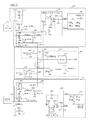
FIG. 2 , a known semiconductor integratedcircuit 1 is configured to generate rupture bias voltages therein. - The semiconductor integrated
circuit 1 includes powersupply control blocks fuse set 11. - The
fuse set 11 may be provided in a plural number, and eachfuse set 11 may include a plurality of electronic fuses. - The power supply control blocks 12 and 13 generate rupture bias voltages VPPF and VBBF using internal power sources VPP and VBB, respectively.
- Here, the internal power sources VPP and VBB are power sources which are internally generated by a VPP pump (not shown) and a VBB pump (not shown), respectively.
- In this regard, in the case where the rupture bias voltages VPPF and VBBF are generated using the internal power sources VPP and VBB, when compared to the case where the rupture bias voltages VPPF and VBBF are not generated internally using the internal power sources VPP and VBB, an increased number of charge pumps are needed. As a consequence, a circuit area increases, and it may be difficult to supply precise and stable rupture bias voltages.
- Referring to
FIG. 3 , a known semiconductor integratedcircuit 2 is configured to receive rupture bias voltages VPPF and VBBF from an external test equipment. - The semiconductor integrated
circuit 2 includesdedicated terminals supply control blocks 14 and 15, and afuse set 11. - The
dedicated terminals - The
dedicated terminals - Also, the power
supply control blocks 14 and 15 provide the rupture bias voltages VPPF and VBBF supplied through thededicated terminals - However, due to the area of the
dedicated terminals - A semiconductor integrated circuit which can supply stable rupture bias voltages and reduce the area of and improve the design efficiency of a circuit associated with power supply terminals is described herein.
- In an embodiment of the present invention, a semiconductor integrated circuit includes: a fuse set; a terminal assigned to be applied with a first external signal in a normal operation; and a control unit configured to receive a second external signal through the terminal and apply the received second external signal to the fuse set in a fuse control operation.
- In an embodiment of the present invention, a semiconductor integrated circuit includes: a fuse set; a first terminal assigned to be applied with a first external signal in a normal operation; a first control unit configured to receive a second external signal through the first terminal and apply the received second external signal to the fuse set in a fuse rupture operation; a second terminal assigned to be applied with a third external signal in the normal operation; and a second control unit configured to receive a fourth external signal through the second terminal and apply the received fourth external signal to the fuse set in the fuse rupture operation.
- Features, aspects, and embodiments are described in conjunction with the attached drawings, in which:
-
FIG. 1 is a cross-sectional view illustrating a known electronic fuse; -
FIG. 2 is a block diagram showing a known semiconductor integrated circuit; -
FIG. 3 is a block diagram showing another known semiconductor integrated circuit; -
FIG. 4 is a block diagram showing a semiconductor integrated circuit in accordance with an embodiment of the present invention; -
FIGS. 5 to 7 are circuit diagrams of exemplary embodiments of the semiconductor integrated circuit shown inFIG. 4 ; -
FIG. 8 is a block diagram showing a semiconductor integrated circuit in accordance with an embodiment of the present invention; -
FIG. 9 is a circuit diagram of the semiconductor integrated circuit shown inFIG. 8 ; -
FIG. 10 is a block diagram showing a semiconductor integrated circuit in accordance with an embodiment of the present invention; and -
FIG. 11 is a circuit diagram of the semiconductor integrated circuit shown inFIG. 10 . - Hereinafter, a semiconductor integrated circuit according to the present invention will be described below with reference to the accompanying drawings through exemplary embodiments.
- In an embodiments of the present invention, dedicated terminals for rupture bias voltages are not used, and instead, through terminals assigned for a normal operation, first external signals are received in a normal operation and second external signals are received in a fuse control operation, e.g., a fuse rupture operation, to be applied to a selected fuse.
- Embodiments of the present invention exemplify the case of using terminals which are assigned for a normal operation and are not used in a test operation, and in particular, exemplify the case of using terminals which receive reference voltages as the first external is signals.
- Also, Embodiments of the present invention exemplify the case in which rupture bias voltages are supplied as second external signals.
- Here, the reference voltages may be used for determining the respective values of data and an address inputted to a semiconductor integrated circuit.
-
FIG. 4 is a block diagram showing a semiconductor integrated circuit in accordance with an embodiment of the present invention. - Referring to
FIG. 4 , a semiconductor integratedcircuit 100 in accordance with an embodiment of the present invention includes first andsecond terminals control unit 200, and afuse set 500. - The
first terminal 130 receives a voltage from a controller which is electrically connected with the semiconductor integratedcircuit 100 in a normal operation. In the normal operation, the controller may provide a first reference voltage VREF_DQ with a preset level (for example, VDD/2) to thefirst terminal 130. - The
first terminal 130 may be provided with a voltage from a test equipment in a fuse rupture operation. In the fuse rupture operation, the test equipment may provide a first rupture bias voltage VRUPTP which has a different level from a voltage level of an operation voltage in the normal operation, e.g., the same level as the rupture bias voltage VPPF described above with reference toFIG. 3 , to thefirst terminal 130. - The
second terminal 140 receives a voltage from the controller which is electrically connected with the semiconductor integratedcircuit 100 in the normal operation. In the normal operation, the controller may provide a second reference voltage VREF_CA with a preset level (for example, VDD/2) to thesecond terminal 140. - The
second terminal 140 may be provided with a voltage from the test equipment in the fuse rupture operation. In the fuse rupture operation, the test equipment may provide a second rupture bias voltage VRUPTB which has a different level from a voltage level of an operation voltage in the normal operation, e.g., the same level as the rupture bias voltage VBBF described above with reference toFIG. 3 , to thesecond terminal 140. - The
control unit 200 is configured to couple the first andsecond terminals - According to an example, the
control unit 200 electrically connects the first andsecond terminals - Also, the
control unit 200 electrically connects the first andsecond terminals buffers - The
control unit 200 may include afirst control unit 300 and asecond control unit 400. - The
first control unit 300 is configured to provide the first rupture bias voltage VRUPTP inputted through thefirst terminal 130, to the fuse set 500 in response to the test mode signal TM. - According to an example, the
first control unit 300 is configured to provide a first reference voltage VREF_DQ inputted through thefirst terminal 130, to thebuffer 110 in response to the deactivation of the test mode signal TM. - Also, the
first control unit 300 may be configured to generate an internal voltage VDD1 and provide the generated internal voltage VDD1 to the fuse set 500. - According to an example, the
second control unit 400 is configured to provide the voltage inputted through thesecond terminal 140, to the fuse set 500 as the second rupture bias voltage VRUPTB in response to the activation of the test mode signal TM. - Also, the
second control unit 400 is configured to provide a second reference voltage VREF_CA inputted through thesecond terminal 140, to thebuffer 120 in response to the deactivation of the test mode signal TM. - Further, the
second control unit 400 may be configured to generate an internal voltage VSS1 and provide the generated internal voltage VSS1 to the fuse set 500. - The first rupture bias voltage VRUPTP may have a level higher than a pumping voltage VPP. The second rupture bias voltage VRUPTB may be a negative voltage which has a level lower than a bulk bias voltage VBB.
- The first and second rupture bias voltages VRUPTP and VRUPTB may have the same levels as the rupture bias voltages VPPF and VBBF described above with reference to
FIG. 3 . - The fuse set 500 may be provided in a plural number, and each fuse set 500 may include a plurality of electronic fuses.
- The fuse set 500 is configured to receive the test mode signal TM, fuse address signals ADD<0:N>, a power-up signal PWRUP, the first and second rupture bias voltages VRUPTP and VRUPTB, and the internal voltages VDD1 and VSS1.
- The fuse set 500 is configured to apply the first and second rupture bias voltages VRUPTP and VRUPTB to a selected fuse in response to the fuse address signals ADD<0:N>, and change the state of the fuse.
- The fuse set 500 is configured to block supply of the first and second rupture bias voltages VRUPTP and VRUPTB to unselected fuses according to the fuse address signals ADD<0:N>.
- The
buffers -
FIG. 5 is a circuit diagram of an exemplary embodiment 100-1 of the semiconductor integratedcircuit 100 shown inFIG. 4 . - Referring to
FIG. 5 , thefirst control unit 300 includes a floating preventingsection 310, alevel shifter 320, an internalvoltage generating section 330, and a plurality ofswitches - The floating preventing
section 310 may prevent a first reference voltage terminal VREF_DQIN from being floated by applying the voltage (for example, VDD/2), generated when first and second test mode signals TM and TMb are activated, to the first reference voltage terminal VREF_DQIN. - Here, the first test mode signal TM may be defined in such a manner that it is activated when it has a logic high level and is deactivated when it has a logic low level. The second test mode signal TMb may be generated by inverting the test mode signal TM and may be defined in such a manner that it is deactivated when it has a logic high level and is activated when it has a logic low level.
- The
level shifter 320 is configured to generate third and fourth test mode signals TMH and TMHb in response to the first and second test mode signals TM and TMb. - The
level shifter 320 generates the third and fourth test mode signals TMH and TMHb using a ground voltage VSS and a voltage applied to afirst terminal 130. - The third test mode signal TMH is a signal which has substantially the same phase as the first test mode signal TM and has a larger voltage level than the first test mode signal TM. The fourth test mode signal TMHb is a signal which may be generated by inverting the third test mode signal TMH.
- For example, if the first test mode signal TM has a level between the ground voltage VSS and an external voltage VDD, the third test mode signal TMH may have a level between the ground voltage VSS and the first rupture bias voltage VRUPTP.
- The internal
voltage generating section 330 is configured to output the external voltage VDD or the voltage of thefirst terminal 130 as the internal voltage VDD1 in response to the test mode signals TM, TMb, TMH and TMHb. - The internal
voltage generating section 330 outputs the voltage of thefirst terminal 130 as the internal voltage VDD1 when the third and first test mode signals TMH and TM are activated. At this time, when the test mode signals TMH and TM are activated, the first rupture bias voltage VRUPTP may be inputted through thefirst terminal 130. Therefore, when the test mode signals TMH and TM are activated, the voltage value of the internal voltage VDD1 is substantially the same as the first rupture bias voltage VRUPTP. - The internal
voltage generating section 330 outputs the external voltage VDD as the internal voltage VDD1 when the third and first test mode signals TMH and TM are deactivated. - The
switch 340 transmits a first reference voltage VREF_DQ, inputted through thefirst terminal 130, to thebuffer 110 when the test mode signal TMH is deactivated. - The
switch 350 transmits the first rupture bias voltage VRUPTP, inputted through thefirst terminal 130, to the fuse set 500 when the test mode signal TMH is activated. - The
second control unit 400 includes a floating preventingsection 410, alevel shifter 420, an internalvoltage generating section 430, and a plurality ofswitches - The floating preventing
section 410 may prevent a second reference voltage terminal VREF_CAIN from being floated by applying the voltage (for example, VDD/2), generated when the first and second test mode signals TM and TMb are activated, to the second reference voltage terminal VREF_CAIN. - The
level shifter 420 is configured to generate fifth and sixth test mode signals TML and TMLb in response to the first and second test mode signals TM and TMb. - The
level shifter 420 generates the fifth and sixth test mode signals TML and TMLb using the external voltage VDD and a voltage applied to asecond terminal 140. - The fifth test mode signal TML is a signal which has substantially the same phase as the first test mode signal TM and has a smaller voltage level than the first test mode signal TM. The sixth test mode signal TMLb is a signal which may be generated by inverting the fifth test mode signal TML.
- For example, if the first test mode signal TM has a level between the external voltage VDD and the ground voltage VSS, the fifth test mode signal TML may have a level between the external voltage VDD and the second rupture bias voltage VRUPTB.
- The first and second test mode signals TM and TMb, which are provided from an outside, may be referred to as external test mode signals. On the other hand, the test mode signals TMH, TMHb, TML and TMLb, which are generated internally, may be referred to as internal test mode signals.
- The internal
voltage generating section 430 is configured to output the ground voltage VSS or the voltage of thesecond terminal 140 as the internal voltage VSS1 in response to the test mode signals TM, TMb, TML and TMLb. - The internal
voltage generating section 430 outputs the voltage of thesecond terminal 140 as the internal voltage VSS1 when the fifth and first test mode signals TML and TM are activated. At this time, when the test mode signals TML and TM are activated, the second rupture bias voltage VRUPTB may be inputted through thesecond terminal 140. Therefore, when the test mode signals TML and TM are activated, the voltage value of the internal voltage VSS1 is substantially the same as the second rupture bias voltage VRUPTB. - The internal
voltage generating section 430 outputs the ground voltage VSS as the internal voltage VSS1 when the fifth and first test mode signals TML and TM are deactivated. - The
switch 440 transmits a second reference voltage VREF_CA, inputted through thesecond terminal 140, to thebuffer 120 when the test mode signal TM is deactivated. - The
switch 450 transmits the second rupture bias voltage VRUPTB, inputted through thesecond terminal 140, to the fuse set 500 when the test mode signal TM is activated. - The fuse set 500 includes a
fuse 510, a fusestate detecting section 520, and a plurality ofswitches -
FIG. 5 shows afuse 510 among a plurality of fuses included in the fuse set 500 andcircuit components - Here, an electronic fuse may be used as the
fuse 510. - The fuse
state detecting section 520 is configured to determine whether or not rupture of thefuse 510 has normally occurred and generate a fuse state signal F_ADD. - The fuse
state detecting section 520 includes asensor 521,transistors inverter 524. - The
transistor 522 precharges the gate (hereinafter, referred to as one end) of thefuse 510 to the level of the external voltage VDD in response to activation of the power-up signal PWRUP. - The
transistor 523 electrically connects the terminal of thefuse 510 to which a source, a drain and a bulk are connected (hereinafter, referred to as the other end) (seeFIG. 1 ) to a ground terminal after the fuse rupture operation, that is, after deactivation of the test mode signal TM. - If the rupture of the
fuse 510 has normally occurred, the one end and the other end of thefuse 510 are electrically connected with each other. Accordingly, the voltage level of thefuse 510 will be lowered. - However, if the rupture of the
fuse 510 has not normally occurred, the one end and the other end of thefuse 510 are not electrically connected with each other, otherwise, even though they are electrically connected with each other, the voltage level of thefuse 510 may not be appropriately lowered when compared to a normal case. - Accordingly, the
sensor 521 may determine whether or not is the rupture of thefuse 510 has normally occurred, depending upon a change in the voltage level of the gate of thefuse 510, and generate the fuse state signal F_ADD as a determination result. - The plurality of
switches fuse 510 in response to the test mode signal TM and a fuse address signal ADD<i> (i is one of 0 to N). - The fuse address signal ADD<i> is an address signal for selecting the
fuse 510. - The
switch 550 applies the first rupture bias voltage VRUPTP to the one end of thefuse 510 only when both the test mode signal TM and the fuse address signal ADD<i> are activated. - The
switch 550 includes aNAND gate 551 and atransistor 552. - The
switch 560 applies the second rupture bias voltage VRUPTB to the other end of thefuse 510 only when both the test mode signal TM and the fuse address signal ADD<i> are activated. - The
switch 560 includes aNAND gate 561, aninverter 562 and atransistor 563. - In an embodiment of the present invention, as a difference between the first and second rupture bias voltages VRUPTP and VRUPTB applied to both ends of the
fuse 510 increases, the rupture of thefuse 510 may stably occur. - A voltage higher than the pumping voltage VPP may be applied as the first rupture bias voltage VRUPTP, and a negative voltage lower than the bulk bias voltage VBB may be applied as the second rupture bias voltage VRUPTB.
- In an embodiment of the present invention, the first and second rupture bias voltages VRUPTP and VRUPTB are not applied to the
buffers - Accordingly, in order to secure the off characteristics of the pass gates constituting the
switches switches - Further, in order to secure the off characteristics of the pass gates constituting the
switches switches - Similarly, in order to secure the off characteristics of the
transistor 552 of theswitch 550, the internal voltage VDD1 with the level of the first rupture bias voltage VRUPTP instead of the external voltage VDD may be applied to the power source terminal of theNAND gate 551. - Further, in order to secure the off characteristics of the
transistor 563 of theswitch 560, the internal voltage VDD1 with the level of the second rupture bias voltage VRUPTB instead of the ground voltage VSS may be applied to the ground terminals of theNAND gate 561 and theinverter 562. -
FIG. 6 is a circuit diagram of an exemplary embodiment 100-2 of the semiconductor integratedcircuit 100 shown inFIG. 4 . - Referring to
FIG. 6 , the semiconductor integrated circuit 100-2 includes afirst control unit 301, asecond control unit 401, and afuse set 500. - The
first control unit 301 includes a floating preventingsection 310, alevel shifter 320, an internalvoltage generating section 330, and a plurality ofswitches - The plurality of
switches - The floating preventing
section 310, thelevel shifter 320 and the internalvoltage generating section 330 may be configured in the same manner as inFIG. 5 . - The
second control unit 401 includes a floating preventingsection 410, alevel shifter 420, an internalvoltage generating section 430, and a plurality ofswitches - The plurality of
switches - The floating preventing
section 410, thelevel shifter 420 and the internalvoltage generating section 430 may be configured in the same manner as inFIG. 5 . - The fuse set 500 may be configured in the same manner as to in
FIG. 5 . -
FIG. 7 is a circuit diagram of an exemplary embodiment 100-3 of the semiconductor integratedcircuit 100 shown inFIG. 4 . - Referring to
FIG. 7 , the semiconductor integrated circuit 100-3 includes afirst control unit 302, asecond control unit 402, and is afuse set 500. - The
first control unit 302 includes a floating preventingsection 311, alevel shifter 320, an internalvoltage generating section 330, a plurality ofswitches feedback circuit section 360. - The
feedback circuit section 360 is configured to maintain, through feedback, node voltages Node_A and Node_B generated in response to the power-up signal PWRUP. At this time, the first test mode signal TM is in a deactivated state. - The
feedback circuit section 360 is configured to change the levels of the node voltages Node_A and Node_B using a first rupture bias voltage VRUPTP which is inputted in response to activation of the first test mode signal TM. - The
switch 342 is controlled by the node voltages Node_A and Node_B. - The
switch 352 is controlled by the first and second test mode signals TM and TMb. - The
level shifter 320 and the internalvoltage generating section 330 may be configured in the same manner as inFIG. 5 . - The
second control unit 402 includes a floating preventingsection 411, alevel shifter 420, an internalvoltage generating section 430, a plurality ofswitches 442 and 452, and afeedback circuit section 460. - The
feedback circuit section 460 is configured to maintain, through feedback, node voltages Node_C and Node_D generated in response to a power-up signal PWRUPb. At this time, the first test mode signal TM is in a deactivated state. - The
feedback circuit section 460 is configured to change the levels of the node voltages Node_C and Node_D using the second rupture bias voltage VRUPTB which is inputted in response to activation of the first test mode signal TM. - The switch 442 is controlled by the node voltages Node_C and Node_D.
- The
switch 452 is controlled by the first and second test mode signals TM and TMb. - The
level shifter 420 and the internalvoltage generating section 430 may be configured in the same manner as inFIG. 5 . - The fuse set 500 may be configured in the same manner as in
FIG. 5 . - In a semiconductor integrated
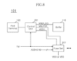
circuit 101 in accordance with an embodiment of the present invention shown inFIG. 8 , afirst terminal 130, which is used to supply a reference voltage in a normal operation, may be used to receive a first rupture bias voltage VRUPTP which is applied to one end of a fuse in a fuse rupture operation. As the voltage applied to the other end of the fuse, a ground voltage VSS, (or VBB) which is to be used in a normal operation, may be used. - Referring to
FIG. 8 , the semiconductor integratedcircuit 101 in accordance with an embodiment of the present invention includes afirst terminal 130, acontrol unit 201, and afuse set 501. - The semiconductor integrated
circuit 101 may further include abuffer 110. - The
buffer 110 may buffer a first reference voltage VREF_DQ and provide the first reference voltage VREF_DQ to a circuit component (not shown) which is to receive data. - Referring to
FIG. 9 , thecontrol unit 201 includes a floating preventingsection 310, alevel shifter 320, an internalvoltage generating section 330, and a plurality ofswitches first control unit 300 shown inFIG. 5 . - The fuse set 501 includes a
fuse 510, a fusestate detecting section 520, and a plurality ofswitches - The
switch 570 includes aNAND gate 571, aninverter 572, and atransistor 573. - In the
switch 570, since theNAND gate 571 and theinverter 572 function to control thetransistor 573 for applying the ground voltage VSS (or VBB) to thefuse 510, they receive an external voltage VDD and the ground voltage VSS (or VBB) as power supply voltages. - The
fuse 510, the fusestate detecting section 520 and theswitch 550 may be configured in the same manner as inFIG. 5 . - In a semiconductor integrated
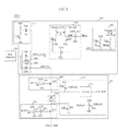
circuit 102 in accordance with an embodiment of the present invention shown inFIG. 10 , asecond terminal 140, which is used to supply a reference voltage in a normal operation, may be used to receive a second rupture bias voltage VRUPTB which is applied to the other end of the a fuse in a fuse rupture operation. Also, as the voltage applied to one end of the fuse, an external voltage VDD (or VPP) which is to be used in a normal operation, may be used. - Referring to
FIG. 10 , the semiconductor integratedcircuit 102 in accordance with an embodiment of the present invention includes asecond terminal 140, acontrol unit 202, and afuse set 502. - The semiconductor integrated
circuit 102 may further include abuffer 120. - The
buffer 120 may buffer a second reference voltage VREF_CA and provide the second reference voltage VREF_CA to a circuit component (not shown) which is to receive data. - Referring to
FIG. 11 , thecontrol unit 202 includes a floating preventingsection 410, alevel shifter 420, an internalvoltage generating section 430, and a plurality ofswitches second control unit 400 shown inFIG. 5 . - The fuse set 502 includes a
fuse 510, a fusestate detecting section 520, and a plurality ofswitches - The
switch 580 includes aNAND gate 581 and atransistor 582. - In the
switch 580, since theNAND gate 581 functions to control thetransistor 582 for applying the external voltage VDD (or VPP) to thefuse 510, theNAND gate 581 receives the external voltage VDD (or VPP) and a ground voltage VSS as power supply voltages. - The
fuse 510, the fusestate detecting section 520 and theswitch 550 may be configured in the same manner as inFIG. 5 . - In the embodiments of the present invention shown in
FIGS. 5 to 11 , it was described that theswitches state detecting section 520 are included in the fuse sets 500, 501 and 502. - However, such examples are only for an illustration purpose. Therefore, when considering functional aspects and changes in a circuit design, it is conceivable that the
switches state detecting section 520 may be included in thecontrol units - As is apparent from the above descriptions, in the embodiments of the present invention, without additionally forming or assigning terminals, it is possible to provide stable rupture bias voltages to a fuse.
- While certain embodiments have been described above, it will be understood to those skilled in the art that the embodiments described are by way of example only. Accordingly, the semiconductor integrated circuit described herein should not be limited based on the described embodiments. Rather, the semiconductor integrated circuit described herein should only be limited in light of the claims that follow when taken in conjunction with the above description and accompanying drawings.
Claims (30)
Applications Claiming Priority (2)
| Application Number | Priority Date | Filing Date | Title |
|---|---|---|---|
| KR1020110027575A KR101240256B1 (en) | 2011-03-28 | 2011-03-28 | Semiconductor integrated circuit |
| KR10-2011-0027575 | 2011-03-28 |
Publications (2)
| Publication Number | Publication Date |
|---|---|
| US20120249221A1 true US20120249221A1 (en) | 2012-10-04 |
| US8598943B2 US8598943B2 (en) | 2013-12-03 |
Family
ID=46901613
Family Applications (1)
| Application Number | Title | Priority Date | Filing Date |
|---|---|---|---|
| US13/219,636 Active 2031-09-29 US8598943B2 (en) | 2011-03-28 | 2011-08-27 | Semiconductor integrated circuit with stable rupture voltage fuse |
Country Status (4)
| Country | Link |
|---|---|
| US (1) | US8598943B2 (en) |
| KR (1) | KR101240256B1 (en) |
| CN (1) | CN102708924B (en) |
| TW (1) | TWI541969B (en) |
Cited By (1)
| Publication number | Priority date | Publication date | Assignee | Title |
|---|---|---|---|---|
| US20250234529A1 (en) * | 2024-01-16 | 2025-07-17 | Synopsys, Inc. | One-time programmable bitcell with a thermally enhanced rupture |
Families Citing this family (3)
| Publication number | Priority date | Publication date | Assignee | Title |
|---|---|---|---|---|
| KR102016727B1 (en) * | 2013-04-24 | 2019-09-02 | 에스케이하이닉스 주식회사 | Semiconductor memory apparatus and method of controlling external voltage using the same |
| CN106328187A (en) * | 2016-08-31 | 2017-01-11 | 西安紫光国芯半导体有限公司 | Dynamic random access memory chip e-fuse operating-voltage generating circuit and method |
| US10763662B2 (en) * | 2017-10-10 | 2020-09-01 | Littelfuse, Inc. | Self-powered electronic fuse |
Citations (18)
| Publication number | Priority date | Publication date | Assignee | Title |
|---|---|---|---|---|
| US5144578A (en) * | 1988-05-27 | 1992-09-01 | Matsushita Electric Industrial Co., Ltd. | Semiconductor device having multiple supply potential paths for reducing electrical interference between circuits contained therein |
| US5712577A (en) * | 1996-04-18 | 1998-01-27 | Electronics And Telecommunications Research Institute | Anti-fuse programming circuit for user programmable integrated |
| US6144247A (en) * | 1998-06-30 | 2000-11-07 | Hyundai Electronics Industries Co., Ltd. | Anti-fuse programming circuit using variable voltage generator |
| US6150864A (en) * | 1998-08-24 | 2000-11-21 | Yach; Randy L. | Time delay circuit which is voltage independent |
| US6657531B2 (en) * | 2000-12-27 | 2003-12-02 | Kabushiki Kaisha Toshiba | Fuse circuit using capacitors as fuse elements |
| US6680873B2 (en) * | 2001-01-12 | 2004-01-20 | Kabushiki Kaisha Toshiba | Semiconductor device having electric fuse element |
| US7035158B2 (en) * | 2002-11-26 | 2006-04-25 | Kabushiki Kaisha Toshiba | Semiconductor memory with self fuse programming |
| US7050349B2 (en) * | 2001-06-25 | 2006-05-23 | Renesas Technology Corp. | Semiconductor integrated circuit device and semiconductor memory device reprogrammable after assembly |
| US7349281B2 (en) * | 2005-09-09 | 2008-03-25 | Kabushiki Kaisha Toshiba | Anti-fuse memory circuit |
| US7376036B2 (en) * | 2005-02-09 | 2008-05-20 | Nec Electronics Corporation | Semiconductor device including fuse and method for testing the same capable of suppressing erroneous determination |
| US7394715B1 (en) * | 2006-01-11 | 2008-07-01 | Mediatek Inc. | Memory system comprising memories with different capacities and storing and reading method thereof |
| US7394713B2 (en) * | 2005-04-27 | 2008-07-01 | Infineon Technologies Ag | Fuse memory cell with improved protection against unauthorized access |
| US7551497B2 (en) * | 2007-09-20 | 2009-06-23 | Mediatek Inc. | Memory circuits preventing false programming |
| US20090284310A1 (en) * | 2004-02-06 | 2009-11-19 | Semiconductor Energy Laboratory Co., Ltd. | Semiconductor device |
| US20100109683A1 (en) * | 2008-10-31 | 2010-05-06 | Elpida Memory, Inc. | Semiconductor device |
| US7932738B1 (en) * | 2010-05-07 | 2011-04-26 | Power Integrations, Inc. | Method and apparatus for reading a programmable anti-fuse element in a high-voltage integrated circuit |
| US8299845B2 (en) * | 2009-09-16 | 2012-10-30 | Elpida Memory, Inc. | Semiconductor device |
| US8305826B2 (en) * | 2010-05-07 | 2012-11-06 | Power Integrations, Inc. | Method and apparatus for programming an anti-fuse element in a high-voltage integrated circuit |
Family Cites Families (4)
| Publication number | Priority date | Publication date | Assignee | Title |
|---|---|---|---|---|
| KR19990076398A (en) * | 1998-03-31 | 1999-10-15 | 윤종용 | Internal Information Display Circuit of Semiconductor Device |
| KR100322526B1 (en) * | 1999-01-14 | 2002-03-18 | 윤종용 | Input circuit having a fuse therein and a semiconductor device having the same |
| KR100594204B1 (en) * | 1999-09-21 | 2006-06-28 | 삼성전자주식회사 | Input circuit of semiconductor device with cavity pad |
| KR101608739B1 (en) * | 2009-07-14 | 2016-04-21 | 삼성전자주식회사 | Redundancy circuit, semiconductor memory device including the same and a repairing method of a semiconductor memory device |
-
2011
- 2011-03-28 KR KR1020110027575A patent/KR101240256B1/en not_active Expired - Fee Related
- 2011-08-27 US US13/219,636 patent/US8598943B2/en active Active
- 2011-09-23 TW TW100134427A patent/TWI541969B/en not_active IP Right Cessation
- 2011-10-26 CN CN201110329165.XA patent/CN102708924B/en active Active
Patent Citations (18)
| Publication number | Priority date | Publication date | Assignee | Title |
|---|---|---|---|---|
| US5144578A (en) * | 1988-05-27 | 1992-09-01 | Matsushita Electric Industrial Co., Ltd. | Semiconductor device having multiple supply potential paths for reducing electrical interference between circuits contained therein |
| US5712577A (en) * | 1996-04-18 | 1998-01-27 | Electronics And Telecommunications Research Institute | Anti-fuse programming circuit for user programmable integrated |
| US6144247A (en) * | 1998-06-30 | 2000-11-07 | Hyundai Electronics Industries Co., Ltd. | Anti-fuse programming circuit using variable voltage generator |
| US6150864A (en) * | 1998-08-24 | 2000-11-21 | Yach; Randy L. | Time delay circuit which is voltage independent |
| US6657531B2 (en) * | 2000-12-27 | 2003-12-02 | Kabushiki Kaisha Toshiba | Fuse circuit using capacitors as fuse elements |
| US6680873B2 (en) * | 2001-01-12 | 2004-01-20 | Kabushiki Kaisha Toshiba | Semiconductor device having electric fuse element |
| US7050349B2 (en) * | 2001-06-25 | 2006-05-23 | Renesas Technology Corp. | Semiconductor integrated circuit device and semiconductor memory device reprogrammable after assembly |
| US7035158B2 (en) * | 2002-11-26 | 2006-04-25 | Kabushiki Kaisha Toshiba | Semiconductor memory with self fuse programming |
| US20090284310A1 (en) * | 2004-02-06 | 2009-11-19 | Semiconductor Energy Laboratory Co., Ltd. | Semiconductor device |
| US7376036B2 (en) * | 2005-02-09 | 2008-05-20 | Nec Electronics Corporation | Semiconductor device including fuse and method for testing the same capable of suppressing erroneous determination |
| US7394713B2 (en) * | 2005-04-27 | 2008-07-01 | Infineon Technologies Ag | Fuse memory cell with improved protection against unauthorized access |
| US7349281B2 (en) * | 2005-09-09 | 2008-03-25 | Kabushiki Kaisha Toshiba | Anti-fuse memory circuit |
| US7394715B1 (en) * | 2006-01-11 | 2008-07-01 | Mediatek Inc. | Memory system comprising memories with different capacities and storing and reading method thereof |
| US7551497B2 (en) * | 2007-09-20 | 2009-06-23 | Mediatek Inc. | Memory circuits preventing false programming |
| US20100109683A1 (en) * | 2008-10-31 | 2010-05-06 | Elpida Memory, Inc. | Semiconductor device |
| US8299845B2 (en) * | 2009-09-16 | 2012-10-30 | Elpida Memory, Inc. | Semiconductor device |
| US7932738B1 (en) * | 2010-05-07 | 2011-04-26 | Power Integrations, Inc. | Method and apparatus for reading a programmable anti-fuse element in a high-voltage integrated circuit |
| US8305826B2 (en) * | 2010-05-07 | 2012-11-06 | Power Integrations, Inc. | Method and apparatus for programming an anti-fuse element in a high-voltage integrated circuit |
Cited By (2)
| Publication number | Priority date | Publication date | Assignee | Title |
|---|---|---|---|---|
| US20250234529A1 (en) * | 2024-01-16 | 2025-07-17 | Synopsys, Inc. | One-time programmable bitcell with a thermally enhanced rupture |
| US12446215B2 (en) * | 2024-01-16 | 2025-10-14 | Synopsys, Inc. | One-time programmable bitcell with a thermally enhanced rupture |
Also Published As
| Publication number | Publication date |
|---|---|
| KR101240256B1 (en) | 2013-03-11 |
| KR20120109205A (en) | 2012-10-08 |
| TWI541969B (en) | 2016-07-11 |
| CN102708924A (en) | 2012-10-03 |
| CN102708924B (en) | 2016-12-21 |
| US8598943B2 (en) | 2013-12-03 |
| TW201240049A (en) | 2012-10-01 |
Similar Documents
| Publication | Publication Date | Title |
|---|---|---|
| US8390342B2 (en) | High voltage switch circuit of semiconductor device | |
| US8598943B2 (en) | Semiconductor integrated circuit with stable rupture voltage fuse | |
| US8258856B2 (en) | Antifuse circuit having protection circuit | |
| US9142319B2 (en) | Semiconductor device employing fuse programming | |
| US8692604B2 (en) | Impedance calibration circuit | |
| US7376036B2 (en) | Semiconductor device including fuse and method for testing the same capable of suppressing erroneous determination | |
| US7417475B2 (en) | Circuit and method for generating power up signal | |
| US20130147545A1 (en) | Reference voltage generation circuit and internal voltage generation circuit using the same | |
| US9323260B2 (en) | Internal voltage generation circuits and semiconductor devices including the same | |
| US9557788B2 (en) | Semiconductor memory device including array e-fuse | |
| US8289070B2 (en) | Fuse circuit | |
| US8570094B2 (en) | Semiconductor integrated circuit and method for driving the same | |
| US7902902B2 (en) | Anti-fuse repair control circuit for preventing stress on circuit parts | |
| US9793009B2 (en) | Repair information storage circuit and semiconductor apparatus including the same | |
| US8854779B2 (en) | Integrated circuit | |
| US8649237B2 (en) | Power-up signal generation circuit | |
| KR100757411B1 (en) | Voltage reset circuit and method of semiconductor memory device using optional fuse circuit | |
| KR20140085245A (en) | Semiconductor device with fuse sensing circuit | |
| US8724409B2 (en) | Semiconductor integrated circuit | |
| US8717087B2 (en) | Anti-fuse circuit | |
| KR102631894B1 (en) | Anti-fuse array for reducinf leakage current in anti-fuse cell | |
| KR20160049829A (en) | Apparatus for adjusting delay and operating apparatus including the same | |
| US9893612B2 (en) | Voltage generation circuit | |
| KR20120082635A (en) | Semiconductor apparatus |
Legal Events
| Date | Code | Title | Description |
|---|---|---|---|
| AS | Assignment |
Owner name: HYNIX SEMICONDUCTOR INC., KOREA, REPUBLIC OF Free format text: ASSIGNMENT OF ASSIGNORS INTEREST;ASSIGNORS:OH, SANG MOOK;IM, JAE HYUK;REEL/FRAME:026818/0096 Effective date: 20110722 |
|
| FEPP | Fee payment procedure |
Free format text: PAYOR NUMBER ASSIGNED (ORIGINAL EVENT CODE: ASPN); ENTITY STATUS OF PATENT OWNER: LARGE ENTITY |
|
| STCF | Information on status: patent grant |
Free format text: PATENTED CASE |
|
| FPAY | Fee payment |
Year of fee payment: 4 |
|
| MAFP | Maintenance fee payment |
Free format text: PAYMENT OF MAINTENANCE FEE, 8TH YEAR, LARGE ENTITY (ORIGINAL EVENT CODE: M1552); ENTITY STATUS OF PATENT OWNER: LARGE ENTITY Year of fee payment: 8 |
|
| MAFP | Maintenance fee payment |
Free format text: PAYMENT OF MAINTENANCE FEE, 12TH YEAR, LARGE ENTITY (ORIGINAL EVENT CODE: M1553); ENTITY STATUS OF PATENT OWNER: LARGE ENTITY Year of fee payment: 12 |