US10763383B2 - Nano-metal connections for a solar cell array - Google Patents
Nano-metal connections for a solar cell array Download PDFInfo
- Publication number
- US10763383B2 US10763383B2 US15/643,287 US201715643287A US10763383B2 US 10763383 B2 US10763383 B2 US 10763383B2 US 201715643287 A US201715643287 A US 201715643287A US 10763383 B2 US10763383 B2 US 10763383B2
- Authority
- US
- United States
- Prior art keywords
- nano
- solar cell
- substrate
- metal
- metal material
- Prior art date
- Legal status (The legal status is an assumption and is not a legal conclusion. Google has not performed a legal analysis and makes no representation as to the accuracy of the status listed.)
- Active, expires
Links
- 229910052751 metal Inorganic materials 0.000 title claims abstract description 73
- 239000002184 metal Substances 0.000 title claims abstract description 73
- 239000000758 substrate Substances 0.000 claims abstract description 99
- 239000007769 metal material Substances 0.000 claims abstract description 43
- 239000010949 copper Substances 0.000 claims abstract description 26
- 239000010931 gold Substances 0.000 claims abstract description 22
- 230000008018 melting Effects 0.000 claims abstract description 19
- 238000002844 melting Methods 0.000 claims abstract description 19
- 239000002105 nanoparticle Substances 0.000 claims abstract description 19
- 229910052737 gold Inorganic materials 0.000 claims abstract description 16
- 229910052709 silver Inorganic materials 0.000 claims abstract description 16
- 239000007787 solid Substances 0.000 claims abstract description 16
- 229910052802 copper Inorganic materials 0.000 claims abstract description 11
- RYGMFSIKBFXOCR-UHFFFAOYSA-N Copper Chemical compound [Cu] RYGMFSIKBFXOCR-UHFFFAOYSA-N 0.000 claims abstract description 5
- 229910052782 aluminium Inorganic materials 0.000 claims abstract description 5
- BQCADISMDOOEFD-UHFFFAOYSA-N Silver Chemical compound [Ag] BQCADISMDOOEFD-UHFFFAOYSA-N 0.000 claims abstract description 4
- XAGFODPZIPBFFR-UHFFFAOYSA-N aluminium Chemical compound [Al] XAGFODPZIPBFFR-UHFFFAOYSA-N 0.000 claims abstract description 4
- PCHJSUWPFVWCPO-UHFFFAOYSA-N gold Chemical compound [Au] PCHJSUWPFVWCPO-UHFFFAOYSA-N 0.000 claims abstract description 4
- 239000004332 silver Substances 0.000 claims abstract description 4
- 238000000034 method Methods 0.000 claims description 25
- 239000011888 foil Substances 0.000 claims description 15
- 239000002344 surface layer Substances 0.000 claims description 11
- 239000000956 alloy Substances 0.000 claims description 6
- 229910045601 alloy Inorganic materials 0.000 claims description 5
- 239000010944 silver (metal) Substances 0.000 claims description 5
- 238000007711 solidification Methods 0.000 claims description 5
- 230000008023 solidification Effects 0.000 claims description 5
- 238000010438 heat treatment Methods 0.000 abstract description 11
- 239000004020 conductor Substances 0.000 description 34
- 229910000679 solder Inorganic materials 0.000 description 32
- 239000010410 layer Substances 0.000 description 26
- 238000003466 welding Methods 0.000 description 12
- 238000004519 manufacturing process Methods 0.000 description 11
- 230000008569 process Effects 0.000 description 9
- 239000004642 Polyimide Substances 0.000 description 8
- 239000000463 material Substances 0.000 description 8
- 239000000203 mixture Substances 0.000 description 8
- 229920001721 polyimide Polymers 0.000 description 8
- 238000013459 approach Methods 0.000 description 7
- 238000003491 array Methods 0.000 description 7
- 230000008901 benefit Effects 0.000 description 7
- 239000000853 adhesive Substances 0.000 description 6
- 230000001070 adhesive effect Effects 0.000 description 6
- 238000013461 design Methods 0.000 description 6
- 239000002245 particle Substances 0.000 description 6
- 239000006059 cover glass Substances 0.000 description 5
- 150000002739 metals Chemical class 0.000 description 5
- 238000005476 soldering Methods 0.000 description 5
- 238000005382 thermal cycling Methods 0.000 description 5
- 230000005496 eutectics Effects 0.000 description 3
- 230000015572 biosynthetic process Effects 0.000 description 2
- 238000000151 deposition Methods 0.000 description 2
- 238000010586 diagram Methods 0.000 description 2
- 239000011159 matrix material Substances 0.000 description 2
- 230000004048 modification Effects 0.000 description 2
- 238000012986 modification Methods 0.000 description 2
- 229920000642 polymer Polymers 0.000 description 2
- 230000008439 repair process Effects 0.000 description 2
- 239000007858 starting material Substances 0.000 description 2
- 229910000846 In alloy Inorganic materials 0.000 description 1
- ATJFFYVFTNAWJD-UHFFFAOYSA-N Tin Chemical compound [Sn] ATJFFYVFTNAWJD-UHFFFAOYSA-N 0.000 description 1
- 229910000905 alloy phase Inorganic materials 0.000 description 1
- QVGXLLKOCUKJST-UHFFFAOYSA-N atomic oxygen Chemical compound [O] QVGXLLKOCUKJST-UHFFFAOYSA-N 0.000 description 1
- 238000006243 chemical reaction Methods 0.000 description 1
- 238000000576 coating method Methods 0.000 description 1
- 238000004891 communication Methods 0.000 description 1
- 238000001816 cooling Methods 0.000 description 1
- 238000000280 densification Methods 0.000 description 1
- 229910052732 germanium Inorganic materials 0.000 description 1
- GNPVGFCGXDBREM-UHFFFAOYSA-N germanium atom Chemical compound [Ge] GNPVGFCGXDBREM-UHFFFAOYSA-N 0.000 description 1
- 238000007689 inspection Methods 0.000 description 1
- 230000010354 integration Effects 0.000 description 1
- 238000012538 light obscuration Methods 0.000 description 1
- 238000012423 maintenance Methods 0.000 description 1
- 230000013011 mating Effects 0.000 description 1
- 239000000155 melt Substances 0.000 description 1
- 238000005457 optimization Methods 0.000 description 1
- 230000008520 organization Effects 0.000 description 1
- 238000012856 packing Methods 0.000 description 1
- 239000003973 paint Substances 0.000 description 1
- 230000003071 parasitic effect Effects 0.000 description 1
- 230000037361 pathway Effects 0.000 description 1
- 238000010587 phase diagram Methods 0.000 description 1
- 229920003223 poly(pyromellitimide-1,4-diphenyl ether) Polymers 0.000 description 1
- 238000010248 power generation Methods 0.000 description 1
- 238000012545 processing Methods 0.000 description 1
- 230000001737 promoting effect Effects 0.000 description 1
- 230000005855 radiation Effects 0.000 description 1
- 238000009419 refurbishment Methods 0.000 description 1
- 230000004044 response Effects 0.000 description 1
- 239000004065 semiconductor Substances 0.000 description 1
- 230000004083 survival effect Effects 0.000 description 1
- 238000012360 testing method Methods 0.000 description 1
- 230000009466 transformation Effects 0.000 description 1
- 239000011800 void material Substances 0.000 description 1
Images


Classifications
-
- H—ELECTRICITY
- H01—ELECTRIC ELEMENTS
- H01L—SEMICONDUCTOR DEVICES NOT COVERED BY CLASS H10
- H01L31/00—Semiconductor devices sensitive to infrared radiation, light, electromagnetic radiation of shorter wavelength or corpuscular radiation and specially adapted either for the conversion of the energy of such radiation into electrical energy or for the control of electrical energy by such radiation; Processes or apparatus specially adapted for the manufacture or treatment thereof or of parts thereof; Details thereof
- H01L31/02—Details
-
- H—ELECTRICITY
- H01—ELECTRIC ELEMENTS
- H01L—SEMICONDUCTOR DEVICES NOT COVERED BY CLASS H10
- H01L21/00—Processes or apparatus adapted for the manufacture or treatment of semiconductor or solid state devices or of parts thereof
- H01L21/02—Manufacture or treatment of semiconductor devices or of parts thereof
- H01L21/02104—Forming layers
- H01L21/02365—Forming inorganic semiconducting materials on a substrate
- H01L21/02436—Intermediate layers between substrates and deposited layers
- H01L21/02439—Materials
-
- H—ELECTRICITY
- H01—ELECTRIC ELEMENTS
- H01L—SEMICONDUCTOR DEVICES NOT COVERED BY CLASS H10
- H01L27/00—Devices consisting of a plurality of semiconductor or other solid-state components formed in or on a common substrate
- H01L27/14—Devices consisting of a plurality of semiconductor or other solid-state components formed in or on a common substrate including semiconductor components sensitive to infrared radiation, light, electromagnetic radiation of shorter wavelength or corpuscular radiation and specially adapted either for the conversion of the energy of such radiation into electrical energy or for the control of electrical energy by such radiation
- H01L27/142—Energy conversion devices
-
- H—ELECTRICITY
- H01—ELECTRIC ELEMENTS
- H01L—SEMICONDUCTOR DEVICES NOT COVERED BY CLASS H10
- H01L31/00—Semiconductor devices sensitive to infrared radiation, light, electromagnetic radiation of shorter wavelength or corpuscular radiation and specially adapted either for the conversion of the energy of such radiation into electrical energy or for the control of electrical energy by such radiation; Processes or apparatus specially adapted for the manufacture or treatment thereof or of parts thereof; Details thereof
- H01L31/02—Details
- H01L31/02002—Arrangements for conducting electric current to or from the device in operations
- H01L31/02005—Arrangements for conducting electric current to or from the device in operations for device characterised by at least one potential jump barrier or surface barrier
- H01L31/02008—Arrangements for conducting electric current to or from the device in operations for device characterised by at least one potential jump barrier or surface barrier for solar cells or solar cell modules
-
- H—ELECTRICITY
- H01—ELECTRIC ELEMENTS
- H01L—SEMICONDUCTOR DEVICES NOT COVERED BY CLASS H10
- H01L31/00—Semiconductor devices sensitive to infrared radiation, light, electromagnetic radiation of shorter wavelength or corpuscular radiation and specially adapted either for the conversion of the energy of such radiation into electrical energy or for the control of electrical energy by such radiation; Processes or apparatus specially adapted for the manufacture or treatment thereof or of parts thereof; Details thereof
- H01L31/02—Details
- H01L31/02016—Circuit arrangements of general character for the devices
- H01L31/02019—Circuit arrangements of general character for the devices for devices characterised by at least one potential jump barrier or surface barrier
- H01L31/02021—Circuit arrangements of general character for the devices for devices characterised by at least one potential jump barrier or surface barrier for solar cells
-
- H—ELECTRICITY
- H01—ELECTRIC ELEMENTS
- H01L—SEMICONDUCTOR DEVICES NOT COVERED BY CLASS H10
- H01L31/00—Semiconductor devices sensitive to infrared radiation, light, electromagnetic radiation of shorter wavelength or corpuscular radiation and specially adapted either for the conversion of the energy of such radiation into electrical energy or for the control of electrical energy by such radiation; Processes or apparatus specially adapted for the manufacture or treatment thereof or of parts thereof; Details thereof
- H01L31/02—Details
- H01L31/0224—Electrodes
- H01L31/022408—Electrodes for devices characterised by at least one potential jump barrier or surface barrier
- H01L31/022425—Electrodes for devices characterised by at least one potential jump barrier or surface barrier for solar cells
-
- H—ELECTRICITY
- H01—ELECTRIC ELEMENTS
- H01L—SEMICONDUCTOR DEVICES NOT COVERED BY CLASS H10
- H01L31/00—Semiconductor devices sensitive to infrared radiation, light, electromagnetic radiation of shorter wavelength or corpuscular radiation and specially adapted either for the conversion of the energy of such radiation into electrical energy or for the control of electrical energy by such radiation; Processes or apparatus specially adapted for the manufacture or treatment thereof or of parts thereof; Details thereof
- H01L31/0248—Semiconductor devices sensitive to infrared radiation, light, electromagnetic radiation of shorter wavelength or corpuscular radiation and specially adapted either for the conversion of the energy of such radiation into electrical energy or for the control of electrical energy by such radiation; Processes or apparatus specially adapted for the manufacture or treatment thereof or of parts thereof; Details thereof characterised by their semiconductor bodies
- H01L31/0352—Semiconductor devices sensitive to infrared radiation, light, electromagnetic radiation of shorter wavelength or corpuscular radiation and specially adapted either for the conversion of the energy of such radiation into electrical energy or for the control of electrical energy by such radiation; Processes or apparatus specially adapted for the manufacture or treatment thereof or of parts thereof; Details thereof characterised by their semiconductor bodies characterised by their shape or by the shapes, relative sizes or disposition of the semiconductor regions
- H01L31/035209—Semiconductor devices sensitive to infrared radiation, light, electromagnetic radiation of shorter wavelength or corpuscular radiation and specially adapted either for the conversion of the energy of such radiation into electrical energy or for the control of electrical energy by such radiation; Processes or apparatus specially adapted for the manufacture or treatment thereof or of parts thereof; Details thereof characterised by their semiconductor bodies characterised by their shape or by the shapes, relative sizes or disposition of the semiconductor regions comprising a quantum structures
- H01L31/035227—Semiconductor devices sensitive to infrared radiation, light, electromagnetic radiation of shorter wavelength or corpuscular radiation and specially adapted either for the conversion of the energy of such radiation into electrical energy or for the control of electrical energy by such radiation; Processes or apparatus specially adapted for the manufacture or treatment thereof or of parts thereof; Details thereof characterised by their semiconductor bodies characterised by their shape or by the shapes, relative sizes or disposition of the semiconductor regions comprising a quantum structures the quantum structure being quantum wires, or nanorods
-
- H—ELECTRICITY
- H01—ELECTRIC ELEMENTS
- H01L—SEMICONDUCTOR DEVICES NOT COVERED BY CLASS H10
- H01L31/00—Semiconductor devices sensitive to infrared radiation, light, electromagnetic radiation of shorter wavelength or corpuscular radiation and specially adapted either for the conversion of the energy of such radiation into electrical energy or for the control of electrical energy by such radiation; Processes or apparatus specially adapted for the manufacture or treatment thereof or of parts thereof; Details thereof
- H01L31/0248—Semiconductor devices sensitive to infrared radiation, light, electromagnetic radiation of shorter wavelength or corpuscular radiation and specially adapted either for the conversion of the energy of such radiation into electrical energy or for the control of electrical energy by such radiation; Processes or apparatus specially adapted for the manufacture or treatment thereof or of parts thereof; Details thereof characterised by their semiconductor bodies
- H01L31/0352—Semiconductor devices sensitive to infrared radiation, light, electromagnetic radiation of shorter wavelength or corpuscular radiation and specially adapted either for the conversion of the energy of such radiation into electrical energy or for the control of electrical energy by such radiation; Processes or apparatus specially adapted for the manufacture or treatment thereof or of parts thereof; Details thereof characterised by their semiconductor bodies characterised by their shape or by the shapes, relative sizes or disposition of the semiconductor regions
- H01L31/035272—Semiconductor devices sensitive to infrared radiation, light, electromagnetic radiation of shorter wavelength or corpuscular radiation and specially adapted either for the conversion of the energy of such radiation into electrical energy or for the control of electrical energy by such radiation; Processes or apparatus specially adapted for the manufacture or treatment thereof or of parts thereof; Details thereof characterised by their semiconductor bodies characterised by their shape or by the shapes, relative sizes or disposition of the semiconductor regions characterised by at least one potential jump barrier or surface barrier
- H01L31/035281—Shape of the body
-
- H—ELECTRICITY
- H01—ELECTRIC ELEMENTS
- H01L—SEMICONDUCTOR DEVICES NOT COVERED BY CLASS H10
- H01L31/00—Semiconductor devices sensitive to infrared radiation, light, electromagnetic radiation of shorter wavelength or corpuscular radiation and specially adapted either for the conversion of the energy of such radiation into electrical energy or for the control of electrical energy by such radiation; Processes or apparatus specially adapted for the manufacture or treatment thereof or of parts thereof; Details thereof
- H01L31/0248—Semiconductor devices sensitive to infrared radiation, light, electromagnetic radiation of shorter wavelength or corpuscular radiation and specially adapted either for the conversion of the energy of such radiation into electrical energy or for the control of electrical energy by such radiation; Processes or apparatus specially adapted for the manufacture or treatment thereof or of parts thereof; Details thereof characterised by their semiconductor bodies
- H01L31/0352—Semiconductor devices sensitive to infrared radiation, light, electromagnetic radiation of shorter wavelength or corpuscular radiation and specially adapted either for the conversion of the energy of such radiation into electrical energy or for the control of electrical energy by such radiation; Processes or apparatus specially adapted for the manufacture or treatment thereof or of parts thereof; Details thereof characterised by their semiconductor bodies characterised by their shape or by the shapes, relative sizes or disposition of the semiconductor regions
- H01L31/035272—Semiconductor devices sensitive to infrared radiation, light, electromagnetic radiation of shorter wavelength or corpuscular radiation and specially adapted either for the conversion of the energy of such radiation into electrical energy or for the control of electrical energy by such radiation; Processes or apparatus specially adapted for the manufacture or treatment thereof or of parts thereof; Details thereof characterised by their semiconductor bodies characterised by their shape or by the shapes, relative sizes or disposition of the semiconductor regions characterised by at least one potential jump barrier or surface barrier
- H01L31/03529—Shape of the potential jump barrier or surface barrier
-
- H—ELECTRICITY
- H01—ELECTRIC ELEMENTS
- H01L—SEMICONDUCTOR DEVICES NOT COVERED BY CLASS H10
- H01L31/00—Semiconductor devices sensitive to infrared radiation, light, electromagnetic radiation of shorter wavelength or corpuscular radiation and specially adapted either for the conversion of the energy of such radiation into electrical energy or for the control of electrical energy by such radiation; Processes or apparatus specially adapted for the manufacture or treatment thereof or of parts thereof; Details thereof
- H01L31/0248—Semiconductor devices sensitive to infrared radiation, light, electromagnetic radiation of shorter wavelength or corpuscular radiation and specially adapted either for the conversion of the energy of such radiation into electrical energy or for the control of electrical energy by such radiation; Processes or apparatus specially adapted for the manufacture or treatment thereof or of parts thereof; Details thereof characterised by their semiconductor bodies
- H01L31/036—Semiconductor devices sensitive to infrared radiation, light, electromagnetic radiation of shorter wavelength or corpuscular radiation and specially adapted either for the conversion of the energy of such radiation into electrical energy or for the control of electrical energy by such radiation; Processes or apparatus specially adapted for the manufacture or treatment thereof or of parts thereof; Details thereof characterised by their semiconductor bodies characterised by their crystalline structure or particular orientation of the crystalline planes
- H01L31/0392—Semiconductor devices sensitive to infrared radiation, light, electromagnetic radiation of shorter wavelength or corpuscular radiation and specially adapted either for the conversion of the energy of such radiation into electrical energy or for the control of electrical energy by such radiation; Processes or apparatus specially adapted for the manufacture or treatment thereof or of parts thereof; Details thereof characterised by their semiconductor bodies characterised by their crystalline structure or particular orientation of the crystalline planes including thin films deposited on metallic or insulating substrates ; characterised by specific substrate materials or substrate features or by the presence of intermediate layers, e.g. barrier layers, on the substrate
-
- H—ELECTRICITY
- H01—ELECTRIC ELEMENTS
- H01L—SEMICONDUCTOR DEVICES NOT COVERED BY CLASS H10
- H01L31/00—Semiconductor devices sensitive to infrared radiation, light, electromagnetic radiation of shorter wavelength or corpuscular radiation and specially adapted either for the conversion of the energy of such radiation into electrical energy or for the control of electrical energy by such radiation; Processes or apparatus specially adapted for the manufacture or treatment thereof or of parts thereof; Details thereof
- H01L31/04—Semiconductor devices sensitive to infrared radiation, light, electromagnetic radiation of shorter wavelength or corpuscular radiation and specially adapted either for the conversion of the energy of such radiation into electrical energy or for the control of electrical energy by such radiation; Processes or apparatus specially adapted for the manufacture or treatment thereof or of parts thereof; Details thereof adapted as photovoltaic [PV] conversion devices
- H01L31/041—Provisions for preventing damage caused by corpuscular radiation, e.g. for space applications
-
- H—ELECTRICITY
- H01—ELECTRIC ELEMENTS
- H01L—SEMICONDUCTOR DEVICES NOT COVERED BY CLASS H10
- H01L31/00—Semiconductor devices sensitive to infrared radiation, light, electromagnetic radiation of shorter wavelength or corpuscular radiation and specially adapted either for the conversion of the energy of such radiation into electrical energy or for the control of electrical energy by such radiation; Processes or apparatus specially adapted for the manufacture or treatment thereof or of parts thereof; Details thereof
- H01L31/04—Semiconductor devices sensitive to infrared radiation, light, electromagnetic radiation of shorter wavelength or corpuscular radiation and specially adapted either for the conversion of the energy of such radiation into electrical energy or for the control of electrical energy by such radiation; Processes or apparatus specially adapted for the manufacture or treatment thereof or of parts thereof; Details thereof adapted as photovoltaic [PV] conversion devices
- H01L31/042—PV modules or arrays of single PV cells
- H01L31/044—PV modules or arrays of single PV cells including bypass diodes
- H01L31/0443—PV modules or arrays of single PV cells including bypass diodes comprising bypass diodes integrated or directly associated with the devices, e.g. bypass diodes integrated or formed in or on the same substrate as the photovoltaic cells
-
- H—ELECTRICITY
- H01—ELECTRIC ELEMENTS
- H01L—SEMICONDUCTOR DEVICES NOT COVERED BY CLASS H10
- H01L31/00—Semiconductor devices sensitive to infrared radiation, light, electromagnetic radiation of shorter wavelength or corpuscular radiation and specially adapted either for the conversion of the energy of such radiation into electrical energy or for the control of electrical energy by such radiation; Processes or apparatus specially adapted for the manufacture or treatment thereof or of parts thereof; Details thereof
- H01L31/04—Semiconductor devices sensitive to infrared radiation, light, electromagnetic radiation of shorter wavelength or corpuscular radiation and specially adapted either for the conversion of the energy of such radiation into electrical energy or for the control of electrical energy by such radiation; Processes or apparatus specially adapted for the manufacture or treatment thereof or of parts thereof; Details thereof adapted as photovoltaic [PV] conversion devices
- H01L31/042—PV modules or arrays of single PV cells
- H01L31/048—Encapsulation of modules
-
- H—ELECTRICITY
- H01—ELECTRIC ELEMENTS
- H01L—SEMICONDUCTOR DEVICES NOT COVERED BY CLASS H10
- H01L31/00—Semiconductor devices sensitive to infrared radiation, light, electromagnetic radiation of shorter wavelength or corpuscular radiation and specially adapted either for the conversion of the energy of such radiation into electrical energy or for the control of electrical energy by such radiation; Processes or apparatus specially adapted for the manufacture or treatment thereof or of parts thereof; Details thereof
- H01L31/04—Semiconductor devices sensitive to infrared radiation, light, electromagnetic radiation of shorter wavelength or corpuscular radiation and specially adapted either for the conversion of the energy of such radiation into electrical energy or for the control of electrical energy by such radiation; Processes or apparatus specially adapted for the manufacture or treatment thereof or of parts thereof; Details thereof adapted as photovoltaic [PV] conversion devices
- H01L31/042—PV modules or arrays of single PV cells
- H01L31/05—Electrical interconnection means between PV cells inside the PV module, e.g. series connection of PV cells
- H01L31/0504—Electrical interconnection means between PV cells inside the PV module, e.g. series connection of PV cells specially adapted for series or parallel connection of solar cells in a module
- H01L31/0508—Electrical interconnection means between PV cells inside the PV module, e.g. series connection of PV cells specially adapted for series or parallel connection of solar cells in a module the interconnection means having a particular shape
-
- H—ELECTRICITY
- H01—ELECTRIC ELEMENTS
- H01L—SEMICONDUCTOR DEVICES NOT COVERED BY CLASS H10
- H01L31/00—Semiconductor devices sensitive to infrared radiation, light, electromagnetic radiation of shorter wavelength or corpuscular radiation and specially adapted either for the conversion of the energy of such radiation into electrical energy or for the control of electrical energy by such radiation; Processes or apparatus specially adapted for the manufacture or treatment thereof or of parts thereof; Details thereof
- H01L31/04—Semiconductor devices sensitive to infrared radiation, light, electromagnetic radiation of shorter wavelength or corpuscular radiation and specially adapted either for the conversion of the energy of such radiation into electrical energy or for the control of electrical energy by such radiation; Processes or apparatus specially adapted for the manufacture or treatment thereof or of parts thereof; Details thereof adapted as photovoltaic [PV] conversion devices
- H01L31/042—PV modules or arrays of single PV cells
- H01L31/05—Electrical interconnection means between PV cells inside the PV module, e.g. series connection of PV cells
- H01L31/0504—Electrical interconnection means between PV cells inside the PV module, e.g. series connection of PV cells specially adapted for series or parallel connection of solar cells in a module
- H01L31/0512—Electrical interconnection means between PV cells inside the PV module, e.g. series connection of PV cells specially adapted for series or parallel connection of solar cells in a module made of a particular material or composition of materials
-
- H—ELECTRICITY
- H01—ELECTRIC ELEMENTS
- H01L—SEMICONDUCTOR DEVICES NOT COVERED BY CLASS H10
- H01L31/00—Semiconductor devices sensitive to infrared radiation, light, electromagnetic radiation of shorter wavelength or corpuscular radiation and specially adapted either for the conversion of the energy of such radiation into electrical energy or for the control of electrical energy by such radiation; Processes or apparatus specially adapted for the manufacture or treatment thereof or of parts thereof; Details thereof
- H01L31/04—Semiconductor devices sensitive to infrared radiation, light, electromagnetic radiation of shorter wavelength or corpuscular radiation and specially adapted either for the conversion of the energy of such radiation into electrical energy or for the control of electrical energy by such radiation; Processes or apparatus specially adapted for the manufacture or treatment thereof or of parts thereof; Details thereof adapted as photovoltaic [PV] conversion devices
- H01L31/042—PV modules or arrays of single PV cells
- H01L31/05—Electrical interconnection means between PV cells inside the PV module, e.g. series connection of PV cells
- H01L31/0504—Electrical interconnection means between PV cells inside the PV module, e.g. series connection of PV cells specially adapted for series or parallel connection of solar cells in a module
- H01L31/0516—Electrical interconnection means between PV cells inside the PV module, e.g. series connection of PV cells specially adapted for series or parallel connection of solar cells in a module specially adapted for interconnection of back-contact solar cells
-
- H—ELECTRICITY
- H01—ELECTRIC ELEMENTS
- H01L—SEMICONDUCTOR DEVICES NOT COVERED BY CLASS H10
- H01L31/00—Semiconductor devices sensitive to infrared radiation, light, electromagnetic radiation of shorter wavelength or corpuscular radiation and specially adapted either for the conversion of the energy of such radiation into electrical energy or for the control of electrical energy by such radiation; Processes or apparatus specially adapted for the manufacture or treatment thereof or of parts thereof; Details thereof
- H01L31/04—Semiconductor devices sensitive to infrared radiation, light, electromagnetic radiation of shorter wavelength or corpuscular radiation and specially adapted either for the conversion of the energy of such radiation into electrical energy or for the control of electrical energy by such radiation; Processes or apparatus specially adapted for the manufacture or treatment thereof or of parts thereof; Details thereof adapted as photovoltaic [PV] conversion devices
- H01L31/06—Semiconductor devices sensitive to infrared radiation, light, electromagnetic radiation of shorter wavelength or corpuscular radiation and specially adapted either for the conversion of the energy of such radiation into electrical energy or for the control of electrical energy by such radiation; Processes or apparatus specially adapted for the manufacture or treatment thereof or of parts thereof; Details thereof adapted as photovoltaic [PV] conversion devices characterised by potential barriers
- H01L31/068—Semiconductor devices sensitive to infrared radiation, light, electromagnetic radiation of shorter wavelength or corpuscular radiation and specially adapted either for the conversion of the energy of such radiation into electrical energy or for the control of electrical energy by such radiation; Processes or apparatus specially adapted for the manufacture or treatment thereof or of parts thereof; Details thereof adapted as photovoltaic [PV] conversion devices characterised by potential barriers the potential barriers being only of the PN homojunction type, e.g. bulk silicon PN homojunction solar cells or thin film polycrystalline silicon PN homojunction solar cells
- H01L31/0687—Multiple junction or tandem solar cells
-
- H—ELECTRICITY
- H02—GENERATION; CONVERSION OR DISTRIBUTION OF ELECTRIC POWER
- H02S—GENERATION OF ELECTRIC POWER BY CONVERSION OF INFRARED RADIATION, VISIBLE LIGHT OR ULTRAVIOLET LIGHT, e.g. USING PHOTOVOLTAIC [PV] MODULES
- H02S40/00—Components or accessories in combination with PV modules, not provided for in groups H02S10/00 - H02S30/00
- H02S40/30—Electrical components
- H02S40/34—Electrical components comprising specially adapted electrical connection means to be structurally associated with the PV module, e.g. junction boxes
-
- H—ELECTRICITY
- H01—ELECTRIC ELEMENTS
- H01L—SEMICONDUCTOR DEVICES NOT COVERED BY CLASS H10
- H01L31/00—Semiconductor devices sensitive to infrared radiation, light, electromagnetic radiation of shorter wavelength or corpuscular radiation and specially adapted either for the conversion of the energy of such radiation into electrical energy or for the control of electrical energy by such radiation; Processes or apparatus specially adapted for the manufacture or treatment thereof or of parts thereof; Details thereof
- H01L31/04—Semiconductor devices sensitive to infrared radiation, light, electromagnetic radiation of shorter wavelength or corpuscular radiation and specially adapted either for the conversion of the energy of such radiation into electrical energy or for the control of electrical energy by such radiation; Processes or apparatus specially adapted for the manufacture or treatment thereof or of parts thereof; Details thereof adapted as photovoltaic [PV] conversion devices
-
- Y—GENERAL TAGGING OF NEW TECHNOLOGICAL DEVELOPMENTS; GENERAL TAGGING OF CROSS-SECTIONAL TECHNOLOGIES SPANNING OVER SEVERAL SECTIONS OF THE IPC; TECHNICAL SUBJECTS COVERED BY FORMER USPC CROSS-REFERENCE ART COLLECTIONS [XRACs] AND DIGESTS
- Y02—TECHNOLOGIES OR APPLICATIONS FOR MITIGATION OR ADAPTATION AGAINST CLIMATE CHANGE
- Y02E—REDUCTION OF GREENHOUSE GAS [GHG] EMISSIONS, RELATED TO ENERGY GENERATION, TRANSMISSION OR DISTRIBUTION
- Y02E10/00—Energy generation through renewable energy sources
- Y02E10/50—Photovoltaic [PV] energy
- Y02E10/52—PV systems with concentrators
-
- Y—GENERAL TAGGING OF NEW TECHNOLOGICAL DEVELOPMENTS; GENERAL TAGGING OF CROSS-SECTIONAL TECHNOLOGIES SPANNING OVER SEVERAL SECTIONS OF THE IPC; TECHNICAL SUBJECTS COVERED BY FORMER USPC CROSS-REFERENCE ART COLLECTIONS [XRACs] AND DIGESTS
- Y02—TECHNOLOGIES OR APPLICATIONS FOR MITIGATION OR ADAPTATION AGAINST CLIMATE CHANGE
- Y02E—REDUCTION OF GREENHOUSE GAS [GHG] EMISSIONS, RELATED TO ENERGY GENERATION, TRANSMISSION OR DISTRIBUTION
- Y02E10/00—Energy generation through renewable energy sources
- Y02E10/50—Photovoltaic [PV] energy
- Y02E10/544—Solar cells from Group III-V materials
-
- Y—GENERAL TAGGING OF NEW TECHNOLOGICAL DEVELOPMENTS; GENERAL TAGGING OF CROSS-SECTIONAL TECHNOLOGIES SPANNING OVER SEVERAL SECTIONS OF THE IPC; TECHNICAL SUBJECTS COVERED BY FORMER USPC CROSS-REFERENCE ART COLLECTIONS [XRACs] AND DIGESTS
- Y02—TECHNOLOGIES OR APPLICATIONS FOR MITIGATION OR ADAPTATION AGAINST CLIMATE CHANGE
- Y02P—CLIMATE CHANGE MITIGATION TECHNOLOGIES IN THE PRODUCTION OR PROCESSING OF GOODS
- Y02P70/00—Climate change mitigation technologies in the production process for final industrial or consumer products
- Y02P70/50—Manufacturing or production processes characterised by the final manufactured product
Definitions
- the disclosure is related generally to solar cell panels and, more specifically, to nano-metal connections for a solar cell array, which may be used with contacts for the solar cell array.
- Typical spaceflight-capable solar cell panel assembly involves building long strings of solar cells. These strings are variable in length and can be very long, for example, up to and greater than 20 cells. Assembling such long, variable, and fragile materials is difficult, which has prevented automation of the assembly.
- CIC cell, interconnect and coverglass
- the CIC has metal foil interconnects connected to the front of the cell that extend in parallel from one side of the CIC.
- the CICs are located close to each other and the interconnects make connection to the bottom of an adjacent cell.
- the CICs are assembled into linear strings. These linear strings are built-up manually and then laid out to form a large solar cell array comprised of many strings of variable length.
- bypass diode is used to protect the cells from reverse bias, when the cells become partially shadowed.
- the bypass diode generally connects the back contacts of two adjacent cells within the solar cell array.
- the solar cell array When used in a satellite, the solar cell array is typically packaged as a panel.
- the dimensions of the panel are dictated by the needs of the satellite, including such constraints as needed power, as well as the size and shape necessary to pack and store the satellite in a launch vehicle. Furthermore, the deployment of the panel often requires that some portions of the panel are used for the mechanical fixtures and the solar cell array must avoid these locations. In practice, the panel is generally rectangular, but its dimensions and aspect ratio vary greatly. The layout of the CICs and strings to fill this space must be highly customized for maximum power generation, which results in a fabrication process that is highly manual.
- An electrical connection formed between first and second conductive elements comprising: inserting a nano-metal material between the first and second conductive elements; and heating the nano-metal to form the electrical connection between the first and second conductive elements.
- the electrical connection is between a solar cell and a substrate on which the solar cell is attached, and the first and second conductive elements comprise (1) a metal foil interconnect and a plated surface layer on the substrate, and/or (2) a metal foil interconnect and a front or back contact on the solar cell.
- the nano-metal material comprises a nano-metal paste comprised of one or more of Gold (Au), Copper (Cu), Silver (Ag), and/or Aluminum (Al) nano-particles that melt or fuse into a solid to form the electrical connection.
- the nano-particles have sizes less than about 100 nm, and more preferably, in a range of about 0.5-10 nm.
- the nano-metal material has a fusing temperature of about 150-250 degrees C., and more preferably, about 175-225 degrees C.
- An electrical connection formed between a solar cell and a substrate by: creating a through-hole in the solar cell between a front side and a back side of the solar cell; passivating inside the through-hole in the solar cell between the front side and the back side of the solar cell; depositing an insulating layer inside the through-hole and wrapping on portions of front or back surfaces of the solar cell adjacent the through-hole; depositing a conductive layer inside the through-hole and on portions of both front and back surfaces of the solar cell adjacent the through-hole to create a via from the front side to the back side of the solar cell, thereby creating a back contact for the solar cell, wherein the via is also connected to a contact on the front side of the solar cell; and then connecting the back contact to a trace on the substrate to form the electrical connection.
- the via may be connected to the trace on the substrate by laser welding through the substrate, soldering, or applying a nano-metal paste.
- FIGS. 1 and 2 illustrate conventional structures for solar cell panels.
- FIGS. 3A and 3B illustrate an improved structure for a solar cell panel, according to one example.
- FIGS. 4A and 4B illustrate an alternative structure for the solar cell panel, according to one example.
- FIG. 5 illustrates the front side of an exemplary solar cell that may be used in the improved solar cell panel of FIGS. 3A-3B and 4A-4B .
- FIG. 6 illustrates the back side of the exemplary solar cell of FIG. 5 .
- FIG. 7 illustrates cells arranged into a two-dimensional (2D) grid of an array, according to one example.
- FIG. 8 illustrates an example of the array where one or more bypass diodes are added to the exposed area of the substrate in the corner regions.
- FIG. 9 illustrates an example where the bypass diode is applied to the back side of the cell, with an interconnect or contact for the bypass diode extending into the corner region between front and back contacts.
- FIG. 10 illustrates a front side view of the example of FIG. 9 , with the interconnect or contact for the bypass diode extending into the corner region between the front and back contacts.
- FIG. 11 illustrates the cells of FIGS. 9 and 10 arranged into the 2D grid of the array and applied to the substrate, where the bypass diodes are applied to the back side of the cells, with the contacts for the bypass diodes extending into the corner regions of the cells.
- FIG. 12 shows up/down series connections between the cells of the array, according to one example.
- FIG. 13 shows left/right series connections between the cells of the array, according to one example.
- FIG. 14A shows a weld-based electrical connection before welding and FIG. 14B shows a weld-based electrical connection after welding.
- FIG. 14C shows a solder-based electrical connection before heating and FIG. 14D shows a solder-based electrical connection after heating.
- FIG. 14E shows a nano-metal based electrical connection before heating
- FIG. 14F shows a nano-metal based electrical connection before after heating.
- FIG. 15 shows a side view of a solar cell on a substrate that is a flex sheet assembly, which is part of a solar cell array on a solar cell panel, according to one example.
- FIG. 16 illustrates a configuration where all of the electrical connections are made on the back side of the solar cell to buried connections in the substrate.
- FIG. 17 shows how traces in the substrate under the solar cell could be laid out to extract current from the front and back contacts.
- FIG. 18 describes a method of fabricating a solar cell, solar cell panel and/or satellite, according to one example.
- FIG. 19 illustrates a resulting satellite having a solar cell panel comprised of solar cells, according to one example.
- FIG. 20 is an illustration of the solar cell panel in the form of a functional block diagram, according to one example.
- a new approach to the design of solar cell arrays is based on electrical connections among the solar cells in the array.
- This new approach rearranges the components of a solar cell and the arrangements of the solar cells in the array. Instead of having solar cells connected into long linear strings and then assembled onto a substrate, the solar cells are attached individually to a substrate, such that corner regions of adjacent cells are aligned on the substrate, thereby exposing an area of the substrate. Electrical connections between cells are made by corner conductors formed on or in the substrate in these corner regions. Consequently, this approach presents a solar cell array design based on individual cells.
- FIGS. 1 and 2 illustrate conventional structures for solar cell panels 10 , which include a substrate 12 , a plurality of solar cells 14 arranged in an array, and electrical connectors 16 between the solar cells 14 .
- Half size solar cells 14 are shown in FIG. 1 and full size solar cells 14 are shown in FIG. 2 .
- Space solar cells 14 are derived from a round Germanium (Ge) substrate starting material, which is later fabricated into semi-rectangular shapes to improve dense packing onto the solar cell panel 10 . This wafer is often diced into one or two solar cells 14 herein described as half size or full size solar cells 14 .
- the electrical connectors 16 providing electrical connections between solar cells 14 are made along the long parallel edge between solar cells 14 . These series connections (cell-to-cell) are completed off-substrate, as strings of connected solar cells 14 are built having lengths of any number of solar cells 14 . The completed strings of solar cells 14 are then applied and attached to the substrate 12 .
- wiring 18 is attached at the end of a string of solar cells 14 to electrically connect the string to other strings, or to terminate the resulting circuit and bring the current off of the array of solar cells 14 .
- String-to-string and circuit termination connections are typically done on the substrate 12 , and typically using wiring 18 .
- some small solar cell panels 10 use a printed circuit board (PCB)-type material with embedded conductors.
- PCB printed circuit board
- Adjacent strings of connected solar cells 14 can run parallel or anti-parallel.
- strings of connected solar cells 14 can be aligned or misaligned. There are many competing influences to the solar cell 14 layout resulting in regions where solar cells 14 are parallel or anti-parallel, aligned or misaligned.
- FIGS. 3A-3B illustrate an improved structure for a solar cell panel 10 a , according to one example, wherein FIG. 3B is an enlarged view of the details in the dashed circle in FIG. 3A .
- the various components of the solar cell panel 10 a are shown and described in greater detail in FIGS. 5-13 .
- the solar cell panel 10 a includes a substrate 12 for solar cells 14 having one or more corner conductors 20 thereon.
- the substrate 12 is a multi-layer substrate 12 comprised of one or more Kapton® (polyimide) layers separating one or more patterned metal layers.
- the substrate 12 may be mounted on a large rigid panel 10 a similar to conventional assembles. Alternatively, substrate 12 can be mounted to a lighter more sparse frame or panel 10 a for mounting or deployment.
- a plurality of solar cells 14 are attached to the substrate 12 in a two-dimensional (2D) grid of an array 22 .
- the array 22 is comprised of ninety-six (96) solar cells 14 arranged in four (4) rows by twenty-four (24) columns, but it is recognized that any number of solar cells 14 may be used in different implementations.
- At least one of the solar cells 14 has at least one cropped corner 24 that defines a corner region 26 , as indicated by the dashed circle.
- the solar cells 14 are attached to the substrate 12 , such that corner regions 26 of adjacent ones of the solar cells 14 are aligned, thereby exposing an area 28 of the substrate 12 .
- the area 28 of the substrate 12 that is exposed includes one or more of the corner conductors 20 , and one or more electrical connections between the solar cells 14 and the corner conductors 20 are made in the corner regions 26 resulting from the cropped corners 24 of the solar cells 14 .
- the corner conductors 20 are conductive paths attached to, printed on, buried in, or deposited on the substrate 12 , before and/or after the solar cells 14 are attached to the substrate 12 , which facilitate connections between adjacent solar cells 14 .
- the connections between the solar cells 14 and the corner conductors 20 are made after the solar cells 14 have been attached to the substrate 12 .
- four adjacent solar cells 14 are aligned on the substrate 12 , such that four cropped corners 24 , one from each solar cell 14 , are brought together at the corner regions 26 .
- the solar cells 14 are then individually attached to the substrate 12 , wherein the solar cells 14 are placed on top of the corner conductors 20 to make the electrical connection between the solar cells 14 and the corner conductors 20 .
- the solar cells 14 may be applied to the substrate 12 as CIC (cell, interconnect and coverglass) units.
- CIC cell, interconnect and coverglass
- a bare solar cell 14 may be applied to the substrate 12 , and the coverglass later applied to the front of the solar cell 14 with a transparent adhesive. This assembly protects the solar cells 14 from damage from space radiation that would limit performance.
- FIGS. 4A and 4B illustrate an alternative structure for the solar cell panel 10 a , according to one example, wherein FIG. 4B is an enlarged view of the details in the dashed circle in FIG. 4A .
- FIG. 4B is an enlarged view of the details in the dashed circle in FIG. 4A .
- PRM power routing module
- FIG. 5 illustrates the front side of an exemplary solar cell 14 that may be used in the improved solar cell panel 10 a of FIGS. 3A-3B and 4A-4B .
- the solar cell 14 which is a CIC unit, is a half-size solar cell 14 . (Full-size solar cells 14 could also be used.)
- the solar cell 14 is fabricated having at least one cropped corner 24 that defines a corner region 26 , as indicated by the dashed circle, such that the corner region 26 resulting from the cropped corner 24 includes at least one contact 32 , 34 for making an electrical connection to the solar cell 14 .
- the solar cell 14 has two cropped corners 24 , each of which has both a front contact 32 on the front side of the solar cell 14 and a back contact 34 on a back side of the solar cell 14 , where the contacts 32 and 34 extend into the corner region 26 .
- Full-size solar cells 14 would have four cropped corners 24 , each of which would have a front contact 32 and a back contact 34 .
- the cropped corners 24 increase utilization of the round wafer starting materials for the solar cells 14 .
- these cropped corners 24 would result in unused space on the panel 10 after the solar cells 14 are attached to the substrate 12 .
- the new approach described in this disclosure utilizes this unused space.
- metal foil interconnects comprising the corner conductors 20 , front contacts 32 and back contacts 34 , are moved to the corner regions 26 .
- existing CICs have interconnects attached to the solar cell 14 front side, and connect to the back side (where connections occur) during stringing.
- the current generated by the solar cell 14 is collected on the front side of the solar cell 14 by a grid 36 of thin metal fingers 38 and wider metal bus bars 40 that are connected to both of the front contacts 32 .
- the bus bar 40 is a low resistance conductor that carries high currents and also provides redundancy should a front contact 32 become disconnected. Optimization generally desires a short bus bar 40 running directly between the front contacts 32 . Having the front contact 32 in the cropped corner 24 results in moving the bus bar 40 away from the perimeter of the solar cell 14 . This is achieved while simultaneously minimizing the bus bar 40 length and light obscuration.
- the fingers 38 are now shorter. This reduces parasitic resistances in the grid 36 , because the length of the fingers 38 is shorter and the total current carried is less. This produces a design preference where the front contacts 32 and connecting bus bar 40 is moved to provide shorter narrow fingers 38 .
- FIG. 6 illustrates the back side of the exemplary solar cell 14 of FIG. 5 .
- the back side of the solar cell 14 is covered by a full area metal back layer 42 that is connected to both of the back contacts 34 .
- FIG. 7 illustrates solar cells 14 arranged into the 2D grid of the array 22 , according to one example.
- the array 22 comprises a plurality of solar cells 14 attached to a substrate 12 , such that corner regions 26 of adjacent ones of the solar cells 14 are aligned, thereby exposing an area 28 of the substrate 12 .
- Electrical connections (not shown) between the solar cells 14 are made in the exposed area 28 of the substrate 12 using the front contacts 32 and back contacts 34 of the solar cells 14 and corner conductors 20 (not shown) formed on or in the exposed area 28 of the substrate 12 .
- the solar cells 14 are individually attached to the substrate 12 .
- This assembly can be done directly on a support surface, i.e., the substrate 12 , which can be either rigid or flexible.
- the solar cells 14 could be assembled into the 2D grid of the array 22 on a temporary support surface and then transferred to a final support surface, i.e., the substrate 12 .
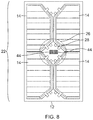
- FIG. 8 illustrates an example of the array 22 where one or more bypass diodes 44 are added to the exposed area 28 of the substrate 12 in the corner regions 26 , for use in one or more of the electrical connections.
- the bypass diodes 44 protect the solar cells 14 when the solar cells 14 become unable to generate current, which could be due to being partially shadowed, which drives the solar cells 14 into reverse bias.
- the bypass diodes 44 are attached to the substrate 12 in the corner regions 26 independent of the solar cells 14 .
- FIG. 9 illustrates an example where the bypass diode 44 is applied to the back side of the solar cell 14 , with an interconnect or contact 46 for the bypass diode 44 extending into the corner region 26 between the front and back contacts 32 , 34 .
- FIG. 10 illustrates a front side view of the example of FIG. 9 , with the interconnect or contact 46 for the bypass diode 44 (not shown) extending into the corner region 26 between the front and back contacts 32 , 34 .
- FIG. 11 illustrates the solar cells 14 of FIGS. 9 and 10 arranged into the 2D grid of the array 22 and applied to the substrate 12 , where the bypass diodes 44 (not shown) are applied to the back side of the solar cells 14 , with the contacts 46 for the bypass diodes 44 extending into the corner regions 26 of the solar cells 14 .
- FIGS. 7, 8 and 11 are generalized layouts. Specifically, these layouts can be repeated across any panel 10 a dimensions desired by a customer. This greatly simplifies assembly, rework, test, and inspection processes.
- Front and back contacts 32 , 34 of the solar cells 14 are present in each corner region 26 for attachment to the corner conductors 20 .
- Interconnects for the front and back contacts 32 , 34 of each of the solar cells 14 are welded, soldered, or otherwise bonded onto the corner conductors 20 to provide a conductive path 20 , 32 , 34 for routing power out of the solar cells 14 .
- Adjacent solar cells 14 can be electrically connected to flow current in up/down or left/right directions as desired by the specific design. Current flow can also be routed around stayout zones as needed.
- the length or width of the solar cell array 22 can be set as desired. Also, the width can vary over the length of the array 22 .
- the electrical connections are series connections that determine a flow of current through the plurality of solar cells 14 .
- This may be accomplished by the connection schemes shown in FIGS. 12 and 13 , wherein FIG. 12 shows up/down series connections 48 between the solar cells 14 of the array 22 , and FIG. 13 shows left/right series connections 50 between the solar cells 14 of the array 22 .
- these series connections 48 , 50 are electrical connections between the front contacts 32 and back contacts 34 of the solar cells 14 , and the bypass diodes 44 , are made using the corner conductors 20 formed on or in the exposed areas 28 of the substrate 12 .
- These series connections 48 , 50 determine the current (power) flow, as indicated by the arrows 52 , through the solar cells 14 , in contrast to the assembly of large strings off-substrate.
- the corner conductors 20 between solar cells 14 can be in many forms. They could be accomplished using wires that have electrical connections made on both ends, which could be from soldering, welding, conducting adhesive, or other process. In addition to wires, metal foil connectors, similar to the interconnects, could be applied. Metal conductive paths or traces (not shown) can also be integrated with the substrate 12 .
- this new approach attaches the solar cells 14 individually to a substrate 12 such that the corner regions 26 of two, three or four adjacent solar cells 14 are aligned on the substrate 12 .
- the solar cells 14 can be laid out so that the cropped corners 24 are aligned and the corner regions 26 are adjacent, thereby exposing an area 28 of the substrate 12 .
- Electrical connections between solar cells 14 are made in these corner regions 26 between front contacts 32 and back contacts 34 on the solar cells 14 , bypass diodes 44 , and corner conductors 20 on or in the exposed area 28 of the substrate 12 , wherein these conductive paths are used to create a string of solar cells 14 in a series connection 48 , 50 comprising a circuit.
- solder connections using solder are highly manufacturable; however, they are only sufficient for more mild space missions. Solder connections are highly manufacturable with low pressure and temperature, but solder is composed of small grains of alloys with different metal compositions and these alloys have low melting temperatures of ⁇ 300° C. Consequently, solder alloy phases and grains degrade through thermal cycles.
- Welding has become the industry standard for durability under these conditions.
- Welded connections can form solid, single phase metal connections using Ag/Ag joints that have superior performance through thermal cycles.
- the welding process requires stringent mechanical alignment of parts and high pressures of the welding tips which can lead to breakage.
- This disclosure identifies the value in using nano-metals to form the electrical connections on space-based solar arrays 22 .
- These nano-metals have the manufacturability of the solder, yet form the single composition of a high melting point material that gives welded connections their durability.
- FIGS. 14A-14F illustrate the advantages of a nano-metal contact formation.
- FIG. 14A shows a weld-based electrical connection before welding and FIG. 14B shows a weld-based electrical connection after welding, using two Ag metal pieces 54 a , 54 b .
- a roughness is drawn where the two Ag metal pieces 54 a , 54 b are brought into contact to emphasize the significance of mating the pieces on a microscopic level.
- the resistive weld tips 56 a , 56 b apply a large force on opposing sides bringing the pieces 54 a , 54 b together, wherein a pulse of current flows between the tips 56 a , 56 b .
- This current rapidly heats the metal of the pieces 54 a , 54 b and, with the applied force of the tips 56 a , 56 b , a solid Ag joint is formed by the pieces 54 a , 54 b that has excellent survival against thermal cycling.
- FIG. 14C shows a solder-based electrical connection before heating of the solder 58
- FIG. 14D shows a solder-based electrical connection after heating, using two Ag metal pieces 54 a , 54 b with a solder 58 positioned between the pieces 54 a , 54 b
- Many solders can be considered, which generally involve alloys of Indium (In), Tin (Sn) and/or Lead (Pb), which provide for a low melting point of 150-250° C.
- Ag is often added to the solder 58 , which controls reactions when soldering to Ag metal pieces 54 a , 54 b , as shown in this case.
- the solder 58 is based on mixture of at least two metals with a eutectic phase diagram.
- the eutectic is a metal composition that has a low melting point.
- the melted metal has a single composition.
- it solidifies with a eutectic transformation into two compositions that are highly different.
- a Sn/Pb solder 58 would solidify into a Sn-rich phase and a Pb-rich phase.
- the circles in FIGS. 14C and 14D are meant to indicate the grains with different phases.
- the composition is the same as the melt, but the composition is distributed differently in the solid.
- These phases have different melting points, creep rates, and different coefficients of thermal expansion. The phases thus respond differently to the thermal cycles, which leads to void formation between grains. These voids grow into cracks, which ultimately lead to failure.
- the low forces of the solder melt process and the low temperatures are desirable, but greater resistance to thermal cycling is needed as well.
- FIG. 14E shows a nano-metal based electrical connection before heating
- FIG. 14F shows a nano-metal based electrical connection after heating, using two Ag metal pieces 54 a , 54 b with a nano-metal material 60 positioned between the pieces 54 a , 54 b .
- the nano-metal material 60 is a nano-Ag material, for example, a paste or ink with nano-Ag particles that have sizes less than about 100 nm and possibly sizes in the range of about 0.5-10 nm.
- the small nano-Ag particles have a very high surface area, meaning many of the Ag atoms are unbonded. This lack of bonding is an instability. The Ag in these particles are unstable.
- the surface Ag atoms When brought into contact, the surface Ag atoms are unbonded and can move or rearrange. The result is high mobility of the Ag atoms at temperatures of 150-250° C., which is similar to melting. At these temperatures, the nano-Ag particles merge into a network. Lower temperatures ⁇ 180° C. and lower applied pressures ⁇ 1 MPa result in a porous network of solid, single phase Ag. Higher temperatures>200° C. and higher applied pressures>1 MPa result in a densification. This has been used for attaching integrated circuits to circuit boards and shown improved lifetime against thermal cycling as compared to solder.
- the nano-Ag material 60 is applied and processed similar to a solder 58 . Thus, it provides the manufacturing advantages of a solder 58 . After thermal processing, a solid Ag joint is formed between the Ag metal pieces 54 a , 54 b and the nano-Ag material 60 that is rugged against thermal cycles.
- FIG. 15 shows a side view of a solar cell 14 on a substrate 12 that is a flex sheet assembly, which is part of a solar cell array 22 on a solar cell panel 10 a , according to one example.
- the substrate 12 includes a polyimide base layer 62 with a Copper (Cu) layer 64 above it, wherein the Cu layer 64 is patterned into two corner conductors 20 .
- a polyimide top overlay 66 is positioned against the front surface of Cu layer 64 .
- the polyimide top overlay 66 has holes through to the two corner conductors 20 of the Cu layer 64 , which are subsequently plated with an Ag or Au surface layer 68 .
- a CIC unit comprising a solar cell 14 that is attached on its back side to the substrate 12 with adhesive 70 , a grid 36 on a front side (top) of the solar cell 14 , and a coverglass 72 attached to the grid 36 and front side of the solar cell 14 with adhesive 74 .
- the metal foil interconnects 76 attached to the nano-metal material 60 on top of the plated Ag or Au surface layers 68 on the corner conductors 20 of the Cu layer 64 of the substrate 12 and to the nano-metal material 60 on top of the contacts 32 , 34 on both the front and back sides of the solar cell 14 .
- the metal foil interconnects 76 may also connect to bypass diodes 44 (not shown).
- FIG. 15 also shows an electrical connection formed between first and second conductive elements by inserting a nano-metal material 60 between the first and second conductive elements; and then heating the nano-metal material 60 to a melting or solidification temperature forming a heated nano-metal material 60 , to form the electrical connection between the first and second conductive elements.
- the first and second conductive elements comprise: (1) the metal foil interconnects 76 and the plated Ag or Au surface layers 68 , as well as (2) the metal foil interconnects 76 and the front or back contacts 32 , 34 on the solar cell 14 .
- the nano-metal material 60 can be applied to any or all of the electrical connections used with a solar cell 14 and a substrate 12 on which the solar cell 14 is attached.
- the nano-metal material 60 is described above as a paste or ink comprised of one or more of Ag nano-particles, it is not limited to this material.
- the nano-metal material 60 comprises a nano-metal paste or ink comprised of one or more of Au, Cu, Ag, and/or Al nano-particles that melt or fuse into a solid, similar to a solder 58 , to form the electrical connection.
- the nano-metal material 60 particles have low melting temps, e.g., about 150-250 degrees C., and more preferably, about 175-225 degrees C.
- Ag may be preferred for the nano-metal material 60 , because Ag is often used for the metal foil interconnects 76 and grid 36 , as it is highly conductive and can be formed well into desired shapes, although Ag does tarnish and can erode in space environments with high atomic oxygen.
- Au can be preferred even with its higher cost or to use in an Au-coated Ag.
- Other alternatives include Cu or Al, which are substantially lower cost than Ag or Au. Any of these metals could be used for both the metal foil interconnects 76 and/or the nano-metal material 60 .
- the nano-metal material 60 is not an alloy. Alloy materials have different melting temps, which can be a problem with extreme thermal cycling.
- one case of mixed metals is a nano-metal material 60 comprised of a paste or ink with Au, Cu, Ag, and/or Al nano-particles that is placed between Ag pieces 54 a , 54 b .
- a nano-metal material 60 comprised of a paste or ink with Au, Cu, Ag, and/or Al nano-particles that is placed between Ag pieces 54 a , 54 b .
- This is a very different configuration than a solder connection that has numerous metal interfaces between micron size grains that have melting points less than about 400° C. Thus, creep, flow and failure of this interface is much less likely than the solder interface.
- This disclosure also describes how a solar cell 14 with back contacts 34 can be integrated with printed corner conductors 20 on a substrate 12 to form a solar cell array 22 that has no exposed metal. Specifically, through-holes are formed in the solar cell 14 , which are then plated or deposited with metal to create vias to connect front contacts 32 of the solar cell 14 to back contacts 34 of the solar cell 14 for connection to traces on the substrate 12 , using laser welding, soldering, or applying nano-metal pastes or other conducting adhesives.
- FIG. 16 also shows a side view of a solar cell 14 on a substrate 12 that is a flex sheet assembly, wherein the substrate 12 includes the polyimide base layer 62 with the Cu layer 64 above it.
- the polyimide top overlay 66 is positioned against the front surface of Cu layer 64 , which is plated with the Ag or Au surface layer 68 .
- Shown on the right side is the CIC unit comprising the solar cell 14 that is attached on its back side to the substrate 12 , the grid 36 on a front side (top) of the solar cell 14 , and the coverglass 72 attached to the grid 36 and front side of the solar cell 14 with adhesive 74 .
- the through-hole 82 is created through the semiconductor layers of the solar cell 14 between a front side and a back side of the solar cell 14 . Then, the sidewalls inside the through-hole 82 are passivated between the front and back sides of the solar cell 14 , and an insulating layer 84 is applied inside the through-hole 82 that extends through the through-hole 82 and wraps on portions of both the front and back surfaces of the solar cell 14 adjacent the through-hole 82 . A conductive layer 86 is deposited inside the through-hole 82 , and on portions of both the front and back surfaces of the solar cell 14 adjacent the through-hole 82 , resulting in the creation of a via 82 .
- the via 82 provides a conductive path from the front contact 32 on the front side of the solar cell 14 to the back side of the solar cell 14 .
- An electrical connection is then made between the conductive layer 86 on the back side of the solar cell 14 and the trace 78 formed in the Cu layer 64 of the substrate 12 , using solder 58 (or a nano-metal material 60 ) and the plated Ag or Au layer 68 , resulting in an electrical connection to the front contact 32 on the front side of the solar cell 14 .
- An electrical connection is also made between the back contact 34 of the solar cell 14 and the trace 80 formed in the Cu layer 64 of the substrate 12 , also using solder 58 (or a nano-metal material 60 ) and the plated Ag or Au layer 68 .
- this structure greatly minimizes any exposed metal in the solar cell array 22 . Moreover, this is accomplished in a highly manufacturable way, which avoids the manual efforts currently used.
- the via 82 also provides value to the performance of the solar cells 14 .
- the front side of the solar cell 14 is a balance of requiring sufficient metal to have a low resistance to bring the current to the wires or interconnects carrying electrical current off of the solar cell 14 . This is achieved by having long narrow lines in the grid 36 . Larger solar cells 14 have longer lines and higher current levels requiring ever greater amounts of metal to achieve low resistances. The addition of this metal, however, results in greater obscuration of the surface of the solar cell 14 , which reduces performance of the solar cell 14 .
- the via 82 of this disclosure completely changes this balance.
- the current from all the lines of the grid 36 was extracted to a wide bus bar on one side of the solar cell 14 and then to two or three interconnects.
- the current on the front side of the solar cell 14 has a shorter path to travel, to more connection points, and less metal is needed.
- FIG. 17 shows how traces 78 , 80 in the Cu layer 64 of the substrate 12 under the solar cell 14 could be laid out to extract current from the front and back contacts 32 , 34 .
- the electrical current collected by the grid 36 flows to the front contact 32 (as shown in FIG. 5 ).
- the current then flows from the front contact 32 along trace 88 to the via 82 , and through the via 82 to the back side of the solar cell 14 .
- the conductive layer 86 around the via 82 on the back side of the solar cell 14 contacts the trace 78 on the substrate 12 (as shown in FIG. 16 ).
- an electrical connection is made between the back contact 34 of the solar cell 14 and the trace 80 .
- the traces 78 , 80 are highly conductive paths buried in the substrate 12 , and insulated from the solar cell 14 , that do not block any sunlight.
- the dashed lines of the traces 80 indicate that they are hidden underneath the solar cells 14 (with traces 78 also hidden underneath the solar cells 14 and traces 88 ).
- the fingers 38 of the grid 36 could be made shorter, for example, in a configuration with more vias 82 .
- the conductive vias 82 also enable both the resistance and the obscuration to be reduced, which before were opposing goals.
- a conductive via 82 is well known. What is significant about this disclosure, however, is how these vias 82 can be coupled with corner conductors 20 in the substrate 12 to extract power.
- welding is preferred for its ruggedness in the thermal cycle environment of space and for many missions required.
- a resistive weld could be hard to accomplish in this design.
- a substrate 12 comprising a flex sheet assembly would most likely use polyimide, which strongly absorbs blue/UV light, giving it an orange appearance. It may be possible to use a red or near infrared laser for welding or to use a more transparent polymer. If possible to be formed, this could be a rugged connection suitable for the space environment.
- soldering would be highly desirable and straightforward.
- Solder 58 preforms or paste could be added to one or both of the solar cell 14 and the substrate 12 electrical connections. These can be brought together, possibly with pressure, and heated to reflow the solder 58 . This would be similar to circuit board assembly on a very large scale. Solder 58 , however, is known to only be suitable for short space missions.
- the nano-metal material 60 may be comprised of a paste or ink with one or more of Au, Cu, Ag, and/or Al nano-particles that melt or fuse into a solid, similar to a solder 58 , to form the electrical connection.
- the nano-metal material 60 particles have low melting temps, e.g., about 150-250 degrees C., and more preferably, about 175-225 degrees C.
- nano-metal materials 60 could be very advantageous using a process similar to the process flow of solder 58 , where the paste is dispensed, the pieces brought together, and heated.
- a solid single-phase metal connection using the nano-metal material 60 may have advantages to solder 58 .
- Examples of the disclosure may be described in the context of a method 90 of fabricating a solar cell 14 , solar cell panel 10 a and/or satellite, comprising steps 92 - 104 , as shown in FIG. 18 , wherein the resulting satellite 106 having a solar cell panel 10 a comprised of solar cells 14 are shown in FIG. 19 .
- exemplary method 90 may include specification and design 92 of the solar cell 14 , solar cell panel 10 a and/or satellite 106 , and material procurement 94 for same.
- solar cell panel 10 a and/or satellite 106 takes place, which include fabricating the solar cell 14 , solar cell panel 10 a and/or satellite 106 .
- the solar cell 14 , solar cell panel 10 a and/or satellite 106 may go through certification and delivery 100 in order to be placed in service 102 .
- the solar cell 14 , solar cell panel 10 a and/or satellite 106 may also be scheduled for maintenance and service 104 (which includes modification, reconfiguration, refurbishment, and so on), before being launched.
- a system integrator may include without limitation any number of solar cell, solar cell panel, satellite or spacecraft manufacturers and major-system subcontractors;
- a third party may include without limitation any number of venders, subcontractors, and suppliers; and
- an operator may be a satellite company, military entity, service organization, and so on.
- a satellite 106 fabricated by exemplary method 90 may include systems 108 , a body 110 , solar cell panels 10 a comprised of solar cells 14 , and one or more antennae 112 .
- the systems 108 included with the satellite 106 include, but are not limited to, one or more of a propulsion system 114 , an electrical system 116 , a communications system 118 , and a power system 120 . Any number of other systems 108 also may be included.
- FIG. 20 is an illustration of the solar cell panel 10 a in the form of a functional block diagram, according to one example.
- the solar cell panel 10 a is comprised of the solar cell array 22 , which is comprised of one or more of the solar cells 14 individually attached to the substrate 12 .
- Each of the solar cells 14 absorbs light 122 from a light source 124 and generates an electrical output 126 in response thereto.
- At least one of the solar cells 14 has at least one cropped corner 24 that defines a corner region 26 , such that an area 28 of the substrate 12 remains exposed when the solar cell 14 is attached to the substrate 12 .
- the corner regions 26 of adjacent ones of the solar cells 14 are aligned, thereby exposing the area 28 of the substrate 12 .
- the area 28 of the substrate 12 that remains exposed includes one or more corner conductors 20 attached to, printed on, or integrated with the substrate 12 , and one or more electrical connections between the solar cells 14 and the corner conductors 20 are made in a corner region 26 .
- the corner region 26 may also include one or more bypass diodes 44 .
- the corner region 26 includes at least one contact, for example, a front contact 32 on a front side of the solar cell 14 and/or a back contact 34 on a back side of the solar cell 14 .
- the solar cell 14 may include a via 82 extending between a front side and a back side of the solar cell 14 , wherein the via 82 provides a conductive path from the front contact 32 on the front side of the solar cell 14 to the back side of the solar cell 14 .
- An electrical connection is then made between the via 82 on the back side of the solar cell 14 and the trace 78 formed in the substrate 12 , using solder 58 or a nano-metal material 60 , resulting in an electrical connection to the front contact 32 on the front side of the solar cell 14 .
- An electrical connection is also made between the back contact 34 of the solar cell 14 and the trace 80 formed in the substrate 12 , also using solder 58 or a nano-metal material 60 . Because the traces 78 , 80 are buried in the substrate 12 , this structure greatly minimizes any exposed metal in the solar cell array 22 .
Landscapes
- Engineering & Computer Science (AREA)
- Physics & Mathematics (AREA)
- Power Engineering (AREA)
- Computer Hardware Design (AREA)
- Microelectronics & Electronic Packaging (AREA)
- Condensed Matter Physics & Semiconductors (AREA)
- General Physics & Mathematics (AREA)
- Electromagnetism (AREA)
- Life Sciences & Earth Sciences (AREA)
- Sustainable Development (AREA)
- Sustainable Energy (AREA)
- Chemical & Material Sciences (AREA)
- Crystallography & Structural Chemistry (AREA)
- Manufacturing & Machinery (AREA)
- Materials Engineering (AREA)
- Nanotechnology (AREA)
- Photovoltaic Devices (AREA)
Priority Applications (31)
| Application Number | Priority Date | Filing Date | Title |
|---|---|---|---|
| US15/643,289 US11437533B2 (en) | 2016-09-14 | 2017-07-06 | Solar cells for a solar cell array |
| US15/643,287 US10763383B2 (en) | 2016-09-14 | 2017-07-06 | Nano-metal connections for a solar cell array |
| ES17191166T ES2970380T3 (es) | 2016-09-14 | 2017-09-14 | Conexiones nanometálicas para un conjunto de celdas solares |
| EP17191134.0A EP3297032B1 (fr) | 2016-09-14 | 2017-09-14 | Conducteurs préfabriqués sur un substrat pour faciliter des connexions d'angle pour un réseau de cellules solaires |
| JP2017176668A JP7455496B2 (ja) | 2016-09-14 | 2017-09-14 | ソーラーセルアレイ内の構成要素の改修及び修理 |
| EP17191154.8A EP3297033A1 (fr) | 2016-09-14 | 2017-09-14 | Recyclage et réparation de composants dans un réseau de piles solaires |
| EP17191168.8A EP3297035B1 (fr) | 2016-09-14 | 2017-09-14 | Connexions de réseau de cellules solaires au moyen de conducteurs d'angle |
| JP2017176670A JP7475804B2 (ja) | 2016-09-14 | 2017-09-14 | ソーラーセルアレイ用の電力ルーティングモジュール |
| EP23169034.8A EP4235815A3 (fr) | 2016-09-14 | 2017-09-14 | Conducteurs préfabriqués sur un substrat pour faciliter des connexions d'angle pour un réseau de cellules solaires |
| JP2017176672A JP7411320B2 (ja) | 2016-09-14 | 2017-09-14 | ソーラーセルアレイ用のナノ金属接続 |
| EP21174069.1A EP3907766A1 (fr) | 2016-09-14 | 2017-09-14 | Connexions de réseau de cellules solaires au moyen de conducteurs d'angle |
| EP17191166.2A EP3297034B1 (fr) | 2016-09-14 | 2017-09-14 | Connexions nano-métalliques pour réseau de cellules solaires |
| EP17191159.7A EP3297041B1 (fr) | 2016-09-14 | 2017-09-14 | Module d'acheminement de puissance pour un réseau de cellules solaires |
| JP2017176673A JP7171175B2 (ja) | 2016-09-14 | 2017-09-14 | ソーラーセルアレイ用のソーラーセル |
| JP2017176669A JP2018078277A (ja) | 2016-09-14 | 2017-09-14 | ソーラーセルアレイのためのスイッチングマトリックスを有する電力ルーティングモジュール |
| JP2017176671A JP7475805B2 (ja) | 2016-09-14 | 2017-09-14 | コーナー導体を使用するソーラーセルアレイ接続 |
| EP23178386.1A EP4235810A3 (fr) | 2016-09-14 | 2017-09-14 | Recyclage et réparation de composants dans un réseau de piles solaires |
| EP17191162.1A EP3297042B1 (fr) | 2016-09-14 | 2017-09-14 | Module d'acheminement de puissance avec une matrice de commutation pour un réseau de cellules solaires |
| EP23197851.1A EP4273940A3 (fr) | 2016-09-14 | 2017-09-14 | Module d'acheminement de puissance pour un réseau de cellules solaires |
| JP2017176667A JP7295612B2 (ja) | 2016-09-14 | 2017-09-14 | ソーラーセルアレイためのコーナー接続を促進するための、基板上のあらかじめ製作された導体 |
| US15/787,291 US20180358497A1 (en) | 2017-06-12 | 2017-10-18 | Solar cell array with changeable string length |
| US15/787,304 US20180358491A1 (en) | 2017-06-12 | 2017-10-18 | Solar cell array with bypassed solar cells |
| JP2018109912A JP2019050351A (ja) | 2017-06-12 | 2018-06-08 | 迂回させたソーラーセルを有するソーラーセルアレイ |
| JP2018109908A JP2019050350A (ja) | 2017-06-12 | 2018-06-08 | 変更可能なストリング長を有するソーラーセルアレイ |
| US16/991,589 US20200373446A1 (en) | 2016-09-14 | 2020-08-12 | Nano-metal connections for a solar cell array |
| JP2022152000A JP2022188130A (ja) | 2016-09-14 | 2022-09-22 | ソーラーセルアレイ用の電力ルーティングモジュール |
| JP2022151999A JP2022188129A (ja) | 2016-09-14 | 2022-09-22 | ソーラーセルアレイのためのスイッチングマトリックスを有する電力ルーティングモジュール |
| JP2022157012A JP2023002572A (ja) | 2016-09-14 | 2022-09-29 | コーナー導体を使用するソーラーセルアレイ接続 |
| JP2022162406A JP2023002612A (ja) | 2016-09-14 | 2022-10-07 | ソーラーセルアレイ内の構成要素の改修及び修理 |
| JP2022176602A JP2023022029A (ja) | 2016-09-14 | 2022-11-02 | ソーラーセルアレイ用のソーラーセル |
| JP2023137305A JP2023169172A (ja) | 2017-06-12 | 2023-08-25 | 迂回させたソーラーセルを有するソーラーセルアレイ |
Applications Claiming Priority (13)
| Application Number | Priority Date | Filing Date | Title |
|---|---|---|---|
| US201662394636P | 2016-09-14 | 2016-09-14 | |
| US201662394616P | 2016-09-14 | 2016-09-14 | |
| US201662394629P | 2016-09-14 | 2016-09-14 | |
| US201662394666P | 2016-09-14 | 2016-09-14 | |
| US201662394623P | 2016-09-14 | 2016-09-14 | |
| US201662394641P | 2016-09-14 | 2016-09-14 | |
| US201662394649P | 2016-09-14 | 2016-09-14 | |
| US201662394671P | 2016-09-14 | 2016-09-14 | |
| US201662394672P | 2016-09-14 | 2016-09-14 | |
| US201662394627P | 2016-09-14 | 2016-09-14 | |
| US201662394632P | 2016-09-14 | 2016-09-14 | |
| US201662394667P | 2016-09-14 | 2016-09-14 | |
| US15/643,287 US10763383B2 (en) | 2016-09-14 | 2017-07-06 | Nano-metal connections for a solar cell array |
Related Parent Applications (2)
| Application Number | Title | Priority Date | Filing Date |
|---|---|---|---|
| US15/643,274 Continuation-In-Part US20180076346A1 (en) | 2016-09-14 | 2017-07-06 | Solar cell array connections using corner conductors |
| US15/643,289 Continuation-In-Part US11437533B2 (en) | 2016-09-14 | 2017-07-06 | Solar cells for a solar cell array |
Related Child Applications (2)
| Application Number | Title | Priority Date | Filing Date |
|---|---|---|---|
| US15/643,285 Continuation-In-Part US20180076761A1 (en) | 2016-09-14 | 2017-07-06 | Power routing module with a switching matrix for a solar cell array |
| US16/991,589 Division US20200373446A1 (en) | 2016-09-14 | 2020-08-12 | Nano-metal connections for a solar cell array |
Publications (2)
| Publication Number | Publication Date |
|---|---|
| US20180076344A1 US20180076344A1 (en) | 2018-03-15 |
| US10763383B2 true US10763383B2 (en) | 2020-09-01 |
Family
ID=62149305
Family Applications (3)
| Application Number | Title | Priority Date | Filing Date |
|---|---|---|---|
| US15/643,287 Active 2037-09-09 US10763383B2 (en) | 2016-09-14 | 2017-07-06 | Nano-metal connections for a solar cell array |
| US15/643,289 Active US11437533B2 (en) | 2016-09-14 | 2017-07-06 | Solar cells for a solar cell array |
| US16/991,589 Pending US20200373446A1 (en) | 2016-09-14 | 2020-08-12 | Nano-metal connections for a solar cell array |
Family Applications After (2)
| Application Number | Title | Priority Date | Filing Date |
|---|---|---|---|
| US15/643,289 Active US11437533B2 (en) | 2016-09-14 | 2017-07-06 | Solar cells for a solar cell array |
| US16/991,589 Pending US20200373446A1 (en) | 2016-09-14 | 2020-08-12 | Nano-metal connections for a solar cell array |
Country Status (4)
| Country | Link |
|---|---|
| US (3) | US10763383B2 (fr) |
| EP (3) | EP4235810A3 (fr) |
| JP (12) | JP7475804B2 (fr) |
| ES (1) | ES2970380T3 (fr) |
Cited By (2)
| Publication number | Priority date | Publication date | Assignee | Title |
|---|---|---|---|---|
| USD913210S1 (en) * | 2014-10-15 | 2021-03-16 | Sunpower Corporation | Solar panel |
| USD999723S1 (en) | 2014-10-15 | 2023-09-26 | Sunpower Corporation | Solar panel |
Families Citing this family (3)
| Publication number | Priority date | Publication date | Assignee | Title |
|---|---|---|---|---|
| KR20200114055A (ko) * | 2019-03-27 | 2020-10-07 | 주식회사 엘지화학 | 투명 발광소자 디스플레이 |
| US11722094B2 (en) * | 2020-08-21 | 2023-08-08 | The Boeing Company | Flexible circuit for solar cell assemblies |
| CN116632118B (zh) * | 2023-07-18 | 2023-09-26 | 英利能源发展有限公司 | 光伏组件的制备方法 |
Citations (52)
| Publication number | Priority date | Publication date | Assignee | Title |
|---|---|---|---|---|
| DE1013644B (de) | 1955-01-14 | 1957-08-14 | Stamicarbon | Verfahren zur Herstellung grobkoernigen Harnstoffs |
| US4257821A (en) | 1978-11-13 | 1981-03-24 | Trw Inc. | Universal solar cell/conductor junction element and solar panel embodying same |
| US4481378A (en) | 1982-07-30 | 1984-11-06 | Motorola, Inc. | Protected photovoltaic module |
| US4755231A (en) | 1986-06-13 | 1988-07-05 | Trw Inc. | Flexible solar array cell and substrate therefor |
| US5391235A (en) | 1992-03-31 | 1995-02-21 | Canon Kabushiki Kaisha | Solar cell module and method of manufacturing the same |
| US5567248A (en) | 1995-09-05 | 1996-10-22 | Chung; Darius | Modular solar cell contact arrangement |
| US5701067A (en) | 1995-02-24 | 1997-12-23 | Sanyo Electric Co., Ltd. | Battery charger and solar cells for battery charging |
| US6034322A (en) | 1999-07-01 | 2000-03-07 | Space Systems/Loral, Inc. | Solar cell assembly |
| US6156967A (en) | 1998-06-04 | 2000-12-05 | Tecstar Power Systems, Inc. | Modular glass covered solar cell array |
| US6313396B1 (en) | 2000-05-22 | 2001-11-06 | The Boeing Company | Lightweight solar module and method of fabrication |
| EP1160876A2 (fr) | 2000-05-30 | 2001-12-05 | The Boeing Company | Matrice reconfigurable de panneaux solaires |
| US6441297B1 (en) | 1998-03-13 | 2002-08-27 | Steffen Keller | Solar cell arrangement |
| DE10136442A1 (de) | 2001-07-26 | 2003-02-13 | Ralf Adelhelm | Kontakte und Verbinder von Solarzellen |
| US6555739B2 (en) | 2001-09-10 | 2003-04-29 | Ekla-Tek, Llc | Photovoltaic array and method of manufacturing same |
| US6563289B1 (en) | 1998-09-04 | 2003-05-13 | Eev Limited | Solar cell arrangements |
| EP1548847A2 (fr) | 2003-12-23 | 2005-06-29 | Alcatel | Panneau de générateur solaire et satellite associé |
| US20070152194A1 (en) * | 2005-12-30 | 2007-07-05 | Intel Corporation | Nano-scale particle paste for wiring microelectronic devices using deposition and ink-jet printing |
| US20080142071A1 (en) | 2006-12-15 | 2008-06-19 | Miasole | Protovoltaic module utilizing a flex circuit for reconfiguration |
| US20080245405A1 (en) | 2005-03-11 | 2008-10-09 | Bp Corporation North America Inc. | Integrated Solar Cell Roofing System and Method of Manufacture |
| US20080295889A1 (en) | 2007-05-07 | 2008-12-04 | Leonhard Kurz Stiftung & Co. Kg | Photovoltaic Module |
| WO2009012567A1 (fr) | 2007-07-23 | 2009-01-29 | Day4 Energy Inc. | Protection d'ombre pour cellules solaires et modules de cellules solaires |
| US20090272436A1 (en) | 2008-05-05 | 2009-11-05 | Osbert Hay Cheung | Non-glass photovoltaic module and methods for manufacture |
| US20090288702A1 (en) | 2008-05-22 | 2009-11-26 | Kim Yun-Gi | Solar Cell and Solar Cell Module Using the Same |
| US20100186795A1 (en) | 2009-01-28 | 2010-07-29 | Stephen Joseph Gaul | Connection systems and methods for solar cells |
| US20100295383A1 (en) | 2009-05-19 | 2010-11-25 | Coolearth Solar | Architecture for power plant comprising clusters of power-generation devices |
| US20100313954A1 (en) | 2009-06-16 | 2010-12-16 | Emcore Solar Power, Inc. | Concentrated Photovoltaic System Receiver for III-V Semiconductor Solar Cells |
| US20110079263A1 (en) | 2009-10-02 | 2011-04-07 | Tigo Energy, Inc. | Systems and Methods to Provide Enhanced Diode Bypass Paths |
| US20110120752A1 (en) | 2009-11-20 | 2011-05-26 | Hitachi Cable, Ltd. | Method for fabricating a solar battery module and a wiring substrate for a solar battery |
| US20110138609A1 (en) | 2009-12-16 | 2011-06-16 | Nagendra Srinivas Cherukupalli | Systems, Circuits, and Methods for an Adaptive Solar Power System |
| US20120125391A1 (en) * | 2010-11-19 | 2012-05-24 | Solopower, Inc. | Methods for interconnecting photovoltaic cells |
| US20120167954A1 (en) | 2009-07-22 | 2012-07-05 | Applied Materials, Inc. | Monolithic module assembly using back contact solar cells and metal ribbon |
| US20120313455A1 (en) | 2011-06-08 | 2012-12-13 | Latham Andrew V | Instantaneous solar array recombining technology |
| US20130014802A1 (en) | 2011-07-12 | 2013-01-17 | Astrium Gmbh | Solar cell and solar cell assembly |
| US8604330B1 (en) | 2010-12-06 | 2013-12-10 | 4Power, Llc | High-efficiency solar-cell arrays with integrated devices and methods for forming them |
| US20140000682A1 (en) | 2012-06-27 | 2014-01-02 | E I Du Pont De Nemours And Company | Integrated back-sheet for back contact photovoltaic module |
| US20140033625A1 (en) | 2012-06-12 | 2014-02-06 | Certainteed Corporation | Photovoltaic Roofing Systems With Inner Corner Flashings |
| US20140366927A1 (en) | 2012-01-23 | 2014-12-18 | Stc.Unm | Multi-source optimal reconfigurable energy harvester |
| EP2833416A1 (fr) | 2012-03-30 | 2015-02-04 | Toppan Printing Co., Ltd. | Module de cellules solaires type à contact arrière |
| CN104443439A (zh) | 2014-11-18 | 2015-03-25 | 上海空间电源研究所 | 一种折叠展开式电池内置的柔性太阳电池阵 |
| US20150144173A1 (en) | 2013-11-27 | 2015-05-28 | Space Systems/Loral, Llc | Integral corner bypass diode interconnecting configuration for multiple solar cells |
| US20150318420A1 (en) * | 2014-04-30 | 2015-11-05 | Richard Hamilton SEWELL | Bonds for solar cell metallization |
| US20150349703A1 (en) | 2014-05-27 | 2015-12-03 | Cogenra Solar, Inc. | Shingled solar cell module |
| EP2981156A1 (fr) | 2014-07-29 | 2016-02-03 | Bubendorff | Panneau photovoltaïque et un procédé de fabrication d'un tel panneau |
| US20160126380A1 (en) | 2014-10-30 | 2016-05-05 | Sung Un CHANG | Flexible solar panel and method of fabricating the same |
| US20160197207A1 (en) | 2014-12-09 | 2016-07-07 | Mitsubishi Electric Corporation | Solar cell, solar cell module, and manufacturing method of solar cell |
| US20160218665A1 (en) | 2015-01-22 | 2016-07-28 | Solaero Technologies Corp. | Space solar cell panel with blocking diodes |
| US20160380221A1 (en) | 2014-09-05 | 2016-12-29 | Kabushiki Kaisha Toshiba | Photoelectric conversion element, wiring board for photoelectric conversion element, method for manufacturing photoelectric conversion element and photoelectric conversion structure |
| US20170018670A1 (en) | 2014-04-02 | 2017-01-19 | Stichting Energieonderzoek Centrum Nederland | Photovoltaic module with bypass diodes |
| US20170163212A1 (en) | 2015-12-08 | 2017-06-08 | Alta Devices, Inc. | Versatile flexible circuit interconnection for flexible solar cells |
| US9758261B1 (en) | 2015-01-15 | 2017-09-12 | Solaero Technologies Corp. | Inverted metamorphic multijunction solar cell with lightweight laminate substrate |
| EP3297042A1 (fr) | 2016-09-14 | 2018-03-21 | The Boeing Company | Module d'acheminement de puissance avec une matrice de commutation pour un réseau de cellules solaires |
| US20190127089A1 (en) | 2016-05-11 | 2019-05-02 | Mitsubishi Electric Corporation | Solar power generator, solar array wing, and space structure |
Family Cites Families (67)
| Publication number | Priority date | Publication date | Assignee | Title |
|---|---|---|---|---|
| JPS6167966A (ja) * | 1984-09-11 | 1986-04-08 | Sharp Corp | 太陽電池アレイ |
| JPS61202474A (ja) * | 1985-03-05 | 1986-09-08 | Mitsubishi Electric Corp | 宇宙用太陽電池アレイ |
| JPH0711475Y2 (ja) * | 1988-09-30 | 1995-03-15 | 日本電気株式会社 | 太陽電池セル |
| JPH04223378A (ja) * | 1990-12-25 | 1992-08-13 | Sharp Corp | 太陽電池 |
| JP2912496B2 (ja) | 1991-09-30 | 1999-06-28 | シャープ株式会社 | 太陽電池モジュール |
| JP3602721B2 (ja) * | 1998-06-12 | 2004-12-15 | 株式会社豊田自動織機 | 太陽電池モジュール |
| JP2000012885A (ja) * | 1998-06-23 | 2000-01-14 | Honda Motor Co Ltd | 太陽電池 |
| US6008448A (en) | 1998-10-15 | 1999-12-28 | Space Systems/Loral, Inc. | Solar panel array with stepped taper |
| JP3748344B2 (ja) * | 1999-10-12 | 2006-02-22 | ミサワホーム株式会社 | 太陽電池パネル |
| JP2002190612A (ja) | 2000-12-22 | 2002-07-05 | Mitsubishi Electric Corp | ソーラーアレイパネルおよびその製造方法 |
| ITMI20011653A1 (it) * | 2001-07-30 | 2003-01-30 | Lorenzo Cerofolini | Dispositivo di alimentazione elettrica a celle solari |
| US6637702B1 (en) | 2002-04-24 | 2003-10-28 | Lockheed Martin Corporation | Nested beam deployable solar array |
| JP2004241753A (ja) | 2002-12-13 | 2004-08-26 | Canon Inc | 太陽電池モジュール |
| JP3873889B2 (ja) | 2003-01-16 | 2007-01-31 | 株式会社デンソー | ワイヤボンディング方法 |
| DE102004044061A1 (de) * | 2004-09-11 | 2006-04-20 | Rwe Space Solar Power Gmbh | Solarzellenanordung sowie Verfahren zum Verschalten eines Solarzellenstrings |
| US7245134B2 (en) | 2005-01-31 | 2007-07-17 | Formfactor, Inc. | Probe card assembly including a programmable device to selectively route signals from channels of a test system controller to probes |
| KR100735395B1 (ko) | 2005-05-10 | 2007-07-04 | 삼성전자주식회사 | 집적 회로를 이용한 인쇄회로기판의 라우팅 방법 |
| US20140166067A1 (en) | 2006-08-07 | 2014-06-19 | Emcore Solar Power, Inc. | Solar power system for aircraft, watercraft, or land vehicles using inverted metamorphic multijunction solar cells |
| DE102007011403A1 (de) | 2007-03-08 | 2008-09-11 | Fraunhofer-Gesellschaft zur Förderung der angewandten Forschung e.V. | Frontseitig serienverschaltetes Solarmodul |
| JP2008282926A (ja) | 2007-05-09 | 2008-11-20 | Sanyo Electric Co Ltd | 太陽電池モジュール |
| WO2009067526A2 (fr) * | 2007-11-19 | 2009-05-28 | Sheats James R | Cellule solaire à haut rendement et haut courant et module solaire |
| US8933320B2 (en) | 2008-01-18 | 2015-01-13 | Tenksolar, Inc. | Redundant electrical architecture for photovoltaic modules |
| US20090255571A1 (en) | 2008-04-14 | 2009-10-15 | Bp Corporation North America Inc. | Thermal Conducting Materials for Solar Panel Components |
| US20100012172A1 (en) | 2008-04-29 | 2010-01-21 | Advent Solar, Inc. | Photovoltaic Modules Manufactured Using Monolithic Module Assembly Techniques |
| CN201369335Y (zh) * | 2008-10-15 | 2009-12-23 | 太聚能源股份有限公司 | 光伏电池模块 |
| JP5064353B2 (ja) | 2008-10-27 | 2012-10-31 | シャープ株式会社 | 太陽電池装置、携帯電子機器、並びに全地球測位システム装置 |
| US20110168238A1 (en) | 2010-01-11 | 2011-07-14 | Solopower, Inc. | Flexible solar modules and manufacturing the same |
| TW201032339A (en) * | 2009-02-20 | 2010-09-01 | Aussmak Optoelectronic Corp | Solar cell |
| JP4915821B2 (ja) * | 2009-03-17 | 2012-04-11 | 独立行政法人産業技術総合研究所 | 太陽光発電システム |
| JP2011071214A (ja) | 2009-09-24 | 2011-04-07 | Kaneka Corp | 太陽電池モジュール |
| US20110073163A1 (en) | 2009-09-25 | 2011-03-31 | Osbert Hay Cheung | Photovoltaic lamination and roof mounting systems |
| JP5459766B2 (ja) * | 2009-10-01 | 2014-04-02 | Nec東芝スペースシステム株式会社 | 太陽電池パネル、太陽電池パネルの帯電抑制方法及び人工衛星搭載用太陽光発電装置 |
| JP2011155041A (ja) | 2010-01-26 | 2011-08-11 | Kyocera Corp | 太陽電池素子および太陽電池モジュール |
| US8469313B2 (en) | 2010-02-16 | 2013-06-25 | The Boeing Company | Aerodynamic structure having a ridged solar panel and an associated method |
| KR100965541B1 (ko) * | 2010-02-17 | 2010-06-23 | 아익시스코리아(주) | 태양전지 모듈 및 그 제조방법 |
| JP2011210747A (ja) | 2010-03-26 | 2011-10-20 | Mitsubishi Chemicals Corp | 太陽電池モジュール及びその製造方法 |
| TWI604624B (zh) | 2010-05-11 | 2017-11-01 | 荷蘭能源研究基金會 | 太陽能電池與其製備方法 |
| JP2012043981A (ja) * | 2010-08-19 | 2012-03-01 | National Institute Of Advanced Industrial & Technology | 太陽電池モジュール |
| NL2005261C2 (en) * | 2010-08-24 | 2012-02-27 | Solland Solar Cells B V | Back contacted photovoltaic cell with an improved shunt resistance. |
| US8814099B1 (en) | 2010-08-31 | 2014-08-26 | MMA Design, LLC | Deployable morphing modular solar array |
| KR101091264B1 (ko) * | 2010-09-10 | 2011-12-07 | 주식회사 디엠에스 | 염료 감응형 태양전지 모듈 |
| WO2012058053A2 (fr) | 2010-10-29 | 2012-05-03 | Applied Materials, Inc. | Ensemble module monolithique utilisant des cellules solaires à contact arrière et du ruban métallique |
| JP2012138518A (ja) | 2010-12-27 | 2012-07-19 | Sony Corp | 太陽光発電モジュールおよび検査方法 |
| KR20120091670A (ko) | 2011-02-09 | 2012-08-20 | 엘지전자 주식회사 | 태양전지 모듈 및 그 제조방법 |
| JP2012204651A (ja) * | 2011-03-25 | 2012-10-22 | Sharp Corp | 太陽電池モジュール、太陽光発電システム、太陽電池モジュールにおける太陽電池セルの接続切替制御方法、接続切替制御プログラム、及び記録媒体 |
| AT12996U1 (de) | 2011-06-07 | 2013-03-15 | Austria Tech & System Tech | Photovoltaisches modul und verwendung desselben |
| NL1038916C2 (en) | 2011-07-01 | 2013-01-07 | Stichting Energie | Photovoltaic cell with wrap through connections. |
| WO2013031297A1 (fr) * | 2011-08-31 | 2013-03-07 | 三洋電機株式会社 | Procédé de fabrication de module de piles solaires |
| US20130056047A1 (en) | 2011-09-02 | 2013-03-07 | Markus E. Beck | Photovoltaic module with sealed perimeter and method of formation |
| JP2013080788A (ja) * | 2011-10-03 | 2013-05-02 | Sharp Corp | 太陽電池モジュール |
| JP2013175624A (ja) | 2012-02-27 | 2013-09-05 | Hitachi High-Technologies Corp | 太陽電池モジュールの生産方法および太陽電池モジュール組立装置 |
| US9120583B1 (en) | 2012-03-01 | 2015-09-01 | Deployable Space Systems, Inc. | Space solar array architecture for ultra-high power applications |
| GB2501899A (en) | 2012-05-09 | 2013-11-13 | Itouchenergy Ltd | Solar cell module and systems |
| US9356173B2 (en) * | 2012-08-31 | 2016-05-31 | Sandia Corporation | Dynamically reconfigurable photovoltaic system |
| JP2014049724A (ja) * | 2012-09-04 | 2014-03-17 | Sharp Corp | 太陽電池モジュール |
| DE102012217105A1 (de) * | 2012-09-24 | 2014-04-17 | Robert Bosch Gmbh | Elektrische Schaltung und Verfahren zum Herstellen einer elektrischen Schaltung |
| WO2014138242A1 (fr) | 2013-03-05 | 2014-09-12 | Sion Power Corporation | Cellules électrochimiques comprenant des matériaux en fibrille, tels que matériaux de cellulose en fibrille |
| CN203277428U (zh) | 2013-04-12 | 2013-11-06 | 北京桑纳斯太阳能电池有限公司 | Pcb背板的太阳能电池组件 |
| TWM512217U (zh) * | 2013-06-20 | 2015-11-11 | Plant PV | 太陽能電池 |
| US11302987B2 (en) | 2014-10-16 | 2022-04-12 | Lat Enterprises | Material for dissipating heat from and/or reducing heat signature of electronic devices and clothing |
| JP2015207598A (ja) * | 2014-04-17 | 2015-11-19 | 三菱電機株式会社 | 太陽電池モジュール、太陽電池およびこれに用いられる素子間接続体 |
| CN204558477U (zh) * | 2015-05-05 | 2015-08-12 | 中国人民解放军军械工程学院 | 表面具有互联网格状抗静电膜的太阳能电池及其组件 |
| KR20170012123A (ko) | 2015-07-24 | 2017-02-02 | 주식회사 엘지화학 | 가요성 기판의 제조방법 |
| US20170040933A1 (en) | 2015-08-03 | 2017-02-09 | Grid+ Advisors, LLC | Photovoltiac nanogrid systems |
| US10097005B2 (en) | 2015-08-17 | 2018-10-09 | Solarcity Corporation | Self-configuring photo-voltaic panels |
| KR102391513B1 (ko) | 2015-10-05 | 2022-04-27 | 삼성전자주식회사 | 물질막 적층체, 발광 소자, 발광 패키지, 및 발광 소자의 제조 방법 |
| CN109075737B (zh) | 2016-05-17 | 2022-07-12 | 日本瑞翁株式会社 | 发电模块连结体、光电转换模块连结体及发电装置 |
-
2017
- 2017-07-06 US US15/643,287 patent/US10763383B2/en active Active
- 2017-07-06 US US15/643,289 patent/US11437533B2/en active Active
- 2017-09-14 JP JP2017176670A patent/JP7475804B2/ja active Active
- 2017-09-14 EP EP23178386.1A patent/EP4235810A3/fr active Pending
- 2017-09-14 JP JP2017176667A patent/JP7295612B2/ja active Active
- 2017-09-14 EP EP23169034.8A patent/EP4235815A3/fr active Pending
- 2017-09-14 EP EP23197851.1A patent/EP4273940A3/fr active Pending
- 2017-09-14 JP JP2017176671A patent/JP7475805B2/ja active Active
- 2017-09-14 JP JP2017176673A patent/JP7171175B2/ja active Active
- 2017-09-14 ES ES17191166T patent/ES2970380T3/es active Active
- 2017-09-14 JP JP2017176669A patent/JP2018078277A/ja active Pending
- 2017-09-14 JP JP2017176672A patent/JP7411320B2/ja active Active
- 2017-09-14 JP JP2017176668A patent/JP7455496B2/ja active Active
-
2020
- 2020-08-12 US US16/991,589 patent/US20200373446A1/en active Pending
-
2022
- 2022-09-22 JP JP2022151999A patent/JP2022188129A/ja active Pending
- 2022-09-22 JP JP2022152000A patent/JP2022188130A/ja active Pending
- 2022-09-29 JP JP2022157012A patent/JP2023002572A/ja active Pending
- 2022-10-07 JP JP2022162406A patent/JP2023002612A/ja active Pending
- 2022-11-02 JP JP2022176602A patent/JP2023022029A/ja active Pending
Patent Citations (53)
| Publication number | Priority date | Publication date | Assignee | Title |
|---|---|---|---|---|
| DE1013644B (de) | 1955-01-14 | 1957-08-14 | Stamicarbon | Verfahren zur Herstellung grobkoernigen Harnstoffs |
| US4257821A (en) | 1978-11-13 | 1981-03-24 | Trw Inc. | Universal solar cell/conductor junction element and solar panel embodying same |
| US4481378A (en) | 1982-07-30 | 1984-11-06 | Motorola, Inc. | Protected photovoltaic module |
| US4755231A (en) | 1986-06-13 | 1988-07-05 | Trw Inc. | Flexible solar array cell and substrate therefor |
| US5391235A (en) | 1992-03-31 | 1995-02-21 | Canon Kabushiki Kaisha | Solar cell module and method of manufacturing the same |
| US5701067A (en) | 1995-02-24 | 1997-12-23 | Sanyo Electric Co., Ltd. | Battery charger and solar cells for battery charging |
| US5855692A (en) | 1995-02-24 | 1999-01-05 | Sanyo Electric Co., Ltd. | Battery charger and solar cells for battery charging |
| US5567248A (en) | 1995-09-05 | 1996-10-22 | Chung; Darius | Modular solar cell contact arrangement |
| US6441297B1 (en) | 1998-03-13 | 2002-08-27 | Steffen Keller | Solar cell arrangement |
| US6156967A (en) | 1998-06-04 | 2000-12-05 | Tecstar Power Systems, Inc. | Modular glass covered solar cell array |
| US6563289B1 (en) | 1998-09-04 | 2003-05-13 | Eev Limited | Solar cell arrangements |
| US6034322A (en) | 1999-07-01 | 2000-03-07 | Space Systems/Loral, Inc. | Solar cell assembly |
| US6313396B1 (en) | 2000-05-22 | 2001-11-06 | The Boeing Company | Lightweight solar module and method of fabrication |
| EP1160876A2 (fr) | 2000-05-30 | 2001-12-05 | The Boeing Company | Matrice reconfigurable de panneaux solaires |
| DE10136442A1 (de) | 2001-07-26 | 2003-02-13 | Ralf Adelhelm | Kontakte und Verbinder von Solarzellen |
| US6555739B2 (en) | 2001-09-10 | 2003-04-29 | Ekla-Tek, Llc | Photovoltaic array and method of manufacturing same |
| EP1548847A2 (fr) | 2003-12-23 | 2005-06-29 | Alcatel | Panneau de générateur solaire et satellite associé |
| US20080245405A1 (en) | 2005-03-11 | 2008-10-09 | Bp Corporation North America Inc. | Integrated Solar Cell Roofing System and Method of Manufacture |
| US20070152194A1 (en) * | 2005-12-30 | 2007-07-05 | Intel Corporation | Nano-scale particle paste for wiring microelectronic devices using deposition and ink-jet printing |
| US20080142071A1 (en) | 2006-12-15 | 2008-06-19 | Miasole | Protovoltaic module utilizing a flex circuit for reconfiguration |
| US20080295889A1 (en) | 2007-05-07 | 2008-12-04 | Leonhard Kurz Stiftung & Co. Kg | Photovoltaic Module |
| WO2009012567A1 (fr) | 2007-07-23 | 2009-01-29 | Day4 Energy Inc. | Protection d'ombre pour cellules solaires et modules de cellules solaires |
| US20090272436A1 (en) | 2008-05-05 | 2009-11-05 | Osbert Hay Cheung | Non-glass photovoltaic module and methods for manufacture |
| US20090288702A1 (en) | 2008-05-22 | 2009-11-26 | Kim Yun-Gi | Solar Cell and Solar Cell Module Using the Same |
| US20100186795A1 (en) | 2009-01-28 | 2010-07-29 | Stephen Joseph Gaul | Connection systems and methods for solar cells |
| US20100295383A1 (en) | 2009-05-19 | 2010-11-25 | Coolearth Solar | Architecture for power plant comprising clusters of power-generation devices |
| US20100313954A1 (en) | 2009-06-16 | 2010-12-16 | Emcore Solar Power, Inc. | Concentrated Photovoltaic System Receiver for III-V Semiconductor Solar Cells |
| US20120167954A1 (en) | 2009-07-22 | 2012-07-05 | Applied Materials, Inc. | Monolithic module assembly using back contact solar cells and metal ribbon |
| US20110079263A1 (en) | 2009-10-02 | 2011-04-07 | Tigo Energy, Inc. | Systems and Methods to Provide Enhanced Diode Bypass Paths |
| US20110120752A1 (en) | 2009-11-20 | 2011-05-26 | Hitachi Cable, Ltd. | Method for fabricating a solar battery module and a wiring substrate for a solar battery |
| US20110138609A1 (en) | 2009-12-16 | 2011-06-16 | Nagendra Srinivas Cherukupalli | Systems, Circuits, and Methods for an Adaptive Solar Power System |
| US20120125391A1 (en) * | 2010-11-19 | 2012-05-24 | Solopower, Inc. | Methods for interconnecting photovoltaic cells |
| US8604330B1 (en) | 2010-12-06 | 2013-12-10 | 4Power, Llc | High-efficiency solar-cell arrays with integrated devices and methods for forming them |
| US20120313455A1 (en) | 2011-06-08 | 2012-12-13 | Latham Andrew V | Instantaneous solar array recombining technology |
| US20130014802A1 (en) | 2011-07-12 | 2013-01-17 | Astrium Gmbh | Solar cell and solar cell assembly |
| US20140366927A1 (en) | 2012-01-23 | 2014-12-18 | Stc.Unm | Multi-source optimal reconfigurable energy harvester |
| EP2833416A1 (fr) | 2012-03-30 | 2015-02-04 | Toppan Printing Co., Ltd. | Module de cellules solaires type à contact arrière |
| US20140033625A1 (en) | 2012-06-12 | 2014-02-06 | Certainteed Corporation | Photovoltaic Roofing Systems With Inner Corner Flashings |
| US20140000682A1 (en) | 2012-06-27 | 2014-01-02 | E I Du Pont De Nemours And Company | Integrated back-sheet for back contact photovoltaic module |
| US20150144173A1 (en) | 2013-11-27 | 2015-05-28 | Space Systems/Loral, Llc | Integral corner bypass diode interconnecting configuration for multiple solar cells |
| US20170018670A1 (en) | 2014-04-02 | 2017-01-19 | Stichting Energieonderzoek Centrum Nederland | Photovoltaic module with bypass diodes |
| US20150318420A1 (en) * | 2014-04-30 | 2015-11-05 | Richard Hamilton SEWELL | Bonds for solar cell metallization |
| US20150349703A1 (en) | 2014-05-27 | 2015-12-03 | Cogenra Solar, Inc. | Shingled solar cell module |
| EP2981156A1 (fr) | 2014-07-29 | 2016-02-03 | Bubendorff | Panneau photovoltaïque et un procédé de fabrication d'un tel panneau |
| US20160380221A1 (en) | 2014-09-05 | 2016-12-29 | Kabushiki Kaisha Toshiba | Photoelectric conversion element, wiring board for photoelectric conversion element, method for manufacturing photoelectric conversion element and photoelectric conversion structure |
| US20160126380A1 (en) | 2014-10-30 | 2016-05-05 | Sung Un CHANG | Flexible solar panel and method of fabricating the same |
| CN104443439A (zh) | 2014-11-18 | 2015-03-25 | 上海空间电源研究所 | 一种折叠展开式电池内置的柔性太阳电池阵 |
| US20160197207A1 (en) | 2014-12-09 | 2016-07-07 | Mitsubishi Electric Corporation | Solar cell, solar cell module, and manufacturing method of solar cell |
| US9758261B1 (en) | 2015-01-15 | 2017-09-12 | Solaero Technologies Corp. | Inverted metamorphic multijunction solar cell with lightweight laminate substrate |
| US20160218665A1 (en) | 2015-01-22 | 2016-07-28 | Solaero Technologies Corp. | Space solar cell panel with blocking diodes |
| US20170163212A1 (en) | 2015-12-08 | 2017-06-08 | Alta Devices, Inc. | Versatile flexible circuit interconnection for flexible solar cells |
| US20190127089A1 (en) | 2016-05-11 | 2019-05-02 | Mitsubishi Electric Corporation | Solar power generator, solar array wing, and space structure |
| EP3297042A1 (fr) | 2016-09-14 | 2018-03-21 | The Boeing Company | Module d'acheminement de puissance avec une matrice de commutation pour un réseau de cellules solaires |
Non-Patent Citations (49)
| Title |
|---|
| Baumli et al., "Solder Materials With Micro and Nanoparticles: A Review", Materials Science and Engineering, Jan. 1, 2015, pp. 42-49. |
| European Communication dated Feb. 19, 2020 for EP Application No. 18176224.6. |
| European Search Report dated Dec. 19, 2017 for EP application No. 17191162.1. |
| European Search Report dated Dec. 21, 2017 for EP application No. 17191166.2. |
| European Search Report dated Dec. 4, 2017 for EP application No. 17191134. |
| Extended European Search Report dated Dec. 19, 2017 for EP application No. 17191168.8. |
| Extended European Search Report dated Dec. 7, 2017 for EP application No. 17191154.8. |
| Extended European Search Report dated Dec. 8, 2017for EP application No. 17191159.7. |
| Extended European Search Report dated Jul. 8, 2019 for European Patent Application No. 19162438.6. |
| Extended European Search Report dated Nov. 12, 2018 for EP Application No. 18176222.0. |
| Extended European Search Report dated Nov. 8, 2018 for EP Application No. 18176224.6. |
| Final Office Action dated Apr. 10, 2019 for U.S. Appl. No. 15/643,279. |
| Final Office Action dated Apr. 10, 2020 for U.S. Appl. No. 15/643,282. |
| Final Office Action dated Apr. 15, 2020 for U.S. Appl. No. 15/938,791. |
| Final Office Action dated Aug. 22, 2019 for U.S. Appl. No. 15/643,274. |
| Final Office Action dated Aug. 28, 2018 for U.S. Appl. No. 15/643,289. |
| Final Office Action dated Aug. 6, 2019 for U.S. Appl. No. 15/643,289. |
| Final Office Action dated Feb. 6, 2020 for U.S. Appl. No. 15/643,279. |
| Final Office Action dated Jan. 15, 2019 for U.S. Appl. No. 15/643,277. |
| Final Office Action dated Jul. 10, 2020 for U.S. Appl. No. 15/938,787. |
| Final Office Action dated Jul. 12, 2019 for U.S. Appl. No. 15/643,285. |
| Final Office Action dated Jul. 17, 2019 for U.S. Appl. No. 15/6787,291. |
| Final Office Action dated Jul. 9, 2019 for U.S. Appl. No. 15/787,304. |
| Final Office Action dated Jun. 15, 2020 for U.S. Appl. No. 15/787,291. |
| Final Office Action dated Jun. 6, 2019 for U.S. Appl. No. 15/643,282. |
| Final Office Action dated Jun. 8, 2020 for U.S. Appl. No. 15/643,285. |
| Final Office Action dated May 19, 2020 for U.S. Appl. No. 15/787,304. |
| Final Office Action dated Oct. 10, 2019 for U.S. Appl. No. 15/643,277. |
| Non-Final Office Action dated Apr. 23, 2018 for U.S. Appl. No. 15/623,489. |
| Non-Final Office Action dated Dec. 9, 2019 for U.S. Appl. No. 15/643,282. |
| Non-Final Office Action dated Feb. 21, 2019 for U.S. Appl. No. 15/643,285. |
| Non-Final Office Action dated Feb. 4, 2020 for U.S. Appl. No. 15/787,291. |
| Non-Final Office Action dated Feb. 5, 2019 for U.S. Appl. No. 15/643,282. |
| Non-Final Office Action dated Feb. 8, 2019 for U.S. Appl. No. 15/643,274. |
| Non-Final Office Action dated Jan. 17, 2020 for U.S. Appl. No. 15/643,285. |
| Non-Final Office Action dated Jan. 28, 2019 for U.S. Appl. No. 15/643,289. |
| Non-Final Office Action dated Jan. 3, 2020 for U.S. Appl. No. 15/938,787. |
| Non-Final Office Action dated Jan. 8, 2020 for U.S. Appl. No. 15/787,304. |
| Non-Final Office Action dated Jul. 23, 2019 for U.S. Appl. No. 15/643,279. |
| Non-Final Office Action dated Jul. 30, 2018 for U.S. Appl. No. 15/643,277. |
| Non-Final Office Action dated Mar. 14, 2019 for U.S. Appl. No. 15/787,291. |
| Non-Final Office Action dated Mar. 14, 2019 for U.S. Appl. No. 15/787,304. |
| Non-Final Office Action dated Mar. 19, 2020 for U.S. Appl. No. 15/643,289. |
| Non-Final Office Action dated Mar. 24, 2020 for U.S. Appl. No. 15/643,277. |
| Non-Final Office Action dated Mar. 31, 2020 for U.S. Appl. No. 15/643,274. |
| Non-Final Office Action dated Nov. 22, 2019 for U.S. Appl. No. 15/938,791. |
| Non-Final Office Action dated Oct. 5, 2018 for U.S. Appl. No. 15/643,279. |
| Stern, T., et al., "Modular Solar Panels Using Components Engineered for Producibility", Photovoltaic Specialists Conference (PVSC), 2011 37th IEEE, Jun. 19-24, 2011, pp. 001626-001629. |
| Walmsley, N., et al., "Increasing the TRL Level of New PV Technologies Using Modular Solar Panels", Photovoltaic Specialists Conference (PVSC), 2012 38th IEEE, Jun. 3-8, 2012, pp. 002835-002839. |
Cited By (2)
| Publication number | Priority date | Publication date | Assignee | Title |
|---|---|---|---|---|
| USD913210S1 (en) * | 2014-10-15 | 2021-03-16 | Sunpower Corporation | Solar panel |
| USD999723S1 (en) | 2014-10-15 | 2023-09-26 | Sunpower Corporation | Solar panel |
Also Published As
| Publication number | Publication date |
|---|---|
| US20180076350A1 (en) | 2018-03-15 |
| EP4235815A2 (fr) | 2023-08-30 |
| JP2023002572A (ja) | 2023-01-10 |
| JP2018082153A (ja) | 2018-05-24 |
| EP4273940A3 (fr) | 2023-12-13 |
| EP4273940A2 (fr) | 2023-11-08 |
| JP7171175B2 (ja) | 2022-11-15 |
| JP2023022029A (ja) | 2023-02-14 |
| EP4235810A2 (fr) | 2023-08-30 |
| JP2018078278A (ja) | 2018-05-17 |
| JP2018082608A (ja) | 2018-05-24 |
| JP2018082151A (ja) | 2018-05-24 |
| JP2022188130A (ja) | 2022-12-20 |
| EP4235815A3 (fr) | 2024-03-13 |
| EP4235810A3 (fr) | 2023-10-18 |
| JP2022188129A (ja) | 2022-12-20 |
| JP2018078277A (ja) | 2018-05-17 |
| ES2970380T3 (es) | 2024-05-28 |
| JP7475804B2 (ja) | 2024-04-30 |
| JP7411320B2 (ja) | 2024-01-11 |
| JP2018078276A (ja) | 2018-05-17 |
| JP2018082152A (ja) | 2018-05-24 |
| JP7475805B2 (ja) | 2024-04-30 |
| JP7455496B2 (ja) | 2024-03-26 |
| JP2023002612A (ja) | 2023-01-10 |
| US20200373446A1 (en) | 2020-11-26 |
| US20180076344A1 (en) | 2018-03-15 |
| US11437533B2 (en) | 2022-09-06 |
| JP7295612B2 (ja) | 2023-06-21 |
Similar Documents
| Publication | Publication Date | Title |
|---|---|---|
| EP3297034B1 (fr) | Connexions nano-métalliques pour réseau de cellules solaires | |
| US20200373446A1 (en) | Nano-metal connections for a solar cell array | |
| JP5319305B2 (ja) | 光電池と、その光電池を改良するためのフィルムを結合する方法 | |
| US20220367741A1 (en) | Solar cells for a solar cell array | |
| TWI648946B (zh) | 製造太空等級太陽能陣列的方法 | |
| CN103930988A (zh) | 低cte插入体 | |
| JP2000514955A (ja) | Z軸相互接続方法および回路 | |
| US8482110B2 (en) | Electronic assemblies without solder and methods for their manufacture | |
| EP3297040A1 (fr) | Cellules solaires pour un réseau de cellules solaires |
Legal Events
| Date | Code | Title | Description |
|---|---|---|---|
| AS | Assignment |
Owner name: THE BOEING COMPANY, ILLINOIS Free format text: ASSIGNMENT OF ASSIGNORS INTEREST;ASSIGNOR:REHDER, ERIC;REEL/FRAME:042927/0100 Effective date: 20170705 |
|
| STPP | Information on status: patent application and granting procedure in general |
Free format text: NON FINAL ACTION MAILED |
|
| STPP | Information on status: patent application and granting procedure in general |
Free format text: RESPONSE TO NON-FINAL OFFICE ACTION ENTERED AND FORWARDED TO EXAMINER |
|
| STPP | Information on status: patent application and granting procedure in general |
Free format text: FINAL REJECTION MAILED |
|
| STPP | Information on status: patent application and granting procedure in general |
Free format text: NOTICE OF ALLOWANCE MAILED -- APPLICATION RECEIVED IN OFFICE OF PUBLICATIONS |
|
| STPP | Information on status: patent application and granting procedure in general |
Free format text: NOTICE OF ALLOWANCE MAILED -- APPLICATION RECEIVED IN OFFICE OF PUBLICATIONS |
|
| STPP | Information on status: patent application and granting procedure in general |
Free format text: AWAITING TC RESP., ISSUE FEE NOT PAID |
|
| STPP | Information on status: patent application and granting procedure in general |
Free format text: NOTICE OF ALLOWANCE MAILED -- APPLICATION RECEIVED IN OFFICE OF PUBLICATIONS |
|
| STPP | Information on status: patent application and granting procedure in general |
Free format text: PUBLICATIONS -- ISSUE FEE PAYMENT RECEIVED |
|
| STCF | Information on status: patent grant |
Free format text: PATENTED CASE |
|
| MAFP | Maintenance fee payment |
Free format text: PAYMENT OF MAINTENANCE FEE, 4TH YEAR, LARGE ENTITY (ORIGINAL EVENT CODE: M1551); ENTITY STATUS OF PATENT OWNER: LARGE ENTITY Year of fee payment: 4 |